JP4880838B2 - Method and apparatus for assembling liquid crystal display device - Google Patents
Method and apparatus for assembling liquid crystal display deviceDownload PDFInfo
- Publication number
- JP4880838B2 JP4880838B2JP2001269292AJP2001269292AJP4880838B2JP 4880838 B2JP4880838 B2JP 4880838B2JP 2001269292 AJP2001269292 AJP 2001269292AJP 2001269292 AJP2001269292 AJP 2001269292AJP 4880838 B2JP4880838 B2JP 4880838B2
- Authority
- JP
- Japan
- Prior art keywords
- substrate
- sealant
- substrates
- display device
- liquid crystal
- Prior art date
- Legal status (The legal status is an assumption and is not a legal conclusion. Google has not performed a legal analysis and makes no representation as to the accuracy of the status listed.)
- Expired - Fee Related
Links
Images


Classifications
- G—PHYSICS
- G02—OPTICS
- G02F—OPTICAL DEVICES OR ARRANGEMENTS FOR THE CONTROL OF LIGHT BY MODIFICATION OF THE OPTICAL PROPERTIES OF THE MEDIA OF THE ELEMENTS INVOLVED THEREIN; NON-LINEAR OPTICS; FREQUENCY-CHANGING OF LIGHT; OPTICAL LOGIC ELEMENTS; OPTICAL ANALOGUE/DIGITAL CONVERTERS
- G02F1/00—Devices or arrangements for the control of the intensity, colour, phase, polarisation or direction of light arriving from an independent light source, e.g. switching, gating or modulating; Non-linear optics
- G02F1/01—Devices or arrangements for the control of the intensity, colour, phase, polarisation or direction of light arriving from an independent light source, e.g. switching, gating or modulating; Non-linear optics for the control of the intensity, phase, polarisation or colour
- G02F1/13—Devices or arrangements for the control of the intensity, colour, phase, polarisation or direction of light arriving from an independent light source, e.g. switching, gating or modulating; Non-linear optics for the control of the intensity, phase, polarisation or colour based on liquid crystals, e.g. single liquid crystal display cells
- G02F1/133—Constructional arrangements; Operation of liquid crystal cells; Circuit arrangements
- G02F1/1333—Constructional arrangements; Manufacturing methods
- G—PHYSICS
- G02—OPTICS
- G02F—OPTICAL DEVICES OR ARRANGEMENTS FOR THE CONTROL OF LIGHT BY MODIFICATION OF THE OPTICAL PROPERTIES OF THE MEDIA OF THE ELEMENTS INVOLVED THEREIN; NON-LINEAR OPTICS; FREQUENCY-CHANGING OF LIGHT; OPTICAL LOGIC ELEMENTS; OPTICAL ANALOGUE/DIGITAL CONVERTERS
- G02F1/00—Devices or arrangements for the control of the intensity, colour, phase, polarisation or direction of light arriving from an independent light source, e.g. switching, gating or modulating; Non-linear optics
- G02F1/01—Devices or arrangements for the control of the intensity, colour, phase, polarisation or direction of light arriving from an independent light source, e.g. switching, gating or modulating; Non-linear optics for the control of the intensity, phase, polarisation or colour
- G02F1/13—Devices or arrangements for the control of the intensity, colour, phase, polarisation or direction of light arriving from an independent light source, e.g. switching, gating or modulating; Non-linear optics for the control of the intensity, phase, polarisation or colour based on liquid crystals, e.g. single liquid crystal display cells
- G02F1/133—Constructional arrangements; Operation of liquid crystal cells; Circuit arrangements
- G02F1/1333—Constructional arrangements; Manufacturing methods
- G02F1/133351—Manufacturing of individual cells out of a plurality of cells, e.g. by dicing
- G—PHYSICS
- G02—OPTICS
- G02F—OPTICAL DEVICES OR ARRANGEMENTS FOR THE CONTROL OF LIGHT BY MODIFICATION OF THE OPTICAL PROPERTIES OF THE MEDIA OF THE ELEMENTS INVOLVED THEREIN; NON-LINEAR OPTICS; FREQUENCY-CHANGING OF LIGHT; OPTICAL LOGIC ELEMENTS; OPTICAL ANALOGUE/DIGITAL CONVERTERS
- G02F1/00—Devices or arrangements for the control of the intensity, colour, phase, polarisation or direction of light arriving from an independent light source, e.g. switching, gating or modulating; Non-linear optics
- G02F1/01—Devices or arrangements for the control of the intensity, colour, phase, polarisation or direction of light arriving from an independent light source, e.g. switching, gating or modulating; Non-linear optics for the control of the intensity, phase, polarisation or colour
- G02F1/13—Devices or arrangements for the control of the intensity, colour, phase, polarisation or direction of light arriving from an independent light source, e.g. switching, gating or modulating; Non-linear optics for the control of the intensity, phase, polarisation or colour based on liquid crystals, e.g. single liquid crystal display cells
- G02F1/133—Constructional arrangements; Operation of liquid crystal cells; Circuit arrangements
- G02F1/1333—Constructional arrangements; Manufacturing methods
- G02F1/1341—Filling or closing of cells
- G—PHYSICS
- G02—OPTICS
- G02F—OPTICAL DEVICES OR ARRANGEMENTS FOR THE CONTROL OF LIGHT BY MODIFICATION OF THE OPTICAL PROPERTIES OF THE MEDIA OF THE ELEMENTS INVOLVED THEREIN; NON-LINEAR OPTICS; FREQUENCY-CHANGING OF LIGHT; OPTICAL LOGIC ELEMENTS; OPTICAL ANALOGUE/DIGITAL CONVERTERS
- G02F1/00—Devices or arrangements for the control of the intensity, colour, phase, polarisation or direction of light arriving from an independent light source, e.g. switching, gating or modulating; Non-linear optics
- G02F1/01—Devices or arrangements for the control of the intensity, colour, phase, polarisation or direction of light arriving from an independent light source, e.g. switching, gating or modulating; Non-linear optics for the control of the intensity, phase, polarisation or colour
- G02F1/13—Devices or arrangements for the control of the intensity, colour, phase, polarisation or direction of light arriving from an independent light source, e.g. switching, gating or modulating; Non-linear optics for the control of the intensity, phase, polarisation or colour based on liquid crystals, e.g. single liquid crystal display cells
- G02F1/133—Constructional arrangements; Operation of liquid crystal cells; Circuit arrangements
- G02F1/1333—Constructional arrangements; Manufacturing methods
- G02F1/133354—Arrangements for aligning or assembling substrates
- Y—GENERAL TAGGING OF NEW TECHNOLOGICAL DEVELOPMENTS; GENERAL TAGGING OF CROSS-SECTIONAL TECHNOLOGIES SPANNING OVER SEVERAL SECTIONS OF THE IPC; TECHNICAL SUBJECTS COVERED BY FORMER USPC CROSS-REFERENCE ART COLLECTIONS [XRACs] AND DIGESTS
- Y10—TECHNICAL SUBJECTS COVERED BY FORMER USPC
- Y10T—TECHNICAL SUBJECTS COVERED BY FORMER US CLASSIFICATION
- Y10T156/00—Adhesive bonding and miscellaneous chemical manufacture
- Y10T156/17—Surface bonding means and/or assemblymeans with work feeding or handling means
- Y10T156/1702—For plural parts or plural areas of single part
Landscapes
- Physics & Mathematics (AREA)
- Nonlinear Science (AREA)
- Chemical & Material Sciences (AREA)
- Crystallography & Structural Chemistry (AREA)
- General Physics & Mathematics (AREA)
- Optics & Photonics (AREA)
- Mathematical Physics (AREA)
- Engineering & Computer Science (AREA)
- Manufacturing & Machinery (AREA)
- Liquid Crystal (AREA)
Description
Translated fromJapanese【0001】
【発明の属する技術分野】
この発明は2枚のガラス基板を所定のギャップで位置決めして貼り合わすことで構成される液晶表示装置の組立て方法及び組立て装置に関する。
【0002】
【従来の技術】
液晶表示装置に組み込まれる液晶パネルを構成する2枚の透光性ガラス基板を貼り合わせる場合、まず、一方の基板にエポキシ樹脂系などの熱硬化性のシール剤を塗布するとともにスペーサを散布し、この基板に他方の基板を対向配置して仮に貼り合わせる。ついで、上側の基板を加圧して2枚の基板のギャップを設定したのち、下側の基板を固定し、上側の基板を水平方向に変位させることで、2枚の基板を位置合わせするようにしている。位置が合ったところで、シール材を本硬化させる。
【0003】
上側の基板を水平方向に変位させる場合、シール剤は樹脂特有の粘弾性体としての挙動を示すため、一定の変位荷重や外力が作用しても、その力と釣り合う大きさの歪み、応力になるまでに一定の時間(緩和時間或いは遅延時間と言われている)が必要となる。また、上側の基板の変位に伴って摩擦力が働く場合には、その摩擦力に応じた誤差が生じることになる。
【0004】
そのため、基板は与えられた変位量に対し、実際の変位量が小さくなるということがある。
【0005】
【発明が解決しようとする課題】
従来、2枚の基板の位置合わせは、シール剤で代表される基板間の抵抗を定量的につかむことができなかったため、基板の変位量の不足を補うために、位置合わせを繰り返して行ったり、位置合わせ後の遅れ変形が収まってから、さらに位置合わせを行うなどの方法がとられていた。
【0006】
しかしながら、このような方法では、基板の位置合わせが終了するまでの時間が長くかかることになるから、生産性の低下を招く原因になるばかりか、位置合わせ精度にも影響を及ぼすということがある。
【0007】
この発明は、比較的簡単な方法で、しかも精度よく2枚の基板を位置合わせすることができるようにした液晶表示装置の組立て方法及び組立て装置を提供することにある。
【0008】
【課題を解決するための手段】
請求項1の発明は、2枚の基板を粘弾性体からなるシール剤を介して所定のギャップで貼り合わせ、一方の基板を固定し他方の基板を変位させることで、これら基板を位置合わせする液晶表示装置の組立て方法において、
上記他方の基板を上記シール剤の遅れ変形をなくす速度で目標位置を超えて上記シール剤の抵抗がゼロとなる指令量まで変位させる第1の補正工程と、
上記他方の基板が上記シール剤の抵抗がゼロとなる指令量まで変位したときにこの他方の基板を上記シール剤の遅れ変形をなくす速度で目標位置まで戻す第2の補正工程と
を具備する液晶表示装置の組立て方法にある。
【0010】
請求項2の発明は、2枚の基板を粘弾性体からなるシール剤を介して所定のギャップで貼り合わせる液晶表示装置の組立て装置において、
2枚の基板をシール剤を介して貼り合わせる貼り合わせ装置と、
貼り合わされた2枚の基板を加圧してこれら基板のギャップを設定する加圧装置と、
所定のギャップに設定された2枚の基板の一方を固定し他方を変位させてこれら基板を位置合わせする位置合わせ装置とを具備し、
上記位置合わせ装置は、上記他方の基板を上記シール剤の遅れ変形をなくす速度で目標位置を超えて上記シール剤の抵抗がゼロとなる指令量まで変位させたのち、上記シール剤の遅れ変形をなくす速度で目標位置に戻すよう駆動制御されることを特徴とする液晶表示装置の組立て装置にある。
【0011】
【発明の実施の形態】
以下、図面を参照しながらこの発明の一実施の形態を説明する。
【0012】
液晶表示装置は周知のように表面に配線が形成された2枚のガラス製の透光性基板をシール剤を介して10μm程度の小さなギャップで貼り合わせ、これら基板間に液晶を注入して構成される。TFT(薄膜トランジスタ)が採用されるアクティブマトリクス方式の液晶表示装置においては、2枚の基板を1μm以下の精度で位置合わせして貼り付けることが要求されている。
【0013】
図1はこの発明の組立て装置の概略的構成を示すブロック図である。この組立て装置には、液晶表示装置に用いられるガラス製の第1、第2の基板1,2が搬入される。第1の基板1の周辺部には図2に示すようにエポキシ系などの粘弾性体としての熱硬化性樹脂からなるシール剤3が全長にわたって塗布されている。
【0014】
上記第1の基板1は仮止め剤塗布装置4に搬入される。この仮止め剤塗布装置4では、図2に示すように第1の基板1の周辺部の上記シール剤3よりも外側の部分の複数箇所に紫外線硬化型の樹脂からなる仮止め剤5が塗布される。
【0015】
仮止め剤塗布装置4で仮止め剤5が塗布された第1の基板1と、上記第2の基板2とは貼り合わせ装置6に搬入される。この貼り合わせ装置6では第2の基板2が表裏反転させられて第1の基板1に上記シール剤3を介して接合される。
【0016】
このようにして貼り合わされた2枚の基板1,2は加圧装置7に搬入される。この加圧装置7では2枚の基板1,2が加圧され、これら基板1,2のギャップがたとえば10μmに設定される。
【0017】
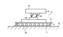
ギャップが設定された2枚の基板1,2は位置合わせ装置11に搬入される。図3に位置合わせ装置11の概略を示す。この位置合わせ装置11は載置テーブル12を有し、この載置テーブル12上にギャップが設定された2枚の基板1,2が供給される。そして、下側に位置する第1の基板1が上記載置テーブル12に、たとえば吸引などの手段によって吸着固定される。
【0018】
載置テーブル12に固定された第1の基板1に対し、第2の基板2を変位させることで、第1の基板1に対して第2の基板2が位置決めされる。第2の基板2を変位させるには、この第2の基板2の上面を位置合わせヘッド13で吸着する。この位置合わせヘッド13は、水平方向に駆動される可動体14の取付け部15に取付けられており、この可動体14とともに移動することで、上記第2の基板2を第1の基板1に対して相対的に変位させる。
【0019】
なお、第1の基板1と第2の基板2との間にはスペーサ材16が設けられている。スペーサ材16としては球状のミクロパールや柱状のスーパスペーサが用いられる。
【0020】
位置合わせ装置11によって2枚の基板1,2を高精度に位置合わせする際、位置合わせする機構にはシール剤3の抵抗がかかることになる。この実施の形態では上記取付け部15に抵抗がかかる。そのため、その抵抗力によって上記取付け部15に撓みが生じ、上記可動体14に与えられた指令量に対し、第2の基板2の実際の変位量が伴わないことになる。
【0021】
これを定量的な式で求めるとつぎのようになる。つまり、位置合わせの指令量X、実際の第2の基板2の移動量η、2枚の基板1,2間の抵抗L、取付け部15を含む可動体14のばね定数(剛性)K1とすると、釣り合いの式から、
K1・(X(t)−η(t))=L(t) …(1)式
が成立する。なお、(t)は時間の関数を意味する。
【0022】
上記(1)式より、実際の第2の基板2の変位量η(t)は、
η(t)=X(t)−(L(t)/K1) …(2)式
ここで、指令量Xに対する第2の基板2の変位量η(t)の不足量をΔとすると、
Δ=X(t)−η(t)=L(t)/K1 …(3)式
となる。よって、指令量X(t)に予め不足量Δを付加した指令量X1は、
X1(t)=Δ+X(t)=L(t)/K1+X(t) …(4)式
となるから、指令量X1(t)を与えてやれば、指令に対する実際の第2の基板2の移動量の不足はなくなる。
【0023】
なお、図4はこの発明の位置合わせ装置1のモデル図である。
【0024】
ここで、基板1,2間の抵抗L(t)はシール剤3の抵抗であり、シール剤3や基板1,2などの材料条件で決まる固有値である。この値は、材料物性もしくは実験で求めることができるし、或いは実際に位置合わせ装置11の駆動モータのトルク値からも換算することができる。
【0025】
上述した指令方法をとることで、今まで不足量を補うかたちで繰り返していた位置合わせを、1回の位置合わせで行うことができる。
【0026】
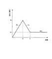
つぎに、基板1,2間の抵抗の主要因であるシール剤3の遅れ変形を考慮した指令方法について説明する。シール剤3は粘弾性体であるため、クリープ変形(遅れ変形)を生じる。図5にAで示すように位置合わせヘッド13に一定時間の移動指令を与えた場合、移動指令中は同図にBで示す基板1,2間の抵抗による影響と、位置合わせ装置11のばね定数(剛性)との関係で、基板2は同図にCで示すように不足量をもちながら変位してゆく。そして、移動指令が完了しても、シール剤3の粘性成分に蓄えられた内部応力の影響で、基板2の変位はさらに継続することになる。
【0027】
これらの現象を定式化するとつぎのようになる。図6に示すように、位置合わせ装置11への一回目と2回目の移動指令完了時間をts、tr、同じく1回目と2回目との移動指令速度をV0、V1、可動体14による基板2に加わる垂直荷重をN、シール剤3の粘性をμ、シール剤3の弾性をKsとする。
【0028】
実際に第2の基板2に1回面の位置合わせの指令を与えているとき、つまり(t≦ts)のとき、基板2の変位η(t)は、
η(t)=X(t)−L(t)/K1 …(5)式
となり、基板2の抵抗L(t)は、
L(t)=μV0(1−e−t/λ) …(6)式
となる。ただし、λ=μ/K、1/K=1/K+1/Ksである。
【0029】
位置合わせの指令が完了した(t>ts)の状態での基板2の変位量η(t)は、
η(t)=X(t)−L(t)/K1 …(7)式
となり、基板2の抵抗L(t)は、
L(t)=μV0(1−e−ts/λ)e−(t−ts)/λ …(8)式
となる。遅れ変形を無くすには、指令が完了した後に残る抵抗L(t)をゼロにする方法をとればよい。たとえば、目標位置に対し、一度、この目標位置を超える1回目の指令量を与え、その後、逆方向に戻すような2回目の指令を与えると、抵抗がゼロになる。一方向に与えた1回目の指令が完了するまでの時間をts、逆方向に与えた2回目の指令が完了するまでの時間をtr、目標変位量をXrとすると、(t≦ts)での基板2の抵抗L(t)は、
L(t)=μV0 (1−e−t/λ) …(9)式
となり、(ts>t≦tr)での基板2の抵抗L(t)は、
L(t)=(L(ts)−μV1)e−(t−ts)/λ+μV1
…(10)式
となり、(t>tr )での基板2の抵抗L(t)は、
L(t)=L(ts)e−(t−ts)/λ …(11)式
となる。ここで、L(tr)=0となるようにXs、つまり時間tsにおける抵抗が0となるXsを求めると、
Xs=Xr/A …(12)式
ただし、
A=1−α・e−αts/λ・(1−e−αts/λ/(1−α・e−αts/λ)
…(13)式
tr=(α+1)・ts …(14)式
となる。したがって、求めたXsに基づいて図6に示す1回目と2回目の移動指令速度V0、V1を与えれば、シール剤3の遅れ変形をなくすことができる。
【0030】
このようにして、第2の基板2の位置合わせが終了したならば、位置合わせ装置11に設けられた図示しない紫外線発生器からの紫外線によって仮止め剤5を照射して硬化させる。それによって、位置決めされた第2の基板2を第1の基板1に対して仮固定することができる。
【0031】
第2の基板2を仮固定したならば、これら基板1,2を図1に示すように加圧加熱装置17へ搬入する。この加圧加熱装置17では第1の基板1と第2の基板2との間に設けられたシール剤3を加熱する。それによって、熱硬化性のシール剤3は硬化するから、第1の基板1と第2の基板2とを本固定することができる。本固定後、第1、第2の基板1,2の仮固定された周辺部を除去することで、これら基板1,2の組立てが終了する。
【0032】
上記実施の形態によれば、基板間の抵抗による移動量の不足分や基板間のシール剤の遅れ変形を考慮した最適な位置合わせを行うことができる。
【0033】
【発明の効果】
以上のようにこの発明によれば、ギャップが管理されている液晶パネルを迅速に提供することができる。
【図面の簡単な説明】
【図1】この発明の一実施の形態を示す組立て装置の概略的説明図。
【図2】第1の基板に仮止め剤を塗布した図。
【図3】位置合わせ装置の概略的説明図。
【図4】シール剤を介して接合された一対の基板を位置合わせするときのモデル図。
【図5】指令量に対する基板の変位とシール剤の抵抗との関係の説明図。
【図6】第2の基板に与える指令量の説明図。
【符号の説明】
1…第1の基板
2…第2の基板
3…シール剤
6…貼り合わせ装置
7…加圧装置
11…位置合わせ装置
13…位置合わせヘッド
14…可動体
15…取付け部
16…加圧加熱装置[0001]
BACKGROUND OF THE INVENTION
The present invention relates to an assembling method and an assembling apparatus for a liquid crystal display device constituted by positioning and bonding two glass substrates with a predetermined gap.
[0002]
[Prior art]
When pasting together two translucent glass substrates constituting a liquid crystal panel incorporated in a liquid crystal display device, first apply a thermosetting sealant such as epoxy resin to one substrate and spray spacers. The other substrate is placed opposite to this substrate and temporarily bonded. Next, after pressurizing the upper substrate to set the gap between the two substrates, the lower substrate is fixed and the upper substrate is displaced in the horizontal direction so that the two substrates are aligned. ing. When the position is correct, the sealant is fully cured.
[0003]
When the upper substrate is displaced in the horizontal direction, the sealant behaves as a viscoelastic material unique to the resin. A certain amount of time (referred to as relaxation time or delay time) is required. In addition, when a frictional force works with the displacement of the upper substrate, an error corresponding to the frictional force occurs.
[0004]
For this reason, the actual displacement amount of the substrate may be smaller than the given displacement amount.
[0005]
[Problems to be solved by the invention]
Conventionally, the alignment between two substrates has not been able to quantitatively grasp the resistance between the substrates represented by the sealant, so the alignment is repeated to compensate for the lack of displacement of the substrate. Then, after the delayed deformation after alignment was settled, a method such as further alignment was taken.
[0006]
However, in such a method, since it takes a long time to complete the alignment of the substrate, it may not only cause a decrease in productivity but also affect the alignment accuracy. .
[0007]
It is an object of the present invention to provide a liquid crystal display device assembling method and an assembling device which can align two substrates with a relatively simple method and with high accuracy.
[0008]
[Means for Solving the Problems]
According to the first aspect of the present invention, two substrates are bonded together with a predetermined gap through a sealant made of a viscoelastic body, and one substrate is fixed and the other substrate is displaced, thereby aligning these substrates. In the assembly method of the liquid crystal display device,
A first correction step of displacing the other substrate at aspeed that eliminates delayed deformation of thesealant to a command amount that causes theresistance of the sealant to become zero overa target position;
A second correction step for returning theother substrate to a target position at aspeed that eliminates the delayed deformation of the sealant when the other substrate is displaced to a command amount at which the resistance of the sealant becomes zero. There is a method for assembling the display device.
[0010]
According to a second aspect of the present invention, there is provided an apparatus for assembling a liquid crystal display device in which two substrates are bonded to each other with a predetermined gap through a sealant made of a viscoelastic body.
A laminating apparatus for laminating two substrates through a sealant;
A pressurizing device that pressurizes two bonded substrates to set a gap between the substrates;
An alignment device that fixes one of the two substrates set to a predetermined gap and aligns the other by displacing the other,
The alignment apparatusdisplaces the sealant after the second substrate is displaced to acommand amount that causesthe resistance of the sealant to become zero at aspeed that eliminatesthe delay deformation of the sealant. The liquid crystal display device assembly apparatus is controlled so as to returnto the target position at aspeed of elimination .
[0011]
DETAILED DESCRIPTION OF THE INVENTION
An embodiment of the present invention will be described below with reference to the drawings.
[0012]
As is well known, a liquid crystal display device is constructed by bonding two glass transparent substrates having wiring formed on the surface thereof with a small gap of about 10 μm through a sealing agent, and injecting liquid crystal between these substrates. Is done. In an active matrix liquid crystal display device employing TFTs (thin film transistors), it is required that two substrates be aligned and pasted with an accuracy of 1 μm or less.
[0013]
FIG. 1 is a block diagram showing a schematic configuration of the assembling apparatus of the present invention. The assembling apparatus carries in the first and
[0014]
The
[0015]
The
[0016]
The two
[0017]
The two
[0018]
The
[0019]
A
[0020]
When aligning the two
[0021]
When this is obtained by a quantitative formula, it is as follows. That is, the positioning command amount X, the actual movement amount η of the
K1 · (X (t) −η (t)) = L (t) (1) is established. (T) means a function of time.
[0022]
From the above equation (1), the actual displacement η (t) of the
η (t) = X (t) − (L (t) / K1 ) (2) Equation where Δ is a shortage of the displacement η (t) of the
Δ = X (t) −η (t) = L (t) / K1 (3) Therefore, the command amount X1 obtained by adding the deficient amount Δ to the command amount X (t) in advance is
X1 (t) = Δ + X (t) = L (t) / K1 + X (t) (4) Since the equation (4) is given, if the command amount X1 (t) is given, the actual second The shortage of the movement amount of the
[0023]
FIG. 4 is a model diagram of the
[0024]
Here, the resistance L (t) between the
[0025]
By using the above-described command method, it is possible to perform the alignment that has been repeated until now to compensate for the shortage in a single alignment.
[0026]
Next, a command method that takes into account the delayed deformation of the
[0027]
These phenomena are formulated as follows. As shown in FIG. 6, the first and second movement command completion times for the
[0028]
When a command for positioning the surface once is actually given to the
η (t) = X (t) −L (t) / K1 (5) where the resistance L (t) of the
L (t) = μV0 (1−e−t / λ ) (6) However, it is λ = μ / K, 1 / K = 1 /
[0029]
Instruction alignment is completed (t> ts) the amount of displacement of the
η (t) = X (t) −L (t) / K1 (7) where the resistance L (t) of the
L (t) = μV 0 ( 1-e -ts / λ) e - a(t-ts) / λ ... (8) formula. In order to eliminate the delayed deformation, a method of zeroing the resistance L (t) remaining after the command is completed may be used. For example, when the first command amount exceeding the target position is once given to the target position, and then the second command for returning in the reverse direction is given, the resistance becomes zero. Assuming that time until completion of the first command given in one direction is ts , time until completion of the second command given in the reverse direction is tr , and target displacement is Xr (t ≦ ts) of the
L (t) = μV 0 (1−e−t / λ ) (9) where the resistance L (t) of the
L (t) = (L (ts ) −μV1 ) e−(t−ts) / λ + μV1
(10) The resistance L (t) of the
L (t) = L (ts ) e−(t−ts) / λ (11) Here, L(t r) = 0 and becomes asX s, that is, when obtaining theX s resistance becomes zero at timet s,
Xs = Xr / A (12) where
A = 1- [alpha] e-[ alpha]ts / [lambda]. (1-e-[ alpha]ts / [lambda] / (1- [alpha] e-[ alpha]ts/ [lambda] ).
(13) Formulatr = (α + 1) · ts (14) Therefore, if the first and second movement command speeds V0 and V1 shown in FIG. 6 are given based on the obtained Xs , the delayed deformation of the
[0030]
In this manner, when the alignment of the
[0031]
If the 2nd board |
[0032]
According to the above-described embodiment, it is possible to perform optimum alignment in consideration of the shortage of the movement amount due to the resistance between the substrates and the delayed deformation of the sealant between the substrates.
[0033]
【Effect of the invention】
As described above, according to the present invention, it is possible to quickly provide a liquid crystal panel in which a gap is managed.
[Brief description of the drawings]
FIG. 1 is a schematic explanatory view of an assembling apparatus showing an embodiment of the present invention.
FIG. 2 is a diagram in which a temporary fixing agent is applied to a first substrate.
FIG. 3 is a schematic explanatory diagram of an alignment apparatus.
FIG. 4 is a model diagram when aligning a pair of substrates bonded via a sealant.
FIG. 5 is an explanatory diagram of the relationship between the displacement of the substrate and the resistance of the sealing agent with respect to the command amount.
FIG. 6 is an explanatory diagram of a command amount given to a second substrate.
[Explanation of symbols]
DESCRIPTION OF
Claims (2)
Translated fromJapanese上記他方の基板を上記シール剤の遅れ変形をなくす速度で目標位置を超えて上記シール剤の抵抗がゼロとなる指令量まで変位させる第1の補正工程と、
上記他方の基板が上記シール剤の抵抗がゼロとなる指令量まで変位したときにこの他方の基板を上記シール剤の遅れ変形をなくす速度で目標位置まで戻す第2の補正工程と
を具備する液晶表示装置の組立て方法。In an assembly method of a liquid crystal display device in which two substrates are bonded together with a predetermined gap through a sealant made of a viscoelastic body, one substrate is fixed and the other substrate is displaced, thereby aligning these substrates. ,
A first correction step of displacing the other substrate at aspeed that eliminates delayed deformation of thesealant to a command amount that causes theresistance of the sealant to become zero overa target position;
A second correction step for returning theother substrate to a target position at aspeed that eliminates the delayed deformation of the sealant when the other substrate is displaced to a command amount at which the resistance of the sealant becomes zero. Assembling method of display device.
2枚の基板をシール剤を介して貼り合わせる貼り合わせ装置と、
貼り合わされた2枚の基板を加圧してこれら基板のギャップを設定する加圧装置と、
所定のギャップに設定された2枚の基板の一方を固定し他方を変位させてこれら基板を位置合わせする位置合わせ装置とを具備し、
上記位置合わせ装置は、上記他方の基板を上記シール剤の遅れ変形をなくす速度で目標位置を超えて上記シール剤の抵抗がゼロとなる指令量まで変位させたのち、上記シール剤の遅れ変形をなくす速度で目標位置に戻すよう駆動制御されることを特徴とする液晶表示装置の組立て装置。In an assembly apparatus for a liquid crystal display device in which two substrates are bonded together with a predetermined gap through a sealant made of a viscoelastic material,
A laminating apparatus for laminating two substrates through a sealant;
A pressurizing device that pressurizes two bonded substrates to set a gap between the substrates;
An alignment device that fixes one of the two substrates set to a predetermined gap and aligns the other by displacing the other,
The alignment apparatusdisplaces the sealant after the second substrate is displaced to acommand amount that causesthe resistance of the sealant to become zero at aspeed that eliminatesthe delay deformation of the sealant. An assembly apparatus for a liquid crystal display device, wherein the drive control is performed so as to returnto the target position at aspeed of elimination .
Priority Applications (4)
| Application Number | Priority Date | Filing Date | Title |
|---|---|---|---|
| JP2001269292AJP4880838B2 (en) | 2001-09-05 | 2001-09-05 | Method and apparatus for assembling liquid crystal display device |
| KR10-2002-0053230AKR100498238B1 (en) | 2001-09-05 | 2002-09-04 | Method and apparatus for manufacturing liquid crystal display device |
| US10/234,162US7385667B2 (en) | 2001-09-05 | 2002-09-05 | Method of manufacturing liquid crystal display apparatus and manufacturing device therefor |
| US11/858,657US8096336B2 (en) | 2001-09-05 | 2007-09-20 | Method of manufacturing liquid crystal display apparatus and manufacturing device therefor |
Applications Claiming Priority (1)
| Application Number | Priority Date | Filing Date | Title |
|---|---|---|---|
| JP2001269292AJP4880838B2 (en) | 2001-09-05 | 2001-09-05 | Method and apparatus for assembling liquid crystal display device |
Publications (2)
| Publication Number | Publication Date |
|---|---|
| JP2003075843A JP2003075843A (en) | 2003-03-12 |
| JP4880838B2true JP4880838B2 (en) | 2012-02-22 |
Family
ID=19095141
Family Applications (1)
| Application Number | Title | Priority Date | Filing Date |
|---|---|---|---|
| JP2001269292AExpired - Fee RelatedJP4880838B2 (en) | 2001-09-05 | 2001-09-05 | Method and apparatus for assembling liquid crystal display device |
Country Status (3)
| Country | Link |
|---|---|
| US (2) | US7385667B2 (en) |
| JP (1) | JP4880838B2 (en) |
| KR (1) | KR100498238B1 (en) |
Families Citing this family (33)
| Publication number | Priority date | Publication date | Assignee | Title |
|---|---|---|---|---|
| US7417782B2 (en)* | 2005-02-23 | 2008-08-26 | Pixtronix, Incorporated | Methods and apparatus for spatial light modulation |
| US9082353B2 (en) | 2010-01-05 | 2015-07-14 | Pixtronix, Inc. | Circuits for controlling display apparatus |
| US9087486B2 (en) | 2005-02-23 | 2015-07-21 | Pixtronix, Inc. | Circuits for controlling display apparatus |
| US7999994B2 (en) | 2005-02-23 | 2011-08-16 | Pixtronix, Inc. | Display apparatus and methods for manufacture thereof |
| US7675665B2 (en) | 2005-02-23 | 2010-03-09 | Pixtronix, Incorporated | Methods and apparatus for actuating displays |
| US8519945B2 (en) | 2006-01-06 | 2013-08-27 | Pixtronix, Inc. | Circuits for controlling display apparatus |
| US9158106B2 (en) | 2005-02-23 | 2015-10-13 | Pixtronix, Inc. | Display methods and apparatus |
| US9261694B2 (en) | 2005-02-23 | 2016-02-16 | Pixtronix, Inc. | Display apparatus and methods for manufacture thereof |
| US7304786B2 (en)* | 2005-02-23 | 2007-12-04 | Pixtronix, Inc. | Methods and apparatus for bi-stable actuation of displays |
| US8159428B2 (en) | 2005-02-23 | 2012-04-17 | Pixtronix, Inc. | Display methods and apparatus |
| US9229222B2 (en)* | 2005-02-23 | 2016-01-05 | Pixtronix, Inc. | Alignment methods in fluid-filled MEMS displays |
| US8482496B2 (en) | 2006-01-06 | 2013-07-09 | Pixtronix, Inc. | Circuits for controlling MEMS display apparatus on a transparent substrate |
| US7746529B2 (en) | 2005-02-23 | 2010-06-29 | Pixtronix, Inc. | MEMS display apparatus |
| US7304785B2 (en)* | 2005-02-23 | 2007-12-04 | Pixtronix, Inc. | Display methods and apparatus |
| US8310442B2 (en) | 2005-02-23 | 2012-11-13 | Pixtronix, Inc. | Circuits for controlling display apparatus |
| US20070205969A1 (en) | 2005-02-23 | 2007-09-06 | Pixtronix, Incorporated | Direct-view MEMS display devices and methods for generating images thereon |
| US8526096B2 (en) | 2006-02-23 | 2013-09-03 | Pixtronix, Inc. | Mechanical light modulators with stressed beams |
| EP2264507A3 (en)* | 2007-01-19 | 2011-07-20 | Pixtronix Inc. | A display apparatus |
| US9176318B2 (en) | 2007-05-18 | 2015-11-03 | Pixtronix, Inc. | Methods for manufacturing fluid-filled MEMS displays |
| US7852546B2 (en) | 2007-10-19 | 2010-12-14 | Pixtronix, Inc. | Spacers for maintaining display apparatus alignment |
| US20090133801A1 (en)* | 2007-11-23 | 2009-05-28 | Seok Hee Shim | Substrate attaching apparatus |
| US8169679B2 (en) | 2008-10-27 | 2012-05-01 | Pixtronix, Inc. | MEMS anchors |
| KR20120132680A (en) | 2010-02-02 | 2012-12-07 | 픽스트로닉스 인코포레이티드 | Methods for manufacturing cold seal fluid-filled display apparatus |
| CN102514385B (en)* | 2011-11-29 | 2015-04-15 | 深圳市华星光电技术有限公司 | Identification code printing method and identification code printing device |
| US8823998B2 (en) | 2011-11-29 | 2014-09-02 | Shenzhen China Star Optoelectronics Technology Co., Ltd. | Identification code printing method and printing apparatus |
| US8821659B2 (en)* | 2012-05-14 | 2014-09-02 | Asm Technology Singapore Pte Ltd | Apparatus and method for real-time alignment and lamination of substrates |
| US20140017458A1 (en)* | 2012-07-10 | 2014-01-16 | Nike, Inc. | Temporarily Positionable Meltable Adhesives For Shoe And Apparel Assembly |
| US9134552B2 (en) | 2013-03-13 | 2015-09-15 | Pixtronix, Inc. | Display apparatus with narrow gap electrostatic actuators |
| CN103487996A (en)* | 2013-09-24 | 2014-01-01 | 深圳市华星光电技术有限公司 | Method for alignment and combination of array substrate and color film substrate of liquid crystal display |
| CN104793376A (en)* | 2015-05-19 | 2015-07-22 | 合肥京东方光电科技有限公司 | Liquid crystal display panel poor alignment repairing equipment |
| CN107305818A (en)* | 2016-04-18 | 2017-10-31 | 致伸科技股份有限公司 | Assembling method of backlight module and assembling system applying same |
| CN107359285B (en)* | 2017-08-18 | 2019-03-15 | 武汉华星光电半导体显示技术有限公司 | A kind of OLED display and preparation method thereof |
| CN109143651A (en)* | 2018-09-30 | 2019-01-04 | 京东方科技集团股份有限公司 | The preparation method of substrate for display motherboard, display panel motherboard and display panel |
Family Cites Families (15)
| Publication number | Priority date | Publication date | Assignee | Title |
|---|---|---|---|---|
| US5078477A (en)* | 1988-11-09 | 1992-01-07 | Mitsubishi Gas Chemical Company, Inc. | Ferroelectric liquid crystal cell |
| JPH04271320A (en)* | 1991-02-27 | 1992-09-28 | Ii & S:Kk | Apparatus for producing liquid crystal display |
| JPH05232451A (en)* | 1992-02-21 | 1993-09-10 | Toshiba Corp | Substrate alignment method and apparatus |
| JPH0634983A (en)* | 1992-07-17 | 1994-02-10 | Sharp Corp | Sticking device |
| US5898041A (en)* | 1995-03-01 | 1999-04-27 | Matsushita Electric Industrial Co., Ltd. | Production process of liquid crystal display panel, seal material for liquid crystal cell and liquid crystal display |
| JPH09197361A (en)* | 1996-01-12 | 1997-07-31 | Toshiba Corp | Substrate alignment device and substrate alignment method |
| JP4038272B2 (en)* | 1997-06-04 | 2008-01-23 | 東芝松下ディスプレイテクノロジー株式会社 | Method and apparatus for assembling liquid crystal display device |
| JP3536651B2 (en)* | 1998-03-18 | 2004-06-14 | セイコーエプソン株式会社 | Substrate bonding apparatus, substrate bonding method, and liquid crystal device manufacturing method |
| US6193576B1 (en)* | 1998-05-19 | 2001-02-27 | International Business Machines Corporation | TFT panel alignment and attachment method and apparatus |
| JP3828670B2 (en)* | 1998-11-16 | 2006-10-04 | 松下電器産業株式会社 | Manufacturing method of liquid crystal display element |
| US6104466A (en)* | 1999-01-07 | 2000-08-15 | International Business Machines Corporation | Precision alignment of plates |
| JP3441412B2 (en)* | 1999-10-29 | 2003-09-02 | シャープ株式会社 | Resin-sealed semiconductor device and liquid crystal display module using the same |
| JP2001264780A (en) | 2000-03-17 | 2001-09-26 | Toshiba Corp | Manufacturing apparatus and manufacturing method for liquid crystal display device |
| JP3492284B2 (en)* | 2000-04-19 | 2004-02-03 | 株式会社 日立インダストリイズ | Substrate bonding device |
| KR100757488B1 (en)* | 2001-05-22 | 2007-09-11 | 엘지.필립스 엘시디 주식회사 | Substrate Size Control Method of LCD |
- 2001
- 2001-09-05JPJP2001269292Apatent/JP4880838B2/ennot_activeExpired - Fee Related
- 2002
- 2002-09-04KRKR10-2002-0053230Apatent/KR100498238B1/ennot_activeExpired - Fee Related
- 2002-09-05USUS10/234,162patent/US7385667B2/ennot_activeExpired - Fee Related
- 2007
- 2007-09-20USUS11/858,657patent/US8096336B2/ennot_activeExpired - Fee Related
Also Published As
| Publication number | Publication date |
|---|---|
| KR20030023491A (en) | 2003-03-19 |
| US20080011418A1 (en) | 2008-01-17 |
| US20030043337A1 (en) | 2003-03-06 |
| KR100498238B1 (en) | 2005-07-01 |
| US7385667B2 (en) | 2008-06-10 |
| US8096336B2 (en) | 2012-01-17 |
| JP2003075843A (en) | 2003-03-12 |
Similar Documents
| Publication | Publication Date | Title |
|---|---|---|
| JP4880838B2 (en) | Method and apparatus for assembling liquid crystal display device | |
| CN106910429B (en) | A kind of flexible die group and preparation method thereof | |
| JP3220403B2 (en) | Display device manufacturing method | |
| CN102169250B (en) | Manufacturing method of flat-panel display device and bonding press apparatus therefor | |
| US5528403A (en) | Flat type display device having flexible wiring board and common wiring board bonded to display panel | |
| CN101515079A (en) | Manufaturing method of display device | |
| JP2009048214A (en) | Display device manufacturing method and bonding method | |
| TW200624967A (en) | Apparatus for applying a photo curing resin and method of applying a photosetting | |
| CN106154608A (en) | Conducting resinl adhering device and the preparation method of display floater | |
| CN104411789A (en) | Member laminating device | |
| CN211236503U (en) | A device for assembling a backplane and a frame of a liquid crystal display | |
| TWI335458B (en) | Liquid crystal panel module and method for manufacturing a liquid crystal display panel thereof | |
| JPH1114827A (en) | Polarizing plate sticking device | |
| JP5624594B2 (en) | Display device manufacturing apparatus and display device manufacturing method | |
| JPH07181455A (en) | Display device | |
| JPH05109482A (en) | Method for manufacturing thin film EL panel with sealing plate and thin film EL panel with sealing plate | |
| JP3751908B2 (en) | Pressure sealing device and liquid crystal panel manufacturing method | |
| JP2929754B2 (en) | Manufacturing method of liquid crystal display device | |
| JP2003280543A (en) | Display device and method of manufacturing the same | |
| JPS58173715A (en) | Production of liquid crystal display panel | |
| JP2011218474A (en) | Method and apparatus for separating multilayered plate member having adhesive layer | |
| JP2626231B2 (en) | Bonding method of slider and suspension of magnetic head | |
| JPH04195121A (en) | Production of liquid crystal display element | |
| KR19990034424A (en) | Pressing device for bonding integrated circuit elements | |
| JPH0359530A (en) | Manufacture of liquid crystal display panel |
Legal Events
| Date | Code | Title | Description |
|---|---|---|---|
| A621 | Written request for application examination | Free format text:JAPANESE INTERMEDIATE CODE: A621 Effective date:20080728 | |
| A977 | Report on retrieval | Free format text:JAPANESE INTERMEDIATE CODE: A971007 Effective date:20110322 | |
| A131 | Notification of reasons for refusal | Free format text:JAPANESE INTERMEDIATE CODE: A131 Effective date:20110329 | |
| A521 | Written amendment | Free format text:JAPANESE INTERMEDIATE CODE: A523 Effective date:20110530 | |
| TRDD | Decision of grant or rejection written | ||
| A01 | Written decision to grant a patent or to grant a registration (utility model) | Free format text:JAPANESE INTERMEDIATE CODE: A01 Effective date:20111108 | |
| A01 | Written decision to grant a patent or to grant a registration (utility model) | Free format text:JAPANESE INTERMEDIATE CODE: A01 | |
| A61 | First payment of annual fees (during grant procedure) | Free format text:JAPANESE INTERMEDIATE CODE: A61 Effective date:20111202 | |
| FPAY | Renewal fee payment (event date is renewal date of database) | Free format text:PAYMENT UNTIL: 20141209 Year of fee payment:3 | |
| LAPS | Cancellation because of no payment of annual fees |