JP4880122B2 - System for measuring the polarimeter spectrum and other properties of a sample - Google Patents
System for measuring the polarimeter spectrum and other properties of a sampleDownload PDFInfo
- Publication number
- JP4880122B2 JP4880122B2JP2000598823AJP2000598823AJP4880122B2JP 4880122 B2JP4880122 B2JP 4880122B2JP 2000598823 AJP2000598823 AJP 2000598823AJP 2000598823 AJP2000598823 AJP 2000598823AJP 4880122 B2JP4880122 B2JP 4880122B2
- Authority
- JP
- Japan
- Prior art keywords
- sample
- radiation
- focusing
- collecting
- analyzing
- Prior art date
- Legal status (The legal status is an assumption and is not a legal conclusion. Google has not performed a legal analysis and makes no representation as to the accuracy of the status listed.)
- Expired - Fee Related
Links
- 238000001228spectrumMethods0.000titleclaimsdescription53
- 230000005855radiationEffects0.000claimsdescription102
- 238000000034methodMethods0.000claimsdescription61
- 230000010287polarizationEffects0.000claimsdescription43
- 230000003287optical effectEffects0.000claimsdescription24
- 238000004458analytical methodMethods0.000claimsdescription12
- 230000033001locomotionEffects0.000claimsdescription5
- 239000011248coating agentSubstances0.000claimsdescription4
- 238000000576coating methodMethods0.000claimsdescription4
- 239000006185dispersionSubstances0.000claimsdescription4
- 230000003111delayed effectEffects0.000claims1
- 230000009466transformationEffects0.000claims1
- 238000005286illuminationMethods0.000description36
- 238000005259measurementMethods0.000description25
- 239000002131composite materialSubstances0.000description22
- 238000000985reflectance spectrumMethods0.000description10
- 238000005452bendingMethods0.000description8
- 238000010586diagramMethods0.000description8
- 239000010408filmSubstances0.000description8
- 230000003595spectral effectEffects0.000description8
- 239000010409thin filmSubstances0.000description6
- 238000001514detection methodMethods0.000description5
- 230000005684electric fieldEffects0.000description4
- 238000012986modificationMethods0.000description4
- 230000004048modificationEffects0.000description4
- 238000000391spectroscopic ellipsometryMethods0.000description4
- 229910052724xenonInorganic materials0.000description4
- FHNFHKCVQCLJFQ-UHFFFAOYSA-Nxenon atomChemical compound[Xe]FHNFHKCVQCLJFQ-UHFFFAOYSA-N0.000description4
- YZCKVEUIGOORGS-OUBTZVSYSA-NDeuteriumChemical compound[2H]YZCKVEUIGOORGS-OUBTZVSYSA-N0.000description3
- 230000000903blocking effectEffects0.000description3
- 230000001066destructive effectEffects0.000description3
- 229910052805deuteriumInorganic materials0.000description3
- 238000000572ellipsometryMethods0.000description3
- 238000001914filtrationMethods0.000description3
- 238000007689inspectionMethods0.000description3
- 230000035945sensitivityEffects0.000description3
- VYPSYNLAJGMNEJ-UHFFFAOYSA-NSilicium dioxideChemical compoundO=[Si]=OVYPSYNLAJGMNEJ-UHFFFAOYSA-N0.000description2
- 230000000694effectsEffects0.000description2
- 230000010363phase shiftEffects0.000description2
- 230000002159abnormal effectEffects0.000description1
- 238000003491arrayMethods0.000description1
- 238000000701chemical imagingMethods0.000description1
- 230000000295complement effectEffects0.000description1
- 230000002596correlated effectEffects0.000description1
- 230000000875corresponding effectEffects0.000description1
- 239000013078crystalSubstances0.000description1
- 230000007423decreaseEffects0.000description1
- 230000001419dependent effectEffects0.000description1
- 239000000835fiberSubstances0.000description1
- 239000005350fused silica glassSubstances0.000description1
- 238000007654immersionMethods0.000description1
- 239000000463materialSubstances0.000description1
- 230000007935neutral effectEffects0.000description1
- 230000001902propagating effectEffects0.000description1
- 239000004576sandSubstances0.000description1
- 239000004065semiconductorSubstances0.000description1
- WFKWXMTUELFFGS-UHFFFAOYSA-NtungstenChemical compound[W]WFKWXMTUELFFGS-UHFFFAOYSA-N0.000description1
- 229910052721tungstenInorganic materials0.000description1
- 239000010937tungstenSubstances0.000description1
Images


Classifications
- G—PHYSICS
- G01—MEASURING; TESTING
- G01J—MEASUREMENT OF INTENSITY, VELOCITY, SPECTRAL CONTENT, POLARISATION, PHASE OR PULSE CHARACTERISTICS OF INFRARED, VISIBLE OR ULTRAVIOLET LIGHT; COLORIMETRY; RADIATION PYROMETRY
- G01J4/00—Measuring polarisation of light
- G01J4/02—Polarimeters of separated-field type; Polarimeters of half-shadow type
- G—PHYSICS
- G01—MEASURING; TESTING
- G01J—MEASUREMENT OF INTENSITY, VELOCITY, SPECTRAL CONTENT, POLARISATION, PHASE OR PULSE CHARACTERISTICS OF INFRARED, VISIBLE OR ULTRAVIOLET LIGHT; COLORIMETRY; RADIATION PYROMETRY
- G01J3/00—Spectrometry; Spectrophotometry; Monochromators; Measuring colours
- G01J3/28—Investigating the spectrum
- G01J3/447—Polarisation spectrometry
- G—PHYSICS
- G01—MEASURING; TESTING
- G01N—INVESTIGATING OR ANALYSING MATERIALS BY DETERMINING THEIR CHEMICAL OR PHYSICAL PROPERTIES
- G01N21/00—Investigating or analysing materials by the use of optical means, i.e. using sub-millimetre waves, infrared, visible or ultraviolet light
- G01N21/17—Systems in which incident light is modified in accordance with the properties of the material investigated
- G01N21/21—Polarisation-affecting properties
Landscapes
- Physics & Mathematics (AREA)
- Spectroscopy & Molecular Physics (AREA)
- General Physics & Mathematics (AREA)
- Analytical Chemistry (AREA)
- Life Sciences & Earth Sciences (AREA)
- Chemical & Material Sciences (AREA)
- Health & Medical Sciences (AREA)
- Biochemistry (AREA)
- General Health & Medical Sciences (AREA)
- Immunology (AREA)
- Pathology (AREA)
- Investigating Or Analysing Materials By Optical Means (AREA)
- Length Measuring Devices By Optical Means (AREA)
Description
Translated fromJapanese【0001】
【発明の属する技術分野】
この発明は一般には、試料の表面特性を測定する非破壊技術に関し、特に試料の偏光計スペクトルおよび他の特性を測定するシステムに関する。
【0002】
【従来の技術】
多くの工業的利用にとって、薄膜の厚さやその屈折率のような試料の表面パラメータを測定することは有用である。これらのパラメータは、多くの技術によって測定され得る。よく知られた非破壊検査技術の中に、分光反射解析法と分光学的偏光解析法がある。
【0003】
分光反射解析法において、入射放射ビームは試料で反射し、そして反射放射線の強度が分析されて試料の特性を測定する。入射放射線は多重波長成分を含んでいるから、測定データのスペクトル(反射率スペクトルまたは相対反射率スペクトルとして知られている)が計測される。米国特許第5,747,813号が一種の広帯域分光反射計を記述しており、この特許は引用により完全な形で本明細書に含まれる。
【0004】
分光学的偏光解析装置が米国特許第5,608,526号に記載されており、これは引用により完全な形で本明細書に含まれる。この特許に記載されているように、既知の偏光状態を有する入射放射ビームが試料から概して大きな入射角度で反射され、反射放射線の偏光が分析されて試料の特性を測定する。反射放射線の偏光は入射ビームのそれとは変わるから、量的なおよび相的な偏光状態の変化が測定されて、試料表面の薄膜の厚さと屈折率が測定される。
【0005】
分光反射解析法は、分光学的偏光解析法よりはシンプルで廉価であるが、分光学的偏光解析法は、分光反射解析法よりはより精確で、表面特性に対して感応度が高い。分光反射解析法と分光学的偏光解析法は有用な非破壊検査技術であるが、表面の複屈折のようなある種の表面パラメータを測定することが困難である。
【0006】
従って、複屈折のような表面パラメータを測定するための改良された測定システムを提供することが望ましい。また、上述の非破壊検査技術を補足するために試料表面の特性を測定する偏光計システムを提供することも望ましい。
【0007】
【課題を解決するための手段】
本出願人によって提案された偏光計システムは、分光反射計の単純性を維持するが、分光学的偏光解析装置と同様な表面特性に対する感応度を持っている。広帯域放射線の偏光サンプルビームは、試料表面に集束され、試料によって修正された放射線が集められる。試料に集束されたサンプルビームは、多数の偏光状態を有している。試料によって修正された放射線は、偏光面に関して分析されて偏光計スペクトルを生ずる。そして、厚さと屈折率の情報は、スペクトルから求められる。好ましくは、サンプルビームの偏光は、集束と試料とによってのみ変えられ、分析は、固定偏光面に関して行われる。
【0008】
好適な実施例において、サンプルビームの集束と修正された放射線の収集は、試料内の複屈折軸の存否を検出するために2個の異なる開口を使用して繰り返される。他の実施例において、上述の技術は、薄膜の厚さと屈折率とを測定するために、偏光解析法と組み合わされる。
【0009】
【発明の実施の形態】
図示における簡明さのために、同一部材は同じ符号で示されている。
図1は、本発明の好適な実施例を例示するための、分光学的偏光解析装置と偏光計システムとを有する複合装置の概要図である。複合装置の分光学的偏光解析装置を説明する前に、先ず偏光計システム8が図1および図2を参照してある程度詳しく説明される。以下に示すように、好ましくはシステム8は、図1の複合装置の分光学的(または単一波長の)偏光解析装置と一緒に使用されると有利であるが、このシステムはまた試料を測定するためにそれ自身で効果的に使用することもできる。
【0010】
偏光計システム8の全体的な光学的配置は、米国特許第5,747,813号に記載された分光反射計に類似しており、そのシンプルさを維持している。しかしながら、かかる分光反射計とは異なり、本発明のシステム8は、米国特許第5,747,813号のシステムにおける偏光無感応の反射率スペクトルではなく偏光計反射率スペクトルを測定する。従って、システム8は、米国特許第5,747,813号のシステムよりは表面特性に対して感応度が高い。好適な実施例において、本発明は試料によって反射される放射線を検出するものとして例示されているが、本発明は、試料によって伝播される放射線が代わって検出されると本明細書に記載されているように本質的に作用し、このようなまたは他の変形は本発明の範囲内にある。平易にするために、好適な実施例は、以下に反射放射線を測定するものとして説明されるが、かかる説明は伝播放射線を測定するために容易に拡張されることができると理解される。
【0011】
サンプル経路、参照経路、領域照明経路、測定照明経路、および偏光解析装置経路を示すための凡例が図1の右上隅に示されている。上述したように、偏光計パラメータを測定するシステムの全体的な光学的配置が図1および図2を参照して以下に説明される。
【0012】
図1および図2の各々は、偏光計パラメータを測定するための本発明による光学システムの同じ実施例を示している。システム8の集束部材と他の光学部材および図1の分光学的偏光解析装置は部分的に図2では省略されていて、図面を簡潔にしている。その部材は、他の部材に関するその位置を最も明瞭に示す図面と関連して以下に説明される。図1を参照するに、ウェハ3の相対反射率スペクトルを測定する光学システム8は、照明サブシステム、反射計サブシステム、観察サブシステム、および自動焦点サブシステムを有し、任意の光学部材は複数のサブシステムの一部となることがある。照明サブシステムは、キセノンアークランプのような、可視光および/または紫外(UV)光の光ビーム12を放出するランプ10、ランプハウジング窓14、偏芯放物面鏡16、出し入れ式紫外線遮断フィルタ18、カラーフィルタリング20、平面鏡22、凹面鏡24、出し入れ式40μm微細焦点開口30を備えた開口ミラー28、大アクロマート32,領域照明シャッター31,屈曲ミラー36および小アクロマート38を有する。図2において、対物レンズ40は、ミラーとミラー40a,40bを取り囲むハウジング40’を有するが、分光学的偏光解析装置(図2には図示せず)からの傾斜照明ビームのためにハウジングとウェハとの間に十分な空間を残している。
【0013】
照明システムは、測定ビーム25と領域照明ビーム34とからなる複合ビーム42を供給する。ランプ10は、ランプハウジング窓14を通して光ビーム12を放出する。ランプハウジング窓は光学的理由では必要がないが、ランプが亀裂を生じて破裂したときにランプ10を閉じこめるために設けられる。キセノンランプは、UVから近赤外までのスペクトルをカバーする平坦な出力を生ずるので、タングステンランプや重水素ランプ等の他のランプより好ましい。190〜220nmを含む領域の波長成分を有するサンプルビームを供給するために、キセノンランプ10と組み合わせて重水素ランプ88が追加的に使用され、深紫外を含むより広いスペクトルをカバーする。2個のランプを一緒に使用することによって、試料を検出するために供給される放射線の合成複合スペクトルは、約190nm乃至800または830nmまで拡張されることができる。スペクトルを深紫外領域まで拡大することは、写真印刷にとって有用である。ランプ88からの放射線は、レンズ93によって集束され、ミラー95によってフィルタ18に向けて反射され、そしてランプ10からの放射線と組み合わされて複合ビーム12’を形成する。矢印99に沿うビーム12の経路の内外にミラー95を動かすことによって、重水素ランプ88からの放射線を測定ビーム25に含ませたり除外したりすることが可能である。
【0014】
偏芯放物面鏡16は、光ビーム12を平行にし、これはランプ88からの放射線と組み合わされてビーム12’を形成した後、出し入れ式紫外線遮断フィルタ18とカラーフィルタリング20とによって選択的に濾波される。出し入れ式紫外線遮断フィルタ18は、光ビーム12’のスペクトルを制限するために部分的に使用されるから、光ビーム12’が回折格子によって分光されるときに、1次および2次分光は重なり合わない。ビーム12’は平面鏡22によって凹面鏡24上に部分的に反射されて測定ビーム25を形成する。凹面鏡24は測定ビーム25を開口ミラー28の開口上に集束する。
【0015】
光ビーム12の他の部分、すなわち領域照明ビーム34は、大アクロマート32によって屈曲ミラー36の近くに集束され、屈曲ミラー36をしてランプ10、88の像を小アクロマート38に向けて反射させる。小アクロマート38は、光が開口ミラー28で反射する前に領域照明ビーム34内の光を集める。開口ミラー28は、一面に反射コーティングがなされた溶融シリカ板であり、反射コーティングからエッチングされた150μm2 が測定ビーム25用の開口を生ずる。開口は、対物レンズ40の共役軸にある。領域照明は、領域照明ビーム34の光路内に領域照明シャッター31を置くことにより遮断される。
【0016】
狭い測定ビーム25と広幅の領域照明ビーム34は、開口ミラー28で再合体し、領域照明ビーム34は開口ミラー28の前で反射し、測定ビーム25は開口と偏光子102を通過し、これはモータ101によってビーム25の経路に出入りされる。
【0017】
図1は反射計と、光学システム8の観察サブシステムおよび自動焦点サブシステムとを示しているが、対物レンズ40、ビーム分割ミラー45,サンプルビーム46,オプションの参照ビーム48,凹面鏡50,平面鏡43,参照分光ピンホール56を備えた参照板52,サンプル分光ピンホール58を備えたサンプル板54、第2の屈曲ミラー68,回折格子70,サンプル線状フォトダイオードアレー72,参照線状フォトダイオードアレー74,短焦点距離を有するアクロマート80,ミラー82,ビーム分割キューブ84,五角プリズム86,長焦点距離を有するアクロマート90,中立密度フィルタリング97,第3の屈曲ミラー91,およびビデオカメラ96を有している。これらの構成要素のいくつかは、明確化のために図2には示されていない。
【0018】
対物レンズ40にとって、いくつかの拡大率は可能である。実施例において、シュバルツチルト(Schwarzchild)設計の全反射対物レンズは、回転ターレットに載せられ、これはいくつかの異なる対物レンズ(図示せず)の一つをサンプルビーム46の光路内に置くことを可能とする。本発明における測定に著しい影響を与えずに、サンプルビーム46の光路内に低出力の屈折部材を置くことが可能である。
【0019】
ウェハ3の相対反射率スペクトルの測定が次に説明される。領域照明シャッター31が領域照明ビーム34の経路内に置かれると、複合ビーム42は測定ビーム25のみから構成される。複合ビーム42は、複合ビーム42の半分を対物レンズ40に向かって偏向するように置かれた全反射ミラーであるビーム分割ミラー45によって分けられ、このようにしてサンプルビーム46を形成し、複合ビーム42の偏向されなかった半分は参照ビーム48を形成する。サンプルビーム46とオプションの参照ビーム48は、同じ光源であるランプ10、88から出ているので、そして複合ビーム42は放射状に一様なので、参照ビーム48とサンプルビーム46は、比例的に従属のスペクトル強度を有している。さらに、ビーム分割ミラー45は、全光路内にある部分反射ミラーではなく、光路の半分内にある全反射ミラーであるので、連続広帯域スペクトルが良好な輝度で反射される。
【0020】
参照ビーム48は、当初はビーム分割ミラー45に作用しないが、代わりに凹面鏡50を照射する。凹面鏡50は、少し軸がオフセットしており、このため参照ビーム48はビーム分割ミラー45の背面上に反射し、ここで平面鏡43が参照分光ピンホール56に整列するように参照ビーム48を再反射する。平面鏡43は、参照ビーム48をサンプルビーム46に再整合するように設けられているため、両ビームはそれらのそれぞれの分光ピンホールを実質的に平行に通過する。参照ビームはサンプルビームと平行に分光計に入るので、このことは両チャンネルに対する分光計部材の簡単な整合を可能とする。
【0021】
参照ビーム48は、ビーム46を反射するビーム分割ミラー45の表面に作用しないので、参照ビーム48がビーム分割ミラー45を通過するときに参照強度の損失が無い。参照ビーム48は、ビーム分割ミラー45の背面のミラー43に作用するが、光がビーム分割ミラー45を通過しないので、これらの2個のミラーは独立している。事実、ビーム分割ミラー45の2個の反射面が容易には1つの光学素子に一緒に置かれない別の実施例においては、複数の反射面は複数の分離ミラー部材上に存在する。
【0022】
凹面鏡50の焦点距離は、参照ビーム48が参照分光計ピンホール56に焦点を結ぶようになっている。参照分光計ピンホール56を通過し屈曲ミラー68で反射する光は、回折格子70により分散される。生成された1次分散光は参照線状フォトダイオードアレー74によって集められ、これにより相対参照スペクトルを測定する。
【0023】
偏光サンプルビーム46は、ビーム分割ミラー45から対物レンズ40に向けて反射され、ここでサンプルビーム46はウェハ3の上に集束され、そして反射サンプルビーム46’が対物レンズ40によってサンプル分光計ピンホール58上に集束される。反射サンプルビーム46’は、ビーム分割ミラー45の背後の参照ビーム48も通過する空間を通過するので、反射サンプルビーム46’は反射経路上でビーム分割ミラー45に作用しない。試料3からの反射サンプルビーム46’の放射線は、ピンホール58に達する前に分析器104を通過する。サンプル分光計ピンホール58を通過し屈曲ミラー68で反射する光は、光の波長に応じて回折格子70により分散される。参照ビームと共に、サンプルビームの生成1次分散ビームはサンプル線状フォトダイオードアレー72によって集められ、これによりサンプル偏光計スペクトルを計測する。2本のビームが回折格子70で交差するので、図2においてサンプルビーム46に明らかに整列したフォトダイオードアレーは、実際参照ビーム48用フォトダイオードアレーであり、また逆である。偏光子102と分析器104は回転せず、好ましくは静止している。従って、分析器104は、試料によって修正され、かつ対物レンズ40によって集められた放射線を固定偏光面に従って分析する。
【0024】
それから、相対反射率スペクトルは、各波長におけるサンプル光強度を各波長における相対参照強度によって割ることにより簡単に得られる。典型的には、これは、512個のダイオードの線状フォトダイオードアレーがサンプルスペクトルおよび参照スペクトルを記録するために使用される512回の割り算計算を含んでいる。好適な実施例において、スペクトルは約190nmから800または830nmまでの範囲に亘っている。
【0025】
本発明の実施例において、回折格子70は凹面のホログラフィック格子であり、分光計ピンホールは15mm離れている。その15mmの間隔は、両ビームが格子上に中心合わせすることを許さないので、回折格子はホログラフィック技術によりマルチスペクトルを結像するように訂正される。このような格子は、インスツルメンツSAによって供給されるマルチスペクトル結像格子である。また、格子は、検出器の角度が検出器からの反射を格子から外れるように設計されている。
【0026】
領域照明を含んでいるかもしれない複合ビーム42は、ビーム分割ミラー45からウェハ3に向かって反射される。反射率スペクトル測定と自動焦点が行われているとき、領域照明は分散光を最小化するように切られる。
【0027】
相対反射率スペクトルを測定するために使用される光学要素の革新的な配置のために、スペクトル測定サブシステムの多くの要素がまた自動焦点サブシステムにも使用される。例えば、図示された実施例の相対反射率スペクトル測定が、部分反射ミラーに対向するビーム分割ミラー45を使用しているので、ウェハ3から反射される生成ビームは、非対称円形断面を有している。このため、焦点整合状態を達成するために対物レンズ40またはウェハ3を動かす相対距離のみならず焦点方向を検出することを可能とするが、対称円形断面を用いては焦点方向を検出することはできない。
【0028】
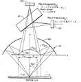
図1および図2の偏光計システム8は、サンプルビーム46が本出願のシステムにおいて偏光している点で米国特許第5,747,813号に記載されたものとは異なっている。このように、サンプルビーム46が対物レンズ40によって試料3に向かって反射されると、ウェハ上に焦点を結ぶビームは多数のまたは複数の異なる偏光状態を持つ。これが図3Aおよび図3Bに関連してより明瞭に説明される。サンプルビーム46はミラー40aによってミラー40bに向かって反射され、それからこれは図3Aに示されるようにビームを試料3に向けて集束する。図3Bは、ウェハ3に焦点整合したときのサンプルビーム46の照明開口を示す概念図である。図3A、図3Bにおける種々の量は、円柱座標ρ、φ、θを基準として定義され、ここでρは座標系における点の腕長(原点からの距離)、φは試料表面に対して垂直である参照面に対する該点を含み該試料面に対して垂直な面の角度であり、そして、θは、試料表面の法線からの該点を原点に結ぶ線の角度(法線に対する入射角)である。
【0029】
図3Aを参照するに、偏光子102は角度φP における面によって定義される偏光面を有しているから、その偏光子から出てビーム分割器45によって反射されるサンプルビーム46はまたこの偏光を持っていると仮定される。ビーム46は、先ずミラー40aによって反射され、ビームを試料3上に集束するミラー40bによってその後に反射されると、試料3に集束したビームは図3A、図3Bに示されるように、異なる入射面に入る。図3Bにおいて、ビーム46の偏光面φP は103で示されている。
【0030】
以上の説明から、ビーム分割ミラー45は偏光ビームの約半分を偏向してサンプルビーム46とし、ビームの残り半分を参照ビーム48として通過させる。このような理由で、図3Bの照明開口(陰付き領域106)はほとんど半円形状となる。このようにして対物レンズ40によって試料3上に集束される放射線は、半円形領域を跨ぐ入射面で試料に入射する。領域内の角度φの1値の入射面内でウェハに入射する放射線は、領域内の角度φの異値を有する入射面における放射線のそれとは異なるs分極およびp分極を有する。異なる入射面内の放射線のs分極およびp分極は、定義により、異なる向きを持つので、その一入射面内の入射放射線の偏光状態は、異なる入射面における入射放射線のそれとは異なるものとなる。従って、試料3上に入射する放射線は、φの関数としての多くのすなわち複数の偏光状態を持つことになる。
【0031】
試料3上に集束されるビームは、以下に説明されるように対物レンズ40a,40bの合成反射係数の関数としてサンプルビーム46と対比されて強度が減少する。サンプルビーム46から生じて対物レンズ40により試料上に集束された放射線は、試料により反射され、これは再び強度を減じ、試料の反射係数の関数として各偏光成分の相を変える。このような放射線は再び対物レンズ40によってビーム分割器45と分析器104とを通って上述した分光器に反射される。好適な実施例において、放射線を試料に集束するために使用された同じ対物レンズがまた、分析器と分光器に向かう反射放射線を収集するために使用されるけれども、これは必要なことではなく、異なる収集対物レンズが集束対物レンズに加えて使用できること、そしてその様なまたは別の改変も本発明の範囲に入ることが理解される。
【0032】
試料表面上の原点に向かうφP 方向の分極を有する半円形照明開口内にある図3Aの座標(ρ、φ)を持つ点105からの入射放射線を考えてみる。電界は、以下のように図3A、図3Bに示されるs分極とp分極に分解される。
検出器電流は以下のように表される。
【0034】
幾つかの特殊ケースが以下に示される。
A.φ0 =π
以上の分析から、式(4)および(6)の第3項のcos(Δo +Δs )係数は、偏光子と分析器の角度が同じときに、すなわち、偏光子102と分析器104とが実質的に同じ偏光面を持つときに最大になる。換言すれば、図4に示されるように、偏光子および分析器の両方として機能する単一の偏光子を使用できる。図4に示されるように、偏光子116が、偏光子102と分析器104とを置換するように使用できる。フォトダイオードアレーのサンプルチャネルは、式(5)に比例する。この構成において、一つの偏光子のみが必要であり、偏光子と分析器は自己整合である。さらに別の代替例として、もし分割器45が偏光ビームスプリッタであれば、偏光子102と分析器104が一緒に省略される。膜厚検出の感度を改良するために、図1において、点線で示される波板または遅延素子190がビーム分割器45と分析器104の間に挿入されて、式(4)および(6)の第3項の余弦係数cos(Δo +Δs )の議論に移相を導入する。好ましくは、分析および分散の前に素子190によって生ずる収集放射線の移相は、約π/4である。ミラー40a、40bのミラーコーティングの厚さがまた、薄膜の厚さの検出の感度を増大するために選択されるから、ミラー40a、40bに焦点整合し集められる放射線の相の全変化は、約π/2である。そしてこれは、式(4)および(6)の第3項の余弦係数cos(Δo +Δs )の議論において、Δo をπ/2とするので、これらの式の余弦項は、正弦項に変換される。
【0036】
アレー72の検出器電流に関して測定された偏光計スペクトルは、試料3についての有用な情報を得るのに使用される。例えば、もし試料3の多くの異層の物質の型がその屈折率を推算できるように知られていれば、かかる検出器電流は、層の厚さと精確な屈折率を得るのに十分である。その様な推論の方法は当業者には知られており、ここで詳細に述べる必要は無い。代替的に、検出器信号は、膜厚と屈折率を得るために、偏光解析装置の測定結果と組み合わされる。多くの異なる波長におけるデータポイントを得ることができるので、偏光計システムにおいて検出用に広帯域放射線を使用することは有利である。このような豊富なデータポイントは、試料上の多層の厚さおよび屈折率を測定するために非常に有用であり、そしてより精確な曲線適合アルゴリズムを適用し、または測定値の精度をクロスチェックすることを可能とする。
【0037】
システム8はまた、2回の測定により面内複屈折試料を分析するために使用できるが、その測定の各々は照明開口の2象限の一方がカバーされている。図3Bに示されるように、照明開口は実質的に半円であり、第1象限106aと第4象限106bとを含んでいる。図5Aおよび図5Bは、第1象限(斜線域)を通る照明のみを示しており、照明ビームの反射は第3象限106dのみを通る。第1象限がカバーされておりかつ第4象限がカバーされていないとき、第2の測定は、第4象限を通る照明で行われ、第2象限を通る反射が同様に集められて測定される。これは、ウェハ3を90度物理的に回転するのと同様の効果がある。第1象限および第4象限の照明に対して複屈折軸が入射面と異なって整列しているので、2回の連続した測定から複屈折効果が減ずることができる。仮にウェハに関する複屈折の軸が知られていれば、第1象限106aおよび第4象限106bが例えば正常軸と異常軸の周りのように、複屈折の対応軸の周りにそれぞれ中心化するように4個の象限の位置を配向することによって測定が最適化することができる。図5Bに示されるように、偏光子102の第4象限がカバーされ、そして偏光子102の偏光軸103がウェハの複屈折軸と整列していることが前提にされている場合、第1象限106aは複屈折軸の周りに中心化されている。第1の偏光計スペクトルが得られる。それから、第4象限106bが次に偏光軸の周りに中心化されるとされかつ第1象限が代わってカバーされるように回転手段(図示せず)によって偏光子102が90°回転され、第2の偏光計スペクトルが得られる。第1および第2のスペクトルの対比が、ウェハ3内の1本または複数本の複屈折軸の存在を示す。第1および第4の象限が偏光子の軸の周りに中心化しない場合でも、2個のスペクトルの対比は複屈折軸を見いだす。
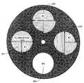
【0038】
結晶の複屈折を検出する上述の方法はまた、図6に示された回転リング200を使用して実施されることもできる。このようにして、図1の偏光子102は、リング200によって置換される。偏光計パラメータを検出するための図1を参照して上述された測定を実施するために、リング200が回転されて位置1の偏光子201が開口28を通過してビーム分割器45に至る照明ビームの経路内に入る。照明開口は、第1象限106aおよび第4象限106bから構成されており、そしてウェハ3からの反射は第2および第3象限の開口を通して集められる。図4B、図6Bの第1象限106aを遮断すなわちカバーすることが望ましい場合、位置2における偏光子202が開口ミラー28とビーム分割器45の間の放射線ビームの経路内に入るまでリング200が回転される。照明開口は第4象限106bのみから構成され、ウェハ3からの反射は第2象限の開口106cのみを通して集められる。代わって第4象限106bを遮断すなわちカバーすることが望ましい場合、位置3における偏光子203が光路内に入るまでリング200が回転される。照明開口は第1象限106aのみから構成され、ウェハ3からの反射は第3象限の開口106dのみを通して集められる。米国特許第5,747,813号と同じように操作することが望ましい場合には、偏光子が無い位置4にある開口204が、開口ミラー28とビーム分割器45の間のビームの光路内に入るまでリング200が回転される。
【0039】
上述の実施例においては、複屈折検出は異なる照明開口を使用して実現されたけれども、本質的には、代わりに集光開口を使用しても同じ結果が得られる。換言すれば、照明放射ビームの経路内における照明開口を部分的に遮蔽する代わりに、試料から反射され、そして集められて分光器と検出器へ導かれる放射線の経路内にある集光開口が部分的に遮蔽されすなわちカバーされる。このようなまたは他の改変例も本発明の範囲内に含まれる。
【0040】
複屈折を検出するためのシステム8を使用する適用例が上述されている。システム8はまた、試料表面の他のパラメータを検出するためにも使用できる。図面、特に図3Aおよび図3Bに関連する上述の式と説明とから、フォトダイオードアレー72の分光計によって検出される反射スペクトルは、Δに関する情報、偏光解析に一般に使用されかつ厚さに関連する偏光計パラメータ、および試料表面の薄膜の厚さと屈折率とを使用している。従って、試料表面の所定の様相が既知であれば、このような既知の様相は、システム8によって測定された偏光計パラメータに関する情報と結びつけられて、膜厚や屈折率のような試料の有用な情報を導出する。
【0041】
好適な実施例において、フォトダイオードアレー72によって得られる反射スペクトルは、フォトダイオードアレー74からの参照スペクトルと対比されて偏光計パラメータを導出し、SN比を改善する。しかしながら、幾つかの適用例においては、偏光計パラメータは参照スペクトルを使用せずに反射スペクトルのみから導出される。かかる適用においては、参照ビーム48は必要とされないから、ビーム48の生成に関連する全ての要素と参照スペクトルは図1および図2から削除される。このようなまたは他の改変は本発明の範囲内にある。
【0042】
図1の複合装置の分光学的偏光解析装置300が次に説明される。図1に示されるように、キセノンアークランプ10から発生し、焦点18、20を貫通通過した放射線の一部は、ビーム分割器302によって光ファイバケーブル304へ偏向され、これはコリメータ306へ放射線を供給する。平行にされた後、ビームは、偏光子310によって偏光化され、焦点ミラー312によってウェハ3へ集束される。その様なビームの反射は、収集ミラー314により集められ、そして屈曲ミラー316により分析器320を通して反射されてから検出のために分光計322と検出器324へ供給される。ウェハ3における反射によって生起されるビーム308の偏光状態の変化の値と相が測定できるように、偏光子310と分析器320とが互いに関して回転される。分光学的偏光解析装置300の操作の詳細な説明については、米国特許第5,608,526号を参照されたい。
【0043】
複数層の薄膜を持つ試料を測定するために、図1に示すように偏光計パラメータを測定するためのシステム8と分光学的偏光解析装置300とを有する複合装置を使用するのが望ましい。システム8と分光学的偏光解析装置300とは、サンプルビーム46とサンプルビーム308とがウェハ3の同じスポットに実質的に集束するように配置される。システム8によって測定される偏光計パラメータは、膜厚や膜の屈折率のような役に立つ情報を得るために、システム300によって測定される偏光解析装置パラメータと組み合わせられる。システム8によって測定される偏光計パラメータと、システム300を使用して得られる偏光解析装置パラメータとは、イワン オーリダル(Ivan OHLIDAL)とフランテスク ルケス(Frantisek LUKES) の「入射偏光解析の液浸と多重角との組合せによる極薄膜の自然酸化物層を備えた半導体の分析」(応用表面科学第35号(1988−1989)第259頁乃至273頁、北オランダ、アムステルダム)に記載されているような技術を使用して結合される。
【0044】
分光学的偏光解析装置のスペクトル領域は、約193nmのような深紫外までは延びないけれども、複合装置を使用することにより、かかる波長における屈折率を精確に測定することが可能である。このようにして、複合装置は分光学的偏光解析装置と偏光計システム8との複合スペクトルの全体に亘って屈折率を測定するために使用される。複合装置とシステム8および分光学的偏光解析装置の双方のデータとを使用することによって、分光学的偏光解析装置のスペクトル中の波長における、試料の異なる膜の厚さと屈折率とが見い出すことができる。この厚さ情報は、複合装置からのデータと一緒に、深紫外領域における膜の屈折率の発見に使用される。アレー72、74の検出器の数および分光器322の検出器324は、最適結果を得るための望ましい波長におけるデータを得るように選択される。
【0045】
代替実施例において、サンプルビーム46、308は、ウェハ3の同じ点に集束される必要性は無い。ウェハ3は、通常の方法による回転により、または直線状平行移動、または2つの運動の組合せにより、動かされるので、システム8によって測定される点は、引き続きシステム300によって測定され、またこの反対手順でも行われ、そして同じ点を測定する2つのシステムによって得られたデータが、上述したのと同様の要領で組み合わせられる。回転運動および平行移動運動は制御されるから、2つのシステム8、300によって測定されている点の相対運動は相関されることができる。
【0046】
上述したように、分光学的偏光解析装置は偏光計システム8と完全に結合されるが、システム8を単一波長偏光解析装置と連結することも可能である。この目的のために、図1の配置は分光器322の光路中においてミラー321と検出器324の間で回折格子を取り除くことによって簡単に改変される必要がある。偏光計スペクトル中の波長を持つレーザが、単一波長偏光解析装置のための放射源として使用されうる。単一波長偏光解析装置による測定およびシステム8による測定を用いて、偏光計スペクトルの全体に亘る波長における膜厚と屈折率とを得ることがなお可能である。
【0047】
本発明は種々の実施例を参照して以上に説明されたけれども、添付の請求項およびその均等によってのみ限定される本発明の範囲から逸脱することなしに変更または修正がなされうることを理解すべきである。
【図面の簡単な説明】
【図1】 本発明の好適な実施例を示すための、分光学的偏光解析装置と偏光計システムとを有する複合装置の概念図である。
【図2】 図1の偏光計システムの斜視図である。
【図3A】 偏光計パラメータを測定するための図1のシステムの一部分を示す簡略概念図である。
【図3B】 図2Aの照明開口のグラフ表示である。
【図4】 本発明の別の実施例を示すための、偏光計パラメータを測定するためのシステムの一部の簡略概念図である。
【図5A】 図1の偏光計パラメータ測定システムの簡略概念図であり、照明ビームおよび反射ビームの光路が開口を通過して、本発明の好適な実施例を示している。
【図5B】 試料の複屈折軸に関する図5Aの開口の概念図であり、本発明を示している。
【図6】 4個の異なった開口を備えたリングの概念図であり、その3個の開口は本発明の好適な実施例を示すためにその中に偏光子を有している。[0001]
BACKGROUND OF THE INVENTION
This invention relates generally to non-destructive techniques for measuring the surface properties of a sample, and more particularly to a system for measuring the polarimeter spectrum and other properties of a sample.
[0002]
[Prior art]
For many industrial applications, it is useful to measure the surface parameters of the sample, such as the thickness of the thin film and its refractive index. These parameters can be measured by a number of techniques. Among the well-known nondestructive inspection techniques are spectral reflection analysis and spectroscopic ellipsometry.
[0003]
In spectroscopic reflection analysis, an incident radiation beam is reflected from a sample, and the intensity of the reflected radiation is analyzed to determine the properties of the sample. Since incident radiation contains multiple wavelength components, a spectrum of measurement data (known as a reflectance spectrum or a relative reflectance spectrum) is measured. US Pat. No. 5,747,813 describes a type of broadband spectroreflectometer, which is hereby incorporated by reference in its entirety.
[0004]
A spectroscopic ellipsometer is described in US Pat. No. 5,608,526, which is hereby incorporated by reference in its entirety. As described in this patent, an incident radiation beam having a known polarization state is reflected from the sample at a generally large angle of incidence, and the polarization of the reflected radiation is analyzed to determine the properties of the sample. Since the polarization of the reflected radiation is different from that of the incident beam, quantitative and phase changes in the polarization state are measured to determine the thickness and refractive index of the thin film on the sample surface.
[0005]
Spectral reflection analysis is simpler and less expensive than spectroscopic ellipsometry, but spectroscopic ellipsometry is more accurate and more sensitive to surface properties than spectral reflection analysis. Spectral reflection analysis and spectroscopic ellipsometry are useful non-destructive inspection techniques, but it is difficult to measure certain surface parameters such as surface birefringence.
[0006]
Accordingly, it would be desirable to provide an improved measurement system for measuring surface parameters such as birefringence. It would also be desirable to provide a polarimeter system that measures sample surface properties to complement the non-destructive inspection techniques described above.
[0007]
[Means for Solving the Problems]
The polarimeter system proposed by the applicant maintains the simplicity of a spectroreflectometer, but has the same sensitivity to surface properties as a spectroscopic ellipsometer. A polarized sample beam of broadband radiation is focused on the sample surface and the radiation modified by the sample is collected. The sample beam focused on the sample has a number of polarization states. The radiation modified by the sample is analyzed with respect to the plane of polarization to produce a polarimeter spectrum. Information on the thickness and refractive index is obtained from the spectrum. Preferably, the polarization of the sample beam is changed only by focusing and the sample, and the analysis is performed with respect to a fixed polarization plane.
[0008]
In the preferred embodiment, focusing of the sample beam and collection of the modified radiation is repeated using two different apertures to detect the presence or absence of a birefringence axis in the sample. In other embodiments, the techniques described above are combined with ellipsometry to measure thin film thickness and refractive index.
[0009]
DETAILED DESCRIPTION OF THE INVENTION
For the sake of simplicity in illustration, the same members are denoted by the same reference numerals.
FIG. 1 is a schematic diagram of a composite device having a spectroscopic ellipsometer and a polarimeter system to illustrate a preferred embodiment of the present invention. Before describing the composite spectroscopic ellipsometer, the
[0010]
The overall optical arrangement of the
[0011]
A legend for showing the sample path, reference path, area illumination path, measurement illumination path, and ellipsometer path is shown in the upper right corner of FIG. As mentioned above, the overall optical arrangement of the system for measuring polarimeter parameters is described below with reference to FIGS.
[0012]
1 and 2 each show the same embodiment of an optical system according to the invention for measuring polarimeter parameters. The focusing member and other optical members of the
[0013]
The illumination system provides a
[0014]
The eccentric
[0015]
The other part of the
[0016]
The
[0017]
FIG. 1 shows the reflectometer and the observation and autofocus subsystems of the
[0018]
Several magnifications are possible for the
[0019]
The measurement of the relative reflectance spectrum of the
[0020]
The
[0021]
Since the
[0022]
The focal length of the
[0023]
The
[0024]
The relative reflectance spectrum is then simply obtained by dividing the sample light intensity at each wavelength by the relative reference intensity at each wavelength. Typically, this includes 512 division calculations where a 512-diode linear photodiode array is used to record the sample and reference spectra. In a preferred embodiment, the spectrum ranges from about 190 nm to 800 or 830 nm.
[0025]
In an embodiment of the present invention, the
[0026]
The
[0027]
Because of the innovative arrangement of optical elements used to measure the relative reflectance spectrum, many elements of the spectral measurement subsystem are also used in the autofocus subsystem. For example, since the relative reflectance spectrum measurement of the illustrated embodiment uses a
[0028]
The
[0029]
Referring to FIG. 3A, the
[0030]
From the above description, the
[0031]
The beam focused on the
[0032]
Φ toward the origin on the sample surfaceP Consider incident radiation from a
The detector current is expressed as:
[0034]
Some special cases are shown below.
A. φ0 = Π
From the above analysis, cos (Δ of the third term of the equations (4) and (6)o + Δs ) Coefficient is maximized when the polarizer and analyzer angles are the same, ie, when
[0036]
The polarimeter spectrum measured with respect to the detector current of
[0037]
[0038]
The above-described method of detecting crystal birefringence can also be implemented using the rotating ring 200 shown in FIG. In this way, the
[0039]
In the above embodiment, birefringence detection was realized using different illumination apertures, but essentially the same result is obtained using a condensing aperture instead. In other words, instead of partially shielding the illumination aperture in the path of the illumination radiation beam, there is a partial collection aperture in the path of radiation that is reflected from the sample and collected and directed to the spectrometer and detector. Shielded or covered. Such or other modifications are also included within the scope of the present invention.
[0040]
Applications using the
[0041]
In the preferred embodiment, the reflection spectrum obtained by the
[0042]
The
[0043]
In order to measure a sample with multiple layers of thin films, it is desirable to use a composite device having a
[0044]
Although the spectral region of the spectroscopic ellipsometer does not extend to deep ultraviolet, such as about 193 nm, the refractive index at such wavelengths can be accurately measured by using a composite device. In this way, the composite device is used to measure the refractive index throughout the composite spectrum of the spectroscopic ellipsometer and the
[0045]
In an alternative embodiment, the sample beams 46, 308 need not be focused to the same point on the
[0046]
As described above, the spectroscopic ellipsometer is fully coupled with the
[0047]
Although the invention has been described above with reference to various embodiments, it will be understood that changes or modifications can be made without departing from the scope of the invention which is limited only by the appended claims and equivalents thereof. Should.
[Brief description of the drawings]
FIG. 1 is a conceptual diagram of a composite apparatus having a spectroscopic ellipsometer and a polarimeter system for illustrating a preferred embodiment of the present invention.
FIG. 2 is a perspective view of the polarimeter system of FIG.
3A is a simplified conceptual diagram illustrating a portion of the system of FIG. 1 for measuring polarimeter parameters.
FIG. 3B is a graphical representation of the illumination aperture of FIG. 2A.
FIG. 4 is a simplified conceptual diagram of a portion of a system for measuring polarimeter parameters to illustrate another embodiment of the present invention.
5A is a simplified conceptual diagram of the polarimeter parameter measurement system of FIG. 1, showing the preferred embodiment of the present invention with the optical paths of the illumination beam and the reflected beam passing through the aperture.
FIG. 5B is a conceptual diagram of the aperture of FIG. 5A with respect to the birefringence axis of the sample, illustrating the present invention.
FIG. 6 is a conceptual diagram of a ring with four different apertures, the three apertures having polarizers therein for illustrating the preferred embodiment of the present invention.
Claims (72)
Translated fromJapanese広帯域放射線の、多数の偏光状態を有する偏光サンプルビームを試料上に集束するステップで、前記偏光サンプルビームを生成するために広帯域放射線のビームを偏光するステップをさらに含み、多数の偏光状態を有するビームを前記試料上に集束するように前記集束するステップが前記偏光サンプルビームを集束し、前記偏光状態が試料表面に直角な参照面に対する角度φの関数であるステップと、
前記試料により変化している前記偏光サンプルビームから放射線を集めるステップと、偏光計スペクトルを生成するために前記試料により変化しかつ前記試料から集められた放射線を偏光素子と分散により分析するステップであって、前記放射線と前記偏光サンプルビームとの間の偏光状態における実質的な相対的変化が、前記集束するステップ、前記集めるステップ、および前記分析するステップにおいて使用される光学素子間の相対運動によって引き起こされない、分析するステップと、
前記偏光計スペクトルから前記試料の光学的に検出可能な特性を導出するステップと、 を含む方法。A method for measuring a property of a sample, comprising:
Focusing a polarized sample beam of broadband radiation having a number of polarization states onto a sample, the method furthercomprising polarizing the beam of broadband radiation to generate the polarized sample beam, the beam having a number of polarization states Focusing the polarized sample beam to focus on the sample, the polarization state being a function of an angle φ relative to a reference plane perpendicular to the sample surface;
A step of collecting radiation from said polarization sample beam are more changesto thespecimen analysis by dispersing more varied and polarizing element radiation collected from the samplein thespecimen to generate a polarimeter spectrum A substantial relative change in polarization state between the radiation and the polarized sample beam between the optical elements used in the focusing step, the collecting step, and the analyzing step. Analyzing, not caused by relative movement;
Deriving an optically detectable property of the sample from the polarimeter spectrum.
広帯域放射線のビームを前記偏光サンプルビームと参照ビームとに分割するステップをさらに含み、前記集束するステップが前記偏光サンプルビームを前記試料上に集束する方法。The method of claim 1, wherein
The method further comprises splitting a beam of broadband radiation into the polarized sample beam and a reference beam, wherein the focusing step focuses the polarized sample beam onto the sample.
参照スペクトルを生成するために前記参照ビームを検出するステップをさらに含み、前記導出するステップが膜厚および屈折率情報を導出するために前記偏光計スペクトルと前記参照スペクトルとを対比する方法。The method of claim 2, wherein
Detecting the reference beam to generate a reference spectrum, the deriving step comparing the polarimeter spectrum with the reference spectrum to derive film thickness and refractive index information.
前記参照ビーム、前記偏光計スペクトル、および前記参照スペクトルが、約190nmから約830nmまでの範囲の多重波長を含む方法。The method of claim 3, wherein
The method wherein the reference beam, the polarimeter spectrum, and the reference spectrum comprise multiple wavelengths ranging from about 190 nm to about 830 nm.
前記分割するステップが、前記広帯域放射線のビームを完全に横切る程でないように置かれたミラーに前記広帯域放射線のビームを導くことを含む方法。The method of claim 2, wherein
The method comprising the step of directing the beam of broadband radiation to a mirror positioned so as not to completely traverse the beam of broadband radiation.
前記分割するステップが前記広帯域放射線のビームの一部をサンプルビームに偏向することを含み、前記放射線の非偏向部分が参照放射線ビームを画成する方法。The method of claim 2, wherein
The splitting includes deflecting a portion of the beam of broadband radiation into a sample beam, and the undeflected portion of the radiation defines a reference radiation beam.
前記導出するステップが、複屈折特性、膜厚または屈折率情報を導出する方法。The method of claim 1, wherein
The deriving step derives birefringence characteristics, film thickness or refractive index information.
前記集束するステップおよび前記集めるステップが、共通の対物レンズを使用する方法。The method of claim 1, wherein
The method in which the focusing and collecting steps use a common objective lens.
前記試料が1以上の複屈折軸を有し、前記集束するステップまたは前記集めるステップが前記複屈折軸のうちの1つの複屈折軸の周りに中心化された開口を使用する方法。The method of claim 1, wherein
The method wherein the sample has one or more birefringent axes and the focusing or collecting step uses an aperture centered about one of the birefringent axes.
前記集束するステップおよび前記集めるステップを、前記複屈折軸のうちの少なくとも2つの複屈折軸の周りにそれぞれ整列された少なくとも2つの異なる開口を使用して繰り返す方法。The method of claim9 , wherein
The method of repeating the focusing and collecting steps using at least two different apertures respectively aligned about at least two of the birefringent axes.
前記集束するステップおよび前記集めるステップを、前記複屈折軸のうちの少なくとも2つの複屈折軸の周りにそれぞれ中心化された少なくとも2つの異なる開口を使用して繰り返す方法。The method of claim10 , wherein:
The method of repeating the focusing and collecting steps using at least two different apertures, each centered around at least two of the birefringent axes.
前記集束するステップおよび前記集めるステップを、前記試料内の複屈折軸の存否を検出するために2つの異なる開口を使用して繰り返す方法。The method of claim 1, wherein
A method of repeating the focusing and collecting steps using two different apertures to detect the presence or absence of a birefringence axis in the sample.
前記偏光計スペクトルが、約190nmから約830nmまでの範囲の多重波長を含む方法。The method of claim 1, wherein
The method, wherein the polarimeter spectrum comprises multiple wavelengths ranging from about 190 nm to about 830 nm.
前記分析するステップが、前記試料により変化した放射線をあらかじめ設定された固定の偏光面に対して分析する方法。The method of claim 1, wherein
Wherein said analyzing step comprises analyzing against preset polarization plane of the fixed more varied radiationin thespecimen.
前記分析するステップの前に、前記試料により変化しかつ前記試料から集められた放射線の位相を変更するステップをさらに含む方法。The method of claim 1, wherein
The method prior to the step, further comprising the step of changing a more varied and the phase of the radiation collected from the samplein thespecimen to the analysis.
前記変更するステップが、前記試料により変化しかつ前記試料から集められた放射線の位相を約π/4だけ遅延する方法。The method of claim15 , wherein
How the step of changing is delayed more varied and the phase of the radiation collected from the sampleinto thespecimen by about [pi / 4.
前記集束するステップおよび前記集めるステップが、2回行われ、かつ試料表面に直角な参照面に対する2つの異なる角度範囲内で行われる方法。The method of claim 1, wherein
The method wherein the focusing and collecting steps are performed twice and are performed within two different angular ranges relative to a reference plane perpendicular to the sample surface.
前記集束するステップおよび前記集めるステップが、放射線を2つの異なる開口のセットを通して通過させることによって2回行われる方法。The method of claim 1, wherein
The method wherein the focusing and collecting steps are performed twice by passing radiation through two different sets of apertures.
前記2つの異なる開口が、回転により実質的に90°離れている方法。The method of claim18 , wherein:
The method wherein the two different openings are substantially 90 ° apart by rotation.
前記試料が少なくとも2つの複屈折軸に沿った種々の光学的に検出可能な特性を有し、前記集束するステップまたは前記集めるステップが前記複屈折軸のうちの1つの複屈折軸の周りに中心化された開口を使用する方法。The method of claim 1, wherein
The sample has various optically detectable properties along at least two birefringence axes, and the focusing or collecting step is centered about one of the birefringence axes To use a standardized aperture.
前記集束するステップおよび前記集めるステップを、前記複屈折軸のうちの少なくとも2つの複屈折軸の周りにそれぞれ整列された少なくとも2つの異なる開口を使用して繰り返す方法。The method of claim20 , wherein
The method of repeating the focusing and collecting steps using at least two different apertures respectively aligned about at least two of the birefringent axes.
前記サンプルビームが第2の偏光素子により前記試料に達する前に、前記サンプルビームを偏光するステップをさらに含み、前記試料が少なくとも2つの複屈折軸に沿った種々の光学的に検出可能な特性を有し、前記集束するステップ、前記集めるステップ、前記分析分散するステップ、および前記導出するステップが少なくとも2回行われる間は、前記第2の偏光素子が前記複屈折軸のうちの1つに整列される方法。The method of claim 1, wherein
Before thesample beam reaches the sample by the second polarizing element, wherein the sample beam further comprises the step of polarizing the various optically detectable property which said sample along at least two birefringent axes And the second polarizing element is placed on one of the birefringence axes while the focusing step, the collecting step, the analyzing and dispersing step, and the deriving step are performed at least twice. How to be aligned.
前記集束するステップ、前記集めるステップ、前記分析分散するステップ、および前記導出するステップが少なくとも2回行われる間は、前記第2の偏光素子が回転により実質的に90°離れている2つの異なる位置にある方法。The method of claim22 , wherein
While the focusing step, the collecting step, the analyzing and dispersing step and the deriving step are performed at least twice, the two different positions where the second polarizing element is substantially 90 ° apart by rotation. The way it is.
前記サンプルビームが第2の偏光素子により前記試料に達する前に、前記サンプルビームを偏光するステップをさらに含み、前記集束するステップ、前記集めるステップ、前記分析するステップ、および前記導出するステップが、前記偏光素子が異なる位置にある状態で少なくとも2回行われる方法。The method of claim 1, wherein
Before thesample beam reaches the sample by the second polarizing element, wherein the sample beam further comprises the step of polarizing a step of focusing the collected step, step of analyzing, and said step of deriving is The method is performed at least twice with the polarizing elements in different positions.
前記集束するステップ、前記集めるステップ、前記分析するステップ、および前記導出するステップが少なくとも2回行われる間は、前記偏光するステップおよび前記分析するステップで使用される前記偏光素子が実質的に同じ偏光面を有する方法。25. The method of claim24 , wherein
While the focusing, collecting, analyzing, and deriving steps are performed at least twice, the polarizing elements used in the polarizing step and the analyzing step are substantially the same polarization. A method having a surface.
前記集束するステップ、前記集めるステップ、および前記分析するステップが少なくとも2回行われる間は前記分散するステップが少なくとも2つのスペクトルを生成し、前記導出するステップが前記少なくとも2つのスペクトルを使用して前記試料の複屈折特性に関する情報を導出する方法。25. The method of claim24 , wherein
While the focusing, collecting, and analyzing steps are performed at least twice, the dispersing step generates at least two spectra, and the deriving step uses the at least two spectra. A method for deriving information on the birefringence characteristics of a sample.
前記2つの異なる位置が、回転により実質的に90°離れている方法。25. The method of claim24 , wherein
The method wherein the two different positions are substantially 90 ° apart by rotation.
前記集束するステップが前記偏光サンプルビームを形成するためにビームを偏光することを含み、前記ビームを偏光することと前記試料により変化しかつ前記試料から集められた放射線を分析するステップとが前記偏光素子によって行われる方法。The method of claim 1, wherein
The method comprising polarizing the beam to said step of focusing to form the polarizing sample beam, and a step of analyzing a more varied radiation and collected from the sampleto saidspecimen to polarize the beam A method performed by the polarizing element.
前記広帯域放射線のサンプルビームが、紫外線波長または深紫外線波長を少なくとも1つ含む方法。The method of claim 1, wherein
The method wherein the broadband radiation sample beam comprises at least one ultraviolet wavelength or deep ultraviolet wavelength.
前記試料により変化しかつ前記試料から集められた放射線を分散するステップが、前記試料の偏光解析装置のパラメータΔに関する情報を含むスペクトルを生成する方法。The method of claim 1, wherein
How the step of dispersing a more varied radiation and collected from the samplein thespecimen produces a spectrum that contains information about the parameters Δ of the polarization analyzer of the sample.
広帯域放射線のビームを供給する放射線源と、
広帯域放射線の多数の偏光状態を有する偏光サンプルビームを試料上に集束する手段であって、前記広帯域放射線のビームを前記偏光サンプルビームと参照ビームとに分割する手段をさらに備え、前記集束された偏光サンプルビームが多数の偏光状態を有するように前記集束する手段が前記偏光サンプルビームを前記試料上に集束し、前記偏光状態が試料表面に直角な参照面に対する角度φの関数である集束する手段と、
前記試料により変化している前記偏光サンプルビームから放射線を集める手段と、
偏光計スペクトルを生成するために前記試料により変化しかつ前記試料から集められた放射線を偏光素子と分散を含んで分析する手段であって、前記放射線と前記偏光サンプルビームとの間の偏光状態における実質的な相対的変化が、前記集束する手段、前記集める手段、および前記分析する手段において使用される光学素子間の相対運動によって引き起こされない、分析する手段と、
前記偏光計スペクトルから前記試料の光学的に検出可能な特性を導出する手段と、
を備える装置。An apparatus for measuring the characteristics of a sample,
A radiation source supplying a beam of broadband radiation;
Meansfor focusing a polarized sample beam having multiple polarization states ofbroadband radiation onto a sample, the means further comprising means for splitting the beam of broadband radiation into the polarized sample beam and a reference beam; Means for focusing such that the sample beam has a number of polarization states to focus the polarized sample beam on the sample, the focusing state being a function of an angle φ relative to a reference plane perpendicular to the sample surface ; ,
Means for collecting radiation from the polarizing sample beam are more changesto thespecimen,
And means for analyzing include dispersion and polarization element radiation collected from more varied and the sampleto thespecimen in order to generate a polarimeter spectrum, polarization between the polarization sample beam and the radiation Means for analyzing, wherein a substantial relative change in state is not caused by relative movement between optical elements used in said means for focusing, means for collecting and means for analyzing;
Means for deriving optically detectable properties of the sample from the polarimeter spectrum;
A device comprising:
前記分割する手段が、前記広帯域放射線のビームを完全に横切る程でないように置かれた全反射ミラーを含む装置。32. The apparatus of claim31 , wherein
An apparatus comprising a total reflection mirror positioned so that the means for splitting is not completely traversing the beam of broadband radiation.
前記分割する手段が、前記放射線源からの広帯域放射線のビームの一部をサンプルビームに偏向し、前記放射線の非偏向部分が参照放射線ビームを画成する装置。32. The apparatus of claim31 , wherein
An apparatus in which the means for splitting deflects a portion of a beam of broadband radiation from the radiation source into a sample beam and an undeflected portion of the radiation defines a reference radiation beam.
参照スペクトルを生成するために前記参照ビームを検出する検出器をさらに備え、前記導出する手段が膜厚と屈折率情報を導出するために前記偏光計スペクトルと前記参照スペクトルとを対比する手段を含む装置。32. The apparatus of claim31 , wherein
A detector for detecting the reference beam to generate a reference spectrum, wherein the means for deriving includes means for comparing the polarimeter spectrum and the reference spectrum to derive film thickness and refractive index information; apparatus.
前記放射線ビーム、前記偏光計スペクトル、および前記参照スペクトルが、約190nmから約830nmまでの範囲の多重波長を含む装置。35. The apparatus of claim34 .
The apparatus wherein the radiation beam, the polarimeter spectrum, and the reference spectrum comprise multiple wavelengths ranging from about 190 nm to about 830 nm.
前記分割する手段が、偏光ビーム分割器を含む装置。32. The apparatus of claim31 , wherein
The apparatus wherein the means for splitting comprises a polarizing beam splitter.
前記分割する手段が、ビーム分割器を含む装置。32. The apparatus of claim31 , wherein
The apparatus wherein the means for splitting comprises a beam splitter.
前記偏光素子が、前記集束する手段の光路内にある装置。32. The apparatus of claim31 , wherein
Apparatus in which the polarizing element is in the optical path of the means for focusing.
前記導出する手段が、複屈折特性、膜厚または屈折率情報を導出する装置。32. The apparatus of claim31 , wherein
An apparatus in which the means for deriving derives birefringence characteristics, film thickness or refractive index information.
前記偏光サンプルビームを形成するために広帯域放射線のビームを通過する偏光子をさらに備え、前記集束する手段による集束および前記分析分散する手段による分析中に前記偏光子と前記偏光素子とは互いに関連して回転しない装置。32. The apparatus of claim31 , wherein
A polarizer that passes a beam of broadband radiation to form the polarized sample beam, the polarizer and the polarizing element being associated with each other during focusing by the focusing means and analysis by the analyzing and dispersing means; A device that does not rotate.
前記集束する手段および前記集める手段が、前記偏光サンプルビームを前記試料上に集束しかつ前記試料により変化した放射線を集める共通の対物レンズを有する装置。32. The apparatus of claim31 , wherein
The converging to means and said collecting means, devices having a common objective lens to collect more varied radiation the polarization sample beamto focused and thespecimen on the specimen.
偏光されたかまたは偏光されない前記サンプルビームを生成するために、放射線源からの広帯域放射線のビームの経路の内外に偏光素子を動かす手段をさらに備える装置。32. The apparatus of claim31 , wherein
An apparatus further comprising means for moving a polarizing element in and out of a path of a beam of broadband radiation from a radiation source to generate the sample beam that is polarized or unpolarized.
前記偏光素子が、前記放射線源から発生するビームを偏光し、前記試料により変化しかつ前記集める手段により集められた放射線を分析する装置。43. The apparatus of claim42 .
The polarizing element polarizes the beam generated from the radiation source, analyzing the radiation collected by the more varied and the collecting meansto thespecimen device.
放射線源をさらに備え、前記集束する手段が前記放射線源からの放射線を1以上の複屈折軸を有する前記試料上に集束し、前記装置が前記複屈折軸のうちの1つの複屈折軸に整列される少なくとも1つの開口を備え、前記開口が前記放射線源と前記分析する手段との間の光路内にある装置。32. The apparatus of claim31 , wherein
And further comprising a radiation source, wherein the means for focusing focuses radiation from the radiation source onto the sample having one or more birefringence axes, and the apparatus aligns with one of the birefringence axes. Wherein the opening is in the optical path between the radiation source and the means for analyzing.
前記少なくとも1つの開口が、前記複屈折軸のうちの1つの複屈折軸の周りに中心化される装置。45. The apparatus of claim44 .
The apparatus wherein the at least one aperture is centered about one of the birefringent axes.
前記複屈折軸のうちの1つの複屈折軸に整列される少なくとも2つの開口のうちの1つを選択する手段をさらに備える装置。45. The apparatus of claim44 .
Apparatus further comprising means for selecting one of at least two apertures aligned with one of the birefringence axes.
前記選択する手段により2つの異なる開口のそれぞれを前記複屈折軸の対応する一つに整列させるので、前記2つの異なる開口がそれらの対応する複屈折軸に連続して整列されたときに得られる偏光計スペクトルが、前記試料の複屈折に関する情報をもたらす装置。The apparatus of claim46 .
The means for selecting aligns each of two different apertures with a corresponding one of the birefringence axes, so that the two different apertures are obtained when they are successively aligned with their corresponding birefringence axes. An apparatus in which a polarimeter spectrum provides information about the birefringence of the sample.
前記選択する手段が、内部に少なくとも2つの開口を備えたリングを含む装置。48. The apparatus of claim47 .
The apparatus wherein the means for selecting includes a ring with at least two openings therein.
前記リングが、前記少なくとも2つの開口のそれぞれに偏光子を有する装置。49. The apparatus of claim48 .
The apparatus wherein the ring has a polarizer in each of the at least two openings.
前記少なくとも2つの開口のうちの2つが、1個の象限が遮蔽された円の形に実質的に成形される装置。49. The apparatus of claim48 .
An apparatus wherein two of the at least two openings are substantially shaped into a circle with one quadrant shielded.
放射線源をさらに備え、前記集束する手段が前記放射線源からの放射線を1以上の複屈折軸を有する前記試料上に集束し、前記装置が前記複屈折軸を検出するために前記サンプルビームの光路内で線状偏光子を回転させる手段をさらに備える装置。32. The apparatus of claim31 , wherein
And further comprising a radiation source, wherein the focusing means focuses the radiation from the radiation source onto the sample having one or more birefringence axes, and the apparatus detects an optical path of the sample beam for detecting the birefringence axis. The apparatus further comprising means for rotating the linear polarizer within.
前記広帯域放射線が、約190nmから約830nmまでの範囲の多重波長を含む装置。32. The apparatus of claim31 , wherein
The apparatus, wherein the broadband radiation comprises multiple wavelengths ranging from about 190 nm to about 830 nm.
前記分析する手段が、前記試料により変化した放射線をあらかじめ設定された固定の偏光面に対して分析する装置。32. The apparatus of claim31 , wherein
It said means for analyzing is analyzed with respect to preset polarization plane of the fixed more varied radiationin thespecimen device.
前記集める手段と前記分析する手段との間の光路内に位相遅延器をさらに備え、前記位相遅延器が、前記分析する手段の前に、前記試料により変化しかつ前記試料から集められた放射線の位相を変更する装置。32. The apparatus of claim31 , wherein
Further comprising a phase retarder in the optical path between the means of analyzing said collecting means, the phase retarder is in front of the means for analyzing, collected from more varied and the sampleto thespecimen A device that changes the phase of radiation.
前記位相遅延器が、前記試料により変化しかつ前記試料から集められた放射線の位相を約π/4遅延させる装置。56. The apparatus of claim54 .
Apparatus wherein the phase delayer is, by about [pi / 4 delay more varied and the phase of the radiation collected from the sampleinto thespecimen.
前記集束する手段または前記集める手段が、反射された放射線の位相において、前記集束する手段および前記集める手段により約π/2の総変換を導入するコーティングを有するミラーを含む装置。32. The apparatus of claim31 , wherein
Apparatus wherein the means for focusing or the means for collecting comprises a mirror having a coating that introduces a total transformation of about π / 2 by the means for focusing and the means for collecting in the phase of the reflected radiation.
前記集束する手段および前記集める手段が、2回行われ、かつ試料表面に直角な参照面に対する2つの異なる角度範囲内で行われる装置。32. The apparatus of claim31 , wherein
An apparatus in which the means for focusing and the means for collecting are performed twice and within two different angular ranges relative to a reference plane perpendicular to the sample surface.
前記集束する手段および前記集める手段が、放射線を2つの異なる開口のセットを通して通過させることによって2回行われる装置。32. The apparatus of claim31 , wherein
Apparatus wherein said means for focusing and means for collecting are performed twice by passing radiation through two different sets of apertures.
前記2つの異なる開口のセットが、回転により実質的に90°離れている装置。59. The apparatus of claim58 , wherein
A device in which the two different sets of openings are substantially 90 ° apart by rotation.
前記試料が少なくとも2つの複屈折軸に沿った種々の光学的に検出可能な特性を有し、前記装置が、放射線を集束しかつ放射線を集めるために、前記複屈折軸のうちの1つの複屈折軸の周りに中心化された開口をさらに備える装置。32. The apparatus of claim31 , wherein
The sample has various optically detectable properties along at least two birefringence axes, and the device is capable of collimating one of the birefringence axes to focus and collect the radiation. The apparatus further comprising an aperture centered about the refractive axis.
放射線を集束しかつ放射線を集めるために、前記複屈折軸のうちの少なくとも2つの複屈折軸の周りにそれぞれ整列された少なくとも2つの異なる開口をさらに備える装置。59. The apparatus of claim58 , wherein
An apparatus further comprising at least two different apertures each aligned around at least two of the birefringent axes for focusing and collecting the radiation.
前記サンプルビームが前記試料に達する前に、前記サンプルビームを偏光する第2の偏光素子をさらに備え、前記試料が少なくとも2つの複屈折軸に沿った種々の光学的に検出可能な特性を有し、前記集束する手段、前記集める手段、前記分析分散する手段、および前記導出する手段が少なくとも2回行われる間は、前記第2の偏光素子が前記複屈折軸のうちの1つに整列される装置。32. The apparatus of claim31 , wherein
Before thesample beam reaches the sample, the sample beam further comprises a second polarizing element for polarizing, have a variety of optically detectable property which said sample along at least two birefringent axes The second polarizing element is aligned with one of the birefringence axes while the means for focusing, the means for collecting, the means for analyzing and dispersing, and the means for deriving are performed at least twice. Equipment.
前記集束する手段、前記集める手段、前記分析する手段、および前記導出する手段が少なくとも2回行われる間は、前記第2の偏光素子が回転により実質的に90°離れている2つの異なる位置にある装置。The apparatus of claim62 .
While the means for focusing, the means for collecting, the means for analyzing, and the means for deriving are performed at least twice, the second polarizing element is in two different positions that are substantially 90 ° apart by rotation. A device.
前記集束する手段、前記集める手段、および前記分散する手段が行われる少なくとも2つの異なる位置間で第2の偏光素子を動かす機器をさらに備える装置。The apparatus of claim62 .
An apparatus further comprising an apparatus for moving a second polarizing element between at least two different positions where the means for focusing, the means for collecting and the means for dispersing are performed.
前記サンプルビームが前記試料に達する前に、前記サンプルビームを偏光する第2の偏光素子をさらに備え、前記集束する手段、前記集める手段、前記分析する手段、および前記導出する手段が、前記偏光素子が異なる位置にある状態で少なくとも2回行われる装置。32. The apparatus of claim31 , wherein
Before thesample beam reaches the sample, the sample beam further comprises a second polarizing element for polarizing said means for focusing the collected means, the means for analyzing, and said means for deriving said polarization A device that is performed at least twice with the elements in different positions.
前記集束する手段、前記集める手段、前記分析する手段、および前記導出する手段が少なくとも2回行われる間は、前記サンプルビームを偏光することおよび前記分析する手段で使用される前記偏光素子が実質的に同じ偏光面を有する装置。68. The apparatus of claim65 .
While the means for focusing, the means for collecting, the means for analyzing, and the means for deriving are performed at least twice, the polarizing element used in the means for polarizing and analyzing the sample beam is substantially Having the same plane of polarization.
前記集束する手段、前記集める手段、前記分散する手段が行われる少なくとも2つの異なる位置間で第2の偏光素子を動かす機器をさらに備える装置。68. The apparatus of claim65 .
An apparatus further comprising an apparatus for moving the second polarizing element between at least two different positions where the means for focusing, the means for collecting, and the means for dispersing are performed.
前記集束する手段、前記集める手段、および前記分析する手段が少なくとも2回行われる間は前記分散する手段が少なくとも2つのスペクトルを生成し、前記導出する手段が前記少なくとも2つのスペクトルを使用して前記試料の複屈折特性に関する情報を導出する装置。68. The apparatus of claim65 .
While the means for focusing, the means for collecting, and the means for analyzing are performed at least twice, the means for dispersing generates at least two spectra, and the means for deriving uses the at least two spectra to An apparatus for deriving information on the birefringence characteristics of a sample.
前記2つの異なる位置が、回転により実質的に90°離れている装置。68. The apparatus of claim65 .
A device in which the two different positions are substantially 90 ° apart by rotation.
前記集束する手段が前記偏光サンプルビームを形成するためにビームを偏光し、前記ビームを偏光することと前記試料により変化しかつ前記試料から集められた放射線を分析する手段とが前記偏光素子によって行われる装置。32. The apparatus of claim31 , wherein
Polarized beam to said means for focusing to form the polarizing sample beam, said beam more changesto saidspecimen for polarizing and means for analyzing the radiation collected from said sample said polarizing element A device made by.
前記広帯域放射線のサンプルビームが、紫外線波長または深紫外線波長を少なくとも1つ含む装置。32. The apparatus of claim31 , wherein
An apparatus wherein the broadband radiation sample beam comprises at least one ultraviolet or deep ultraviolet wavelength.
前記分散する手段が、前記試料により変化しかつ前記試料から集められた放射線を分散して、前記試料の偏光解析装置のパラメータΔに関する情報を含むスペクトルを生成する装置。32. The apparatus of claim31 , wherein
The dispersed means to distribute the more varied and radiation collected from the samplein thespecimen, apparatus for generating a spectrum that contains information about the parameters Δ of the polarization analyzer of the sample.
Applications Claiming Priority (3)
| Application Number | Priority Date | Filing Date | Title |
|---|---|---|---|
| US09/246,922 | 1999-02-09 | ||
| US09/246,922US6184984B1 (en) | 1999-02-09 | 1999-02-09 | System for measuring polarimetric spectrum and other properties of a sample |
| PCT/US2000/003290WO2000047961A1 (en) | 1999-02-09 | 2000-02-09 | System for measuring polarimetric spectrum and other properties of a sample |
Related Child Applications (1)
| Application Number | Title | Priority Date | Filing Date |
|---|---|---|---|
| JP2011055357ADivisionJP4880791B2 (en) | 1999-02-09 | 2011-03-14 | System for measuring the polarimeter spectrum and other properties of a sample |
Publications (2)
| Publication Number | Publication Date |
|---|---|
| JP2002536657A JP2002536657A (en) | 2002-10-29 |
| JP4880122B2true JP4880122B2 (en) | 2012-02-22 |
Family
ID=22932784
Family Applications (2)
| Application Number | Title | Priority Date | Filing Date |
|---|---|---|---|
| JP2000598823AExpired - Fee RelatedJP4880122B2 (en) | 1999-02-09 | 2000-02-09 | System for measuring the polarimeter spectrum and other properties of a sample |
| JP2011055357AExpired - LifetimeJP4880791B2 (en) | 1999-02-09 | 2011-03-14 | System for measuring the polarimeter spectrum and other properties of a sample |
Family Applications After (1)
| Application Number | Title | Priority Date | Filing Date |
|---|---|---|---|
| JP2011055357AExpired - LifetimeJP4880791B2 (en) | 1999-02-09 | 2011-03-14 | System for measuring the polarimeter spectrum and other properties of a sample |
Country Status (3)
| Country | Link |
|---|---|
| US (3) | US6184984B1 (en) |
| JP (2) | JP4880122B2 (en) |
| WO (1) | WO2000047961A1 (en) |
Families Citing this family (153)
| Publication number | Priority date | Publication date | Assignee | Title |
|---|---|---|---|---|
| US6930813B1 (en) | 2000-04-25 | 2005-08-16 | J.A. Woollam Co. Inc. | Spatial filter source beam conditioning in ellipsometer and the like systems |
| US7489400B1 (en)* | 1995-09-20 | 2009-02-10 | J.A. Woollam Co., Inc. | System and method of applying xenon arc-lamps to provide 193 nm wavelengths |
| US6049220A (en)* | 1998-06-10 | 2000-04-11 | Boxer Cross Incorporated | Apparatus and method for evaluating a wafer of semiconductor material |
| US7042580B1 (en)* | 1999-02-01 | 2006-05-09 | Tokyo Electron Limited | Apparatus for imaging metrology |
| US7177019B2 (en)* | 1999-02-01 | 2007-02-13 | Tokyo Electron Limited | Apparatus for imaging metrology |
| US6804003B1 (en) | 1999-02-09 | 2004-10-12 | Kla-Tencor Corporation | System for analyzing surface characteristics with self-calibrating capability |
| US6184984B1 (en)* | 1999-02-09 | 2001-02-06 | Kla-Tencor Corporation | System for measuring polarimetric spectrum and other properties of a sample |
| US6323951B1 (en)* | 1999-03-22 | 2001-11-27 | Boxer Cross Incorporated | Apparatus and method for determining the active dopant profile in a semiconductor wafer |
| JP5248722B2 (en)* | 1999-04-22 | 2013-07-31 | ケーエルエー−テンカー コーポレイション | Surface characteristic analysis system with self-calibration function |
| US7468794B1 (en) | 1999-10-18 | 2008-12-23 | J.A. Woollam Co., Inc. | Rotating compensator ellipsometer system with spatial filter equivalent |
| DE19963345A1 (en)* | 1999-12-27 | 2001-07-05 | Leica Microsystems | Optical measuring arrangement and method for inclination measurement |
| US6590655B2 (en) | 2000-04-25 | 2003-07-08 | J.A. Woollam Co. Inc. | System and method of improving electromagnetic radiation beam characteristics in ellipsometer and the like systems |
| DE10021378A1 (en)* | 2000-05-02 | 2001-11-08 | Leica Microsystems | Optical measuring arrangement with an ellipsometer |
| FR2811761B1 (en)* | 2000-07-17 | 2002-10-11 | Production Rech S Appliquees | HIGH SPACE RESOLUTION ELLIPSOMETER OPERATING IN THE INFRARED |
| US7541201B2 (en) | 2000-08-30 | 2009-06-02 | Kla-Tencor Technologies Corporation | Apparatus and methods for determining overlay of structures having rotational or mirror symmetry |
| US7317531B2 (en)* | 2002-12-05 | 2008-01-08 | Kla-Tencor Technologies Corporation | Apparatus and methods for detecting overlay errors using scatterometry |
| US6891627B1 (en)* | 2000-09-20 | 2005-05-10 | Kla-Tencor Technologies Corp. | Methods and systems for determining a critical dimension and overlay of a specimen |
| US7130029B2 (en) | 2000-09-20 | 2006-10-31 | Kla-Tencor Technologies Corp. | Methods and systems for determining an adhesion characteristic and a thickness of a specimen |
| US7106425B1 (en) | 2000-09-20 | 2006-09-12 | Kla-Tencor Technologies Corp. | Methods and systems for determining a presence of defects and a thin film characteristic of a specimen |
| US6812045B1 (en) | 2000-09-20 | 2004-11-02 | Kla-Tencor, Inc. | Methods and systems for determining a characteristic of a specimen prior to, during, or subsequent to ion implantation |
| US6694284B1 (en) | 2000-09-20 | 2004-02-17 | Kla-Tencor Technologies Corp. | Methods and systems for determining at least four properties of a specimen |
| US6633831B2 (en) | 2000-09-20 | 2003-10-14 | Kla Tencor Technologies | Methods and systems for determining a critical dimension and a thin film characteristic of a specimen |
| US6919957B2 (en) | 2000-09-20 | 2005-07-19 | Kla-Tencor Technologies Corp. | Methods and systems for determining a critical dimension, a presence of defects, and a thin film characteristic of a specimen |
| US6782337B2 (en)* | 2000-09-20 | 2004-08-24 | Kla-Tencor Technologies Corp. | Methods and systems for determining a critical dimension an a presence of defects on a specimen |
| US6673637B2 (en) | 2000-09-20 | 2004-01-06 | Kla-Tencor Technologies | Methods and systems for determining a presence of macro defects and overlay of a specimen |
| US7349090B2 (en) | 2000-09-20 | 2008-03-25 | Kla-Tencor Technologies Corp. | Methods and systems for determining a property of a specimen prior to, during, or subsequent to lithography |
| US6831742B1 (en) | 2000-10-23 | 2004-12-14 | Applied Materials, Inc | Monitoring substrate processing using reflected radiation |
| US6911349B2 (en)* | 2001-02-16 | 2005-06-28 | Boxer Cross Inc. | Evaluating sidewall coverage in a semiconductor wafer |
| US6812717B2 (en)* | 2001-03-05 | 2004-11-02 | Boxer Cross, Inc | Use of a coefficient of a power curve to evaluate a semiconductor wafer |
| JP2002267418A (en)* | 2001-03-09 | 2002-09-18 | Horiba Ltd | Film thickness measuring instrument |
| WO2002079760A2 (en)* | 2001-03-30 | 2002-10-10 | Therma-Wave, Inc. | Polarimetric scatterometer for critical dimension measurements of periodic structures |
| US20030002043A1 (en) | 2001-04-10 | 2003-01-02 | Kla-Tencor Corporation | Periodic patterns and technique to control misalignment |
| US6782342B2 (en)* | 2001-06-08 | 2004-08-24 | University Of Maine | Spectroscopy instrument using broadband modulation and statistical estimation techniques to account for component artifacts |
| US6597463B1 (en) | 2001-06-13 | 2003-07-22 | Advanced Micro Devices, Inc. | System to determine suitability of sion arc surface for DUV resist patterning |
| US6940592B2 (en)* | 2001-10-09 | 2005-09-06 | Applied Materials, Inc. | Calibration as well as measurement on the same workpiece during fabrication |
| EP1446641A4 (en)* | 2001-10-15 | 2009-01-07 | Xiangdong Zhu | Methods and apparatus for measuring refractive index and optical absorption differences |
| US6982791B2 (en)* | 2001-12-19 | 2006-01-03 | Therma-Wave, Inc. | Scatterometry to simultaneously measure critical dimensions and film properties |
| US7050162B2 (en) | 2002-01-16 | 2006-05-23 | Therma-Wave, Inc. | Optical metrology tool having improved contrast |
| US7253901B2 (en) | 2002-01-23 | 2007-08-07 | Kla-Tencor Technologies Corporation | Laser-based cleaning device for film analysis tool |
| US6971791B2 (en)* | 2002-03-01 | 2005-12-06 | Boxer Cross, Inc | Identifying defects in a conductive structure of a wafer, based on heat transfer therethrough |
| US6958814B2 (en)* | 2002-03-01 | 2005-10-25 | Applied Materials, Inc. | Apparatus and method for measuring a property of a layer in a multilayered structure |
| US8013996B1 (en) | 2002-06-24 | 2011-09-06 | J.A. Woollam Co., Inc. | Spatial filter in sample investigation system |
| US7671989B2 (en)* | 2002-06-24 | 2010-03-02 | J. A. Woollam Co., Inc. | Information maintenance during intensity attenuation in focused beams |
| US7554662B1 (en) | 2002-06-24 | 2009-06-30 | J.A. Woollam Co., Inc. | Spatial filter means comprising an aperture with a non-unity aspect ratio in a system for investigating samples with electromagnetic radiation |
| US7869057B2 (en) | 2002-09-09 | 2011-01-11 | Zygo Corporation | Multiple-angle multiple-wavelength interferometer using high-NA imaging and spectral analysis |
| US7139081B2 (en) | 2002-09-09 | 2006-11-21 | Zygo Corporation | Interferometry method for ellipsometry, reflectometry, and scatterometry measurements, including characterization of thin film structures |
| US6878559B2 (en)* | 2002-09-23 | 2005-04-12 | Applied Materials, Inc. | Measurement of lateral diffusion of diffused layers |
| US6963393B2 (en)* | 2002-09-23 | 2005-11-08 | Applied Materials, Inc. | Measurement of lateral diffusion of diffused layers |
| US7369233B2 (en)* | 2002-11-26 | 2008-05-06 | Kla-Tencor Technologies Corporation | Optical system for measuring samples using short wavelength radiation |
| US7440105B2 (en)* | 2002-12-05 | 2008-10-21 | Kla-Tencor Technologies Corporation | Continuously varying offset mark and methods of determining overlay |
| US7126131B2 (en)* | 2003-01-16 | 2006-10-24 | Metrosol, Inc. | Broad band referencing reflectometer |
| US20080246951A1 (en)* | 2007-04-09 | 2008-10-09 | Phillip Walsh | Method and system for using reflectometry below deep ultra-violet (DUV) wavelengths for measuring properties of diffracting or scattering structures on substrate work-pieces |
| US8564780B2 (en)* | 2003-01-16 | 2013-10-22 | Jordan Valley Semiconductors Ltd. | Method and system for using reflectometry below deep ultra-violet (DUV) wavelengths for measuring properties of diffracting or scattering structures on substrate work pieces |
| US7394551B2 (en)* | 2003-01-16 | 2008-07-01 | Metrosol, Inc. | Vacuum ultraviolet referencing reflectometer |
| US7030978B2 (en)* | 2003-04-25 | 2006-04-18 | Applied Materials, Israel, Ltd | System and method for inspection of a substrate that has a refractive index |
| US7106454B2 (en) | 2003-03-06 | 2006-09-12 | Zygo Corporation | Profiling complex surface structures using scanning interferometry |
| US7324214B2 (en) | 2003-03-06 | 2008-01-29 | Zygo Corporation | Interferometer and method for measuring characteristics of optically unresolved surface features |
| US7577076B2 (en)* | 2003-03-14 | 2009-08-18 | Ricoh Company, Ltd. | Tilt sensor using diffraction grating |
| US8034048B2 (en)* | 2003-05-05 | 2011-10-11 | Boston Scientific Scimed, Inc. | Tissue patches and related delivery systems and methods |
| US20050036143A1 (en)* | 2003-08-15 | 2005-02-17 | Nanometrics Incorporated | Reference calibration of metrology instrument |
| US7298494B2 (en) | 2003-09-15 | 2007-11-20 | Zygo Corporation | Methods and systems for interferometric analysis of surfaces and related applications |
| US7248364B2 (en) | 2003-12-19 | 2007-07-24 | N&K Technology, Inc. | Apparatus and method for optical characterization of a sample over a broadband of wavelengths with a small spot size |
| US7327457B2 (en)* | 2003-12-19 | 2008-02-05 | N&K Technology, Inc. | Apparatus and method for optical characterization of a sample over a broadband of wavelengths while minimizing polarization changes |
| WO2005063116A1 (en)* | 2003-12-22 | 2005-07-14 | Koninklijke Philips Electronics N. V. | Apparatus and method for performing orthogonal polarized spectral imaging (opsi) |
| US7190441B1 (en) | 2003-12-23 | 2007-03-13 | Kla-Tencor Technologies Corp. | Methods and systems for preparing a sample for thin film analysis |
| US7078711B2 (en)* | 2004-02-13 | 2006-07-18 | Applied Materials, Inc. | Matching dose and energy of multiple ion implanters |
| US7355709B1 (en) | 2004-02-23 | 2008-04-08 | Kla-Tencor Technologies Corp. | Methods and systems for optical and non-optical measurements of a substrate |
| EP1747434B1 (en)* | 2004-05-14 | 2011-07-27 | KLA-Tencor Technologies Corporation | Systems for measurement or analysis of a specimen using vuv light |
| US7564552B2 (en)* | 2004-05-14 | 2009-07-21 | Kla-Tencor Technologies Corp. | Systems and methods for measurement of a specimen with vacuum ultraviolet light |
| US7067819B2 (en)* | 2004-05-14 | 2006-06-27 | Kla-Tencor Technologies Corp. | Systems and methods for measurement or analysis of a specimen using separated spectral peaks in light |
| US7349079B2 (en)* | 2004-05-14 | 2008-03-25 | Kla-Tencor Technologies Corp. | Methods for measurement or analysis of a nitrogen concentration of a specimen |
| US7359052B2 (en)* | 2004-05-14 | 2008-04-15 | Kla-Tencor Technologies Corp. | Systems and methods for measurement of a specimen with vacuum ultraviolet light |
| IL162617A (en)* | 2004-06-17 | 2010-04-15 | Nova Measuring Instr Ltd | Reflective optical system |
| US7804059B2 (en)* | 2004-08-11 | 2010-09-28 | Jordan Valley Semiconductors Ltd. | Method and apparatus for accurate calibration of VUV reflectometer |
| US7399975B2 (en)* | 2004-08-11 | 2008-07-15 | Metrosol, Inc. | Method and apparatus for performing highly accurate thin film measurements |
| US7663097B2 (en)* | 2004-08-11 | 2010-02-16 | Metrosol, Inc. | Method and apparatus for accurate calibration of a reflectometer by using a relative reflectance measurement |
| US7511265B2 (en)* | 2004-08-11 | 2009-03-31 | Metrosol, Inc. | Method and apparatus for accurate calibration of a reflectometer by using a relative reflectance measurement |
| US7282703B2 (en)* | 2004-08-11 | 2007-10-16 | Metrosol, Inc. | Method and apparatus for accurate calibration of a reflectometer by using a relative reflectance measurement |
| US7489399B1 (en)* | 2004-08-20 | 2009-02-10 | Kla-Tencor Corporation | Spectroscopic multi angle ellipsometry |
| US7274440B1 (en)* | 2004-09-08 | 2007-09-25 | Kla-Tencor Technologies Corp. | Systems and methods for measuring stress in a specimen |
| US7379185B2 (en)* | 2004-11-01 | 2008-05-27 | Applied Materials, Inc. | Evaluation of openings in a dielectric layer |
| US7298492B2 (en)* | 2004-12-29 | 2007-11-20 | Honeywell International Inc. | Method and system for on-line measurement of thickness and birefringence of thin plastic films |
| US20070091325A1 (en)* | 2005-01-07 | 2007-04-26 | Mehrdad Nikoonahad | Multi-channel optical metrology |
| KR101006422B1 (en) | 2005-01-20 | 2011-01-06 | 지고 코포레이션 | Interferometer to determine the characteristics of the object surface |
| US7884947B2 (en) | 2005-01-20 | 2011-02-08 | Zygo Corporation | Interferometry for determining characteristics of an object surface, with spatially coherent illumination |
| US7408641B1 (en) | 2005-02-14 | 2008-08-05 | Kla-Tencor Technologies Corp. | Measurement systems configured to perform measurements of a specimen and illumination subsystems configured to provide illumination for a measurement system |
| US7636168B2 (en) | 2005-10-11 | 2009-12-22 | Zygo Corporation | Interferometry method and system including spectral decomposition |
| US7557918B1 (en) | 2006-04-05 | 2009-07-07 | Itt Manufacturing Enterprises, Inc. | Spectral polarimetric image detection and analysis methods and apparatus |
| TWI428559B (en) | 2006-07-21 | 2014-03-01 | Zygo Corp | Compensation of systematic effects in low coherence interferometry |
| US7755775B1 (en) | 2006-10-03 | 2010-07-13 | N&K Technology, Inc. | Broadband optical metrology with reduced wave front distortion, chromatic dispersion compensation and monitoring |
| US20080129986A1 (en) | 2006-11-30 | 2008-06-05 | Phillip Walsh | Method and apparatus for optically measuring periodic structures using orthogonal azimuthal sample orientations |
| WO2008080127A2 (en) | 2006-12-22 | 2008-07-03 | Zygo Corporation | Apparatus and method for measuring characteristics of surface features |
| US7889355B2 (en) | 2007-01-31 | 2011-02-15 | Zygo Corporation | Interferometry for lateral metrology |
| US7800755B1 (en)* | 2007-07-02 | 2010-09-21 | The United States Of America As Represented By The Secretary Of The Navy | High-speed polarimeter having a multi-wavelength source |
| US7619746B2 (en) | 2007-07-19 | 2009-11-17 | Zygo Corporation | Generating model signals for interferometry |
| US8072611B2 (en) | 2007-10-12 | 2011-12-06 | Zygo Corporation | Interferometric analysis of under-resolved features |
| KR101274517B1 (en) | 2007-11-13 | 2013-06-13 | 지고 코포레이션 | Interferometer utilizing polarization scanning |
| EP2232195B1 (en) | 2007-12-14 | 2015-03-18 | Zygo Corporation | Analyzing surface structure using scanning interferometry |
| US20090219537A1 (en)* | 2008-02-28 | 2009-09-03 | Phillip Walsh | Method and apparatus for using multiple relative reflectance measurements to determine properties of a sample using vacuum ultra violet wavelengths |
| US8004688B2 (en) | 2008-11-26 | 2011-08-23 | Zygo Corporation | Scan error correction in low coherence scanning interferometry |
| US8030631B2 (en)* | 2009-03-30 | 2011-10-04 | Tokyo Electron Limited | Apparatus for controlling angle of incidence of multiple illumination beams |
| US8030632B2 (en)* | 2009-03-30 | 2011-10-04 | Tokyo Electron Limted | Controlling angle of incidence of multiple-beam optical metrology tools |
| US7961306B2 (en)* | 2009-03-30 | 2011-06-14 | Tokyo Electron Limited | Optimizing sensitivity of optical metrology measurements |
| US8153987B2 (en)* | 2009-05-22 | 2012-04-10 | Jordan Valley Semiconductors Ltd. | Automated calibration methodology for VUV metrology system |
| US8411146B2 (en)* | 2009-09-04 | 2013-04-02 | Lockheed Martin Corporation | Single camera color and infrared polarimetric imaging |
| US8867041B2 (en) | 2011-01-18 | 2014-10-21 | Jordan Valley Semiconductor Ltd | Optical vacuum ultra-violet wavelength nanoimprint metrology |
| US8565379B2 (en) | 2011-03-14 | 2013-10-22 | Jordan Valley Semiconductors Ltd. | Combining X-ray and VUV analysis of thin film layers |
| US8446584B2 (en) | 2011-05-13 | 2013-05-21 | Kla-Tencor Corporation | Reconfigurable spectroscopic ellipsometer |
| US9793673B2 (en) | 2011-06-13 | 2017-10-17 | Kla-Tencor Corporation | Semiconductor inspection and metrology system using laser pulse multiplier |
| US9404872B1 (en) | 2011-06-29 | 2016-08-02 | Kla-Tencor Corporation | Selectably configurable multiple mode spectroscopic ellipsometry |
| KR101991217B1 (en) | 2011-07-07 | 2019-06-19 | 케이엘에이-텐코 코포레이션 | Multi-analyzer angle spectroscopic ellipsometry |
| US8468471B2 (en) | 2011-09-23 | 2013-06-18 | Kla-Tencor Corp. | Process aware metrology |
| US9127972B2 (en) | 2011-09-28 | 2015-09-08 | The Board Of Trustees Of The University Of Illinois | Self-calibrating mass flow sensor system |
| JP5808230B2 (en)* | 2011-11-14 | 2015-11-10 | 株式会社ハーモニック・ドライブ・システムズ | Autonomous calibration method for angle detector, angle detector, circumferential scale calibration device, and angle detector calibration device |
| TWI456184B (en)* | 2011-12-19 | 2014-10-11 | Ind Tech Res Inst | Sepctrum detecting device and method for operation |
| WO2013124131A2 (en) | 2012-02-21 | 2013-08-29 | Asml Netherlands B.V. | Inspection apparatus and method |
| US9279722B2 (en) | 2012-04-30 | 2016-03-08 | Agilent Technologies, Inc. | Optical emission system including dichroic beam combiner |
| US9952140B2 (en) | 2012-05-29 | 2018-04-24 | Kla-Tencor Corporation | Small spot size spectroscopic ellipsometer |
| US9151940B2 (en) | 2012-12-05 | 2015-10-06 | Kla-Tencor Corporation | Semiconductor inspection and metrology system using laser pulse multiplier |
| CN103033341A (en)* | 2012-12-11 | 2013-04-10 | 中国科学院长春光学精密机械与物理研究所 | Wide test angle ArF laser polarization optics thin film element spectrum test device |
| EP3047520B1 (en)* | 2013-09-16 | 2019-11-06 | Kla-Tencor Corporation | Multiple angles of incidence semiconductor metrology systems and methods |
| CN103759661B (en)* | 2013-11-04 | 2016-06-29 | 北京理工大学 | A kind of device for measuring film thickness and refractive index in medium |
| US9804101B2 (en) | 2014-03-20 | 2017-10-31 | Kla-Tencor Corporation | System and method for reducing the bandwidth of a laser and an inspection system and method using a laser |
| US20150316468A1 (en)* | 2014-04-30 | 2015-11-05 | Nova Measuring Instruments Ltd. | Method and system for optical characterization of patterned samples |
| US9525265B2 (en) | 2014-06-20 | 2016-12-20 | Kla-Tencor Corporation | Laser repetition rate multiplier and flat-top beam profile generators using mirrors and/or prisms |
| WO2016043921A1 (en)* | 2014-09-15 | 2016-03-24 | Chemtura Corporation | Phosphorus-containing flame retardants |
| US9574992B1 (en)* | 2016-01-22 | 2017-02-21 | Kla-Tencor Corporation | Single wavelength ellipsometry with improved spot size capability |
| KR101761251B1 (en)* | 2016-03-07 | 2017-07-28 | 한양대학교 에리카산학협력단 | Spectroscopic ellipsometer |
| US10451412B2 (en) | 2016-04-22 | 2019-10-22 | Kla-Tencor Corporation | Apparatus and methods for detecting overlay errors using scatterometry |
| GB201613988D0 (en) | 2016-08-16 | 2016-09-28 | Micromass Uk Ltd And Leco Corp | Mass analyser having extended flight path |
| RU2638092C1 (en)* | 2016-08-23 | 2017-12-11 | Общество с ограниченной ответственностью "Поларлайт" | Ellipsometer |
| JP6716489B2 (en)* | 2017-04-03 | 2020-07-01 | 三菱重工業株式会社 | Method for evaluating structure used in nuclide conversion reaction, evaluation apparatus, apparatus for manufacturing structure including the same, and nuclide conversion system |
| GB2567794B (en) | 2017-05-05 | 2023-03-08 | Micromass Ltd | Multi-reflecting time-of-flight mass spectrometers |
| GB2563571B (en) | 2017-05-26 | 2023-05-24 | Micromass Ltd | Time of flight mass analyser with spatial focussing |
| US11211238B2 (en) | 2017-08-06 | 2021-12-28 | Micromass Uk Limited | Multi-pass mass spectrometer |
| EP3662502A1 (en) | 2017-08-06 | 2020-06-10 | Micromass UK Limited | Printed circuit ion mirror with compensation |
| WO2019030471A1 (en) | 2017-08-06 | 2019-02-14 | Anatoly Verenchikov | Ion guide within pulsed converters |
| EP3662503A1 (en) | 2017-08-06 | 2020-06-10 | Micromass UK Limited | Ion injection into multi-pass mass spectrometers |
| WO2019030473A1 (en) | 2017-08-06 | 2019-02-14 | Anatoly Verenchikov | Fields for multi-reflecting tof ms |
| WO2019030472A1 (en) | 2017-08-06 | 2019-02-14 | Anatoly Verenchikov | Ion mirror for multi-reflecting mass spectrometers |
| US11817303B2 (en) | 2017-08-06 | 2023-11-14 | Micromass Uk Limited | Accelerator for multi-pass mass spectrometers |
| US10816649B1 (en) | 2017-09-14 | 2020-10-27 | The United States Of America As Represented By The Secretary Of The Air Force | Temporally multiplexed LADAR polarimeter |
| GB201806507D0 (en) | 2018-04-20 | 2018-06-06 | Verenchikov Anatoly | Gridless ion mirrors with smooth fields |
| GB201807626D0 (en) | 2018-05-10 | 2018-06-27 | Micromass Ltd | Multi-reflecting time of flight mass analyser |
| GB201807605D0 (en) | 2018-05-10 | 2018-06-27 | Micromass Ltd | Multi-reflecting time of flight mass analyser |
| GB201808530D0 (en) | 2018-05-24 | 2018-07-11 | Verenchikov Anatoly | TOF MS detection system with improved dynamic range |
| GB201810573D0 (en) | 2018-06-28 | 2018-08-15 | Verenchikov Anatoly | Multi-pass mass spectrometer with improved duty cycle |
| GB201901411D0 (en) | 2019-02-01 | 2019-03-20 | Micromass Ltd | Electrode assembly for mass spectrometer |
| WO2020180233A1 (en)* | 2019-03-02 | 2020-09-10 | Edouard Berrocal | Assembly for spectrophotometric measurements of turbid samples using a polychromatic rectangular light sheet |
| GB201903779D0 (en) | 2019-03-20 | 2019-05-01 | Micromass Ltd | Multiplexed time of flight mass spectrometer |
| US11112231B2 (en)* | 2019-11-01 | 2021-09-07 | Applied Materials, Inc. | Integrated reflectometer or ellipsometer |
| CN111443047A (en)* | 2020-05-09 | 2020-07-24 | 中国科学院上海技术物理研究所 | A device for characterizing reflected light phase information and its measurement method |
| WO2022251159A1 (en)* | 2021-05-24 | 2022-12-01 | Arizona Board Of Regents On Behalf Of The University Of Arizona | Devices and methods for determining polarization characteristics from partial polarimetry |
Citations (3)
| Publication number | Priority date | Publication date | Assignee | Title |
|---|---|---|---|---|
| US5608526A (en)* | 1995-01-19 | 1997-03-04 | Tencor Instruments | Focused beam spectroscopic ellipsometry method and system |
| WO1999002970A1 (en)* | 1997-07-11 | 1999-01-21 | Therma-Wave, Inc. | An apparatus for analyzing multi-layer thin film stacks on semiconductors |
| WO1999051955A1 (en)* | 1998-04-08 | 1999-10-14 | Kla-Tencor Corporation | Spectroscopic measurement system using an off-axis spherical mirror and refractive elements |
Family Cites Families (57)
| Publication number | Priority date | Publication date | Assignee | Title |
|---|---|---|---|---|
| US4053232A (en) | 1973-06-25 | 1977-10-11 | International Business Machines Corporation | Rotating-compensator ellipsometer |
| US3880524A (en) | 1973-06-25 | 1975-04-29 | Ibm | Automatic ellipsometer |
| US3904293A (en) | 1973-12-06 | 1975-09-09 | Sherman Gee | Optical method for surface texture measurement |
| US4039370A (en) | 1975-06-23 | 1977-08-02 | Rca Corporation | Optically monitoring the undercutting of a layer being etched |
| US3985447A (en) | 1975-08-29 | 1976-10-12 | Bell Telephone Laboratories, Incorporated | Measurement of thin films by polarized light |
| US4303341A (en) | 1977-12-19 | 1981-12-01 | Rca Corporation | Optically testing the lateral dimensions of a pattern |
| US4200396A (en) | 1977-12-19 | 1980-04-29 | Rca Corporation | Optically testing the lateral dimensions of a pattern |
| US4141780A (en) | 1977-12-19 | 1979-02-27 | Rca Corporation | Optically monitoring the thickness of a depositing layer |
| US4306809A (en) | 1979-03-26 | 1981-12-22 | The Board Of Regents Of The University Of Nebraska | Polarimeter |
| US4330213A (en) | 1980-02-14 | 1982-05-18 | Rca Corporation | Optical line width measuring apparatus and method |
| US4408884A (en) | 1981-06-29 | 1983-10-11 | Rca Corporation | Optical measurements of fine line parameters in integrated circuit processes |
| US4672196A (en) | 1984-02-02 | 1987-06-09 | Canino Lawrence S | Method and apparatus for measuring properties of thin materials using polarized light |
| US4710642A (en) | 1985-08-20 | 1987-12-01 | Mcneil John R | Optical scatterometer having improved sensitivity and bandwidth |
| US4668860A (en) | 1985-10-09 | 1987-05-26 | Optical Coating Laboratory, Inc. | Scattermeter using polarized light to distinguish between bulk and surface scatter |
| US5329357A (en) | 1986-03-06 | 1994-07-12 | Sopra-Societe De Production Et De Recherches Appliquees | Spectroscopic ellipsometry apparatus including an optical fiber |
| US4893932A (en) | 1986-05-02 | 1990-01-16 | Particle Measuring Systems, Inc. | Surface analysis system and method |
| FR2605100B1 (en) | 1986-10-10 | 1988-12-09 | Labo Electronique Physique | OPTICAL DEVICE FOR ILLUMINATING A SAMPLE FOR A HIGH SIDE RESOLUTION SPECTROSCOPIC ELLIPSOMETER |
| US4905170A (en) | 1987-11-12 | 1990-02-27 | Forouhi Abdul R | Method and apparatus of determining optical constants of amorphous semiconductors and dielectrics |
| FR2628211B1 (en) | 1988-03-04 | 1993-05-14 | Vareille Aime | ELLIPSOMETRY ANALYZER, METHOD OF ELLIPSOMETRIC ANALYSIS OF A SAMPLE AND APPLICATION TO MEASUREMENT OF VARIATION IN THICKNESS THICKNESS |
| US5042951A (en) | 1989-09-19 | 1991-08-27 | Therma-Wave, Inc. | High resolution ellipsometric apparatus |
| US5166752A (en) | 1990-01-11 | 1992-11-24 | Rudolph Research Corporation | Simultaneous multiple angle/multiple wavelength ellipsometer and method |
| US5241369A (en) | 1990-10-01 | 1993-08-31 | Mcneil John R | Two-dimensional optical scatterometer apparatus and process |
| IL96483A (en) | 1990-11-27 | 1995-07-31 | Orbotech Ltd | Optical inspection method and apparatus |
| US5164790A (en) | 1991-02-27 | 1992-11-17 | Mcneil John R | Simple CD measurement of periodic structures on photomasks |
| US5181080A (en) | 1991-12-23 | 1993-01-19 | Therma-Wave, Inc. | Method and apparatus for evaluating the thickness of thin films |
| DE4306050A1 (en) | 1992-02-29 | 1993-09-02 | Kanzaki Paper Mfg Co Ltd | Measuring double refraction to measure foil thickness - by applying phase plate to sample, measuring intensity of light momentarily passing through, etc. |
| US5486701A (en) | 1992-06-16 | 1996-01-23 | Prometrix Corporation | Method and apparatus for measuring reflectance in two wavelength bands to enable determination of thin film thickness |
| US5747813A (en) | 1992-06-16 | 1998-05-05 | Kla-Tencop. Corporation | Broadband microspectro-reflectometer |
| US5872630A (en) | 1995-09-20 | 1999-02-16 | Johs; Blaine D. | Regression calibrated spectroscopic rotating compensator ellipsometer system with photo array detector |
| DE4242232C2 (en)* | 1992-12-15 | 1998-12-10 | Burkhard Kuhls | Device and method for the non-invasive determination of the concentration of polarizing substances in the human body |
| US5416588A (en) | 1992-12-21 | 1995-05-16 | The Board Of Regents Of The University Of Nebraska | Small modulation ellipsometry |
| US5381233A (en) | 1993-03-03 | 1995-01-10 | National Tsing Hua University | Polarized-light scatterometer for measuring the thickness of a film coated on the partial of a substrate |
| US5412473A (en) | 1993-07-16 | 1995-05-02 | Therma-Wave, Inc. | Multiple angle spectroscopic analyzer utilizing interferometric and ellipsometric devices |
| US5416594A (en) | 1993-07-20 | 1995-05-16 | Tencor Instruments | Surface scanner with thin film gauge |
| US5607800A (en) | 1995-02-15 | 1997-03-04 | Lucent Technologies Inc. | Method and arrangement for characterizing micro-size patterns |
| US6118525A (en) | 1995-03-06 | 2000-09-12 | Ade Optical Systems Corporation | Wafer inspection system for distinguishing pits and particles |
| US5581350A (en)* | 1995-06-06 | 1996-12-03 | Tencor Instruments | Method and system for calibrating an ellipsometer |
| FR2737572B1 (en) | 1995-08-03 | 1997-10-24 | Centre Nat Rech Scient | MULTI-DETECTOR ELLIPSOMETER AND METHOD FOR MULTI-DETECTOR ELLIPSOMETRIC MEASUREMENT |
| US5739909A (en) | 1995-10-10 | 1998-04-14 | Lucent Technologies Inc. | Measurement and control of linewidths in periodic structures using spectroscopic ellipsometry |
| US5835221A (en) | 1995-10-16 | 1998-11-10 | Lucent Technologies Inc. | Process for fabricating a device using polarized light to determine film thickness |
| US5877859A (en) | 1996-07-24 | 1999-03-02 | Therma-Wave, Inc. | Broadband spectroscopic rotating compensator ellipsometer |
| US5923423A (en) | 1996-09-12 | 1999-07-13 | Sentec Corporation | Heterodyne scatterometer for detecting and analyzing wafer surface defects |
| US5956148A (en)* | 1996-12-20 | 1999-09-21 | Texas Instruments Incorporated | Semiconductor surface measurement system and method |
| WO1998039633A1 (en) | 1997-03-03 | 1998-09-11 | J.A. Woollam Company Incorporated | Regression calibrated spectroscopic rotating compensator ellipsometer system with photo array detector |
| US5867276A (en) | 1997-03-07 | 1999-02-02 | Bio-Rad Laboratories, Inc. | Method for broad wavelength scatterometry |
| US5859424A (en) | 1997-04-08 | 1999-01-12 | Kla-Tencor Corporation | Apodizing filter system useful for reducing spot size in optical measurements and other applications |
| US5798837A (en) | 1997-07-11 | 1998-08-25 | Therma-Wave, Inc. | Thin film optical measurement system and method with calibrating ellipsometer |
| US6031615A (en) | 1997-09-22 | 2000-02-29 | Candela Instruments | System and method for simultaneously measuring lubricant thickness and degradation, thin film thickness and wear, and surface roughness |
| US5963329A (en) | 1997-10-31 | 1999-10-05 | International Business Machines Corporation | Method and apparatus for measuring the profile of small repeating lines |
| US6483580B1 (en) | 1998-03-06 | 2002-11-19 | Kla-Tencor Technologies Corporation | Spectroscopic scatterometer system |
| US6184984B1 (en)* | 1999-02-09 | 2001-02-06 | Kla-Tencor Corporation | System for measuring polarimetric spectrum and other properties of a sample |
| US8757434B2 (en) | 2010-07-01 | 2014-06-24 | The Coca-Cola Company | Merchandiser |
| GB2515757A (en) | 2013-07-02 | 2015-01-07 | Ibm | Managing virtual machine policy compliance |
| JP6398171B2 (en) | 2013-10-11 | 2018-10-03 | 株式会社村田製作所 | Lithium ion secondary battery, battery pack, electric vehicle, power storage system, electric tool and electronic device |
| US9639495B2 (en) | 2014-06-27 | 2017-05-02 | Advanced Micro Devices, Inc. | Integrated controller for training memory physical layer interface |
| JP2016088048A (en) | 2014-11-11 | 2016-05-23 | コニカミノルタ株式会社 | Optical writing device and image formation device |
| JP2017050503A (en) | 2015-09-04 | 2017-03-09 | 株式会社東芝 | Semiconductor device and manufacturing method thereof |
- 1999
- 1999-02-09USUS09/246,922patent/US6184984B1/ennot_activeExpired - Lifetime
- 1999-04-22USUS09/298,007patent/US6734968B1/ennot_activeExpired - Lifetime
- 2000
- 2000-02-09WOPCT/US2000/003290patent/WO2000047961A1/enactiveApplication Filing
- 2000-02-09JPJP2000598823Apatent/JP4880122B2/ennot_activeExpired - Fee Related
- 2001
- 2001-02-06USUS09/778,245patent/US6611330B2/ennot_activeExpired - Lifetime
- 2011
- 2011-03-14JPJP2011055357Apatent/JP4880791B2/ennot_activeExpired - Lifetime
Patent Citations (3)
| Publication number | Priority date | Publication date | Assignee | Title |
|---|---|---|---|---|
| US5608526A (en)* | 1995-01-19 | 1997-03-04 | Tencor Instruments | Focused beam spectroscopic ellipsometry method and system |
| WO1999002970A1 (en)* | 1997-07-11 | 1999-01-21 | Therma-Wave, Inc. | An apparatus for analyzing multi-layer thin film stacks on semiconductors |
| WO1999051955A1 (en)* | 1998-04-08 | 1999-10-14 | Kla-Tencor Corporation | Spectroscopic measurement system using an off-axis spherical mirror and refractive elements |
Also Published As
| Publication number | Publication date |
|---|---|
| US20020008874A1 (en) | 2002-01-24 |
| JP2002536657A (en) | 2002-10-29 |
| US6734968B1 (en) | 2004-05-11 |
| JP4880791B2 (en) | 2012-02-22 |
| US6611330B2 (en) | 2003-08-26 |
| JP2011141288A (en) | 2011-07-21 |
| WO2000047961A9 (en) | 2001-10-25 |
| WO2000047961A1 (en) | 2000-08-17 |
| US6184984B1 (en) | 2001-02-06 |
Similar Documents
| Publication | Publication Date | Title |
|---|---|---|
| JP4880122B2 (en) | System for measuring the polarimeter spectrum and other properties of a sample | |
| US6734967B1 (en) | Focused beam spectroscopic ellipsometry method and system | |
| US5910842A (en) | Focused beam spectroscopic ellipsometry method and system | |
| JP5368507B2 (en) | Surface characteristic analysis system with self-calibration function | |
| US5581350A (en) | Method and system for calibrating an ellipsometer | |
| US6753961B1 (en) | Spectroscopic ellipsometer without rotating components | |
| EP0708918B1 (en) | Multiple angle spectroscopic analyzer | |
| US6804003B1 (en) | System for analyzing surface characteristics with self-calibrating capability | |
| KR100917912B1 (en) | Single Polarizer Focus Ellipsometer | |
| JP4140737B2 (en) | Broadband spectral rotation compensator ellipsometer | |
| EP0652415B1 (en) | A device for measuring the thickness of thin films | |
| JP2009520959A (en) | Broadband ellipsometer / polarimeter system | |
| JPH10507833A (en) | Spectroscopic ellipsometer | |
| EP0396409B1 (en) | High resolution ellipsometric apparatus | |
| JP4774186B2 (en) | Small spot spectroscopic instrument to reduce polarization | |
| JP2005515465A (en) | Spectrometer with reduced polarization and multi-element depolarizer therefor | |
| JP3360822B2 (en) | Simultaneous multi-angle / multi-wavelength elliptical polarizer and method | |
| US7184145B2 (en) | Achromatic spectroscopic ellipsometer with high spatial resolution | |
| JP2002005823A (en) | Thin-film measuring apparatus | |
| TW202332901A (en) | Systems and methods for concurrent measurements of interferometric and ellipsometric signals of multi-layer thin films | |
| US11391666B1 (en) | Snapshot ellipsometer | |
| KR20050024343A (en) | Achromatic spectroscopic ellipsometer with high spatial resolution | |
| HK40025690A (en) | Snapshot ellipsometer | |
| HK40025690B (en) | Snapshot ellipsometer |
Legal Events
| Date | Code | Title | Description |
|---|---|---|---|
| A621 | Written request for application examination | Free format text:JAPANESE INTERMEDIATE CODE: A621 Effective date:20070105 | |
| A131 | Notification of reasons for refusal | Free format text:JAPANESE INTERMEDIATE CODE: A131 Effective date:20090929 | |
| A601 | Written request for extension of time | Free format text:JAPANESE INTERMEDIATE CODE: A601 Effective date:20091218 | |
| A602 | Written permission of extension of time | Free format text:JAPANESE INTERMEDIATE CODE: A602 Effective date:20091228 | |
| A521 | Request for written amendment filed | Free format text:JAPANESE INTERMEDIATE CODE: A523 Effective date:20100329 | |
| A131 | Notification of reasons for refusal | Free format text:JAPANESE INTERMEDIATE CODE: A131 Effective date:20100914 | |
| A601 | Written request for extension of time | Free format text:JAPANESE INTERMEDIATE CODE: A601 Effective date:20101207 | |
| A602 | Written permission of extension of time | Free format text:JAPANESE INTERMEDIATE CODE: A602 Effective date:20101214 | |
| A521 | Request for written amendment filed | Free format text:JAPANESE INTERMEDIATE CODE: A523 Effective date:20110314 | |
| A131 | Notification of reasons for refusal | Free format text:JAPANESE INTERMEDIATE CODE: A131 Effective date:20110517 | |
| A521 | Request for written amendment filed | Free format text:JAPANESE INTERMEDIATE CODE: A523 Effective date:20110517 | |
| TRDD | Decision of grant or rejection written | ||
| A01 | Written decision to grant a patent or to grant a registration (utility model) | Free format text:JAPANESE INTERMEDIATE CODE: A01 Effective date:20111108 | |
| A01 | Written decision to grant a patent or to grant a registration (utility model) | Free format text:JAPANESE INTERMEDIATE CODE: A01 | |
| A61 | First payment of annual fees (during grant procedure) | Free format text:JAPANESE INTERMEDIATE CODE: A61 Effective date:20111201 | |
| R150 | Certificate of patent or registration of utility model | Ref document number:4880122 Country of ref document:JP Free format text:JAPANESE INTERMEDIATE CODE: R150 Free format text:JAPANESE INTERMEDIATE CODE: R150 | |
| FPAY | Renewal fee payment (event date is renewal date of database) | Free format text:PAYMENT UNTIL: 20141209 Year of fee payment:3 | |
| R250 | Receipt of annual fees | Free format text:JAPANESE INTERMEDIATE CODE: R250 | |
| R250 | Receipt of annual fees | Free format text:JAPANESE INTERMEDIATE CODE: R250 | |
| R250 | Receipt of annual fees | Free format text:JAPANESE INTERMEDIATE CODE: R250 | |
| R250 | Receipt of annual fees | Free format text:JAPANESE INTERMEDIATE CODE: R250 | |
| R250 | Receipt of annual fees | Free format text:JAPANESE INTERMEDIATE CODE: R250 | |
| LAPS | Cancellation because of no payment of annual fees |