JP4876375B2 - Semiconductor device and manufacturing method thereof - Google Patents
Semiconductor device and manufacturing method thereofDownload PDFInfo
- Publication number
- JP4876375B2 JP4876375B2JP2004198990AJP2004198990AJP4876375B2JP 4876375 B2JP4876375 B2JP 4876375B2JP 2004198990 AJP2004198990 AJP 2004198990AJP 2004198990 AJP2004198990 AJP 2004198990AJP 4876375 B2JP4876375 B2JP 4876375B2
- Authority
- JP
- Japan
- Prior art keywords
- silicon nitride
- nitride film
- semiconductor device
- film
- surface side
- Prior art date
- Legal status (The legal status is an assumption and is not a legal conclusion. Google has not performed a legal analysis and makes no representation as to the accuracy of the status listed.)
- Expired - Fee Related
Links
Images

Classifications
- H—ELECTRICITY
- H10—SEMICONDUCTOR DEVICES; ELECTRIC SOLID-STATE DEVICES NOT OTHERWISE PROVIDED FOR
- H10D—INORGANIC ELECTRIC SEMICONDUCTOR DEVICES
- H10D30/00—Field-effect transistors [FET]
- H10D30/60—Insulated-gate field-effect transistors [IGFET]
- H10D30/791—Arrangements for exerting mechanical stress on the crystal lattice of the channel regions
- H10D30/792—Arrangements for exerting mechanical stress on the crystal lattice of the channel regions comprising applied insulating layers, e.g. stress liners
Landscapes
- Formation Of Insulating Films (AREA)
- Insulated Gate Type Field-Effect Transistor (AREA)
Description
Translated fromJapanese本発明は半導体装置およびその製造方法に関し、特には電解効果トランジスタを覆う窒化シリコン膜を備えた半導体装置およびその製造方法に関する。 The present invention relates to a semiconductor device and a manufacturing method thereof, and more particularly to a semiconductor device including a silicon nitride film covering a field effect transistor and a manufacturing method thereof.
MOSトランジスタに代表される電解効果トランジスタ(以下、MOSトランジスタと記す)を備えた半導体装置の製造工程においては、窒化シリコン膜をエッチングストッパとして用いたドライエッチングが行われている。例えば、半導体基板の表面側にゲート絶縁膜を介してゲート電極を形成し、当該ゲート電極脇の半導体基板の表面層にソース/ドレイン拡散層を形成した後、これらを覆う状態でエッチングストッパとなる窒化シリコン膜が形成される。次に、この窒化シリコン膜上に酸化シリコンからなる層間絶縁膜が形成される。その後、上記の窒化シリコ膜をエッチングストッパとして層間絶縁膜をドライエッチングすることにより、ソース/ドレイン拡散層やゲート電極に達する接続孔を形成する。 In a manufacturing process of a semiconductor device provided with a field effect transistor represented by a MOS transistor (hereinafter referred to as a MOS transistor), dry etching using a silicon nitride film as an etching stopper is performed. For example, a gate electrode is formed on the surface side of a semiconductor substrate via a gate insulating film, a source / drain diffusion layer is formed on the surface layer of the semiconductor substrate beside the gate electrode, and then an etching stopper is formed so as to cover them. A silicon nitride film is formed. Next, an interlayer insulating film made of silicon oxide is formed on the silicon nitride film. Thereafter, the interlayer insulating film is dry-etched using the above silicon nitride film as an etching stopper, thereby forming connection holes reaching the source / drain diffusion layers and the gate electrode.
以上の製造工程においては、エッチングストッパとなる窒化シリコン膜を形成する際に、高い反応ガスの圧力下で短時間に窒化シリコン膜を形成し、さらに成膜した窒化シリコン膜に高い引っ張り応力が生じるようにする。これにより、MOSトランジスタの基本性能の1つであるオン電流の向上が容易になると共に、ゲート電極の空乏化を完全に防止できるようになる(以上、下記特許文献1参照)。 In the above manufacturing process, when forming a silicon nitride film as an etching stopper, the silicon nitride film is formed in a short time under the pressure of a high reaction gas, and a high tensile stress is generated in the formed silicon nitride film. Like that. This facilitates improvement of on-current, which is one of the basic performances of MOS transistors, and can completely prevent depletion of the gate electrode (see
ところで、一般的に、MOSトランジスタを覆う窒化シリコン膜に高い引っ張り応力を生じさせ、またこの引っ張り応力を維持するためには、窒化シリコン膜中における窒素濃度を高く保つことが有効である。そして、窒素濃度の高い窒化シリコン膜を形成するためには、成膜ガス中におけるアンモニアガス(NH3)の流量を増加させることが一般的である。しかしながら、アンモニアガス(NH3)の流量を増加させることにより、成膜雰囲気中おけるパーティクル数が増大するため、窒素濃度が十分に高くかつパーティクルを含有しない良質な窒化シリコン膜を得ることは困難であった。In general, it is effective to maintain a high nitrogen concentration in the silicon nitride film in order to generate a high tensile stress in the silicon nitride film covering the MOS transistor and to maintain this tensile stress. In order to form a silicon nitride film having a high nitrogen concentration, it is common to increase the flow rate of ammonia gas (NH3 ) in the deposition gas. However, increasing the flow rate of ammonia gas (NH3 ) increases the number of particles in the deposition atmosphere, so it is difficult to obtain a high-quality silicon nitride film that has a sufficiently high nitrogen concentration and does not contain particles. there were.
さらに、窒化シリコン膜の成膜においては、膜中における窒素濃度を高くする程、成膜速度が低下する。したがって、窒素濃度の高い窒化シリコン膜を形成することは、生産性を低下させる要因となる。 Furthermore, in the formation of a silicon nitride film, the film formation rate decreases as the nitrogen concentration in the film increases. Therefore, forming a silicon nitride film having a high nitrogen concentration is a factor that reduces productivity.
また、半導体装置の製造工程においては、既に形成されている下地部材の性能を確保するために、プロセスの低温化が望まれている。例えば、ゲート電極やソース/ドレイン拡散層の表面層がシリサイド層で構成されている場合には、シリサイド層形成後のプロセスを低温プロセスとすることにより、シリサイド層を低抵抗に保つ必要がある。しかしながら、より窒素濃度の高い窒化シリコン膜を形成するには、高い成膜温度が必要がとなる。この熱負荷は、下地部材の性能の低下を防止すること、例えばシリサイド層の抵抗値を低抵抗に維持することを困難にするため、熱負荷の増加量を最小にする必要がある。 Moreover, in the manufacturing process of a semiconductor device, in order to ensure the performance of the already formed base member, it is desired to lower the process temperature. For example, when the surface layer of the gate electrode or the source / drain diffusion layer is formed of a silicide layer, it is necessary to keep the silicide layer at a low resistance by making the process after forming the silicide layer a low temperature process. However, in order to form a silicon nitride film having a higher nitrogen concentration, a high film formation temperature is required. This thermal load makes it difficult to prevent deterioration of the performance of the base member, for example, to maintain the resistance value of the silicide layer at a low resistance, and therefore, it is necessary to minimize the increase in the thermal load.
さらに、上述したプロセスの低温化の要求にともない、窒化シリコン膜上に形成する酸化シリコンからなる層間絶縁膜も低温プロセスによって形成した場合、層間絶縁膜が多量の水分(水酸基)を含有するものとなる。これにより、層間絶縁膜中の水分が窒化シリコン膜に供給され、窒化シリコン膜の酸化が進行して圧縮応力が発生し、この結果として窒化シリコン膜における引っ張り応力を低下させる懸念がある。 Furthermore, when the interlayer insulating film made of silicon oxide formed on the silicon nitride film is also formed by the low temperature process in accordance with the above-mentioned demand for lowering the process temperature, the interlayer insulating film contains a large amount of moisture (hydroxyl group). Become. As a result, moisture in the interlayer insulating film is supplied to the silicon nitride film, oxidation of the silicon nitride film proceeds, and compressive stress is generated. As a result, there is a concern that tensile stress in the silicon nitride film is reduced.
そこで本発明は、熱負荷をより小さく抑えて下地への影響なく成膜可能であると共に、十分に引っ張り応力を維持可能でかつパーティクルの発生を抑えた膜質良好な窒化シリコン膜によってMOSトランジスタを覆うことにより、トランジスタ特性の向上を図ることが可能な半導体装置を提供すること、およびこの半導体装置の製造方法を提供することを目的とする。 Therefore, in the present invention, the MOS transistor is covered with a silicon nitride film having a good film quality in which the film can be formed without any influence on the substrate by reducing the thermal load and the tensile stress can be sufficiently maintained and the generation of particles is suppressed. Accordingly, an object is to provide a semiconductor device capable of improving transistor characteristics and to provide a method for manufacturing the semiconductor device.
このような目的を達成するための本発明の半導体装置は、半導体基板の表面側に形成さ
れたM O S トランジスタ( 電界効果トランジスタ) を覆う状態で窒化シリコン膜が設けられた半導体装置において、窒化シリコン膜の窒素濃度が、窒化シリコン膜の上面側及び下面側の界面層に挟持された部分よりも窒化シリコン膜の上面側及び下面側の界面層において高くなっており、かつ、引っ張り応力を有することを特徴としている。In order to achieve such an object, a semiconductor device according to the present invention is a semiconductor device in which a silicon nitride film is provided so as to cover an M O S transistor (field effect transistor) formed on the surface side of a semiconductor substrate. the nitrogen concentration of the silicon film,and high in theupper and lower surface side interface layer oftheupper and lower side of the interfacial layer sandwiched the partssilicon nitride film thancontentof the silicon nitridefilm,and a tensile stress Yusuke is characterized in Rukoto.
そして本発明の半導体装置の製造方法は、このような構成の半導体装置を製造する方法
であり、窒化シリコン膜を形成する工程では、窒化シリコン膜の上面側及び下面側の界面層における窒素濃度が窒化シリコン膜の上面側及び下面側の界面層に挟持された部分の窒素濃度よりも高くなるように、窒素含有ガスの供給量を調整した成膜が行われ、前記窒化シリコン膜が引っ張り応力を有することを特徴としている。このような窒化シリコン膜の形成工程は、例えば熱C V D 法、原子層蒸着法、または窒化シリコン膜の成膜処理とプラズマ窒化処理との繰り返しによって行われる。The semiconductor device manufacturing method of the present invention is a method of manufacturing a semiconductor device having such a structure. In the step of forming thesilicon nitride film, the nitrogen concentration in the interface layer on theupper surface side and the lower surface side of the silicon nitride film is Film formation is performed by adjusting the supply amount of the nitrogen-containing gas so as to be higher than the nitrogen concentrationin the portionsandwiched between the upper and lower interface layers of thesilicon nitride film, and the silicon nitride film has a tensile stress. Yusuke is characterized in Rukoto. Such a silicon nitride film formation step is performed by, for example, a thermal C V D method, an atomic layer deposition method, or a repetition of a silicon nitride film formation process and a plasma nitridation process.
このような構成の半導体装置およびその製造方法では、窒化シリコン膜の上面側及び下面側の界面層の窒素濃度が窒化シリコン膜の上面側及び下面側の界面層に挟持された部分よりも高い窒化シリコン膜でM O S トランジスタが覆われる。このため、M O S トランジスタ側の界面層の窒素濃度を十分に高く設定することで、窒化シリコン膜に高い引っ張り応力が生じる。一方、これと反対側( 上面側) の界面層の窒素濃度を十分に高く設定することで、窒化シリコン膜の上方から酸素などが浸入した場合であっても、窒化シリコン膜内の窒素濃度が高く維持され、窒化シリコン膜に生じさせた引っ張り応力が持続される。そして、これらの界面層に挟まれた中央部の窒素濃度が低く設定されているため、全層にわたって窒素濃度が高い窒化シリコン膜と比較して、例えば熱C V D 法では、より短時間で成膜されたものとされ、成膜に要する熱負荷が抑えられると共に、窒素含有ガスの供給量が抑えられてパーティクル発生の少ない環境で成膜されたものとされる。また、例えば原子層蒸着法、または窒化シリコン膜の成膜処理とプラズマ窒化処理との繰り返しでは全層にわたって窒素濃度が高い窒化シリコン膜を形成するのと比較して、より短時間で生産性を確保して成膜されたものとされる。In such a configuration of the semiconductor device and its manufacturing method, higher thanthe upper surface side and theupper side and partscomponentsandwiched lower surface side interface layer of thelower surface side of the interface layer nitrogen concentrationsilicon nitride film ofthe silicon nitride film The M O S transistor is covered with the silicon nitride film. For this reason, a high tensile stress is generated in the silicon nitride film by setting the nitrogen concentration in the interface layer on the M O S transistor side sufficiently high. On the other hand, by setting the nitrogen concentration in the interface layer on the opposite side (upper surface side) sufficiently high, the nitrogen concentration in the silicon nitride film can be reduced even when oxygen enters from above the silicon nitride film. The tensile stress generated in the silicon nitride film is maintained at a high level. And since the nitrogen concentration in the central part sandwiched between these interface layers is set low, for example, in the thermal C V D method, compared with a silicon nitride film having a high nitrogen concentration in all layers, it takes less time. The film is formed, and the heat load required for film formation is suppressed, and the supply amount of the nitrogen-containing gas is suppressed, and the film is formed in an environment where the generation of particles is small. Further, for example, by repeating atomic layer deposition or silicon nitride film formation and plasma nitridation, productivity can be reduced in a shorter time than when a silicon nitride film having a high nitrogen concentration is formed in all layers. It is assumed that the film was formed while being secured.
以上説明したように、本発明の半導体装置およびその製造方法によれば、熱負荷をより小さく抑えて下地への影響なく成膜可能であると共に、パーティクルの発生を抑えた環境で成膜されたことにより膜質が良好で、かつ十分に引っ張り応力を維持可能な窒化シリコン膜によってMOSトランジスタを覆うことが可能となる。この結果、トランジスタ特性の向上を図ることが可能になる。また、MOSトランジスタの製造時間の短縮化により半導体装置の生産性の向上を図ることが可能になる。 As described above, according to the semiconductor device and the manufacturing method thereof of the present invention, the film can be formed in an environment in which the thermal load is reduced and the influence on the ground can be suppressed and the generation of particles is suppressed. As a result, the MOS transistor can be covered with a silicon nitride film having good film quality and capable of maintaining sufficient tensile stress. As a result, transistor characteristics can be improved. Further, it becomes possible to improve the productivity of the semiconductor device by shortening the manufacturing time of the MOS transistor.
次に、本発明の実施の形態を、半導体装置の製造方法から順に、図1の断面工程面に基づいて詳細に説明する。 Next, embodiments of the present invention will be described in detail based on the cross-sectional process surface of FIG.
先ず、図1(1)に示すように、単結晶シリコンからなる半導体基板1上に、ゲート絶縁膜3を介してゲート電極5を形成し、これらの側壁に絶縁性のサイドウォール7を形成する。しかる後、ゲート電極5およびサイドウォール7をマスクにした不純物導入により、半導体基板1の表面層にソース/ドレイン領域9を形成する。その後、ここでの図示は省略したが、ソース/ドレイン領域9の表面層、およびゲート電極5の表面層に、コンタクト抵抗を低減するためのシリサイド層を形成する。以上により、半導体基板1の表面側にMOSトランジスタ11を形成する。 First, as shown in FIG. 1A, a gate electrode 5 is formed on a
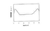
その後、図1(2)に示すように、半導体基板1の上部に、MOSトランジスタ11を覆う状態で窒化シリコン膜13を形成する。この窒化シリコン膜13は、深さ方向に窒素濃度が分布を有して形成されることとする。ただしこの濃度分布は、図2の深さ方向における窒素濃度の分布に示すように、50μm程度の膜厚の窒化シリコン膜における両側の界面層における窒素濃度が中央部分の窒素濃度よりも高いこととする。 Thereafter, as shown in FIG. 1B, a
また、両側界面層における窒素濃度は、高いほど好ましく、さらに好ましくは化学量論的組成であるSi3N4よりも窒素濃度が高いこととする。Further, the higher the nitrogen concentration in the both-side interface layer, the more preferable it is, and it is more preferable that the nitrogen concentration is higher than Si3 N4 which is the stoichiometric composition.
またこれらの界面層に狭持された中央部分の窒素濃度は、窒化シリコン膜13の成膜プロセスにおける熱負荷が、下地に影響を与えることのない程度に成膜時間を短く抑えられる範囲で高いことが好ましい。さらに中央部分の窒素濃度は、窒化シリコン膜13の成膜プロセスにおいて用いられるアンモニアガス(NH3)に由来するパーティクルの発生が、窒化シリコン膜13の膜質の低下を妨げない程度に抑えられる範囲で高いことが好ましい。また、この窒化シリコン膜13は、酸素濃度が十分に低いこととし、酸素の濃度は1×10²⁰個/cm3よりも低いこととする。Further, the nitrogen concentration in the central portion sandwiched between these interface layers is high in a range in which the film formation time can be kept short enough that the thermal load in the film formation process of the
このような窒素濃度の分布を有する窒化シリコン膜13は、窒素含有ガスの供給量を調整した以下の成膜方法によって形成される。尚ここでは、3種類の成膜方法を具体的に説明する。 The
第1に、熱CVD法によって上述した窒素の濃度分布を有する窒化シリコン膜13を形成する場合には、次のように行う。 First, when the
すなわち、熱CVD法による窒化シリコン膜13の成膜は、シリコンを含有する反応ガスと窒素を含有する反応ガスとを、成膜雰囲気内に供給して行われる。シリコンを含有する反応ガスとしては、シラン(SiH4)、ジシラン(Si2H6)、ジクロロジシラン(SiH2Cl2)、ヘキサクロロジシラン(Si2Cl6)などのシラン系ガスが用いられる。また、窒素を含有する反応ガスとしてはアンモニアガス(NH3)が用いられる。That is, the formation of the
そして、特に本実施形態における窒化シリコン膜13の熱CVD法による成膜においては、成膜の1stステップでは、窒素を含有する反応ガスであるアンモニアガス(NH3)の流量を、シリコンを含有する反応ガスであるシラン系ガスの流量よりも充分に大きく設定した成膜を行う。続いて2ndステップでは、1stステップよりもアンモニアガス(NH3)の流量を低下させて通常の流量比での成膜を行う。その後3rdステップでは、2ndステップよりもアンモニアガス(NH3)の流量を上昇させ、1stステップと同様にアンモニアガス(NH3)の流量をシラン系ガスの流量よりも充分に大きく設定した成膜を行う。Particularly in the film formation of the
以上のようなアンモニアガス(NH3)の流量比を変化させた3ステップでの熱CVD成膜により、図2のような窒素濃度の分布を有する窒化シリコン膜13を得る。A
第2に、原子層蒸着法(Atomic Layer Deposition:ALD法)によって上述した窒素濃度の分布を有する窒化シリコン膜13を形成する場合には、次のように行う。 Second, when the
すなわち、原子層蒸着法による窒化シリコン膜13の成膜は、シリコンを含有する反応ガスを供給することで処理表面にSi含有反応物を化学的に吸着させる工程と、窒素を含有する反応ガスを供給することで処理表面に窒素含有反応物を化学的に吸着させる工程との繰り返しによって行われる。 That is, the formation of the
シリコンを含有する反応ガスとしては、上述したシラン系ガスの他、テトラクロロシラン(SiCl4)、テトラキスジメチルアミノシラン(Si[N(CH3)2]4)、テトラキスジエチルアミノシラン(Si[N(C2H5)2]4)、テトラキス1メトキシ2メチル2プロポキシシラン(Si[OC(CH3)2CH2OCH3]4)、トリスジメチルアミノシラン(HSi[N(CH3)2]3)、トリスジエチルアミノシラン(HSi[N(C2H5)2]3)などが用いられる。また、窒素を含有する反応ガスとしてはアンモニアガス(NH3)が用いられる。これらの反応ガスは、アルゴン(Ar)などのキャリアガスと共に所定の流量比で供給される。As the reaction gas containing silicon, other aforementioned silane-based gas, tetrachlorosilane (SiCl4), tetrakis (dimethylamino) silane(Si [N (CH 3) 2] 4), tetrakis (diethylamino) silane (Si [N (C2 H5 )2 ]4 ),
そして、特に本実施形態における窒化シリコン膜13の原子層蒸着法による成膜においては、成膜の1stステップでは、キャリアガスに対するアンモニアガス(NH3)の流量比を充分に大きく設定して、上記工程を繰り返し行う。続いて2ndステップでは、1stステップよりもアンモニアガス(NH3)の流量比を低下させた通常の流量比として上記工程を繰り返し行う。その後3rdステップでは、2ndステップよりもキャリアガスに対するアンモニアガス(NH3)の流量比を上昇させ、1stステップと同様に上記工程を繰り返し行う。In particular, in the film formation of the
以上のようなアンモニアガス(NH3)の流量比を変化させた3ステップでの原子層蒸着法により、図2のような窒素濃度の分布を有する窒化シリコン膜13を得る。The
第3に、プラズマ窒化処理を用いて上述した窒素濃度の分布を有する窒化シリコン膜13を形成する場合には、次のように行う。 Third, when the
すなわち、プラズマ窒化処理を用いた窒化シリコン膜13の成膜は、シリコン膜の成膜処理と、成膜したシリコン膜のプラズマ窒化処理との繰り返しによって行われる。シリコン膜の成膜処理は、上述したシラン系ガスを用いたCVD法によって行われる。また、プラズマ窒化処理は、窒素含有ガスのプラズマ雰囲気にシリコン膜を晒すことによって行われる。 That is, the film formation of the
このような成膜方法においても、繰り返し工程中のプラズマ窒化処理における窒素含有ガスの流量比を3ステップ変化させることにより、図2のような窒素濃度の分布を有する窒化シリコン膜13を得る。 Also in such a film forming method, the
また、このような窒素濃度の分布を有する窒化シリコン膜13の成膜は、上述した3つの成膜方法以外の方法で行われても良く、窒素イオン注入や、窒素プラズマドーピングを用いた手法で行っても良い。窒素イオン注入を行う場合には、予め所定膜厚に形成したシリコン膜に対して、両側の界面層に相当する深さにおいて窒素濃度が高くなるように加速電圧を調整した窒素イオン注入を行う。窒素プラズマドーピングを行う場合には、上述した窒素プラズマ処理を用いた方法において、窒素プラズマ処理を窒素プラズマドーピングに置き換えた成膜を行う。 In addition, the
以上説明した何れかの手法によって、上述した窒素濃度の分布を有する窒化シリコン膜13を形成した後には、図1(3)に示すように、窒化シリコン膜13上に層間絶縁膜15を形成する。ここでは、例えばCVD法によって酸化シリコンからなる層間絶縁膜15を形成することとする。この層間絶縁膜15の成膜は低温プロセスにて行うことが好ましい。そして、この層間絶縁膜15を形成した後には、層間絶縁膜15の改質のためのアニール処理を行う。このアニール処理は、600℃以下の低温プロセスで行われることとする。 After the
その後、ここでの図示は省略したが、窒化シリコン膜13をストッパに用いて層間絶縁膜15をパターンエッチングし、MOSトランジスタ11のソース/ドレイン領域9に達する接続孔を形成する。 After that, although not shown here, the
以上により、両側の界面層における窒素濃度が中央部分の窒素濃度よりも十分に高い窒化シリコン膜13によってMOSトランジスタ11が覆われた半導体装置が得られる。 As described above, a semiconductor device in which the
上述した構成の半導体装置およびその製造方法では、窒化シリコン膜13の特にMOSトランジスタ11側に接する界面層の窒素濃度が十分高いため、窒化シリコン膜13に高い引っ張り応力が生じる。また、両側の界面層の窒素濃度は、例えば化学量論的組成よりも高いため、これらの界面側から酸素が浸入した場合であっても、窒化シリコン膜13内の窒素濃度をある程度に高く保つことができる。具体的には、本実施形態においては、窒化シリコン膜13上に低温プロセスで酸化シリコンからなる層間絶縁膜15を形成しているため、この層間絶縁膜15は水分が多く含まれたものになる。そして、層間絶縁膜15を形成した後には、その膜質改善のためのアニール処理を行うため、このアニール処理においては、層間絶縁膜15から脱離した水分や窒化シリコン膜13の成膜前に半導体基板1側に付着していた水分が窒化シリコン膜13内に侵入し易い。しかしながら、上述したように界面層の窒素濃度が十分に(化学的量論組成よりも)高いため、水分が浸入して窒化シリコン膜13が酸化された場合であっても、窒化シリコン膜13内における窒素濃度を高く保つことが可能なのである。したがって、窒化シリコン膜13における高く安定した引っ張り応力を維持することができ、特にnMOSトランジスタにおける特性の向上を図ることができる。 In the semiconductor device having the above-described configuration and the manufacturing method thereof, a high tensile stress is generated in the
しかも、この窒化シリコン膜13においては、これらの界面層に挟まれた中央部の窒素濃度が低く設定されているため、全層にわたって窒素濃度が高い窒化シリコン膜と比較して、より短時間で成膜することが可能になり、生産性の向上が図られる。またこれと共に成膜に要する熱負荷が抑えられるため、既に形成されている下地部材への熱負荷の影響を小さく抑えることが可能であり、活性層の不活性化やシリサイド層の高抵抗化を抑えることができる。 In addition, in the
また、窒化シリコン膜13における中央部の窒素濃度が低く設定されていることにより、窒化シリコン膜13を形成する際の窒素含有ガスの全体的な供給量が抑えられ、パーティクル発生の少ない環境で成膜することが可能になり、全体として膜質の良好な窒化シリコン膜13を得ることができる。 In addition, since the nitrogen concentration in the central portion of the
以上の結果、熱負荷をより小さく抑えて下地への影響なく成膜可能であると共に、パーティクルの発生を抑えた環境で成膜されたことにより膜質が良好でかつ十分に引っ張り応力を維持可能な窒化シリコン膜によって、MOSトランジスタを覆うことが可能となる。この結果、トランジスタ特性の向上を図ることが可能になる。 As a result of the above, it is possible to form a film without affecting the substrate by reducing the thermal load, and the film is formed in an environment where the generation of particles is suppressed, so that the film quality is good and sufficient tensile stress can be maintained. The silicon nitride film can cover the MOS transistor. As a result, transistor characteristics can be improved.
1…半導体基板、11…MOSトランジスタ(電界効果トランジスタ)、13…窒化シリコン膜 DESCRIPTION OF
Claims (6)
Translated fromJapanese前記窒化シリコン膜は、当該窒化シリコン膜の上面側及び下面側の界面層における窒素濃度が当該窒化シリコン膜の上面側及び下面側の界面層に挟持された部分の窒素濃度よりも高く、かつ、引っ張り応力を有する
ことを特徴とする半導体装置。In a semiconductor device provided with a silicon nitride film in a state of covering a field effect transistor formed on the surface side of a semiconductor substrate,
In the silicon nitride film, the nitrogen concentration in the interface layer on the upper surface side and the lower surface side of the silicon nitride film is higher than the nitrogen concentration in the portion sandwiched between the interface layers on the upper surface side and the lower surface side of the silicon nitride film, and A semiconductor device characterized by having a tensile stress.
前記窒化シリコン膜の上面側及び下面側の界面層における窒素濃度は、化学量論的組成よりも高い
ことを特徴とする半導体装置。The semiconductor device according to claim 1,
The semiconductor device, wherein a nitrogen concentration inan interface layeron anupper surface side and a lower surface side of the silicon nitride film is higher than a stoichiometric composition.
前記窒化シリコン膜を形成する工程では、当該窒化シリコン膜の上面側及び下面側の界面層における窒素濃度が、当該窒化シリコン膜の上面側及び下面側の界面層に挟持された部分の窒素濃度よりも高くなるように窒素含有ガスの供給量を調整した成膜が行われ、前記窒化シリコン膜が引っ張り応力を有する
ことを特徴とする半導体装置の製造方法。A method of manufacturing a semiconductor device, comprising: a step of forming a field effect transistor on a surface side of a semiconductor substrate; and a step of forming a silicon nitride film so as to cover the field effect transistor,
In the step of forming the silicon nitride film, the nitrogen concentration in the interface layer on the upper surface side and the lower surface side of the silicon nitride film is greater than the nitrogen concentration in the portion sandwiched between the interface layers on the upper surface side and the lower surface side of the silicon nitride film. The method for manufacturing a semiconductor device is characterized in that film formation is performed by adjusting a supply amount of a nitrogen-containing gas so as to be higher, and the silicon nitride film has tensile stress.
前記窒化シリコン膜を形成する工程は熱CVD法によって行われる
ことを特徴とする半導体装置の製造方法。In the manufacturing method of the semiconductor device according to claim 3,
The method of manufacturing a semiconductor device, wherein the step of forming the silicon nitride film is performed by a thermal CVD method.
前記窒化シリコン膜を形成する工程は原子層蒸着法によって行われる
ことを特徴とする半導体装置の製造方法。In the manufacturing method of the semiconductor device according to claim 3,
The method of manufacturing a semiconductor device, wherein the step of forming the silicon nitride film is performed by an atomic layer deposition method.
前記窒化シリコン膜を形成する工程は、シリコン膜の成膜処理と当該シリコン膜のプラズマ窒化処理との繰り返しによって行われる
ことを特徴とする半導体装置の製造方法。In the manufacturing method of the semiconductor device according to claim 3,
The method of manufacturing a semiconductor device, wherein the step of forming the silicon nitride film is performed by repeating a silicon film forming process and a plasma nitriding process of the silicon film.
Priority Applications (1)
| Application Number | Priority Date | Filing Date | Title |
|---|---|---|---|
| JP2004198990AJP4876375B2 (en) | 2004-07-06 | 2004-07-06 | Semiconductor device and manufacturing method thereof |
Applications Claiming Priority (1)
| Application Number | Priority Date | Filing Date | Title |
|---|---|---|---|
| JP2004198990AJP4876375B2 (en) | 2004-07-06 | 2004-07-06 | Semiconductor device and manufacturing method thereof |
Publications (2)
| Publication Number | Publication Date |
|---|---|
| JP2006024609A JP2006024609A (en) | 2006-01-26 |
| JP4876375B2true JP4876375B2 (en) | 2012-02-15 |
Family
ID=35797696
Family Applications (1)
| Application Number | Title | Priority Date | Filing Date |
|---|---|---|---|
| JP2004198990AExpired - Fee RelatedJP4876375B2 (en) | 2004-07-06 | 2004-07-06 | Semiconductor device and manufacturing method thereof |
Country Status (1)
| Country | Link |
|---|---|
| JP (1) | JP4876375B2 (en) |
Families Citing this family (3)
| Publication number | Priority date | Publication date | Assignee | Title |
|---|---|---|---|---|
| JP5182703B2 (en)* | 2006-06-08 | 2013-04-17 | 日本電気株式会社 | Semiconductor device |
| KR100807597B1 (en) | 2006-09-28 | 2008-02-28 | 주식회사 하이닉스반도체 | Manufacturing Method of Semiconductor Device |
| JP2008218661A (en)* | 2007-03-02 | 2008-09-18 | Fujitsu Ltd | Field effect semiconductor device and method for manufacturing the same |
Family Cites Families (6)
| Publication number | Priority date | Publication date | Assignee | Title |
|---|---|---|---|---|
| DE69333722T2 (en)* | 1993-05-31 | 2005-12-08 | Stmicroelectronics S.R.L., Agrate Brianza | Method for improving the adhesion between dielectric layers, at their interface, in the manufacture of semiconductor devices |
| JP2000340561A (en)* | 1999-05-25 | 2000-12-08 | Tokyo Electron Ltd | Method for forming film |
| JP2003086708A (en)* | 2000-12-08 | 2003-03-20 | Hitachi Ltd | Semiconductor device and manufacturing method thereof |
| JP2002198368A (en)* | 2000-12-26 | 2002-07-12 | Nec Corp | Method for manufacturing semiconductor device |
| JP2002252229A (en)* | 2001-02-16 | 2002-09-06 | Applied Materials Inc | Method and apparatus for forming nitride film |
| US6509282B1 (en)* | 2001-11-26 | 2003-01-21 | Advanced Micro Devices, Inc. | Silicon-starved PECVD method for metal gate electrode dielectric spacer |
- 2004
- 2004-07-06JPJP2004198990Apatent/JP4876375B2/ennot_activeExpired - Fee Related
Also Published As
| Publication number | Publication date |
|---|---|
| JP2006024609A (en) | 2006-01-26 |
Similar Documents
| Publication | Publication Date | Title |
|---|---|---|
| KR100852585B1 (en) | Semiconductor device and method for fabricating the same | |
| KR100943113B1 (en) | Method for silicon nitride chemical vapor deposition | |
| JP4906270B2 (en) | New materials for contact and etch layers that improve device performance | |
| US7528424B2 (en) | Integrated circuitry | |
| US20070072381A1 (en) | Method for fabricating a semiconductor device including the use of a compound containing silicon and nitrogen to form an insulation film of SiN, SiCN or SiOCN | |
| KR20110095456A (en) | Transistors and manufacturing methods thereof | |
| KR20130047594A (en) | Method of forming silicon oxide film | |
| CN103069552A (en) | Mos transistors including sion gate dielectric with enhanced nitrogen concentration at its sidewalls | |
| WO2013074169A1 (en) | Germanium oxide free atomic layer deposition of silicon oxide and high-k gate dielectric on germanium containing channel for cmos devices | |
| JP4876375B2 (en) | Semiconductor device and manufacturing method thereof | |
| JP2008010881A (en) | Manufacturing method of semiconductor device | |
| JP2740722B2 (en) | Semiconductor device and manufacturing method thereof | |
| JP2002222941A (en) | MIS type semiconductor device and method of manufacturing the same | |
| JP3753994B2 (en) | Manufacturing method of semiconductor device | |
| JP7448924B2 (en) | semiconductor device | |
| KR100935719B1 (en) | Dual gate formation method of semiconductor device | |
| US7358198B2 (en) | Semiconductor device and method for fabricating same | |
| US20110008938A1 (en) | Thin film and method for manufacturing semiconductor device using the thin film | |
| JPH10125617A (en) | Method for manufacturing semiconductor device | |
| JP2006054382A (en) | Metallic silicate film, manufacturing method thereof, semiconductor device, and manufacturing method thereof | |
| JP2007157866A (en) | Film-forming method and semiconductor device manufacturing method | |
| JP2008041825A (en) | Method of manufacturing semiconductor device | |
| KR100445058B1 (en) | Method for forming gate oxide in semiconductor device | |
| CN116536645A (en) | Semiconductor substrate and method for manufacturing the same | |
| KR20200073452A (en) | A Method of Silicon Insulating Film Deposition at Low Temperature |
Legal Events
| Date | Code | Title | Description |
|---|---|---|---|
| A621 | Written request for application examination | Free format text:JAPANESE INTERMEDIATE CODE: A621 Effective date:20070405 | |
| A977 | Report on retrieval | Free format text:JAPANESE INTERMEDIATE CODE: A971007 Effective date:20090108 | |
| RD02 | Notification of acceptance of power of attorney | Free format text:JAPANESE INTERMEDIATE CODE: A7422 Effective date:20091009 | |
| RD04 | Notification of resignation of power of attorney | Free format text:JAPANESE INTERMEDIATE CODE: A7424 Effective date:20091029 | |
| A131 | Notification of reasons for refusal | Free format text:JAPANESE INTERMEDIATE CODE: A131 Effective date:20110215 | |
| A521 | Request for written amendment filed | Free format text:JAPANESE INTERMEDIATE CODE: A523 Effective date:20110328 | |
| A131 | Notification of reasons for refusal | Free format text:JAPANESE INTERMEDIATE CODE: A131 Effective date:20110802 | |
| A521 | Request for written amendment filed | Free format text:JAPANESE INTERMEDIATE CODE: A523 Effective date:20110926 | |
| TRDD | Decision of grant or rejection written | ||
| A01 | Written decision to grant a patent or to grant a registration (utility model) | Free format text:JAPANESE INTERMEDIATE CODE: A01 Effective date:20111101 | |
| A01 | Written decision to grant a patent or to grant a registration (utility model) | Free format text:JAPANESE INTERMEDIATE CODE: A01 | |
| A61 | First payment of annual fees (during grant procedure) | Free format text:JAPANESE INTERMEDIATE CODE: A61 Effective date:20111114 | |
| FPAY | Renewal fee payment (event date is renewal date of database) | Free format text:PAYMENT UNTIL: 20141209 Year of fee payment:3 | |
| R250 | Receipt of annual fees | Free format text:JAPANESE INTERMEDIATE CODE: R250 | |
| LAPS | Cancellation because of no payment of annual fees |