JP4874465B2 - Eddy current loss measurement sensor - Google Patents
Eddy current loss measurement sensorDownload PDFInfo
- Publication number
- JP4874465B2 JP4874465B2JP2001028187AJP2001028187AJP4874465B2JP 4874465 B2JP4874465 B2JP 4874465B2JP 2001028187 AJP2001028187 AJP 2001028187AJP 2001028187 AJP2001028187 AJP 2001028187AJP 4874465 B2JP4874465 B2JP 4874465B2
- Authority
- JP
- Japan
- Prior art keywords
- eddy current
- film thickness
- conductive film
- measurement
- coil
- Prior art date
- Legal status (The legal status is an assumption and is not a legal conclusion. Google has not performed a legal analysis and makes no representation as to the accuracy of the status listed.)
- Expired - Fee Related
Links
Images


Classifications
- G—PHYSICS
- G01—MEASURING; TESTING
- G01B—MEASURING LENGTH, THICKNESS OR SIMILAR LINEAR DIMENSIONS; MEASURING ANGLES; MEASURING AREAS; MEASURING IRREGULARITIES OF SURFACES OR CONTOURS
- G01B11/00—Measuring arrangements characterised by the use of optical techniques
- G01B11/02—Measuring arrangements characterised by the use of optical techniques for measuring length, width or thickness
- G01B11/06—Measuring arrangements characterised by the use of optical techniques for measuring length, width or thickness for measuring thickness ; e.g. of sheet material
- G01B11/0608—Height gauges
- G—PHYSICS
- G01—MEASURING; TESTING
- G01B—MEASURING LENGTH, THICKNESS OR SIMILAR LINEAR DIMENSIONS; MEASURING ANGLES; MEASURING AREAS; MEASURING IRREGULARITIES OF SURFACES OR CONTOURS
- G01B7/00—Measuring arrangements characterised by the use of electric or magnetic techniques
- G01B7/02—Measuring arrangements characterised by the use of electric or magnetic techniques for measuring length, width or thickness
- G01B7/06—Measuring arrangements characterised by the use of electric or magnetic techniques for measuring length, width or thickness for measuring thickness
- G01B7/10—Measuring arrangements characterised by the use of electric or magnetic techniques for measuring length, width or thickness for measuring thickness using magnetic means, e.g. by measuring change of reluctance
- G01B7/105—Measuring arrangements characterised by the use of electric or magnetic techniques for measuring length, width or thickness for measuring thickness using magnetic means, e.g. by measuring change of reluctance for measuring thickness of coating
Landscapes
- Physics & Mathematics (AREA)
- General Physics & Mathematics (AREA)
- Measurement Of Length, Angles, Or The Like Using Electric Or Magnetic Means (AREA)
- Transmission And Conversion Of Sensor Element Output (AREA)
- Tests Of Electronic Circuits (AREA)
Description
Translated fromJapanese【0001】
【発明の属する技術分野】
本発明は、膜厚の測定装置に関し、特に、半導体集積回路装置の製造工程において、高周波磁界を励磁してウェーハ表面の導電性膜に励起される渦電流による渦電流損失を測定する渦電流測定センサ、並びに、測定された渦電流損失に基づいて上記導電性膜の膜厚を非接触に測定する測定装置、膜厚測定方法およびコンピュータ読取り可能な記録媒体を対象とする。
【0002】
【従来の技術】
渦電流を用いて導電性膜の膜厚を測定する方法は、非接触かつ非破壊の膜厚測定技術として有効である。
【0003】
渦電流を用いた膜厚測定方法において、磁場を発生させるコイル(センサ)と導電性膜との距離は、導電性膜内における渦電流損失量に強く影響する。このため、センサと導電性膜との間の距離を高い精度で制御することが重要となる。
【0004】
図23は、渦電流損失量をセンサのインダクタンスおよび抵抗の変化として測定した一実験例のデータである。同図からも、センサと導電性膜との間の距離に応じて、センサのインダクタンスおよび抵抗が変化することがわかる。
【0005】
このような距離依存性による測定誤差を減少させ、測定精度の向上を図るために、次のような技術が提案されている。
【0006】
例えば、第1の方法として、図23に示すように、センサおよび導電性膜間の距離と測定値との相関関係を予め求めておき、センサと導電性膜との距離を変えて複数点の測定を行った上で、各測定点ごとに上記相関関係を用いて補正する方法がある。
【0007】
また、第2の方法として、図24に示すように、測定対象とする導電性膜101の表裏に、渦電流を励起するコイル103a,103bを対向設置し、これらのコイル103a,103bを直列に接続して得られるインダクタンスのQをインピーダンスアナライザ104により測定する方法がある。
【0008】
【発明が解決しようとする課題】
しかしながら、上述した第2の測定方法によれば、装置の構成が複雑で大掛かりなものになるという欠点がある。
【0009】
また、距離を変えて複数点測定する第1の方法では、センサまたはステージを測定回数分だけ動作させなければならない上、測定点毎にデータ処理を行わなければならないので、膨大な測定時間が必要となる。従って、大量生産ラインにおいて求められる高速測定または膜厚形成工程におけるリアルタイム測定には不向きであるため、実用性に乏しい、という問題があった。
【0010】
一方、局所的な膜厚測定を可能にして測定精度を向上させるため、コイルで発生させた磁場を一点に集中させる試みは、コイル径を小さくして分解能を上げる方法の他、図25に示すように、コイル108内にフェライトまたは磁性材料のコア110を挿入する方法しか行われていなかった。
【0011】
金属導線の変位を測定するセンサとして、導線上に磁場を集中させるセンサが提案されている。その一例を図26を参照しながら説明する。
【0012】
図26に示す変位センサは、同図(a)に示すように、フェライトコア111に巻き着けられた受信コイル112と、受信コイル112の外側に巻き着けられた高周波励磁コイル113と、フェライトコア111、コイル112,113を覆うように設けられた銅製でなる上開の外側遮蔽板114を備える。
【0013】
高周波励磁コイル113は、高周波電流を受けて磁場を発生させ、測定対象である金属導線Cに渦電流を励起する。受信コイル112は、金属導線Cで発生した渦電流により磁束密度が低減した磁場を受信する。
【0014】
外側遮蔽板114は、対向配置される半円筒部114aと114bにより構成され、図26(b)に代表的に示すように各半円筒部は半円状の底板半部114c,114dを有する。この左右の両半円筒部114aと114bを微小な細隙を介して対向配置し、図26(c)の底面図に示すように、各底板半部114c,114dの間に直径線方向に絶縁スリット115を形成する。このように、外側遮蔽板114は、絶縁スリット115により左右に分割され相互に絶縁された各半部で構成される。本例では線状の絶縁スリットを示したが、十字状の絶縁スリットを形成しても良い。
【0015】
高周波励磁コイル113に高周波励磁電流を流すと高周波磁界が発生し、外側遮蔽板114の左右の各底板半部114c,114dに渦電流が誘導される。この渦電流は磁界を妨げる方向に生ずるので、励磁コイル113による磁界と各底板半部114c,114dの渦電流による磁界との合成磁界は、各底板半部114c,114dにおいて磁束密度が小さく、絶縁スリット115において磁束密度が大きくなる。このため、センサヘッドには図26(d)に示すように、絶縁スリット部S0において磁束密度が最大値Bmaxとなる不均一な高周波磁界が構成される。従って、図26(a)に示すように、銅線等の金属導線Cの上方にセンサヘッドを配置すると、外側遮蔽板114の絶縁スリット115の直下に導線Cがあれば、導線Cが占める空間の電束密度が最も大きく、また導線Cの渦電流に誘起された交流磁界に対して外側遮蔽板114の遮蔽効果が最も弱くなり、この時センサヘッドの受信コイル112のインピーダンスに対する導線Cの影響が最も大きくなる。
【0016】
このように、線状または十字状のスリットにより、縦長の領域へ磁束を出す構造は、金属導線のような細長い物体の変位を調べるために有効ではあるが、局所的な膜厚測定に用いる場合は、スポットとしての磁場を形成する必要があるため、不十分であった。
【0017】
本発明は上記事情に鑑みてなされたものであり、その目的は、局所的な膜厚測定を可能とする渦電流損失測定センサを提供することにある。
【0018】
【課題を解決するための手段】
本発明は、以下の手段により上記課題の解決を図る。
【0019】
即ち、本発明の第1の態様によれば、
高周波電流を受けて高周波磁界を励磁して測定対象である導電性膜に渦電流を励起するとともに、前記渦電流により発生する磁界と前記高周波磁界との合成磁界を受信する円筒形状の励起受信一体型コイルと、
第1の透磁性材料で形成され、前記励起受信一体型コイル内に挿設されてコアをなす円柱形状の第1の透磁性部材と、
第2の透磁性材料で形成され、前記第1の透磁性部材および前記励起受信一体型コイルを包むように設けられ、前記導電性膜との対向面において前記励起受信一体型コイルの一部の領域のみが露出するように前記第1の透磁性部材を周回する円環状の開口が形成された第2の透磁性部材と、
を備え、
前記第1の透磁性部材の前記導電性膜との対向面と、前記第2の透磁性部材の前記導電性膜との対向面とは同一平面に配置される、
非接触型の渦電流損失測定センサが提供される。
【0021】
また、本発明の第2の態様によれば、
高周波電流を受けて高周波磁界を励磁して測定対象である導電性膜に渦電流を励起する円筒形状の渦電流励起コイルと、
前記渦電流励起コイル内で前記渦電流励起コイルにより周回されるように設けられ、前記渦電流により発生する磁界と前記高周波磁界との合成磁界を受信する円筒形状の受信コイルと、
第1の透磁性材料で形成され、前記受信コイル内に挿設されてコアをなす円柱形状の第1の透磁性部材と、
第2の透磁性材料で形成され、前記第1の透磁性部材、前記受信コイルおよび前記渦電流励起コイルを包むように設けられ、前記導電性膜との対向面において前記受信コイルの一部の領域のみが露出するように前記第1の透磁性部材を周回する円環状の開口が形成された第2の透磁性部材と、
を備え、
前記第1の透磁性部材の前記導電性膜との対向面と、前記第2の透磁性部材の前記導電性膜との対向面とは同一平面に配置される、
非接触型の渦電流損失測定センサが提供される。
【0087】
【発明の実施の形態】
以下、本発明の実施の形態のいくつかについて図面を参照しながら説明する。なお、以下の各図において同一の部分には同一の参照番号を付してその説明を適宜省略する。
【0088】
(1)渦電流損失測定センサの実施形態
まず、本発明にかかる渦電流損失測定センサの実施の形態のいくつかについて説明する。
【0089】
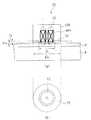
(a)渦電流損失測定センサの第1の実施形態
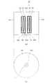
図1(a)は、本発明にかかる渦電流損失測定センサの第1の実施の形態を示す略示断面図であり、また、同図(b)は、その底面図である。
【0090】
図1(a)に示すように、本実施形態の渦電流損失測定センサ10は、円筒形状のコイル12と、コイル12の内部に挿設されるフェライトコア14a(第1の透磁性部材)と、コイル12およびフェライトコア14aを包むように設けられたフェライト14b〜14d(第2の透磁性部材)とを備えている。
【0091】
コイル12は、図示しない高周波電源から高周波電流を受けて磁場を形成するとともに、測定対象物である導電性膜9に励起される渦電流で生成される磁場を受信する、励起受信一体型コイルとなっている。
【0092】
中心軸をなすフェライトコア14aと周辺のフェライト14b〜14dはいずれも比較的高い比透磁率、例えば400を有する。
【0093】
本実施形態の渦電流損失測定センサの特徴は、フェライト14のうち、導電性膜9との対向面である底面に位置するフェライト14b中に開口16が形成されている点にある。開口16は、図1(b)にも示すように、フェライト14bにおいてフェライトコア14aの周辺領域で円環の窪みをなすように形成され、その底面においてコイル12の底面が露出する形状となっている。また、開口16の表面とフェライト14a、14bの表面領域のうち開口16の近傍領域には、フェライト14a、14bの材料よりもさらに透磁率が高い高透磁率材料によりメッキが施されている。これにより、局所的な領域にのみ磁束MF1を集中して浸み出すことが可能になる。
【0094】
図1に示す渦電流損失測定センサ10の動作は次のとおりである。
【0095】
コイル12に高周波電流を供給すると、コイル12により発生した磁束線MF1は、フェライトコア14aの中心軸を通って開口16に達し、開口16内からのみ外部に漏れ出し、コイル12の下方で一頂点をなす急峻な放物線を描いてフェライト14b内へ戻り、側面部のフェライト14c、頂部フェライト14dを経由してフェライトコア14aの中心軸に再び戻る、という磁路を形成する。従って、渦電流損失測定センサ20の側面方向への磁場分布が非常に小さく抑えられることに加え、底部のフェライト14bの中央領域に円環状の開口16が形成され、さらに開口16の外側周面と開口16を周回するフェライト14bの表面領域に磁性材料メッキが施されているために、磁束は開口16からのみ外部へ漏れ出す。
【0096】
従って、開口16から漏れ出す磁束線が描く放物線が導電性膜9内に到達するように、渦電流損失測定センサ10を導電性膜9に近接して配置すれば、コイル12の下方領域でのみ渦電流が局所的に励起される。この渦電流により発生した磁界とコイル12から発生した磁界との合成磁界を受けたコイル12のインピーダンス、高周波電流の電流値または高周波電流の位相の変化を測定することにより、局所的に渦電流損失量を測定することができる。
【0097】
図2は、渦電流損失測定センサ10に高周波電流を供給した場合に、導電性膜9の表面に分布する磁束密度をシミュレーションにより求めたグラフである。同図中、実線に示すグラフが渦電流損失測定センサ10を用いた場合のシミュレーション結果であり、また、点線に示すグラフが従来の技術による渦電流損失測定センサの一例を用いた場合のシミュレーション結果である。図2から明らかなように、本実施形態によれば、センサ中心から半径(R)約0.3mmの領域内で磁束密度が集中して分布しており、従来の技術と比較して極めて微小な領域にのみ分布していることがわかる。
【0098】
このように、本実施形態の渦電流損失測定センサ10によれば、開口16からのみ磁束が外部へ漏れ出すので、開口16が導電性膜9に対向するように、かつ、十分な磁束線が導電性膜9内を通過する距離、例えば0.3mmだけ引き離して配置することにより、導電性膜9内の極めて微小な領域でのみ渦電流を発生させることができる。この渦電流の影響により合成磁界が変化するので、渦電流損失測定センサ10のインピーダンス、高周波電流の電流値または高周波電流の位相の変化を測定することにより、渦電流損失量を高精度に測定することができる。
【0099】
(b)渦電流損失測定センサの第2の実施形態
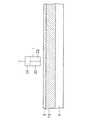
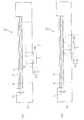
次に、本発明にかかる渦電流損失測定センサの第2の実施の形態について図3を参照しながら説明する。
【0100】
図3(a)は、本実施形態の渦電流損失測定センサ20を示す略示断面図であり、また、同図(b)は、その底面図である。図1との対比において明らかなように、本実施形態の特徴は、センサ内のコイルとして、渦電流励起コイル24と受信コイル22とを有する点にある。その他の構成は、上述した渦電流損失測定センサ10と略同一である。また、本実施形態の渦電流損失測定センサ20の動作も、前述した第1の実施形態と実質的に同一である。
【0101】
このように、本実施形態によれば、渦電流励起用と渦電流損失受信用にそれぞれ機能が分化された2つのコイルを用いるので、より優れた分解能を有する渦電流損失測定センサが提供される。
【0102】
上述した2つの実施形態において、フェライト14b〜14dは、開口16を除いてフェライトコア14aおよび、コイル12またはコイル22,24を覆う形状で構成したが、本発明にかかる渦電流損失測定センサは、開口16から局所的に磁束が外部に漏れ出す形状であれば、これらの形状に限るものではない。例えば、フェライトコア14aとフェライト14bのコイル下方の領域の表面にのみ磁性材膜をつけた形態でも良く、また、フェライト14cの外周面にのみ磁性材膜をつけることとしても良い。また、第1および第2の透磁性材料としてフェライト材を用いたが、これに限ることなく、透磁率μが高いものであれば他の透磁性材料を用いても良い。また、第1および第2の透磁性部材においても、全部について均一の透磁率を有する必要はなく、磁界がセンサ周辺に漏れることを防止し、導電性膜9の局所的な領域にのみ漏れ磁束を集中させることができるものであれば、その一部または全部をさらに透磁率の高い透磁性材料に置換できるのは勿論である。
【0103】
(2)膜厚測定装置の実施形態
次に、本発明にかかる膜厚測定装置の実施の形態のいくつかについて図面を参照しながら説明する。
【0104】
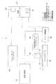
(a)膜厚測定装置の第1の実施形態
図4は、本発明にかかる膜厚測定装置の第1の実施の形態の概略構成を示すブロック図である。同図に示すように、本実施形態の膜厚測定装置1は、X−Y−Zステージ36と、前述した渦電流損失測定センサ20と、Zステージ34と、ステージ駆動部38と、光学式変位センサ32と、光学式変位センサコントローラ46と、高周波電源44と、インピーダンスアナライザ48と、装置全体を制御する制御コンピュータ42と、を備える。
【0105】
X−Y−Zステージ36は、表面に測定対象である導電性膜9(図1参照)が成膜された半導体ウェーハ8を上面に載置し、ステージ駆動部38から制御信号の供給を受けてX−Y−Zの任意の方向に半導体ウェーハ8を移動する。X−Y−Zステージ36は、絶縁材料または導電率が低い材料で形成され、渦電流損失測定センサ20により発生する高周波磁界を受けても渦電流が全く発生しないか、または、測定上無視できるほど微少量の渦電流しか発生しないようになっている。
【0106】
光学式変位センサ32は、光学式変位センサコントローラ46から供給される制御信号により、渦電流損失測定センサ20と導電性膜9との間の距離を測定し、測定値を光学式変位センサコントローラ46を介して制御コンピュータ42に供給する。光学式変位センサ32と光学式変位センサコントローラ46は、本実施形態における距離測定手段を構成する。
【0107】
Zステージ34は、渦電流損失測定センサを釣支するとともに、ステージ駆動部38から制御信号の供給を受けて渦電流損失測定センサをZ方向に移動する。
【0108】
ステージ駆動部38は、制御コンピュータ42から指令信号を受けてX−Y−Zステージ36およびZステージ34に制御信号を供給する。
【0109】
高周波電源44は、制御コンピュータ42の指令信号に基づいて渦電流損失測定センサの渦電流励起コイル24(図3参照)に所望の周波数の高周波電流を供給する。電流の周波数は、本実施形態において約1MHz〜約10MHzである。
【0110】
高周波電流の供給を受けた渦電流励起コイル24は、高周波磁界を形成し、これにより、導電性膜9に局所的に渦電流が発生する。受信コイル22は、導電性膜9の渦電流により発生した磁界とコイル24により発生した磁界との合成磁界を受信する。
【0111】
インピーダンスアナライザ48は、渦電流損失測定センサ20の受信コイル22(図3参照)に接続され、計測用の高周波電流を受信コイル22に供給し、渦電流損失測定センサ20のインピーダンスにおける渦電流損の影響による変化、計測用高周波電流の電流値における渦電流損の影響による変化または計測用高周波電流の位相における渦電流損の影響による変化を測定して測定結果を制御コンピュータ42に供給する。
【0112】
制御コンピュータ42は、膜厚演算部54とメモリ52とを有する。
【0113】
メモリ52には、測定手順のプログラムおよび各種の測定用データテーブルを含むレシピファイルが格納される。
【0114】
測定用データとしては、渦電流損失測定センサと導電性膜9との間の距離DSF,高周波電源44から供給される電流の周波数f,導電性膜9の膜厚t,導電性膜9の抵抗率ρに対する、渦電流損失の影響を受けた渦電流損失測定センサのインピーダンスの変化、インピーダンスアナライザ48の計測用高周波電流の電流値値の変化または計測用高周波電流の電流の位相の変化との関係を示すデータが含まれる。これらのデータは、膜厚tの算出のため、または渦電流損失測定センサと導電性膜9との間の距離DSFの補正のために用いられる。
【0115】
制御コンピュータ42はメモリ52からレシピファイルを読出し、このレシピファイルに含まれる測定プログラムに基づいて測定装置1の上述した各構成要素を制御する。
【0116】
図5および図6は、レシピファイル内に含まれる測定用データテーブルの具体例を示す。図5は、渦電流損失測定センサ20と導電性膜9との間の距離DSFに対する渦電流損失測定センサ20のインダクタンスL(H)の変化と抵抗値R(Ω)の変化を膜厚t(0,0.15,1.0,2.0)μmをパラメータとして表した一例である。また、図6は、渦電流損失測定センサ20と導電性膜9との間の距離DSFに対応して変化する渦電流損失測定センサ20のインダクタンス(H)と抵抗値(Ω)の値を抵抗率ρ(ρ1,ρ2)をパラメータとして表した一例である。両図において、実線に示すグラフはインダクタンスLの変化を示し、点線に示すグラフは抵抗値Rの変化を示す。
【0117】
制御コンピュータ42の膜厚演算部54は、インピーダンスアナライザ48から供給された測定結果をレシピファイル内のデータテーブルと照合することにより導電性膜9の膜厚tを算出する。
【0118】
図4に示す膜厚測定装置1を用いた膜厚測定方法について以下に説明する。
【0119】
本実施形態の膜厚測定装置1は、上述した膜厚測定を半導体製造工程における導電性膜の成膜工程、エッチング工程または研磨工程と並行してパイプライン的に実行することができる。
【0120】
膜厚の測定方法としては、導電性膜9と渦電流損失測定センサ20間の距離を一定に保持しながら測定する第1の測定方法と、導電性膜9と渦電流損失測定センサ20間の距離の測定結果を用いてインピーダンスアナライザ48の測定結果から算出された膜厚tの測定値を補正する第2の測定方法と、膜厚の測定に先立って導電性膜9と渦電流損失測定センサ20間の距離の変化をデータテーブルとして予め取得し、このデータテーブルに基づいてウェーハの反りなどに起因する測定誤差を除去しながら導電性膜9の膜厚を測定する第3の測定方法とがある。
【0121】
第1の測定方法では、光学式変位センサ32の測定結果に基づいてステージ駆動部38によりX−Y−Zステージ36とZステージ34の双方を動作させる処理を含む。また、第2の方法では、Zステージ34は動作させることなく、光学式変位センサ32の測定結果に基づいて膜厚tの測定値を補正する処理を含む。さらに、第3の測定方法では、プレスキャンにより得られた距離測定結果に対して測定範囲における膜厚測定点の変位を近似的に算出する処理を含む。
【0122】
図4に示す膜厚測定装置1においては、第1の測定方法または第2の測定方法のいずれの方法にも適用することができるが、以下では、第1の測定方法に適用した場合について説明する。
【0123】
測定中は、測定の基準となる値(以下、基準値という)を逐次測定し、測定誤差を補正する(第1の補正処理)。これは、成膜工程中、エッチング工程中または研磨工程中に、膜厚測定装置1の周囲の温度が変化したり、インピーダンスアナライザ48自体に揺らぎが発生するなどの原因で、測定値のドリフトが発生することがあるからである。具体的には、導電性膜9の膜厚測定と並行してX−Y−Zステージ36の周辺領域で渦電流損失の影響を常時受けることがない領域で渦電流損失測定センサのインピーダンス、高周波電流の電流値または高周波電流の位相を逐次測定する。例えば図7に示すように、成膜時間tの経過とともに、導電性膜9が成膜されていない領域のインダクタンスが測定開始時t0においてL0t0であり、t1においてにL0t1にまで増加した場合は、(L0t1−L0t0)は測定誤差であると判断できる。そこで、導電性膜9が成膜された領域の測定結果L1t1に対してL0t0だけ減算する補正処理を行う。
【0124】
最初に、高周波電源44が供給する高周波電流の周波数fを設定する。これは、測定対象である導電性膜9を成膜するときの狙いの膜厚t、即ち、設計上の膜厚値を参照し、レシピファイル内の膜厚と分解能との関係を示すデータテーブルに基づいて最適と思われる周波数fを設定する。
【0125】
図8は、導電性膜9の膜厚t(μm)と測定装置の分解能(μm)との関係を周波数fをパラメータとして測定した例を示す。同図のグラフからわかるように、導電性膜9の狙いとする膜厚tが薄いほど、使用する高周波電流の周波数fを高くすることで、装置の分解能を高めることができる。これは、渦電流を励起する磁場の周波数により、渦電流の導電性膜への浸透深度が変化する特徴を利用したものである。
【0126】
このようにして周波数fが設定された高周波電流を渦電流損失測定センサ20に供給し、渦電流励起コイル24から高周波の磁場が発生し、開口部16から漏れだした磁束が導電性膜9内を通過すると、導電性膜9に渦電流が励起され、次記する式1で表される渦電流損失Pが発生する。
【0127】
P=(f2・t)/ρ・・・・・・(1)
ここで、導電性膜9の抵抗率ρは、成膜しようとする導電性膜9の材質から予め与えられる。
【0128】
導電性膜9でこのような渦電流損失Pが発生すると、導電性膜9の膜厚tに応じて受信コイル22のインピーダンス、受信コイル22に流れる計測用の高周波電流の電流値または高周波電流の位相が変化する。
【0129】
図9は、成膜の進行により導電性膜9の膜厚tが変化した時の渦電流損失測定センサのインダクタンスと抵抗値の変化を測定した一例を示す。同図において、実線で示すグラフはインダクタンスLの変化を示し、点線に示すグラフは抵抗値Rの変化を示す。
【0130】
インピーダンスアナライザ48は、図9に示すような変化をモニタして制御コンピュータ42に供給する。制御コンピュータ42の膜厚演算部54は、予め作成されレシピファイルに書き込まれた、膜厚tと膜の抵抗値との関係を示すデータテーブルを参照しながら膜厚tを演算して出力する。
【0131】
膜厚測定装置1は、以上の膜厚測定をウェーハ8の全面にわたって処理する。即ち、X−Y−Zステージ36がレシピファイルに予め設定された手順に従って連続的に移動し、これにより、ウェーハ8の表面が渦電流損失測定センサ20によって走査される。制御コンピュータ42は、膜厚演算部54が算出した膜厚tの値をウェーハ8の(X,Y)座標と対応づけて出力する。
【0132】
ウェーハ8の表面にパターンが形成されている場合、または成膜工程、エッチング工程、CMP(Chemical Mechanical Polishing)研磨工程の進行により、ステージ36の移動に応じて導電性膜9の膜厚tが変化する。このため、ウェーハ8上を渦電流損失測定センサ20で走査する際、ウェーハ8の反りやX−Y−Zステージ36の傾きまたはZステージ34の傾きにより、渦電流損失測定センサ20と導電性膜9の表面との距離DSFが変化するが、本実施形態では、光学式変位センサ32の測定値に基づいて距離DSFが一定となるように、制御コンピュータ42がステージ駆動部38に制御信号を供給する。この制御信号に基づいてステージ駆動部38がX−Y−Zステージ36もしくはZステージ34、またはこれらの双方をZ方向に駆動し、これにより、渦電流損失測定センサ20と導電性膜9間の距離DSFが一定に保持される。
【0133】
上述した実施形態では、導電性膜が成膜されていない領域で基準値を測定中に逐次測定し、これに基づいて測定誤差の補正を行った。しかしながら、基準値およびその測定方法は、上記形態に限るものではない。例えば、所定の膜厚の導電性膜を渦電流の影響を免れる領域に予め成膜しておき、膜厚測定に先だってこの導電性膜の位置へX−Y−Zステージ36を移動させて渦電流損失測定センサ20のインピーダンス、測定用高周波電流の電流値または測定用高周波電流の位相を測定し、これを基準値として測定誤差を補正しても良い。また、基準値は一つに限ることなく、成膜工程の数量や種類に応じて、複数の膜厚や複数種類の導電率を有する複数の測定用導電膜を渦電流の影響を免れる領域に予め成膜しておき、複数の基準値を用いて測定誤差を補正することとしても良い。
【0134】
ここで、測定対象の導電性膜9は、例えば図10の略示断面図に示すように、半導体基板8上に形成され導電性材料を含む回路パターンまたは下地導電性膜19上に成膜される場合もある。このような場合、導電性膜9の上から渦電流損失を測定しようとすると、下地の回路パターンまたは下地導電性膜19中の導電性材料にも渦電流が発生する。このため、インピーダンスアナライザ48は、測定対象の導電性膜9のみならず、下地の回路パターンまたは下地導電性膜中の渦電流損も併せて測定する。
【0135】
本実施形態の膜厚測定装置1では、上述した一連の手順を繰り返すことによりこのような下地回路パターンまたは下地導電性膜による測定誤差を解消する。即ち、導電性膜9の成膜に先立って、回路パターンまたは下地導電性膜19の導電性材料から得られる膜厚(以下、下層膜厚値という)を測定しておく。次に、回路パターンまたは下地導電性膜19の上に導電性膜9が成膜された後に、前記下層膜厚値と導電性膜9の膜厚値との合計膜厚値を測定する。最後に、測定後の合計膜厚値から予め測定した下層膜厚値を減算する。これにより、導電性膜9のみの膜厚を正確に測定することができる。また、導電性膜9の成膜工程と並行した膜厚測定を行なう場合は、合計膜厚値の測定値から上述の予め得られた下層膜厚値を減算した結果を導電性膜9の膜厚値として出力する。
【0136】
(b)膜厚測定装置の第2の実施形態
図11は、本発明にかかる膜厚測定装置の第2の実施の形態の概略構成を示すブロック図である。同図に示す膜厚測定装置2は、前述した図1に示す励起受信一体型の渦電流損失測定センサ10を備える。本実施形態においてインピーダンスアナライザ49は、高周波電源をも兼用し、高周波電流を励起受信一体型コイル12(図1参照)に供給する。その他の構成は、図4に示す膜厚測定装置1と略同一である。
【0137】
本実施形態の膜厚測定装置2の制御方法およびこれを用いた膜厚測定方法は、インピーダンスアナライザ49が高周波電源を兼用する点を除けば、(a)において前述した方法と実質的に同一である。従って、以下では、本実施形態の測定装置2を用いた測定方法について前述した第2の測定方法を適用した場合について代表的に説明する。
【0138】
測定にあたっては、上述した第1の測定方法と同様に、測定の基準値を測定中に逐次測定し、測定誤差を補正する(第1の補正処理)。なお、前述したように、測定中に逐次基準値を測定することに代えて、予め成膜された測定用導電膜から一つまたは複数の基準値を測定に先立って取得し、これに基づいて測定誤差を補正しても良い。
【0139】
測定の開始に当たっては、まず、設計上の膜厚値とレシピファイル内のデータテーブルに基づいて高周波電流の周波数fを設定する。
【0140】
次に、このように周波数fが設定された高周波電流をインピーダンスアナライザ49から渦電流損失測定センサ10に供給し、コイル12に高周波磁界が励磁させて導電性膜9に渦電流が局所的に励起させる。
【0141】
この渦電流による渦電流損失の影響を受けて、コイル12のインピーダンス、コイル12に供給する高周波電流の電流値またはコイル12に供給する高周波電流の位相が変化するので、インピーダンスアナライザ49は、これらの値の変化を測定し、測定結果を制御コンピュータ42に供給する。制御コンピュータ42の膜厚演算部54は、予め作成されレシピファイルに書き込まれた、膜厚tと膜の抵抗値との関係を示すデータテーブルを参照しながら膜厚tを算出して出力する。
【0142】
ステージ駆動部38は、レシピファイルに予め設定された手順に従ってX−Y−Zステージ36を連続的に移動する。これにより、ウェーハ8の表面上で渦電流損失測定センサを走査させる。
【0143】
本実施形態では、膜厚演算部54は、光学式変位センサ32から供給される測定値DSFに基づいて、算出した膜厚値を補正する(第2の補正処理)。膜厚値の補正は、レシピファイル内の測定データテーブル(図5参照)に基づいて処理される。
【0144】
さらに、制御コンピュータ42は、算出処理および補正処理により得られた膜厚値をウェーハ8の(X,Y)座標と対応づけて出力する。このようにして、上述した膜厚測定がウェーハ8の全面にわたって処理される。
【0145】
このように、本実施形態の膜厚測定装置2によれば、算出した膜厚値を測定値DSFに基づいて補正するので、前述した膜厚測定装置1と異なり、ステージ駆動部38によりX−Y−Zステージ36とZステージ34との相対的位置関係を制御して導電性膜9と渦電流損失測定センサ10との距離を一定に保持する必要がない。この結果、さらに高速で渦電流損失測定センサをウェーハ8上に走査させることができ、リアルタイムで高精度の膜厚モニタリングが可能になる。
【0146】
(c)膜厚測定装置の第3の実施形態
次に、本発明にかかる膜厚測定装置の第3の実施の形態について図面を参照しながら説明する。
【0147】
本実施形態の膜厚測定装置3は、渦電流損失測定センサとして従来の励起受信一体型の渦電流損失測定センサ120を備える。その他の構成は、図11に示す膜厚測定装置2と略同一であるので、その全体概略図は省略する。また、本実施形態の膜厚測定装置3の制御方法およびこれを用いた膜厚測定方法も、(a)または(b)において前述した方法と実質的に同一である。従って、以下では、渦電流損失測定センサ120について図12を参照しながら説明する。
【0148】
本実施形態の膜厚測定装置3が備える渦電流損失測定センサ120は、円筒形状をなす励起受信一体型のコイル12と、コイル12を覆うように設けられた絶縁部材126とを有する。絶縁部材126は、樹脂またはセラミックスなどの絶縁材料で形成される。コイル12は、インピーダンスアナライザ49(図11参照)に接続される。
【0149】
渦電流損失測定センサ120は、インピーダンスアナライザ49から高周波電流の入力を受けて高周波磁界を励磁するとともに、これにより測定対象である導電性膜9に励起される渦電流により変化した合成磁界を受けて渦電流損失損が反映された電流をインピーダンスアナライザ49に供給する。コイル12により発生した磁束線MF10は、コイル12の中心軸を通ってコイル12下方から漏れ出した後、逆放物線を描くようにセンサ120側へ戻り、絶縁部材126を経由してコイル12の中心軸に再び戻る、という磁路を形成する。従って、導電性膜9の上方に所定の距離で渦電流損失測定センサ120を配置すれば、コイル12の中心軸から外部に漏れた磁束線MF10が導電性膜9内を通過するように制御できるので、この磁場周辺でのみ渦電流が励起される。この渦電流により変化した合成磁界を受けてコイル12から出力される高周波電流から、渦電流測定センサ120のインピーダンスの変化、高周波電流の電流値の変化または高周波電流の位相の変化をインピーダンスアナライザ49を用いて測定することにより渦電流損失量を測定することができる。
【0150】
このように、本実施形態によれば、従来の渦電流損失測定センサを用いても、渦電流損失量を測定できるので、上述した測定手順により導電性膜の膜厚tを測定することができる。測定方法は上述した第1の測定方法または第2の測定方法のいずれでも良い。
【0151】
(d)膜厚測定装置の第4の実施形態
次に、本発明にかかる膜厚測定装置の第4の実施の形態について図面を参照しながら説明する。
【0152】
図13は、本実施形態の膜厚測定装置の要部を示す概略図である。同図(a)に示すように、本実施形態の膜厚測定装置3は、導電成膜9の上方に配置された渦電流損失測定センサ20に加え、半導体ウェーハ8の裏面側、即ち、導電性膜9が成膜された面と反対面側に配置された渦電流損失測定センサ20と、このセンサを上面にて支持するZ−ステージ35を備える。また、膜厚測定装置3は、X−Y−Zステージ36に代えて半導体ウェーハ8をその周辺部にて支持するX−Y−Zステージ37を備える。膜厚測定装置3のその他の構成は、図4に示す膜厚測定装置1と実質的に同一である。
【0153】
このような構成により、本実施形態の膜厚測定装置3は、導電成膜9の上方に配置された渦電流損失測定センサ20のみならず、ウェーハ8の裏側に配置された渦電流損失測定センサ20によっても高周波磁界を励磁し、ウェーハ8を介して導電性膜9に渦電流を発生させ、発生した渦電流により変化した合成磁界を上述した手順により検出して導電性膜9の膜厚を測定する。
【0154】
このように、ウェーハ8の裏側にも渦電流損失測定センサ20を配置するので、この裏面側では、成膜工程やエッチング工程においてウェーハ8上に成膜される導電成膜9の成膜を妨げるおそれが解消する。従って、例えば図13(b)に示すように、ウェーハ8の裏面に渦電流損失測定センサ20の上面を接触させて測定することも可能である。さらに、CMP研磨工程においては、研磨用ツールとの接触を回避しながら走査する必要もなくなる。これにより、測定上の制約が大幅に減少する。このように本実施形態によれば、設計の自由度および測定のスループットのいずれについても優れた膜厚測定装置が提供される。なお、具体的な測定方法は、第1の実施形態または第2の実施形態に記載した手順と実質的に同一である。
【0155】
(e)膜厚測定装置の第5の実施形態
次に、本発明にかかる膜厚測定装置の第5の実施の形態について図面を参照しながら説明する。本実施形態の膜厚測定装置4の特徴は、複数の渦電流損失測定センサ10を備え、これによりセンサの走査手順を大幅に簡略化させながら導電成膜9の膜厚分布を一括して高速に測定する点にある。膜厚測定装置4のその他の構成は、図11に示す膜厚測定装置2と実質的に同一である。
【0156】
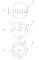
図14は、本発明にかかる膜厚測定装置の第5の実施の形態の要部を示す概略図である。同図(a)〜(c)は、いずれもウェーハ8の上方から見た平面図であり、複数のセンサの配置形態の典型例を示す。
【0157】
図14(a)は、渦電流損失測定センサ10を所定間隔で一つの列をなすように配置した例である。本例の場合は、同図の矢印A1に示すように、ウェーハ8をセンサの列に直交する方向に移動させるだけで、その表面に成膜される導電成膜9の全面を走査することができ、導電成膜9の膜厚分布を高速で測定できる。
【0158】
図14(b)は、十字をなすように、互いに直交する2つの方向へ渦電流損失測定センサ10を所定間隔で配置した例である。本例の場合では、十字形の中心に位置する渦電流損失測定センサ10がウェーハ8の中心の上方に位置するように、X−Y−Zステージ36を移動させた後、同図の矢印A2に示すように、時計方向または反時計方向に回動させるだけで、その表面に成膜される導電成膜9の全面を走査することができ、導電成膜9の膜厚分布を高速で測定できる。
【0159】
図14(c)は、渦電流損失測定センサ10を放射状に配置した例を示す。このように配置することにより、導電成膜9の膜厚測定上必要な領域の全てに渦電流損失測定センサ10が対応することとなり、一回の測定で導電成膜9の膜厚をほぼ全面にわたって測定することができる。従って、本例の場合では、成膜工程中にステージ36を移動させる必要がない。これにより、導電成膜9の膜厚を一括して測定できるので、膜厚分布を極めて高速で測定できる。この結果、極めて薄い導電成膜を成膜する場合で測定時間が限られている場合でも高い精度で一括測定が可能な膜厚測定装置が提供される。さらに、本実施形態と前述した第4の実施の形態と組み合わせて導電成膜9の上方および裏面側の双方で配置すれば、さらに多数の渦電流損失測定センサ10を一度に配置できることとなり、測定の速度および精度をさらに向上させることができる。
【0160】
(f)膜厚測定装置の第6の実施形態
次に、本発明にかかる膜厚測定装置の第6の実施形態について図15〜図17を参照しながら説明する。本実施形態の特徴は、渦電流損失測定センサをなす励起受信一体型コイルの中心軸と同軸上にレーザ変位センサを配置し、渦電流損失の測定と、渦電流損失測定センサと導電性膜の表面との距離の測定と、を同時に実現する点にある。
【0161】
図15は、本実施形態の膜厚測定装置の概略構成を示すブロック図である。図11に示す膜厚測定装置2との対比において明らかなように、図15に示す膜厚測定装置5は、光学式変位センサとしてレーザ変位センサ63を備え、また、光学式変位センサコントローラとしてレーザ変位センサコントローラ58を備える。さらに、膜厚測定装置2は、渦電流損失測定センサとして空芯型の励起受信一体型コイル68を備える。励起受信一体型コイル68とレーザ変位センサ63とは渦電流損失測定センサユニット60を構成する。膜厚測定装置2のその他の構成は、図11に示す膜厚測定装置2と実質的に同一である。本実施形態において、制御コンピュータ42とレーザ変位センサコントローラ58とステージ駆動部38とは、距離測定誤差補正手段を構成する。
【0162】
図16は、図15に示す膜厚測定装置5が備える渦電流損失測定センサユニット60の具体的構成を示す略示断面図である。レーザ変位センサ63は、レーザ発振部とレーザ受光部との中間点が励起受信一体型コイル68の中心軸と実質的に一致するように、励起受信一体型コイル68の上方に配設される。従って、レーザ発振部から出射したレーザ光LB1は、コイル68の空芯を経由して導電性膜9の表面に照射し、その反射光LB2も同様にコイル68の空芯を経由してレーザ受光部に入射する。これにより、レーザ変位センサ63と導電性膜との距離D1を表わす信号がレーザ変位センサコントローラ58を介して制御コンピュータ42に供給される。メモリ52内には、レーザ変位センサ63の下面とコイル68の下面との距離D2が予め格納されており、制御コンピュータ42は、距離D1から距離D2を除算することにより、渦電流損失測定センサユニット60と導電性膜9との間の距離DSFを算出する。
【0163】
上述した実施形態においては、光学式変位センサと渦電流損失測定センサとが導電性膜9と水平な方向に隣接していたので、光学式変位センサによる測定結果と、渦電流損失測定センサと導電性膜9間の実際の距離との間に誤差が生じる場合がある。これに対して、図15に示す渦電流損失測定センサユニット60は、コイル68の中心軸と導電性膜9の交点にほぼ一致する位置にレーザ光LB1を照射するので、渦電流損失測定センサユニット60と導電性膜9との間の距離DSFを正確に測定することができる。
【0164】
次に、図15に示す膜厚測定装置5を用いた膜厚測定方法について説明する。
【0165】
本実施形態の膜厚測定装置5は、上述した第1の測定方法から第3の測定方法のいずれの方法にもほぼ同様に適用することができる。ただし、上述したとおり、渦電流損失測定センサユニット60によれば、レーザ光LB1の導電性膜9への照射位置がコイルの中心線を導電性膜9の表面に下ろした交点の位置と実質的に一致するので、第1または第2の方法を本実施形態の膜厚測定装置5に適用した場合の特徴は、渦電流損失測定センサユニット60と導電性膜9との間の距離DSFの測定と、渦電流損失の測定とを同時に実行できる点にある。上述した実施形態では、光学式変位センサが渦電流損失測定センサから離隔して配設されるので、測定誤差を回避するため、その距離だけ渦電流損失測定センサを移動させなければならない。しかしその移動中におけるステージの振動や渦電流損失測定センサ自身の振動に起因して測定誤差が発生することがある。この一方、本実施形態によれば、渦電流損失測定センサユニット60と導電性膜9との間の距離DSFを直接測定できるので、このような測定誤差を回避できるうえ、ステージの動作回数を低減できるので、ステージの性能に対する負担を軽減することができる。これにより、さらに高精度でかつ高速の膜厚測定が可能になるとともに、膜厚測定装置の構成もさらに小型化、簡素化できる。
【0166】
ここで、本実施形態の膜厚測定装置5を用いて第3の測定方法による膜厚測定について図17を参照しながら説明する。
【0167】
まず、膜厚測定に先立って、導電性膜9における所望の膜厚測定範囲において予め定めた点数だけ、レーザ変位センサ63によりセンサユニット−導電性膜9間の距離DSFを測定しておく。この測定結果には、ウェーハの反りに起因する測定誤差が現われる。図17は、ウェーハ上の位置とセンサユニット−導電性膜9間の距離DSFとの関係の一例を示すグラフである。同図内のグラフlmに示すように、測定の結果、距離DSFは、激しく変化している。
【0168】
次に、制御コンピュータ42は、この測定結果に対して、スムージングや多項式近似等の処理を実行して測定誤差を除去し、その結果をメモリ52に格納する。図17に示すグラフlcは、グラフlmに現われた測定結果に対して実行した誤差処理の例を示す。
【0169】
次に、インピーダンスアナライザ49が供給する高周波電流の周波数fを設定する。即ち、導電性膜9を成膜するときの狙いの膜厚tを参照し、レシピファイル内の膜厚と分解能との関係を示すデータテーブル(図8参照)に基づいて最適と思われる周波数fを設定し、この周波数fを有する高周波電流を励起受信一体型コイル68に供給し、磁場を発生させる。この磁場により、導電性膜9に渦電流が励起され、前述した式1で表される渦電流損失Pが導電性膜9内に発生する。
【0170】
導電性膜9で渦電流損失Pが発生すると、導電性膜9の膜厚tに応じて渦電流損失測定センサユニット60のインピーダンス、励起受信一体型コイル68に流れる計測用の高周波電流の電流値または高周波電流の位相が変化する(図9参照)。
【0171】
この変化をインピーダンスアナライザ49がモニタして制御コンピュータ42に供給する。制御コンピュータ42の膜厚演算部54は、予め作成されレシピファイルに書き込まれた、膜厚tと膜の抵抗値との関係を示すデータテーブルと、測定誤差除去処理後のセンサユニット−導電性膜9間の距離DSFの変化のデータテーブルとを参照しながら膜厚tを演算して出力する。
【0172】
膜厚測定装置5は、以上の膜厚測定をウェーハ8の所望の測定範囲における所定の点数だけ実行する。ここで、誤差を低減させるためのプレスキャンにより近似関数が既に得られているので、渦電流の測定における測定点は、プレスキャンの測定点と一致する必要がない。膜厚演算部54は、予め得られた近似関数を参照しながら導電性膜9の膜厚tを算出する。
【0173】
上述した第3の膜厚測定方法によれば、レーザ変位センサ63を用いてセンサユニット−導電性膜9間の距離DSFの変化のデータテーブルを予め取得し、このデータテーブルから測定誤差が除去された近似関数を用いて膜厚を算出するので、渦電流損失の測定点数を必要最小限に止めながら、光学式変位センサの精度が比較的低いという問題を解消することができる。これにより、LSIパターン上の反射率が大きい導電性膜や表面が荒れた導電性膜に対する変位測定精度の劣化を抑制できるので、上述した第3の膜厚測定方法は、ウェーハ毎の変位測定が必要でない場合、例えば同一ロット内のウェーハ、同一の回路パターンが形成されたウェーハまたは同一プロセスを経たウェーハなど、ウェーハの反りが互いに大きく異なることがない場合に特に有効である。なお、本実施形態では、X−Y−Zステージ36を備える場合について説明したが、ウェーハ8の搬送中など、X−Y−Zステージ36を利用できない場合であっても、例えばロボットアームが渦電流損失測定センサユニット60の下方でウェーハを乗せて移動することにより、導電性膜9の膜厚測定は可能である。
【0174】
(g)膜厚測定装置の第7の実施形態
次に、本発明にかかる膜厚測定装置の第7の実施形態について図18を参照しながら説明する。本実施形態は、図15に示す膜厚測定装置5において、渦電流損失測定センサユニット60を導電性膜9の裏面側に配置した形態である。
【0175】
図18は、本実施形態の膜厚測定装置の要部を示す概略図である。同図(a)に示すように、本実施形態の膜厚測定装置5’は、半導体ウェーハ8の裏面側、即ち、導電性膜9が成膜された面と反対面側に配置された渦電流損失測定センサユニット60と、このセンサを上面にて支持するZ−ステージ35を備える。また、膜厚測定装置5’は、図13に示す第4の実施形態と同様に、X−Y−Zステージ36に代えて半導体ウェーハ8をその周辺部から支持するX−Y−Zステージ37を備える。膜厚測定装置5’のその他の構成は、図15に示す膜厚測定装置5と実質的に同一である。
【0176】
このような構成により、本実施形態の膜厚測定装置5’は、ウェーハ8の裏側に配置された励起受信一体型コイル68によって高周波磁界を励磁し、ウェーハ8を介して導電性膜9に渦電流を発生させ、発生した渦電流により変化した合成磁界を検出して導電性膜9の膜厚を測定する。また、センサユニット−導電性膜間の距離DSFは、ウェーハ8の裏面と渦電流損失測定センサユニット60との距離D3とウェーハ8の厚さTsとを予め取得しておけば、距離(D3+Ts)により算出できる。
【0177】
また、例えば図18(b)に示すように、ウェーハ8の裏面に渦電流損失測定センサユニット60の上面を接触させて測定することも可能である。この場合、変位を測定する必要はない。
【0178】
このように、本実施形態の膜厚測定装置5’によれば、ウェーハ8の裏面側に渦電流損失測定センサユニット60を配置するので、成膜工程やエッチング工程においてウェーハ8上に成膜される導電成膜9の成膜などを妨げるおそれが解消する。さらに、CMP研磨工程においては、研磨用ツールとの接触を回避しながら測定する必要もなくなる。これにより、測定上の制約が大幅に減少するので、成膜工程、研磨工程またはエッチング工程などの製造工程においてリアルタイムで膜厚を測定するIn−situ型の膜厚測定装置として動作させることができる。このように本実施形態によれば、設計の自由度並びに測定の精度およびスループットのいずれについても優れた膜厚測定装置が提供される。膜厚測定装置5’の具体的な測定方法は、上述した第1から第3の測定方法と実質的に同一である。
【0179】
なお、本実施形態では、ウェーハの裏面側にのみ渦電流損失測定センサユニットを配置した形態について説明したが、図13に示す第4の実施形態と同様に、導電成膜9の裏面側に加えて上方側にも渦電流損失測定センサユニット60を配置し、両側から膜厚を測定することとしても良い。
【0180】
(h)膜厚測定装置の第8の実施形態
次に、本発明にかかる膜厚測定装置の第8の実施の形態について図19および図20を参照しながら説明する。本実施形態の特徴は、上述した光学式変位センサまたはレーザ変位センサに代えて静電容量式変位センサを備え、これによりセンサユニット−導電性膜間の距離を測定する点にある。
【0181】
図19は、本実施形態の膜厚測定装置の概略構成を示すブロック図である。同図に示す膜厚測定装置6は、上述した第2〜第7の実施形態と同様に、X−Y−Zステージ36と、ステージ駆動部38と、インピーダンスアナライザ49と、制御コンピュータ42と、を備える他、本実施形態において特徴的な渦電流損失測定センサユニット70と静電容量式変位センサコントローラ88をさらに備える。
【0182】
渦電流損失測定センサユニット70は、渦電流損失測定センサとして励起受信一体型コイル12と、励起受信一体型コイル12を覆うように形成された絶縁部材126と、静電容量式変位センサ電極72とを含む。コイル12は、インピーダンスアナライザ49から高周波電流の供給を受けて高周波磁界を形成し、導電性膜9に局所的に渦電流を発生させるとともに、この渦電流により発生した磁界とコイル12により発生した磁界との合成磁界を受信する。
【0183】
静電容量式変位センサコントローラ88は、渦電流損失測定センサユニット70内の静電容量式変位センサ電極72に接続されるとともに、配線G1によりグランドに接続される。また、ウェーハ8はその側面側で配線G3によりグランドに接続される。これにより、導電性膜9もグランド電位に保持される。この結果、静電容量式変位センサ電極72と導電性膜9とはコンデンサの両側の電極をなし、静電容量式変位センサコントローラ88は、静電容量式変位センサ電極72−導電性膜9間の静電容量を測定し、その測定結果を制御コンピュータ42に供給する。制御コンピュータ42は、静電容量式変位センサコントローラ88の測定結果から静電容量式変位センサ電極72−導電性膜9間の距離を算出する。なお、図19に示すように、ウェーハ8の側面をグランドに接続することに代え、導電性膜9の表面領域のうち膜厚測定に影響を及ぼさない部位、例えば端部を配線G4を介してグランド接続しても良く、またはX−Y−Zステージ36を貫通する配線G2によりその端部の裏面側でグランドに接続しても良い。図19においては、導電性膜9をグランド電位に保持するための配線としてG2〜G4を示したが、これらは代替的であり、測定環境に応じて適宜選択できる。例えば、導電性膜9を直接グランドに接続する態様を選択すれば、ウェーハ8の搬送中など、X−Y−Zステージ36を利用できない場合であっても測定が可能になる。
【0184】
静電容量式変位センサ電極72の具体的構成について図20を参照しながら説明する。
【0185】
図20(a)は、図19に示す渦電流損失測定センサユニット70の略示断面図であり、また、図20(b)は、渦電流損失測定センサユニット70の底面図である。静電容量式変位センサ電極72は、高抵抗材料で形成された厚さTeのリング状薄膜電極であり、励起受信一体型コイル12を周回するように絶縁部材126の底部に配設される。本実施形態において、静電容量式変位センサ電極72のリング形状の中心軸は、コイル12の中心軸と一致している。センサ電極72の厚さTeは、本実施形態において約10〜50μmである。また、絶縁部材の底部周辺にはセンサ電極72の厚さTeに応じた深さを有する凹部が設けられ、センサ電極72は、その表面がコイル12の底面と同一平面内に位置するように、この凹部に嵌設される。これにより、静電容量式変位センサにより測定された距離が、コイル12−導電性膜9間の距離DSFと一致する。
【0186】
静電容量式変位センサ電極72の外径EDの大きさは、コイル12により渦電流が励起された領域の直径と実質的に同一になるように選択される。これにより、渦電流損失を測定した領域全般にわたって、センサ電極72から検出された静電容量値が平均化されるので、コイル12−導電性膜9間の距離DSFの測定精度が向上し、この結果、膜厚測定の精度も向上する。本実施形態において、外径EDは、約6〜16mmである。さらに、静電容量式変位センサ電極72の内径IDの大きさは、コイル12により励磁された高周波磁界が静電容量の測定精度に影響を与えない程度に電極72の内周面とコイル12の外周面とが十分に離隔し、かつ、静電容量の測定にあたり電極の表面積が十分な大きさとなるように選択される。本実施形態においてコイル12の外周面と電極72の内周面との距離は、約1〜2mmである。なお、本実施形態の渦電流損失測定センサユニット70においては、コイル12のコア内にも絶縁材料が充填されて絶縁部材126の一部を構成しているが、図16に示す渦電流損失測定センサユニット60と同様に空芯の構造としても良い。
【0187】
本実施形態の膜厚測定装置6を用いた膜厚測定方法は、第1から第6の実施形態にて説明した第1および第2の測定方法とほぼ同一であるが、本実施形態の特徴は、渦電流損失の測定とコイル12−導電性膜9間の距離DSFの測定とを同時に実行できる点にある。従って、X−Y−Zステージ36の振動や渦電流損失測定センサユニット70の振動に起因するコイル12−導電性膜9間の距離DSFの測定誤差を大幅に低減できる。この結果、高精度でかつ高速の膜厚測定を実現できるので、測定のスループットがさらに向上する。また、ステージの移動回数が減少するので、ステージ性能に対する負担をも低減でき、膜厚測定装置の構成もさらに小型化、簡素化できる。さらに、静電容量を用いてコイル12−導電性膜9間の距離DSFを測定するので、導電性膜9の表面反射率や表面のラフネスの影響を受けない。これにより、LSIパターン上に形成された導電性膜に対してもコイル12との距離を高精度で測定することができる。
【0188】
(i)膜厚測定装置の第9の実施形態
次に、本発明にかかる膜厚測定装置の第9の実施の形態について図21を参照しながら説明する。本実施形態の膜厚測定装置6’の特徴は、渦電流損失測定センサユニット70’が備える静電容量式変位センサ電極74の形状にある。膜厚測定装置6’のその他の構成は、図20に示す膜厚測定装置6と同一であるので、以下では相異点のみを説明する。
【0189】
図21(a)は、本実施形態膜厚測定装置6’が備える渦電流損失測定センサユニット70’の略示断面図であり、また、図20(b)は、渦電流損失測定センサユニット70’の底面図である。同図(b)に示すように、渦電流損失測定センサユニット70’に配設された静電容量式変位センサ電極74は、円弧状の4つの電極片74a〜74dで構成され、これらの電極片がコイル12を周回するリングをなすように配設される。
【0190】
本実施形態によれば、複数の電極片でセンサ電極を構成するので、コイル12により励磁された磁界によりセンサ電極内に渦電流が発生することを防止することができる。これにより、膜厚測定の精度をさらに向上させることができる。
【0191】
本実施形態の膜厚測定装置6’を用いた膜厚測定方法は、前述した第8の実施形態と同一であるので、その説明は省略する。
【0192】
(j)膜厚測定装置の第10の実施形態
次に、本発明にかかる膜厚測定装置の第10の実施形態について図22を参照しながら説明する。
【0193】
本実施形態は、図19に示す膜厚測定装置6において、渦電流損失測定センサユニット70を導電性膜9の裏面側に配置した形態である。
【0194】
図22は、本実施形態の膜厚測定装置の要部を示す概略図である。同図(a)に示すように、本実施形態の膜厚測定装置6’’は、半導体ウェーハ8の裏面側、即ち、導電性膜9が成膜される面と反対面側に配置された渦電流損失測定センサユニット70と、このセンサを上面にて支持するZ−ステージ35を備える。また、膜厚測定装置6’’は、図13に示す第4の実施形態と同様に、X−Y−Zステージ36に代えて半導体ウェーハ8をその周辺部から支持するX−Y−Zステージ37を備える。膜厚測定装置6’’のその他の構成は、図19に示す膜厚測定装置5と実質的に同一である。また、膜厚測定装置6’’の具体的な測定方法は、第9の実施形態において前述した測定方法と実質的に同一である。
【0195】
このような構成により、本実施形態の膜厚測定装置6’’は、ウェーハ8の裏側に配置された励起受信一体型コイル12によって高周波磁界を励磁し、ウェーハ8を介して導電性膜9に渦電流を発生させ、発生した渦電流により変化した合成磁界を検出して導電性膜9の膜厚を測定する。また、センサユニット−導電性膜間の距離DSFは、ウェーハ8の裏面と渦電流損失測定センサユニット60との距離D3とウェーハ8の厚さTsとを予め取得しておけば、距離(D3+Ts)により容易に算出できる。
【0196】
また、例えば図22(b)に示すように、ウェーハ8の裏面に渦電流損失測定センサユニット70の上面を接触させて測定することも可能である。
【0197】
このように、本実施形態の膜厚測定装置6’’によれば、ウェーハ8の裏側に渦電流損失測定センサユニット70を配置するので、成膜工程やエッチング工程においてウェーハ8上に成膜される導電成膜9の成膜などを妨げるおそれが解消する。さらに、CMP研磨工程においては、研磨用ツールとの接触を回避しながら測定する必要もなくなる。これにより、測定上の制約が大幅に減少するので、本実施形態の膜厚測定装置6’’はIn−situ型の膜厚測定装置として動作させることができる。このように本実施形態によれば、設計の自由度並びに測定の精度およびスループットのいずれについても優れた膜厚測定装置が提供される。
【0198】
なお、本実施形態では、ウェーハの裏面側にのみ渦電流損失測定センサユニット70を配置した形態について説明したが、図13に示す第4の実施形態と同様に、導電成膜9の裏面側に加えて上方側にも渦電流損失測定センサユニット70を配置し、両側から膜厚を測定することとしても良い。
【0199】
(3)記録媒体
上述した一連の測定手順は、第1〜第3の測定方法を含め、コンピュータに実行させるプログラムとしてフロッピーディスクやCD−ROM等の記録媒体に収納し、コンピュータに読込ませて実行させても良い。これにより、変位センサと汎用の制御コンピュータとを備える膜厚測定装置を用いて上述した膜厚測定方法を実現することができる。記録媒体は、磁気ディスクや光ディスク等の携帯可能なものに限定されず、ハードディスク装置やメモリなどの固定型の記録媒体でも良い。また、上述した膜厚測定方法の一連の手順を組込んだプログラムをインターネット等の通信回線(無線通信を含む)を介して頒布しても良い。さらに、上述した膜厚測定方法の一連の手順を組込んだプログラムを暗号化したり、変調をかけたり、圧縮した状態で、インターネット等の有線回線や無線回線を介して、あるいは記録媒体に収納して頒布しても良い。
【0200】
以上、本発明の実施の形態について説明したが、本発明は、上記形態に限ることなく、その要旨を逸脱しない範囲で種々変形して適用することができる。例えば、上述した膜厚測定装置の実施の形態においては、第4の実施形態において渦電流損失測定センサ20を用いた形態について説明したが、図1に示す電流損失測定センサ10を用いても、図12に示す電流損失測定センサ120を用いても良い。同様に、第5の実施形態において電流損失測定センサ10を用いた形態について説明したが、図2に示す電流損失測定センサ20を用いても、また、図12に示す電流損失測定センサ120を用いても良い。また、これら3つの形態の電流損失測定センサを同一装置内で適宜組み合わせて用いても良い。さらに、第6〜第10の実施形態においては、励起受信一体型のコイルを有する渦電流損失測定センサユニットについて説明したが、渦電流励起コイルと受信コイルとを有する渦電流損失測定センサユニットにも適用できることは明らかである。また、第6〜第10の実施形態では、単一の渦電流損失測定センサユニットを備える場合について説明したが、図14に示すように、複数のセンサユニットを配置しても良いことは勿論である。
【0201】
【発明の効果】
以上詳述したとおり、本発明は、以下の効果を奏する。
【0202】
即ち、本発明にかかる渦電流損失測定センサによれば、測定対象である導電性膜との対向面において高周波磁界励磁コイルの少なくとも一部の領域が露出するように、上記導電性膜との対向面に開口が形成された第2の透磁性部材を備えるので、この開口からのみ磁束が集中的に外部へ漏れ出すように磁路を制御できる。これにより、上記導電性膜の微小領域に磁場を集中させることができ、上記導電性膜において渦電流を局所的に励起させることができる。これにより、受信コイルから得られる出力電流から渦電流損失測定センサのインピーダンスの変化、上記高周波電流の電流値の変化または上記高周波電流の位相の変化を測定することにより渦電流損失を測定できるので、上記導電性膜の膜厚を高い精度で測定することができる。
【0203】
また、本発明にかかる膜厚測定装置によれば、渦電流損失測定センサと導電性膜との距離を測定する距離測定手段と、この上記距離測定手段の測定結果と渦電流損失測定手段の測定結果に基づいて上記導電性膜の膜厚を算出する膜厚演算手段とを備えるので、上記距離に依存する測定誤差を減少させることができる。これにより、高い精度で導電性膜の膜厚を測定することができる。
【0204】
本発明にかかる膜厚測定装置において、本発明にかかる渦電流損失測定センサを備える場合は、上記効果に加え、局所的に上記導電性膜の膜厚を管理できるので、例えば表面にパターンが設けられたウェーハ上に成膜された導電性膜など、比較的膜厚のばらつきが大きな被測定物であっても、高い精度で膜厚を測定することができ、CMPやメッキ装置など、多様な装置内で膜厚を管理することが可能になる。
【0205】
また、本発明にかかる膜厚測定装置において、励起受信一体型の空芯コイルまたは空芯の受信コイルの上方に設けられたレーザ変位センサを上記距離測定手段が含む場合は、上記渦電流損失測定センサと上記導電性膜との上記距離の測定と渦電流損失の測定とを同時を実行できるので、より優れた精度で高いスループットの膜厚測定が可能になる。
【0206】
また、本発明にかかる膜厚測定装置において、上記距離測定手段が上記渦電流損失測定センサに近接して設けられた電極を有する有静電容量式変位センサを含む場合は、上記距離の測定と渦電流損失の測定とを同時を実行できるうえ、上記導電性膜の表面における光の反射率や表面のラフネスの影響を受けることなく上記距離をより正確に測定することができる。
【0207】
また、本発明にかかる膜厚測定方法によれば、上記渦電流損失測定センサおよび上記導電性膜間の距離を測定する距離測定工程と、この距離測定工程により得られた上記距離と、渦電流損失測定工程により得られたインピーダンスの変化または高周波電流の電流値の変化または上記高周波電流の位相の変化とに基づいて上記導電性膜の膜厚を算出する膜厚算出工程とを備えるので、非接触・非破壊の態様で高精度の膜厚測定を実現できる。
【0208】
本発明にかかる膜厚測定方法において、上記距離測定手段が上記変位センサまたは上記静電容量式変位センサを備え、上記距離測定工程と、上記渦電流損失測定工程とが並行して同時に実行される場合は、より高い精度で、かつ、より優れたスループットで膜厚を測定することができる。
【0209】
さらに、本発明にかかる記録媒体によれば、上記距離測定手段と汎用のコンピュータとを備えた膜厚測定装置を用いて導電性膜を高精度かつ高速で測定することができる。
【図面の簡単な説明】
【図1】本発明にかかる渦電流損失測定センサの第1の実施の形態の概略構成を示す断面図と底面図である。
【図2】渦電流センサから発生した磁束密度の分布をシミュレーションにより求めたグラフである。
【図3】本発明にかかる渦電流損失測定センサの第2の実施の形態の概略構成を示す断面図と底面図である。
【図4】本発明にかかる膜厚測定装置の第1の実施の形態の概略構成を示すブロック図である。
【図5】渦電流センサおよび導電性膜間の距離と、渦電流センサのインダクタンスおよび抵抗の変化との関係を測定した実験データを示すグラフである。
【図6】導電性膜の膜厚の変化と、渦電流センサのインダクタンスおよび抵抗の変化との関係を測定した実験データを示すグラフである。
【図7】膜厚の測定誤差を補正する方法を説明するグラフである。
【図8】膜厚と測定装置の分解能との関係を高周波電流の周波数をパラメータとして測定した実験データを示すグラフである。
【図9】導電性膜の膜厚が変化した時の渦電流損失測定センサのインダクタンスと抵抗値の変化を測定した実験データを示すグラフである。
【図10】図4に示す膜厚測定装置により、導電性材料を含む回路パターンまたは下地導電性膜の上に成膜された導電性膜を測定する方法を示す略示断面図である
【図11】本発明にかかる膜厚測定装置の第2の実施の形態の概略構成を示すブロック図である。
【図12】本発明にかかる膜厚測定装置の第3の実施の形態が備える渦電流損失測定センサの概略構成を示す断面図である。
【図13】本発明にかかる膜厚測定装置の第4の実施の形態の要部を示す概略図である。
【図14】本発明にかかる膜厚測定装置の第5の実施の形態の要部を示す概略図である。
【図15】本発明にかかる膜厚測定装置の第6の実施形態の概略構成を示すブロック図である。
【図16】図15に示す膜厚測定装置が備える渦電流損失測定センサユニットの具体的構成を示す断面図と底面図である。
【図17】図15に示す膜厚測定装置を用いた膜厚測定方法を説明するグラフである。
【図18】本発明にかかる膜厚測定装置の第7の実施形態の要部を示す概略図である。
【図19】本発明にかかる膜厚測定装置の第8の実施形態の概略構成を示すブロック図である。
【図20】図19に示す渦電流損失測定センサユニットの具体的構成を示す断面図と底面図である。
【図21】本発明にかかる膜厚測定装置の第9の実施形態が備える渦電流損失測定センサユニットの具体的構成を示す断面図と底面図である。
【図22】本発明にかかる膜厚測定装置の第10の実施形態の要部を示す概略図である。
【図23】従来の技術による膜厚測定方法の一例を説明するグラフである。
【図24】従来の技術による膜厚測定方法の他の例を説明するブロック図である。
【図25】従来の技術による渦電流センサの一例を示す断面図および底面図である。
【図26】従来の技術による変位センサの一例を示す説明図である。
【符号の説明】
1〜4,4’、4’’,5,5’,6,6’,6’’ 膜厚測定装置
8 半導体ウェーハ(基板)
9 導電性膜
10,20,30,120 渦電流損失測定センサ
12 励起受信一体型コイル
14 フェライト(透磁性部材)
15 磁性材料メッキ
16 開口部
19 下地回路パターンまたは下地導電性膜
22 受信コイル
24 渦電流励起コイル
32 光学式変位センサ
34,35 Zステージ
36 X−Y−Zステージ
38 ステージ駆動部
42 制御コンピュータ
44 高周波電源
46 光学式変位センサコントローラ
48,49 インピーダンスアナライザ
52 メモリ
54 膜厚演算部
58 レーザ変位センサコントローラ
60,70,70’ 渦電流損失測定センサユニット
63 レーザ変位センサ
68 励起受信一体型コイル(空芯コイル)
72,74 静電容量式変位センサ電極
88 静電容量式変位センサ[0001]
BACKGROUND OF THE INVENTION
The present invention relates to a film thickness measuring apparatus, and more particularly to an eddy current measurement for measuring an eddy current loss due to an eddy current excited in a conductive film on a wafer surface by exciting a high-frequency magnetic field in a manufacturing process of a semiconductor integrated circuit device. The present invention is directed to a sensor, a measuring apparatus that measures the film thickness of the conductive film in a non-contact manner based on the measured eddy current loss, a film thickness measuring method, and a computer-readable recording medium.
[0002]
[Prior art]
The method of measuring the film thickness of a conductive film using eddy current is effective as a non-contact and non-destructive film thickness measurement technique.
[0003]
In the film thickness measurement method using eddy current, the distance between the coil (sensor) that generates a magnetic field and the conductive film strongly affects the amount of eddy current loss in the conductive film. For this reason, it is important to control the distance between the sensor and the conductive film with high accuracy.
[0004]
FIG. 23 shows data of an experimental example in which the amount of eddy current loss is measured as changes in the inductance and resistance of the sensor. It can also be seen from the figure that the inductance and resistance of the sensor change according to the distance between the sensor and the conductive film.
[0005]
In order to reduce measurement errors due to such distance dependency and improve measurement accuracy, the following techniques have been proposed.
[0006]
For example, as a first method, as shown in FIG. 23, a correlation between the distance between the sensor and the conductive film and the measured value is obtained in advance, and the distance between the sensor and the conductive film is changed to obtain a plurality of points. There is a method of performing correction using the above correlation for each measurement point after measurement.
[0007]
As a second method, as shown in FIG. 24,
[0008]
[Problems to be solved by the invention]
However, the second measurement method described above has a drawback that the configuration of the apparatus becomes complicated and large.
[0009]
In the first method of measuring multiple points at different distances, the sensor or stage must be operated as many times as the number of measurements, and data processing must be performed for each measurement point, requiring enormous measurement time. It becomes. Therefore, it is unsuitable for high-speed measurement required in a mass production line or real-time measurement in a film thickness forming process, and there is a problem that it is not practical.
[0010]
On the other hand, in order to enable local film thickness measurement and improve measurement accuracy, an attempt to concentrate the magnetic field generated by the coil at one point is shown in FIG. 25 in addition to a method of increasing the resolution by reducing the coil diameter. As described above, only the method of inserting the
[0011]
As a sensor for measuring the displacement of a metal conductor, a sensor that concentrates a magnetic field on the conductor has been proposed. One example will be described with reference to FIG.
[0012]
As shown in FIG. 26A, the displacement sensor shown in FIG. 26 includes a
[0013]
The high frequency
[0014]
The outer shielding plate 114 is composed of
[0015]
When a high-frequency excitation current is passed through the high-
[0016]
As described above, the structure in which the magnetic flux is emitted to the vertically long region by the linear or cross-shaped slit is effective for examining the displacement of an elongated object such as a metal conductor, but is used for local film thickness measurement. Is insufficient because it is necessary to form a magnetic field as a spot.
[0017]
The present invention has been made in view of the above circumstances, and its purpose is to enable local film thickness measurement.Eddy current loss measurement sensorIs to provide.
[0018]
[Means for Solving the Problems]
The present invention aims to solve the above problems by the following means.
[0019]
That is, according to the first aspect of the present invention,
A cylindrical excitation receiver that receives a high-frequency current to excite a high-frequency magnetic field to excite an eddy current in a conductive film to be measured and receive a combined magnetic field of the magnetic field generated by the eddy current and the high-frequency magnetic field. Body coil,
A circle formed of a first magnetically permeable material and inserted into the excitation receiving integrated coil to form a corePillarA first magnetically permeable member having a shape;
A region formed of a second magnetically permeable material and provided so as to enclose the first magnetically permeable member and the excitation / reception integrated coil, and a partial region of the excitation / reception integrated coil on a surface facing the conductive film A second magnetically permeable member having an annular opening formed around the first magnetically permeable member so that only the first magnetically permeable member is exposed;
With,
The opposing surface of the first magnetically permeable member facing the conductive film and the opposing surface of the second magnetically permeable member facing the conductive film are arranged in the same plane.
Non-contact typeAn eddy current loss measurement sensor is provided.
[0021]
According to the second aspect of the present invention,
A cylindrical eddy current exciting coil that receives a high frequency current to excite a high frequency magnetic field to excite the eddy current in the conductive film to be measured;
A cylindrical receiving coil that is provided to be circulated by the eddy current excitation coil in the eddy current excitation coil, and that receives a combined magnetic field of the magnetic field generated by the eddy current and the high frequency magnetic field;
A circle formed of a first magnetically permeable material and inserted into the receiving coil to form a corePillarA first magnetically permeable member having a shape;
A region formed of a second magnetically permeable material and provided so as to wrap around the first magnetically permeable member, the receiving coil, and the eddy current exciting coil, and a partial region of the receiving coil on a surface facing the conductive film A second magnetically permeable member having an annular opening formed around the first magnetically permeable member so that only the first magnetically permeable member is exposed;
With,
The opposing surface of the first magnetically permeable member facing the conductive film and the opposing surface of the second magnetically permeable member facing the conductive film are arranged in the same plane.
Non-contact typeAn eddy current loss measurement sensor is provided.
[0087]
DETAILED DESCRIPTION OF THE INVENTION
Hereinafter, some embodiments of the present invention will be described with reference to the drawings. In the following drawings, the same portions are denoted by the same reference numerals, and the description thereof is omitted as appropriate.
[0088]
(1) Embodiment of sensor for measuring eddy current loss
First, some embodiments of the eddy current loss measuring sensor according to the present invention will be described.
[0089]
(A) First embodiment of sensor for measuring eddy current loss
FIG. 1A is a schematic cross-sectional view showing a first embodiment of an eddy current loss measuring sensor according to the present invention, and FIG. 1B is a bottom view thereof.
[0090]
As shown in FIG. 1A, an eddy current
[0091]
The
[0092]
Both the
[0093]
The feature of the eddy current loss measuring sensor of this embodiment is that an
[0094]
The operation of the eddy current
[0095]
When a high frequency current is supplied to the
[0096]
Therefore, if the eddy current
[0097]
FIG. 2 is a graph obtained by simulating the magnetic flux density distributed on the surface of the
[0098]
As described above, according to the eddy current
[0099]
(B) Second embodiment of sensor for measuring eddy current loss
Next, a second embodiment of the eddy current loss measuring sensor according to the present invention will be described with reference to FIG.
[0100]
FIG. 3A is a schematic cross-sectional view showing the eddy current
[0101]
As described above, according to the present embodiment, since two coils having different functions are used for eddy current excitation and eddy current loss reception, an eddy current loss measurement sensor having higher resolution can be provided. .
[0102]
In the two embodiments described above, the
[0103]
(2) Embodiment of film thickness measuring device
Next, some embodiments of the film thickness measuring device according to the present invention will be described with reference to the drawings.
[0104]
(A) First embodiment of film thickness measuring apparatus
FIG. 4 is a block diagram showing a schematic configuration of the first embodiment of the film thickness measuring apparatus according to the present invention. As shown in the figure, the film
[0105]
The
[0106]
The
[0107]
The
[0108]
The
[0109]
The high
[0110]
The eddy
[0111]
The
[0112]
The
[0113]
The
[0114]
The measurement data includes a distance D between the eddy current loss measurement sensor and the conductive film 9.SF, The change in impedance of the eddy current loss measurement sensor affected by the eddy current loss with respect to the frequency f of the current supplied from the high
[0115]
The
[0116]
5 and 6 show specific examples of the measurement data table included in the recipe file. FIG. 5 shows a distance D between the eddy current
[0117]
The
[0118]
A film thickness measuring method using the film
[0119]
The film
[0120]
As a method for measuring the film thickness, a first measurement method in which the distance between the
[0121]
The first measurement method includes a process of operating both the
[0122]
The film
[0123]
During measurement, a value serving as a measurement reference (hereinafter referred to as a reference value) is sequentially measured to correct a measurement error (first correction process). This is because the measured value drifts because the temperature around the film
[0124]
First, the frequency f of the high frequency current supplied by the high
[0125]
FIG. 8 shows an example in which the relationship between the film thickness t (μm) of the
[0126]
The high-frequency current having the frequency f set in this way is supplied to the eddy current
[0127]
P = (f2・ T) / ρ ・ ・ ・ ・ ・ ・ (1)
Here, the resistivity ρ of the
[0128]
When such eddy current loss P occurs in the
[0129]
FIG. 9 shows an example of measuring changes in the inductance and resistance values of the eddy current loss measurement sensor when the film thickness t of the
[0130]
The
[0131]
The film
[0132]
When a pattern is formed on the surface of the
[0133]
In the above-described embodiment, the reference value is sequentially measured during the measurement in the region where the conductive film is not formed, and the measurement error is corrected based on the reference value. However, the reference value and the measuring method thereof are not limited to the above-described form. For example, a conductive film having a predetermined thickness is formed in advance in a region that is free from the influence of eddy currents, and the
[0134]
Here, the
[0135]
In the film
[0136]
(B) Second embodiment of film thickness measuring apparatus
FIG. 11 is a block diagram showing a schematic configuration of the second embodiment of the film thickness measuring apparatus according to the present invention. The film
[0137]
The control method of the film
[0138]
In the measurement, as in the first measurement method described above, the measurement reference value is sequentially measured during the measurement, and the measurement error is corrected (first correction process). In addition, as described above, instead of sequentially measuring the reference value during the measurement, one or more reference values are obtained from the measurement conductive film formed in advance before the measurement, and based on this. Measurement errors may be corrected.
[0139]
In starting the measurement, first, the frequency f of the high frequency current is set based on the designed film thickness value and the data table in the recipe file.
[0140]
Next, the high-frequency current having the frequency f set in this way is supplied from the
[0141]
Under the influence of the eddy current loss due to the eddy current, the impedance of the
[0142]
The
[0143]
In the present embodiment, the film
[0144]
Further, the
[0145]
Thus, according to the film
[0146]
(C) Third embodiment of film thickness measuring apparatus
Next, a third embodiment of the film thickness measuring apparatus according to the present invention will be described with reference to the drawings.
[0147]
The film
[0148]
The eddy current
[0149]
The eddy current
[0150]
As described above, according to the present embodiment, the amount of eddy current loss can be measured even using a conventional eddy current loss measurement sensor, and therefore the film thickness t of the conductive film can be measured by the above-described measurement procedure. . The measurement method may be either the first measurement method or the second measurement method described above.
[0151]
(D) Fourth embodiment of film thickness measuring apparatus
Next, a fourth embodiment of the film thickness measuring apparatus according to the present invention will be described with reference to the drawings.
[0152]
FIG. 13 is a schematic view showing a main part of the film thickness measuring apparatus according to the present embodiment. As shown in FIG. 5A, the film
[0153]
With such a configuration, the film
[0154]
As described above, since the eddy current
[0155]
(E) Fifth embodiment of film thickness measuring apparatus
Next, a fifth embodiment of the film thickness measuring apparatus according to the present invention will be described with reference to the drawings. A feature of the film
[0156]
FIG. 14 is a schematic view showing a main part of a fifth embodiment of the film thickness measuring apparatus according to the present invention. FIGS. 7A to 7C are plan views as viewed from above the
[0157]
FIG. 14A shows an example in which the eddy current
[0158]
FIG. 14B is an example in which the eddy current
[0159]
FIG. 14C shows an example in which the eddy current
[0160]
(F) Sixth embodiment of film thickness measuring apparatus
Next, a sixth embodiment of the film thickness measuring apparatus according to the present invention will be described with reference to FIGS. The feature of this embodiment is that a laser displacement sensor is arranged coaxially with the central axis of the excitation-reception integrated coil forming the eddy current loss measurement sensor, and the eddy current loss measurement, eddy current loss measurement sensor, and conductive film It is in the point of realizing the measurement of the distance to the surface at the same time.
[0161]
FIG. 15 is a block diagram showing a schematic configuration of the film thickness measuring apparatus of the present embodiment. As is clear from comparison with the film
[0162]
FIG. 16 is a schematic cross-sectional view showing a specific configuration of the eddy current loss measuring
[0163]
In the embodiment described above, since the optical displacement sensor and the eddy current loss measurement sensor are adjacent to the
[0164]
Next, a film thickness measuring method using the film
[0165]
The film
[0166]
Here, film thickness measurement by the third measurement method using the film
[0167]
First, prior to film thickness measurement, the distance D between the sensor unit and the
[0168]
Next, the
[0169]
Next, the frequency f of the high frequency current supplied by the
[0170]
When an eddy current loss P occurs in the
[0171]
This change is monitored by the
[0172]
The film
[0173]
According to the third film thickness measurement method described above, the distance D between the sensor unit and the
[0174]
(G) Seventh embodiment of film thickness measuring apparatus
Next, a seventh embodiment of the film thickness measuring apparatus according to the present invention will be described with reference to FIG. This embodiment is a form in which the eddy current loss
[0175]
FIG. 18 is a schematic view showing a main part of the film thickness measuring apparatus according to the present embodiment. As shown in FIG. 5A, the film
[0176]
With such a configuration, the film
[0177]
Further, for example, as shown in FIG. 18B, the measurement can be performed by bringing the upper surface of the eddy current loss measuring
[0178]
As described above, according to the film
[0179]
In the present embodiment, the eddy current loss measurement sensor unit is disposed only on the back side of the wafer. However, in the same manner as the fourth embodiment shown in FIG. Further, the eddy current loss
[0180]
(H) Eighth Embodiment of Film Thickness Measuring Device
Next, an eighth embodiment of the film thickness measuring apparatus according to the present invention will be described with reference to FIGS. The feature of this embodiment is that a capacitance type displacement sensor is provided in place of the optical displacement sensor or the laser displacement sensor described above, thereby measuring the distance between the sensor unit and the conductive film.
[0181]
FIG. 19 is a block diagram showing a schematic configuration of the film thickness measuring apparatus of the present embodiment. As in the second to seventh embodiments described above, the film
[0182]
The eddy current loss
[0183]
The capacitance type
[0184]
A specific configuration of the capacitive
[0185]
FIG. 20A is a schematic cross-sectional view of the eddy current loss
[0186]
The size of the outer diameter ED of the capacitive
[0187]
The film thickness measuring method using the film
[0188]
(I) Ninth embodiment of film thickness measuring apparatus
Next, a ninth embodiment of the film thickness measuring apparatus according to the present invention will be described with reference to FIG. The film
[0189]
FIG. 21A is a schematic cross-sectional view of an eddy current loss
[0190]
According to this embodiment, since the sensor electrode is composed of a plurality of electrode pieces, it is possible to prevent an eddy current from being generated in the sensor electrode due to the magnetic field excited by the
[0191]
Since the film thickness measuring method using the film thickness measuring apparatus 6 'of the present embodiment is the same as that of the above-described eighth embodiment, the description thereof is omitted.
[0192]
(J) Tenth embodiment of film thickness measuring apparatus
Next, a tenth embodiment of a film thickness measuring apparatus according to the present invention will be described with reference to FIG.
[0193]
This embodiment is a form in which the eddy current loss
[0194]
FIG. 22 is a schematic view showing a main part of the film thickness measuring apparatus according to the present embodiment. As shown in FIG. 6A, the film
[0195]
With such a configuration, the film
[0196]
Further, for example, as shown in FIG. 22B, the measurement can be performed by bringing the upper surface of the eddy current loss
[0197]
As described above, according to the film thickness measuring device 6 '' of the present embodiment, the eddy current loss measuring
[0198]
In this embodiment, the eddy current loss
[0199]
(3) Recording medium
The series of measurement procedures described above, including the first to third measurement methods, may be stored in a recording medium such as a floppy disk or a CD-ROM as a program to be executed by the computer, and read and executed by the computer. Thereby, the film thickness measuring method mentioned above is realizable using the film thickness measuring apparatus provided with a displacement sensor and a general purpose control computer. The recording medium is not limited to a portable medium such as a magnetic disk or an optical disk, but may be a fixed recording medium such as a hard disk device or a memory. Further, a program incorporating a series of procedures of the film thickness measurement method described above may be distributed via a communication line (including wireless communication) such as the Internet. Furthermore, a program incorporating a series of procedures of the film thickness measurement method described above is encrypted, modulated, or compressed, and stored in a recording medium via a wired or wireless line such as the Internet. May be distributed.
[0200]
Although the embodiments of the present invention have been described above, the present invention is not limited to the above-described embodiments, and various modifications can be applied without departing from the spirit of the present invention. For example, in the embodiment of the film thickness measuring apparatus described above, the embodiment using the eddy current
[0201]
【The invention's effect】
As described above in detail, the present invention has the following effects.
[0202]
That is, according to the eddy current loss measuring sensor according to the present invention, the opposed to the conductive film so that at least a part of the region of the high-frequency magnetic field exciting coil is exposed on the opposed surface to the conductive film to be measured. Since the second magnetically permeable member having an opening formed on the surface is provided, the magnetic path can be controlled so that the magnetic flux intensively leaks outside only from the opening. As a result, a magnetic field can be concentrated on a minute region of the conductive film, and an eddy current can be locally excited in the conductive film. Thereby, since the eddy current loss can be measured by measuring the change in impedance of the eddy current loss measurement sensor, the change in the current value of the high frequency current or the change in the phase of the high frequency current from the output current obtained from the receiving coil, The film thickness of the conductive film can be measured with high accuracy.
[0203]
Further, according to the film thickness measuring apparatus of the present invention, the distance measuring means for measuring the distance between the eddy current loss measuring sensor and the conductive film, the measurement result of the distance measuring means, and the measurement of the eddy current loss measuring means Since a film thickness calculating means for calculating the film thickness of the conductive film based on the result is provided, measurement errors depending on the distance can be reduced. Thereby, the film thickness of the conductive film can be measured with high accuracy.
[0204]
In the film thickness measuring device according to the present invention, when the eddy current loss measuring sensor according to the present invention is provided, in addition to the above effects, the film thickness of the conductive film can be locally managed. Even with an object to be measured with a relatively large variation in film thickness, such as a conductive film formed on a wafer, the film thickness can be measured with high accuracy. The film thickness can be managed in the apparatus.
[0205]
Further, in the film thickness measuring apparatus according to the present invention, when the distance measuring means includes an excitation receiving integrated air core coil or a laser displacement sensor provided above the air core receiving coil, the eddy current loss measurement is performed. Since the measurement of the distance between the sensor and the conductive film and the measurement of eddy current loss can be performed simultaneously, the film thickness can be measured with higher accuracy and higher throughput.
[0206]
In the film thickness measuring apparatus according to the present invention, when the distance measuring means includes a capacitive displacement sensor having an electrode provided in proximity to the eddy current loss measuring sensor, Simultaneously with the measurement of eddy current loss, the distance can be measured more accurately without being affected by light reflectivity and surface roughness on the surface of the conductive film.
[0207]
According to the film thickness measuring method of the present invention, the distance measuring step for measuring the distance between the eddy current loss measuring sensor and the conductive film, the distance obtained by the distance measuring step, and the eddy current A film thickness calculating step for calculating the film thickness of the conductive film based on a change in impedance obtained by the loss measurement step, a change in the current value of the high frequency current, or a change in the phase of the high frequency current. Highly accurate film thickness measurement can be realized in a contact / non-destructive manner.
[0208]
In the film thickness measuring method according to the present invention, the distance measuring means includes the displacement sensor or the capacitive displacement sensor, and the distance measuring step and the eddy current loss measuring step are simultaneously performed in parallel. In this case, the film thickness can be measured with higher accuracy and with better throughput.
[0209]
Furthermore, according to the recording medium of the present invention, the conductive film can be measured with high accuracy and at high speed by using a film thickness measuring apparatus including the distance measuring means and a general-purpose computer.
[Brief description of the drawings]
FIG. 1 is a cross-sectional view and a bottom view showing a schematic configuration of a first embodiment of an eddy current loss measurement sensor according to the present invention.
FIG. 2 is a graph obtained by simulating a distribution of magnetic flux density generated from an eddy current sensor.
FIGS. 3A and 3B are a sectional view and a bottom view showing a schematic configuration of a second embodiment of the eddy current loss measuring sensor according to the present invention. FIGS.
FIG. 4 is a block diagram showing a schematic configuration of a first embodiment of a film thickness measuring apparatus according to the present invention.
FIG. 5 is a graph showing experimental data obtained by measuring a relationship between a distance between an eddy current sensor and a conductive film and changes in inductance and resistance of the eddy current sensor.
FIG. 6 is a graph showing experimental data obtained by measuring a relationship between a change in film thickness of a conductive film and changes in inductance and resistance of an eddy current sensor.
FIG. 7 is a graph illustrating a method for correcting a film thickness measurement error.
FIG. 8 is a graph showing experimental data obtained by measuring the relationship between the film thickness and the resolution of the measuring apparatus using the frequency of the high-frequency current as a parameter.
FIG. 9 is a graph showing experimental data obtained by measuring changes in inductance and resistance of an eddy current loss measurement sensor when the thickness of a conductive film changes.
10 is a schematic cross-sectional view showing a method for measuring a circuit pattern containing a conductive material or a conductive film formed on a base conductive film with the film thickness measuring apparatus shown in FIG.
FIG. 11 is a block diagram showing a schematic configuration of a second embodiment of a film thickness measuring apparatus according to the present invention.
FIG. 12 is a cross-sectional view showing a schematic configuration of an eddy current loss measuring sensor provided in a third embodiment of a film thickness measuring apparatus according to the present invention.
FIG. 13 is a schematic view showing a main part of a fourth embodiment of a film thickness measuring apparatus according to the present invention.
FIG. 14 is a schematic view showing a main part of a fifth embodiment of a film thickness measuring apparatus according to the present invention.
FIG. 15 is a block diagram showing a schematic configuration of a sixth embodiment of a film thickness measuring apparatus according to the present invention.
16 is a cross-sectional view and a bottom view showing a specific configuration of an eddy current loss measuring sensor unit provided in the film thickness measuring apparatus shown in FIG.
17 is a graph for explaining a film thickness measuring method using the film thickness measuring apparatus shown in FIG.
FIG. 18 is a schematic view showing a main part of a seventh embodiment of a film thickness measuring apparatus according to the present invention.
FIG. 19 is a block diagram showing a schematic configuration of an eighth embodiment of a film thickness measuring apparatus according to the present invention.
20 is a cross-sectional view and a bottom view showing a specific configuration of the eddy current loss measurement sensor unit shown in FIG. 19;
FIGS. 21A and 21B are a sectional view and a bottom view showing a specific configuration of an eddy current loss measuring sensor unit provided in a ninth embodiment of the film thickness measuring apparatus according to the present invention. FIGS.
FIG. 22 is a schematic view showing a main part of a tenth embodiment of a film thickness measuring apparatus according to the present invention.
FIG. 23 is a graph for explaining an example of a film thickness measuring method according to a conventional technique.
FIG. 24 is a block diagram for explaining another example of a film thickness measuring method according to a conventional technique.
FIG. 25 is a cross-sectional view and a bottom view showing an example of an eddy current sensor according to a conventional technique.
FIG. 26 is an explanatory view showing an example of a displacement sensor according to a conventional technique.
[Explanation of symbols]
1-4, 4 ', 4 ", 5, 5', 6, 6 ', 6" film thickness measuring device
8 Semiconductor wafer (substrate)
9 Conductive film
10, 20, 30, 120 Eddy current loss measurement sensor
12 Coil with excitation reception
14 Ferrite (magnetically permeable member)
15 Magnetic material plating
16 opening
19 Ground circuit pattern or ground conductive film
22 Receiver coil
24 Eddy current excitation coil
32 Optical displacement sensor
34,35 Z stage
36 XYZ stage
38 Stage drive unit
42 Control computer
44 High frequency power supply
46 Optical displacement sensor controller
48, 49 Impedance analyzer
52 memory
54 Film thickness calculator
58 Laser displacement sensor controller
60, 70, 70 'Eddy current loss measurement sensor unit
63 Laser displacement sensor
68 Integrated coil for excitation and reception (air-core coil)
72, 74 Capacitive displacement sensor electrodes
88 Capacitive displacement sensor
Claims (3)
Translated fromJapanese第1の透磁性材料で形成され、前記励起受信一体型コイル内に挿設されてコアをなす円柱形状の第1の透磁性部材と、
第2の透磁性材料で形成され、前記第1の透磁性部材および前記励起受信一体型コイルを包むように設けられ、前記導電性膜との対向面において前記励起受信一体型コイルの一部の領域のみが露出するように前記第1の透磁性部材を周回する円環状の開口が形成された第2の透磁性部材と、
を備え、
前記第1の透磁性部材の前記導電性膜との対向面と、前記第2の透磁性部材の前記導電性膜との対向面とは同一平面に配置される、
非接触型の渦電流損失測定センサ。A cylindrical excitation receiver that receives a high-frequency current to excite a high-frequency magnetic field to excite an eddy current in a conductive film to be measured and receive a combined magnetic field of the magnetic field generated by the eddy current and the high-frequency magnetic field. Body coil,
It is formed by a first magnetically permeable material, a first magnetically permeable member circularpillar shape constituting the core is inserted in the excitation reception integrated in the coil,
A region formed of a second magnetically permeable material and provided so as to enclose the first magnetically permeable member and the excitation / reception integrated coil, and a partial region of the excitation / reception integrated coil on a surface facing the conductive film A second magnetically permeable member having an annular opening formed around the first magnetically permeable member so that only the first magnetically permeable member is exposed;
Equipped witha,
The opposing surface of the first magnetically permeable member facing the conductive film and the opposing surface of the second magnetically permeable member facing the conductive film are arranged in the same plane.
Non-contact eddy current loss measurement sensor.
前記渦電流励起コイル内で前記渦電流励起コイルにより周回されるように設けられ、前記渦電流により発生する磁界と前記高周波磁界との合成磁界を受信する円筒形状の受信コイルと、
第1の透磁性材料で形成され、前記受信コイル内に挿設されてコアをなす円柱形状の第1の透磁性部材と、
第2の透磁性材料で形成され、前記第1の透磁性部材、前記受信コイルおよび前記渦電流励起コイルを包むように設けられ、前記導電性膜との対向面において前記受信コイルの一部の領域のみが露出するように前記第1の透磁性部材を周回する円環状の開口が形成された第2の透磁性部材と、
を備え、
前記第1の透磁性部材の前記導電性膜との対向面と、前記第2の透磁性部材の前記導電性膜との対向面とは同一平面に配置される、
非接触型の渦電流損失測定センサ。A cylindrical eddy current exciting coil that receives a high frequency current to excite a high frequency magnetic field to excite the eddy current in the conductive film to be measured;
A cylindrical receiving coil that is provided to be circulated by the eddy current excitation coil in the eddy current excitation coil, and that receives a combined magnetic field of the magnetic field generated by the eddy current and the high frequency magnetic field;
Is formed by a first magnetically permeable material, a first magnetically permeable member circularpillar shape constituting the core is inserted into said receiving coil,
A region formed of a second magnetically permeable material and provided so as to wrap around the first magnetically permeable member, the receiving coil, and the eddy current exciting coil, and a partial region of the receiving coil on a surface facing the conductive film A second magnetically permeable member having an annular opening formed around the first magnetically permeable member so that only the first magnetically permeable member is exposed;
Equipped witha,
The opposing surface of the first magnetically permeable member facing the conductive film and the opposing surface of the second magnetically permeable member facing the conductive film are arranged in the same plane.
Non-contact eddy current loss measurement sensor.
Priority Applications (2)
| Application Number | Priority Date | Filing Date | Title |
|---|---|---|---|
| JP2001028187AJP4874465B2 (en) | 2000-03-28 | 2001-02-05 | Eddy current loss measurement sensor |
| US09/817,147US6563308B2 (en) | 2000-03-28 | 2001-03-27 | Eddy current loss measuring sensor, thickness measuring system, thickness measuring method, and recorded medium |
Applications Claiming Priority (4)
| Application Number | Priority Date | Filing Date | Title |
|---|---|---|---|
| JP2000089356 | 2000-03-28 | ||
| JP2000089356 | 2000-03-28 | ||
| JP2000-89356 | 2000-03-28 | ||
| JP2001028187AJP4874465B2 (en) | 2000-03-28 | 2001-02-05 | Eddy current loss measurement sensor |
Related Child Applications (1)
| Application Number | Title | Priority Date | Filing Date |
|---|---|---|---|
| JP2008189108ADivisionJP5259287B2 (en) | 2000-03-28 | 2008-07-22 | Film thickness measuring apparatus, film thickness measuring method and recording medium |
Publications (2)
| Publication Number | Publication Date |
|---|---|
| JP2001343205A JP2001343205A (en) | 2001-12-14 |
| JP4874465B2true JP4874465B2 (en) | 2012-02-15 |
Family
ID=26588601
Family Applications (1)
| Application Number | Title | Priority Date | Filing Date |
|---|---|---|---|
| JP2001028187AExpired - Fee RelatedJP4874465B2 (en) | 2000-03-28 | 2001-02-05 | Eddy current loss measurement sensor |
Country Status (2)
| Country | Link |
|---|---|
| US (1) | US6563308B2 (en) |
| JP (1) | JP4874465B2 (en) |
Families Citing this family (103)
| Publication number | Priority date | Publication date | Assignee | Title |
|---|---|---|---|---|
| US7069101B1 (en) | 1999-07-29 | 2006-06-27 | Applied Materials, Inc. | Computer integrated manufacturing techniques |
| TW541425B (en)* | 2000-10-20 | 2003-07-11 | Ebara Corp | Frequency measuring device, polishing device using the same and eddy current sensor |
| JP2002148012A (en)* | 2000-11-08 | 2002-05-22 | Ulvac Japan Ltd | Apparatus and method for measurement of film thickness |
| US7188142B2 (en) | 2000-11-30 | 2007-03-06 | Applied Materials, Inc. | Dynamic subject information generation in message services of distributed object systems in a semiconductor assembly line facility |
| JP4514944B2 (en)* | 2000-12-18 | 2010-07-28 | 株式会社アルバック | Film thickness measuring device |
| GB0106686D0 (en)* | 2001-03-19 | 2001-05-09 | Keating Michael | Method and system for determining engraved area volume |
| US6608495B2 (en) | 2001-03-19 | 2003-08-19 | Applied Materials, Inc. | Eddy-optic sensor for object inspection |
| US6966816B2 (en)* | 2001-05-02 | 2005-11-22 | Applied Materials, Inc. | Integrated endpoint detection system with optical and eddy current monitoring |
| US7160739B2 (en) | 2001-06-19 | 2007-01-09 | Applied Materials, Inc. | Feedback control of a chemical mechanical polishing device providing manipulation of removal rate profiles |
| US6913938B2 (en) | 2001-06-19 | 2005-07-05 | Applied Materials, Inc. | Feedback control of plasma-enhanced chemical vapor deposition processes |
| US6910947B2 (en)* | 2001-06-19 | 2005-06-28 | Applied Materials, Inc. | Control of chemical mechanical polishing pad conditioner directional velocity to improve pad life |
| US7101799B2 (en) | 2001-06-19 | 2006-09-05 | Applied Materials, Inc. | Feedforward and feedback control for conditioning of chemical mechanical polishing pad |
| US7698012B2 (en) | 2001-06-19 | 2010-04-13 | Applied Materials, Inc. | Dynamic metrology schemes and sampling schemes for advanced process control in semiconductor processing |
| US20020192966A1 (en)* | 2001-06-19 | 2002-12-19 | Shanmugasundram Arulkumar P. | In situ sensor based control of semiconductor processing procedure |
| US7082345B2 (en)* | 2001-06-19 | 2006-07-25 | Applied Materials, Inc. | Method, system and medium for process control for the matching of tools, chambers and/or other semiconductor-related entities |
| US7047099B2 (en)* | 2001-06-19 | 2006-05-16 | Applied Materials Inc. | Integrating tool, module, and fab level control |
| US7201936B2 (en) | 2001-06-19 | 2007-04-10 | Applied Materials, Inc. | Method of feedback control of sub-atmospheric chemical vapor deposition processes |
| US7337019B2 (en)* | 2001-07-16 | 2008-02-26 | Applied Materials, Inc. | Integration of fault detection with run-to-run control |
| US6984198B2 (en)* | 2001-08-14 | 2006-01-10 | Applied Materials, Inc. | Experiment management system, method and medium |
| US6811466B1 (en)* | 2001-12-28 | 2004-11-02 | Applied Materials, Inc. | System and method for in-line metal profile measurement |
| US7225047B2 (en) | 2002-03-19 | 2007-05-29 | Applied Materials, Inc. | Method, system and medium for controlling semiconductor wafer processes using critical dimension measurements |
| US20040207395A1 (en)* | 2002-04-08 | 2004-10-21 | Moshe Sarfaty | Eddy current-capacitance sensor for conducting film characterization |
| US20040070393A1 (en)* | 2002-04-08 | 2004-04-15 | Moshe Sarfaty | Differential measurement method using eddy-current sensing to resolve a stack of conducting films on substrates |
| ITFI20020077A1 (en)* | 2002-05-10 | 2003-11-10 | Galileo Vacuum Systems S R L | DEVICE FOR DETERMINING THE THICKNESS OF A CONDUCTIVE LAYER |
| US7128803B2 (en)* | 2002-06-28 | 2006-10-31 | Lam Research Corporation | Integration of sensor based metrology into semiconductor processing tools |
| US7205166B2 (en)* | 2002-06-28 | 2007-04-17 | Lam Research Corporation | Method and apparatus of arrayed, clustered or coupled eddy current sensor configuration for measuring conductive film properties |
| US20040011462A1 (en)* | 2002-06-28 | 2004-01-22 | Lam Research Corporation | Method and apparatus for applying differential removal rates to a surface of a substrate |
| TWI270662B (en)* | 2002-06-28 | 2007-01-11 | Lam Res Corp | Method and apparatus of arrayed, clustered or coupled eddy current sensor configuration for measuring conductive film properties |
| US6808590B1 (en)* | 2002-06-28 | 2004-10-26 | Lam Research Corporation | Method and apparatus of arrayed sensors for metrological control |
| US7309618B2 (en)* | 2002-06-28 | 2007-12-18 | Lam Research Corporation | Method and apparatus for real time metal film thickness measurement |
| JP2005535130A (en) | 2002-08-01 | 2005-11-17 | アプライド マテリアルズ インコーポレイテッド | Methods, systems, and media for handling misrepresented measurement data in modern process control systems |
| US7084621B2 (en)* | 2002-09-25 | 2006-08-01 | Lam Research Corporation | Enhancement of eddy current based measurement capabilities |
| US7272459B2 (en) | 2002-11-15 | 2007-09-18 | Applied Materials, Inc. | Method, system and medium for controlling manufacture process having multivariate input parameters |
| US7112961B2 (en)* | 2002-12-13 | 2006-09-26 | Applied Materials, Inc. | Method and apparatus for dynamically measuring the thickness of an object |
| US6788050B2 (en)* | 2002-12-23 | 2004-09-07 | Lam Research Corp. | System, method and apparatus for thin-film substrate signal separation using eddy current |
| JP3961427B2 (en) | 2003-01-14 | 2007-08-22 | 株式会社東芝 | Wiring pattern embedding inspection method, semiconductor device manufacturing method, and inspection apparatus |
| US7333871B2 (en) | 2003-01-21 | 2008-02-19 | Applied Materials, Inc. | Automated design and execution of experiments with integrated model creation for semiconductor manufacturing tools |
| US7016795B2 (en)* | 2003-02-04 | 2006-03-21 | Applied Materials Inc. | Signal improvement in eddy current sensing |
| US7173417B1 (en)* | 2003-03-28 | 2007-02-06 | Nanometrics Incorporated | Eddy current sensor with concentric confocal distance sensor |
| US7205228B2 (en) | 2003-06-03 | 2007-04-17 | Applied Materials, Inc. | Selective metal encapsulation schemes |
| JP2005011977A (en)* | 2003-06-18 | 2005-01-13 | Ebara Corp | Device and method for substrate polishing |
| US7413988B1 (en)* | 2003-06-27 | 2008-08-19 | Lam Research Corporation | Method and apparatus for detecting planarization of metal films prior to clearing |
| WO2005039440A2 (en)* | 2003-07-11 | 2005-05-06 | Depuy Products, Inc. | In vivo joint space measurement device and method |
| EP1648349B1 (en)* | 2003-07-11 | 2010-12-08 | DePuy Products, Inc. | In vivo joint implant cycle counter |
| US7005306B1 (en) | 2003-07-11 | 2006-02-28 | Nanometrics Incorporated | Accurate thickness measurement of thin conductive film |
| US7470288B2 (en)* | 2003-07-11 | 2008-12-30 | Depuy Products, Inc. | Telemetric tibial tray |
| US7218232B2 (en)* | 2003-07-11 | 2007-05-15 | Depuy Products, Inc. | Orthopaedic components with data storage element |
| DE10335657B4 (en)* | 2003-08-04 | 2015-04-30 | Alstom Technology Ltd. | Parametric production of cooling holes |
| US7354332B2 (en) | 2003-08-04 | 2008-04-08 | Applied Materials, Inc. | Technique for process-qualifying a semiconductor manufacturing tool using metrology data |
| US20050066739A1 (en)* | 2003-09-26 | 2005-03-31 | Lam Research Corporation | Method and apparatus for wafer mechanical stress monitoring and wafer thermal stress monitoring |
| KR200338320Y1 (en)* | 2003-10-11 | 2004-01-13 | 최민우 | vacuum fixer |
| JP4451111B2 (en)* | 2003-10-20 | 2010-04-14 | 株式会社荏原製作所 | Eddy current sensor |
| US20050121141A1 (en)* | 2003-11-13 | 2005-06-09 | Manens Antoine P. | Real time process control for a polishing process |
| US7356377B2 (en) | 2004-01-29 | 2008-04-08 | Applied Materials, Inc. | System, method, and medium for monitoring performance of an advanced process control system |
| US7096085B2 (en) | 2004-05-28 | 2006-08-22 | Applied Materials | Process control by distinguishing a white noise component of a process variance |
| US6961626B1 (en) | 2004-05-28 | 2005-11-01 | Applied Materials, Inc | Dynamic offset and feedback threshold |
| US6937352B1 (en) | 2004-10-06 | 2005-08-30 | Northrop Grumman Corporation | Positioning device for RAM testing system |
| JP2006208370A (en)* | 2004-12-28 | 2006-08-10 | Non-Destructive Inspection Co Ltd | Surface displacement measuring method and surface displacement measuring apparatus used for the same |
| US7034563B1 (en)* | 2005-01-26 | 2006-04-25 | Ahbee 2, L.P., A California Limited Partnership | Apparatus for measuring of thin dielectric layer properties on semiconductor wafers with contact self aligning electrodes |
| US7638731B2 (en)* | 2005-10-18 | 2009-12-29 | Electro Scientific Industries, Inc. | Real time target topography tracking during laser processing |
| JP5065614B2 (en)* | 2006-04-14 | 2012-11-07 | 株式会社アルバック | Eddy current film thickness meter |
| RU2339029C2 (en)* | 2006-06-15 | 2008-11-20 | ООО "ГлобалТест" | Vortex-current control method |
| JP2008014699A (en)* | 2006-07-04 | 2008-01-24 | Tokyo Institute Of Technology | Film thickness measuring method and film thickness measuring apparatus in electrolytic treatment |
| US7389206B2 (en)* | 2006-08-10 | 2008-06-17 | General Electric Company | Inspection systems and methods of operation |
| RU2371714C2 (en)* | 2006-11-13 | 2009-10-27 | Общество с ограниченной ответственностью Научно-производственное предприятие "ТИК" (ООО НПП "ТИК") | Eddy current control method and device to this end |
| US8615539B2 (en)* | 2007-07-09 | 2013-12-24 | Tandberg Storage Asa | Coefficient control for filter in magnetic media read channel |
| JP5224752B2 (en)* | 2007-09-03 | 2013-07-03 | 株式会社東京精密 | Method and apparatus for predicting completion of polishing |
| JP5158680B2 (en)* | 2007-09-15 | 2013-03-06 | 株式会社東京精密 | Prediction method at the end of polishing |
| US8337278B2 (en)* | 2007-09-24 | 2012-12-25 | Applied Materials, Inc. | Wafer edge characterization by successive radius measurements |
| JP5094320B2 (en)* | 2007-10-11 | 2012-12-12 | 株式会社荏原製作所 | Polishing monitoring method, polishing apparatus, and monitoring apparatus |
| JP5080933B2 (en)* | 2007-10-18 | 2012-11-21 | 株式会社荏原製作所 | Polishing monitoring method and polishing apparatus |
| US8106651B2 (en)* | 2008-04-17 | 2012-01-31 | Novellus Systems, Inc. | Methods and apparatuses for determining thickness of a conductive layer |
| JP4862011B2 (en)* | 2008-04-28 | 2012-01-25 | 株式会社東京精密 | Method for detecting during polishing, polishing apparatus, method for monitoring polishing state, and method for detecting end of polishing |
| JP5611214B2 (en) | 2008-10-16 | 2014-10-22 | アプライド マテリアルズ インコーポレイテッドApplied Materials,Incorporated | Eddy current gain compensation |
| US8436608B2 (en)* | 2009-09-21 | 2013-05-07 | General Electric Company | Eddy current inspection system and method |
| CN102575998B (en)* | 2009-09-22 | 2016-03-30 | Adem有限公司 | Impedance sensing system and method for measuring composition of solid and liquid objects |
| US20110169520A1 (en)* | 2010-01-14 | 2011-07-14 | Mks Instruments, Inc. | Apparatus for measuring minority carrier lifetime and method for using the same |
| WO2011151530A1 (en)* | 2010-05-31 | 2011-12-08 | Arcelormittal Investigacion Y Desarrollo, S.L. | Method and device for measuring the thickness of a coating layer on a running strip |
| US9057146B2 (en)* | 2010-08-24 | 2015-06-16 | Varian Semiconductor Equipment Associates, Inc. | Eddy current thickness measurement apparatus |
| US9528814B2 (en) | 2011-05-19 | 2016-12-27 | NeoVision, LLC | Apparatus and method of using impedance resonance sensor for thickness measurement |
| JP2014516157A (en)* | 2011-05-25 | 2014-07-07 | ヘルムート・フィッシャー・ゲーエムベーハー・インスティテュート・フューア・エレクトロニク・ウント・メステクニク | Measuring probe for measuring the thickness of a thin layer and method for manufacturing a sensor element of a measuring probe |
| US9465089B2 (en) | 2011-12-01 | 2016-10-11 | Neovision Llc | NMR spectroscopy device based on resonance type impedance (IR) sensor and method of NMR spectra acquisition |
| US8952708B2 (en) | 2011-12-02 | 2015-02-10 | Neovision Llc | Impedance resonance sensor for real time monitoring of different processes and methods of using same |
| US20140002069A1 (en)* | 2012-06-27 | 2014-01-02 | Kenneth Stoddard | Eddy current probe |
| US9335151B2 (en)* | 2012-10-26 | 2016-05-10 | Applied Materials, Inc. | Film measurement |
| TW201418667A (en)* | 2012-11-08 | 2014-05-16 | Taiwan Power Testing Technology Co Ltd | Apparatus of detecting thickness of fibre cloth and method therefor |
| CN103234449B (en)* | 2013-05-09 | 2015-12-09 | 清华大学 | Reduce electrically conductive film method for measuring thickness and the device of lift-off influence of fluctuations |
| US10234261B2 (en)* | 2013-06-12 | 2019-03-19 | Applied Materials, Inc. | Fast and continuous eddy-current metrology of a conductive film |
| US9523729B2 (en)* | 2013-09-13 | 2016-12-20 | Infineon Technologies Ag | Apparatus and method for testing electric conductors |
| CN103743332B (en)* | 2014-01-03 | 2016-12-07 | 中信重工机械股份有限公司 | A kind of large-sized grinder main bearing oil film thickness monitoring device |
| JP6293018B2 (en)* | 2014-08-20 | 2018-03-14 | アズビル株式会社 | Conductive film sensor and method for detecting conductive film |
| JP6293019B2 (en)* | 2014-08-20 | 2018-03-14 | アズビル株式会社 | Conductor sensor and conductor detection method |
| CN104279946B (en)* | 2014-09-16 | 2017-01-11 | 大连理工大学 | Calibration method for spherical surface displacement measurement through electrical vortex sensor |
| JP6309868B2 (en)* | 2014-09-26 | 2018-04-11 | 株式会社神戸製鋼所 | Shape measuring apparatus and shape measuring method |
| WO2016204920A1 (en)* | 2015-06-18 | 2016-12-22 | Applied Materials, Inc. | In-situ metrology method for thickness measurement during pecvd processes |
| CN106441068A (en)* | 2016-10-31 | 2017-02-22 | 天津因科新创科技有限公司 | Pulsed eddy-current sensor for wall thickness detection |
| CN107270808B (en)* | 2017-07-24 | 2019-08-13 | 华中科技大学 | An eddy current sensor and method capable of simultaneously measuring the displacement and thickness of a metal workpiece |
| KR20250076661A (en)* | 2018-09-24 | 2025-05-29 | 어플라이드 머티어리얼스, 인코포레이티드 | Machine vision as input to a cmp process control algorithm |
| CN112414292A (en)* | 2020-11-17 | 2021-02-26 | 无锡宝通智能物联科技有限公司 | Device, conveying system and method for detecting thickness of upper covering rubber layer |
| CN112857194B (en)* | 2021-01-22 | 2022-08-16 | 重庆理工大学 | Plane two-dimensional displacement sensor based on eddy current effect |
| KR20230134415A (en)* | 2021-02-01 | 2023-09-21 | 램 리써치 코포레이션 | Electrochemical assembly to form semiconductor features |
| CN115219782A (en)* | 2022-07-22 | 2022-10-21 | 国网湖北省电力有限公司营销服务中心(计量中心) | A correction method and electronic device considering frequency characteristics of eddy current loss power |
| CN119125713B (en)* | 2024-08-28 | 2025-08-19 | 无锡普天铁心股份有限公司 | Transformer core no-load performance analysis method, system, computer equipment and storage medium |
Family Cites Families (17)
| Publication number | Priority date | Publication date | Assignee | Title |
|---|---|---|---|---|
| GB1195782A (en)* | 1967-09-05 | 1970-06-24 | Eltra Corp | Electronic Conductor Detector and Indicator |
| US4553095A (en)* | 1982-06-10 | 1985-11-12 | Westinghouse Electric Corp. | Eddy current thickness gauge with constant magnetic bias |
| DE3404720A1 (en)* | 1984-02-10 | 1985-08-14 | Karl Deutsch Prüf- und Meßgerätebau GmbH + Co KG, 5600 Wuppertal | METHOD AND DEVICE FOR MEASURING THICKNESS |
| JPS60179803U (en)* | 1984-05-07 | 1985-11-29 | 株式会社サンエテック | magnetic detector |
| JP2651003B2 (en) | 1989-02-18 | 1997-09-10 | 古河電気工業株式会社 | Eddy current displacement sensor |
| JPH071720Y2 (en)* | 1989-05-22 | 1995-01-18 | 株式会社村田製作所 | Convergence coil |
| US4977853A (en)* | 1989-06-01 | 1990-12-18 | E. I. Du Pont De Nemours And Company | Non-contact wet or dry film thickness measuring device |
| JPH0645844Y2 (en)* | 1989-06-29 | 1994-11-24 | 古河電気工業株式会社 | Eddy current film thickness sensor |
| JP2514507B2 (en) | 1991-10-23 | 1996-07-10 | 日立マクセル株式会社 | Tape cartridge |
| JPH06203320A (en)* | 1992-12-29 | 1994-07-22 | Sony Corp | Erasing head |
| US5416411A (en)* | 1993-01-08 | 1995-05-16 | Lockheed Fort Worth Company | System and method for measuring the thickness of a ferromagnetic layer |
| DE4327712C2 (en)* | 1993-08-18 | 1997-07-10 | Micro Epsilon Messtechnik | Sensor arrangement and method for detecting properties of the surface layer of a metallic target |
| US5660672A (en) | 1995-04-10 | 1997-08-26 | International Business Machines Corporation | In-situ monitoring of conductive films on semiconductor wafers |
| US5559428A (en) | 1995-04-10 | 1996-09-24 | International Business Machines Corporation | In-situ monitoring of the change in thickness of films |
| DE59610353D1 (en)* | 1995-12-22 | 2003-05-22 | Siemens Ag | DETERMINING THE THICKNESS OF AN ELECTRICALLY CONDUCTIVE LAYER |
| GB2312043B (en)* | 1996-04-12 | 2000-07-05 | Beta Instr Co | Thickness measuring device |
| AU1405199A (en)* | 1997-11-14 | 1999-06-07 | Jentek Sensors, Inc. | Multiple frequency quantitative coating characterization |
- 2001
- 2001-02-05JPJP2001028187Apatent/JP4874465B2/ennot_activeExpired - Fee Related
- 2001-03-27USUS09/817,147patent/US6563308B2/ennot_activeExpired - Lifetime
Also Published As
| Publication number | Publication date |
|---|---|
| US20030067298A1 (en) | 2003-04-10 |
| US6563308B2 (en) | 2003-05-13 |
| JP2001343205A (en) | 2001-12-14 |
Similar Documents
| Publication | Publication Date | Title |
|---|---|---|
| JP4874465B2 (en) | Eddy current loss measurement sensor | |
| JP5259287B2 (en) | Film thickness measuring apparatus, film thickness measuring method and recording medium | |
| US8284560B2 (en) | Eddy current sensor with enhanced edge resolution | |
| US6815947B2 (en) | Method and system for thickness measurements of thin conductive layers | |
| KR101445156B1 (en) | Plasma reactor with tiltable overhead rf inductive source | |
| KR20110104107A (en) | Eddy Current System for In-situ Profile Measurements | |
| JP5744601B2 (en) | Electron beam drawing apparatus and device manufacturing method | |
| JP4213527B2 (en) | 3D shape measuring device | |
| US20060167650A1 (en) | Interconnection pattern inspection method, manufacturing method of semiconductor device and inspection apparatus | |
| JP3862639B2 (en) | Exposure equipment | |
| JP2014225428A (en) | Charged particle beam irradiation apparatus, method for irradiation of charged particle beam, and method for manufacturing article | |
| US6794886B1 (en) | Tank probe for measuring surface conductance | |
| KR101598832B1 (en) | Method for inspection of defects on substrate | |
| TWI833743B (en) | Laser machining device, laser machining system and laser machining method | |
| JPH10311857A (en) | Near magnetic field probe, near magnetic field probe unit, near magnetic field probe array, and magnetic field measurement system | |
| JP2000114137A (en) | Electron beam exposure system and aligning method | |
| JPH11281721A (en) | Electromagnetic field measuring method | |
| US20070194233A1 (en) | Pattern inspection method, pattern inspection apparatus, semiconductor device manufacturing method, and program | |
| JP2015070030A (en) | Lithographic apparatus, surface position measuring method, and device manufacturing method | |
| US20040207395A1 (en) | Eddy current-capacitance sensor for conducting film characterization | |
| CN107154365A (en) | Inspection method and system and method of inspecting semiconductor device using same | |
| JP3420563B2 (en) | Eccentricity measuring device for insulated wire | |
| JP2006010466A (en) | Method and apparatus for measuring flatness of plate material | |
| JP2697867B2 (en) | Cable unevenness measuring method and unevenness measuring device | |
| US11081405B2 (en) | Method for measurement of semiconductor device fabrication tool implement |
Legal Events
| Date | Code | Title | Description |
|---|---|---|---|
| A621 | Written request for application examination | Free format text:JAPANESE INTERMEDIATE CODE: A621 Effective date:20050311 | |
| A977 | Report on retrieval | Free format text:JAPANESE INTERMEDIATE CODE: A971007 Effective date:20070403 | |
| A131 | Notification of reasons for refusal | Free format text:JAPANESE INTERMEDIATE CODE: A131 Effective date:20080523 | |
| A521 | Request for written amendment filed | Free format text:JAPANESE INTERMEDIATE CODE: A523 Effective date:20080722 | |
| A131 | Notification of reasons for refusal | Free format text:JAPANESE INTERMEDIATE CODE: A131 Effective date:20091002 | |
| A521 | Request for written amendment filed | Free format text:JAPANESE INTERMEDIATE CODE: A523 Effective date:20091201 | |
| A02 | Decision of refusal | Free format text:JAPANESE INTERMEDIATE CODE: A02 Effective date:20100105 | |
| A521 | Request for written amendment filed | Free format text:JAPANESE INTERMEDIATE CODE: A523 Effective date:20100402 | |
| A911 | Transfer to examiner for re-examination before appeal (zenchi) | Free format text:JAPANESE INTERMEDIATE CODE: A911 Effective date:20100412 | |
| A911 | Transfer to examiner for re-examination before appeal (zenchi) | Free format text:JAPANESE INTERMEDIATE CODE: A911 Effective date:20100525 | |
| A912 | Re-examination (zenchi) completed and case transferred to appeal board | Free format text:JAPANESE INTERMEDIATE CODE: A912 Effective date:20100813 | |
| A521 | Request for written amendment filed | Free format text:JAPANESE INTERMEDIATE CODE: A523 Effective date:20111007 | |
| A01 | Written decision to grant a patent or to grant a registration (utility model) | Free format text:JAPANESE INTERMEDIATE CODE: A01 | |
| A61 | First payment of annual fees (during grant procedure) | Free format text:JAPANESE INTERMEDIATE CODE: A61 Effective date:20111124 | |
| FPAY | Renewal fee payment (event date is renewal date of database) | Free format text:PAYMENT UNTIL: 20141202 Year of fee payment:3 | |
| FPAY | Renewal fee payment (event date is renewal date of database) | Free format text:PAYMENT UNTIL: 20141202 Year of fee payment:3 | |
| LAPS | Cancellation because of no payment of annual fees |