JP4869533B2 - Apparatus for supporting process chamber and substrate - Google Patents
Apparatus for supporting process chamber and substrateDownload PDFInfo
- Publication number
- JP4869533B2 JP4869533B2JP2001567027AJP2001567027AJP4869533B2JP 4869533 B2JP4869533 B2JP 4869533B2JP 2001567027 AJP2001567027 AJP 2001567027AJP 2001567027 AJP2001567027 AJP 2001567027AJP 4869533 B2JP4869533 B2JP 4869533B2
- Authority
- JP
- Japan
- Prior art keywords
- substrate
- blade
- substrate support
- pedestal
- base plate
- Prior art date
- Legal status (The legal status is an assumption and is not a legal conclusion. Google has not performed a legal analysis and makes no representation as to the accuracy of the status listed.)
- Expired - Fee Related
Links
Images


Classifications
- H—ELECTRICITY
- H01—ELECTRIC ELEMENTS
- H01L—SEMICONDUCTOR DEVICES NOT COVERED BY CLASS H10
- H01L21/00—Processes or apparatus adapted for the manufacture or treatment of semiconductor or solid state devices or of parts thereof
- H01L21/02—Manufacture or treatment of semiconductor devices or of parts thereof
- H01L21/027—Making masks on semiconductor bodies for further photolithographic processing not provided for in group H01L21/18 or H01L21/34
- H—ELECTRICITY
- H01—ELECTRIC ELEMENTS
- H01L—SEMICONDUCTOR DEVICES NOT COVERED BY CLASS H10
- H01L21/00—Processes or apparatus adapted for the manufacture or treatment of semiconductor or solid state devices or of parts thereof
- H01L21/67—Apparatus specially adapted for handling semiconductor or electric solid state devices during manufacture or treatment thereof; Apparatus specially adapted for handling wafers during manufacture or treatment of semiconductor or electric solid state devices or components ; Apparatus not specifically provided for elsewhere
- H01L21/683—Apparatus specially adapted for handling semiconductor or electric solid state devices during manufacture or treatment thereof; Apparatus specially adapted for handling wafers during manufacture or treatment of semiconductor or electric solid state devices or components ; Apparatus not specifically provided for elsewhere for supporting or gripping
- H01L21/687—Apparatus specially adapted for handling semiconductor or electric solid state devices during manufacture or treatment thereof; Apparatus specially adapted for handling wafers during manufacture or treatment of semiconductor or electric solid state devices or components ; Apparatus not specifically provided for elsewhere for supporting or gripping using mechanical means, e.g. chucks, clamps or pinches
- H01L21/68707—Apparatus specially adapted for handling semiconductor or electric solid state devices during manufacture or treatment thereof; Apparatus specially adapted for handling wafers during manufacture or treatment of semiconductor or electric solid state devices or components ; Apparatus not specifically provided for elsewhere for supporting or gripping using mechanical means, e.g. chucks, clamps or pinches the wafers being placed on a robot blade, or gripped by a gripper for conveyance
- H—ELECTRICITY
- H01—ELECTRIC ELEMENTS
- H01L—SEMICONDUCTOR DEVICES NOT COVERED BY CLASS H10
- H01L21/00—Processes or apparatus adapted for the manufacture or treatment of semiconductor or solid state devices or of parts thereof
- H01L21/67—Apparatus specially adapted for handling semiconductor or electric solid state devices during manufacture or treatment thereof; Apparatus specially adapted for handling wafers during manufacture or treatment of semiconductor or electric solid state devices or components ; Apparatus not specifically provided for elsewhere
- H01L21/683—Apparatus specially adapted for handling semiconductor or electric solid state devices during manufacture or treatment thereof; Apparatus specially adapted for handling wafers during manufacture or treatment of semiconductor or electric solid state devices or components ; Apparatus not specifically provided for elsewhere for supporting or gripping
- H01L21/687—Apparatus specially adapted for handling semiconductor or electric solid state devices during manufacture or treatment thereof; Apparatus specially adapted for handling wafers during manufacture or treatment of semiconductor or electric solid state devices or components ; Apparatus not specifically provided for elsewhere for supporting or gripping using mechanical means, e.g. chucks, clamps or pinches
- H01L21/68714—Apparatus specially adapted for handling semiconductor or electric solid state devices during manufacture or treatment thereof; Apparatus specially adapted for handling wafers during manufacture or treatment of semiconductor or electric solid state devices or components ; Apparatus not specifically provided for elsewhere for supporting or gripping using mechanical means, e.g. chucks, clamps or pinches the wafers being placed on a susceptor, stage or support
- H01L21/68721—Apparatus specially adapted for handling semiconductor or electric solid state devices during manufacture or treatment thereof; Apparatus specially adapted for handling wafers during manufacture or treatment of semiconductor or electric solid state devices or components ; Apparatus not specifically provided for elsewhere for supporting or gripping using mechanical means, e.g. chucks, clamps or pinches the wafers being placed on a susceptor, stage or support characterised by edge clamping, e.g. clamping ring
- H—ELECTRICITY
- H01—ELECTRIC ELEMENTS
- H01L—SEMICONDUCTOR DEVICES NOT COVERED BY CLASS H10
- H01L21/00—Processes or apparatus adapted for the manufacture or treatment of semiconductor or solid state devices or of parts thereof
- H01L21/67—Apparatus specially adapted for handling semiconductor or electric solid state devices during manufacture or treatment thereof; Apparatus specially adapted for handling wafers during manufacture or treatment of semiconductor or electric solid state devices or components ; Apparatus not specifically provided for elsewhere
- H01L21/683—Apparatus specially adapted for handling semiconductor or electric solid state devices during manufacture or treatment thereof; Apparatus specially adapted for handling wafers during manufacture or treatment of semiconductor or electric solid state devices or components ; Apparatus not specifically provided for elsewhere for supporting or gripping
- H01L21/687—Apparatus specially adapted for handling semiconductor or electric solid state devices during manufacture or treatment thereof; Apparatus specially adapted for handling wafers during manufacture or treatment of semiconductor or electric solid state devices or components ; Apparatus not specifically provided for elsewhere for supporting or gripping using mechanical means, e.g. chucks, clamps or pinches
- H01L21/68714—Apparatus specially adapted for handling semiconductor or electric solid state devices during manufacture or treatment thereof; Apparatus specially adapted for handling wafers during manufacture or treatment of semiconductor or electric solid state devices or components ; Apparatus not specifically provided for elsewhere for supporting or gripping using mechanical means, e.g. chucks, clamps or pinches the wafers being placed on a susceptor, stage or support
- H01L21/68785—Apparatus specially adapted for handling semiconductor or electric solid state devices during manufacture or treatment thereof; Apparatus specially adapted for handling wafers during manufacture or treatment of semiconductor or electric solid state devices or components ; Apparatus not specifically provided for elsewhere for supporting or gripping using mechanical means, e.g. chucks, clamps or pinches the wafers being placed on a susceptor, stage or support characterised by the mechanical construction of the susceptor, stage or support
- Y—GENERAL TAGGING OF NEW TECHNOLOGICAL DEVELOPMENTS; GENERAL TAGGING OF CROSS-SECTIONAL TECHNOLOGIES SPANNING OVER SEVERAL SECTIONS OF THE IPC; TECHNICAL SUBJECTS COVERED BY FORMER USPC CROSS-REFERENCE ART COLLECTIONS [XRACs] AND DIGESTS
- Y10—TECHNICAL SUBJECTS COVERED BY FORMER USPC
- Y10S—TECHNICAL SUBJECTS COVERED BY FORMER USPC CROSS-REFERENCE ART COLLECTIONS [XRACs] AND DIGESTS
- Y10S414/00—Material or article handling
- Y10S414/135—Associated with semiconductor wafer handling
- Y10S414/141—Associated with semiconductor wafer handling includes means for gripping wafer
Landscapes
- Engineering & Computer Science (AREA)
- Physics & Mathematics (AREA)
- Condensed Matter Physics & Semiconductors (AREA)
- General Physics & Mathematics (AREA)
- Manufacturing & Machinery (AREA)
- Computer Hardware Design (AREA)
- Microelectronics & Electronic Packaging (AREA)
- Power Engineering (AREA)
- Robotics (AREA)
- Container, Conveyance, Adherence, Positioning, Of Wafer (AREA)
- Drying Of Semiconductors (AREA)
Description
Translated fromJapanese【0001】
(発明の分野)
本発明は、一般的にフォトマスクの製造中に基板を支持し、転送する方法及び装置に関する。
【0002】
(従来の技術)
半導体デバイスのジオメトリは、数十年前にこれらのデバイスが最初に導入されて以来それらのサイズが劇的に縮小されてきた。それ以降、集積回路は、1つのチップ上のデバイスの数が2年で2倍になることを表す2年/半サイズ則(ムーアの法則と称されることが多い)にほぼ従っている。今日の製造プラントは、0.35μmのフィーチャサイズのデバイスを、そして0.18μmのフィーチャサイズのデバイスでさえも日常的に製造しており、明日のプラントは、より小さいジオメトリを有するデバイスを直ぐにでも製造するようになろう。
【0003】
サブミクロン技術の周辺が圧迫されるにつれて、回路密度を増加させるために、半導体デバイスを製造するのに使用されるプロセスに対して付加的な要求が課せられてきた。例えば、回路密度が増加するにつれて、バイア、コンタクト、その他のフィーチャ、並びにそれらの間の誘電体材料の幅はサブミクロン寸法まで減少したが、誘電体材料の厚みは実質的に一定のままであるので、フィーチャのアスペクト比(即ち、高さ÷幅)が増加することになる。サブミクロン技術を成功させるために、及び回路密度及び個々の基板及びダイの品質を増加させるための絶えざる努力のためには、高アスペクト比フィーチャの信頼できる形成が重要である。
【0004】
伝統的に、高アスペクト比フィーチャは、基板の表面をパターン化してフィーチャの寸法を限定し、次いで基板をエッチングして材料を除去し、フィーチャを限定することによって形成されてきた。所望の高さ対幅比を有する高アスペクト比フィーチャを形成させるためには、フィーチャの寸法を、典型的にはこれらのフィーチャの臨界寸法として定義されている若干のパラメータを用いて形成させる必要がある。所望の臨界寸法を有する高アスペクト比フィーチャを信頼できるように形成させるためには、基板の精密なパターン化と、それに続くエッチングとが要求される。
【0005】
フォトリソグラフィは、基板上に精密なパターンを形成するために使用される技術の1つである。従来のフォトリソグラフィックプロセスにおいては、1つまたはそれ以上のエッチングすべき層の上にフォトレジストを塗布し、フォトリソグラフィック基板またはフォトマスク(フィーチャの所望形態を限定する)を通してフォトレジストをあるパターンの光に露光させることによって、層内のエッチングすべきフィーチャ(例えば、コンタクト、バイア、または相互接続)を限定する。フォトレジストを露光させてフォトレジストの組成を化学的に変更させるために、紫外(UV)光を放出する光源を使用することができる。次いで、露光された、または代替として露光されなかったフォトレジスト材料を除去して下に位置する基板の材料を露出させ、基板上の耐エッチングパターンとして保持されたフォトレジスト材料を残す。次いで、露出された下に位置する材料をエッチングして基板内に所望のフィーチャを形成させる。
【0006】
フォトリソグラフィックフォトマスクまたはレティクルは、典型的には石英のような光学的に透明なシリコン基材料の基板からなり、その基板の表面上にパターン化されている金属(典型的にはクロム)の光遮蔽層を有している。金属層はパターン化され、エッチングされたフィーチャが形成される。これらのフィーチャがパターンを限定し、フォトリソグラフィックプロセスによってパターン化される基板に転写されるフィーチャの寸法に対応している。
【0007】
フォトマスクの薄い金属層を堆積させてエッチングするためには、処理システム内に基板を転送し、支持する必要がある。基板自体を処理してフォトマスクを製造するように構成されている処理設備及びシステムを使用することが望まれている。しかしながら、典型的にこれらのシステムは円形の基板を処理するように構成されており、矩形のフォトマスクを支持し、転送するように再構成しなければならない。更に、フォトマスク製造に使用される基板を支持し、転送するために使用されるシステムは、基板上に掻き傷その他の欠陥が形成されないようにするために、基板を注意深く取扱わなければならない。これらの欠陥が基板の光透過特性を変更し、欠陥を有するフォトマスクをもたらす可能性がある。
【0008】
従って、欠陥の形成を最小ならしめるように処理システム内に基板を転送して支持する方法及び装置に対する要望が存在している。
【0009】
(発明の概要)
本発明の一面は、処理中に基板とチャンバ成分との間の接触を最小ならしめるように、基板を処理チャンバ内のペデスタルまたは陰極上に支持する装置を提供する。本発明の別の面は、基板ハンドラーブレードを提供する。基板ハンドラーは、基板の転送中に基板ハンドラーと基板との間の接触を最小にし、また基板をブレード上に角度的に、及び線形に保持するように支持する。
【0010】
本発明は、一般的に言えば、プラズマエッチングチャンバにおける基板支持部材設計と、基板の処理中及び取扱い中に基板内に形成される欠陥を最小にする基板ハンドラーブレード設計とを提供する。本発明の一面は基板を支持するための装置を提供し、この装置は、1つまたはそれ以上の基板支持部材がその上に取付けられている支持リングと、1つまたはそれ以上の基板支持部材を通って伸び、基板を受入れるようになっている1つまたはそれ以上の開口とを含む。好ましくは、1つまたはそれ以上の基板支持部材は、上側部分、下側部分、及び上側部分と下側部分との間に配置されたテーパー付き部分を含み、下側部分は傾斜した表面を有している。
【0011】
基板を支持する装置は、処理領域を限定している外囲、外囲内に配置されている支持表面を有する基板支持部材、及び支持表面に結合されていて基板を受入れるようになっている支持リングを含む処理チャンバ内において使用することができる。
【0012】
本発明の別の面は、ベース板と、ベース板から伸びている1つまたはそれ以上の保持ウィングとを含む基板ハンドラーブレードを提供する。1つまたはそれ以上の保持ウィングは、ベース部分、垂直支持部分、及び端部分を含み、好ましくは、垂直支持部分は内向きの傾斜した表面を含む。
【0013】
基板を支持する装置は、転送チャンバ、支持表面を有する基板支持部材及び支持表面に結合されていて基板を受入れるようになっている支持リングを有する少なくとも1つの処理チャンバ、及び転送チャンバ内に配置されている基板ハンドラーを含む基板処理システム内においても使用可能である。好ましくは、基板処理システムは、ベース板、及び基板ハンドラーに接続されていてベース板から伸びている1つまたはそれ以上の保持ウィングを含む基板ハンドラーブレードを更に含む。
【0014】
本発明の上述した特色、長所、及び目的を達成する手法を説明するために、及び本発明をより詳細に理解できるように、以下に添付図面を参照して本発明の実施の形態を説明する。しかしながら、添付図面は本発明の典型的な実施の形態を例示しているに過ぎず、本発明の範囲を限定する意図はないことを理解すべきである。
【0015】
(実施の形態)
図1は、処理チャンバ160の一実施の形態の概要断面図であり、処理チャンバ160は、その中に配置されている基板支持部材、及び処理チャンバ160に近接して位置決めされる基板ハンドラーブレード300を有している。処理チャンバ160は、円筒形側壁即ちチャンバボディ162と、エネルギに対して透明なドーム天井163と、チャンバ底167とを含んでいる。ドーム163の少なくとも一部分の周りに、誘導コイル176が配置されている。チャンバ160のチャンバボディ162及びチャンバ底167は、陽極酸化処理したアルミニウムのような金属で作ることができ、ドーム163は、セラミックその他の誘電性材料のようなエネルギに対して透明な材料で作ることができる。陰極アセンブリのような基板支持部材100がチャンバ160内に配置されており、処理中に基板222を支持する。プラズマゾーン164は、処理チャンバ160によって基板支持部材100の上面の上に限定されている。トップハウジング(図示してない)が、処理チャンバ160を閉じている。
【0016】
プロセスガスは、基板支持部材100の周りに円周方向に配置されているガスディストリビュータ172を通してプラズマエッチングチャンバ160内に導入される。プロセスガス及びエッチャント副産物は、排気システム180を通して処理チャンバ160から排気される。プラズマエッチングチャンバ160内の圧力を制御するために、絞り弁182が排気ポート184内に設けられている。チャンバ内で遂行されるプロセスのエンドポイントを決定するために、エンドポイント測定デバイスを含ませることができる。
【0017】
有利に使用することができる1つのチャンバは、カリフォルニア州サンタクララのApplied Materials, Inc.製の減結合プラズマ源、即ちDPSTMのような誘導結合プラズマエッチングチャンバである。堆積チャンバ並びにエッチングチャンバを含む他の処理チャンバも使用に適している。これらの他の型のチャンバは、例えば、容量結合平行板チャンバ、及び磁気強化イオンエッチングチャンバを含むことができる。
【0018】
一般的に言えば、基板支持部材100は、その上に取付けられている、またはそれ以外にそれに接続されている1つまたはそれ以上の基板支持部材204を有する支持リング120を含んでいる。一般的に言えば、基板ハンドラーブレード300は、それに接続されている基板支持具を有する平坦なベース板302を含む。基板支持具はブレードの各端上に配置されており、1対の保持ウィングがベース板から横方向に伸びて基板受入れ表面の外横側周縁を限定している。基板支持部材100及び基板ハンドラーブレード300の詳細に関しては後述する。更に、基板支持部材100及び基板ハンドラーブレード300の動作に関しても後述する。
【0019】
基板支持部材100は電極電源178から給電されて、プラズマエッチングチャンバ160内に容量性電場を生成する。典型的には、基板支持部材100にはRF電圧が印加され、一方チャンバボディ162は電気的に接地されている。容量性電場はバイアスを形成し、このバイアスは、誘導的に形成されたプラズマ種を基板222に向かって加速させ、基板222の異方性エッチングをより垂直に遂行させる。
【0020】
図2は、基板支持部材100の一実施の形態の分解斜視図である。基板支持部材100は、ボディ106と、温度制御されたベース110と、下側ペデスタル116及び上側支持リング120を含む基板支持アセンブリ115とを含む。ボディ106及び温度制御されたベース110は、シャフト102上に取付けられている。図示した実施の形態では、ボディ106及び温度制御されたベース110は、チャンバ内を垂直に運動可能である。しかしながら代替実施の形態では、ボディ106及び温度制御されたベース110のような下側支持アセンブリは、チャンバ内で静止していることができる。温度制御されたベース110はボディ106の凹み内に配置され、下側ペデスタル116をその上に位置合わせするためのペデスタル位置合わせピン112を含んでいる。チャンネル111(3つのチャンネルが図示されている)も温度制御されたベース110を通って配置されており、チャンネル内に可動リフトピン114を収容する。リフトピン114は上側支持リング120の下面と係合し、チャンネル内で上側支持リングを下側ペデスタル116に対して垂直に運動させる。温度制御されたベース110は、下側ペデスタル116の温度を調節するように、ボディ106上に取付けられている。ボディ106はセラミック材料で作ることができ、温度制御されたベース110及び下側ペデスタルはアルミニウムで作ることができる。温度制御されたベースは、流体チャンネル、例えば抵抗加熱素子その他の温度制御部材のような加熱素子を含むことができる。
【0021】
基板支持部材100のボディ106は、典型的には処理チャンバ(図示してない)の底上に配置されているステンレス鋼製ベース104上に取付けられる(処理チャンバの底を通して取付けられ、ボディ106に結合されているバルクヘッドアセンブリ102を用いて)。基板支持部材100はボディ106内に収納されているベローズアセンブリ108を含み、このベローズアセンブリ108はチャンバ内部と外部環境との間の真空絶縁を維持する。電力、電気制御、背圧ガス、及びアクチュエーションが、シャフト102を介して基板支持部材100に供給されている。
【0022】
下側ペデスタル116は、下側取付け板119と、その上に配置されている基板支持リッジ125を有する上側ボディ121とを含む。下側取付け板119及び上側ボディ121はモノリシックであることも、または分離した成分を互いに接続して作ることもできる。下側ペデスタル116は、上側ボディ121及び基板支持リッジ125の周縁の周りに配置されている基板支持具118を更に含む。基板支持具118は、各基板支持具118の内側の傾斜表面によって限定される基板受入れ表面を含んでいる。チャンネル117が下側ペデスタル116を通して形成されており、温度制御されたベース110を通して配置されているリフトピン114がそれを通って運動し、支持リング120を垂直に持上げることを可能にしている。リフトピン114によって加えられる垂直運動は、支持リング120を持上げて基板ハンドラーブレード300と支持リング120との間で基板の受け渡しを実行するために使用される。アセンブリ115の動作の詳細に関しては後述する。
【0023】
支持リング120は、その上に形成されている、またはそれに接続されている複数の基板支持具204a−dを有するベース板202を含む。基板支持具204a−d及びベース板202は中心開口206を限定しており、処理中に上側ボディ121及び下側ペデスタル116の基板支持具118がこの開口内に受入れられる。下側ペデスタル上の基板支持具118は、それらが上側支持リング120の基板支持具204a−dと係合して、その中に配置された下側ペデスタル116の上側ボディ121を有する平らな基板受入れ表面を限定するように位置決めされる。リフトピン114は、基板転送中に支持リング120を下側ペデスタル116上で垂直に運動させ、次いで処理のために支持リングを下側ペデスタル116上に降下させる。
【0024】
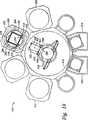
図3は、支持リング120の一実施の形態の上面図である。支持リング120は、ベース202に取付けられている4つの基板支持部材204a−dを含んでいる。ベース202は円形のリングであり、その中に中央開口206が限定されている。ベース202は、下側ペデスタル116上に取付けられるようになっている。ベース202は更に、ベース202の周縁に形成されている円周方向のシーリングリップ210を含み、基板支持部材100が上側処理位置に位置決めされた時、このシーリングリップ210は処理チャンバとの間にシールを形成する(図1参照)。シーリングリップ210と処理チャンバとの間に形成されるシールは、チャンバの下側部分と接触している基板支持部材の背後からガスが流出するのを阻止する。ベース上に配置されている基板支持部材204c、dは開口220を限定しており、この開口を通して基板ハンドラーブレードが運動し、基板の受渡しを実行することを可能にしている。基板支持具118は垂直に運動して基板支持部材204c、dと係合することができる。同様に、基板支持部材204c、dの反対側に配置されている基板支持部材204a、bは開口218を限定しており、この開口を通して基板ハンドラーブレード及び基板支持具118を伸ばすことができる。基板支持部材204aと204cとの間、及び204bと204dとの間に開口221a、bがそれぞれ設けられており、基板ハンドラーブレード及び基板支持具118の横方向ウィング(図8に図示してあり、後述する)を受入れてシステムの成分間の接触を最小にするようになっている(図12−17を参照して後述する)。支持リング120のベース202上に位置合わせタブ208が形成されており、基板支持部材100の位置合わせを支援する。システムの始動前の組立て中に、位置合わせタブ208は、上側支持リング120及び基板支持アセンブリ115がチャンバ160内に適切に位置決めされることを示す視覚支持を与える。
【0025】
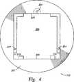
図4は、図3の支持リングの下面図である。開口206の周りのベース202内には複数のリフトピン凹み224が形成されており、リフトピン114を受入れるようになっている。リフトピン凹み224は、支持リング120の円周に沿って離間しており、支持リング120が上昇位置に持上がった時に、支持リング120のための安定な支持具を提供する。リフトピン114及びリフトピン凹み224は、支持リング112を下側ペデスタル116上に位置合わせするために使用することもできる。
【0026】
図5及び6はそれぞれ、図3の5−5矢視、及び6−6矢視断面図であって、支持リング120の基板支持部材204a−dを更に示している。基板支持部材204a−dはベース202上に取付けられ、開口206の周縁の周りに配置されている。基板支持部材204は、上側表面212、外側表面213、及び内側表面215を含む。内側表面215は、上側表面212から傾斜して配置されている上側基板位置合わせ表面214を含んでいる。上側基板位置合わせ表面214はその上に受入れた基板222を、重力の援助によって大よそ位置合わせする。基板位置合わせ表面214の下には垂直な基板捕捉表面217が設けられており、基板受入れ領域の外側境界を限定している。基板支持部材204の下側部分216は、約2°乃至約7°、好ましくは約2.5°乃至約5°の角度に配置されている傾斜した表面を有している。基板支持部材204a−dの下側部分216の傾斜は、基板222と基板支持部材204a−dとの間の接触面積Aを最小にする。傾斜した表面及び下側部分216は、基板をその上に受入れる時の基板の心合わせをも支援する。
【0027】
支持リング120は、掻き傷または変形のような破損を生ずることなく支持リング120をエッチングプロセス中に繰り返し使用できるように、一般的に酸化アルミニウムのような耐エッチング、耐高温材料で形成される。支持リング120は、アルミニウムペデスタル116と良好に適合するように、単片材料で形成することが好ましい。しかしながら、支持リング120は、複数の成分で作ることができる。
【0028】
図7は、下側ペデスタル116の断面図であって、ペデスタル116のボディ121の周縁に配置されている基板支持部材204a−d及び基板支持リッジ125を示している。基板支持リッジ125は、処理中に基板を支持する支持表面を限定している。基板222が基板支持リッジ125上に受入れられた時、下側ペデスタル116のボディ121と基板222の下面との間に空間170が限定される。処理中に、熱伝導を促進し且つプロセスガスが基板222の背後に導入されないようにするために、空間170内に背面ガスを流入させることができる。背面ガスは、例えば遠隔配置された背面ガス源190から陰極100の表面へのガス入口(図示してない)を通して、ペデスタル116内に配置されている背面ガスライン188によって空間170内へ供給することができる。
【0029】
熱を基板222から基板支持部材100へ効率的に伝達し、背面汚染を防ぐために、基板222の下に実質的なガス圧を存在させることができる。クランプリング(図示してない)を支持リング120の周縁に取付け、基板支持部材100と基板222との間に実質的な背面ガス圧が印加された時に基板支持部材100上に基板222を保持することができる。このようなクランプリングは、カリフォルニア州サンタクララのApplied Materials, Inc.製のP5000プラットフォームのM×Pチャンバにおける基板支持部材100上に基板を保持するために使用されるものと類似していよう。
【0030】
基板ハンドラーブレード
図8は、基板ハンドラーブレード300の概要上面図である。基板ハンドラーブレード300は、その両端に配置されている1対の基板支持具305、322を有するベース板302を含んでいる。1対の保持ウィング308が、ベース板302のベースにおいてベース板302に結合されており、それらの上に基板支持表面を限定している。保持ウィング308は、ウィングベース310、垂直支持具312、及びその上に基板320を保持して基板320の横方向運動を防ぐようになっている横方向肩部314を含む。保持ウィング308は、基板320を垂直及び水平の両方向に支持するものであれば、どのような形状にも構成することができる。図示のように、保持ウィングは、基板320を水平及び垂直に支持するように、“L字形”であることができる。先端の基板支持部材322はベース板302に結合され、垂直支持具326及び第2の肩部324を含む。垂直支持具326は、ベース板302と第2の肩部324との間が傾斜している。傾斜した表面はブレード300の中心に面しており(図11参照)、その上に支持する基板320の縁との接触を限定するようになっている。ベース板302は、基板をロードまたは処理チャンバ内から回収する、または処理チャンバ内へ配置する時に、ブレードを位置合わせするための複数の(好ましくは、2つの)位置合わせアパーチャ316をも含んでいる。
【0031】
図9及び10はそれぞれ、図8の基板ハンドラーブレード300の9−9矢視及び10−10矢視断面図である。肩部304(及び表面305)、314、324は、基板ハンドラーブレード300によって位置決めされる基板320(図示してない)のための領域を画定している。肩部304、314、324は、基板320がブレード300の縁を越えて運動しないようにしている。このような運動があると、基板320がブレード300の他の成分と接触して破損するか、または処理システム内における基板の位置合わせ及び支持が失われ得る。
【0032】
基板ハンドラーブレード300が基板320を回収する時、基板320は、保持ウィング308の垂直支持具312上と、保持指322の垂直支持具326上と、第1の肩部304の傾斜した支持表面305とに載っている。垂直支持具312、326、及び傾斜した表面305は、基板をブレード300上に位置合わせする。
【0033】
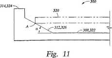
図11を参照する。傾斜表面付きの垂直支持具312、326を使用することによって、基板と基板ハンドラーブレードとの接触は垂直支持具312、326及び基板支持表面305上の勾配上の点Aに制限される。垂直支持具312、326、及び好ましくは傾斜した基板支持表面305は典型的に、ベース板302及びウィングベース310との間に小さい角度αを形成するように傾斜を付けてあり、基板320が垂直支持具312、326、及び傾斜した基板支持表面305上位置決めされた時に基板320とそれぞれの垂直支持具との間の接触面積を減少させるようになっている。垂直支持具312、326、及び傾斜した表面305の角度αは、好ましくは約2°乃至約7°であるが、異なる装置において異なる基板を使用する場合、及び異なる基板ハンドラーブレードを使用する場合には変化させることができる。
【0034】
ブレード上への基板の適切な位置合わせは、ブレードが、1つまたはそれ以上のロードロックプラットフォーム416を含むロードロック416(図18に示す)に進入する時に達成される。各ロードロックプラットフォームは、基板を支持した時に支持具と基板との間の接触を最小にし、しかも基板をクラスタツール(図示してない)の処理チャンバから回収したり、処理チャンバ内へ配置するためにブレードにアクセスできるように設計されている。ブレード300と基板320とを回収段階において適切に位置合わせすることにより、転送中の基板の運動が最小になり、また処理チャンバ412内へ配置する際の掻き傷及び誤位置合わせの機会を減少させる。位置合わせは、1つまたはそれ以上の(好ましくは、ブレード300に沿って横方向に配置されている2つの)位置合わせ開口316の使用によって支援される。整合する位置合わせ開口のセットが、ブレード300内に形成されている1つまたはそれ以上の位置合わせ開口と同じ形態で、ロードロックプラットフォームのベース内に配置されている。基板ハンドラーがロードロック416へ進入すると、ブレード300の位置合わせ開口316がロードロックプラットフォーム内の位置合わせ開口と一致し、それによって基板320が好ましい位置へ取付けられるようになる。
【0035】
保持ウィング308が存在することによってブレードのたわみの量が減少して運動許容度がより厳格になって、システム内における運動または配置中のブレードまたは基板が損損しなくなり、また基板取扱い中の基板ハンドラーブレード上での基板の運動が最小になる。ブレードのたわみとは、ブレードの剛さ、及び基板の取扱い中に経験するブレードの関連付けられた垂下のことである。
【0036】
例えば、基板をブレード上にロードする場合、基板の運動速度、基板の質量、基板ハンドラー/ブレード成分の摩耗、及びチャンバ温度に依存して、ブレードのたわみは変化し得る。保持ウィング308を使用して構造的支持を与えることによって、クロスブレードたわみ量、及び基板の運動を最小にすることができる。取扱い中の基板の誤位置合わせが、支持リング上の基板の誤位置合わせをもたらす可能性があり、それが基板内に欠陥が形成される可能性を増加させるので、たわみの量は臨界的であり得る。
【0037】
ブレード300上での基板の運動が減少すると、ブレード上での基板の運動による基板の掻き傷が形成されにくくなり、また基板の位置合わせも改善されるので、誤位置合わせによるエッチング、及び堆積、及び支持リング120からの基板の回収中の欠陥が少なくなる。更に、基板を輸送するために基板アダプタを確保する必要を排除したことによって、必要な処理ステップが少なくなり、使用される空間が小さくなる。これらは、従来技術によって達成できるよりも高い処理スループットに寄与することができる。
【0038】
ブレード300は、変化するチャンバ状態(圧力及び温度を含む)の下でブレードのたわみを減少させるような安定な、軽量材料で作ることが好ましい。本発明に有利に使用することができる1つの好ましい材料は、チタンである。他の有用な材料は、基板上に累積し得る静電荷の放電を促進する半導電性材料を含む。半導電性特性は、ブレードと他のシステム成分との間にアークをもたらす恐れがある高い導電性を好ましく回避する。しかしながら、チタンのような耐エッチング金属が最も好ましい。本発明の基板ハンドラーブレード300は、シングル基板ハンドラー、デュアル基板ハンドラー、デュアル独立基板ハンドラー、及びデュアルブレード基板ハンドラーで、及び好ましくはフォトマスクのエッチング処理において基板を転送するために基板ハンドラーブレードが使用されるような、種々の他の基板ハンドラ形態で使用することができる。
【0039】
図12は、基板転送中に、支持リング120上に配置された基板ハンドラーブレード300の上面図である。図では、基板222が傾斜した基板支持表面305、及びブレード300の垂直支持具312、326上に配置されている。ブレード300のベース板302は、ブレードのベースに配置された基板支持具204c、dの間に限定されている開口220を通して運動する。保持ウィング308は、支持リング120内の開口221a、bと整列し、これらの開口の中に位置している。ブレード300の先端は、基板支持具204a、bの先端間に限定された開口118内に位置している。この基板転送位置においては、ブレード300の傾斜した基板支持表面305及び垂直支持具312、326は、基板支持部材204の傾斜した下側部分216と整列している。開口218、220、及び221a、bは、ブレードが半径方向に運動する際に、または支持リング120が垂直に変位する際に、ベース板302、保持指322、及び保持ウィング308が支持リング120と接触しないようにする。
【0040】
図13−16は、ブレード300から支持リング120までの基板222の転送を示している。ブレード300は、ロードロックチャンバ(図示してない)から基板222を受け、基板222を処理チャンバ160(図1に示す)内へ送給する。次いで、ブレード300上に配置された基板222は、上述したように、そして図14に示してあるように、垂直に変位した位置にある支持リング120と水平方向に整列する。次に、図15に示すように、支持リング120はリフトピン114によって上方へ運動し、基板222と接触してそれをブレード300から持上げることができるようになる。基板支持具204a−dの下側部分216が、基板222を、第1の肩部の傾斜した基板支持表面305、及び保持ウィング308の垂直支持具312、326、及び指322から持上げる。図16に示すように、支持リング120は、ブレード300を支持リング120の上面202、または基板222の底面と接触させることなく、ブレード300を処理チャンバから引出すことを可能にするように十分に垂直に変位する。ブレードが引出された後に、図17に示すように、処理のためにリフトピンによって支持リング120が下側ペデスタル116の基板支持リッジ125上に下降させられる。
【0041】
処理済みの基板222を支持リング120から回収する場合には、支持リング120が、下側ペデスタル116の基板支持リッジ125から基板転送位置まで垂直に変位する。基板ハンドラーブレード300が処理チャンバ412内へ進入し、図14に示すように、ブレード300は基板222と支持リング120の上面202との間に整列する。ブレード300が支持リング120と整列すると、ブレード300の傾斜した基板支持表面305及び垂直支持具312、326は、基板支持部材204の傾斜した下側部分216の下の垂直に変位した位置に配置される。次いで、支持リング120が下降させられ、図13に示すように、傾斜した基板支持表面305及び垂直支持具312、326は、それらの上に基板222を支持するようになる。支持リング120は下側位置に垂直に変位し、図13に示すように、支持リング120と接触させることなくブレード300をチャンバ412から引出すことができるようになる。下側位置に達した支持リング120は、ブレード300から別の基板を受入れる準備が整う。基板ハンドラーブレードがチャンバ412から引出されて処理済みの基板をロードロックチャンバ416へ戻し、次いで別の基板222を探して処理チャンバ160内に配置する。
【0042】
以上に説明した支持装置及び基板ハンドラーブレード300は、基板を支持するようになっている基板処理システム410内に利用することもできる。基板処理システム410は、転送チャンバ414と、支持表面及び支持表面に結合されていて基板を受入れるようになっている支持リングを有する基板支持部材100を有する少なくとも1つの処理チャンバ412と、転送チャンバ414内に配置されている基板ハンドラー418とを含むことができる。基板ハンドラー418は、好ましくは、上述した基板ハンドラーブレード300を有している。処理チャンバは、好ましくは、プラズマエッチングチャンバである。
【0043】
図18は、上述した本発明の装置と共に使用するのに適する真空クラスタツール410の平面図である。真空クラスタツールは、転送チャンバのような中央真空チャンバ414上に取付けられている複数の基板処理チャンバ412を含み、1つまたはそれ以上のロードロックチャンバ416内に配置されている基板カセットから1つまたはそれ以上の処理チャンバ412へ基板を転送するようになっている。図18に示されているものと類似するクラスタツールは、カリフォルニア州サンタクララのApplied Materials, Inc.から入手可能なCenturaTM処理システムである。
【0044】
処理チャンバ412間の基板の転送は、典型的には、基板取扱いモジュール、または基板ハンドラー418(好ましくは、その上に取付けられている基板取扱いブレード300を有する)によって管理される。基板ハンドラー418は、中央転送チャンバ414内に配置されている。基板は処理された後に処理チャンバ412から回収され、ロードロックチャンバ416の1つまたはそれ以上へ、及び1つまたはそれ以上のロードロックチャンバ416内に配置されている1つまたはそれ以上の基板カセット(図示してない)内へ転送される。次いで、基板はロードロックチャンバ416から回収され、別の処理のために次のシステムへ転送することができる。フォトマスク製造処理においては、処理チャンバは、エッチングチャンバ、好ましくはプラズマエッチングチャンバである。
【0045】
以上に、本発明の好ましい実施の形態を説明したが、特許請求の範囲に記載されている本発明の範囲から逸脱することなく本発明の他の、及びさらなる実施の形態を考案することが可能である。
【図面の簡単な説明】
【図1】 本発明の支持リングを含むエッチングチャンバの概要図である。
【図2】 支持リングが取付けられている基板支持部材100の分解斜視図である。
【図3】 図3の支持リングの概要上面図である。
【図4】 本発明の支持リングの概要底面図である。
【図5】 図3の5−5矢視概要断面図である。
【図6】 図3の6−6矢視概要断面図である。
【図7】 下側ペデスタル及び上側支持リングの断面図である。
【図8】 本発明の基板ハンドラーの概要上面図である。
【図9】 図8の9−9矢視概要断面図である。
【図10】 図8の10−10矢視概要断面図である。
【図11】 ブレード300の垂直表面の概要断面図である。
【図12】 本発明の支持リングと共に本発明の基板ハンドラーを示す概要上面図である。
【図13】 本発明の支持リングに関係付けた本発明の基板ハンドラーの斜視図である。
【図14】 図12の斜視図である。
【図15】 本発明の支持リングに関係付けた本発明の基板ハンドラーの斜視図である。
【図16】 本発明の支持リング内の基板の斜視図である。
【図17】 本発明の支持リング内の基板の斜視図である。
【図18】 半導体基板のバッチ処理のための放射状クラスタツールの概要平面図である。[0001]
(Field of Invention)
The present invention relates generally to a method and apparatus for supporting and transferring a substrate during photomask fabrication.
[0002]
(Conventional technology)
Semiconductor device geometries have been dramatically reduced in size since these devices were first introduced several decades ago. Since then, integrated circuits have nearly followed the two-year / half-size rule (often referred to as Moore's law), which represents the number of devices on a chip doubling in two years. Today's manufacturing plants routinely produce 0.35 μm feature size devices, and even 0.18 μm feature size devices, and tomorrow's plant will soon produce devices with smaller geometries. Let's start manufacturing.
[0003]
As the perimeter of submicron technology has been squeezed, additional demands have been placed on the processes used to manufacture semiconductor devices to increase circuit density. For example, as circuit density increases, vias, contacts, and other features, as well as the width of the dielectric material between them, has decreased to sub-micron dimensions, but the thickness of the dielectric material remains substantially constant. As a result, the aspect ratio (ie, height / width) of the feature increases. Reliable formation of high aspect ratio features is important for the success of submicron technology and for the ongoing efforts to increase circuit density and individual substrate and die quality.
[0004]
Traditionally, high aspect ratio features have been formed by patterning the surface of a substrate to limit the dimensions of the features, and then etching the substrate to remove material and limiting the features. In order to form high aspect ratio features with the desired height to width ratio, the dimensions of the features need to be formed using some parameters, typically defined as the critical dimensions of these features. is there. In order to reliably form high aspect ratio features with the desired critical dimensions, precise patterning of the substrate followed by etching is required.
[0005]
Photolithography is one of the techniques used to form a precise pattern on a substrate. In conventional photolithographic processes, a photoresist is applied over one or more layers to be etched, and the photoresist is passed through a photolithographic substrate or photomask (which limits the desired form of the feature) to a pattern of light. To expose the features (eg, contacts, vias, or interconnects) to be etched in the layer. A light source that emits ultraviolet (UV) light can be used to expose the photoresist to chemically change the composition of the photoresist. The exposed or alternatively unexposed photoresist material is then removed to expose the underlying substrate material, leaving the photoresist material retained as an etch resistant pattern on the substrate. The exposed underlying material is then etched to form the desired features in the substrate.
[0006]
A photolithographic photomask or reticle typically consists of a substrate of an optically transparent silicon-based material, such as quartz, and light of a metal (typically chromium) that is patterned on the surface of the substrate. It has a shielding layer. The metal layer is patterned to form etched features. These features define the pattern and correspond to the dimensions of the features that are transferred to the substrate that is patterned by the photolithographic process.
[0007]
In order to deposit and etch a thin metal layer of a photomask, the substrate needs to be transferred and supported in the processing system. It would be desirable to use processing equipment and systems that are configured to process the substrate itself to produce a photomask. However, typically these systems are configured to process circular substrates and must be reconfigured to support and transfer a rectangular photomask. In addition, systems used to support and transfer substrates used in photomask manufacturing must handle the substrate carefully to prevent scratches and other defects from forming on the substrate. These defects can change the light transmission properties of the substrate, resulting in a photomask having defects.
[0008]
Accordingly, there is a need for a method and apparatus for transferring and supporting a substrate in a processing system so as to minimize the formation of defects.
[0009]
(Summary of Invention)
One aspect of the present invention provides an apparatus for supporting a substrate on a pedestal or cathode in a processing chamber so as to minimize contact between the substrate and chamber components during processing. Another aspect of the invention provides a substrate handler blade. The substrate handler minimizes contact between the substrate handler and the substrate during transfer of the substrate and supports the substrate to be held angularly and linearly on the blade.
[0010]
The present invention generally provides a substrate support member design in a plasma etch chamber and a substrate handler blade design that minimizes defects formed in the substrate during processing and handling of the substrate. One aspect of the present invention provides an apparatus for supporting a substrate, the apparatus comprising a support ring having one or more substrate support members mounted thereon, and one or more substrate support members. One or more openings extending through and adapted to receive the substrate. Preferably, the one or more substrate support members include an upper portion, a lower portion, and a tapered portion disposed between the upper portion and the lower portion, the lower portion having an inclined surface. is doing.
[0011]
An apparatus for supporting a substrate includes: an enclosure defining a processing region; a substrate support member having a support surface disposed within the enclosure; and a support ring coupled to the support surface to receive the substrate Can be used in a processing chamber containing
[0012]
Another aspect of the invention provides a substrate handler blade that includes a base plate and one or more retaining wings extending from the base plate. The one or more retaining wings include a base portion, a vertical support portion, and an end portion, preferably the vertical support portion includes an inwardly inclined surface.
[0013]
An apparatus for supporting a substrate is disposed in a transfer chamber, a substrate support member having a support surface, and at least one processing chamber having a support ring coupled to the support surface and adapted to receive the substrate, and the transfer chamber. It can also be used in a substrate processing system that includes a conventional substrate handler. Preferably, the substrate processing system further includes a substrate handler blade including a base plate and one or more holding wings connected to the substrate handler and extending from the base plate.
[0014]
In order to explain the above-mentioned features, advantages and objects of the present invention, and in order to understand the present invention in more detail, embodiments of the present invention will be described below with reference to the accompanying drawings. . However, it should be understood that the attached drawings are merely illustrative of exemplary embodiments of the invention and are not intended to limit the scope of the invention.
[0015]
(Embodiment)
FIG. 1 is a schematic cross-sectional view of one embodiment of a
[0016]
The process gas is introduced into the
[0017]
One chamber that can be advantageously used is a decoupled plasma source, or DPS, from Applied Materials, Inc., Santa Clara, California.TMInductively coupled plasma etching chamber. Other processing chambers are also suitable for use, including a deposition chamber as well as an etching chamber. These other types of chambers can include, for example, capacitively coupled parallel plate chambers and magnetically enhanced ion etching chambers.
[0018]
Generally speaking, the
[0019]
The
[0020]
FIG. 2 is an exploded perspective view of an embodiment of the
[0021]
The
[0022]
The
[0023]
The
[0024]
FIG. 3 is a top view of one embodiment of the
[0025]
FIG. 4 is a bottom view of the support ring of FIG. A plurality of lift pin recesses 224 are formed in the
[0026]
5 and 6 are sectional views taken along arrows 5-5 and 6-6 in FIG. 3, respectively, and further illustrate
[0027]
The
[0028]
FIG. 7 is a cross-sectional view of the
[0029]
In order to efficiently transfer heat from the
[0030]
PCB handler blade
FIG. 8 is a schematic top view of the
[0031]
9 and 10 are sectional views of the
[0032]
When the
[0033]
Please refer to FIG. By using
[0034]
Proper alignment of the substrate on the blade is achieved when the blade enters a load lock 416 (shown in FIG. 18) that includes one or more
[0035]
The presence of the holding
[0036]
For example, when loading a substrate onto a blade, the deflection of the blade may vary depending on the speed of movement of the substrate, the mass of the substrate, the wear of the substrate handler / blade component, and the chamber temperature. By using the retaining
[0037]
When the movement of the substrate on the
[0038]
[0039]
FIG. 12 is a top view of the
[0040]
FIGS. 13-16 illustrate the transfer of the
[0041]
When the processed
[0042]
The support apparatus and
[0043]
FIG. 18 is a plan view of a
[0044]
Transfer of substrates between the processing
[0045]
While preferred embodiments of the invention have been described above, other and further embodiments of the invention may be devised without departing from the scope of the invention as set forth in the claims. It is.
[Brief description of the drawings]
FIG. 1 is a schematic view of an etching chamber including a support ring of the present invention.
FIG. 2 is an exploded perspective view of a
3 is a schematic top view of the support ring of FIG. 3. FIG.
FIG. 4 is a schematic bottom view of the support ring of the present invention.
5 is a schematic cross-sectional view taken along arrow 5-5 in FIG. 3;
6 is a schematic sectional view taken along arrow 6-6 in FIG. 3;
FIG. 7 is a cross-sectional view of the lower pedestal and the upper support ring.
FIG. 8 is a schematic top view of the substrate handler of the present invention.
9 is a schematic cross-sectional view taken along line 9-9 in FIG.
10 is a schematic cross-sectional view taken along arrow 10-10 in FIG.
11 is a schematic cross-sectional view of a vertical surface of a
FIG. 12 is a schematic top view showing the substrate handler of the present invention together with the support ring of the present invention.
FIG. 13 is a perspective view of a substrate handler of the present invention associated with a support ring of the present invention.
FIG. 14 is a perspective view of FIG.
FIG. 15 is a perspective view of a substrate handler of the present invention associated with a support ring of the present invention.
FIG. 16 is a perspective view of a substrate in the support ring of the present invention.
FIG. 17 is a perspective view of a substrate in the support ring of the present invention.
FIG. 18 is a schematic plan view of a radial cluster tool for batch processing of semiconductor substrates.
Claims (12)
Translated fromJapanese処理領域を定める外囲と、
該外囲内に配置され、取り付け板の上に取り付けられた基板支持表面及び1又はそれ以上のペデスタル基板支持部材を有するペデスタルと、
内部に開口を定めるベースプレートであって、該開口が、前記基板支持表面と、当該ベースプレートに取り付けられ該開口の外周部分を形成する1又はそれ以上の基板支持部材と、を受け入れるように構成された、ベースプレートと、
を具備し、
前記1又はそれ以上の基板支持部材が、
基板を受け入れるように、かつ、
鉛直方向に移動して、前記ペデスタルの上に取り付けられた前記1又はそれ以上のペデスタル基板支持部材と係合する関係を形成することが可能となるように、
構成され、
前記基板がレティクルである、
ことを特徴とする処理チャンバ。A processing chamber,
An enclosure defining a processing area;
A pedestal havinga substrate support surface and one or more pedestal substrate support members disposed within the enclosure andmounted on amounting plate ;
A base plate defining an opening therein, the opening is, with the substrate support surface is configured to receive the one or more substrate support members to form a peripheral portion of themounting et Re opening in the base plate, the The base plate,
Comprising
The one or more substrate support members;
To accept the substrate, and
Inorder to be ableto move in a vertical directionand form a relationship to engage with the one or more pedestal substrate support membersmounted on the pedestal,
Configured,
The substrate is a reticle;
A processing chamber.
該1又はそれ以上の傾斜した支持表面が、前記基板を前記ベースプレートの中心部分に位置するように調節する、請求項1に記載の処理チャンバ。Further comprising one or more inclined support surfaces disposed on the base plate;
The processing chamber of claim 1, wherein the one or more inclined support surfaces adjust the substrate to be located in a central portion of the base plate.
内部に開口を定めており、ペデスタルの上に取り付けられ該ペデスタルから1又はそれ以上のリフトピンを受け入れるように構成された、ベースプレートと、
該ベースプレートに取り付けられ、前記開口の外周部分を形成する、1又はそれ以上の基板支持部材であって、上側部分と、下側部分と、前記ベースプレートの上に垂直に配置される基板を受け入れるために該上側部分と該下側部分との間に配置されたテーパー付き部分と、により構成される1又はそれ以上の基板支持部材と、
を具備し、
前記基板がレティクルである、ことを特徴とする装置。An apparatus for supporting a substrate,
Internal stipulates an opening in, configured to receive one or more lift pins from themounting et Re said pedestal on a pedestal, and a base plate,
Mounting et is in the base plate to form a peripheral portion of the opening, a one or more of the substrate support member receives the upper portion, a lower portion, a substrate disposed vertically on the base plate One or more substrate support members comprised of, for example, a tapered portion disposed between the upper portion and the lower portion;
Equippedwith,
The apparatus is characterizedin that thesubstrate is a reticle .
Applications Claiming Priority (5)
| Application Number | Priority Date | Filing Date | Title |
|---|---|---|---|
| US18831700P | 2000-03-10 | 2000-03-10 | |
| US60/188,317 | 2000-03-10 | ||
| US09/629,322US6537011B1 (en) | 2000-03-10 | 2000-07-31 | Method and apparatus for transferring and supporting a substrate |
| US09/629,322 | 2000-07-31 | ||
| PCT/US2001/007932WO2001069660A2 (en) | 2000-03-10 | 2001-03-12 | Method and apparatus for supporting a substrate |
Publications (2)
| Publication Number | Publication Date |
|---|---|
| JP2003536243A JP2003536243A (en) | 2003-12-02 |
| JP4869533B2true JP4869533B2 (en) | 2012-02-08 |
Family
ID=26883951
Family Applications (1)
| Application Number | Title | Priority Date | Filing Date |
|---|---|---|---|
| JP2001567027AExpired - Fee RelatedJP4869533B2 (en) | 2000-03-10 | 2001-03-12 | Apparatus for supporting process chamber and substrate |
Country Status (6)
| Country | Link |
|---|---|
| US (1) | US6537011B1 (en) |
| EP (1) | EP1261985A2 (en) |
| JP (1) | JP4869533B2 (en) |
| KR (1) | KR100775892B1 (en) |
| TW (1) | TW527628B (en) |
| WO (1) | WO2001069660A2 (en) |
Families Citing this family (39)
| Publication number | Priority date | Publication date | Assignee | Title |
|---|---|---|---|---|
| EP1217647B1 (en)* | 2000-12-21 | 2006-03-08 | Oxford Instruments Plasma Technology Limited | Substrate loading apparatus |
| US6935466B2 (en)* | 2001-03-01 | 2005-08-30 | Applied Materials, Inc. | Lift pin alignment and operation methods and apparatus |
| US20030168175A1 (en)* | 2002-03-08 | 2003-09-11 | Kim Kyung-Tae | Substrate alignment apparatus |
| US7048316B1 (en)* | 2002-07-12 | 2006-05-23 | Novellus Systems, Inc. | Compound angled pad end-effector |
| US7641247B2 (en)* | 2002-12-17 | 2010-01-05 | Applied Materials, Inc. | End effector assembly for supporting a substrate |
| DE10260645B3 (en)* | 2002-12-23 | 2004-09-16 | Infineon Technologies Ag | Compensation frame for holding substrate for semiconducting manufacture has polygonal inner profile for holding substrate, area of upper main surface of frame with different widths at different points |
| US7077973B2 (en)* | 2003-04-18 | 2006-07-18 | Applied Materials, Inc. | Methods for substrate orientation |
| US7128806B2 (en)* | 2003-10-21 | 2006-10-31 | Applied Materials, Inc. | Mask etch processing apparatus |
| US7319920B2 (en)* | 2003-11-10 | 2008-01-15 | Applied Materials, Inc. | Method and apparatus for self-calibration of a substrate handling robot |
| US20050133158A1 (en)* | 2003-12-19 | 2005-06-23 | Applied Materials, Inc. | Mask handler apparatus |
| JP2005209954A (en)* | 2004-01-23 | 2005-08-04 | Kawasaki Heavy Ind Ltd | Substrate holding device |
| JP2005340488A (en)* | 2004-05-27 | 2005-12-08 | Matsushita Electric Ind Co Ltd | Electronic device manufacturing equipment |
| US20080041716A1 (en)* | 2006-08-18 | 2008-02-21 | Schott Lithotec Usa Corporation | Methods for producing photomask blanks, cluster tool apparatus for producing photomask blanks and the resulting photomask blanks from such methods and apparatus |
| US20080099451A1 (en)* | 2006-10-30 | 2008-05-01 | Richard Lewington | Workpiece rotation apparatus for a plasma reactor system |
| US8920097B2 (en)* | 2006-11-02 | 2014-12-30 | Globalfoundries Singapore Pte. Ltd. | Wafer handling system for a loadlock |
| KR101397124B1 (en)* | 2007-02-28 | 2014-05-19 | 주성엔지니어링(주) | Substrate support frame, and substrate processing apparatus comprising the same, and method of loading and unloading substrate using the same |
| US8267636B2 (en) | 2007-05-08 | 2012-09-18 | Brooks Automation, Inc. | Substrate transport apparatus |
| TWI385812B (en)* | 2007-06-06 | 2013-02-11 | Motech Ind Inc | Supporting device, substrate transportation equipment and the method thereof |
| US9752615B2 (en) | 2007-06-27 | 2017-09-05 | Brooks Automation, Inc. | Reduced-complexity self-bearing brushless DC motor |
| JP5421255B2 (en) | 2007-06-27 | 2014-02-19 | ブルックス オートメーション インコーポレイテッド | Motor stator with lifting function and low cogging characteristics |
| US8283813B2 (en)* | 2007-06-27 | 2012-10-09 | Brooks Automation, Inc. | Robot drive with magnetic spindle bearings |
| CN101790673B (en)* | 2007-06-27 | 2013-08-28 | 布鲁克斯自动化公司 | Position feedback for self-bearing motors |
| US8823294B2 (en)* | 2007-06-27 | 2014-09-02 | Brooks Automation, Inc. | Commutation of an electromagnetic propulsion and guidance system |
| KR101660894B1 (en) | 2007-06-27 | 2016-10-10 | 브룩스 오토메이션 인코퍼레이티드 | Multiple dimension position sensor |
| KR101825595B1 (en) | 2007-07-17 | 2018-02-05 | 브룩스 오토메이션 인코퍼레이티드 | Substrate processing apparatus with motors integral to chamber walls |
| US20090182454A1 (en)* | 2008-01-14 | 2009-07-16 | Bernardo Donoso | Method and apparatus for self-calibration of a substrate handling robot |
| DE102008027861A1 (en)* | 2008-06-11 | 2009-12-17 | Vistec Semiconductor Systems Jena Gmbh | Device for holding disc-shaped objects |
| JP5885404B2 (en)* | 2010-08-04 | 2016-03-15 | 株式会社日立国際電気 | Substrate processing apparatus and semiconductor device manufacturing method |
| JP6099916B2 (en)* | 2012-09-25 | 2017-03-22 | 株式会社ダイヘン | Work transfer robot |
| ITCO20130073A1 (en)* | 2013-12-19 | 2015-06-20 | Lpe Spa | REACTION CHAMBER OF AN EPITAXIAL GROWTH REACTOR SUITABLE FOR USE WITH A LOADING / UNLOADING AND REACTOR DEVICE |
| EP3164884B1 (en) | 2014-07-03 | 2022-02-23 | LPE S.p.A. | Tool for manipulating substrates, manipulation method and epitaxial reactor |
| US9425076B2 (en)* | 2014-07-03 | 2016-08-23 | Applied Materials, Inc. | Substrate transfer robot end effector |
| WO2016111747A1 (en) | 2015-01-09 | 2016-07-14 | Applied Materials, Inc. | Substrate transfer mechanisms |
| US9564350B1 (en)* | 2015-09-18 | 2017-02-07 | Globalfoundries Inc. | Method and apparatus for storing and transporting semiconductor wafers in a vacuum pod |
| USD803283S1 (en)* | 2016-05-16 | 2017-11-21 | Veeco Instruments Inc. | Wafer handling assembly |
| US11075105B2 (en)* | 2017-09-21 | 2021-07-27 | Applied Materials, Inc. | In-situ apparatus for semiconductor process module |
| US11270898B2 (en)* | 2018-09-16 | 2022-03-08 | Applied Materials, Inc. | Apparatus for enhancing flow uniformity in a process chamber |
| DE102018007307A1 (en)* | 2018-09-17 | 2020-03-19 | Vat Holding Ag | Pen lifter |
| CN114914180A (en) | 2021-02-08 | 2022-08-16 | Asm Ip私人控股有限公司 | Wafer boat |
Family Cites Families (41)
| Publication number | Priority date | Publication date | Assignee | Title |
|---|---|---|---|---|
| US5374147A (en) | 1982-07-29 | 1994-12-20 | Tokyo Electron Limited | Transfer device for transferring a substrate |
| US4586743A (en) | 1984-09-24 | 1986-05-06 | Intelledex Incorporated | Robotic gripper for disk-shaped objects |
| US5280983A (en) | 1985-01-22 | 1994-01-25 | Applied Materials, Inc. | Semiconductor processing system with robotic autoloader and load lock |
| US4813732A (en) | 1985-03-07 | 1989-03-21 | Epsilon Technology, Inc. | Apparatus and method for automated wafer handling |
| JPS61273441A (en)* | 1985-05-23 | 1986-12-03 | Canon Inc | Wafer transfer device |
| US4705951A (en) | 1986-04-17 | 1987-11-10 | Varian Associates, Inc. | Wafer processing system |
| JPS637647A (en)* | 1986-06-28 | 1988-01-13 | Plasma Syst:Kk | Apparatus for processing semiconductor substrate |
| JPH0719150Y2 (en)* | 1986-10-31 | 1995-05-01 | 日本真空技術株式会社 | Wafer transfer hand |
| US4842683A (en)* | 1986-12-19 | 1989-06-27 | Applied Materials, Inc. | Magnetic field-enhanced plasma etch reactor |
| US5080549A (en) | 1987-05-11 | 1992-01-14 | Epsilon Technology, Inc. | Wafer handling system with Bernoulli pick-up |
| DE3803411A1 (en)* | 1988-02-05 | 1989-08-17 | Leybold Ag | DEVICE FOR HOLDING WORKPIECES |
| JPH01306583A (en)* | 1988-06-03 | 1989-12-11 | Japan Synthetic Rubber Co Ltd | Reactive ion etching device |
| US5022695A (en) | 1989-01-30 | 1991-06-11 | Texas Instruments Incorporated | Semiconductor slice holder |
| EP0600851B1 (en) | 1989-10-20 | 1999-02-03 | Applied Materials, Inc. | Robot apparatus |
| CH680275A5 (en) | 1990-03-05 | 1992-07-31 | Tet Techno Investment Trust | |
| US5180276A (en) | 1991-04-18 | 1993-01-19 | Brooks Automation, Inc. | Articulated arm transfer device |
| JPH05230673A (en)* | 1992-02-24 | 1993-09-07 | Ulvac Seimaku Kk | Dry etching device |
| US5580388A (en) | 1993-01-21 | 1996-12-03 | Moore Epitaxial, Inc. | Multi-layer susceptor for rapid thermal process reactors |
| US5352294A (en)* | 1993-01-28 | 1994-10-04 | White John M | Alignment of a shadow frame and large flat substrates on a support |
| CN1046654C (en) | 1993-04-16 | 1999-11-24 | 布鲁克斯自动化公司 | Articulated arm transfer device |
| US5643366A (en)* | 1994-01-31 | 1997-07-01 | Applied Materials, Inc. | Wafer handling within a vacuum chamber using vacuum |
| US5791895A (en)* | 1994-02-17 | 1998-08-11 | Novellus Systems, Inc. | Apparatus for thermal treatment of thin film wafer |
| JPH07297255A (en)* | 1994-04-26 | 1995-11-10 | Dainippon Screen Mfg Co Ltd | Holding device of board |
| JPH08309681A (en)* | 1995-05-17 | 1996-11-26 | Ulvac Japan Ltd | Multiarticulated substrate conveying robot |
| JP2676334B2 (en) | 1995-07-31 | 1997-11-12 | 住友重機械工業株式会社 | Robot arm |
| US5733096A (en) | 1995-09-13 | 1998-03-31 | Silicon Valley Group, Inc. | Multi-stage telescoping structure |
| US5669644A (en)* | 1995-11-13 | 1997-09-23 | Kokusai Electric Co., Ltd. | Wafer transfer plate |
| US5647626A (en) | 1995-12-04 | 1997-07-15 | Taiwan Semiconductor Manufacturing Company, Ltd. | Wafer pickup system |
| JPH09205130A (en)* | 1996-01-17 | 1997-08-05 | Applied Materials Inc | Wafer support device |
| US6102164A (en) | 1996-02-28 | 2000-08-15 | Applied Materials, Inc. | Multiple independent robot assembly and apparatus for processing and transferring semiconductor wafers |
| US6217663B1 (en)* | 1996-06-21 | 2001-04-17 | Kokusai Electric Co., Ltd. | Substrate processing apparatus and substrate processing method |
| JPH1074814A (en) | 1996-08-29 | 1998-03-17 | Kokusai Electric Co Ltd | Wafer transfer method and semiconductor manufacturing apparatus |
| US6395363B1 (en) | 1996-11-05 | 2002-05-28 | Applied Materials, Inc. | Sloped substrate support |
| US5955858A (en)* | 1997-02-14 | 1999-09-21 | Applied Materials, Inc. | Mechanically clamping robot wrist |
| JPH118291A (en) | 1997-06-18 | 1999-01-12 | Hitachi Ltd | Electrostatic suction device |
| JPH1126550A (en)* | 1997-07-04 | 1999-01-29 | Tokyo Electron Ltd | Substrate conveyer and apparatus for treating substrate, using the same |
| EP1036406B1 (en) | 1997-11-03 | 2003-04-02 | ASM America, Inc. | Improved low mass wafer support system |
| JPH11195695A (en)* | 1997-12-26 | 1999-07-21 | Advanced Display Inc | Electronic device manufacturing apparatus |
| US6203617B1 (en)* | 1998-03-26 | 2001-03-20 | Tokyo Electron Limited | Conveying unit and substrate processing unit |
| JP2000003951A (en)* | 1998-06-16 | 2000-01-07 | Tokyo Electron Ltd | Transfer device |
| JP2000049207A (en)* | 1998-07-28 | 2000-02-18 | Matsushita Electric Ind Co Ltd | Plasma processing method and apparatus |
- 2000
- 2000-07-31USUS09/629,322patent/US6537011B1/ennot_activeExpired - Fee Related
- 2001
- 2001-03-12TWTW090105749Apatent/TW527628B/enactive
- 2001-03-12WOPCT/US2001/007932patent/WO2001069660A2/ennot_activeApplication Discontinuation
- 2001-03-12EPEP01914803Apatent/EP1261985A2/ennot_activeWithdrawn
- 2001-03-12JPJP2001567027Apatent/JP4869533B2/ennot_activeExpired - Fee Related
- 2001-03-12KRKR1020027011881Apatent/KR100775892B1/ennot_activeExpired - Fee Related
Also Published As
| Publication number | Publication date |
|---|---|
| WO2001069660A2 (en) | 2001-09-20 |
| US6537011B1 (en) | 2003-03-25 |
| WO2001069660A3 (en) | 2002-04-25 |
| KR20020077937A (en) | 2002-10-14 |
| KR100775892B1 (en) | 2007-11-13 |
| JP2003536243A (en) | 2003-12-02 |
| EP1261985A2 (en) | 2002-12-04 |
| TW527628B (en) | 2003-04-11 |
Similar Documents
| Publication | Publication Date | Title |
|---|---|---|
| JP4869533B2 (en) | Apparatus for supporting process chamber and substrate | |
| US7879151B2 (en) | Mask etch processing apparatus | |
| US4988533A (en) | Method for deposition of silicon oxide on a wafer | |
| US4949671A (en) | Processing apparatus and method | |
| US4911103A (en) | Processing apparatus and method | |
| US4872938A (en) | Processing apparatus | |
| US4836905A (en) | Processing apparatus | |
| US4816098A (en) | Apparatus for transferring workpieces | |
| US4818327A (en) | Wafer processing apparatus | |
| US4904621A (en) | Remote plasma generation process using a two-stage showerhead | |
| US5248636A (en) | Processing method using both a remotely generated plasma and an in-situ plasma with UV irradiation | |
| US4875989A (en) | Wafer processing apparatus | |
| US4877757A (en) | Method of sequential cleaning and passivating a GaAs substrate using remote oxygen plasma | |
| US5138973A (en) | Wafer processing apparatus having independently controllable energy sources | |
| US4820377A (en) | Method for cleanup processing chamber and vacuum process module | |
| US4838990A (en) | Method for plasma etching tungsten | |
| US4910043A (en) | Processing apparatus and method | |
| US4837113A (en) | Method for depositing compound from group II-VI | |
| US4891488A (en) | Processing apparatus and method | |
| US4849067A (en) | Method for etching tungsten | |
| US4832777A (en) | Processing apparatus and method | |
| US4906328A (en) | Method for wafer treating | |
| US4830700A (en) | Processing apparatus and method | |
| US4874723A (en) | Selective etching of tungsten by remote and in situ plasma generation | |
| US4915777A (en) | Method for etching tungsten |
Legal Events
| Date | Code | Title | Description |
|---|---|---|---|
| A621 | Written request for application examination | Free format text:JAPANESE INTERMEDIATE CODE: A621 Effective date:20080305 | |
| A977 | Report on retrieval | Free format text:JAPANESE INTERMEDIATE CODE: A971007 Effective date:20110113 | |
| A131 | Notification of reasons for refusal | Free format text:JAPANESE INTERMEDIATE CODE: A131 Effective date:20110120 | |
| A521 | Request for written amendment filed | Free format text:JAPANESE INTERMEDIATE CODE: A523 Effective date:20110408 | |
| A131 | Notification of reasons for refusal | Free format text:JAPANESE INTERMEDIATE CODE: A131 Effective date:20110609 | |
| A521 | Request for written amendment filed | Free format text:JAPANESE INTERMEDIATE CODE: A523 Effective date:20110901 | |
| TRDD | Decision of grant or rejection written | ||
| A01 | Written decision to grant a patent or to grant a registration (utility model) | Free format text:JAPANESE INTERMEDIATE CODE: A01 Effective date:20111020 | |
| A01 | Written decision to grant a patent or to grant a registration (utility model) | Free format text:JAPANESE INTERMEDIATE CODE: A01 | |
| A61 | First payment of annual fees (during grant procedure) | Free format text:JAPANESE INTERMEDIATE CODE: A61 Effective date:20111116 | |
| R150 | Certificate of patent or registration of utility model | Free format text:JAPANESE INTERMEDIATE CODE: R150 | |
| FPAY | Renewal fee payment (event date is renewal date of database) | Free format text:PAYMENT UNTIL: 20141125 Year of fee payment:3 | |
| LAPS | Cancellation because of no payment of annual fees |