JP4862848B2 - Manufacturing method of semiconductor package - Google Patents
Manufacturing method of semiconductor packageDownload PDFInfo
- Publication number
- JP4862848B2 JP4862848B2JP2008067673AJP2008067673AJP4862848B2JP 4862848 B2JP4862848 B2JP 4862848B2JP 2008067673 AJP2008067673 AJP 2008067673AJP 2008067673 AJP2008067673 AJP 2008067673AJP 4862848 B2JP4862848 B2JP 4862848B2
- Authority
- JP
- Japan
- Prior art keywords
- wiring
- semiconductor
- copper foil
- nickel
- pattern
- Prior art date
- Legal status (The legal status is an assumption and is not a legal conclusion. Google has not performed a legal analysis and makes no representation as to the accuracy of the status listed.)
- Expired - Fee Related
Links
- 239000004065semiconductorSubstances0.000titleclaimsabstractdescription220
- 238000004519manufacturing processMethods0.000titleclaimsdescription50
- 238000007789sealingMethods0.000claimsabstractdescription44
- 238000000034methodMethods0.000claimsdescription113
- 238000007747platingMethods0.000claimsdescription74
- 238000005530etchingMethods0.000claimsdescription39
- PCHJSUWPFVWCPO-UHFFFAOYSA-NgoldChemical compound[Au]PCHJSUWPFVWCPO-UHFFFAOYSA-N0.000claimsdescription33
- 229920005989resinPolymers0.000claimsdescription32
- 239000011347resinSubstances0.000claimsdescription32
- 229910052737goldInorganic materials0.000claimsdescription30
- 239000010931goldSubstances0.000claimsdescription30
- 238000005520cutting processMethods0.000claimsdescription4
- RYGMFSIKBFXOCR-UHFFFAOYSA-NCopperChemical compound[Cu]RYGMFSIKBFXOCR-UHFFFAOYSA-N0.000abstractdescription151
- PXHVJJICTQNCMI-UHFFFAOYSA-NNickelChemical compound[Ni]PXHVJJICTQNCMI-UHFFFAOYSA-N0.000abstractdescription142
- 239000011889copper foilSubstances0.000abstractdescription106
- 229910052759nickelInorganic materials0.000abstractdescription70
- 229910000679solderInorganic materials0.000abstractdescription67
- 239000000758substrateSubstances0.000abstractdescription50
- 239000003822epoxy resinSubstances0.000abstractdescription26
- 229920000647polyepoxidePolymers0.000abstractdescription26
- 239000003513alkaliSubstances0.000abstractdescription10
- 230000010354integrationEffects0.000abstractdescription4
- 239000010410layerSubstances0.000description79
- 229920001721polyimidePolymers0.000description59
- 239000000463materialSubstances0.000description46
- 229910052751metalInorganic materials0.000description46
- 239000002184metalSubstances0.000description46
- 229910052802copperInorganic materials0.000description45
- 239000010949copperSubstances0.000description45
- 230000008569processEffects0.000description34
- 239000004642PolyimideSubstances0.000description33
- 239000010408filmSubstances0.000description33
- 239000002585baseSubstances0.000description32
- 239000011888foilSubstances0.000description30
- 238000012546transferMethods0.000description23
- 239000000853adhesiveSubstances0.000description17
- 230000001070adhesive effectEffects0.000description17
- 238000012545processingMethods0.000description13
- 229910000365copper sulfateInorganic materials0.000description12
- ARUVKPQLZAKDPS-UHFFFAOYSA-Lcopper(II) sulfateChemical compound[Cu+2].[O-][S+2]([O-])([O-])[O-]ARUVKPQLZAKDPS-UHFFFAOYSA-L0.000description12
- BQCADISMDOOEFD-UHFFFAOYSA-NSilverChemical compound[Ag]BQCADISMDOOEFD-UHFFFAOYSA-N0.000description11
- 238000009713electroplatingMethods0.000description11
- 239000007788liquidSubstances0.000description11
- 239000003566sealing materialSubstances0.000description11
- 229910052709silverInorganic materials0.000description11
- 239000004332silverSubstances0.000description11
- 238000011161developmentMethods0.000description10
- 239000010935stainless steelSubstances0.000description10
- 229910001220stainless steelInorganic materials0.000description10
- VYPSYNLAJGMNEJ-UHFFFAOYSA-NSilicium dioxideChemical compoundO=[Si]=OVYPSYNLAJGMNEJ-UHFFFAOYSA-N0.000description8
- 238000010438heat treatmentMethods0.000description7
- 238000004080punchingMethods0.000description7
- CURLTUGMZLYLDI-UHFFFAOYSA-NCarbon dioxideChemical compoundO=C=OCURLTUGMZLYLDI-UHFFFAOYSA-N0.000description6
- 238000007639printingMethods0.000description6
- KWYUFKZDYYNOTN-UHFFFAOYSA-MPotassium hydroxideChemical compound[OH-].[K+]KWYUFKZDYYNOTN-UHFFFAOYSA-M0.000description5
- 238000003825pressingMethods0.000description5
- 239000007921spraySubstances0.000description5
- 239000002313adhesive filmSubstances0.000description4
- 238000005516engineering processMethods0.000description4
- 230000009477glass transitionEffects0.000description4
- 239000000377silicon dioxideSubstances0.000description4
- 239000000126substanceSubstances0.000description4
- 238000001721transfer mouldingMethods0.000description4
- 229910000881Cu alloyInorganic materials0.000description3
- 239000001569carbon dioxideSubstances0.000description3
- 229910002092carbon dioxideInorganic materials0.000description3
- 238000003486chemical etchingMethods0.000description3
- 238000005538encapsulationMethods0.000description3
- 238000009413insulationMethods0.000description3
- 230000000149penetrating effectEffects0.000description3
- 230000009467reductionEffects0.000description3
- 229910021578Iron(III) chlorideInorganic materials0.000description2
- 229920001646UPILEXPolymers0.000description2
- 230000004888barrier functionEffects0.000description2
- 239000000919ceramicSubstances0.000description2
- 239000002131composite materialSubstances0.000description2
- 238000001816coolingMethods0.000description2
- 230000002950deficientEffects0.000description2
- 238000004090dissolutionMethods0.000description2
- 238000005553drillingMethods0.000description2
- 230000000694effectsEffects0.000description2
- RBTARNINKXHZNM-UHFFFAOYSA-Kiron trichlorideChemical compoundCl[Fe](Cl)ClRBTARNINKXHZNM-UHFFFAOYSA-K0.000description2
- 230000010355oscillationEffects0.000description2
- OFNHPGDEEMZPFG-UHFFFAOYSA-NphosphanylidynenickelChemical compound[P].[Ni]OFNHPGDEEMZPFG-UHFFFAOYSA-N0.000description2
- 238000007650screen-printingMethods0.000description2
- 238000001039wet etchingMethods0.000description2
- 229910000906BronzeInorganic materials0.000description1
- 229910000990Ni alloyInorganic materials0.000description1
- OAICVXFJPJFONN-UHFFFAOYSA-NPhosphorusChemical compound[P]OAICVXFJPJFONN-UHFFFAOYSA-N0.000description1
- 239000012790adhesive layerSubstances0.000description1
- 239000004840adhesive resinSubstances0.000description1
- 229920006223adhesive resinPolymers0.000description1
- 230000015572biosynthetic processEffects0.000description1
- 239000010974bronzeSubstances0.000description1
- 239000003795chemical substances by applicationSubstances0.000description1
- 239000011248coating agentSubstances0.000description1
- 238000000576coating methodMethods0.000description1
- 239000000470constituentSubstances0.000description1
- KUNSUQLRTQLHQQ-UHFFFAOYSA-Ncopper tinChemical compound[Cu].[Sn]KUNSUQLRTQLHQQ-UHFFFAOYSA-N0.000description1
- 230000007797corrosionEffects0.000description1
- 238000005260corrosionMethods0.000description1
- 229910003460diamondInorganic materials0.000description1
- 239000010432diamondSubstances0.000description1
- 229920006332epoxy adhesivePolymers0.000description1
- 230000005496eutecticsEffects0.000description1
- 239000011521glassSubstances0.000description1
- UCHOFYCGAZVYGZ-UHFFFAOYSA-Ngold leadChemical compound[Au].[Pb]UCHOFYCGAZVYGZ-UHFFFAOYSA-N0.000description1
- MSNOMDLPLDYDME-UHFFFAOYSA-Ngold nickelChemical compound[Ni].[Au]MSNOMDLPLDYDME-UHFFFAOYSA-N0.000description1
- 238000003780insertionMethods0.000description1
- 230000037431insertionEffects0.000description1
- 238000003475laminationMethods0.000description1
- 239000004850liquid epoxy resins (LERs)Substances0.000description1
- 150000002739metalsChemical class0.000description1
- 230000003647oxidationEffects0.000description1
- 238000007254oxidation reactionMethods0.000description1
- 238000004806packaging method and processMethods0.000description1
- 230000002093peripheral effectEffects0.000description1
- 238000001259photo etchingMethods0.000description1
- 229920002120photoresistant polymerPolymers0.000description1
- 239000004033plasticSubstances0.000description1
- 229920005575poly(amic acid)Polymers0.000description1
- 239000002243precursorSubstances0.000description1
- 239000002356single layerSubstances0.000description1
- 238000004381surface treatmentMethods0.000description1
- 230000008646thermal stressEffects0.000description1
- 229920001187thermosetting polymerPolymers0.000description1
- 239000010409thin filmSubstances0.000description1
Images


Classifications
- H—ELECTRICITY
- H01—ELECTRIC ELEMENTS
- H01L—SEMICONDUCTOR DEVICES NOT COVERED BY CLASS H10
- H01L21/00—Processes or apparatus adapted for the manufacture or treatment of semiconductor or solid state devices or of parts thereof
- H01L21/02—Manufacture or treatment of semiconductor devices or of parts thereof
- H01L21/04—Manufacture or treatment of semiconductor devices or of parts thereof the devices having potential barriers, e.g. a PN junction, depletion layer or carrier concentration layer
- H01L21/50—Assembly of semiconductor devices using processes or apparatus not provided for in a single one of the groups H01L21/18 - H01L21/326 or H10D48/04 - H10D48/07 e.g. sealing of a cap to a base of a container
- H01L21/56—Encapsulations, e.g. encapsulation layers, coatings
- H01L21/568—Temporary substrate used as encapsulation process aid
- H—ELECTRICITY
- H01—ELECTRIC ELEMENTS
- H01L—SEMICONDUCTOR DEVICES NOT COVERED BY CLASS H10
- H01L23/00—Details of semiconductor or other solid state devices
- H01L23/12—Mountings, e.g. non-detachable insulating substrates
- H—ELECTRICITY
- H01—ELECTRIC ELEMENTS
- H01L—SEMICONDUCTOR DEVICES NOT COVERED BY CLASS H10
- H01L21/00—Processes or apparatus adapted for the manufacture or treatment of semiconductor or solid state devices or of parts thereof
- H01L21/02—Manufacture or treatment of semiconductor devices or of parts thereof
- H01L21/04—Manufacture or treatment of semiconductor devices or of parts thereof the devices having potential barriers, e.g. a PN junction, depletion layer or carrier concentration layer
- H01L21/48—Manufacture or treatment of parts, e.g. containers, prior to assembly of the devices, using processes not provided for in a single one of the groups H01L21/18 - H01L21/326 or H10D48/04 - H10D48/07
- H01L21/4803—Insulating or insulated parts, e.g. mountings, containers, diamond heatsinks
- H—ELECTRICITY
- H01—ELECTRIC ELEMENTS
- H01L—SEMICONDUCTOR DEVICES NOT COVERED BY CLASS H10
- H01L21/00—Processes or apparatus adapted for the manufacture or treatment of semiconductor or solid state devices or of parts thereof
- H01L21/02—Manufacture or treatment of semiconductor devices or of parts thereof
- H01L21/04—Manufacture or treatment of semiconductor devices or of parts thereof the devices having potential barriers, e.g. a PN junction, depletion layer or carrier concentration layer
- H01L21/50—Assembly of semiconductor devices using processes or apparatus not provided for in a single one of the groups H01L21/18 - H01L21/326 or H10D48/04 - H10D48/07 e.g. sealing of a cap to a base of a container
- H01L21/56—Encapsulations, e.g. encapsulation layers, coatings
- H01L21/561—Batch processing
- H—ELECTRICITY
- H01—ELECTRIC ELEMENTS
- H01L—SEMICONDUCTOR DEVICES NOT COVERED BY CLASS H10
- H01L23/00—Details of semiconductor or other solid state devices
- H01L23/28—Encapsulations, e.g. encapsulating layers, coatings, e.g. for protection
- H01L23/31—Encapsulations, e.g. encapsulating layers, coatings, e.g. for protection characterised by the arrangement or shape
- H01L23/3107—Encapsulations, e.g. encapsulating layers, coatings, e.g. for protection characterised by the arrangement or shape the device being completely enclosed
- H01L23/3121—Encapsulations, e.g. encapsulating layers, coatings, e.g. for protection characterised by the arrangement or shape the device being completely enclosed a substrate forming part of the encapsulation
- H01L23/3128—Encapsulations, e.g. encapsulating layers, coatings, e.g. for protection characterised by the arrangement or shape the device being completely enclosed a substrate forming part of the encapsulation the substrate having spherical bumps for external connection
- H—ELECTRICITY
- H01—ELECTRIC ELEMENTS
- H01L—SEMICONDUCTOR DEVICES NOT COVERED BY CLASS H10
- H01L23/00—Details of semiconductor or other solid state devices
- H01L23/48—Arrangements for conducting electric current to or from the solid state body in operation, e.g. leads, terminal arrangements ; Selection of materials therefor
- H01L23/488—Arrangements for conducting electric current to or from the solid state body in operation, e.g. leads, terminal arrangements ; Selection of materials therefor consisting of soldered or bonded constructions
- H01L23/498—Leads, i.e. metallisations or lead-frames on insulating substrates, e.g. chip carriers
- H01L23/49811—Additional leads joined to the metallisation on the insulating substrate, e.g. pins, bumps, wires, flat leads
- H01L23/49816—Spherical bumps on the substrate for external connection, e.g. ball grid arrays [BGA]
- H—ELECTRICITY
- H01—ELECTRIC ELEMENTS
- H01L—SEMICONDUCTOR DEVICES NOT COVERED BY CLASS H10
- H01L23/00—Details of semiconductor or other solid state devices
- H01L23/48—Arrangements for conducting electric current to or from the solid state body in operation, e.g. leads, terminal arrangements ; Selection of materials therefor
- H01L23/488—Arrangements for conducting electric current to or from the solid state body in operation, e.g. leads, terminal arrangements ; Selection of materials therefor consisting of soldered or bonded constructions
- H01L23/498—Leads, i.e. metallisations or lead-frames on insulating substrates, e.g. chip carriers
- H01L23/4985—Flexible insulating substrates
- H—ELECTRICITY
- H01—ELECTRIC ELEMENTS
- H01L—SEMICONDUCTOR DEVICES NOT COVERED BY CLASS H10
- H01L24/00—Arrangements for connecting or disconnecting semiconductor or solid-state bodies; Methods or apparatus related thereto
- H01L24/01—Means for bonding being attached to, or being formed on, the surface to be connected, e.g. chip-to-package, die-attach, "first-level" interconnects; Manufacturing methods related thereto
- H01L24/26—Layer connectors, e.g. plate connectors, solder or adhesive layers; Manufacturing methods related thereto
- H01L24/31—Structure, shape, material or disposition of the layer connectors after the connecting process
- H01L24/32—Structure, shape, material or disposition of the layer connectors after the connecting process of an individual layer connector
- H—ELECTRICITY
- H01—ELECTRIC ELEMENTS
- H01L—SEMICONDUCTOR DEVICES NOT COVERED BY CLASS H10
- H01L24/00—Arrangements for connecting or disconnecting semiconductor or solid-state bodies; Methods or apparatus related thereto
- H01L24/80—Methods for connecting semiconductor or other solid state bodies using means for bonding being attached to, or being formed on, the surface to be connected
- H01L24/83—Methods for connecting semiconductor or other solid state bodies using means for bonding being attached to, or being formed on, the surface to be connected using a layer connector
- H—ELECTRICITY
- H01—ELECTRIC ELEMENTS
- H01L—SEMICONDUCTOR DEVICES NOT COVERED BY CLASS H10
- H01L24/00—Arrangements for connecting or disconnecting semiconductor or solid-state bodies; Methods or apparatus related thereto
- H01L24/93—Batch processes
- H01L24/95—Batch processes at chip-level, i.e. with connecting carried out on a plurality of singulated devices, i.e. on diced chips
- H01L24/97—Batch processes at chip-level, i.e. with connecting carried out on a plurality of singulated devices, i.e. on diced chips the devices being connected to a common substrate, e.g. interposer, said common substrate being separable into individual assemblies after connecting
- H—ELECTRICITY
- H05—ELECTRIC TECHNIQUES NOT OTHERWISE PROVIDED FOR
- H05K—PRINTED CIRCUITS; CASINGS OR CONSTRUCTIONAL DETAILS OF ELECTRIC APPARATUS; MANUFACTURE OF ASSEMBLAGES OF ELECTRICAL COMPONENTS
- H05K3/00—Apparatus or processes for manufacturing printed circuits
- H05K3/30—Assembling printed circuits with electric components, e.g. with resistor
- H—ELECTRICITY
- H01—ELECTRIC ELEMENTS
- H01L—SEMICONDUCTOR DEVICES NOT COVERED BY CLASS H10
- H01L2221/00—Processes or apparatus adapted for the manufacture or treatment of semiconductor or solid state devices or of parts thereof covered by H01L21/00
- H01L2221/67—Apparatus for handling semiconductor or electric solid state devices during manufacture or treatment thereof; Apparatus for handling wafers during manufacture or treatment of semiconductor or electric solid state devices or components; Apparatus not specifically provided for elsewhere
- H01L2221/683—Apparatus for handling semiconductor or electric solid state devices during manufacture or treatment thereof; Apparatus for handling wafers during manufacture or treatment of semiconductor or electric solid state devices or components; Apparatus not specifically provided for elsewhere for supporting or gripping
- H01L2221/68304—Apparatus for handling semiconductor or electric solid state devices during manufacture or treatment thereof; Apparatus for handling wafers during manufacture or treatment of semiconductor or electric solid state devices or components; Apparatus not specifically provided for elsewhere for supporting or gripping using temporarily an auxiliary support
- H01L2221/68377—Apparatus for handling semiconductor or electric solid state devices during manufacture or treatment thereof; Apparatus for handling wafers during manufacture or treatment of semiconductor or electric solid state devices or components; Apparatus not specifically provided for elsewhere for supporting or gripping using temporarily an auxiliary support with parts of the auxiliary support remaining in the finished device
- H—ELECTRICITY
- H01—ELECTRIC ELEMENTS
- H01L—SEMICONDUCTOR DEVICES NOT COVERED BY CLASS H10
- H01L2224/00—Indexing scheme for arrangements for connecting or disconnecting semiconductor or solid-state bodies and methods related thereto as covered by H01L24/00
- H01L2224/01—Means for bonding being attached to, or being formed on, the surface to be connected, e.g. chip-to-package, die-attach, "first-level" interconnects; Manufacturing methods related thereto
- H01L2224/10—Bump connectors; Manufacturing methods related thereto
- H01L2224/15—Structure, shape, material or disposition of the bump connectors after the connecting process
- H01L2224/16—Structure, shape, material or disposition of the bump connectors after the connecting process of an individual bump connector
- H01L2224/161—Disposition
- H01L2224/16151—Disposition the bump connector connecting between a semiconductor or solid-state body and an item not being a semiconductor or solid-state body, e.g. chip-to-substrate, chip-to-passive
- H01L2224/16221—Disposition the bump connector connecting between a semiconductor or solid-state body and an item not being a semiconductor or solid-state body, e.g. chip-to-substrate, chip-to-passive the body and the item being stacked
- H01L2224/16225—Disposition the bump connector connecting between a semiconductor or solid-state body and an item not being a semiconductor or solid-state body, e.g. chip-to-substrate, chip-to-passive the body and the item being stacked the item being non-metallic, e.g. insulating substrate with or without metallisation
- H01L2224/16237—Disposition the bump connector connecting between a semiconductor or solid-state body and an item not being a semiconductor or solid-state body, e.g. chip-to-substrate, chip-to-passive the body and the item being stacked the item being non-metallic, e.g. insulating substrate with or without metallisation the bump connector connecting to a bonding area disposed in a recess of the surface of the item
- H—ELECTRICITY
- H01—ELECTRIC ELEMENTS
- H01L—SEMICONDUCTOR DEVICES NOT COVERED BY CLASS H10
- H01L2224/00—Indexing scheme for arrangements for connecting or disconnecting semiconductor or solid-state bodies and methods related thereto as covered by H01L24/00
- H01L2224/01—Means for bonding being attached to, or being formed on, the surface to be connected, e.g. chip-to-package, die-attach, "first-level" interconnects; Manufacturing methods related thereto
- H01L2224/26—Layer connectors, e.g. plate connectors, solder or adhesive layers; Manufacturing methods related thereto
- H01L2224/28—Structure, shape, material or disposition of the layer connectors prior to the connecting process
- H01L2224/29—Structure, shape, material or disposition of the layer connectors prior to the connecting process of an individual layer connector
- H01L2224/29001—Core members of the layer connector
- H01L2224/29099—Material
- H01L2224/2919—Material with a principal constituent of the material being a polymer, e.g. polyester, phenolic based polymer, epoxy
- H—ELECTRICITY
- H01—ELECTRIC ELEMENTS
- H01L—SEMICONDUCTOR DEVICES NOT COVERED BY CLASS H10
- H01L2224/00—Indexing scheme for arrangements for connecting or disconnecting semiconductor or solid-state bodies and methods related thereto as covered by H01L24/00
- H01L2224/01—Means for bonding being attached to, or being formed on, the surface to be connected, e.g. chip-to-package, die-attach, "first-level" interconnects; Manufacturing methods related thereto
- H01L2224/26—Layer connectors, e.g. plate connectors, solder or adhesive layers; Manufacturing methods related thereto
- H01L2224/28—Structure, shape, material or disposition of the layer connectors prior to the connecting process
- H01L2224/29—Structure, shape, material or disposition of the layer connectors prior to the connecting process of an individual layer connector
- H01L2224/29001—Core members of the layer connector
- H01L2224/29099—Material
- H01L2224/29198—Material with a principal constituent of the material being a combination of two or more materials in the form of a matrix with a filler, i.e. being a hybrid material, e.g. segmented structures, foams
- H01L2224/29298—Fillers
- H01L2224/29299—Base material
- H01L2224/293—Base material with a principal constituent of the material being a metal or a metalloid, e.g. boron [B], silicon [Si], germanium [Ge], arsenic [As], antimony [Sb], tellurium [Te] and polonium [Po], and alloys thereof
- H01L2224/29338—Base material with a principal constituent of the material being a metal or a metalloid, e.g. boron [B], silicon [Si], germanium [Ge], arsenic [As], antimony [Sb], tellurium [Te] and polonium [Po], and alloys thereof the principal constituent melting at a temperature of greater than or equal to 950°C and less than 1550°C
- H01L2224/29339—Silver [Ag] as principal constituent
- H—ELECTRICITY
- H01—ELECTRIC ELEMENTS
- H01L—SEMICONDUCTOR DEVICES NOT COVERED BY CLASS H10
- H01L2224/00—Indexing scheme for arrangements for connecting or disconnecting semiconductor or solid-state bodies and methods related thereto as covered by H01L24/00
- H01L2224/01—Means for bonding being attached to, or being formed on, the surface to be connected, e.g. chip-to-package, die-attach, "first-level" interconnects; Manufacturing methods related thereto
- H01L2224/26—Layer connectors, e.g. plate connectors, solder or adhesive layers; Manufacturing methods related thereto
- H01L2224/31—Structure, shape, material or disposition of the layer connectors after the connecting process
- H01L2224/32—Structure, shape, material or disposition of the layer connectors after the connecting process of an individual layer connector
- H01L2224/3205—Shape
- H01L2224/32057—Shape in side view
- H—ELECTRICITY
- H01—ELECTRIC ELEMENTS
- H01L—SEMICONDUCTOR DEVICES NOT COVERED BY CLASS H10
- H01L2224/00—Indexing scheme for arrangements for connecting or disconnecting semiconductor or solid-state bodies and methods related thereto as covered by H01L24/00
- H01L2224/01—Means for bonding being attached to, or being formed on, the surface to be connected, e.g. chip-to-package, die-attach, "first-level" interconnects; Manufacturing methods related thereto
- H01L2224/26—Layer connectors, e.g. plate connectors, solder or adhesive layers; Manufacturing methods related thereto
- H01L2224/31—Structure, shape, material or disposition of the layer connectors after the connecting process
- H01L2224/32—Structure, shape, material or disposition of the layer connectors after the connecting process of an individual layer connector
- H01L2224/321—Disposition
- H01L2224/32151—Disposition the layer connector connecting between a semiconductor or solid-state body and an item not being a semiconductor or solid-state body, e.g. chip-to-substrate, chip-to-passive
- H01L2224/32221—Disposition the layer connector connecting between a semiconductor or solid-state body and an item not being a semiconductor or solid-state body, e.g. chip-to-substrate, chip-to-passive the body and the item being stacked
- H01L2224/32225—Disposition the layer connector connecting between a semiconductor or solid-state body and an item not being a semiconductor or solid-state body, e.g. chip-to-substrate, chip-to-passive the body and the item being stacked the item being non-metallic, e.g. insulating substrate with or without metallisation
- H—ELECTRICITY
- H01—ELECTRIC ELEMENTS
- H01L—SEMICONDUCTOR DEVICES NOT COVERED BY CLASS H10
- H01L2224/00—Indexing scheme for arrangements for connecting or disconnecting semiconductor or solid-state bodies and methods related thereto as covered by H01L24/00
- H01L2224/01—Means for bonding being attached to, or being formed on, the surface to be connected, e.g. chip-to-package, die-attach, "first-level" interconnects; Manufacturing methods related thereto
- H01L2224/26—Layer connectors, e.g. plate connectors, solder or adhesive layers; Manufacturing methods related thereto
- H01L2224/31—Structure, shape, material or disposition of the layer connectors after the connecting process
- H01L2224/32—Structure, shape, material or disposition of the layer connectors after the connecting process of an individual layer connector
- H01L2224/321—Disposition
- H01L2224/32151—Disposition the layer connector connecting between a semiconductor or solid-state body and an item not being a semiconductor or solid-state body, e.g. chip-to-substrate, chip-to-passive
- H01L2224/32221—Disposition the layer connector connecting between a semiconductor or solid-state body and an item not being a semiconductor or solid-state body, e.g. chip-to-substrate, chip-to-passive the body and the item being stacked
- H01L2224/32245—Disposition the layer connector connecting between a semiconductor or solid-state body and an item not being a semiconductor or solid-state body, e.g. chip-to-substrate, chip-to-passive the body and the item being stacked the item being metallic
- H—ELECTRICITY
- H01—ELECTRIC ELEMENTS
- H01L—SEMICONDUCTOR DEVICES NOT COVERED BY CLASS H10
- H01L2224/00—Indexing scheme for arrangements for connecting or disconnecting semiconductor or solid-state bodies and methods related thereto as covered by H01L24/00
- H01L2224/01—Means for bonding being attached to, or being formed on, the surface to be connected, e.g. chip-to-package, die-attach, "first-level" interconnects; Manufacturing methods related thereto
- H01L2224/26—Layer connectors, e.g. plate connectors, solder or adhesive layers; Manufacturing methods related thereto
- H01L2224/31—Structure, shape, material or disposition of the layer connectors after the connecting process
- H01L2224/32—Structure, shape, material or disposition of the layer connectors after the connecting process of an individual layer connector
- H01L2224/325—Material
- H01L2224/32501—Material at the bonding interface
- H01L2224/32503—Material at the bonding interface comprising an intermetallic compound
- H—ELECTRICITY
- H01—ELECTRIC ELEMENTS
- H01L—SEMICONDUCTOR DEVICES NOT COVERED BY CLASS H10
- H01L2224/00—Indexing scheme for arrangements for connecting or disconnecting semiconductor or solid-state bodies and methods related thereto as covered by H01L24/00
- H01L2224/01—Means for bonding being attached to, or being formed on, the surface to be connected, e.g. chip-to-package, die-attach, "first-level" interconnects; Manufacturing methods related thereto
- H01L2224/42—Wire connectors; Manufacturing methods related thereto
- H01L2224/44—Structure, shape, material or disposition of the wire connectors prior to the connecting process
- H01L2224/45—Structure, shape, material or disposition of the wire connectors prior to the connecting process of an individual wire connector
- H01L2224/45001—Core members of the connector
- H01L2224/45099—Material
- H01L2224/451—Material with a principal constituent of the material being a metal or a metalloid, e.g. boron (B), silicon (Si), germanium (Ge), arsenic (As), antimony (Sb), tellurium (Te) and polonium (Po), and alloys thereof
- H01L2224/45138—Material with a principal constituent of the material being a metal or a metalloid, e.g. boron (B), silicon (Si), germanium (Ge), arsenic (As), antimony (Sb), tellurium (Te) and polonium (Po), and alloys thereof the principal constituent melting at a temperature of greater than or equal to 950°C and less than 1550°C
- H01L2224/45144—Gold (Au) as principal constituent
- H—ELECTRICITY
- H01—ELECTRIC ELEMENTS
- H01L—SEMICONDUCTOR DEVICES NOT COVERED BY CLASS H10
- H01L2224/00—Indexing scheme for arrangements for connecting or disconnecting semiconductor or solid-state bodies and methods related thereto as covered by H01L24/00
- H01L2224/01—Means for bonding being attached to, or being formed on, the surface to be connected, e.g. chip-to-package, die-attach, "first-level" interconnects; Manufacturing methods related thereto
- H01L2224/42—Wire connectors; Manufacturing methods related thereto
- H01L2224/47—Structure, shape, material or disposition of the wire connectors after the connecting process
- H01L2224/48—Structure, shape, material or disposition of the wire connectors after the connecting process of an individual wire connector
- H01L2224/4805—Shape
- H01L2224/4809—Loop shape
- H01L2224/48091—Arched
- H—ELECTRICITY
- H01—ELECTRIC ELEMENTS
- H01L—SEMICONDUCTOR DEVICES NOT COVERED BY CLASS H10
- H01L2224/00—Indexing scheme for arrangements for connecting or disconnecting semiconductor or solid-state bodies and methods related thereto as covered by H01L24/00
- H01L2224/01—Means for bonding being attached to, or being formed on, the surface to be connected, e.g. chip-to-package, die-attach, "first-level" interconnects; Manufacturing methods related thereto
- H01L2224/42—Wire connectors; Manufacturing methods related thereto
- H01L2224/47—Structure, shape, material or disposition of the wire connectors after the connecting process
- H01L2224/48—Structure, shape, material or disposition of the wire connectors after the connecting process of an individual wire connector
- H01L2224/481—Disposition
- H01L2224/48151—Connecting between a semiconductor or solid-state body and an item not being a semiconductor or solid-state body, e.g. chip-to-substrate, chip-to-passive
- H01L2224/48221—Connecting between a semiconductor or solid-state body and an item not being a semiconductor or solid-state body, e.g. chip-to-substrate, chip-to-passive the body and the item being stacked
- H01L2224/48225—Connecting between a semiconductor or solid-state body and an item not being a semiconductor or solid-state body, e.g. chip-to-substrate, chip-to-passive the body and the item being stacked the item being non-metallic, e.g. insulating substrate with or without metallisation
- H01L2224/48227—Connecting between a semiconductor or solid-state body and an item not being a semiconductor or solid-state body, e.g. chip-to-substrate, chip-to-passive the body and the item being stacked the item being non-metallic, e.g. insulating substrate with or without metallisation connecting the wire to a bond pad of the item
- H01L2224/48228—Connecting between a semiconductor or solid-state body and an item not being a semiconductor or solid-state body, e.g. chip-to-substrate, chip-to-passive the body and the item being stacked the item being non-metallic, e.g. insulating substrate with or without metallisation connecting the wire to a bond pad of the item the bond pad being disposed in a recess of the surface of the item
- H—ELECTRICITY
- H01—ELECTRIC ELEMENTS
- H01L—SEMICONDUCTOR DEVICES NOT COVERED BY CLASS H10
- H01L2224/00—Indexing scheme for arrangements for connecting or disconnecting semiconductor or solid-state bodies and methods related thereto as covered by H01L24/00
- H01L2224/01—Means for bonding being attached to, or being formed on, the surface to be connected, e.g. chip-to-package, die-attach, "first-level" interconnects; Manufacturing methods related thereto
- H01L2224/42—Wire connectors; Manufacturing methods related thereto
- H01L2224/47—Structure, shape, material or disposition of the wire connectors after the connecting process
- H01L2224/48—Structure, shape, material or disposition of the wire connectors after the connecting process of an individual wire connector
- H01L2224/481—Disposition
- H01L2224/48151—Connecting between a semiconductor or solid-state body and an item not being a semiconductor or solid-state body, e.g. chip-to-substrate, chip-to-passive
- H01L2224/48221—Connecting between a semiconductor or solid-state body and an item not being a semiconductor or solid-state body, e.g. chip-to-substrate, chip-to-passive the body and the item being stacked
- H01L2224/48245—Connecting between a semiconductor or solid-state body and an item not being a semiconductor or solid-state body, e.g. chip-to-substrate, chip-to-passive the body and the item being stacked the item being metallic
- H01L2224/48247—Connecting between a semiconductor or solid-state body and an item not being a semiconductor or solid-state body, e.g. chip-to-substrate, chip-to-passive the body and the item being stacked the item being metallic connecting the wire to a bond pad of the item
- H—ELECTRICITY
- H01—ELECTRIC ELEMENTS
- H01L—SEMICONDUCTOR DEVICES NOT COVERED BY CLASS H10
- H01L2224/00—Indexing scheme for arrangements for connecting or disconnecting semiconductor or solid-state bodies and methods related thereto as covered by H01L24/00
- H01L2224/73—Means for bonding being of different types provided for in two or more of groups H01L2224/10, H01L2224/18, H01L2224/26, H01L2224/34, H01L2224/42, H01L2224/50, H01L2224/63, H01L2224/71
- H01L2224/732—Location after the connecting process
- H01L2224/73201—Location after the connecting process on the same surface
- H01L2224/73203—Bump and layer connectors
- H01L2224/73204—Bump and layer connectors the bump connector being embedded into the layer connector
- H—ELECTRICITY
- H01—ELECTRIC ELEMENTS
- H01L—SEMICONDUCTOR DEVICES NOT COVERED BY CLASS H10
- H01L2224/00—Indexing scheme for arrangements for connecting or disconnecting semiconductor or solid-state bodies and methods related thereto as covered by H01L24/00
- H01L2224/73—Means for bonding being of different types provided for in two or more of groups H01L2224/10, H01L2224/18, H01L2224/26, H01L2224/34, H01L2224/42, H01L2224/50, H01L2224/63, H01L2224/71
- H01L2224/732—Location after the connecting process
- H01L2224/73251—Location after the connecting process on different surfaces
- H01L2224/73265—Layer and wire connectors
- H—ELECTRICITY
- H01—ELECTRIC ELEMENTS
- H01L—SEMICONDUCTOR DEVICES NOT COVERED BY CLASS H10
- H01L2224/00—Indexing scheme for arrangements for connecting or disconnecting semiconductor or solid-state bodies and methods related thereto as covered by H01L24/00
- H01L2224/80—Methods for connecting semiconductor or other solid state bodies using means for bonding being attached to, or being formed on, the surface to be connected
- H01L2224/83—Methods for connecting semiconductor or other solid state bodies using means for bonding being attached to, or being formed on, the surface to be connected using a layer connector
- H01L2224/83001—Methods for connecting semiconductor or other solid state bodies using means for bonding being attached to, or being formed on, the surface to be connected using a layer connector involving a temporary auxiliary member not forming part of the bonding apparatus
- H—ELECTRICITY
- H01—ELECTRIC ELEMENTS
- H01L—SEMICONDUCTOR DEVICES NOT COVERED BY CLASS H10
- H01L2224/00—Indexing scheme for arrangements for connecting or disconnecting semiconductor or solid-state bodies and methods related thereto as covered by H01L24/00
- H01L2224/80—Methods for connecting semiconductor or other solid state bodies using means for bonding being attached to, or being formed on, the surface to be connected
- H01L2224/83—Methods for connecting semiconductor or other solid state bodies using means for bonding being attached to, or being formed on, the surface to be connected using a layer connector
- H01L2224/831—Methods for connecting semiconductor or other solid state bodies using means for bonding being attached to, or being formed on, the surface to be connected using a layer connector the layer connector being supplied to the parts to be connected in the bonding apparatus
- H01L2224/83102—Methods for connecting semiconductor or other solid state bodies using means for bonding being attached to, or being formed on, the surface to be connected using a layer connector the layer connector being supplied to the parts to be connected in the bonding apparatus using surface energy, e.g. capillary forces
- H—ELECTRICITY
- H01—ELECTRIC ELEMENTS
- H01L—SEMICONDUCTOR DEVICES NOT COVERED BY CLASS H10
- H01L2224/00—Indexing scheme for arrangements for connecting or disconnecting semiconductor or solid-state bodies and methods related thereto as covered by H01L24/00
- H01L2224/80—Methods for connecting semiconductor or other solid state bodies using means for bonding being attached to, or being formed on, the surface to be connected
- H01L2224/83—Methods for connecting semiconductor or other solid state bodies using means for bonding being attached to, or being formed on, the surface to be connected using a layer connector
- H01L2224/8319—Arrangement of the layer connectors prior to mounting
- H—ELECTRICITY
- H01—ELECTRIC ELEMENTS
- H01L—SEMICONDUCTOR DEVICES NOT COVERED BY CLASS H10
- H01L2224/00—Indexing scheme for arrangements for connecting or disconnecting semiconductor or solid-state bodies and methods related thereto as covered by H01L24/00
- H01L2224/80—Methods for connecting semiconductor or other solid state bodies using means for bonding being attached to, or being formed on, the surface to be connected
- H01L2224/83—Methods for connecting semiconductor or other solid state bodies using means for bonding being attached to, or being formed on, the surface to be connected using a layer connector
- H01L2224/8338—Bonding interfaces outside the semiconductor or solid-state body
- H01L2224/83385—Shape, e.g. interlocking features
- H—ELECTRICITY
- H01—ELECTRIC ELEMENTS
- H01L—SEMICONDUCTOR DEVICES NOT COVERED BY CLASS H10
- H01L2224/00—Indexing scheme for arrangements for connecting or disconnecting semiconductor or solid-state bodies and methods related thereto as covered by H01L24/00
- H01L2224/80—Methods for connecting semiconductor or other solid state bodies using means for bonding being attached to, or being formed on, the surface to be connected
- H01L2224/83—Methods for connecting semiconductor or other solid state bodies using means for bonding being attached to, or being formed on, the surface to be connected using a layer connector
- H01L2224/838—Bonding techniques
- H01L2224/83801—Soldering or alloying
- H01L2224/8381—Soldering or alloying involving forming an intermetallic compound at the bonding interface
- H—ELECTRICITY
- H01—ELECTRIC ELEMENTS
- H01L—SEMICONDUCTOR DEVICES NOT COVERED BY CLASS H10
- H01L2224/00—Indexing scheme for arrangements for connecting or disconnecting semiconductor or solid-state bodies and methods related thereto as covered by H01L24/00
- H01L2224/80—Methods for connecting semiconductor or other solid state bodies using means for bonding being attached to, or being formed on, the surface to be connected
- H01L2224/83—Methods for connecting semiconductor or other solid state bodies using means for bonding being attached to, or being formed on, the surface to be connected using a layer connector
- H01L2224/838—Bonding techniques
- H01L2224/8385—Bonding techniques using a polymer adhesive, e.g. an adhesive based on silicone, epoxy, polyimide, polyester
- H—ELECTRICITY
- H01—ELECTRIC ELEMENTS
- H01L—SEMICONDUCTOR DEVICES NOT COVERED BY CLASS H10
- H01L2224/00—Indexing scheme for arrangements for connecting or disconnecting semiconductor or solid-state bodies and methods related thereto as covered by H01L24/00
- H01L2224/80—Methods for connecting semiconductor or other solid state bodies using means for bonding being attached to, or being formed on, the surface to be connected
- H01L2224/85—Methods for connecting semiconductor or other solid state bodies using means for bonding being attached to, or being formed on, the surface to be connected using a wire connector
- H01L2224/85001—Methods for connecting semiconductor or other solid state bodies using means for bonding being attached to, or being formed on, the surface to be connected using a wire connector involving a temporary auxiliary member not forming part of the bonding apparatus, e.g. removable or sacrificial coating, film or substrate
- H—ELECTRICITY
- H01—ELECTRIC ELEMENTS
- H01L—SEMICONDUCTOR DEVICES NOT COVERED BY CLASS H10
- H01L2224/00—Indexing scheme for arrangements for connecting or disconnecting semiconductor or solid-state bodies and methods related thereto as covered by H01L24/00
- H01L2224/91—Methods for connecting semiconductor or solid state bodies including different methods provided for in two or more of groups H01L2224/80 - H01L2224/90
- H01L2224/92—Specific sequence of method steps
- H01L2224/921—Connecting a surface with connectors of different types
- H01L2224/9212—Sequential connecting processes
- H01L2224/92122—Sequential connecting processes the first connecting process involving a bump connector
- H01L2224/92125—Sequential connecting processes the first connecting process involving a bump connector the second connecting process involving a layer connector
- H—ELECTRICITY
- H01—ELECTRIC ELEMENTS
- H01L—SEMICONDUCTOR DEVICES NOT COVERED BY CLASS H10
- H01L2224/00—Indexing scheme for arrangements for connecting or disconnecting semiconductor or solid-state bodies and methods related thereto as covered by H01L24/00
- H01L2224/93—Batch processes
- H01L2224/95—Batch processes at chip-level, i.e. with connecting carried out on a plurality of singulated devices, i.e. on diced chips
- H01L2224/97—Batch processes at chip-level, i.e. with connecting carried out on a plurality of singulated devices, i.e. on diced chips the devices being connected to a common substrate, e.g. interposer, said common substrate being separable into individual assemblies after connecting
- H—ELECTRICITY
- H01—ELECTRIC ELEMENTS
- H01L—SEMICONDUCTOR DEVICES NOT COVERED BY CLASS H10
- H01L24/00—Arrangements for connecting or disconnecting semiconductor or solid-state bodies; Methods or apparatus related thereto
- H01L24/01—Means for bonding being attached to, or being formed on, the surface to be connected, e.g. chip-to-package, die-attach, "first-level" interconnects; Manufacturing methods related thereto
- H01L24/42—Wire connectors; Manufacturing methods related thereto
- H01L24/44—Structure, shape, material or disposition of the wire connectors prior to the connecting process
- H01L24/45—Structure, shape, material or disposition of the wire connectors prior to the connecting process of an individual wire connector
- H—ELECTRICITY
- H01—ELECTRIC ELEMENTS
- H01L—SEMICONDUCTOR DEVICES NOT COVERED BY CLASS H10
- H01L24/00—Arrangements for connecting or disconnecting semiconductor or solid-state bodies; Methods or apparatus related thereto
- H01L24/01—Means for bonding being attached to, or being formed on, the surface to be connected, e.g. chip-to-package, die-attach, "first-level" interconnects; Manufacturing methods related thereto
- H01L24/42—Wire connectors; Manufacturing methods related thereto
- H01L24/47—Structure, shape, material or disposition of the wire connectors after the connecting process
- H01L24/48—Structure, shape, material or disposition of the wire connectors after the connecting process of an individual wire connector
- H—ELECTRICITY
- H01—ELECTRIC ELEMENTS
- H01L—SEMICONDUCTOR DEVICES NOT COVERED BY CLASS H10
- H01L24/00—Arrangements for connecting or disconnecting semiconductor or solid-state bodies; Methods or apparatus related thereto
- H01L24/73—Means for bonding being of different types provided for in two or more of groups H01L24/10, H01L24/18, H01L24/26, H01L24/34, H01L24/42, H01L24/50, H01L24/63, H01L24/71
- H—ELECTRICITY
- H01—ELECTRIC ELEMENTS
- H01L—SEMICONDUCTOR DEVICES NOT COVERED BY CLASS H10
- H01L2924/00—Indexing scheme for arrangements or methods for connecting or disconnecting semiconductor or solid-state bodies as covered by H01L24/00
- H01L2924/01—Chemical elements
- H01L2924/01005—Boron [B]
- H—ELECTRICITY
- H01—ELECTRIC ELEMENTS
- H01L—SEMICONDUCTOR DEVICES NOT COVERED BY CLASS H10
- H01L2924/00—Indexing scheme for arrangements or methods for connecting or disconnecting semiconductor or solid-state bodies as covered by H01L24/00
- H01L2924/01—Chemical elements
- H01L2924/01006—Carbon [C]
- H—ELECTRICITY
- H01—ELECTRIC ELEMENTS
- H01L—SEMICONDUCTOR DEVICES NOT COVERED BY CLASS H10
- H01L2924/00—Indexing scheme for arrangements or methods for connecting or disconnecting semiconductor or solid-state bodies as covered by H01L24/00
- H01L2924/01—Chemical elements
- H01L2924/01015—Phosphorus [P]
- H—ELECTRICITY
- H01—ELECTRIC ELEMENTS
- H01L—SEMICONDUCTOR DEVICES NOT COVERED BY CLASS H10
- H01L2924/00—Indexing scheme for arrangements or methods for connecting or disconnecting semiconductor or solid-state bodies as covered by H01L24/00
- H01L2924/01—Chemical elements
- H01L2924/01019—Potassium [K]
- H—ELECTRICITY
- H01—ELECTRIC ELEMENTS
- H01L—SEMICONDUCTOR DEVICES NOT COVERED BY CLASS H10
- H01L2924/00—Indexing scheme for arrangements or methods for connecting or disconnecting semiconductor or solid-state bodies as covered by H01L24/00
- H01L2924/01—Chemical elements
- H01L2924/01027—Cobalt [Co]
- H—ELECTRICITY
- H01—ELECTRIC ELEMENTS
- H01L—SEMICONDUCTOR DEVICES NOT COVERED BY CLASS H10
- H01L2924/00—Indexing scheme for arrangements or methods for connecting or disconnecting semiconductor or solid-state bodies as covered by H01L24/00
- H01L2924/01—Chemical elements
- H01L2924/01029—Copper [Cu]
- H—ELECTRICITY
- H01—ELECTRIC ELEMENTS
- H01L—SEMICONDUCTOR DEVICES NOT COVERED BY CLASS H10
- H01L2924/00—Indexing scheme for arrangements or methods for connecting or disconnecting semiconductor or solid-state bodies as covered by H01L24/00
- H01L2924/01—Chemical elements
- H01L2924/01033—Arsenic [As]
- H—ELECTRICITY
- H01—ELECTRIC ELEMENTS
- H01L—SEMICONDUCTOR DEVICES NOT COVERED BY CLASS H10
- H01L2924/00—Indexing scheme for arrangements or methods for connecting or disconnecting semiconductor or solid-state bodies as covered by H01L24/00
- H01L2924/01—Chemical elements
- H01L2924/01047—Silver [Ag]
- H—ELECTRICITY
- H01—ELECTRIC ELEMENTS
- H01L—SEMICONDUCTOR DEVICES NOT COVERED BY CLASS H10
- H01L2924/00—Indexing scheme for arrangements or methods for connecting or disconnecting semiconductor or solid-state bodies as covered by H01L24/00
- H01L2924/01—Chemical elements
- H01L2924/0105—Tin [Sn]
- H—ELECTRICITY
- H01—ELECTRIC ELEMENTS
- H01L—SEMICONDUCTOR DEVICES NOT COVERED BY CLASS H10
- H01L2924/00—Indexing scheme for arrangements or methods for connecting or disconnecting semiconductor or solid-state bodies as covered by H01L24/00
- H01L2924/01—Chemical elements
- H01L2924/01078—Platinum [Pt]
- H—ELECTRICITY
- H01—ELECTRIC ELEMENTS
- H01L—SEMICONDUCTOR DEVICES NOT COVERED BY CLASS H10
- H01L2924/00—Indexing scheme for arrangements or methods for connecting or disconnecting semiconductor or solid-state bodies as covered by H01L24/00
- H01L2924/01—Chemical elements
- H01L2924/01079—Gold [Au]
- H—ELECTRICITY
- H01—ELECTRIC ELEMENTS
- H01L—SEMICONDUCTOR DEVICES NOT COVERED BY CLASS H10
- H01L2924/00—Indexing scheme for arrangements or methods for connecting or disconnecting semiconductor or solid-state bodies as covered by H01L24/00
- H01L2924/01—Chemical elements
- H01L2924/01082—Lead [Pb]
- H—ELECTRICITY
- H01—ELECTRIC ELEMENTS
- H01L—SEMICONDUCTOR DEVICES NOT COVERED BY CLASS H10
- H01L2924/00—Indexing scheme for arrangements or methods for connecting or disconnecting semiconductor or solid-state bodies as covered by H01L24/00
- H01L2924/013—Alloys
- H01L2924/0132—Binary Alloys
- H01L2924/01322—Eutectic Alloys, i.e. obtained by a liquid transforming into two solid phases
- H—ELECTRICITY
- H01—ELECTRIC ELEMENTS
- H01L—SEMICONDUCTOR DEVICES NOT COVERED BY CLASS H10
- H01L2924/00—Indexing scheme for arrangements or methods for connecting or disconnecting semiconductor or solid-state bodies as covered by H01L24/00
- H01L2924/013—Alloys
- H01L2924/0132—Binary Alloys
- H01L2924/01327—Intermediate phases, i.e. intermetallics compounds
- H—ELECTRICITY
- H01—ELECTRIC ELEMENTS
- H01L—SEMICONDUCTOR DEVICES NOT COVERED BY CLASS H10
- H01L2924/00—Indexing scheme for arrangements or methods for connecting or disconnecting semiconductor or solid-state bodies as covered by H01L24/00
- H01L2924/013—Alloys
- H01L2924/014—Solder alloys
- H—ELECTRICITY
- H01—ELECTRIC ELEMENTS
- H01L—SEMICONDUCTOR DEVICES NOT COVERED BY CLASS H10
- H01L2924/00—Indexing scheme for arrangements or methods for connecting or disconnecting semiconductor or solid-state bodies as covered by H01L24/00
- H01L2924/06—Polymers
- H01L2924/0665—Epoxy resin
- H—ELECTRICITY
- H01—ELECTRIC ELEMENTS
- H01L—SEMICONDUCTOR DEVICES NOT COVERED BY CLASS H10
- H01L2924/00—Indexing scheme for arrangements or methods for connecting or disconnecting semiconductor or solid-state bodies as covered by H01L24/00
- H01L2924/06—Polymers
- H01L2924/078—Adhesive characteristics other than chemical
- H01L2924/07802—Adhesive characteristics other than chemical not being an ohmic electrical conductor
- H—ELECTRICITY
- H01—ELECTRIC ELEMENTS
- H01L—SEMICONDUCTOR DEVICES NOT COVERED BY CLASS H10
- H01L2924/00—Indexing scheme for arrangements or methods for connecting or disconnecting semiconductor or solid-state bodies as covered by H01L24/00
- H01L2924/06—Polymers
- H01L2924/078—Adhesive characteristics other than chemical
- H01L2924/0781—Adhesive characteristics other than chemical being an ohmic electrical conductor
- H01L2924/07811—Extrinsic, i.e. with electrical conductive fillers
- H—ELECTRICITY
- H01—ELECTRIC ELEMENTS
- H01L—SEMICONDUCTOR DEVICES NOT COVERED BY CLASS H10
- H01L2924/00—Indexing scheme for arrangements or methods for connecting or disconnecting semiconductor or solid-state bodies as covered by H01L24/00
- H01L2924/10—Details of semiconductor or other solid state devices to be connected
- H01L2924/11—Device type
- H01L2924/12—Passive devices, e.g. 2 terminal devices
- H01L2924/1204—Optical Diode
- H01L2924/12042—LASER
- H—ELECTRICITY
- H01—ELECTRIC ELEMENTS
- H01L—SEMICONDUCTOR DEVICES NOT COVERED BY CLASS H10
- H01L2924/00—Indexing scheme for arrangements or methods for connecting or disconnecting semiconductor or solid-state bodies as covered by H01L24/00
- H01L2924/10—Details of semiconductor or other solid state devices to be connected
- H01L2924/11—Device type
- H01L2924/14—Integrated circuits
- H—ELECTRICITY
- H01—ELECTRIC ELEMENTS
- H01L—SEMICONDUCTOR DEVICES NOT COVERED BY CLASS H10
- H01L2924/00—Indexing scheme for arrangements or methods for connecting or disconnecting semiconductor or solid-state bodies as covered by H01L24/00
- H01L2924/15—Details of package parts other than the semiconductor or other solid state devices to be connected
- H01L2924/151—Die mounting substrate
- H01L2924/1515—Shape
- H01L2924/15153—Shape the die mounting substrate comprising a recess for hosting the device
- H—ELECTRICITY
- H01—ELECTRIC ELEMENTS
- H01L—SEMICONDUCTOR DEVICES NOT COVERED BY CLASS H10
- H01L2924/00—Indexing scheme for arrangements or methods for connecting or disconnecting semiconductor or solid-state bodies as covered by H01L24/00
- H01L2924/15—Details of package parts other than the semiconductor or other solid state devices to be connected
- H01L2924/151—Die mounting substrate
- H01L2924/1517—Multilayer substrate
- H01L2924/15182—Fan-in arrangement of the internal vias
- H01L2924/15183—Fan-in arrangement of the internal vias in a single layer of the multilayer substrate
- H—ELECTRICITY
- H01—ELECTRIC ELEMENTS
- H01L—SEMICONDUCTOR DEVICES NOT COVERED BY CLASS H10
- H01L2924/00—Indexing scheme for arrangements or methods for connecting or disconnecting semiconductor or solid-state bodies as covered by H01L24/00
- H01L2924/15—Details of package parts other than the semiconductor or other solid state devices to be connected
- H01L2924/151—Die mounting substrate
- H01L2924/1517—Multilayer substrate
- H01L2924/15182—Fan-in arrangement of the internal vias
- H01L2924/15184—Fan-in arrangement of the internal vias in different layers of the multilayer substrate
- H—ELECTRICITY
- H01—ELECTRIC ELEMENTS
- H01L—SEMICONDUCTOR DEVICES NOT COVERED BY CLASS H10
- H01L2924/00—Indexing scheme for arrangements or methods for connecting or disconnecting semiconductor or solid-state bodies as covered by H01L24/00
- H01L2924/15—Details of package parts other than the semiconductor or other solid state devices to be connected
- H01L2924/151—Die mounting substrate
- H01L2924/153—Connection portion
- H01L2924/1531—Connection portion the connection portion being formed only on the surface of the substrate opposite to the die mounting surface
- H01L2924/15311—Connection portion the connection portion being formed only on the surface of the substrate opposite to the die mounting surface being a ball array, e.g. BGA
- H—ELECTRICITY
- H01—ELECTRIC ELEMENTS
- H01L—SEMICONDUCTOR DEVICES NOT COVERED BY CLASS H10
- H01L2924/00—Indexing scheme for arrangements or methods for connecting or disconnecting semiconductor or solid-state bodies as covered by H01L24/00
- H01L2924/15—Details of package parts other than the semiconductor or other solid state devices to be connected
- H01L2924/181—Encapsulation
- H—ELECTRICITY
- H01—ELECTRIC ELEMENTS
- H01L—SEMICONDUCTOR DEVICES NOT COVERED BY CLASS H10
- H01L2924/00—Indexing scheme for arrangements or methods for connecting or disconnecting semiconductor or solid-state bodies as covered by H01L24/00
- H01L2924/20—Parameters
- H01L2924/203—Ultrasonic frequency ranges, i.e. KHz
- H—ELECTRICITY
- H01—ELECTRIC ELEMENTS
- H01L—SEMICONDUCTOR DEVICES NOT COVERED BY CLASS H10
- H01L2924/00—Indexing scheme for arrangements or methods for connecting or disconnecting semiconductor or solid-state bodies as covered by H01L24/00
- H01L2924/30—Technical effects
- H01L2924/35—Mechanical effects
- H01L2924/351—Thermal stress
- H—ELECTRICITY
- H05—ELECTRIC TECHNIQUES NOT OTHERWISE PROVIDED FOR
- H05K—PRINTED CIRCUITS; CASINGS OR CONSTRUCTIONAL DETAILS OF ELECTRIC APPARATUS; MANUFACTURE OF ASSEMBLAGES OF ELECTRICAL COMPONENTS
- H05K3/00—Apparatus or processes for manufacturing printed circuits
- H05K3/10—Apparatus or processes for manufacturing printed circuits in which conductive material is applied to the insulating support in such a manner as to form the desired conductive pattern
- H05K3/20—Apparatus or processes for manufacturing printed circuits in which conductive material is applied to the insulating support in such a manner as to form the desired conductive pattern by affixing prefabricated conductor pattern
Landscapes
- Engineering & Computer Science (AREA)
- Microelectronics & Electronic Packaging (AREA)
- Computer Hardware Design (AREA)
- Power Engineering (AREA)
- Physics & Mathematics (AREA)
- Condensed Matter Physics & Semiconductors (AREA)
- General Physics & Mathematics (AREA)
- Manufacturing & Machinery (AREA)
- Structures Or Materials For Encapsulating Or Coating Semiconductor Devices Or Solid State Devices (AREA)
- Encapsulation Of And Coatings For Semiconductor Or Solid State Devices (AREA)
- Wire Bonding (AREA)
- Lead Frames For Integrated Circuits (AREA)
Abstract
Description
Translated fromJapanese本発明は、半導体パッケ−ジの製造法及び半導体パッケ−ジに関する。 The present invention relates to a method of manufacturing a semiconductor package and a semiconductor package.
(背景技術)
半導体の集積度が向上するに従い、入出力端子数が増加している。従って、多くの入出力端子数を有する半導体パッケージが必要になった。一般に、入出力端子はパッケージの周辺に一列配置するタイプと、周辺だけでなく内部まで多列に配置するタイプがある。前者は、QFP(Quad Flat Package)が代表的である。これを多端子化する場合は、端子ピッチを縮小することが必要であるが、0.5mmピッチ以下の領域では、配線板との接続に高度な技術が必要になる。後者のアレイタイプは比較的大きなピッチで端子配列が可能なため、多ピン化に適している。(Background technology)
As the degree of integration of semiconductors has improved, the number of input / output terminals has increased. Therefore, a semiconductor package having a large number of input / output terminals is required. Generally, there are a type in which input / output terminals are arranged in a row around the package and a type in which the input / output terminals are arranged in multiple rows not only in the periphery but also in the interior. The former is typically QFP (Quad Flat Package). In order to increase the number of terminals, it is necessary to reduce the terminal pitch. However, in a region having a pitch of 0.5 mm or less, advanced technology is required for connection to the wiring board. The latter array type is suitable for increasing the number of pins because terminals can be arranged with a relatively large pitch.
従来、アレイタイプは接続ピンを有するPGA (Pin Grid Array)が一般的であるが、配線板との接続は挿入型となり、表面実装には適していない。このため、表面実装可能なBGA (Ball Grid Array)と称するパッケージが開発されている。BGAの分類としては、(1)セラミックタイプ、(2)プリント配線板タイプ及び(3)TAB(tape automated bonding)を使ったテープタイプなどがある。このうち、セラミックタイプについては、従来のPGAに比べるとマザーボードとパッケージ間の距離が短くなるために、マザーボードとパッケージ間の熱応力差に起因するパッケージ反りが深刻な問題である。また、プリント配線板タイプについても、基板の反り、耐湿性、信頼性などに加えて基板厚さが厚いなどの問題があり、TAB技術を適用したテープBGAが提案されている。 Conventionally, the array type is generally a PGA (Pin Grid Array) having connection pins, but the connection to the wiring board is an insertion type and is not suitable for surface mounting. Therefore, a package called BGA (Ball Grid Array) that can be mounted on the surface has been developed. The BGA classification includes (1) ceramic type, (2) printed wiring board type, and (3) tape type using TAB (tape automated bonding). Among these, the ceramic type has a serious problem of package warpage due to the difference in thermal stress between the mother board and the package because the distance between the mother board and the package is shorter than the conventional PGA. Also, the printed wiring board type has a problem that the substrate thickness is large in addition to the warp, moisture resistance, reliability, etc. of the substrate, and a tape BGA to which the TAB technology is applied has been proposed.
パッケージサイズの更なる小型化に対応するものとして、半導体チップとほぼ同等サイズの、いわゆるチップサイズパッケージ(CSP; Chip Size Package)が提案されている。これは、半導体チップの周辺部でなく、実装領域内に外部配線基板との接続部を有するパッケージである。 As a countermeasure for further downsizing of the package size, a so-called chip size package (CSP) having a size almost equal to that of a semiconductor chip has been proposed. This is a package having a connection portion with an external wiring board in the mounting region, not in the peripheral portion of the semiconductor chip.
具体例としては、バンプ付きポリイミドフィルムを半導体チップの表面に接着し、チップと金リード線により電気的接続を図った後、エポキシ樹脂などをポッティングして封止したもの(NIKKEI MATERIALS & TECHNOLOGY 94. 4, No.140, p18−19)や、仮基板上に半導体チップ及び外部配線基板との接続部に相当する位置に金属バンプを形成し、半導体チップをフェースダウンボンディング後、仮基板上でトランスファーモールドしたもの(Smallest Flip−Chip−Like Package CSP; The Second VLSI Packaging Workshop of Japan, p46−50, 1994)などである。 As a specific example, a polyimide film with bumps is bonded to the surface of a semiconductor chip, and after electrical connection is made between the chip and a gold lead wire, epoxy resin or the like is potted and sealed (NIKKEI MATERIALS & TECHNOLOGY 94. 4, No. 140, p.18-19) or metal bumps are formed on the temporary substrate at positions corresponding to the connection portions between the semiconductor chip and the external wiring substrate, and the semiconductor chip is transferred on the temporary substrate after face-down bonding. Molded (Smallest Flip-Chip-Like Package CSP; The Second VLSI Packaging Workshop of Japan, p46-50, 1994).
一方、前述のように、BGAやCSP分野でポリイミドテープをベースフィルムとして利用したパッケージが検討されている。この場合、ポリイミドテープとしては、ポリイミドフィルム上に接着材層を介して銅箔をラミネートしたものが一般的であるが、耐熱性や耐湿性などの観点から銅箔上に直接ポリイミド層を形成した、いわゆる2層フレキ基材が好ましい。2層フレキ基材の製造方法としては、(1)銅箔上にポリイミドの前駆体であるポリアミック酸を塗布し後熱硬化させる方法、(2)硬化したポリイミドフィルム上に真空成膜法や無電解めっき法などにより金属薄膜を形成する方法に大別されるが、例えば、レーザ加工を適用して所望する部分(第2の接続機能部に相当)のポリイミドを除去して銅箔に達する凹部を設ける場合には、ポリイミドフィルムはできる限り薄いことが好ましい。反面、2層フレキ基材をリードフレーム状に加工してハンドリングする場合、ベースフィルム厚さが薄いとハンドリング性やフレームとしての剛直性に欠けるなどの問題がある。 On the other hand, as described above, packages using a polyimide tape as a base film have been studied in the BGA and CSP fields. In this case, the polyimide tape is generally laminated with a copper foil on a polyimide film via an adhesive layer, but a polyimide layer is directly formed on the copper foil from the viewpoint of heat resistance and moisture resistance. A so-called two-layer flexible substrate is preferred. As a method for producing a two-layer flexible substrate, (1) a method of applying a polyamic acid, which is a polyimide precursor, on a copper foil, followed by thermosetting, and (2) a vacuum film-forming method or no method on a cured polyimide film. A method of forming a metal thin film by electrolytic plating or the like is roughly divided. For example, laser processing is applied to remove polyimide at a desired portion (corresponding to the second connection function portion) and reach the copper foil. Is preferably as thin as possible. On the other hand, when the two-layer flexible base material is processed into a lead frame and handled, there are problems such as lack of handling properties and rigidity as a frame if the base film thickness is thin.
以上のように小型化高集積度化に対応できる半導体パッケージとして、種々の提案がされているが、性能、特性、生産性等全てにわたって満足するよう一層の改善が望まれている。As described above, various proposals have been made as semiconductor packages that can cope with downsizing and high integration, but further improvements are desired to satisfy all of the performance, characteristics, productivity, and the like.
本発明は、小型化、高集積度化に対応できる半導体パッケージを、生産性良くかつ安定的に製造するを可能とする半導体パッケージの製造法及び半導体パッケージを提供するものである。 The present invention provides a method for manufacturing a semiconductor package and a semiconductor package that enable a semiconductor package that can be reduced in size and highly integrated to be manufactured with high productivity and stability.
(発明の開示)
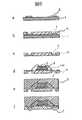
本願の第一の発明は、
1A.導電性仮支持体の片面に配線を形成する工程、
1B.配線が形成された導電性仮支持体に半導体素子を搭載し、半導体素子端子と配線を導通する工程、
1C.半導体素子を樹脂封止する工程、
1D.導電性仮支持体を除去し配線を露出する工程、
1E.露出された配線の外部接続端子が形成される箇所以外に絶縁層を形成する工程、
1F.配線の絶縁層が形成されていない箇所に外部接続端子を形成する工程
を含むことを特徴とする半導体パッケージの製造法である。(Disclosure of the Invention)
The first invention of the present application is
1A. Forming a wiring on one side of the conductive temporary support,
1B. A step of mounting a semiconductor element on a conductive temporary support on which wiring is formed, and conducting the semiconductor element terminal and the wiring;
1C. A step of resin-sealing a semiconductor element;
1D. Removing the conductive temporary support to expose the wiring;
1E. Forming an insulating layer other than where the external connection terminals of the exposed wiring are formed;
1F. A method of manufacturing a semiconductor package comprising a step of forming an external connection terminal at a location where an insulating layer of wiring is not formed.
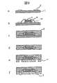
本願の第二の発明は、
2A.導電性仮支持体の片面に配線を形成する工程、
2B.配線が形成された導電性仮支持体の配線が形成された面に絶縁性支持体を形成する工程、
2C.導電性仮支持体を除去し配線を絶縁性支持体に転写する工程、
2D.配線の外部接続端子が形成される箇所の絶縁性支持体を除去し外部接続端子用透孔を設ける工程、
2E.配線が転写された絶縁性支持体に半導体素子を搭載し、半導体素子端子と配線を導通する工程、
2G.半導体素子を樹脂封止する工程、
2H.外部接続端子用透孔に配線と導通する外部接続端子を形成する工程
を含むことを特徴とする半導体パッケージの製造法である。The second invention of the present application is:
2A. Forming a wiring on one side of the conductive temporary support,
2B. Forming an insulating support on the surface of the conductive temporary support on which the wiring is formed;
2C. Removing the conductive temporary support and transferring the wiring to the insulating support;
2D. Removing the insulating support at the location where the external connection terminal of the wiring is formed and providing a through hole for the external connection terminal;
2E. A process of mounting a semiconductor element on an insulating support to which wiring is transferred, and conducting the semiconductor element terminal and the wiring;
2G. A step of resin-sealing a semiconductor element;
2H. A method of manufacturing a semiconductor package comprising a step of forming an external connection terminal that is electrically connected to a wiring in a through hole for an external connection terminal.
第二の発明に於いて、2A〜2Hの順に進めるのが好ましいが、2Dの工程を2Bの前に行うようにしても良い。例えば2Bの工程を外部接続端子用透孔を予め設けた絶縁フィルム絶縁性支持体を配線が形成された導電性仮支持体の配線が形成された面に貼り合わすことにより行っても良い。 In the second invention, it is preferable to proceed in the order of 2A to 2H, but the 2D process may be performed before 2B. For example, the process of 2B may be performed by bonding an insulating film insulating support provided with a through hole for an external connection terminal in advance to the surface of the conductive temporary support on which the wiring is formed.
本願の第三の発明は、
3A.導電性仮支持体の片面に配線を形成する工程、
3B.配線が形成された導電性仮支持体に半導体素子を搭載し、半導体素子端子と配線を導通する工程、
3C.半導体素子を樹脂封止する工程、
3D.配線の外部接続端子が形成される箇所以外の導電性仮支持体を除去し導電性仮支持体よりなる外部接続端子を形成する工程、
3E.外部接続端子の箇所以外に絶縁層を形成する工程、を含むことを特徴とする半導体パッケージの製造法である。The third invention of the present application is:
3A. Forming a wiring on one side of the conductive temporary support,
3B. A step of mounting a semiconductor element on a conductive temporary support on which wiring is formed, and conducting the semiconductor element terminal and the wiring;
3C. A step of resin-sealing a semiconductor element;
3D. Removing the conductive temporary support other than the portion where the external connection terminal of the wiring is formed to form an external connection terminal made of the conductive temporary support;
3E. And a step of forming an insulating layer in addition to the location of the external connection terminal.
本願の第四の発明は、
4A.導電性仮支持体の片面に配線を形成する工程、
4B.配線が形成された導電性仮支持体に半導体素子を搭載し、半導体素子端子と配線を導通する工程、
4C.半導体素子を樹脂封止する工程、
4D.導電性仮支持体の半導体素子搭載面と反対側の配線の外部接続端子が形成される箇所に、導電性仮支持体と除去条件が異なる金属パターンを形成する工程、
4E.金属パターンが形成された箇所以外の導電性仮支持体を除去する工程
を含むことを特徴とする半導体パッケージの製造法である。The fourth invention of the present application is:
4A. Forming a wiring on one side of the conductive temporary support,
4B. A step of mounting a semiconductor element on a conductive temporary support on which wiring is formed, and conducting the semiconductor element terminal and the wiring;
4C. A step of resin-sealing a semiconductor element;
4D. A step of forming a metal pattern having a different removal condition from the conductive temporary support at a position where the external connection terminal of the wiring on the side opposite to the semiconductor element mounting surface of the conductive temporary support is formed;
4E. A method of manufacturing a semiconductor package comprising a step of removing a conductive temporary support other than a portion where a metal pattern is formed.
金属パターンとしてははんだが好ましく、又ニッケル続いて金の層を積ねたものでも良い。 The metal pattern is preferably a solder, or may be a nickel layer followed by a gold layer.
本願の第五の発明は、
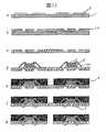
5A.絶縁性支持体の片面に複数組の配線を形成する工程、
5B.配線の外部接続端子となる箇所の絶縁性支持体を除去し外部接続端子用透孔を設ける工程
5C.複数組の配線が形成された絶縁性支持体に半導体素子を搭載し、半導体素子端子と配線を導通する工程、
5D.半導体素子を樹脂封止する工程、
5E.外部接続端子用透孔に配線と導通する外部接続端子を形成する工程、
5F.個々の半導体パッケ−ジに分離する工程
を含むことを特徴とする半導体パッケージの製造法である。The fifth invention of the present application is:
5A. Forming a plurality of sets of wirings on one side of the insulating support;
5B. Step 5C of removing an insulating support at a location to be an external connection terminal of wiring and providing a through hole for external connection terminal. A step of mounting a semiconductor element on an insulating support formed with a plurality of sets of wirings, and electrically connecting the semiconductor element terminals and the wiring;
5D. A step of resin-sealing a semiconductor element;
5E. Forming an external connection terminal that is electrically connected to the wiring in the through hole for the external connection terminal;
5F. A method of manufacturing a semiconductor package, comprising a step of separating into individual semiconductor packages.
第五の発明に於いて、製造工程は、5A〜5Fの順に進めるのが好ましいが、5A、5Bを逆にしても良い。すなわち外部接続端子用透孔を設けた絶縁性支持体に、複数組の配線を形成するようにしても良い。 In the fifth invention, it is preferable that the manufacturing process proceeds in the order of 5A to 5F, but 5A and 5B may be reversed. That is, a plurality of sets of wirings may be formed on the insulating support provided with the through holes for external connection terminals.
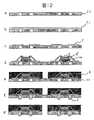
本願の第六の発明は、
6A.導電性仮支持体の片面に複数組の配線を形成する工程、
6B.導電性仮支持体に形成された複数組の配線を所定の単位個数になるように導電性仮支持体を切断分離し、配線が形成された分離導電性仮支持体をフレ−ムに固着する工程、
6C.配線が形成された導電性仮支持体に半導体素子を搭載し、半導体素子端子と配線を導通する工程、
6D.半導体素子を樹脂封止する工程、
6E.導電性仮支持体を除去し配線を露出する工程、
6F.露出された配線の外部接続端子が形成される箇所以外に絶縁層を形成する工程、
6G.配線の絶縁層が形成されていない箇所に外部接続端子を形成する工程
6H.個々の半導体パッケ−ジに分離する工程
を含むことを特徴とする半導体パッケージの製造法である。The sixth invention of the present application is:
6A. Forming a plurality of sets of wirings on one side of the conductive temporary support;
6B. The plurality of sets of wirings formed on the conductive temporary support are cut and separated so that a predetermined unit number is obtained, and the separated conductive temporary support on which the wiring is formed is fixed to the frame. Process,
6C. A step of mounting a semiconductor element on a conductive temporary support on which wiring is formed, and conducting the semiconductor element terminal and the wiring;
6D. A step of resin-sealing a semiconductor element;
6E. Removing the conductive temporary support to expose the wiring;
6F. Forming an insulating layer other than where the external connection terminals of the exposed wiring are formed;
6G. Step 6H of forming an external connection terminal at a location where the wiring insulation layer is not formed 6H. A method of manufacturing a semiconductor package, comprising a step of separating into individual semiconductor packages.
6Bの所定の単位個数は1個が好ましいが、生産性を上げるため複数個であっても良い。 The predetermined unit number of 6B is preferably one, but may be plural in order to increase productivity.
本願の第七の発明は、
7A.絶縁性支持体の片面に複数組の配線を形成する工程、
7B.配線の外部接続端子となる箇所の絶縁性支持体を除去し外部接続端子用透孔を設ける工程
7C.絶縁性支持体に形成された複数組の配線を所定の単位個数になるように絶縁性支持体を切断分離し、配線が形成された分離絶縁性支持体をフレ−ムに固着する工程、
7D.配線が形成された絶縁性支持体に半導体素子を搭載し、半導体素子端子と配線を導通する工程、
7E.半導体素子を樹脂封止する工程、
7F.外部接続端子用透孔に配線と導通する外部接続端子を形成する工程、
7G.個々の半導体パッケ−ジに分離する工程
を含むことを特徴とする半導体パッケージの製造法である。The seventh invention of the present application is
7A. Forming a plurality of sets of wirings on one side of the insulating support;
7B. Step 7C of removing an insulating support at a location to be an external connection terminal of wiring and providing a through hole for external connection terminal. Cutting and separating the insulating support so that a plurality of sets of wires formed on the insulating support have a predetermined unit number, and fixing the separated insulating support on which the wires are formed to the frame;
7D. Mounting a semiconductor element on an insulating support on which wiring is formed, and conducting the semiconductor element terminal and the wiring;
7E. A step of resin-sealing a semiconductor element;
7F. Forming an external connection terminal that is electrically connected to the wiring in the through hole for the external connection terminal;
7G. A method of manufacturing a semiconductor package, comprising a step of separating into individual semiconductor packages.
製造工程は、7A〜7Gの順に進めるのが好ましいが、第五の発明と同様7A、7Bを逆にしても良い。 The manufacturing process preferably proceeds in the order of 7A to 7G, but 7A and 7B may be reversed as in the fifth invention.
本願の第八の発明は、1層の配線においてその配線の片面が半導体素子と接続する第1の接続機能を持ち、その配線の反対側が外部の配線と接続する第2の接続機能をもつように構成された配線を備えた半導体パッケージの製造法であって、下記8A、8B、8C、8Dの工程を含むことを特徴とする半導体パッケージの製造法。
8A.耐熱性を有する金属箔付き絶縁基材の金属箔を複数組の配線パターンに加工する工程。
8B.後工程で第2の接続機能部となる位置に、絶縁基材側から配線パターンに達する凹部を設ける工程。
8C.配線パターン面及び配線パターンと隣接する絶縁基材面上の所望する位置に、所定の部分を開孔させたフレーム基材を貼り合わせる工程。
8D.半導体素子を搭載し半導体素子端子と配線を導通し半導体素子を樹脂封止する工程。The eighth invention of the present application has a first connection function in which one side of the wiring in one layer wiring connects to the semiconductor element, and a second connection function in which the opposite side of the wiring connects to an external wiring. A method for manufacturing a semiconductor package comprising wiring configured as described above, comprising the following steps 8A, 8B, 8C, and 8D.
8A. The process which processes the metal foil of the insulation base material with a metal foil which has heat resistance into several sets of wiring patterns.
8B. The process of providing the recessed part which reaches a wiring pattern from the insulating base material side in the position used as a 2nd connection function part in a post process.
8C. A step of bonding a frame substrate having a predetermined portion opened to a desired position on the wiring pattern surface and the insulating substrate surface adjacent to the wiring pattern.
8D. A step of mounting a semiconductor element, conducting the semiconductor element terminal and wiring, and sealing the semiconductor element with resin.
第八の発明に於いて、工程は8A〜8Dの順に進めるのが好ましいが、8Aと8Bを逆にしても良い。すなわち、絶縁基板に金属箔に達する凹を設けた後金属箔を配線パターンに加工するようにしても良い。 In the eighth invention, the steps are preferably carried out in the order of 8A to 8D, but 8A and 8B may be reversed. That is, the metal foil may be processed into a wiring pattern after providing a recess reaching the metal foil on the insulating substrate.
本願の第九の発明は、1層の配線においてその配線の片面が半導体素子と接続する第1の接続機能を持ち、その配線の反対側が外部の配線と接続する第2の接続機能をもつように構成された配線を備えた半導体パッケージの製造法であって、下記9A、9B、9C、9Dの工程を含むことを特徴とする半導体パッケージの製造法。
9A.耐熱性を有する金属箔付き絶縁基材の金属箔を複数組の配線パターンに加工する工程。
9B.後工程で第2の接続機能部となる位置に、絶縁基材側から配線パターンに達する凹部を設ける工程。
9C.配線パターン面及び配線パターンと隣接する絶縁基材面上の所望する位置に、所定の部分を開孔させた第2絶縁基材を貼り合わせ絶縁支持体を構成する工程。
9D.絶縁支持体に形成された複数組の配線を所定の単位個数になるように絶縁支持体を切断分離し、配線が形成された分離絶縁支持体をフレームに固着する工程。
9E.半導体素子を搭載し半導体素子端子と配線を導通し半導体素子樹脂封止する工程。According to a ninth aspect of the present application, in one layer of wiring, one side of the wiring has a first connection function of connecting to a semiconductor element, and the opposite side of the wiring has a second connection function of connecting to an external wiring. A method of manufacturing a semiconductor package comprising wiring configured as described above, comprising the following steps 9A, 9B, 9C, and 9D.
9A. The process which processes the metal foil of the insulation base material with a metal foil which has heat resistance into several sets of wiring patterns.
9B. The process of providing the recessed part which reaches a wiring pattern from the insulating base material side in the position used as a 2nd connection function part in a post process.
9C. A step of forming an insulating support by bonding a wiring pattern surface and a second insulating substrate having a predetermined portion opened at a desired position on an insulating substrate surface adjacent to the wiring pattern.
9D. A step of cutting and separating the insulating support so that a plurality of sets of wirings formed on the insulating support have a predetermined unit number, and fixing the separated insulating support formed with the wires to the frame.
9E. A step of mounting a semiconductor element, conducting the semiconductor element terminal and wiring, and encapsulating the semiconductor element with resin.
第九の発明に於いて、工程は9A〜9Eの順に進めるのが好ましいが、第八の発明と同様9Aと9Bを逆にしても良い。 In the ninth invention, the steps are preferably carried out in the order of 9A to 9E, but 9A and 9B may be reversed as in the eighth invention.
本願の第十の発明は、
10A.支持体の片面に複数組の配線を形成する工程、
10B.配線が形成された支持体に複数個の半導体素子を搭載し、半導体素子端子と配線とを導通させる工程、
10C.導通された複数組の半導体素子と配線とを一括して樹脂封止する工程、10D.支持体の所望する部分を除去して配線の所定部分を露出させ、露出した配線と電気的に接続した外部接続端子を形成する工程、
10E.個々の半導体パッケ−ジに分離する工程
を含むことを特徴とする半導体パッケージの製造法である。The tenth invention of the present application is:
10A. Forming a plurality of sets of wirings on one side of the support,
10B. Mounting a plurality of semiconductor elements on a support on which wiring is formed, and conducting the semiconductor element terminals and the wiring;
10C. A step of resin-sealing a plurality of conductive semiconductor elements and wirings collectively, 10D. Removing a desired portion of the support to expose a predetermined portion of the wiring, and forming an external connection terminal electrically connected to the exposed wiring;
10E. A method of manufacturing a semiconductor package, comprising a step of separating into individual semiconductor packages.
支持体として金属箔を使用し樹脂封止後に支持体を除去することにより配線パターンを露出させるようにしても良い。 A metal foil may be used as the support, and the wiring pattern may be exposed by removing the support after resin sealing.
又、支持体が絶縁基材で、樹脂封止後に絶縁基材の所定部分を除去して配線パターンに達する非貫通凹部を形成するようにすることもできる。 Alternatively, the support may be an insulating base material, and a predetermined portion of the insulating base material may be removed after resin sealing to form a non-penetrating recess that reaches the wiring pattern.
本願の第十一の発明は、複数個の半導体素子実装基板部を備え、複数個の半導体素子実装基板部を連結するための連結部を備え、位置合わせマーク部を備えている半導体素子実装用フレームの製造法であって、
(a)導電性仮基板上に半導体素子実装部の配線を作製する工程、
(b)樹脂基材上に配線を転写する工程、
(c)導電性仮基板をエッチング除去する工程、
を含み、(c)の導電性仮基板の除去に際して、導電性仮基板に一部を残し連結部の一部を構成するようにすることを特徴とする半導体素子実装用フレームの製造法である。An eleventh invention of the present application includes a plurality of semiconductor element mounting substrate portions, a connecting portion for connecting the plurality of semiconductor element mounting substrate portions, and an alignment mark portion. A method of manufacturing a frame,
(A) producing a wiring for a semiconductor element mounting portion on a conductive temporary substrate;
(B) a step of transferring the wiring onto the resin substrate;
(C) a step of removing the conductive temporary substrate by etching;
And (c) a method of manufacturing a frame for mounting a semiconductor element, wherein a part of the connecting portion is formed by leaving a part of the conductive temporary substrate when the conductive temporary substrate is removed. .
本発明では、半導体素子はLSIチップ、ICチップ等通常の素子が使用できる。 In the present invention, a normal element such as an LSI chip or an IC chip can be used as the semiconductor element.
半導体素子端子と配線とを同通する方法には、ワイヤボンディングだけでなく、バンプ、異方導電性フィルム等通常の手段を用いることができる。 As a method for allowing the semiconductor element terminal and the wiring to communicate with each other, not only wire bonding but also normal means such as a bump and an anisotropic conductive film can be used.
本発明においては、半導体素子を樹脂封止した後、封止樹脂硬化物を加熱処理することにより、そり、変形のない半導体パッケージを製造することができる。 In the present invention, a semiconductor package free from warpage and deformation can be produced by heat-treating the cured resin product after resin-sealing the semiconductor element.
加熱処理は、封止樹脂硬化物のガラス転移温度±20℃の温度が好ましい。この理由は、ガラス転移温度±20℃の範囲で樹脂硬化物は最も塑性的な性質が強く、残留歪みを解消し易いためである。加熱処理の温度が、ガラス転移温度−20℃未満では樹脂硬化物はガラス状態の弾性体となり緩和の効果が少なくなる傾向があり、ガラス転移温度+20℃を超えれば樹脂硬化物はゴム弾性体となり同様に歪みを解消する効果がすきなくなる傾向にある。 The heat treatment is preferably performed at a glass transition temperature ± 20 ° C. of the cured encapsulated resin. This is because the cured resin has the strongest plastic property within the range of the glass transition temperature ± 20 ° C., and it is easy to eliminate the residual strain. When the temperature of the heat treatment is less than the glass transition temperature of −20 ° C., the cured resin tends to be an elastic body in a glass state, and the effect of relaxation tends to be reduced. Similarly, the effect of eliminating distortion tends to be lost.
封止樹脂硬化物のガラス転移温度±20℃の温度で加熱処理をした後、5℃/分以下の降温速度で室温まで冷却することにより、半導体パッケ−ジのそり、変形をより確実に防止することができる。 Heat treatment at a glass transition temperature of ± 20 ° C of the cured encapsulated resin and then cooling to room temperature at a rate of 5 ° C / min or less can prevent the semiconductor package from warping and deformation more reliably. can do.
加熱処理及び/又は冷却の工程は、封止樹脂硬化物の上下面を剛性平板で、封止樹脂硬化物のそり、変形を押さえる力で押圧した状態で行うのが好ましい。 The heat treatment and / or cooling step is preferably carried out in a state where the upper and lower surfaces of the cured encapsulated resin are pressed by a rigid flat plate with a force that suppresses warpage and deformation of the encapsulated cured resin.
本発明の半導体パッケージにおいては、配線は1層の配線においてその配線の片面が半導体チップと接続する第1の接続機能を持ち、その配線の反対面が外部の配線と接続する第2の接続機能をもつように構成されている。 In the semiconductor package of the present invention, the wiring has a first connection function in which one side of the wiring is connected to the semiconductor chip in a single layer wiring, and the second connection function is connected to the external wiring on the opposite side of the wiring. It is comprised so that it may have.
外部の配線と接続する外部接続端子は、例えばはんだバンプ、金バンプ等が好的に使用できる。 For example, solder bumps and gold bumps can be preferably used as the external connection terminals connected to the external wiring.
外部接続端子は、半導体素子端子が配線とワイヤボンディング等で導通される位置より内側に設けるようにするのが高密度化の上で好ましい(ファンインタイプ)。このように外部接続端子の位置は、半導体素子が搭載された下面に格子状に配置するのが高密度化の上で好ましい。 It is preferable to provide the external connection terminals on the inner side from the position where the semiconductor element terminals are electrically connected to the wiring by wire bonding or the like (fan-in type). As described above, the external connection terminals are preferably arranged in a grid pattern on the lower surface on which the semiconductor element is mounted in terms of increasing the density.
(発明を実施するための最良の形態)
図1により、本発明の第一の実施例について説明する。(Best Mode for Carrying Out the Invention)
The first embodiment of the present invention will be described with reference to FIG.
厚さ0.035mmの電解銅箔1の片面に厚さ0.001mmのニッケル層(図1では省略)をめっきする。次に、感光性ドライフィルムレジスト(日立化成工業(株)製、商品名:フォテックHN340)をラミネートし、配線パターンを露光、現像し、めっきレジストを形成する。続いて、硫酸銅浴にて電解銅めっきを行う。さらに、ニッケルめっきを0.003mm、純度99.9%以上の金めっきを0.0003mm以上の厚さでめっきする。次に、めっきレジストを剥離し、配線2を形成する(図1a)。このようにして、配線2を形成した銅箔1にLSIチップ3を搭載する(図1b)。LSIチップの接着には、半導体用銀ペースト4を用いた。次にLSI端子部と配線2とをワイヤボンド100により接続する(図1c)。このようにして形成したものをトランスファモールド金型に装填し、半導体封止用エポキシ樹脂(日立化成工業(株)製、商品名:CL−7700)を用いて封止5した(図1d)。その後、銅箔1のみをアルカリエッチャントで溶解除去し、ニッケルを露出させた。ニッケル層を銅の溶解性の少ないニッケル剥離液にて除去して、配線部を露出させた(図1e)。続いて、ソルダレジスト6を塗布し、接続用端子部を露出するようにパターンを形成した。この配線露出部に、はんだボール7を配置し溶融させた(図1f)。このはんだボール7を介して外部の配線と接続する。 A nickel layer (not shown in FIG. 1) having a thickness of 0.001 mm is plated on one surface of an
図2により、本発明の第二の実施例について説明する。 The second embodiment of the present invention will be described with reference to FIG.
図1の場合と同様の方法で、配線2を有する銅箔1を作成した(図2a)。LSIチップ3を搭載する。LSIチップには、端子部に金バンプ8を形成し、この金バンプ8と配線2の端子部とを加熱加圧して接続する(図2b)。次に、LSIチップ下部に液状エポキシ樹脂を充填し硬化9させる(図2c)。このようにして形成したものをトランスファモールド金型に装填し、半導体封止用エポキシ樹脂(日立化成工業(株)製、商品名:CL−7700)を用いて封止10した(図2d)。その後、銅箔1のみをアルカリエッチャントで溶解除去し、ニッケルを露出させた。ニッケル層を銅の溶解性の少ないニッケル剥離液にて除去して、配線部を露出させた(図2e)。続いて、ソルダレジスト6を塗布し、接続用端子部を露出するようにパターンを形成した。この配線露出部に、はんだボール7を配置し溶融させた(図2f)。このはんだボール7を介して外部の配線と接続する。 A
図3により、本発明の第三の実施例について説明する。 A third embodiment of the present invention will be described with reference to FIG.
厚さ0.035mmの電解銅箔1の片面に厚さ0.001mmのニッケル層(図3では省略)をめっきする。次に、感光性ドライフィルムレジスト(日立化成工業(株)製、商品名:フォテックHN340)をラミネートし、配線パターンを露光、現像しめっきレジストを形成する。続いて、硫酸銅浴にて電解銅めっきを行い、第一の配線13を形成する。次にめっきレジストを剥離し、第一の配線13の表面を酸化処理、還元処理を行う。新たな銅箔と接着樹脂としてポリイミド系接着フィルム(日立化成工業(株)製、商品名:AS2210)12を用いて配線13が内側となるように積層接着する。(銅箔11に直径0.1mmの穴を通常のフォトエッチング法により形成する。パネルめっき法により、穴内と銅箔表面全体を銅めっきする。)銅箔をフォトエッチング法で第二の配線11を形成する。LSI搭載部の樹脂(ポリイミド系接着フィルム12)をエキシマレーザにより除去し端子部を露出させる。該端子部に、ニッケルめっきを0.003mm、純度99.9%以上の金めっきを0.0003mm以上の厚さでめっきする(図3a)。このようにして、2層配線を形成した銅箔1にLSIチップを搭載する。LSIチップの接着には、半導体用銀ペーストを用いた(図3b)。次にLSI端子部と配線13とをワイヤボンド100により接続する(図3c)。このようにして形成したものをトランスファモールド金型に装填し、半導体封止用エポキシ樹脂(日立化成工業(株)製、商品名:CL−7700)を用いて封止5した。その後、銅箔1のみをアルカリエッチャントで溶解除去し、ニッケルを露出させた。ニッケル層を銅の溶解性の少ないニッケル剥離液にて除去して、配線部を露出させた(図3e)。続いて、ソルダレジスト6を塗布し、接続用端子部を露出するようにパターンを形成した。該露出部に、はんだボール7を配置し溶融させた(図3f)。このはんだボール7を介して外部の配線と接続する。 A nickel layer (not shown in FIG. 3) having a thickness of 0.001 mm is plated on one surface of the
図4により、本発明の第四の実施例について説明する。 A fourth embodiment of the present invention will be described with reference to FIG.
厚さ0.1mmのSUS(ステンレス鋼)板14に、感光性ドライフィルムレジスト(日立化成工業(株)製、商品名:フォテックHN340)をラミネートし、配線パターンを露光、現像し、めっきレジストを形成する。続いて、硫酸銅浴にて電解銅めっきを行う。さらに、ニッケルめっきを0.003mm、純度99.9%以上の金めっきを0.0003mm以上の厚さでめっきする。次に、めっきレジストを剥離し、配線2を形成する(図4a)。このようにして配線2を形成したSUS板14に半導体チップ103を搭載する(図4b)。半導体チップの接着には半導体用銀ベースト4を用いた。次に半導体端子部と配線2とをワイヤボンド100により接続する(図4c)。このようにして形成したものをトランスファモールド金型に装填し、半導体封止用エポキシ樹脂(日立化成工業(株)製、商品名:CL−7700)を用いて封止5した(図4d)。その後、SUS板14を機械的に剥離除去し、配線部を露出させた(図4e)。続いてソルダレジスト6を塗布し、接続用端子部を露出するようにパターンを形成した。この配線露出部にはんだボール7を配置し溶融させた(図4f)。このはんだボール7を介して外部の配線と接続する。 A photosensitive dry film resist (manufactured by Hitachi Chemical Co., Ltd., trade name: Photec HN340) is laminated on a SUS (stainless steel) plate 14 having a thickness of 0.1 mm, and the wiring pattern is exposed and developed, and the plating resist is applied. Form. Subsequently, electrolytic copper plating is performed in a copper sulfate bath. Further, nickel plating is plated with a thickness of 0.003 mm and gold plating with a purity of 99.9% or more is 0.0003 mm or more. Next, the plating resist is removed to form the wiring 2 (FIG. 4a). The
図5により、本発明の第五の実施例について説明する。 The fifth embodiment of the present invention will be described with reference to FIG.
厚さ0.035mmの電解銅箔1に、感光性ドライフィルムレジスト(日立化成工業(株)製、商品名:フォテックHN340)をラミネートし、配線パターンを露光、現像し、めっきレジストを形成する。続いてニッケルのパターンめっき15を行った後、硫酸銅浴にて電解銅めっきを行う。さらに、ニッケルめっきを0.003mm、純度99.9%以上の金めっきを0.0003mm以上の厚さでめっきする。次に、めっきレジストを剥離し、配線2を形成する(図5a)。このようにして配線2を形成した銅箔1に半導体チップ103を搭載する(図5b)。半導体チップの接着には、半導体用銀ベースト4を用いた。次に半導体端子部と配線2とをワイヤボンド100により接続する(図5c)。このようにして形成したものをトランスファモールド金型に装填し、半導体封止用エポキシ樹脂(日立化成工業(株)製、商品名:CL−7700)を用いて封止5した(図5d)。その後、銅箔1をアルカリエッチャンで溶解除去し、ニッケルの配線部を露出させた(図5e)。続いてソルダレジスト6を塗布し、接続用端子部を露出するようにパターンを形成した。この配線露出部にはんだボール7を配置し溶融させた(図5f)。このはんだボール7を介して外部の配線と接続する。 A photosensitive dry film resist (manufactured by Hitachi Chemical Co., Ltd., trade name: Photec HN340) is laminated on the
図6により、本発明の第六の実施例について説明する。 The sixth embodiment of the present invention will be described with reference to FIG.
厚さ0.035mmの電解銅箔1に、感光性ドライフィルムレジスト(日立化成工業(株)製、商品名:フォテックHN340)をラミネートし、配線パターンを露光、現像し、めっきレジストを形成する。続いて純度99.9%以上の金めっきを0.0003mm、ニッケルめっきを0.003mm以上の厚さでめっきする。さらに、硫酸銅浴にて電解銅めっきを行い、めっきレジストを剥離し、配線2を形成する(図6a)。このようにして配線2を形成した銅箔1の配線面にポリイミドフィルム16を接着し、レーザを用いて配線2の接続用端子部を露出させ(図6b)、銅箔1をエッチングで除去する(図6c)。また、ポリイミドの代わりに、感光性フィルムを用いることで、レーザを使用しないで接続用端子部を露出させることができる。続いて、ポリイミドフィルム16の配線パターン面にLSIチップ3を搭載する。LSIチップの接着には半導体用銀ペースト4を用いた。次に半導体端子部と配線2とをワイヤボンド100により接続する(図6d)。このようにして形成したものをトランスファモールド金型に装填し、半導体封止用エポキシ樹脂(日立化成工業(株)製、商品名:CL−7700)を用いて封止5する(図6e)。その後、接続用端子部にはんだボール7を配置し溶融させる(図6f)。このはんだボール7を介して外部の配線と接続する。 A photosensitive dry film resist (manufactured by Hitachi Chemical Co., Ltd., trade name: Photec HN340) is laminated on the
図7により、本発明の第七の実施例について説明する。 The seventh embodiment of the present invention will be described with reference to FIG.
厚さ0.035mmの電解銅箔1の片面に厚さ0.001mmのニッケル層(図7では省略)をめっきする。次に、感光性ドライフィルムレジスト(日立化成工業(株)製、商品名:フォテックHN340)をラミネートし、配線パターンを露光、現像し、めっきレジストを形成する。続いて硫酸銅浴にて電解銅めっきを行う。さらに、ニッケルめっきを0.003mm、純度99.9%以上の金めっきを0.0003mm以上の厚さでめっきする。次にめっきレジストを剥離し、配線2を形成する(図7a)。このようにして配線2を形成した銅箔1にLSIチップ3を搭載する。LSIチップの接着には半導体用銀ペースト4を用いた。次に、半導体端子部と配線2とをワイヤボンド100により接続する(図7b)。このようにして形成したものをトランスファモールド金型に装填し半導体封止用エポキシ樹脂(日立化成工業(株)製、商品名:CL−7700)を用いて封止5する(図7c)。その後、銅箔1のみをアルカリエッチャントで溶解除去し、ニッケルを露出させる。ニッケル層を銅の溶解性の少ないニッケル剥離液にて除去して配線部を露出させる(図7d)。続いて、接続用端子部を開口させたポリイミドフィルム16を接着し(図7e)、この配線露出部にはんだボール7を配置し溶融させる(図7f)。このはんだボール7を介して外部の配線と接続する。 A nickel layer (not shown in FIG. 7) having a thickness of 0.001 mm is plated on one surface of the
図8により、本発明の第八の実施例について説明する。 An eighth embodiment of the present invention will be described with reference to FIG.
厚さ0.035mmの電解銅箔1に、感光性ドライフィルムレジスト(日立化成工業(株)製、商品名:フォテックHN340)をラミネートし、配線パターンを露光、現像し、めっきレジストを形成する。続いて純度99.9%以上の金めっきを0.0003mm、ニッケルめっきを0.003mm以上の厚さでめっきする。さらに、硫酸銅浴にて電解銅めっきを行い、めっきレジストを剥離し配線2を形成する(図8a)。このようにして配線2を形成した銅箔1の配線面に液状封止樹脂17をスクリーン印刷により塗布し、配線2の接続用端子部を露出させるようにして絶縁層を形成する(図8b)。液状封止樹脂を硬化させた後、銅箔1をエッチングで除去する(図8c)。続いて、硬化させた液状封止樹脂3の配線パターン面にLSIチップ3を搭載する。LSIチップの接着には半導体用銀ペースト4を用いた。次に半導体端子部と配線2とをワイヤボンド100により接続する(図8d)。このようにして形成したものをトランスファモールド金型に装填し、半導体封止用エポキシ樹脂(日立化成工業(株)製、商品名:CL−7700)を用いて封止5する(図8e)。その後、配線2の接続用端子部にはんだボール7を配置し溶融させる(図8f)。このはんだボール7を介して外部の配線と接続する。 A photosensitive dry film resist (manufactured by Hitachi Chemical Co., Ltd., trade name: Photec HN340) is laminated on the
図9により、本発明の第九の実施例について説明する。 A ninth embodiment of the present invention will be described with reference to FIG.
厚さ0.035mmの電解銅箔1の片面に厚さ0.001mmのニッケル層(図9では省略)をめっきする。次に、感光性ドライフィルムレジスト(日立化成工業(株)製、商品名:フォテックHN340)をラミネートし、配線パターンを露光、現像し、めっきレジストを形成する。続いて硫酸銅浴にて電解銅めっきを行う。さらに、ニッケルめっきを0.003mm、純度99.9%以上の金めっきを0.0003mm以上の厚さでめっきする。次にめっきレジストを剥離し、配線2を形成する(図9a)。このようにして配線2を形成した銅箔1にLSIチップ3を搭載する。LSIチップ3の接着には半導体用銀ペースト4を用いた。次に、半導体端子部と配線2とをワイヤボンド100により接続する(図9b)。このようにして形成したものをトランスファモールド金型に装填し半導体封止用エポキシ樹脂(日立化成工業(株)製、商品名:CL−7700)を用いて封止5する(図9c)。その後、銅箔1のみをアルカリエッチャントで溶解除去し、ニッケルを露出させる。ニッケル層を銅の溶解性の少ないニッケル剥離液にて除去して配線部を露出させる(図9d)。続いて、液状封止樹脂17をスクリーン印刷により塗布し、配線2の接続用端子部を露出させるようにして、液状封止樹脂17の絶縁層を形成する(図9e)。この配線2の接続用端子部にはんだボール7を配置し溶融させる(図9f)。このはんだボール7を介して外部の配線と接続する。 A nickel layer (not shown in FIG. 9) having a thickness of 0.001 mm is plated on one surface of the
図10により、本発明の第十の実施例について説明する。 A tenth embodiment of the present invention will be described with reference to FIG.
厚さ0.035mmの電解銅箔1の片面に厚さ0.001mmのニッケル層(図10では省略)をめっきする。次に、感光性ドライフィルムレジスト(日立化成工業(株)製、商品名:フォテックHN340)をラミネートし、配線パターン及び位置合わせマークのめっきレジストを露光、現像により形成する。続いて、硫酸銅浴にて電解銅めっきを行う。さらに、ニッケルめっきを0.003mm、純度99.9%以上の金めっきを0.0003mm以上の厚さでめっきする。次に、めっきレジストを剥離し、配線2及び位置合わせマーク18を形成した後(図10a)、位置合わせマーク18の部分だけをSUS板で挟みプレスすることで銅箔1の裏面に位置合わせマークを浮かび上がらせる(図10b)。このようにして配線2及び位置合わせマーク18を形成した銅箔1にLSIチップ3を搭載する(図10c)。LSIチップ3の接着には半導体用銀ペースト4を用いた。次に、半導体端子部と配線2とをワイヤボンド100により接続する(図10d)。このようにして形成したものをトランスファモールド金型に装填し、半導体封止用エポキシ樹脂(日立化成工業(株)製、商品名:CL−7700)を用いて封止5した(図10e)。銅箔裏側に再び感光性ドライフィルムをラミネートし、位置合わせマーク18を利用してエッチングパターン形成する。その後、銅箔1及びニッケル層をエッチングして、銅箔1によるバンプ7の形成及び配線部の露出を行う(図10f)。続いて、ソルダレジスト8を塗布し、バンプ7が露出するように絶縁層を形成した(図10g)。このバンプ7を介して外部の配線と接続する。 A nickel layer (not shown in FIG. 10) having a thickness of 0.001 mm is plated on one surface of the
図11により、本発明の第十一の実施例について説明する。 An eleventh embodiment of the present invention will be described with reference to FIG.
厚さ0.035mmの電解銅箔1に、感光性ドライフィルムレジスト(日立化成工業(株)製、商品名:フォテックHN340)をラミネートし、複数組の配線パターンを露光、現像し、めっきレジストを形成する。続いて、純度99.9%以上の金めっきを0.0003mm、ニッケルめっきを0.003mm以上の厚さでめっきする。さらに、硫酸銅浴にて電解銅めっきを行い、レジストを剥離し、複数組の配線2を形成する(図11a)。このようにして、複数組の配線2を形成した銅箔1の配線面にポリイミドフィルム19を接着し、レーザを用いて配線2の接続端子部を露出させ(図11b)、銅箔1をエッチングで除去する(図11c)。以上のように、1枚のポリイミドフィルム上に複数組の配線2を形成した後、LSIチップ3を搭載する。LSIチップの接着には、半導体用ダイボンディングテープ4’を用いた。次に半導体端子部と配線2とをワイヤボンド100により接続する(図11d)。このようにして形成したものをトランスファモールド金型に装填し、半導体封止用エポキシ樹脂(日立化成工業(株)製、商品名:CL−7700)を用いて各々封止5する(図11e)。その後、配線2の接続端子部にはんだボール7を配置し溶融させる(図11f)。このはんだボール7を介して外部の配線と接続する。最後にポリイミドフィルムで連結されたパッケージを、金型で打ち抜く(図11g)。 A photosensitive dry film resist (manufactured by Hitachi Chemical Co., Ltd., trade name: Photec HN340) is laminated on the
図12により、本発明の第十二の実施例について説明する。 A twelfth embodiment of the present invention will be described with reference to FIG.
厚さ0.07mmの接着剤付きポリイミドフィルム20を、金型で打ち抜き接続端子部となる部分を開口させる(図12a)。次に、厚さ0.035mmの銅箔21を接着後(図12b)、感光性ドライフィルムレジスト(日立化成工業(株)製、商品名:フォテックHN340)をラミネートし、複数組の配線パターンを露光、現像し、エッチングレジストを形成する。続いて銅箔をエッチングし、レジストを剥離し、複数組の配線2を形成する(図12c)。以上のように、1枚のポリイミドフィルム上に複数組の配線パターンを形成した後、LSIチップ3を搭載する。LSIチップ3の接着には、半導体用ダイボンディングテープ4’を用いた。次に半導体端子部と配線2とをワイヤボンド100により接続する(図12d)。このようにして形成したものをトランスファモールド金型に装填し、半導体封止用エポキシ樹脂(日立化成工業(株)製、商品名:CL−7700)を用いて各々封止5する(図12e)。その後、配線の接続端子部にはんだボール7を配置し溶融させる(図12f)。このはんだボール7を介して外部の配線と接続する。最後にポリイミドフィルムで連結されたパッケージを、金型で打ち抜く(図12g)。 A
図13〜15により、本発明の第十三の実施例について説明する。 A thirteenth embodiment of the present invention will be described with reference to FIGS.
厚さ0.035mmの電解銅箔1の片面に厚さ0.001mmのニッケル層(図13では省略)をめっきする。感光性ドライフィルムレジスト(日立化成工業(株)製、商品名:フォテックHN340)をラミネートし、複数組の配線パターンのめっきレジストを露光、現像により形成する。続いて、硫酸銅浴にて電解銅めっきを行う。さらに、ニッケルめっきを0.003mm、純度99.9%以上の金めっきを0.0003mm以上の厚さでめっきし、めっきレジストを剥離し、配線2を形成した(図13a)。次に、配線2を形成した銅箔1を単位個数に分けた後、ポリイミド接着フィルムを介して別に用意したステンレス製フレーム22(厚さ;0.135mm)にはりつけた(図13b)。フレームとしては、りん青銅等の銅合金、銅箔、ニッケル箔、ニッケル合金箔等が使用できる。接着の方法としては他に金属間の共晶を利用した接合、超音波を利用した接合等を用いることも可能である。また、図14に示したように銅箔1上の配線をあらかじめ検査し、配線良品23だけを撰択し、フレーム22にはりつけると良い。図14において、1は電解銅箔、22はフレ−ム、24は配線不良品、25は位置合わせ用穴である。また、この実施例では、切り分けた銅箔上には配線1個となるようにしたが、切り分けた銅箔上に複数組の配線があるようにしても良い。フレーム22と配線付き銅箔との張り合わせの位置関係として、例えば図15(a)、(b)に示したものなど種々可能である。図15はフレ−ム22の平面図であり、26はフレ−ム開口部、27は配線付き銅箔の搭載位置、28は箔固定用接着剤である。次に、LSIチップ3を搭載し、半導体端子部と配線2とをワイヤボンド100により接続する(図13c)。LSIチップの搭載には半導体用ダイボンディングテープ4’を用いた。ここで、ボンディングテープ4’の代わりにダイボンド用銀ペースト等を用いてもよい。また、半導体チップの実装には、通常のワイヤーボンディング接続を用いたが、フィリップチップ等、他の方法を用いてもよい。このようにして形成したものをトランスファモールド金型に装填し、半導体封止用エポキシ樹脂(日立化成工業(株)製、商品名:CL−7700)を用いて封止5した(図13d)。その後、銅箔1のみをアルカリエッチャントで溶解除去し、ニッケルを露出させた。ニッケル層を銅の溶解性の少ないニッケル剥離液にて除去して、配線部を露出させた。続いて、ソルダレジスト6を塗布し、接続用端子部を露出するようにパターンを形成した。この配線露出部に、はんだボール7を配置し溶融させた(図13e)。この後で、切断機を用いて切断し、フレーム22の不要な切片101を除いて、個々の半導体パッケージに分割した(図13f)。このはんだボール7を介して外部の配線と接続する。この例では、板取りを上げて効率よく半導体パッケ−ジを製造することができる。 A nickel layer (not shown in FIG. 13) having a thickness of 0.001 mm is plated on one surface of the
図16により、本発明の第十四の実施例について説明する。 A fourteenth embodiment of the present invention will be described with reference to FIG.
厚さ0.07mmの接着剤付きポリイミドフィルム29を、金型で打ち抜き接続端子部となる部分を開口させる。次に、厚さ0.035mmの銅箔を接着後、感光性ドライフィルムレジスト(日立化成工業(株)製、商品名:フォテックHN340)をラミネートし、複数組の配線パターンを露光、現像し、エッチングレジストを形成た。続いて銅箔をエッチングし、レジストを剥離し、複数組の配線2を形成する(図16a)。ここで、銅箔上にポリイミドを直接コ−ティングした材料(例えば、日立化成工業(株)製、商品名50001)を用いて、接続端子部および配線2を形成するようにしても良い。開口部の形成もドリル加工、エキシマレ−ザ等のレ−ザ加工、印刷等の方法を用いたり、ポリイミドに感光性を持たせた材料を使用し、露光・現像により形成しても良い。ポリイミドの代わりに封止樹脂等他の材料を使用しても良い。 A
以上のように、1枚のポリイミドフィルム上に複数組の配線パターンを形成した後、配線付きフィルムを単位個数に分けた、ポリイミド接着接着剤28を介して別に用意したステンレス製フレーム22(厚さ;0.135mm)にはりつけた(図16b)。次に、LSIチップ3を搭載し、半導体端子部と配線2とをワイヤボンド100により接続する(図16c)。LSIチップの搭載には半導体用ダイボンディングテープ4´を用いた。このようにして形成したものをトランスファモールド金型に装填し、半導体封止用エポキシ樹脂(日立化成工業(株)製、商品名:CL−7700)を用いて封止5した(図16d)。続いて最初に設けた接続端子部となるべき開口部にはんだボール7を配置し溶融させる(図16e)。このはんだボール7を介して外部の配線と接続する。最後にフレームで連結されたパッケージを金型で打ち抜き、個々のパッケージに分割した(図16f)。 As described above, after forming a plurality of sets of wiring patterns on a single polyimide film, the stainless steel frame 22 (thickness) prepared separately via the
図17により本発明の第十五の実施例について説明する。 A fifteenth embodiment of the present invention will be described with reference to FIG.
金属箔31上に絶縁基材32を直接形成した2層フレキシブル基材(図17a)の金属箔上に所定のレジスト像を形成し、公知のエッチング法により所望する複数組の配線パターン33を形成し、レジスト像を剥離する(図17b)。金属箔としては、電解銅箔や圧延銅箔あるいは銅合金箔などの単一箔の他、後工程で除去可能なキャリヤ箔上に銅薄層を有する複合金属箔なども適用可能である。具体的には、厚さ18μmの電解銅箔の片面に厚さ0.2μm程度のニッケル−リンめっき層を形成後、続けて厚さ5μm程度の銅薄層をめっきしたものなどが適用できる。この場合、銅薄層上にポリイミド層を形成した後、銅箔及びニッケル−リン層をエッチング除去することにより、銅薄層が露出する。すなわち、本願の発明においては銅薄層全てを露出させた後銅薄層を配線加工しても良いし、キャリヤ箔(銅箔/ニッケル薄層)をリードフレーム構造体の一部として利用しても良い。一方、絶縁基材としては、プロセス耐熱性などの観点からポリイミド材が一般的である。この場合、ポリイミドと銅箔の熱膨張係数が異なるとはんだリフロー工程において基材の反りが顕著になるため、ポリイミドとしては(化1)の繰り返し単位を有するポリイミドを70モル%以上含んだポリイミドを適用することが好ましい。 A predetermined resist image is formed on the metal foil of a two-layer flexible base material (FIG. 17a) in which the insulating

次に、後工程で外部基板との接続部となる位置に銅箔に達する凹部34を設ける(図17c)。凹部の加工方法は特に限定するものではなく、エキシマレーザや炭酸ガスレーザ及びYAGレーザなどレーザ加工の他、ウエットエッチング法などが適用可能である。 Next, a
次に、所定の部分(開孔部35)をパンチング加工等で打ち抜いた接着材36付きフレーム基材37を配線パターン面に接着させる(図17d)。この場合、フレーム基材は特に限定するものではなく、ポリイミドフィルムや銅箔などの金属箔の適用が可能である。ここで、仮に2層フレキシブル基材のポリイミド層厚さが25μmで、かつ、接着するフレーム基材がポリイミドフィルムの場合、フレーム全体としての剛直性を確保するためにはフィルム厚さとして50〜70μm程度が必要になる。なお、フレーム基材層を形成する領域についても特に限定するものではなく、半導体チップを搭載する部分にフレーム基材層を設けることも可能である。具体的には、チップ実装がワイヤボンディング方式の場合には、最小限ワイヤボンド用端子部38が露出していれば他の領域全てにフレーム基材層を設けても良い。次に、半導体チップ39を搭載し、金ワイヤ40で半導体チップと配線パターン間を電気的に接続させる(図17e)。一方、半導体チップ実装方式としてフェースダウン方式を採用する場合には、配線パターンの所定位置(半導体チップの外部接続用電極位置に対応)に金属パンプ等を設け、金属バンプを介して半導体チップと波線パターンとを電気的に接続させても良い。次に、トランスファーモールド用の金型にセットし、樹脂封止材41で封止する(図17f)。この場合、樹脂封止材は特に限定するものではなく、例えば、直径10〜20μm程度のシリカを5〜80wt%の範囲で含有したエポキシ系樹脂などが適用できる。次に、外部基板との接続部42を形成する。接続部42の形成方法としては、図17cの工程後にあらかじめ電解めっき法によりポリイミドフィルム厚さ以上のバンプを形成しておく方法や樹脂封止後にはんだ印刷法によりはんだバンプを形成する方法などが適用可能である。最後に、フレームからパッケージ部を切断して所望するパッケージが得られる(図17g)。 Next, a
図17の第十五の実施例を更に具体的に説明する。 The fifteenth embodiment of FIG. 17 will be described more specifically.
具体例1
厚さ12μmの電解銅箔を片面に有する2層フレキシブル基材(日立化成工業(株)製、商品名:MCF 5000I)の銅箔面上にドライフィルムレジスト(日立化成工業(株)製、商品名:フォテックHK815)をラミネートし、露光、現像により所望するレジストパターンを得た。次に、塩化第二鉄溶液で銅箔をエッチング加工後、レジストパターンを水酸化カリウム溶液で剥離することにより所定の配線パターンを得た。次に、エキシマレーザ加工機(住友重機械工業(株)製、装置名:INDEX200)を用いて絶縁基材側から配線パターン裏面に達する凹部(直径300μm)を所定の位置に所定の数だけ形成した。エキシマレーザ加工条件は、エネルギー密度250mJ/cm2、縮小率3.0、発振周波数200Hz、照射パルス数300パルスである。次に50μm厚さのポリイミドフィルム(宇部興産製、商品名:UPILEX S)の片面に厚さ10μmのポリイミド系接着材(日立化成工業(株)製、商品名:AS 2250)を有する接着シートを作製し、後工程でのワイヤボンド端子部に相当する領域を含む所定領域をパンチ加工により除去し、接着材を介してポリイミドフィルムと配線パターン付き2層フレキ基材とを加熱圧着させた。圧着条件は、圧力20kgf/cm2、温度180℃、加熱加圧時間60分である。次に、無電解ニッケル、金めっき法によりワイヤボンド用端子部にニッケル/金めっきを施した。めっき厚さは、それぞれ、3μm、0.3μmである。次に、半導体チップ搭載用ダイボンド材(日立化成工業(株)製、商品名:HM−1)を用いて半導体チップを搭載した。搭載条件は、プレス圧力5kgf/cm2、接着温度380℃及び圧着時間5秒である。次に、ワイヤボンディングにより半導体チップの外部電極部と配線パターンを電気的に接続した。その後、リードフレーム状に金型加工し、トランスファーモールド用金型にセットし、半導体封止用エポキシ樹脂(日立化成工業(株)製、CL−7700)を用いて185℃、90秒で封止した。続いて、前述の凹部に所定量のはんだを印刷塗布し、赤外線リフロー炉によりはんだを溶融させて外部接続用バンプを形成した。最後に、パッケージ部を金型で打ち抜き、所望するパッケージを得た。Example 1
A dry film resist (manufactured by Hitachi Chemical Co., Ltd.) on a copper foil surface of a two-layer flexible substrate (manufactured by Hitachi Chemical Co., Ltd., trade name: MCF 5000I) having an electrolytic copper foil having a thickness of 12 μm on one side. Name: Photec HK815) was laminated, and a desired resist pattern was obtained by exposure and development. Next, after etching the copper foil with a ferric chloride solution, a predetermined wiring pattern was obtained by peeling the resist pattern with a potassium hydroxide solution. Next, by using an excimer laser processing machine (manufactured by Sumitomo Heavy Industries, Ltd., device name: INDEX200), a predetermined number of recesses (diameter 300 μm) reaching the back surface of the wiring pattern from the insulating substrate side are formed at a predetermined position. did. Excimer laser processing conditions are an energy density of 250 mJ /
図18により本発明の第十六の実施例について説明する。 A sixteenth embodiment of the present invention will be described with reference to FIG.
金属箔31上に絶縁基材32を直接形成した2層フレキシブル基材(図18a)の金属箔上に所定のレジスト像を形成し、公知のエッチング法により所望する複数組の配線パターン3を形成し、レジスト像を剥離する(図18b)。金属箔としては、電解銅箔や圧延銅箔あるいは銅合金箔などの単一箔の他、後工程で除去可能なキャリヤ箔上に銅薄層を有する複合金属箔なども適用可能である。具体的には、厚さ18μmの電解銅箔の片面に厚さ0.2μm程度のニッケル−リンめっき層を形成後、続けて厚さ5μm程度の銅薄層をめっきしたものなどが適用できる。この場合、銅薄層上にポリイミド層を形成した後、銅箔及びニッケル−リン層をエッチング除去することにより、銅薄層が露出する。すなわち、本願の発明においては銅薄層全てを露出させた後銅薄層を配線加工しても良いし、キャリヤ箔(銅箔/ニッケル薄層)をリードフレーム構造体の一部として利用しても良い。一方、絶縁基材としては、プロセス耐熱性などの観点からポリイミド材が一般的である。この場合、ポリイミドと銅箔の熱膨張係数が異なるとはんだリフロー工程において基材の反りが顕著になるため、ポリイミドとしては(化1)の繰り返し単位を有するポリイミドを70モル%以上含んだポリイミドを適用することが好ましい。 A predetermined resist image is formed on the metal foil of a two-layer flexible substrate (FIG. 18a) in which an insulating
次に、後工程で外部基板との接続部となる位置に銅箔に達する凹部34を設ける(図18c)。凹部の加工方法は特に限定するものではなく、エキシマレーザや炭酸ガスレーザ及びYAGレーザなどレーザ加工の他、ウエットエッチング法などが適用可能である。 Next, a
次に、第2絶縁基体として所定の部分(開孔部5)をパンチング加工等で打ち抜いた接着材36付きフレーム基材37を配線パターン面に接着させる(図18d)。ここで、仮に2層フレキシブル基材のポリイミド層厚さが25μmであれば、後工程でフレームに固着することを考慮すれば接着するポリイミドフィルムの厚さとして50〜70μm程度が必要になる。なお、ポリイミドを接着する領域についても特に限定するものではなく、半導体チップを搭載する部分に設けることにより、CSPのように半導体チップ下部に外部接続端子を形成することも可能である。具体的には、チップ実装がワイヤボンディング方式の場合には、最小限ワイヤボンド用端子部38が露出していれば他の領域全てにポリイミドフィルムを接着しても良い。このようにして得られた絶縁基板を、個々の配線パターンに分離し(図18e)別に用意した例えばSUSなどのフレーム43に固着する(図18f)。次に、半導体チップ39を搭載し、金ワイヤ40で半導体チップと配線パターン間を電気的に接続させる(図18g)。一方、半導体チップ実装方式としてフェースダウン方式を採用する場合には、配線パターンの所定位置(半導体チップの外部接続用電極位置に対応)に金属パンプ等を設け、金属バンプを介して半導体チップと波線パターンとを電気的に接続させても良い。次に、トランスファーモールド用の金型にセットし、樹脂封止材41で封止する(図18h)。この場合、樹脂封止材は特に限定するものではなく、例えば、直径10〜20μm程度のシリカを5〜80wt%の範囲で含有したエポキシ系樹脂などが適用できる。次に、外部基板との接続部12を形成する。接続部12の形成方法としては、図18cの工程後にあらかじめ電解めっき法によりポリイミドフィルム厚さ以上のバンプを形成しておく方法や樹脂封止後にはんだ印刷法によりはんだバンプを形成する方法などが適用可能である。最後に、フレームからパッケージ部を切断して所望するパッケージが得られる(図18i)。 Next, a
図18の第十六の実施例を更に具体的に説明する。 The sixteenth embodiment of FIG. 18 will be described more specifically.
具体例2
厚さ12μmの電解銅箔を片面に有する2層フレキシブル基材(日立化成工業(株)製、商品名:MCF 5000I)の銅箔面上にドライフィルムレジスト(日立化成工業(株)製、商品名:フォテックHK815)をラミネートし、露光、現像により所望するレジストパターンを得た。次に、塩化第二鉄溶液で銅箔をエッチング加工後、レジストパターンを水酸化カリウム溶液で剥離することにより所定の配線パターンを得た。次に、エキシマレーザ加工機(住友重機械工業(株)製、装置名:INDEX200)を用いて絶縁基材側から配線パターン裏面に達する凹部(直径300μm)を所定の位置に所定の数だけ形成した。エキシマレーザ加工条件は、エネルギー密度250mJ/cm2、縮小率3.0、発振周波数200Hz、照射パルス数300パルスである。次に50μm厚さのポリイミドフィルム(宇部興産製、商品名:UPILEX S)の片面に厚さ10μmのポリイミド系接着材(日立化成工業(株)製、商品名:AS 2250)を有する接着シートを作製し、後工程でのワイヤボンド端子部に相当する領域を含む所定領域をパンチ加工により除去し、接着材を介してポリイミドフィルムと配線パターン付き2層フレキ基材とを加熱圧着させた。圧着条件は、圧力20kgf/cm2、温度180℃、加熱加圧時間60分である。次に、無電解ニッケル、金めっき法によりワイヤボンド用端子部にニッケル/金めっきを施した。めっき厚さは、それぞれ、3μm、0.3μmである。このようにして得られた基板を、個々の配線パターンに分離し、別に用意したSUSフレ−ムに固着した。次に、半導体チップ搭載用ダイボンド材(日立化成工業(株)製、商品名:HM−1)を用いて半導体チップを搭載した。搭載条件は、プレス圧力5kgf/cm2、接着温度380℃及び圧着時間5秒である。次に、ワイヤボンディングにより半導体チップの外部電極部と配線パターンを電気的に接続した。その後、リードフレーム状に金型加工し、トランスファーモールド用金型にセットし、半導体封止用エポキシ樹脂(日立化成工業(株)製、CL−7700)を用いて185℃、90秒で封止した。続いて、前述の凹部に所定量のはんだを印刷塗布し、赤外線リフロー炉によりはんだを溶融させて外部接続用バンプを形成した。最後に、パッケージ部を金型で打ち抜き、所望するパッケージを得た。Example 2
A dry film resist (manufactured by Hitachi Chemical Co., Ltd.) on a copper foil surface of a two-layer flexible substrate (manufactured by Hitachi Chemical Co., Ltd., trade name: MCF 5000I) having an electrolytic copper foil having a thickness of 12 μm on one side. Name: Photec HK815) was laminated, and a desired resist pattern was obtained by exposure and development. Next, after etching the copper foil with a ferric chloride solution, a predetermined wiring pattern was obtained by peeling the resist pattern with a potassium hydroxide solution. Next, by using an excimer laser processing machine (manufactured by Sumitomo Heavy Industries, Ltd., device name: INDEX200), a predetermined number of recesses (diameter 300 μm) reaching the back surface of the wiring pattern from the insulating substrate side are formed at a predetermined position. did. Excimer laser processing conditions are an energy density of 250 mJ /
図19、20、21により本発明の第十七の実施例について説明する。 The seventeenth embodiment of the present invention will be described with reference to FIGS.
支持体51上に複数組の所定の配線パターン52を形成する(図19a)。支持体としては、電解銅箔などの金属箔の他にポリイミドフィルムなどの絶縁基材を適用できる。絶縁基材を適用する場合には2通りの方法がある。第1の方法は、絶縁基材の所定部分に配線パターンに達する非貫通凹部を形成し、配線パターンの露出部に外部接続端子を形成する方法である。非貫通凹部はエキシマレーザや炭酸ガスレーザなどを適用して形成できる。第2の方法は、接着材付き絶縁基材にドリル加工したものを予め形成しておき、電解銅箔などと積層させた後、銅箔をエッチング加工する方法である。 A plurality of sets of
一方、金属箔を適用する場合には、まずフォトレジストなどによりレジストパターンを形成後、金属箔をカソードとして電気めっき法で配線パターンを形成する。この場合、通常の電解銅箔や電解銅箔上に銅箔と化学エッチング条件の異なる金属(ニッケル、金、はんだ等)の薄層を設けたものなどが適用できる。また、配線パターンとしては銅が好ましいが、前述のように電解銅箔を支持体として適用する場合には、銅箔とエッチング条件の異なる金属自体を配線パターンとして適用したり、あるいは、銅箔エッチング時のバリヤ層となるパターン薄層をパターン銅めっき前に形成したりする必要がある。 On the other hand, when applying a metal foil, a resist pattern is first formed using a photoresist or the like, and then a wiring pattern is formed by electroplating using the metal foil as a cathode. In this case, a normal electrolytic copper foil or a thin layer of metal (nickel, gold, solder, etc.) having different chemical etching conditions from the copper foil can be applied. Also, copper is preferable as the wiring pattern. However, when the electrolytic copper foil is applied as a support as described above, a metal itself having a different etching condition from the copper foil can be applied as the wiring pattern, or copper foil etching can be performed. It is necessary to form a pattern thin layer to be a barrier layer at the time before pattern copper plating.
次に、ダイボンド材53で半導体素子54を搭載後、半導体素子端子と配線パターンとを電気的に接続し(図19b)、トランスファーモールド法により複数組の半導体素子と配線パターンとを一括して樹脂封止材56で封止する(図19c)。樹脂封止材は特に限定するものではなく、例えば、直径10〜20μm程度のシリカを5〜80wt%の範囲で含有したエポキシ樹脂のが適用できる。なお、本発明は半導体素子の実装方式がフェースアップ方式の場合に限定されるものではなく、例えば、フェースダウン方式の場合にも適用可能である。具体的には、配線パターン52上の所定位置にフェースダウンボンド用のバンプをめっき法などにより形成した後、半導体素子の外部接続部とバンプとを電気的に接続させれば良い。 Next, after mounting the
更に、図20や図21に示したように後工程でパッケージを分割しやすいようにしておくことは有効である。このうち、図20は複数個ある各パッケージ部分の境界部分に溝59を形成するものである。溝の幅や深さ等は、トランスファーモールド用金型の加工寸法により制御可能である。また、図21は、あらかじめ各パッケージ部に対応した部分をくり抜いた格子状中間板60を使用してトランスファーモールドを行なうものである。次に、支持体が金属箔の場合、化学エッチング法などにより支持体を除去し、所定の位置に外部接続用端子57を形成する(図19d)。支持体として絶縁基材を適用する場合には、前述したようにレーザ等により所定部分の絶縁基材のみを選択的に除去すれば良い。最後に、一括封止した基板を単位部分58に切断分離する。なお、配線パターン露出面に配線パターンを保護する目的でソルダーレジスト層を形成しても良い。 Furthermore, it is effective to make it easy to divide the package in a later process as shown in FIGS. Of these, FIG. 20 shows a case in which a
第十七の実施例を具体的に説明する。 The seventeenth embodiment will be specifically described.
具体例3
厚さ35μm、外形250mm角の電解銅箔のシャイニー面に、感光性ドライフィルムレジスト(日立化成工業(株)製、商品名:フォテックHN640)をラミネートし、露光、現像により所望するレジストパターン(最少ライン/スペース=50μm /50μm )を形成した。次に、電気めっき法により、厚さ0.2μmのニッケル、30μmの銅、5μmのニッケル及び1μmのソフト金で構成される同一の配線パターンを300個(4ブロック/250mm角、75個/ブロック)形成した。次に、液温35℃、濃度3wt%の水酸化カリウム溶液を用いてレジストパターンを剥離し、85℃で15分間乾燥後、各ブロックに切断後、半導体素子実装用ダイボンド材(日立化成工業(株)製、商品名:HM−1)を用いて半導体素子を接着した。接着条件は、プレス圧力5kg/cm2、温度380℃及び圧着時間5秒である。次に、半導体素子の外部端子と金めっき端子部(第2の接続部)をワイヤボンドにより電気的に接続した後、トランスファーモールド金型にセットし、半導体封止用エポキシ樹脂(日立化成工業(株)製、商品名:CL−7700)を用いて185℃、90秒で75個(1ブロックに相当)の配線パターンを一括封止することにより、各配線パターンを封止材中に転写した。次に、アルカリエッチャント(メルテックス(株)製、商品名: A プロセス)を用いて電解銅箔の所望する部分をエッチング除去した。エッチング液の温度は40℃、スプレー圧力は1.2kgf/ cm2である。次に、印刷法により外部接続端子部にはんだパターンを形成し、赤外線リフロー炉によりはんだを溶融させて外部接続用バンプを形成した。最後に、ダイヤモンドカッターにより、各パッケージ部に分離して所望するパッケージを得た。Example 3
A photosensitive dry film resist (manufactured by Hitachi Chemical Co., Ltd., trade name: Photec HN640) is laminated on the shiny surface of an electrolytic copper foil having a thickness of 35 μm and an outer shape of 250 mm square, and a desired resist pattern (minimum) by exposure and development. Line / space = 50 μm / 50 μm). Next, by electroplating, 300 identical wiring patterns composed of nickel having a thickness of 0.2 μm, copper of 30 μm, nickel of 5 μm and soft gold of 1 μm (4 blocks / 250 mm square, 75 pieces / block) ) Formed. Next, the resist pattern is peeled off using a potassium hydroxide solution having a liquid temperature of 35 ° C. and a concentration of 3 wt%, dried at 85 ° C. for 15 minutes, cut into blocks, and then die-bonding material for mounting semiconductor elements (Hitachi Chemical Industries ( The semiconductor element was bonded using a product name, HM-1). The bonding conditions are a press pressure of 5 kg /
具体例4
厚さ35μm、外形250mm角の電解銅箔のシャイニー面に、感光性ドライフィルムレジスト(日立化成工業(株)製、商品名:フォテックHN640)をラミネートし、露光、現像により所望するレジストパターン(最少ライン/スペース=50μm /50μm )を形成した。次に、電気めっき法により、厚さ0.2μmのニッケル、30μmの銅、5μmのニッケル及び1μmのソフト金で構成される同一の配線パターンを300個(4ブロック/250mm角、75個/ブロック)形成した。次に、液温35℃、濃度3wt%の水酸化カリウム溶液を用いてレジストパターンを剥離し、85℃で15分間乾燥後、各ブロックに切断後、半導体素子実装用ダイボンド材(日立化成工業(株)製、商品名:HM−1)を用いて半導体素子を接着した。接着条件は、プレス圧力5kg/cm2、温度380℃及び圧着時間5秒である。次に、半導体素子の外部端子と金めっき端子部(第2の接続部)をワイヤボンドにより電気的に接続した。次に、パッケージ領域に相当する部分(15mm角)をくり抜いた格子状ステンレス板を中間板としてトランスファーモールド金型にセットし、半導体封止用エポキシ樹脂(日立化成工業(株)製、商品名:CL−7700)を用いて185℃、90秒で75個(1ブロックに相当)の配線パターンを一括封止することにより、各配線パターンを封止材中に転写した。中間板の格子部分は、各パッケージが中間板から分離しやすいように12°のテーパがついている。次に、アルカリエッチャント(メルテックス(株)製、商品名: A プロセス)を用いて電解銅箔の所望する部分をエッチング除去した。各パッケージ部は、格子状中間板で保持されている。エッチング液の温度は40℃、スプレー圧力は1.2kgf/ cm2である。最後に、印刷法により外部接続端子部にはんだパターンを形成し、赤外線リフロー炉によりはんだを溶融させて外部接続用バンプを形成し、中間板から各パッケージ部に分離して所望するパッケージを得た。Example 4
A photosensitive dry film resist (manufactured by Hitachi Chemical Co., Ltd., trade name: Photec HN640) is laminated on the shiny surface of an electrolytic copper foil having a thickness of 35 μm and an outer shape of 250 mm square, and a desired resist pattern (minimum) by exposure and development. Line / space = 50 μm / 50 μm). Next, by electroplating, 300 identical wiring patterns composed of nickel having a thickness of 0.2 μm, copper of 30 μm, nickel of 5 μm and soft gold of 1 μm (4 blocks / 250 mm square, 75 pieces / block) ) Formed. Next, the resist pattern is peeled off using a potassium hydroxide solution having a liquid temperature of 35 ° C. and a concentration of 3 wt%, dried at 85 ° C. for 15 minutes, cut into blocks, and then die-bonding material for mounting semiconductor elements (Hitachi Chemical Industries ( The semiconductor element was bonded using a product name, HM-1). The bonding conditions are a press pressure of 5 kg /
図22により本発明の第十八の実施例について説明する。 The eighteenth embodiment of the present invention will be described with reference to FIG.
導電性の仮支持体61(図22a)上に複数組の所定のレジストパターン62(図22b)を形成する。次に、電気めっき法により仮支持体の露出部に配線パターン63を形成する。この場合、仮支持体は特に限定されるものではなく、例えば、通常の電解銅箔や電解銅箔上に銅箔と化学エッチング条件の異なる金属(ニッケル、金、はんだ等)の薄層を設けたものなどが適用できる。また、配線パターンとしては銅が好ましいが、前述のように電解銅箔を仮支持体として適用する場合には、銅箔とエッチング条件の異なる金属自体を配線パターンとして適用したり、あるいは、銅箔エッチング時のバリヤ層となるパターン薄層をパターン銅めっき前に形成したりする必要がある。仮支持体の厚さは、後工程でのハンドリング性や半導体素子実装時の寸法安定性などの点で支障がなければ特に限定されることはない。次に、仮支持体をカソードとして金ワイヤボンド用のめっき(通常は、ニッケル/金)64を施した後、レジストパターンを除去する(図22c)。なお、本発明は半導体素子の実装方式がフェースアップ方式の場合に限定されるものではなく、例えば、フェースダウン方式の場合にも適用可能である。具体的には、配線パターン63上の所定位置にフェースダウンボンド用のバンプをめっき法などにより形成した後、半導体素子の外部接続部とバンプとを電気的に接続させれば良い。 A plurality of sets of predetermined resist patterns 62 (FIG. 22b) are formed on the conductive temporary support 61 (FIG. 22a). Next, a
次に、半導体素子65をダイボンド材66などで接着し、半導体素子の外部接続端子と配線パターンとを電気的に接続する(図22d)。次に、トランスファーモールド用金型にセットし、樹脂封止材68で封止する(図22e)。この場合、樹脂封止材は特に限定するものではなく、例えば、直径10〜20μm程度のシリカを5〜80wt%の範囲で含有したエポキシ樹脂が適用できる。 Next, the
次に、外部接続端子に相当する箇所に所定の金属パターン69を形成する(図22f)。この場合、適用する金属としては、導電性仮支持体をエッチング除去する条件下でエッチングされないものであれば良く、例えば、はんだ、金、ニッケル/金などが適用可能である。また、金属パターンの形成法としては、公知の電気めっき法やはんだ印刷法などが適用できる。更に、金属パターン69をはんだパターンを印刷法で形成する場合、リフローすることによりハンダバンプ70を形成することができる。この場合、パターン69の厚さを調節することにより、リフロー後のはんだバンプ70の高さを制御することができる。次に、金属パターンをエッチングレジストとして仮支持体の所定部分を除去し、配線パターンを露出させる。 Next, a
最後に、金型加工、あるいは、ダイシング加工など適用して各パッケージ71を分割する(図22g)。なお、露出した配線パターンがニッケルなどの耐腐食性金属で保護されていない場合には、外部接続端子部以外の領域を公知のソルダーレジストなどで被覆しても良い。また、はんだを金属パターンとして適用する場合、リフロー工程は特に限定するものではなく、各パッケージに分割する前でも後でも良いし、あるいは、外部配線基板上に各パッケージを実装する際に行なっても良い。 Finally, each
第十八の実施例を具体的に説明する。 The eighteenth embodiment will be specifically described.
具体例5
厚さ70μmの電解銅箔のシャイニー面に、感光性ドライフィルムレジスト(日立化成工業(株)製、商品名:フォテックHN640)をラミネートし、露光、現像により所望するレジストパターン(最少ライン/スペース=50μm /50μm )を形成した。次に、電気めっき法により、厚さ0.2μmのニッケル、30μmの銅、5μmのニッケル及び1μmのソフト金で構成される配線パターンを形成した。次に、液温35℃、濃度3wt%の水酸化カリウム溶液を用いてレジストパターンを剥離し、85℃で15分間乾燥後、半導体素子実装用ダイボンド材(日立化成工業(株)製、商品名:HM−1)を用いて半導体素子を接着した。接着条件は、プレス圧力5kg/cm2、温度380℃及び圧着時間5秒である。次に、半導体素子の外部端子と金めっき端子部(第2の接続部)をワイヤボンドにより電気的に接続した後、トランスファーモールド金型にセットし、半導体封止用エポキシ樹脂(日立化成工業(株)製、商品名:CL−7700)を用いて185℃、90秒で封止することにより、配線パターンを封止材中に転写した。次に、電解銅箔上に感光性ドライフィルムレジスト(日立化成工業(株)製、商品名:フォテックHN340)をラミネートし、露光、現像により所望するレジストパターンを形成後、電気めっき法により厚さ40μmのはんだパッド(直径0.3mmφ、配置ピッチ1.0mm)を形成した。次に、ドライフィルムレジストを剥離した後、アルカリエッチャント(メルテックス(株)製、商品名: A プロセス)を用いて電解銅箔の所望する部分をエッチング除去した。エッチング液の温度は40℃、スプレー圧力は1.2kgf/cm2である。最後に、赤外線リフロー炉によりはんだを溶融させて外部接続用バンプを形成した。Example 5
A photosensitive dry film resist (manufactured by Hitachi Chemical Co., Ltd., trade name: Photec HN640) is laminated on the shiny surface of an electrolytic copper foil having a thickness of 70 μm, and a desired resist pattern (minimum line / space = 50 μm / 50 μm). Next, a wiring pattern composed of nickel having a thickness of 0.2 μm, copper of 30 μm, nickel of 5 μm, and soft gold of 1 μm was formed by electroplating. Next, the resist pattern is peeled off using a potassium hydroxide solution having a liquid temperature of 35 ° C. and a concentration of 3 wt%, dried at 85 ° C. for 15 minutes, and then bonded to a semiconductor device die bond material (trade name, manufactured by Hitachi Chemical Co., Ltd.) : HM-1) was used to bond the semiconductor elements. The bonding conditions are a press pressure of 5 kg /
図23、24、25により本発明の第十九の実施例を説明する。 The nineteenth embodiment of the present invention will be described with reference to FIGS.
半導体実装用フレームの構成について図23を用いて説明する。89は半導体実装用基板であり絶縁基材と配線によって構成される。基板部と連結部90を介して、複数個連結されている。連結部90には、基準位置用ピン穴91が形成される。ピン穴91の代わりに画像認識で用いられる認識マーク等でも構わない。後工程では、これらの基準位置をもとに位置が決められる。特に半導体を樹脂でモールドする際はキャビティ内のピンをピン穴91にさして位置合わせを行うことなどが行われる。 The configuration of the semiconductor mounting frame will be described with reference to FIG. 89 is a substrate for semiconductor mounting, and is composed of an insulating base and wiring. A plurality of substrates are connected via the substrate portion and the connecting portion 90. A reference position pin hole 91 is formed in the connecting portion 90. Instead of the pin hole 91, a recognition mark or the like used for image recognition may be used. In the post-process, the position is determined based on these reference positions. In particular, when a semiconductor is molded with a resin, alignment is performed by placing a pin in the cavity into the pin hole 91.
更に図24及び25を用いて説明する。導電性仮基板である厚さ約0.070mmの電解銅箔81の片面に厚さ0.001mmのニッケル層(図24、25では省略)を電解めっきで形成した。次に感光性ドライフィルムレジスト(日立化成工業(株)製、商品名:フォテックHN340)をラミネートし、露光、現像により複数組の配線パターンのめっきレジストを形成する。この時の露光量は70mJ/cm2である。さらに、公知の硫酸銅浴にて電解銅めっきを行い、レジストを剥離し、複数組の配線82を形成する(図24a、図25a)。ここで、図25aに示したように連結部もにめっき銅82’を形成することも考えられ、これにより出来上がりのフレームの剛性をさらに高めることも可能である。図24a、図25aに示した構成は、銅/ニッケル薄層/銅の3層からなる基材をあらかじめ用意し、片方の銅箔を通常のエッチング工程で配線形成しても得られる。また、ここで得られた銅箔81/ニッケル薄層(図示せず)/銅配線82(及び82’)の構成を銅箔/ニッケル配線、ニッケル箔/銅配線等、ニッケル薄層のない2層構造にしてもよい。すなわち、金属種の撰択は本実施例の種類に限られることはないが、後の工程で仮基板の一部をエッチング除去(図24c、図25c)したときに、配線が撰択的に残るようにできることが好適な撰択基準となる。また、導電性仮基板はフレームの連結部の構成材となるため厚いほうが好ましいが、後でその一部をエッチング除去する工程があるため、適当な厚さを撰択する必要がある。導電性仮基板の厚みとしては、材質にもよるが、例えば銅箔を用いる場合、約0.03〜0.3mm程度が好ましい。次に、複数組の配線82を形成した銅箔81の配線面にポリイミド接着剤83を接着した。ここで、ポリイミド接着剤83は、この材料に限られることなく、例えば、エポキシ系接着フィルム、ポリイミドフィルムに接着剤を塗布したフィルム等も利用可能である。次に、エキシマレーザを用いて外部接続端子用穴84を形成した(図24b、図25b)。後工程における工程簡略化のためには半導体を実装する前に接続端子を設けておくことが好適である。また、この穴84の形成法として他に、あらかじめドリルやパンチ加工でフィルムに外部接続端子用穴84を形成しておき、このフィルムを接着する方法を用いてもかまわない。さらにここで、この穴84に接続端子として用いる半田等の金属(図24f、図25fの88に相当)を充填させておいてもかまわないが、後の半導体実装工程、樹脂封止工程では、金属突起が障害となることもあり、後の工程で形成する方が好ましい。半導体素子実装基板部の外部接続端子用穴(または端子)は半導体素子搭載反対面にアレイ状に配置されるようにしるのが好ましい。 Further description will be made with reference to FIGS. A nickel layer (not shown in FIGS. 24 and 25) having a thickness of 0.001 mm was formed by electrolytic plating on one surface of an
次に、配線パターンが形成されている部分の仮基板である電解銅箔の一部をエッチング除去した。このエッチング液として、この実施例の構成の場合、ニッケルに比べて銅の溶解速度が著しく高いエッチング液、エッチング条件を撰択するのがよい。この実施例では、エッチング液としてアルカリエッチャント(メルテックス(株)製、商品名: A プロセス)が、エッチング条件としては例えば液温度を40℃、スプレー圧力を1.2kgf/cm2とした。ここで示した液の種類、条件は一例にすぎない。この工程によって基板部分のニッケル薄層が露出される。このニッケル薄層だけをエッチングする際には、銅よりニッケルの溶解速度が著しく高いエッチング液、エッチング条件を撰択するのがよい。この実施例では、ニッケルエッチャント(メルテックス(株)製、商品名:メルストリップ N950)で選択的にエッチング除去した。エッチング液の温度を40℃、スプレー圧力を1.2kgf/cm2とした。ここで示した液の種類、条件も一例にすぎない。このような工程を経て、連結部の仮基板が残され、剛性のある半導体実装用フレームが得れれる(図24c、図25c)。この実施例ではこのフレームの銅配線端子部分には無電解ニッケル−金めっきが施される(図では省略)。これは、後工程でチップをワイヤーボンディングするために必要であり、このような表面処理は必要に応じて施せばよい。 Next, a part of the electrolytic copper foil, which is a temporary substrate where the wiring pattern is formed, was removed by etching. As the etching solution, in the case of the configuration of this embodiment, it is preferable to select an etching solution and etching conditions in which the dissolution rate of copper is significantly higher than that of nickel. In this example, an alkali etchant (manufactured by Meltex Co., Ltd., trade name: A process) was used as an etching solution, and the etching conditions were, for example, a liquid temperature of 40 ° C. and a spray pressure of 1.2 kgf /
さらに半導体チップ85を搭載する。半導体チップの接着には、半導体用ダイボンディングテープ86(例えば、日立化成工業(株)製、商品名:HM−1)を用いた。ここで、チップの下に配線がない場合には、ダイボンド用銀ペーストを用いて接着してもよい。次に半導体端子部と配線とをワイヤボンド100により接続する(図24d、図25d)。半導体端子との接続は、他の方法、例えば、フェイスダウンによるフィリップチップ接続や異方導電性背着剤による接着でもよい。このようにして形成したものをトランスファモールド金型に装填し、半導体封止用エポキシ樹脂(日立化成工業(株)製、商品名:CL−7700)を用いて各々封止87する(図24e、図25e)。その後、配線82の接続端子部に設けた接続用穴にはんだボール88を配置し溶融させて形成する(図24f、図25f)。このはんだボール88はいわゆる外部接続端子となる。連結部102によってつながっている複数個の半導体装置を金型で打ち抜いて個々の半導体装置が得られる(図24g、図25g)。 Further, a
この実施例では、半導体実装用フレーム及び半導体装置製造法により、ポリイミドテープ等フィルム基板を用いたBGA、CSP等の半導体装置製造において、十分な剛性を備えたフレームを得ることができ、これを利用することによって半導体装置を精度良く効率良く作製可能になる。 In this embodiment, the semiconductor mounting frame and the semiconductor device manufacturing method can provide a frame having sufficient rigidity in the manufacture of semiconductor devices such as BGA and CSP using a film substrate such as polyimide tape. This makes it possible to manufacture a semiconductor device with high accuracy and efficiency.
本発明により、半導体チップの高集積度化に対応することができる半導体パッケージを生産性良く、かつ安定的に製造することができる。 According to the present invention, it is possible to stably and stably manufacture a semiconductor package that can cope with high integration of semiconductor chips.
Claims (4)
Translated fromJapanese上記複数組の配線が形成される面の導電性仮支持体に、複数の半導体素子を搭載する工程の後に、
上記複数の半導体素子と上記複数組の配線を金ワイヤにより電気的に接続する工程の後に、
上記複数の半導体素子と上記複数組の配線を、一体に繋がった封止樹脂で一括封止する工程の後に、
上記導電性仮支持体の一部または全てを除去する工程、
上記複数組の配線に外部接続用バンプを形成する工程、
上記一体に繋がった封止樹脂を切断し、個々の半導体パッケージに分離する工程、
を行う半導体パッケージの製造方法。After the step of forming a plurality of sets of wirings on only one surface of the conductive temporary support,
After the step of mounting a plurality of semiconductor elements on the conductive temporary support on the surface on which the plurality of sets of wirings are formed,
After the step of electrically connecting the plurality of semiconductor elements and the plurality of sets of wirings with gold wires,
After the step of collectively sealing the plurality of semiconductor elementsand the plurality of sets of wirings with a sealing resin integrally connected,
Removing part or all of the conductive temporary support,
Forming a bump for external connection on the plurality of sets of wirings;
A step of cutting the sealing resin connected to the one piece and separating it into individual semiconductor packages;
A method for manufacturing a semiconductor package.
Priority Applications (1)
| Application Number | Priority Date | Filing Date | Title |
|---|---|---|---|
| JP2008067673AJP4862848B2 (en) | 1994-03-18 | 2008-03-17 | Manufacturing method of semiconductor package |
Applications Claiming Priority (9)
| Application Number | Priority Date | Filing Date | Title |
|---|---|---|---|
| JP4876094 | 1994-03-18 | ||
| JP1994048760 | 1994-03-18 | ||
| JP27346994 | 1994-11-08 | ||
| JP1994273469 | 1994-11-08 | ||
| JP1995007683 | 1995-01-20 | ||
| JP768395 | 1995-01-20 | ||
| JP5620295 | 1995-03-15 | ||
| JP1995056202 | 1995-03-15 | ||
| JP2008067673AJP4862848B2 (en) | 1994-03-18 | 2008-03-17 | Manufacturing method of semiconductor package |
Related Parent Applications (1)
| Application Number | Title | Priority Date | Filing Date |
|---|---|---|---|
| JP2004160859ADivisionJP4140555B2 (en) | 1994-03-18 | 2004-05-31 | Manufacturing method of semiconductor package |
Related Child Applications (1)
| Application Number | Title | Priority Date | Filing Date |
|---|---|---|---|
| JP2011103182ADivisionJP5104978B2 (en) | 1994-03-18 | 2011-05-02 | Semiconductor package manufacturing method and semiconductor package |
Publications (2)
| Publication Number | Publication Date |
|---|---|
| JP2008153708A JP2008153708A (en) | 2008-07-03 |
| JP4862848B2true JP4862848B2 (en) | 2012-01-25 |
Family
ID=27454766
Family Applications (3)
| Application Number | Title | Priority Date | Filing Date |
|---|---|---|---|
| JP52453795AExpired - Fee RelatedJP3247384B2 (en) | 1994-03-18 | 1995-03-17 | Semiconductor package manufacturing method and semiconductor package |
| JP2008067673AExpired - Fee RelatedJP4862848B2 (en) | 1994-03-18 | 2008-03-17 | Manufacturing method of semiconductor package |
| JP2011103182AExpired - LifetimeJP5104978B2 (en) | 1994-03-18 | 2011-05-02 | Semiconductor package manufacturing method and semiconductor package |
Family Applications Before (1)
| Application Number | Title | Priority Date | Filing Date |
|---|---|---|---|
| JP52453795AExpired - Fee RelatedJP3247384B2 (en) | 1994-03-18 | 1995-03-17 | Semiconductor package manufacturing method and semiconductor package |
Family Applications After (1)
| Application Number | Title | Priority Date | Filing Date |
|---|---|---|---|
| JP2011103182AExpired - LifetimeJP5104978B2 (en) | 1994-03-18 | 2011-05-02 | Semiconductor package manufacturing method and semiconductor package |
Country Status (6)
| Country | Link |
|---|---|
| US (5) | US5976912A (en) |
| EP (4) | EP0751561A4 (en) |
| JP (3) | JP3247384B2 (en) |
| KR (2) | KR100437437B1 (en) |
| CN (2) | CN1516251A (en) |
| WO (1) | WO1995026047A1 (en) |
Families Citing this family (468)
| Publication number | Priority date | Publication date | Assignee | Title |
|---|---|---|---|---|
| JP4029910B2 (en)* | 1994-03-18 | 2008-01-09 | 日立化成工業株式会社 | Manufacturing method of semiconductor package and semiconductor package |
| JP3247384B2 (en)* | 1994-03-18 | 2002-01-15 | 日立化成工業株式会社 | Semiconductor package manufacturing method and semiconductor package |
| US6465743B1 (en) | 1994-12-05 | 2002-10-15 | Motorola, Inc. | Multi-strand substrate for ball-grid array assemblies and method |
| US5677566A (en)* | 1995-05-08 | 1997-10-14 | Micron Technology, Inc. | Semiconductor chip package |
| US6376921B1 (en) | 1995-11-08 | 2002-04-23 | Fujitsu Limited | Semiconductor device, method for fabricating the semiconductor device, lead frame and method for producing the lead frame |
| US6072239A (en) | 1995-11-08 | 2000-06-06 | Fujitsu Limited | Device having resin package with projections |
| US6329711B1 (en)* | 1995-11-08 | 2001-12-11 | Fujitsu Limited | Semiconductor device and mounting structure |
| US6159770A (en)* | 1995-11-08 | 2000-12-12 | Fujitsu Limited | Method and apparatus for fabricating semiconductor device |
| JP3445895B2 (en)* | 1996-02-28 | 2003-09-08 | 日立化成工業株式会社 | Chip support substrate for semiconductor package |
| US6821821B2 (en)* | 1996-04-18 | 2004-11-23 | Tessera, Inc. | Methods for manufacturing resistors using a sacrificial layer |
| US6001671A (en)* | 1996-04-18 | 1999-12-14 | Tessera, Inc. | Methods for manufacturing a semiconductor package having a sacrificial layer |
| EP2287897A3 (en)* | 1996-05-27 | 2011-11-02 | Dai Nippon Printing Co., Ltd. | Circuit member for semiconductor device, semiconductor device using the same, and process for producing said circuit member and said semiconductor device |
| US5776798A (en)* | 1996-09-04 | 1998-07-07 | Motorola, Inc. | Semiconductor package and method thereof |
| DE19640304C2 (en)* | 1996-09-30 | 2000-10-12 | Siemens Ag | Chip module in particular for implantation in a chip card body |
| CN1124644C (en) | 1996-10-17 | 2003-10-15 | 精工爱普生株式会社 | Semiconductor device, manufacturing method thereof, circuit substrate, and film carrier tape |
| US6962829B2 (en) | 1996-10-31 | 2005-11-08 | Amkor Technology, Inc. | Method of making near chip size integrated circuit package |
| US5990545A (en)* | 1996-12-02 | 1999-11-23 | 3M Innovative Properties Company | Chip scale ball grid array for integrated circuit package |
| US5866949A (en)* | 1996-12-02 | 1999-02-02 | Minnesota Mining And Manufacturing Company | Chip scale ball grid array for integrated circuit packaging |
| US6635514B1 (en)* | 1996-12-12 | 2003-10-21 | Tessera, Inc. | Compliant package with conductive elastomeric posts |
| US5907769A (en)* | 1996-12-30 | 1999-05-25 | Micron Technology, Inc. | Leads under chip in conventional IC package |
| JP2982729B2 (en)* | 1997-01-16 | 1999-11-29 | 日本電気株式会社 | Semiconductor device |
| SG63803A1 (en)* | 1997-01-23 | 1999-03-30 | Toray Industries | Epoxy-resin composition to seal semiconductors and resin-sealed semiconductor device |
| US6583444B2 (en)* | 1997-02-18 | 2003-06-24 | Tessera, Inc. | Semiconductor packages having light-sensitive chips |
| KR100237328B1 (en)* | 1997-02-26 | 2000-01-15 | 김규현 | Structure of semiconductor package and manufacturing method |
| JPH10284525A (en)* | 1997-04-03 | 1998-10-23 | Shinko Electric Ind Co Ltd | Method for producing semiconductor device |
| JP2943788B2 (en) | 1997-04-10 | 1999-08-30 | 日立エーアイシー株式会社 | Wiring board for mounting electronic components |
| EP2015359B1 (en)* | 1997-05-09 | 2015-12-23 | Citizen Holdings Co., Ltd. | Process for manufacturing a semiconductor package and circuit board substrate |
| JP3363065B2 (en) | 1997-05-16 | 2003-01-07 | 日立化成工業株式会社 | Method of manufacturing chip supporting substrate for semiconductor package and semiconductor device |
| FR2764111A1 (en)* | 1997-06-03 | 1998-12-04 | Sgs Thomson Microelectronics | METHOD FOR MANUFACTURING SEMICONDUCTOR PACKAGES INCLUDING AN INTEGRATED CIRCUIT |
| JP3639088B2 (en) | 1997-06-06 | 2005-04-13 | 株式会社ルネサステクノロジ | Semiconductor device and wiring tape |
| US6173490B1 (en)* | 1997-08-20 | 2001-01-16 | National Semiconductor Corporation | Method for forming a panel of packaged integrated circuits |
| JP2954110B2 (en)* | 1997-09-26 | 1999-09-27 | 九州日本電気株式会社 | CSP type semiconductor device and manufacturing method thereof |
| US5888850A (en)* | 1997-09-29 | 1999-03-30 | International Business Machines Corporation | Method for providing a protective coating and electronic package utilizing same |
| US6028354A (en) | 1997-10-14 | 2000-02-22 | Amkor Technology, Inc. | Microelectronic device package having a heat sink structure for increasing the thermal conductivity of the package |
| EP1496094B1 (en)* | 1997-10-29 | 2008-08-13 | Hitachi Chemical Company, Ltd. | An adhesive sheet based on a siloxane-modified polyamideimide resin composition, and a CSP board and a semiconductor device produced by using the sheet |
| JPH11163022A (en)* | 1997-11-28 | 1999-06-18 | Sony Corp | Semiconductor and manufacture of the same and electronic equipment |
| JP3819574B2 (en)* | 1997-12-25 | 2006-09-13 | 三洋電機株式会社 | Manufacturing method of semiconductor device |
| JPH11186432A (en)* | 1997-12-25 | 1999-07-09 | Canon Inc | Semiconductor package and manufacturing method thereof |
| JPH11233684A (en)* | 1998-02-17 | 1999-08-27 | Seiko Epson Corp | Semiconductor device substrate, semiconductor device, method of manufacturing the same, and electronic equipment |
| TW434760B (en)* | 1998-02-20 | 2001-05-16 | United Microelectronics Corp | Interlaced grid type package structure and its manufacturing method |
| JP3481117B2 (en)* | 1998-02-25 | 2003-12-22 | 富士通株式会社 | Semiconductor device and manufacturing method thereof |
| US6326239B1 (en)* | 1998-04-07 | 2001-12-04 | Denso Corporation | Mounting structure of electronic parts and mounting method of electronic parts |
| JP3438586B2 (en) | 1998-04-23 | 2003-08-18 | 松下電工株式会社 | Manufacturing method of printed wiring board |
| US7271032B1 (en) | 1998-06-10 | 2007-09-18 | Asat Ltd. | Leadless plastic chip carrier with etch back pad singulation |
| US6635957B2 (en) | 1998-06-10 | 2003-10-21 | Asat Ltd. | Leadless plastic chip carrier with etch back pad singulation and die attach pad array |
| US6585905B1 (en)* | 1998-06-10 | 2003-07-01 | Asat Ltd. | Leadless plastic chip carrier with partial etch die attach pad |
| US6933594B2 (en)* | 1998-06-10 | 2005-08-23 | Asat Ltd. | Leadless plastic chip carrier with etch back pad singulation |
| US7049177B1 (en) | 2004-01-28 | 2006-05-23 | Asat Ltd. | Leadless plastic chip carrier with standoff contacts and die attach pad |
| US7247526B1 (en) | 1998-06-10 | 2007-07-24 | Asat Ltd. | Process for fabricating an integrated circuit package |
| US6294100B1 (en) | 1998-06-10 | 2001-09-25 | Asat Ltd | Exposed die leadless plastic chip carrier |
| US8330270B1 (en) | 1998-06-10 | 2012-12-11 | Utac Hong Kong Limited | Integrated circuit package having a plurality of spaced apart pad portions |
| US6872661B1 (en) | 1998-06-10 | 2005-03-29 | Asat Ltd. | Leadless plastic chip carrier with etch back pad singulation and die attach pad array |
| US6229200B1 (en) | 1998-06-10 | 2001-05-08 | Asat Limited | Saw-singulated leadless plastic chip carrier |
| US6498099B1 (en)* | 1998-06-10 | 2002-12-24 | Asat Ltd. | Leadless plastic chip carrier with etch back pad singulation |
| US6989294B1 (en) | 1998-06-10 | 2006-01-24 | Asat, Ltd. | Leadless plastic chip carrier with etch back pad singulation |
| US7226811B1 (en) | 1998-06-10 | 2007-06-05 | Asat Ltd. | Process for fabricating a leadless plastic chip carrier |
| US7270867B1 (en) | 1998-06-10 | 2007-09-18 | Asat Ltd. | Leadless plastic chip carrier |
| JP2000156435A (en)* | 1998-06-22 | 2000-06-06 | Fujitsu Ltd | Semiconductor device and manufacturing method thereof |
| US7071541B1 (en) | 1998-06-24 | 2006-07-04 | Amkor Technology, Inc. | Plastic integrated circuit package and method and leadframe for making the package |
| US6143981A (en) | 1998-06-24 | 2000-11-07 | Amkor Technology, Inc. | Plastic integrated circuit package and method and leadframe for making the package |
| US7030474B1 (en) | 1998-06-24 | 2006-04-18 | Amkor Technology, Inc. | Plastic integrated circuit package and method and leadframe for making the package |
| US6893900B1 (en) | 1998-06-24 | 2005-05-17 | Amkor Technology, Inc. | Method of making an integrated circuit package |
| US7112474B1 (en) | 1998-06-24 | 2006-09-26 | Amkor Technology, Inc. | Method of making an integrated circuit package |
| US7005326B1 (en) | 1998-06-24 | 2006-02-28 | Amkor Technology, Inc. | Method of making an integrated circuit package |
| US7332375B1 (en) | 1998-06-24 | 2008-02-19 | Amkor Technology, Inc. | Method of making an integrated circuit package |
| DE19830159A1 (en)* | 1998-07-06 | 2000-01-20 | Siemens Ag | Chip-module with high density interconnect wiring substrate carrier |
| US6092281A (en) | 1998-08-28 | 2000-07-25 | Amkor Technology, Inc. | Electromagnetic interference shield driver and method |
| JP4073098B2 (en)* | 1998-11-18 | 2008-04-09 | 三洋電機株式会社 | Manufacturing method of semiconductor device |
| US6448633B1 (en) | 1998-11-20 | 2002-09-10 | Amkor Technology, Inc. | Semiconductor package and method of making using leadframe having lead locks to secure leads to encapsulant |
| JP3169919B2 (en)* | 1998-12-21 | 2001-05-28 | 九州日本電気株式会社 | Ball grid array type semiconductor device and method of manufacturing the same |
| KR20000071383A (en) | 1999-02-26 | 2000-11-25 | 마쯔노고오지 | Wiring Layer Transfer Composite and Metal and Apparatus for Producing Same |
| US20020145207A1 (en)* | 1999-03-05 | 2002-10-10 | Anderson Sidney Larry | Method and structure for integrated circuit package |
| US6784541B2 (en)* | 2000-01-27 | 2004-08-31 | Hitachi, Ltd. | Semiconductor module and mounting method for same |
| WO2000059036A1 (en)* | 1999-03-26 | 2000-10-05 | Hitachi, Ltd. | Semiconductor module and method of mounting |
| US6310390B1 (en) | 1999-04-08 | 2001-10-30 | Micron Technology, Inc. | BGA package and method of fabrication |
| JP3521325B2 (en)* | 1999-07-30 | 2004-04-19 | シャープ株式会社 | Manufacturing method of resin-encapsulated semiconductor device |
| JP3544895B2 (en)* | 1999-07-30 | 2004-07-21 | シャープ株式会社 | Resin-sealed semiconductor device and method of manufacturing the same |
| JP3462806B2 (en)* | 1999-08-06 | 2003-11-05 | 三洋電機株式会社 | Semiconductor device and manufacturing method thereof |
| US6350664B1 (en)* | 1999-09-02 | 2002-02-26 | Matsushita Electric Industrial Co., Ltd. | Semiconductor device and method of manufacturing the same |
| KR20020053809A (en)* | 1999-09-10 | 2002-07-05 | 가마이 고로 | Semiconductor wafer with anisotropic conductor film, and method of manufacture thereof |
| JP2001156212A (en) | 1999-09-16 | 2001-06-08 | Nec Corp | Resin sealed semiconductor device and producing method therefor |
| KR100379089B1 (en) | 1999-10-15 | 2003-04-08 | 앰코 테크놀로지 코리아 주식회사 | leadframe and semiconductor package using it |
| KR20010037247A (en) | 1999-10-15 | 2001-05-07 | 마이클 디. 오브라이언 | Semiconductor package |
| KR100403142B1 (en) | 1999-10-15 | 2003-10-30 | 앰코 테크놀로지 코리아 주식회사 | semiconductor package |
| US6580159B1 (en) | 1999-11-05 | 2003-06-17 | Amkor Technology, Inc. | Integrated circuit device packages and substrates for making the packages |
| US6847103B1 (en) | 1999-11-09 | 2005-01-25 | Amkor Technology, Inc. | Semiconductor package with exposed die pad and body-locking leadframe |
| US6329220B1 (en)* | 1999-11-23 | 2001-12-11 | Micron Technology, Inc. | Packages for semiconductor die |
| KR100421774B1 (en) | 1999-12-16 | 2004-03-10 | 앰코 테크놀로지 코리아 주식회사 | semiconductor package and its manufacturing method |
| US6548328B1 (en)* | 2000-01-31 | 2003-04-15 | Sanyo Electric Co., Ltd. | Circuit device and manufacturing method of circuit device |
| JP3778773B2 (en)* | 2000-05-09 | 2006-05-24 | 三洋電機株式会社 | Plate-shaped body and method for manufacturing semiconductor device |
| US7091606B2 (en)* | 2000-01-31 | 2006-08-15 | Sanyo Electric Co., Ltd. | Circuit device and manufacturing method of circuit device and semiconductor module |
| JP3706533B2 (en) | 2000-09-20 | 2005-10-12 | 三洋電機株式会社 | Semiconductor device and semiconductor module |
| US7173336B2 (en)* | 2000-01-31 | 2007-02-06 | Sanyo Electric Co., Ltd. | Hybrid integrated circuit device |
| US6656765B1 (en) | 2000-02-02 | 2003-12-02 | Amkor Technology, Inc. | Fabricating very thin chip size semiconductor packages |
| DE10008203B4 (en)* | 2000-02-23 | 2008-02-07 | Vishay Semiconductor Gmbh | Method for producing electronic semiconductor components |
| EP1143509A3 (en)* | 2000-03-08 | 2004-04-07 | Sanyo Electric Co., Ltd. | Method of manufacturing the circuit device and circuit device |
| SG106050A1 (en)* | 2000-03-13 | 2004-09-30 | Megic Corp | Method of manufacture and identification of semiconductor chip marked for identification with internal marking indicia and protection thereof by non-black layer and device produced thereby |
| JP2001267459A (en)* | 2000-03-22 | 2001-09-28 | Mitsubishi Electric Corp | Semiconductor device |
| JP2001339011A (en)* | 2000-03-24 | 2001-12-07 | Shinko Electric Ind Co Ltd | Semiconductor device and its manufacturing method |
| KR100583494B1 (en) | 2000-03-25 | 2006-05-24 | 앰코 테크놀로지 코리아 주식회사 | Semiconductor Package |
| JP2001308095A (en)* | 2000-04-19 | 2001-11-02 | Toyo Kohan Co Ltd | Semiconductor device and method of manufacture |
| US7042068B2 (en) | 2000-04-27 | 2006-05-09 | Amkor Technology, Inc. | Leadframe and semiconductor package made using the leadframe |
| JP3883784B2 (en)* | 2000-05-24 | 2007-02-21 | 三洋電機株式会社 | Plate-shaped body and method for manufacturing semiconductor device |
| WO2001093327A1 (en)* | 2000-06-02 | 2001-12-06 | Tyco Electronics Amp Gmbh | Semiconductor component, electrically conductive structure therefor, and process for production thereof |
| US6611053B2 (en)* | 2000-06-08 | 2003-08-26 | Micron Technology, Inc. | Protective structure for bond wires |
| TW507482B (en)* | 2000-06-09 | 2002-10-21 | Sanyo Electric Co | Light emitting device, its manufacturing process, and lighting device using such a light-emitting device |
| TW506236B (en)* | 2000-06-09 | 2002-10-11 | Sanyo Electric Co | Method for manufacturing an illumination device |
| US6790760B1 (en)* | 2000-07-21 | 2004-09-14 | Agere Systems Inc. | Method of manufacturing an integrated circuit package |
| US6541310B1 (en)* | 2000-07-24 | 2003-04-01 | Siliconware Precision Industries Co., Ltd. | Method of fabricating a thin and fine ball-grid array package with embedded heat spreader |
| KR100414479B1 (en) | 2000-08-09 | 2004-01-07 | 주식회사 코스타트반도체 | Implantable circuit tapes for implanted semiconductor package and method for manufacturing thereof |
| US6559537B1 (en)* | 2000-08-31 | 2003-05-06 | Micron Technology, Inc. | Ball grid array packages with thermally conductive containers |
| CN1265451C (en)* | 2000-09-06 | 2006-07-19 | 三洋电机株式会社 | Semiconductor device and manufactoring method thereof |
| US6624005B1 (en) | 2000-09-06 | 2003-09-23 | Amkor Technology, Inc. | Semiconductor memory cards and method of making same |
| US6909178B2 (en)* | 2000-09-06 | 2005-06-21 | Sanyo Electric Co., Ltd. | Semiconductor device and method of manufacturing the same |
| TW511422B (en) | 2000-10-02 | 2002-11-21 | Sanyo Electric Co | Method for manufacturing circuit device |
| JP4589519B2 (en)* | 2000-11-09 | 2010-12-01 | ルネサスエレクトロニクス株式会社 | Manufacturing method of semiconductor circuit components |
| JP4354109B2 (en)* | 2000-11-15 | 2009-10-28 | Okiセミコンダクタ株式会社 | Semiconductor device and manufacturing method thereof |
| US7434305B2 (en) | 2000-11-28 | 2008-10-14 | Knowles Electronics, Llc. | Method of manufacturing a microphone |
| US8623710B1 (en) | 2000-11-28 | 2014-01-07 | Knowles Electronics, Llc | Methods of manufacture of bottom port multi-part surface mount silicon condenser microphone packages |
| AU2002217987A1 (en) | 2000-12-01 | 2002-06-11 | Broadcom Corporation | Thermally and electrically enhanced ball grid array packaging |
| US6770959B2 (en)* | 2000-12-15 | 2004-08-03 | Silconware Precision Industries Co., Ltd. | Semiconductor package without substrate and method of manufacturing same |
| US7161239B2 (en) | 2000-12-22 | 2007-01-09 | Broadcom Corporation | Ball grid array package enhanced with a thermal and electrical connector |
| US7132744B2 (en) | 2000-12-22 | 2006-11-07 | Broadcom Corporation | Enhanced die-up ball grid array packages and method for making the same |
| US6906414B2 (en) | 2000-12-22 | 2005-06-14 | Broadcom Corporation | Ball grid array package with patterned stiffener layer |
| US20020079572A1 (en)* | 2000-12-22 | 2002-06-27 | Khan Reza-Ur Rahman | Enhanced die-up ball grid array and method for making the same |
| KR20020058209A (en) | 2000-12-29 | 2002-07-12 | 마이클 디. 오브라이언 | Semiconductor package |
| TW473947B (en)* | 2001-02-20 | 2002-01-21 | Siliconware Precision Industries Co Ltd | Substrate structure of semiconductor packaging article |
| TW548843B (en)* | 2001-02-28 | 2003-08-21 | Fujitsu Ltd | Semiconductor device and method for making the same |
| US6967395B1 (en) | 2001-03-20 | 2005-11-22 | Amkor Technology, Inc. | Mounting for a package containing a chip |
| US6545345B1 (en) | 2001-03-20 | 2003-04-08 | Amkor Technology, Inc. | Mounting for a package containing a chip |
| KR100393448B1 (en) | 2001-03-27 | 2003-08-02 | 앰코 테크놀로지 코리아 주식회사 | Semiconductor package and method for manufacturing the same |
| KR100369393B1 (en) | 2001-03-27 | 2003-02-05 | 앰코 테크놀로지 코리아 주식회사 | Lead frame and semiconductor package using it and its manufacturing method |
| US7045883B1 (en) | 2001-04-04 | 2006-05-16 | Amkor Technology, Inc. | Thermally enhanced chip scale lead on chip semiconductor package and method of making same |
| US7064009B1 (en) | 2001-04-04 | 2006-06-20 | Amkor Technology, Inc. | Thermally enhanced chip scale lead on chip semiconductor package and method of making same |
| TW530455B (en) | 2001-04-19 | 2003-05-01 | Sanyo Electric Co | Switch circuit device of compound semiconductor |
| US7259448B2 (en)* | 2001-05-07 | 2007-08-21 | Broadcom Corporation | Die-up ball grid array package with a heat spreader and method for making the same |
| WO2002103793A1 (en)* | 2001-06-07 | 2002-12-27 | Renesas Technology Corp. | Semiconductor device and manufacturing method thereof |
| KR100434201B1 (en) | 2001-06-15 | 2004-06-04 | 동부전자 주식회사 | Semiconductor package and fabrication method |
| KR100378285B1 (en)* | 2001-06-15 | 2003-03-29 | Dongbu Electronics Co Ltd | Semiconductor package and fabricating method thereof |
| JP2003007917A (en)* | 2001-06-19 | 2003-01-10 | Sanyo Electric Co Ltd | Method manufacturing circuit device |
| JP4761662B2 (en)* | 2001-07-17 | 2011-08-31 | 三洋電機株式会社 | Circuit device manufacturing method |
| US6900527B1 (en) | 2001-09-19 | 2005-05-31 | Amkor Technology, Inc. | Lead-frame method and assembly for interconnecting circuits within a circuit module |
| US7485952B1 (en) | 2001-09-19 | 2009-02-03 | Amkor Technology, Inc. | Drop resistant bumpers for fully molded memory cards |
| DE10153615C1 (en)* | 2001-10-31 | 2003-07-24 | Osram Opto Semiconductors Gmbh | Electronic component manufacturing method has several components formed on components sections of lead frame before separation from latter |
| US6630726B1 (en) | 2001-11-07 | 2003-10-07 | Amkor Technology, Inc. | Power semiconductor package with strap |
| US6873059B2 (en) | 2001-11-13 | 2005-03-29 | Texas Instruments Incorporated | Semiconductor package with metal foil attachment film |
| JP3920629B2 (en)* | 2001-11-15 | 2007-05-30 | 三洋電機株式会社 | Semiconductor device |
| US6664615B1 (en) | 2001-11-20 | 2003-12-16 | National Semiconductor Corporation | Method and apparatus for lead-frame based grid array IC packaging |
| JP4173346B2 (en)* | 2001-12-14 | 2008-10-29 | 株式会社ルネサステクノロジ | Semiconductor device |
| US6879039B2 (en) | 2001-12-18 | 2005-04-12 | Broadcom Corporation | Ball grid array package substrates and method of making the same |
| JP3666591B2 (en)* | 2002-02-01 | 2005-06-29 | 株式会社トッパンNecサーキットソリューションズ | Manufacturing method of semiconductor chip mounting substrate |
| US7550845B2 (en)* | 2002-02-01 | 2009-06-23 | Broadcom Corporation | Ball grid array package with separated stiffener layer |
| US6825108B2 (en) | 2002-02-01 | 2004-11-30 | Broadcom Corporation | Ball grid array package fabrication with IC die support structures |
| US6861750B2 (en)* | 2002-02-01 | 2005-03-01 | Broadcom Corporation | Ball grid array package with multiple interposers |
| US6876553B2 (en) | 2002-03-21 | 2005-04-05 | Broadcom Corporation | Enhanced die-up ball grid array package with two substrates |
| US7196415B2 (en) | 2002-03-22 | 2007-03-27 | Broadcom Corporation | Low voltage drop and high thermal performance ball grid array package |
| DE10213296B9 (en)* | 2002-03-25 | 2007-04-19 | Infineon Technologies Ag | Electronic component with a semiconductor chip, method for its production and method for producing a benefit |
| US6608366B1 (en) | 2002-04-15 | 2003-08-19 | Harry J. Fogelson | Lead frame with plated end leads |
| SG109495A1 (en)* | 2002-04-16 | 2005-03-30 | Micron Technology Inc | Semiconductor packages with leadfame grid arrays and components and methods for making the same |
| EP1357595A1 (en)* | 2002-04-22 | 2003-10-29 | Scientek Corporation | Ball grid array semiconductor package with resin coated core |
| EP1357606A1 (en)* | 2002-04-22 | 2003-10-29 | Scientek Corporation | Image sensor semiconductor package |
| DE10224124A1 (en)* | 2002-05-29 | 2003-12-18 | Infineon Technologies Ag | Electronic component with external surface contacts and process for its production |
| DE10237084A1 (en)* | 2002-08-05 | 2004-02-19 | Osram Opto Semiconductors Gmbh | Electrically conductive frame with a semiconductor light diode, to illuminate a mobile telephone keypad, has a layered structure with the electrical connections and an encapsulated diode chip in very small dimensions |
| DE10240461A1 (en)* | 2002-08-29 | 2004-03-11 | Infineon Technologies Ag | Universal housing for an electronic component with a semiconductor chip and method for its production |
| US7732914B1 (en) | 2002-09-03 | 2010-06-08 | Mclellan Neil | Cavity-type integrated circuit package |
| US6818973B1 (en) | 2002-09-09 | 2004-11-16 | Amkor Technology, Inc. | Exposed lead QFP package fabricated through the use of a partial saw process |
| JP2004119729A (en)* | 2002-09-26 | 2004-04-15 | Sanyo Electric Co Ltd | Method of manufacturing circuit device |
| US7723210B2 (en) | 2002-11-08 | 2010-05-25 | Amkor Technology, Inc. | Direct-write wafer level chip scale package |
| US6905914B1 (en) | 2002-11-08 | 2005-06-14 | Amkor Technology, Inc. | Wafer level package and fabrication method |
| US7361533B1 (en) | 2002-11-08 | 2008-04-22 | Amkor Technology, Inc. | Stacked embedded leadframe |
| US7190062B1 (en) | 2004-06-15 | 2007-03-13 | Amkor Technology, Inc. | Embedded leadframe semiconductor package |
| JP2004165279A (en)* | 2002-11-11 | 2004-06-10 | Mitsui Mining & Smelting Co Ltd | Film carrier tape for mounting electronic component |
| US6798047B1 (en) | 2002-12-26 | 2004-09-28 | Amkor Technology, Inc. | Pre-molded leadframe |
| JP3897704B2 (en) | 2003-01-16 | 2007-03-28 | 松下電器産業株式会社 | Lead frame |
| TWI241000B (en)* | 2003-01-21 | 2005-10-01 | Siliconware Precision Industries Co Ltd | Semiconductor package and fabricating method thereof |
| JP4245370B2 (en)* | 2003-02-21 | 2009-03-25 | 大日本印刷株式会社 | Manufacturing method of semiconductor device |
| US6750545B1 (en) | 2003-02-28 | 2004-06-15 | Amkor Technology, Inc. | Semiconductor package capable of die stacking |
| TW587325B (en)* | 2003-03-05 | 2004-05-11 | Advanced Semiconductor Eng | Semiconductor chip package and method for manufacturing the same |
| US6927483B1 (en) | 2003-03-07 | 2005-08-09 | Amkor Technology, Inc. | Semiconductor package exhibiting efficient lead placement |
| JP3918936B2 (en)* | 2003-03-13 | 2007-05-23 | セイコーエプソン株式会社 | Electronic device and manufacturing method thereof, circuit board, and electronic apparatus |
| US6794740B1 (en) | 2003-03-13 | 2004-09-21 | Amkor Technology, Inc. | Leadframe package for semiconductor devices |
| US7001799B1 (en) | 2003-03-13 | 2006-02-21 | Amkor Technology, Inc. | Method of making a leadframe for semiconductor devices |
| JP3772984B2 (en)* | 2003-03-13 | 2006-05-10 | セイコーエプソン株式会社 | Electronic device and manufacturing method thereof, circuit board, and electronic apparatus |
| JP2004281538A (en)* | 2003-03-13 | 2004-10-07 | Seiko Epson Corp | Electronic device and its manufacturing method, circuit board, and electronic equipment |
| US20070031996A1 (en)* | 2003-04-26 | 2007-02-08 | Chopin Sheila F | Packaged integrated circuit having a heat spreader and method therefor |
| CN100364074C (en)* | 2003-04-29 | 2008-01-23 | 半导体元件工业有限责任公司 | Method of making a low profile highly-packaged semiconductor device |
| US7095103B1 (en) | 2003-05-01 | 2006-08-22 | Amkor Technology, Inc. | Leadframe based memory card |
| US6879034B1 (en) | 2003-05-01 | 2005-04-12 | Amkor Technology, Inc. | Semiconductor package including low temperature co-fired ceramic substrate |
| KR100629887B1 (en)* | 2003-05-14 | 2006-09-28 | 이규한 | Metal chip scale semiconductor package and manufacturing method thereof |
| JP2004349316A (en)* | 2003-05-20 | 2004-12-09 | Renesas Technology Corp | Semiconductor device and its manufacturing method |
| US7008825B1 (en) | 2003-05-27 | 2006-03-07 | Amkor Technology, Inc. | Leadframe strip having enhanced testability |
| US6894376B1 (en)* | 2003-06-09 | 2005-05-17 | National Semiconductor Corporation | Leadless microelectronic package and a method to maximize the die size in the package |
| US6897550B1 (en) | 2003-06-11 | 2005-05-24 | Amkor Technology, Inc. | Fully-molded leadframe stand-off feature |
| JP3897115B2 (en)* | 2003-07-09 | 2007-03-22 | 信越化学工業株式会社 | Semiconductor element sealing method |
| DE10334576B4 (en)* | 2003-07-28 | 2007-04-05 | Infineon Technologies Ag | Method for producing a semiconductor component with a plastic housing |
| US20050023682A1 (en)* | 2003-07-31 | 2005-02-03 | Morio Nakao | High reliability chip scale package |
| US6903449B2 (en)* | 2003-08-01 | 2005-06-07 | Micron Technology, Inc. | Semiconductor component having chip on board leadframe |
| JP3838572B2 (en)* | 2003-09-03 | 2006-10-25 | 松下電器産業株式会社 | Solid-state imaging device and manufacturing method thereof |
| US7033517B1 (en) | 2003-09-15 | 2006-04-25 | Asat Ltd. | Method of fabricating a leadless plastic chip carrier |
| US7245007B1 (en) | 2003-09-18 | 2007-07-17 | Amkor Technology, Inc. | Exposed lead interposer leadframe package |
| US6921967B2 (en) | 2003-09-24 | 2005-07-26 | Amkor Technology, Inc. | Reinforced die pad support structure |
| US7138707B1 (en) | 2003-10-21 | 2006-11-21 | Amkor Technology, Inc. | Semiconductor package including leads and conductive posts for providing increased functionality |
| US7144517B1 (en) | 2003-11-07 | 2006-12-05 | Amkor Technology, Inc. | Manufacturing method for leadframe and for semiconductor package using the leadframe |
| US7211879B1 (en) | 2003-11-12 | 2007-05-01 | Amkor Technology, Inc. | Semiconductor package with chamfered corners and method of manufacturing the same |
| US7009286B1 (en) | 2004-01-15 | 2006-03-07 | Asat Ltd. | Thin leadless plastic chip carrier |
| US7057268B1 (en) | 2004-01-27 | 2006-06-06 | Amkor Technology, Inc. | Cavity case with clip/plug for use on multi-media card |
| US7091594B1 (en) | 2004-01-28 | 2006-08-15 | Amkor Technology, Inc. | Leadframe type semiconductor package having reduced inductance and its manufacturing method |
| US7872686B2 (en)* | 2004-02-20 | 2011-01-18 | Flextronics International Usa, Inc. | Integrated lens and chip assembly for a digital camera |
| DE112004002761T5 (en)* | 2004-02-26 | 2007-02-08 | Infineon Technologies Ag | A non-leaded semiconductor device and a method to assemble them |
| US11081370B2 (en)* | 2004-03-23 | 2021-08-03 | Amkor Technology Singapore Holding Pte. Ltd. | Methods of manufacturing an encapsulated semiconductor device |
| JP5004410B2 (en)* | 2004-04-26 | 2012-08-22 | Towa株式会社 | Optical element resin sealing molding method and resin sealing molding apparatus |
| DE102004020580A1 (en)* | 2004-04-27 | 2005-11-17 | Infineon Technologies Ag | Method of manufacturing a BGA chip module and BGA chip module |
| US7411289B1 (en) | 2004-06-14 | 2008-08-12 | Asat Ltd. | Integrated circuit package with partially exposed contact pads and process for fabricating the same |
| US7091581B1 (en) | 2004-06-14 | 2006-08-15 | Asat Limited | Integrated circuit package and process for fabricating the same |
| US7411281B2 (en) | 2004-06-21 | 2008-08-12 | Broadcom Corporation | Integrated circuit device package having both wire bond and flip-chip interconnections and method of making the same |
| US7432586B2 (en)* | 2004-06-21 | 2008-10-07 | Broadcom Corporation | Apparatus and method for thermal and electromagnetic interference (EMI) shielding enhancement in die-up array packages |
| US7482686B2 (en) | 2004-06-21 | 2009-01-27 | Braodcom Corporation | Multipiece apparatus for thermal and electromagnetic interference (EMI) shielding enhancement in die-up array packages and method of making the same |
| US20060027899A1 (en)* | 2004-06-25 | 2006-02-09 | Tessera, Inc. | Structure with spherical contact pins |
| JP4596846B2 (en)* | 2004-07-29 | 2010-12-15 | 三洋電機株式会社 | Circuit device manufacturing method |
| US7135781B2 (en)* | 2004-08-10 | 2006-11-14 | Texas Instruments Incorporated | Low profile, chip-scale package and method of fabrication |
| US7202554B1 (en) | 2004-08-19 | 2007-04-10 | Amkor Technology, Inc. | Semiconductor package and its manufacturing method |
| US7632747B2 (en)* | 2004-08-19 | 2009-12-15 | Micron Technology, Inc. | Conductive structures for microfeature devices and methods for fabricating microfeature devices |
| US7786591B2 (en) | 2004-09-29 | 2010-08-31 | Broadcom Corporation | Die down ball grid array package |
| US7595225B1 (en) | 2004-10-05 | 2009-09-29 | Chun Ho Fan | Leadless plastic chip carrier with contact standoff |
| JP5128047B2 (en)* | 2004-10-07 | 2013-01-23 | Towa株式会社 | Optical device and optical device production method |
| US7217991B1 (en) | 2004-10-22 | 2007-05-15 | Amkor Technology, Inc. | Fan-in leadframe semiconductor package |
| KR101313391B1 (en) | 2004-11-03 | 2013-10-01 | 테세라, 인코포레이티드 | Stacked packaging improvements |
| US7358119B2 (en)* | 2005-01-12 | 2008-04-15 | Asat Ltd. | Thin array plastic package without die attach pad and process for fabricating the same |
| US7394151B2 (en)* | 2005-02-15 | 2008-07-01 | Alpha & Omega Semiconductor Limited | Semiconductor package with plated connection |
| DE102005007486B4 (en) | 2005-02-17 | 2011-07-14 | Infineon Technologies AG, 81669 | Surface mount package semiconductor device, mounting assembly, and method of making the same |
| US7589407B2 (en)* | 2005-04-11 | 2009-09-15 | Stats Chippac Ltd. | Semiconductor multipackage module including tape substrate land grid array package stacked over ball grid array package |
| US7298052B2 (en)* | 2005-04-22 | 2007-11-20 | Stats Chippac Ltd. | Micro chip-scale-package system |
| US7588992B2 (en)* | 2005-06-14 | 2009-09-15 | Intel Corporation | Integrated thin-film capacitor with etch-stop layer, process of making same, and packages containing same |
| US7556984B2 (en)* | 2005-06-17 | 2009-07-07 | Boardtek Electronics Corp. | Package structure of chip and the package method thereof |
| US20060289976A1 (en)* | 2005-06-23 | 2006-12-28 | Intel Corporation | Pre-patterned thin film capacitor and method for embedding same in a package substrate |
| US7985357B2 (en)* | 2005-07-12 | 2011-07-26 | Towa Corporation | Method of resin-sealing and molding an optical device |
| US7348663B1 (en) | 2005-07-15 | 2008-03-25 | Asat Ltd. | Integrated circuit package and method for fabricating same |
| US7851262B2 (en)* | 2005-07-21 | 2010-12-14 | Chipmos Technologies Inc. | Manufacturing process for a chip package structure |
| US20090068797A1 (en)* | 2005-07-21 | 2009-03-12 | Chipmos Technologies Inc. | Manufacturing process for a quad flat non-leaded chip package structure |
| US7803666B2 (en)* | 2005-07-21 | 2010-09-28 | Chipmos Technologies Inc. | Manufacturing process for a Quad Flat Non-leaded chip package structure |
| US7795079B2 (en)* | 2005-07-21 | 2010-09-14 | Chipmos Technologies Inc. | Manufacturing process for a quad flat non-leaded chip package structure |
| TWI255561B (en)* | 2005-07-21 | 2006-05-21 | Chipmos Technologies Inc | Manufacturing process for chip package without core |
| US7790514B2 (en)* | 2005-07-21 | 2010-09-07 | Chipmos Technologies Inc. | Manufacturing process for a chip package structure |
| US7803667B2 (en)* | 2005-07-21 | 2010-09-28 | Chipmos Technologies Inc. | Manufacturing process for a quad flat non-leaded chip package structure |
| US7851270B2 (en)* | 2005-07-21 | 2010-12-14 | Chipmos Technologies Inc. | Manufacturing process for a chip package structure |
| TWI305389B (en)* | 2005-09-05 | 2009-01-11 | Advanced Semiconductor Eng | Matrix package substrate process |
| JP2007081232A (en)* | 2005-09-15 | 2007-03-29 | Renesas Technology Corp | Method for manufacturing semiconductor device |
| US7410830B1 (en) | 2005-09-26 | 2008-08-12 | Asat Ltd | Leadless plastic chip carrier and method of fabricating same |
| US7507603B1 (en) | 2005-12-02 | 2009-03-24 | Amkor Technology, Inc. | Etch singulated semiconductor package |
| US7572681B1 (en) | 2005-12-08 | 2009-08-11 | Amkor Technology, Inc. | Embedded electronic component package |
| US20070138240A1 (en)* | 2005-12-15 | 2007-06-21 | Aleksandra Djordjevic | Method for forming leadframe assemblies |
| US8058101B2 (en) | 2005-12-23 | 2011-11-15 | Tessera, Inc. | Microelectronic packages and methods therefor |
| JP2007207921A (en) | 2006-01-31 | 2007-08-16 | Stanley Electric Co Ltd | Manufacturing method of surface mount type optical semiconductor device |
| US8460970B1 (en) | 2006-04-28 | 2013-06-11 | Utac Thai Limited | Lead frame ball grid array with traces under die having interlocking features |
| US8310060B1 (en)* | 2006-04-28 | 2012-11-13 | Utac Thai Limited | Lead frame land grid array |
| US8487451B2 (en) | 2006-04-28 | 2013-07-16 | Utac Thai Limited | Lead frame land grid array with routing connector trace under unit |
| US8492906B2 (en) | 2006-04-28 | 2013-07-23 | Utac Thai Limited | Lead frame ball grid array with traces under die |
| US8461694B1 (en) | 2006-04-28 | 2013-06-11 | Utac Thai Limited | Lead frame ball grid array with traces under die having interlocking features |
| JP4799385B2 (en)* | 2006-05-11 | 2011-10-26 | パナソニック株式会社 | Manufacturing method of resin-encapsulated semiconductor device and wiring board therefor |
| US8183680B2 (en) | 2006-05-16 | 2012-05-22 | Broadcom Corporation | No-lead IC packages having integrated heat spreader for electromagnetic interference (EMI) shielding and thermal enhancement |
| US7902660B1 (en) | 2006-05-24 | 2011-03-08 | Amkor Technology, Inc. | Substrate for semiconductor device and manufacturing method thereof |
| JP2007317822A (en)* | 2006-05-25 | 2007-12-06 | Sony Corp | Substrate processing method, and method for manufacturing semiconductor device |
| US8092102B2 (en)* | 2006-05-31 | 2012-01-10 | Flextronics Ap Llc | Camera module with premolded lens housing and method of manufacture |
| US7638867B2 (en)* | 2006-06-02 | 2009-12-29 | Intel Corporation | Microelectronic package having solder-filled through-vias |
| US7968998B1 (en) | 2006-06-21 | 2011-06-28 | Amkor Technology, Inc. | Side leaded, bottom exposed pad and bottom exposed lead fusion quad flat semiconductor package |
| TWI314774B (en)* | 2006-07-11 | 2009-09-11 | Siliconware Precision Industries Co Ltd | Semiconductor package and fabrication method thereof |
| US8101464B2 (en) | 2006-08-30 | 2012-01-24 | Micron Technology, Inc. | Microelectronic devices and methods for manufacturing microelectronic devices |
| US9281218B2 (en)* | 2006-08-30 | 2016-03-08 | United Test And Assembly Center Ltd. | Method of producing a semiconductor package |
| US8125077B2 (en)* | 2006-09-26 | 2012-02-28 | Utac Thai Limited | Package with heat transfer |
| US8013437B1 (en) | 2006-09-26 | 2011-09-06 | Utac Thai Limited | Package with heat transfer |
| CN101522751B (en)* | 2006-10-06 | 2012-07-04 | 日立化成工业株式会社 | Liquid resin composition for electronic component sealing and electronic component device using same |
| US7704800B2 (en)* | 2006-11-06 | 2010-04-27 | Broadcom Corporation | Semiconductor assembly with one metal layer after base metal removal |
| KR100814830B1 (en)* | 2006-11-22 | 2008-03-20 | 삼성에스디아이 주식회사 | Plasma display device and driving method thereof |
| US9082607B1 (en) | 2006-12-14 | 2015-07-14 | Utac Thai Limited | Molded leadframe substrate semiconductor package |
| US9761435B1 (en) | 2006-12-14 | 2017-09-12 | Utac Thai Limited | Flip chip cavity package |
| US20080188020A1 (en)* | 2007-02-05 | 2008-08-07 | Kuo Wei-Min | Method of LED packaging on transparent flexible film |
| US7927920B2 (en)* | 2007-02-15 | 2011-04-19 | Headway Technologies, Inc. | Method of manufacturing electronic component package, and wafer and substructure used for manufacturing electronic component package |
| JP4605177B2 (en)* | 2007-04-20 | 2011-01-05 | 日立化成工業株式会社 | Semiconductor mounting substrate |
| US7816176B2 (en)* | 2007-05-29 | 2010-10-19 | Headway Technologies, Inc. | Method of manufacturing electronic component package |
| US8365397B2 (en) | 2007-08-02 | 2013-02-05 | Em Research, Inc. | Method for producing a circuit board comprising a lead frame |
| US7790512B1 (en) | 2007-11-06 | 2010-09-07 | Utac Thai Limited | Molded leadframe substrate semiconductor package |
| JP2009147336A (en)* | 2007-12-12 | 2009-07-02 | Rohm & Haas Electronic Materials Llc | Promote adhesion |
| US8488046B2 (en) | 2007-12-27 | 2013-07-16 | Digitaloptics Corporation | Configurable tele wide module |
| JP5110441B2 (en)* | 2008-01-15 | 2012-12-26 | 大日本印刷株式会社 | Wiring member for semiconductor device, composite wiring member for semiconductor device, and resin-encapsulated semiconductor device |
| US8063470B1 (en)* | 2008-05-22 | 2011-11-22 | Utac Thai Limited | Method and apparatus for no lead semiconductor package |
| US20100084748A1 (en)* | 2008-06-04 | 2010-04-08 | National Semiconductor Corporation | Thin foil for use in packaging integrated circuits |
| US8375577B2 (en)* | 2008-06-04 | 2013-02-19 | National Semiconductor Corporation | Method of making foil based semiconductor package |
| US7836586B2 (en)* | 2008-08-21 | 2010-11-23 | National Semiconductor Corporation | Thin foil semiconductor package |
| US9947605B2 (en)* | 2008-09-04 | 2018-04-17 | UTAC Headquarters Pte. Ltd. | Flip chip cavity package |
| JP5629969B2 (en)* | 2008-09-29 | 2014-11-26 | 凸版印刷株式会社 | Lead frame type substrate manufacturing method and semiconductor device manufacturing method |
| CN101740404B (en)* | 2008-11-05 | 2011-09-28 | 矽品精密工业股份有限公司 | Structure of a semiconductor package and its manufacturing method |
| TWI414048B (en)* | 2008-11-07 | 2013-11-01 | Advanpack Solutions Pte Ltd | Semiconductor package and method for manufacturing semiconductor package |
| CN101740410B (en)* | 2008-11-13 | 2011-10-05 | 南茂科技股份有限公司 | Manufacturing process of chip packaging structure |
| CN101740424B (en)* | 2008-11-13 | 2011-10-05 | 南茂科技股份有限公司 | Manufacturing process of chip packaging structure |
| CN101740406B (en)* | 2008-11-20 | 2012-12-26 | 南茂科技股份有限公司 | Quad flat no-lead package manufacturing method |
| KR101030356B1 (en)* | 2008-12-08 | 2011-04-20 | 삼성전기주식회사 | Manufacturing method of semiconductor package |
| TWI372454B (en)* | 2008-12-09 | 2012-09-11 | Advanced Semiconductor Eng | Quad flat non-leaded package and manufacturing method thereof |
| KR20100071485A (en)* | 2008-12-19 | 2010-06-29 | 삼성전기주식회사 | Manufacturing method of wafer level package |
| JP5058144B2 (en)* | 2008-12-25 | 2012-10-24 | 新光電気工業株式会社 | Resin sealing method for semiconductor element |
| TWI393193B (en)* | 2009-01-15 | 2013-04-11 | Chipmos Technologies Inc | Manufacturing process for a chip package structure |
| TWI387015B (en)* | 2009-01-15 | 2013-02-21 | Chipmos Technologies Inc | Manufacturing process for a chip package structure |
| US8071427B2 (en)* | 2009-01-29 | 2011-12-06 | Semiconductor Components Industries, Llc | Method for manufacturing a semiconductor component and structure therefor |
| US10163766B2 (en) | 2016-11-21 | 2018-12-25 | Semiconductor Components Industries, Llc | Methods of forming leadless semiconductor packages with plated leadframes and wettable flanks |
| US10199311B2 (en) | 2009-01-29 | 2019-02-05 | Semiconductor Components Industries, Llc | Leadless semiconductor packages, leadframes therefor, and methods of making |
| US9899349B2 (en) | 2009-01-29 | 2018-02-20 | Semiconductor Components Industries, Llc | Semiconductor packages and related methods |
| US8569877B2 (en)* | 2009-03-12 | 2013-10-29 | Utac Thai Limited | Metallic solderability preservation coating on metal part of semiconductor package to prevent oxide |
| US8367473B2 (en)* | 2009-05-13 | 2013-02-05 | Advanced Semiconductor Engineering, Inc. | Substrate having single patterned metal layer exposing patterned dielectric layer, chip package structure including the substrate, and manufacturing methods thereof |
| US20100289132A1 (en)* | 2009-05-13 | 2010-11-18 | Shih-Fu Huang | Substrate having embedded single patterned metal layer, and package applied with the same, and methods of manufacturing of the substrate and package |
| US9449900B2 (en) | 2009-07-23 | 2016-09-20 | UTAC Headquarters Pte. Ltd. | Leadframe feature to minimize flip-chip semiconductor die collapse during flip-chip reflow |
| JP5428667B2 (en)* | 2009-09-07 | 2014-02-26 | 日立化成株式会社 | Manufacturing method of semiconductor chip mounting substrate |
| TWI425603B (en)* | 2009-09-08 | 2014-02-01 | Advanced Semiconductor Eng | Chip package |
| US20110061234A1 (en)* | 2009-09-15 | 2011-03-17 | Jun-Chung Hsu | Method For Fabricating Carrier Board Having No Conduction Line |
| US8334584B2 (en)* | 2009-09-18 | 2012-12-18 | Stats Chippac Ltd. | Integrated circuit packaging system with quad flat no-lead package and method of manufacture thereof |
| US8551820B1 (en)* | 2009-09-28 | 2013-10-08 | Amkor Technology, Inc. | Routable single layer substrate and semiconductor package including same |
| US8101470B2 (en)* | 2009-09-30 | 2012-01-24 | National Semiconductor Corporation | Foil based semiconductor package |
| US8803300B2 (en)* | 2009-10-01 | 2014-08-12 | Stats Chippac Ltd. | Integrated circuit packaging system with protective coating and method of manufacture thereof |
| US8796561B1 (en) | 2009-10-05 | 2014-08-05 | Amkor Technology, Inc. | Fan out build up substrate stackable package and method |
| US8786062B2 (en)* | 2009-10-14 | 2014-07-22 | Advanced Semiconductor Engineering, Inc. | Semiconductor package and process for fabricating same |
| US20110084372A1 (en) | 2009-10-14 | 2011-04-14 | Advanced Semiconductor Engineering, Inc. | Package carrier, semiconductor package, and process for fabricating same |
| US7943424B1 (en)* | 2009-11-30 | 2011-05-17 | Alpha & Omega Semiconductor Incorporated | Encapsulation method for packaging semiconductor components with external leads |
| US8937381B1 (en) | 2009-12-03 | 2015-01-20 | Amkor Technology, Inc. | Thin stackable package and method |
| US9355940B1 (en) | 2009-12-04 | 2016-05-31 | Utac Thai Limited | Auxiliary leadframe member for stabilizing the bond wire process |
| US8368189B2 (en)* | 2009-12-04 | 2013-02-05 | Utac Thai Limited | Auxiliary leadframe member for stabilizing the bond wire process |
| US9691734B1 (en) | 2009-12-07 | 2017-06-27 | Amkor Technology, Inc. | Method of forming a plurality of electronic component packages |
| DE102009060480A1 (en)* | 2009-12-18 | 2011-06-22 | Schweizer Electronic AG, 78713 | Conductor structure element and method for producing a conductor structure element |
| JP2011134960A (en)* | 2009-12-25 | 2011-07-07 | Hitachi Chem Co Ltd | Semiconductor device, method for manufacturing the same, wiring base material for connecting semiconductor element, wiring board for mounting semiconductor device, and method for manufacturing the same |
| TWI392066B (en)* | 2009-12-28 | 2013-04-01 | 矽品精密工業股份有限公司 | Package structure and fabrication method thereof |
| US8569894B2 (en) | 2010-01-13 | 2013-10-29 | Advanced Semiconductor Engineering, Inc. | Semiconductor package with single sided substrate design and manufacturing methods thereof |
| JP5232185B2 (en)* | 2010-03-05 | 2013-07-10 | 株式会社東芝 | Manufacturing method of semiconductor device |
| US8575732B2 (en) | 2010-03-11 | 2013-11-05 | Utac Thai Limited | Leadframe based multi terminal IC package |
| TWI453844B (en)* | 2010-03-12 | 2014-09-21 | 矽品精密工業股份有限公司 | Quad flat no-lead package and method for forming the same |
| US8420508B2 (en)* | 2010-03-17 | 2013-04-16 | Stats Chippac Ltd. | Integrated circuit packaging system with bump contact on package leads and method of manufacture thereof |
| TWI411075B (en) | 2010-03-22 | 2013-10-01 | Advanced Semiconductor Eng | Semiconductor package and manufacturing method thereof |
| US8871571B2 (en) | 2010-04-02 | 2014-10-28 | Utac Thai Limited | Apparatus for and methods of attaching heat slugs to package tops |
| US8324511B1 (en) | 2010-04-06 | 2012-12-04 | Amkor Technology, Inc. | Through via nub reveal method and structure |
| US8373279B2 (en)* | 2010-04-23 | 2013-02-12 | Infineon Technologies Ag | Die package |
| TWI527175B (en) | 2010-04-28 | 2016-03-21 | 先進封裝技術私人有限公司 | Etch-back type semiconductor package, substrate and manufacturing method thereof |
| CN101819951B (en)* | 2010-05-07 | 2012-01-25 | 日月光半导体制造股份有限公司 | Substrate, semiconductor package using same, and manufacturing method thereof |
| US8294276B1 (en) | 2010-05-27 | 2012-10-23 | Amkor Technology, Inc. | Semiconductor device and fabricating method thereof |
| US8482111B2 (en) | 2010-07-19 | 2013-07-09 | Tessera, Inc. | Stackable molded microelectronic packages |
| US9159708B2 (en) | 2010-07-19 | 2015-10-13 | Tessera, Inc. | Stackable molded microelectronic packages with area array unit connectors |
| US8440554B1 (en) | 2010-08-02 | 2013-05-14 | Amkor Technology, Inc. | Through via connected backside embedded circuit features structure and method |
| JP2012069919A (en)* | 2010-08-25 | 2012-04-05 | Toshiba Corp | Manufacturing method of semiconductor device |
| JP5242644B2 (en)* | 2010-08-31 | 2013-07-24 | 株式会社東芝 | Semiconductor memory device |
| TWI543327B (en)* | 2010-08-31 | 2016-07-21 | 先進封裝技術私人有限公司 | Semiconductor device carrier |
| US8435834B2 (en) | 2010-09-13 | 2013-05-07 | Stats Chippac, Ltd. | Semiconductor device and method of forming bond-on-lead interconnection for mounting semiconductor die in FO-WLCSP |
| US8487445B1 (en) | 2010-10-05 | 2013-07-16 | Amkor Technology, Inc. | Semiconductor device having through electrodes protruding from dielectric layer |
| KR101075241B1 (en) | 2010-11-15 | 2011-11-01 | 테세라, 인코포레이티드 | Microelectronic package with terminals in dielectric member |
| US8791501B1 (en) | 2010-12-03 | 2014-07-29 | Amkor Technology, Inc. | Integrated passive device structure and method |
| US20120146206A1 (en) | 2010-12-13 | 2012-06-14 | Tessera Research Llc | Pin attachment |
| JP5049382B2 (en)* | 2010-12-21 | 2012-10-17 | パナソニック株式会社 | LIGHT EMITTING DEVICE AND LIGHTING DEVICE USING THE SAME |
| US8390130B1 (en) | 2011-01-06 | 2013-03-05 | Amkor Technology, Inc. | Through via recessed reveal structure and method |
| KR101128063B1 (en) | 2011-05-03 | 2012-04-23 | 테세라, 인코포레이티드 | Package-on-package assembly with wire bonds to encapsulation surface |
| US8618659B2 (en) | 2011-05-03 | 2013-12-31 | Tessera, Inc. | Package-on-package assembly with wire bonds to encapsulation surface |
| TWI453872B (en)* | 2011-06-23 | 2014-09-21 | 矽品精密工業股份有限公司 | Semiconductor package and fabrication method thereof |
| EP2727145A4 (en)* | 2011-07-03 | 2015-07-29 | Eoplex Ltd | Lead carrier with thermally fused package components |
| CN102244061A (en)* | 2011-07-18 | 2011-11-16 | 江阴长电先进封装有限公司 | Low-k chip package structure |
| JP2013023766A (en)* | 2011-07-26 | 2013-02-04 | Hitachi Chemical Co Ltd | Surface treatment method for conductive base material for mounting tape carrier-fitted semiconductor, conductive base material for mounting tape carrier-fitted semiconductor obtained by using the treatment method, and semiconductor package |
| US8872318B2 (en) | 2011-08-24 | 2014-10-28 | Tessera, Inc. | Through interposer wire bond using low CTE interposer with coarse slot apertures |
| US8836136B2 (en) | 2011-10-17 | 2014-09-16 | Invensas Corporation | Package-on-package assembly with wire bond vias |
| US9374643B2 (en) | 2011-11-04 | 2016-06-21 | Knowles Electronics, Llc | Embedded dielectric as a barrier in an acoustic device and method of manufacture |
| US8552548B1 (en) | 2011-11-29 | 2013-10-08 | Amkor Technology, Inc. | Conductive pad on protruding through electrode semiconductor device |
| CN102683315B (en)* | 2011-11-30 | 2015-04-29 | 江苏长电科技股份有限公司 | Barrel-plating four-side pinless packaging structure and manufacturing method thereof |
| CN102376672B (en)* | 2011-11-30 | 2014-10-29 | 江苏长电科技股份有限公司 | Foundation island-free ball grid array packaging structure and manufacturing method thereof |
| JP6165411B2 (en)* | 2011-12-26 | 2017-07-19 | 富士通株式会社 | Electronic components and electronic equipment |
| US8946757B2 (en) | 2012-02-17 | 2015-02-03 | Invensas Corporation | Heat spreading substrate with embedded interconnects |
| US8372741B1 (en) | 2012-02-24 | 2013-02-12 | Invensas Corporation | Method for package-on-package assembly with wire bonds to encapsulation surface |
| US9349706B2 (en) | 2012-02-24 | 2016-05-24 | Invensas Corporation | Method for package-on-package assembly with wire bonds to encapsulation surface |
| US8569112B2 (en)* | 2012-03-20 | 2013-10-29 | Stats Chippac Ltd. | Integrated circuit packaging system with encapsulation and leadframe etching and method of manufacture thereof |
| US9324641B2 (en) | 2012-03-20 | 2016-04-26 | Stats Chippac Ltd. | Integrated circuit packaging system with external interconnect and method of manufacture thereof |
| US9312194B2 (en) | 2012-03-20 | 2016-04-12 | Stats Chippac Ltd. | Integrated circuit packaging system with terminals and method of manufacture thereof |
| US9048298B1 (en) | 2012-03-29 | 2015-06-02 | Amkor Technology, Inc. | Backside warpage control structure and fabrication method |
| US9129943B1 (en) | 2012-03-29 | 2015-09-08 | Amkor Technology, Inc. | Embedded component package and fabrication method |
| US9040346B2 (en)* | 2012-05-03 | 2015-05-26 | Infineon Technologies Ag | Semiconductor package and methods of formation thereof |
| US9029198B2 (en) | 2012-05-10 | 2015-05-12 | Utac Thai Limited | Methods of manufacturing semiconductor devices including terminals with internal routing interconnections |
| US9449905B2 (en) | 2012-05-10 | 2016-09-20 | Utac Thai Limited | Plated terminals with routing interconnections semiconductor device |
| US8835228B2 (en) | 2012-05-22 | 2014-09-16 | Invensas Corporation | Substrate-less stackable package with wire-bond interconnect |
| US9006034B1 (en) | 2012-06-11 | 2015-04-14 | Utac Thai Limited | Post-mold for semiconductor package having exposed traces |
| JP6029873B2 (en)* | 2012-06-29 | 2016-11-24 | 新光電気工業株式会社 | Wiring board, method for manufacturing wiring board, and method for manufacturing semiconductor device |
| US9391008B2 (en) | 2012-07-31 | 2016-07-12 | Invensas Corporation | Reconstituted wafer-level package DRAM |
| US9502390B2 (en) | 2012-08-03 | 2016-11-22 | Invensas Corporation | BVA interposer |
| US9078063B2 (en) | 2012-08-10 | 2015-07-07 | Knowles Electronics, Llc | Microphone assembly with barrier to prevent contaminant infiltration |
| KR102126009B1 (en)* | 2012-09-07 | 2020-06-23 | 이오플렉스 리미티드 | Lead carrier with print-formed terminal pads |
| US9911685B2 (en) | 2012-11-09 | 2018-03-06 | Amkor Technology, Inc. | Land structure for semiconductor package and method therefor |
| KR20140060390A (en) | 2012-11-09 | 2014-05-20 | 앰코 테크놀로지 코리아 주식회사 | Land structure for semiconductor package and manufacturing method thereof, semiconductor package and manufacturing method thereof |
| US8975738B2 (en) | 2012-11-12 | 2015-03-10 | Invensas Corporation | Structure for microelectronic packaging with terminals on dielectric mass |
| TWI508238B (en) | 2012-12-17 | 2015-11-11 | Princo Corp | Chip thermal system |
| US8878353B2 (en) | 2012-12-20 | 2014-11-04 | Invensas Corporation | Structure for microelectronic packaging with bond elements to encapsulation surface |
| US9136254B2 (en) | 2013-02-01 | 2015-09-15 | Invensas Corporation | Microelectronic package having wire bond vias and stiffening layer |
| JP5592526B2 (en)* | 2013-04-08 | 2014-09-17 | ルネサスエレクトロニクス株式会社 | Manufacturing method of resin-encapsulated semiconductor device |
| CN103325753A (en)* | 2013-05-16 | 2013-09-25 | 华天科技(西安)有限公司 | Plastic packaging piece and manufacturing process based on frameless CSP packaging back ball placing |
| US8883563B1 (en) | 2013-07-15 | 2014-11-11 | Invensas Corporation | Fabrication of microelectronic assemblies having stack terminals coupled by connectors extending through encapsulation |
| US9034696B2 (en) | 2013-07-15 | 2015-05-19 | Invensas Corporation | Microelectronic assemblies having reinforcing collars on connectors extending through encapsulation |
| US9023691B2 (en) | 2013-07-15 | 2015-05-05 | Invensas Corporation | Microelectronic assemblies with stack terminals coupled by connectors extending through encapsulation |
| US9167710B2 (en) | 2013-08-07 | 2015-10-20 | Invensas Corporation | Embedded packaging with preformed vias |
| US9685365B2 (en) | 2013-08-08 | 2017-06-20 | Invensas Corporation | Method of forming a wire bond having a free end |
| US20150076714A1 (en) | 2013-09-16 | 2015-03-19 | Invensas Corporation | Microelectronic element with bond elements to encapsulation surface |
| US9082753B2 (en) | 2013-11-12 | 2015-07-14 | Invensas Corporation | Severing bond wire by kinking and twisting |
| US9087815B2 (en) | 2013-11-12 | 2015-07-21 | Invensas Corporation | Off substrate kinking of bond wire |
| US9583456B2 (en) | 2013-11-22 | 2017-02-28 | Invensas Corporation | Multiple bond via arrays of different wire heights on a same substrate |
| US9263394B2 (en) | 2013-11-22 | 2016-02-16 | Invensas Corporation | Multiple bond via arrays of different wire heights on a same substrate |
| US9379074B2 (en) | 2013-11-22 | 2016-06-28 | Invensas Corporation | Die stacks with one or more bond via arrays of wire bond wires and with one or more arrays of bump interconnects |
| US10242953B1 (en) | 2015-05-27 | 2019-03-26 | Utac Headquarters PTE. Ltd | Semiconductor package with plated metal shielding and a method thereof |
| US9583411B2 (en) | 2014-01-17 | 2017-02-28 | Invensas Corporation | Fine pitch BVA using reconstituted wafer with area array accessible for testing |
| US9401287B2 (en) | 2014-02-07 | 2016-07-26 | Altera Corporation | Methods for packaging integrated circuits |
| US9214454B2 (en) | 2014-03-31 | 2015-12-15 | Invensas Corporation | Batch process fabrication of package-on-package microelectronic assemblies |
| US10242934B1 (en) | 2014-05-07 | 2019-03-26 | Utac Headquarters Pte Ltd. | Semiconductor package with full plating on contact side surfaces and methods thereof |
| US10103037B2 (en)* | 2014-05-09 | 2018-10-16 | Intel Corporation | Flexible microelectronic systems and methods of fabricating the same |
| US10381326B2 (en) | 2014-05-28 | 2019-08-13 | Invensas Corporation | Structure and method for integrated circuits packaging with increased density |
| US9646917B2 (en) | 2014-05-29 | 2017-05-09 | Invensas Corporation | Low CTE component with wire bond interconnects |
| US9412714B2 (en) | 2014-05-30 | 2016-08-09 | Invensas Corporation | Wire bond support structure and microelectronic package including wire bonds therefrom |
| US20160005679A1 (en)* | 2014-07-02 | 2016-01-07 | Nxp B.V. | Exposed die quad flat no-leads (qfn) package |
| JP6195399B2 (en)* | 2014-07-11 | 2017-09-13 | インテル・コーポレーション | Bendable and stretchable electronic device and manufacturing method thereof |
| US9390993B2 (en)* | 2014-08-15 | 2016-07-12 | Broadcom Corporation | Semiconductor border protection sealant |
| US20160064299A1 (en)* | 2014-08-29 | 2016-03-03 | Nishant Lakhera | Structure and method to minimize warpage of packaged semiconductor devices |
| US9899330B2 (en)* | 2014-10-03 | 2018-02-20 | Mc10, Inc. | Flexible electronic circuits with embedded integrated circuit die |
| US9735084B2 (en) | 2014-12-11 | 2017-08-15 | Invensas Corporation | Bond via array for thermal conductivity |
| US20160218021A1 (en)* | 2015-01-27 | 2016-07-28 | Advanced Semiconductor Engineering, Inc. | Semiconductor package and method of manufacturing the same |
| US9888579B2 (en) | 2015-03-05 | 2018-02-06 | Invensas Corporation | Pressing of wire bond wire tips to provide bent-over tips |
| US9633883B2 (en) | 2015-03-20 | 2017-04-25 | Rohinni, LLC | Apparatus for transfer of semiconductor devices |
| US10002843B2 (en)* | 2015-03-24 | 2018-06-19 | Advanced Semiconductor Engineering, Inc. | Semiconductor substrate structure, semiconductor package and method of manufacturing the same |
| US9502372B1 (en) | 2015-04-30 | 2016-11-22 | Invensas Corporation | Wafer-level packaging using wire bond wires in place of a redistribution layer |
| US9761554B2 (en) | 2015-05-07 | 2017-09-12 | Invensas Corporation | Ball bonding metal wire bond wires to metal pads |
| KR101637189B1 (en)* | 2015-06-12 | 2016-07-20 | 주식회사 에스에프에이반도체 | manufacturing method of semiconductor package |
| US9794661B2 (en) | 2015-08-07 | 2017-10-17 | Knowles Electronics, Llc | Ingress protection for reducing particle infiltration into acoustic chamber of a MEMS microphone package |
| US10206288B2 (en) | 2015-08-13 | 2019-02-12 | Palo Alto Research Center Incorporated | Bare die integration with printed components on flexible substrate |
| US10490528B2 (en) | 2015-10-12 | 2019-11-26 | Invensas Corporation | Embedded wire bond wires |
| US9490222B1 (en) | 2015-10-12 | 2016-11-08 | Invensas Corporation | Wire bond wires for interference shielding |
| US10332854B2 (en) | 2015-10-23 | 2019-06-25 | Invensas Corporation | Anchoring structure of fine pitch bva |
| US10181457B2 (en) | 2015-10-26 | 2019-01-15 | Invensas Corporation | Microelectronic package for wafer-level chip scale packaging with fan-out |
| US9917038B1 (en) | 2015-11-10 | 2018-03-13 | Utac Headquarters Pte Ltd | Semiconductor package with multiple molding routing layers and a method of manufacturing the same |
| US10043779B2 (en) | 2015-11-17 | 2018-08-07 | Invensas Corporation | Packaged microelectronic device for a package-on-package device |
| US9659848B1 (en) | 2015-11-18 | 2017-05-23 | Invensas Corporation | Stiffened wires for offset BVA |
| CN105489542B (en)* | 2015-11-27 | 2019-06-14 | 矽力杰半导体技术(杭州)有限公司 | Chip packaging method and chip-packaging structure |
| US10165677B2 (en)* | 2015-12-10 | 2018-12-25 | Palo Alto Research Center Incorporated | Bare die integration with printed components on flexible substrate without laser cut |
| DE102015122282A1 (en)* | 2015-12-18 | 2017-06-22 | Infineon Technologies Ag | Electronic component and method for its production |
| US9984992B2 (en) | 2015-12-30 | 2018-05-29 | Invensas Corporation | Embedded wire bond wires for vertical integration with separate surface mount and wire bond mounting surfaces |
| US10276477B1 (en) | 2016-05-20 | 2019-04-30 | UTAC Headquarters Pte. Ltd. | Semiconductor package with multiple stacked leadframes and a method of manufacturing the same |
| US9935075B2 (en) | 2016-07-29 | 2018-04-03 | Invensas Corporation | Wire bonding method and apparatus for electromagnetic interference shielding |
| JP6610497B2 (en)* | 2016-10-14 | 2019-11-27 | オムロン株式会社 | Electronic device and manufacturing method thereof |
| US10141215B2 (en) | 2016-11-03 | 2018-11-27 | Rohinni, LLC | Compliant needle for direct transfer of semiconductor devices |
| US10471545B2 (en) | 2016-11-23 | 2019-11-12 | Rohinni, LLC | Top-side laser for direct transfer of semiconductor devices |
| US10504767B2 (en) | 2016-11-23 | 2019-12-10 | Rohinni, LLC | Direct transfer apparatus for a pattern array of semiconductor device die |
| KR102040296B1 (en)* | 2016-12-19 | 2019-11-04 | 삼성에스디아이 주식회사 | Film-type semiconductor encapsulation member, semiconductor package prepared by using the same and method for manufacturing thereof |
| US10299368B2 (en) | 2016-12-21 | 2019-05-21 | Invensas Corporation | Surface integrated waveguides and circuit structures therefor |
| KR102052199B1 (en)* | 2016-12-23 | 2019-12-04 | 삼성에스디아이 주식회사 | Film-type semiconductor encapsulation member, semiconductor package prepared by using the same and method for manufacturing thereof |
| US10062588B2 (en) | 2017-01-18 | 2018-08-28 | Rohinni, LLC | Flexible support substrate for transfer of semiconductor devices |
| CN108346587A (en)* | 2017-01-25 | 2018-07-31 | 新加坡有限公司 | Chip package device and packaging method |
| US10128169B1 (en)* | 2017-05-12 | 2018-11-13 | Stmicroelectronics, Inc. | Package with backside protective layer during molding to prevent mold flashing failure |
| US10847384B2 (en) | 2017-05-31 | 2020-11-24 | Palo Alto Research Center Incorporated | Method and fixture for chip attachment to physical objects |
| US10643863B2 (en) | 2017-08-24 | 2020-05-05 | Advanced Semiconductor Engineering, Inc. | Semiconductor package and method of manufacturing the same |
| TWM555065U (en)* | 2017-09-05 | 2018-02-01 | 恆勁科技股份有限公司 | Electronic package and its package substrate |
| US10410905B1 (en) | 2018-05-12 | 2019-09-10 | Rohinni, LLC | Method and apparatus for direct transfer of multiple semiconductor devices |
| US12002907B2 (en)* | 2018-09-28 | 2024-06-04 | Nichia Corporation | Light emitting module and method for manufacturing same |
| US11094571B2 (en) | 2018-09-28 | 2021-08-17 | Rohinni, LLC | Apparatus to increase transferspeed of semiconductor devices with micro-adjustment |
| US20200203242A1 (en)* | 2018-12-19 | 2020-06-25 | Texas Instruments Incorporated | Low cost reliable fan-out fan-in chip scale package |
| JP7384918B2 (en) | 2019-03-08 | 2023-11-21 | シリコニックス インコーポレイテッド | Semiconductor package with sidewall plating layer |
| CN113614893A (en) | 2019-03-08 | 2021-11-05 | 硅尼克斯公司 | Semiconductor package with side wall coating |
| JP7335036B2 (en) | 2019-03-29 | 2023-08-29 | ラピスセミコンダクタ株式会社 | Semiconductor package manufacturing method |
| CN110233113A (en)* | 2019-06-17 | 2019-09-13 | 青岛歌尔微电子研究院有限公司 | A kind of packaging method of chip |
| CN113035721A (en) | 2019-12-24 | 2021-06-25 | 维谢综合半导体有限责任公司 | Packaging process for plating conductive film on side wall |
| CN113035722A (en) | 2019-12-24 | 2021-06-25 | 维谢综合半导体有限责任公司 | Packaging process for plating with selective molding |
| JP7527790B2 (en) | 2020-01-08 | 2024-08-05 | キヤノン株式会社 | How to mount electronic components |
| CN111341672B (en)* | 2020-05-15 | 2020-10-20 | 深圳市汇顶科技股份有限公司 | Semiconductor packaging method and packaging structure |
| US11887916B2 (en) | 2020-09-09 | 2024-01-30 | Amkor Technology Singapore Holding Pte. Ltd. | Semiconductor devices and methods of manufacturing semiconductor devices |
| US12205857B2 (en) | 2020-10-07 | 2025-01-21 | Murata Manufacturing Co., Ltd. | Electronic component with metallic cap |
| US12288770B2 (en)* | 2022-04-25 | 2025-04-29 | Nxp B.V. | Semiconductor packages with embedded wiring on re-distributed bumps |
| CN117976551B (en)* | 2024-04-02 | 2024-08-02 | 新恒汇电子股份有限公司 | Smart card capable of recycling carrier tape and preparation method thereof |
Family Cites Families (63)
| Publication number | Priority date | Publication date | Assignee | Title |
|---|---|---|---|---|
| US3878555A (en)* | 1970-05-14 | 1975-04-15 | Siemens Ag | Semiconductor device mounted on an epoxy substrate |
| US3748543A (en)* | 1971-04-01 | 1973-07-24 | Motorola Inc | Hermetically sealed semiconductor package and method of manufacture |
| US4376287A (en)* | 1980-10-29 | 1983-03-08 | Rca Corporation | Microwave power circuit with an active device mounted on a heat dissipating substrate |
| US4602271A (en)* | 1981-07-22 | 1986-07-22 | International Business Machines Corporation | Personalizable masterslice substrate for semiconductor chips |
| FR2524707B1 (en)* | 1982-04-01 | 1985-05-31 | Cit Alcatel | METHOD OF ENCAPSULATION OF SEMICONDUCTOR COMPONENTS, AND ENCAPSULATED COMPONENTS OBTAINED |
| JPS5943554A (en)* | 1982-09-03 | 1984-03-10 | Toshiba Corp | Resin-encapsulated semiconductor device |
| JPS59208756A (en)* | 1983-05-12 | 1984-11-27 | Sony Corp | Manufacture of semiconductor device package |
| JPS59231825A (en) | 1983-06-14 | 1984-12-26 | Toshiba Corp | Semiconductor device |
| JPS60160624A (en) | 1984-01-31 | 1985-08-22 | Sharp Corp | Dielectric isolation for semiconductor chip |
| US4688150A (en)* | 1984-06-15 | 1987-08-18 | Texas Instruments Incorporated | High pin count chip carrier package |
| JPS61177759A (en) | 1985-02-04 | 1986-08-09 | Hitachi Micro Comput Eng Ltd | Semiconductor device |
| JPS61222151A (en)* | 1985-03-27 | 1986-10-02 | Ibiden Co Ltd | Manufacture of printed wiring substrate for mounting semiconductor |
| JPS6223091A (en) | 1985-07-24 | 1987-01-31 | 株式会社日立製作所 | Display controller |
| US4700473A (en) | 1986-01-03 | 1987-10-20 | Motorola Inc. | Method of making an ultra high density pad array chip carrier |
| US4969257A (en)* | 1987-09-04 | 1990-11-13 | Shinko Electric Industries, Co., Ltd. | Transfer sheet and process for making a circuit substrate |
| JPH081988B2 (en) | 1987-09-30 | 1996-01-10 | 日立化成工業株式会社 | Manufacturing method of wiring board |
| US4890383A (en)* | 1988-01-15 | 1990-01-02 | Simens Corporate Research & Support, Inc. | Method for producing displays and modular components |
| JPH01289273A (en) | 1988-05-17 | 1989-11-21 | Matsushita Electric Ind Co Ltd | wiring board |
| EP0351581A1 (en) | 1988-07-22 | 1990-01-24 | Oerlikon-Contraves AG | High-density integrated circuit and method for its production |
| JPH02153542A (en)* | 1988-12-05 | 1990-06-13 | Matsushita Electric Ind Co Ltd | Method of manufacturing integrated circuit device |
| FR2645680B1 (en)* | 1989-04-07 | 1994-04-29 | Thomson Microelectronics Sa Sg | ENCAPSULATION OF ELECTRONIC MODULES AND MANUFACTURING METHOD |
| US5077633A (en) | 1989-05-01 | 1991-12-31 | Motorola Inc. | Grounding an ultra high density pad array chip carrier |
| US5175060A (en)* | 1989-07-01 | 1992-12-29 | Ibiden Co., Ltd. | Leadframe semiconductor-mounting substrate having a roughened adhesive conductor circuit substrate and method of producing the same |
| JP2840317B2 (en) | 1989-09-06 | 1998-12-24 | 新光電気工業株式会社 | Semiconductor device and manufacturing method thereof |
| JP2840316B2 (en)* | 1989-09-06 | 1998-12-24 | 新光電気工業株式会社 | Semiconductor device and manufacturing method thereof |
| JP2781020B2 (en)* | 1989-09-06 | 1998-07-30 | モトローラ・インコーポレーテッド | Semiconductor device and manufacturing method thereof |
| JPH03178152A (en) | 1989-12-06 | 1991-08-02 | Sony Chem Corp | Molded ic and its manufacture |
| US5250470A (en)* | 1989-12-22 | 1993-10-05 | Oki Electric Industry Co., Ltd. | Method for manufacturing a semiconductor device with corrosion resistant leads |
| JPH0426545A (en) | 1990-05-18 | 1992-01-29 | Sumitomo Metal Ind Ltd | Semiconductive porcelain and its manufacture |
| US5173766A (en) | 1990-06-25 | 1992-12-22 | Lsi Logic Corporation | Semiconductor device package and method of making such a package |
| JP2737373B2 (en) | 1990-07-12 | 1998-04-08 | 富士通株式会社 | Lead frame and integrated circuit manufacturing method |
| JP3094430B2 (en) | 1990-08-10 | 2000-10-03 | 株式会社ブリヂストン | Track pad rubber pad |
| US5399903A (en) | 1990-08-15 | 1995-03-21 | Lsi Logic Corporation | Semiconductor device having an universal die size inner lead layout |
| US5258330A (en)* | 1990-09-24 | 1993-11-02 | Tessera, Inc. | Semiconductor chip assemblies with fan-in leads |
| US5148265A (en) | 1990-09-24 | 1992-09-15 | Ist Associates, Inc. | Semiconductor chip assemblies with fan-in leads |
| JP2897409B2 (en) | 1990-11-15 | 1999-05-31 | 凸版印刷株式会社 | IC package |
| US5216278A (en)* | 1990-12-04 | 1993-06-01 | Motorola, Inc. | Semiconductor device having a pad array carrier package |
| JP3094459B2 (en) | 1990-12-28 | 2000-10-03 | ソニー株式会社 | Method of manufacturing field emission cathode array |
| JPH04241445A (en) | 1991-01-16 | 1992-08-28 | Nec Corp | Semiconductor integrated circuit device |
| JP2962586B2 (en)* | 1991-03-05 | 1999-10-12 | 新光電気工業株式会社 | Semiconductor device, method of manufacturing the same, and joined body used therefor |
| US5153385A (en)* | 1991-03-18 | 1992-10-06 | Motorola, Inc. | Transfer molded semiconductor package with improved adhesion |
| US5218759A (en)* | 1991-03-18 | 1993-06-15 | Motorola, Inc. | Method of making a transfer molded semiconductor device |
| JP2570498B2 (en)* | 1991-05-23 | 1997-01-08 | モトローラ・インコーポレイテッド | Integrated circuit chip carrier |
| JPH0582667A (en) | 1991-09-24 | 1993-04-02 | Mitsubishi Electric Corp | Wiring board with leads |
| JPH05109922A (en)* | 1991-10-21 | 1993-04-30 | Nec Corp | Semiconductor device |
| JPH05129473A (en)* | 1991-11-06 | 1993-05-25 | Sony Corp | Resin-sealed surface-mounting semiconductor device |
| JP2994510B2 (en) | 1992-02-10 | 1999-12-27 | ローム株式会社 | Semiconductor device and manufacturing method thereof |
| US5313365A (en)* | 1992-06-30 | 1994-05-17 | Motorola, Inc. | Encapsulated electronic package |
| JP2632762B2 (en) | 1992-07-29 | 1997-07-23 | 株式会社三井ハイテック | Method of manufacturing substrate for mounting semiconductor element |
| EP0582052A1 (en) | 1992-08-06 | 1994-02-09 | Motorola, Inc. | Low profile overmolded semiconductor device and method for making the same |
| JPH06244231A (en)* | 1993-02-01 | 1994-09-02 | Motorola Inc | Airtight semiconductor device and manufacture thereof |
| US6262477B1 (en)* | 1993-03-19 | 2001-07-17 | Advanced Interconnect Technologies | Ball grid array electronic package |
| US5355283A (en)* | 1993-04-14 | 1994-10-11 | Amkor Electronics, Inc. | Ball grid array with via interconnection |
| US5454161A (en)* | 1993-04-29 | 1995-10-03 | Fujitsu Limited | Through hole interconnect substrate fabrication process |
| JPH0758161A (en) | 1993-08-10 | 1995-03-03 | Nippon Steel Corp | Film carrier and semiconductor device using the film carrier |
| US5467252A (en)* | 1993-10-18 | 1995-11-14 | Motorola, Inc. | Method for plating using nested plating buses and semiconductor device having the same |
| JP3247384B2 (en)* | 1994-03-18 | 2002-01-15 | 日立化成工業株式会社 | Semiconductor package manufacturing method and semiconductor package |
| US5579207A (en)* | 1994-10-20 | 1996-11-26 | Hughes Electronics | Three-dimensional integrated circuit stacking |
| US5537738A (en)* | 1995-02-10 | 1996-07-23 | Micron Display Technology Inc. | Methods of mechanical and electrical substrate connection |
| US5612256A (en)* | 1995-02-10 | 1997-03-18 | Micron Display Technology, Inc. | Multi-layer electrical interconnection structures and fabrication methods |
| US5766053A (en)* | 1995-02-10 | 1998-06-16 | Micron Technology, Inc. | Internal plate flat-panel field emission display |
| JPH0913991A (en) | 1995-06-27 | 1997-01-14 | Kubota Corp | Governor device for diesel engine with supercharger |
| AU2008278417B2 (en) | 2007-07-25 | 2013-07-25 | Hiroshima University | Solidified detergent composition and method for producing the same |
- 1995
- 1995-03-17JPJP52453795Apatent/JP3247384B2/ennot_activeExpired - Fee Related
- 1995-03-17EPEP95912471Apatent/EP0751561A4/ennot_activeWithdrawn
- 1995-03-17KRKR10-2003-7017172Apatent/KR100437437B1/ennot_activeExpired - Fee Related
- 1995-03-17CNCNA031378625Apatent/CN1516251A/enactivePending
- 1995-03-17EPEP02003794Apatent/EP1213756A3/ennot_activeWithdrawn
- 1995-03-17WOPCT/JP1995/000492patent/WO1995026047A1/ennot_activeApplication Discontinuation
- 1995-03-17EPEP02003791Apatent/EP1213754A3/ennot_activeWithdrawn
- 1995-03-17USUS08/716,362patent/US5976912A/ennot_activeExpired - Lifetime
- 1995-03-17CNCN95192144Apatent/CN1117395C/ennot_activeExpired - Fee Related
- 1995-03-17KRKR1019960705146Apatent/KR100437436B1/ennot_activeExpired - Fee Related
- 1995-03-17EPEP02003792Apatent/EP1213755A3/ennot_activeWithdrawn
- 2000
- 2000-01-19USUS09/487,682patent/US6365432B1/ennot_activeExpired - Fee Related
- 2001
- 2001-10-23USUS10/008,616patent/US6746897B2/ennot_activeExpired - Fee Related
- 2002
- 2002-01-08USUS10/042,408patent/US20020094606A1/ennot_activeAbandoned
- 2003
- 2003-11-10USUS10/705,706patent/US7187072B2/ennot_activeExpired - Fee Related
- 2008
- 2008-03-17JPJP2008067673Apatent/JP4862848B2/ennot_activeExpired - Fee Related
- 2011
- 2011-05-02JPJP2011103182Apatent/JP5104978B2/ennot_activeExpired - Lifetime
Also Published As
| Publication number | Publication date |
|---|---|
| KR100437436B1 (en) | 2004-07-16 |
| EP1213754A2 (en) | 2002-06-12 |
| EP1213754A3 (en) | 2005-05-25 |
| US7187072B2 (en) | 2007-03-06 |
| US6746897B2 (en) | 2004-06-08 |
| EP0751561A4 (en) | 1997-05-07 |
| JP2008153708A (en) | 2008-07-03 |
| JP5104978B2 (en) | 2012-12-19 |
| EP0751561A1 (en) | 1997-01-02 |
| KR100437437B1 (en) | 2004-06-25 |
| US20020094606A1 (en) | 2002-07-18 |
| JP2011146751A (en) | 2011-07-28 |
| KR20040028799A (en) | 2004-04-03 |
| CN1117395C (en) | 2003-08-06 |
| US5976912A (en) | 1999-11-02 |
| US20040110319A1 (en) | 2004-06-10 |
| EP1213755A2 (en) | 2002-06-12 |
| US20020039808A1 (en) | 2002-04-04 |
| US6365432B1 (en) | 2002-04-02 |
| CN1516251A (en) | 2004-07-28 |
| JP3247384B2 (en) | 2002-01-15 |
| EP1213756A3 (en) | 2005-05-25 |
| EP1213756A2 (en) | 2002-06-12 |
| EP1213755A3 (en) | 2005-05-25 |
| WO1995026047A1 (en) | 1995-09-28 |
| CN1144016A (en) | 1997-02-26 |
Similar Documents
| Publication | Publication Date | Title |
|---|---|---|
| JP4862848B2 (en) | Manufacturing method of semiconductor package | |
| JP2916915B2 (en) | Method of manufacturing ball grid array semiconductor package | |
| JP4029910B2 (en) | Manufacturing method of semiconductor package and semiconductor package | |
| JP3352084B2 (en) | Semiconductor element mounting substrate and semiconductor package | |
| JPH10256417A (en) | Manufacture of semiconductor package | |
| JP4140555B2 (en) | Manufacturing method of semiconductor package | |
| JP3522403B2 (en) | Semiconductor device | |
| JP3337467B2 (en) | Semiconductor package manufacturing method and semiconductor package | |
| JP3606275B2 (en) | Semiconductor package and manufacturing method thereof | |
| JP3685205B2 (en) | Semiconductor package and manufacturing method thereof | |
| JP3685203B2 (en) | Semiconductor device mounting substrate | |
| JP3685204B2 (en) | Semiconductor device mounting substrate | |
| JP2005328057A (en) | Manufacturing method of semiconductor package, and the semiconductor package | |
| JP3352083B2 (en) | Method for manufacturing semiconductor package and substrate for mounting semiconductor element | |
| JP3413413B2 (en) | Semiconductor element mounting substrate and method of manufacturing the same | |
| JP3413191B2 (en) | Semiconductor package manufacturing method and semiconductor package | |
| JP4115556B2 (en) | Manufacturing method of semiconductor package | |
| JP2004247764A (en) | Substrate for mounting semiconductor element | |
| JP3611833B2 (en) | Resin frame for semiconductor package and method for manufacturing semiconductor package |
Legal Events
| Date | Code | Title | Description |
|---|---|---|---|
| A621 | Written request for application examination | Free format text:JAPANESE INTERMEDIATE CODE: A621 Effective date:20080403 | |
| RD03 | Notification of appointment of power of attorney | Free format text:JAPANESE INTERMEDIATE CODE: A7423 Effective date:20100712 | |
| RD04 | Notification of resignation of power of attorney | Free format text:JAPANESE INTERMEDIATE CODE: A7424 Effective date:20100716 | |
| A131 | Notification of reasons for refusal | Free format text:JAPANESE INTERMEDIATE CODE: A131 Effective date:20110301 | |
| A521 | Request for written amendment filed | Free format text:JAPANESE INTERMEDIATE CODE: A523 Effective date:20110502 | |
| A131 | Notification of reasons for refusal | Free format text:JAPANESE INTERMEDIATE CODE: A131 Effective date:20110719 | |
| A521 | Request for written amendment filed | Free format text:JAPANESE INTERMEDIATE CODE: A523 Effective date:20110920 | |
| TRDD | Decision of grant or rejection written | ||
| A01 | Written decision to grant a patent or to grant a registration (utility model) | Free format text:JAPANESE INTERMEDIATE CODE: A01 Effective date:20111011 | |
| A01 | Written decision to grant a patent or to grant a registration (utility model) | Free format text:JAPANESE INTERMEDIATE CODE: A01 | |
| A61 | First payment of annual fees (during grant procedure) | Free format text:JAPANESE INTERMEDIATE CODE: A61 Effective date:20111024 | |
| FPAY | Renewal fee payment (event date is renewal date of database) | Free format text:PAYMENT UNTIL: 20141118 Year of fee payment:3 | |
| FPAY | Renewal fee payment (event date is renewal date of database) | Free format text:PAYMENT UNTIL: 20141118 Year of fee payment:3 | |
| LAPS | Cancellation because of no payment of annual fees |