JP4860026B2 - Display device - Google Patents
Display deviceDownload PDFInfo
- Publication number
- JP4860026B2 JP4860026B2JP2000057782AJP2000057782AJP4860026B2JP 4860026 B2JP4860026 B2JP 4860026B2JP 2000057782 AJP2000057782 AJP 2000057782AJP 2000057782 AJP2000057782 AJP 2000057782AJP 4860026 B2JP4860026 B2JP 4860026B2
- Authority
- JP
- Japan
- Prior art keywords
- film
- layer
- display device
- insulating film
- wiring
- Prior art date
- Legal status (The legal status is an assumption and is not a legal conclusion. Google has not performed a legal analysis and makes no representation as to the accuracy of the status listed.)
- Expired - Fee Related
Links
- 239000010410layerSubstances0.000claimsdescription169
- 239000000758substrateSubstances0.000claimsdescription63
- 239000011347resinSubstances0.000claimsdescription51
- 229920005989resinPolymers0.000claimsdescription51
- 239000003990capacitorSubstances0.000claimsdescription42
- 238000003860storageMethods0.000claimsdescription37
- 239000004065semiconductorSubstances0.000claimsdescription31
- 239000011229interlayerSubstances0.000claimsdescription28
- 239000000463materialSubstances0.000claimsdescription25
- 239000013078crystalSubstances0.000claimsdescription18
- 239000010936titaniumSubstances0.000claimsdescription18
- 229910052719titaniumInorganic materials0.000claimsdescription11
- 229910052782aluminiumInorganic materials0.000claimsdescription9
- RTAQQCXQSZGOHL-UHFFFAOYSA-NTitaniumChemical compound[Ti]RTAQQCXQSZGOHL-UHFFFAOYSA-N0.000claimsdescription7
- 229910052715tantalumInorganic materials0.000claimsdescription7
- XAGFODPZIPBFFR-UHFFFAOYSA-NaluminiumChemical compound[Al]XAGFODPZIPBFFR-UHFFFAOYSA-N0.000claimsdescription6
- GUVRBAGPIYLISA-UHFFFAOYSA-Ntantalum atomChemical compound[Ta]GUVRBAGPIYLISA-UHFFFAOYSA-N0.000claimsdescription6
- 238000007743anodisingMethods0.000claimsdescription2
- 239000010408filmSubstances0.000description210
- 239000004973liquid crystal related substanceSubstances0.000description74
- 238000000034methodMethods0.000description48
- 239000011159matrix materialSubstances0.000description36
- 239000012535impuritySubstances0.000description27
- 229910052581Si3N4Inorganic materials0.000description18
- 230000005669field effectEffects0.000description18
- 238000004519manufacturing processMethods0.000description18
- HQVNEWCFYHHQES-UHFFFAOYSA-Nsilicon nitrideChemical compoundN12[Si]34N5[Si]62N3[Si]51N64HQVNEWCFYHHQES-UHFFFAOYSA-N0.000description18
- 230000003647oxidationEffects0.000description17
- 238000007254oxidation reactionMethods0.000description17
- 230000010287polarizationEffects0.000description15
- VYPSYNLAJGMNEJ-UHFFFAOYSA-Nsilicon dioxideInorganic materialsO=[Si]=OVYPSYNLAJGMNEJ-UHFFFAOYSA-N0.000description15
- 230000015572biosynthetic processEffects0.000description13
- 229910021421monocrystalline siliconInorganic materials0.000description13
- 229910052814silicon oxideInorganic materials0.000description13
- ZOXJGFHDIHLPTG-UHFFFAOYSA-NBoronChemical compound[B]ZOXJGFHDIHLPTG-UHFFFAOYSA-N0.000description12
- 229910052796boronInorganic materials0.000description12
- 238000010438heat treatmentMethods0.000description12
- 239000011521glassSubstances0.000description11
- 229910021420polycrystalline siliconInorganic materials0.000description11
- OAICVXFJPJFONN-UHFFFAOYSA-NPhosphorusChemical compound[P]OAICVXFJPJFONN-UHFFFAOYSA-N0.000description10
- 238000002161passivationMethods0.000description10
- 229910052698phosphorusInorganic materials0.000description10
- 239000011574phosphorusSubstances0.000description10
- 229910021332silicideInorganic materials0.000description9
- FVBUAEGBCNSCDD-UHFFFAOYSA-Nsilicide(4-)Chemical compound[Si-4]FVBUAEGBCNSCDD-UHFFFAOYSA-N0.000description9
- 238000010586diagramMethods0.000description8
- 238000002835absorbanceMethods0.000description7
- 230000000694effectsEffects0.000description6
- 238000005468ion implantationMethods0.000description6
- 125000006850spacer groupChemical group0.000description6
- 229910021341titanium silicideInorganic materials0.000description6
- XUIMIQQOPSSXEZ-UHFFFAOYSA-NSiliconChemical compound[Si]XUIMIQQOPSSXEZ-UHFFFAOYSA-N0.000description5
- 229910052751metalInorganic materials0.000description5
- 239000002184metalSubstances0.000description5
- 230000004044responseEffects0.000description5
- 238000005070samplingMethods0.000description5
- 229910052710siliconInorganic materials0.000description5
- 239000010703siliconSubstances0.000description5
- 229910052785arsenicInorganic materials0.000description4
- RQNWIZPPADIBDY-UHFFFAOYSA-Narsenic atomChemical compound[As]RQNWIZPPADIBDY-UHFFFAOYSA-N0.000description4
- 239000008151electrolyte solutionSubstances0.000description4
- 230000001747exhibiting effectEffects0.000description4
- 229910010272inorganic materialInorganic materials0.000description4
- 230000035515penetrationEffects0.000description4
- 229920001721polyimidePolymers0.000description4
- 238000002834transmittanceMethods0.000description4
- LYCAIKOWRPUZTN-UHFFFAOYSA-NEthylene glycolChemical compoundOCCOLYCAIKOWRPUZTN-UHFFFAOYSA-N0.000description3
- XLOMVQKBTHCTTD-UHFFFAOYSA-NZinc monoxideChemical compound[Zn]=OXLOMVQKBTHCTTD-UHFFFAOYSA-N0.000description3
- GDFCWFBWQUEQIJ-UHFFFAOYSA-N[B].[P]Chemical compound[B].[P]GDFCWFBWQUEQIJ-UHFFFAOYSA-N0.000description3
- 238000002048anodisation reactionMethods0.000description3
- 230000005540biological transmissionEffects0.000description3
- 230000000903blocking effectEffects0.000description3
- 238000006243chemical reactionMethods0.000description3
- 238000005229chemical vapour depositionMethods0.000description3
- 150000001875compoundsChemical class0.000description3
- 230000007423decreaseEffects0.000description3
- 238000001312dry etchingMethods0.000description3
- 238000005516engineering processMethods0.000description3
- 238000002347injectionMethods0.000description3
- 239000007924injectionSubstances0.000description3
- 150000002484inorganic compoundsChemical class0.000description3
- 230000002093peripheral effectEffects0.000description3
- 238000005268plasma chemical vapour depositionMethods0.000description3
- 230000008569processEffects0.000description3
- 238000004544sputter depositionMethods0.000description3
- KLCLIOISYBHYDZ-UHFFFAOYSA-N1,4,4-triphenylbuta-1,3-dienylbenzeneChemical compoundC=1C=CC=CC=1C(C=1C=CC=CC=1)=CC=C(C=1C=CC=CC=1)C1=CC=CC=C1KLCLIOISYBHYDZ-UHFFFAOYSA-N0.000description2
- HEDRZPFGACZZDS-UHFFFAOYSA-NChloroformChemical compoundClC(Cl)ClHEDRZPFGACZZDS-UHFFFAOYSA-N0.000description2
- DGAQECJNVWCQMB-PUAWFVPOSA-MIlexoside XXIXChemical compoundC[C@@H]1CC[C@@]2(CC[C@@]3(C(=CC[C@H]4[C@]3(CC[C@@H]5[C@@]4(CC[C@@H](C5(C)C)OS(=O)(=O)[O-])C)C)[C@@H]2[C@]1(C)O)C)C(=O)O[C@H]6[C@@H]([C@H]([C@@H]([C@H](O6)CO)O)O)O.[Na+]DGAQECJNVWCQMB-PUAWFVPOSA-M0.000description2
- 239000004642PolyimideSubstances0.000description2
- 230000001133accelerationEffects0.000description2
- 238000000137annealingMethods0.000description2
- OYLGJCQECKOTOL-UHFFFAOYSA-Lbarium fluorideChemical compound[F-].[F-].[Ba+2]OYLGJCQECKOTOL-UHFFFAOYSA-L0.000description2
- 229910001632barium fluorideInorganic materials0.000description2
- 230000008901benefitEffects0.000description2
- UMIVXZPTRXBADB-UHFFFAOYSA-NbenzocyclobuteneChemical compoundC1=CC=C2CCC2=C1UMIVXZPTRXBADB-UHFFFAOYSA-N0.000description2
- WUKWITHWXAAZEY-UHFFFAOYSA-Lcalcium difluorideChemical compound[F-].[F-].[Ca+2]WUKWITHWXAAZEY-UHFFFAOYSA-L0.000description2
- 229910001634calcium fluorideInorganic materials0.000description2
- 230000008859changeEffects0.000description2
- ZYGHJZDHTFUPRJ-UHFFFAOYSA-NcoumarinChemical compoundC1=CC=C2OC(=O)C=CC2=C1ZYGHJZDHTFUPRJ-UHFFFAOYSA-N0.000description2
- 238000005530etchingMethods0.000description2
- 230000002349favourable effectEffects0.000description2
- 229910052739hydrogenInorganic materials0.000description2
- 239000001257hydrogenSubstances0.000description2
- 150000002431hydrogenChemical class0.000description2
- 229910003437indium oxideInorganic materials0.000description2
- PJXISJQVUVHSOJ-UHFFFAOYSA-Nindium(iii) oxideChemical compound[O-2].[O-2].[O-2].[In+3].[In+3]PJXISJQVUVHSOJ-UHFFFAOYSA-N0.000description2
- 239000012212insulatorSubstances0.000description2
- 150000002500ionsChemical class0.000description2
- 230000003287optical effectEffects0.000description2
- BASFCYQUMIYNBI-UHFFFAOYSA-NplatinumChemical compound[Pt]BASFCYQUMIYNBI-UHFFFAOYSA-N0.000description2
- 229920003227poly(N-vinyl carbazole)Polymers0.000description2
- 239000010453quartzSubstances0.000description2
- 230000006798recombinationEffects0.000description2
- 238000005215recombinationMethods0.000description2
- 238000001878scanning electron micrographMethods0.000description2
- 229910052708sodiumInorganic materials0.000description2
- 239000011734sodiumSubstances0.000description2
- 230000002269spontaneous effectEffects0.000description2
- XOLBLPGZBRYERU-UHFFFAOYSA-Ntin dioxideChemical compoundO=[Sn]=OXOLBLPGZBRYERU-UHFFFAOYSA-N0.000description2
- 229910001887tin oxideInorganic materials0.000description2
- 238000001771vacuum depositionMethods0.000description2
- YLYPIBBGWLKELC-RMKNXTFCSA-N2-[2-[(e)-2-[4-(dimethylamino)phenyl]ethenyl]-6-methylpyran-4-ylidene]propanedinitrileChemical compoundC1=CC(N(C)C)=CC=C1\C=C\C1=CC(=C(C#N)C#N)C=C(C)O1YLYPIBBGWLKELC-RMKNXTFCSA-N0.000description1
- ODINCKMPIJJUCX-UHFFFAOYSA-NCalcium oxideChemical compound[Ca]=OODINCKMPIJJUCX-UHFFFAOYSA-N0.000description1
- OKTJSMMVPCPJKN-UHFFFAOYSA-NCarbonChemical compound[C]OKTJSMMVPCPJKN-UHFFFAOYSA-N0.000description1
- 239000004952PolyamideSubstances0.000description1
- 229910020286SiOxNyInorganic materials0.000description1
- 239000004990Smectic liquid crystalSubstances0.000description1
- 229910006404SnO 2Inorganic materials0.000description1
- FEWJPZIEWOKRBE-UHFFFAOYSA-NTartaric acidNatural products[H+].[H+].[O-]C(=O)C(O)C(O)C([O-])=OFEWJPZIEWOKRBE-UHFFFAOYSA-N0.000description1
- NIXOWILDQLNWCW-UHFFFAOYSA-Nacrylic acid groupChemical groupC(C=C)(=O)ONIXOWILDQLNWCW-UHFFFAOYSA-N0.000description1
- 239000010407anodic oxideSubstances0.000description1
- 230000005620antiferroelectricityEffects0.000description1
- 238000001505atmospheric-pressure chemical vapour depositionMethods0.000description1
- QVGXLLKOCUKJST-UHFFFAOYSA-Natomic oxygenChemical compound[O]QVGXLLKOCUKJST-UHFFFAOYSA-N0.000description1
- QVQLCTNNEUAWMS-UHFFFAOYSA-Nbarium oxideChemical compound[Ba]=OQVQLCTNNEUAWMS-UHFFFAOYSA-N0.000description1
- 239000004305biphenylSubstances0.000description1
- YXTPWUNVHCYOSP-UHFFFAOYSA-Nbis($l^{2}-silanylidene)molybdenumChemical compound[Si]=[Mo]=[Si]YXTPWUNVHCYOSP-UHFFFAOYSA-N0.000description1
- 239000005380borophosphosilicate glassSubstances0.000description1
- KOPBYBDAPCDYFK-UHFFFAOYSA-Ncaesium oxideChemical compound[O-2].[Cs+].[Cs+]KOPBYBDAPCDYFK-UHFFFAOYSA-N0.000description1
- 229910001942caesium oxideInorganic materials0.000description1
- 229910052799carbonInorganic materials0.000description1
- 239000011248coating agentSubstances0.000description1
- 238000000576coating methodMethods0.000description1
- 239000003086colorantSubstances0.000description1
- 239000004020conductorSubstances0.000description1
- 229960000956coumarinDrugs0.000description1
- 235000001671coumarinNutrition0.000description1
- 230000003247decreasing effectEffects0.000description1
- 230000007547defectEffects0.000description1
- 238000000502dialysisMethods0.000description1
- 239000010432diamondSubstances0.000description1
- 229910003460diamondInorganic materials0.000description1
- YMWUJEATGCHHMB-UHFFFAOYSA-NdichloromethaneSubstancesClCClYMWUJEATGCHHMB-UHFFFAOYSA-N0.000description1
- 238000009792diffusion processMethods0.000description1
- XUCJHNOBJLKZNU-UHFFFAOYSA-Mdilithium;hydroxideChemical compound[Li+].[Li+].[OH-]XUCJHNOBJLKZNU-UHFFFAOYSA-M0.000description1
- 230000005684electric fieldEffects0.000description1
- 238000005401electroluminescenceMethods0.000description1
- 229910052736halogenInorganic materials0.000description1
- 150000002367halogensChemical class0.000description1
- 230000017525heat dissipationEffects0.000description1
- 230000005525hole transportEffects0.000description1
- 230000001771impaired effectEffects0.000description1
- 239000011147inorganic materialSubstances0.000description1
- 238000009413insulationMethods0.000description1
- 230000010354integrationEffects0.000description1
- PQXKHYXIUOZZFA-UHFFFAOYSA-Mlithium fluorideChemical compound[Li+].[F-]PQXKHYXIUOZZFA-UHFFFAOYSA-M0.000description1
- 238000004518low pressure chemical vapour depositionMethods0.000description1
- 229910001507metal halideInorganic materials0.000description1
- 150000005309metal halidesChemical class0.000description1
- 229910052750molybdenumInorganic materials0.000description1
- 229910021344molybdenum silicideInorganic materials0.000description1
- VOFUROIFQGPCGE-UHFFFAOYSA-Nnile redChemical compoundC1=CC=C2C3=NC4=CC=C(N(CC)CC)C=C4OC3=CC(=O)C2=C1VOFUROIFQGPCGE-UHFFFAOYSA-N0.000description1
- 238000001579optical reflectometryMethods0.000description1
- UFQXGXDIJMBKTC-UHFFFAOYSA-NoxostrontiumChemical compound[Sr]=OUFQXGXDIJMBKTC-UHFFFAOYSA-N0.000description1
- 229910052760oxygenInorganic materials0.000description1
- 239000001301oxygenSubstances0.000description1
- 230000003071parasitic effectEffects0.000description1
- 238000000059patterningMethods0.000description1
- 229910052697platinumInorganic materials0.000description1
- 229920002647polyamidePolymers0.000description1
- 239000009719polyimide resinSubstances0.000description1
- 229920000642polymerPolymers0.000description1
- 239000000565sealantSubstances0.000description1
- 239000003566sealing materialSubstances0.000description1
- 238000000926separation methodMethods0.000description1
- 238000002791soakingMethods0.000description1
- 239000000243solutionSubstances0.000description1
- 238000004528spin coatingMethods0.000description1
- 235000002906tartaric acidNutrition0.000description1
- 239000011975tartaric acidSubstances0.000description1
- 238000007725thermal activationMethods0.000description1
- 239000010409thin filmSubstances0.000description1
- WQJQOUPTWCFRMM-UHFFFAOYSA-Ntungsten disilicideChemical compound[Si]#[W]#[Si]WQJQOUPTWCFRMM-UHFFFAOYSA-N0.000description1
- 229910021342tungsten silicideInorganic materials0.000description1
- 230000000007visual effectEffects0.000description1
- 239000011787zinc oxideSubstances0.000description1
Images


Landscapes
- Liquid Crystal (AREA)
- Electroluminescent Light Sources (AREA)
- Devices For Indicating Variable Information By Combining Individual Elements (AREA)
- Metal-Oxide And Bipolar Metal-Oxide Semiconductor Integrated Circuits (AREA)
- Thin Film Transistor (AREA)
Description
Translated fromJapanese【0001】
【発明の属する技術分野】
本発明は単結晶半導体を活性層とした絶縁ゲート型電界効果トランジスタによる集積回路を有する半導体装置およびその作製方法に関する。特に本発明は、画素部(アクティブマトリクス回路)と、その画素部に接続される駆動回路を同一基板上に設けた液晶表示装置やエレクトロルミネッセンス(EL:Electro Luminescence)表示装置に代表される電気光学装置、および電気光学装置を搭載した電子機器に好適に利用することができる。尚、本願明細書において半導体装置とは、半導体特性を利用することで機能する装置全般を指し、上記電気光学装置およびその電気光学装置を搭載した電子機器をその範疇に含んでいる。
【0002】
【従来の技術】
液晶表示装置やEL表示装置などに代表される平板型表示装置(フラットパネルディスプレイ)において、単結晶半導体基板に形成した絶縁ゲート型電界効果トランジスタ(以降、電界効果トランジスタをFETと記す)を用いてアクティブマトリクス型表示装置を作製する技術が知られている。これはガラス基板や石英基板上に薄膜トランジスタ(以降、TFTと記す)を形成してアクティブマトリクス型表示装置を作製する場合と異なり、大規模集積回路(LSI)で培われた技術をそのまま応用することが可能であり、高速で低電圧駆動が可能な高性能のFETを基板上に高密度に集積形成できることに利点があった。しかし、その一方で基板が可視光に対して不透明であるため反射型、或いは自発光型の表示装置に限定される点や、単結晶半導体基板が市場で供給されるサイズに限定されるといったことが欠点と考えられていた。
【0003】
しかしながら、表示装置の分野における高画質化やフルデジタル化といった技術指向のにおいて、アクティブマトリクス型表示装置に要求される性能向上は必然的に高まってきている。アクティブマトリクス型表示装置において画像表示を行う画素部には、数十から数百万個のトランジスタ(TFTやFETなど)が配置されていて、そのトランジスタのそれぞれに画素電極が接続される構成となっていた。そして、各画素に印加する電圧をトランジスタのスイッチング機能により制御して、液晶を駆動したりEL素子を発光させたりして画像を表示する仕組みになっていた。例えば、液晶表示装置の場合、液晶を挟んだ対向基板側には対向電極が設けられており、液晶を誘電体とした一種のコンデンサ(本明細書では、液晶容量と記す)を形成していた。その液晶容量へ蓄積する電荷を制御することで液晶を駆動して、液晶を透過する光量を制御して画像を表示した。しかし、この液晶容量はリーク電流により次第にその容量が減少するため、透過光量が変化して画像表示のコントラストを低下させる原因となっていた。そこで、各画素には液晶容量とは別のコンデンサ(以後、保持容量と記す)を設ける必要があった。この保持容量は、液晶容量が損失する容量を補う働きをするものであり、書き込みから次の書き込みまでの1フレームの期間の電荷の保持を図るために設けられていた。また、EL表示装置においては、それぞれの画素に設けられたスイッチ用トランジスタがオンになると、画像データに応じた信号により電流制御用トランジスタに電流が流れ、EL素子が自発光する仕組みになっていた。
【0004】
【発明が解決しようとする課題】
このようなアクティブマトリクス型表示装置において、今後さらなる高精細化や画像情報の高密度化を実現するためにデジタル方式が主流となることが予想されている。そのためにD/Aコンバータやラッチ回路などデジタル信号を処理するために必要な回路を新たに設ける必要があり、従来のアナログ方式に比べ駆動回路の構成が複雑になる一方で、高速動作が可能なトランジスタによる駆動回路で表示装置を形成することが課題であった。しかしながら、ガラス基板や石英基板上に形成されるTFTは、その活性層に多結晶シリコンを用いても達成できる電子移動度は400cm2/V・sec程度であり、単結晶シリコンで作製されるFETの1/3程度であった。
【0005】
さらに、画素密度を向上させると一画素当たりの画素電極の面積を小さくなり、必然的に配線やトランジスタの占める割合が大きくなることにより、開口率を低下させてしまう問題点があった。また、画素電極の面積の縮小に伴い保持容量を形成できる面積も小さくなってしまうので、限られた面積で画素部の駆動に必要な容量を形成することが困難となることが問題点となった。
【0006】
本発明は上記課題を解決するものであり、高速動作が可能な絶縁ゲート型FETによる駆動回路で表示装置を形成し、さらに、単位画素当たりの画素電極の面積を小さくしても十分な保持容量が得られるアクティブマトリクス型表示装置を提供することを目的とする。そして、低消費電力で信頼性の高いアクティブマトリクス型液晶表示装置を提供することを目的とする。
【0007】
【課題を解決するための手段】
上記課題を解決するために本発明の構成は、単結晶半導体を活性層とした絶縁ゲート型電界効果トランジスタによる画素部を備えた半導体装置において、前記絶縁ゲート型電界効果トランジスタ上に有機樹脂絶縁層が形成され、該有機樹脂絶縁層上に形成された遮光層と、該遮光層に密接して形成された誘電体層と、前記絶縁ゲート型電界効果トランジスタに接続された光反射性電極とから保持容量が形成されていることを特徴としている。
【0008】
本発明の他の構成は、一対の基板間に液晶を挟持した半導体装置であって、一方の基板には、単結晶半導体を活性層とした絶縁ゲート型電界効果トランジスタと、該絶縁ゲート型電界効果トランジスタ上に有機樹脂絶縁層が形成され、該有機樹脂絶縁層上に形成された遮光層と、該遮光層に密接して形成された誘電体層と、前記絶縁ゲート型電界効果トランジスタに接続された光反射性電極とから保持容量が形成され、他方の基板には、少なくとも光透過性導電膜が形成されていることを特徴としている。
【0009】
本発明の他の構成は、単結晶半導体を活性層とした絶縁ゲート型電界効果トランジスタと有機EL素子とを具備する半導体装置において、前記絶縁ゲート型電界効果トランジスタ上に形成された有機樹脂絶縁層と、該有機樹脂絶縁層上に形成された遮光層と、該遮光層に密接して形成された誘電体層と、前記絶縁ゲート型電界効果トランジスタに接続された光反射性電極とから保持容量が形成されていることを特徴としている。
【0010】
本発明において、前記有機樹脂絶縁層と前記遮光層との間に、無機化合物からなる絶縁層が形成されていること、或いは、前記有機樹脂絶縁層の前記遮光層が形成される側の表面に、無機化合物からなる絶縁層が形成されている構造としても良い。
【0011】
本発明において、前記遮光層は、アルミニウム、タンタル、チタンから選ばれた一種または複数種を含む材料から成り、前記誘電体層は、前記材料の酸化物であることが望ましい。
【0012】
また、本発明の構成は、単結晶半導体を活性層とした絶縁ゲート型電界効果トランジスタによる画素部を備えた半導体装置の作製方法において、前記絶縁ゲート型電界効果トランジスタ上に有機樹脂層を形成する工程と、前記有機樹脂上に遮光層を形成する工程と、前記遮光層に密接する絶縁層を形成する工程と、前記遮光層に前記絶縁層を介して重なる領域を有する光反射性電極を形成する工程とを有することを特徴としている。
【0013】
本発明の他の構成は、一対の基板間に、液晶を挟持した半導体装置の作製方法において、一方の基板に、単結晶半導体を活性層とする絶縁ゲート型電界効果トランジスタを形成する工程と、前記絶縁ゲート型電界効果トランジスタ上に有機樹脂層を形成する工程と、前記有機樹脂層上に遮光層を形成する工程と、前記遮光層に密接して絶縁層を形成する工程と、前記絶縁ゲート型電界効果トランジスタに接続される光反射性電極を形成する工程と、他方の基板には光透過性導電膜を形成する工程とを有することを特徴としている。
【0014】
本発明の他の構成は、単結晶半導体を活性層とした絶縁ゲート型電界効果トランジスタと、有機EL素子と、を具備する半導体装置の作製方法において、前記絶縁ゲート型電界効果トランジスタ上に有機樹脂層を形成する工程と、前記有機樹脂層上に遮光層を形成する工程と、前記遮光層に密接して絶縁層を形成する工程と、前記絶縁ゲート型電界効果トランジスタに接続される光反射性電極を形成する工程とを有することを特徴としている。
【0015】
本発明において、前記有機樹脂絶縁層と前記遮光層との間に、無機化合物からなる絶縁層を形成すること、或いは、前記有機樹脂絶縁層の前記遮光層が形成される側の表面に、無機化合物からなる絶縁層を形成しても良い。
【0016】
本発明において、前記遮光膜が、アルミニウム、タンタル、チタンから選ばれた一種または複数種を含む材料から形成され、前記誘電体層は、前記材料の酸化物で形成することが望ましい。ここで、前記誘電体層を陽極酸化法で形成することが望ましい。
【0017】
【発明の実施の形態】
[実施形態1]
図1〜図3を参照して本発明の実施形態を説明する。ここでは、画素部と、その周辺に設ける駆動回路を同一基板上に設ける実施形態について説明する。
【0018】
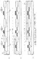
図1において、比較的高抵抗(例えば、n型、10Ωcm程度)の単結晶シリコンから成る基板101に、nウエル102、pウエル103、104を1枚のマスクで自己整合的に形成した。その後、フィールド酸化膜105を形成した。このとき、ボロン(B)を選択的にイオン注入法により基板に導入し、チャネルストッパーを形成しても良い。そして、熱酸化法によりゲート絶縁膜となる酸化シリコン膜106の形成を行った。続いて、ゲート用の多結晶シリコン膜をCVD法により100〜300nmの厚さで形成した。このゲート用の多結晶シリコン膜は、低抵抗化するために予め1021/cm3程度の濃度でリン(P)をドープしておいても良いし、多結晶シリコン膜を形成した後で濃いn型不純物を拡散させても良い。ここでは、さらに低抵抗化するためにこの多結晶シリコン膜上にシリサイド膜を50〜300nmの厚さで形成した。シリサイド材料は、モリブデンシリサイド(MoSix)、タングステンシリサイド(WSix)、タンタルシリサイド(TaSix)、チタンシリサイド(TiSix)などを適用することが可能であり、公知の方法に従い形成すれば良い。そして、この多結晶シリコン膜とシリサイド膜をエッチングしてゲート107〜109を形成した。ゲート107〜109は、多結晶シリコン膜107a〜109aとシリサイド膜107b〜109bの2層構造を有している。(図1(A))
【0019】
次に、nチャネル型FET及びpチャネル型FETに低濃度ドレイン(LDD)領域を形成するために、n型及びp型の導電型を付与する不純物元素を添加した。ここでは、nチャネル型FETに対してリン(P)をイオン注入し、pチャネル型FETに対してボロン(B)をイオン注入した。ドーズ量は1×10¹³/cm2とした。ここではゲートをマスクとしてイオン注入を行い、nチャネル型FETが形成される領域にリン(P)が添加された領域111、112を、pチャネル型FETが形成される領域にボロン(B)が添加された領域115を自己整合的に形成した。(図1(B)、(C))
【0020】
その後、全面にCVD法で酸化シリコン膜や窒化シリコン膜などの絶縁膜を形成し、異方性ドライエッチングでこの膜を全面にわたって均一にエッチングすると、図2(A)に示すように絶縁膜がゲートの側壁に残存させ、サイドウオール116〜118を形成した。このサイドウオールをマスクに用い、nチャネル型FETの領域に砒素を5×10¹⁵/cm2のドーズ量でイオン注入したn型不純物領域(ソースまたはドレイン領域)120、121を形成した。さらに図2(B)に示すように、pチャネル型FETの領域にボロン(B)をイオン注入したp型不純物領域(ソースまたはドレイン領域)124を形成した。
【0021】
そして、n型不純物領域(ソースまたはドレイン領域)120、121およびp型不純物領域(ソースまたはドレイン領域)124上に残存する酸化シリコン膜をエッチング除去して、層間絶縁膜125を全面に形成した。さらにその上にリンガラス(PSG)、あるいはボロンガラス(BSG)、もしくはリンボロンガラス(PBSG)の平坦化膜126を形成した。その後、イオン注入した不純物元素を活性化させるため700〜900℃で熱処理を行った。この熱処理により平坦化膜126がリフローされ、表面がより平坦化された。(図2(C))
【0022】
そして、層間絶縁膜125および平坦化膜126に、n型不純物領域(ソースまたはドレイン領域)120、121およびp型不純物領域(ソースまたはドレイン領域)124に達するコンタクトホールを形成し、ソース配線127、129、131、ドレイン配線128、130、132を形成した。配線に使用する材料に限定はないが、低抵抗材料として通常良く用いられるアルミニウム(Al)を用いると良い。また、Alとチタン(Ti)の積層構造としても良い。
【0023】
この状態で、水素を含む雰囲気中で300〜500℃、好ましくは350〜450℃の熱処理を行うとFETの特性をより好ましい状態にすることができた。
【0024】
この上に形成するパッシベーション膜133は、プラズマCVD法で窒化シリコン膜、または酸化シリコン膜、あるいは窒化酸化シリコン膜で形成した。さらに、有機樹脂絶縁層134を1μm〜2μmの厚さに形成した。有機樹脂材料として、ポリイミド、ポリアミド、アクリル、ベンゾ・シクロ・ブテン(BCB)などを用いることができた。有機樹脂膜を用いることの利点は、膜の形成方法が簡単である点や、比誘電率が低いので寄生容量を低減できる点、平坦化するのに適している点などがある。勿論、上述した以外の有機樹脂膜を用いても良い。ここでは、基板に塗布した後で熱重合するタイプのポリイミドを用い、クリーンオーブンで300℃に加熱し焼成して形成した。
【0025】
さらにこの有機樹脂絶縁層134上に遮光膜135を形成した。遮光膜135はアルミニウム(Al)、チタン(Ti)、タンタル(Ta)から選ばれた元素を含有する膜で形成した。そして画素部に、遮光膜を一方の電極とし、画素電極139を他方の電極とした保持容量を形成するために、遮光膜135上に誘電体層136を形成した。この誘電体層には、公知の成膜法で堆積形成する酸化シリコン膜、窒化シリコン膜、窒酸化シリコン膜やDLC(Diamond like carbon)膜や、上述のポリイミド膜を用いて形成することが可能であるが、陽極酸化法を用いて遮光膜の酸化物層を形成してこれを誘電体層136としても良い。
【0026】
陽極酸化法は、電解溶液中(例えば、3重量%の酒石酸を含有するエチレングリコール溶液中)で、遮光膜を陽極とし、白金を陰極として電圧を印加することにより、緻密でかっピンホールのない誘電体層を形成することができた。誘電体層の厚さは保持容量を形成する目的に対して10〜100nm、好ましくは20〜70nmの厚さで形成すれば良いが、誘電体層の形成に伴って遮光膜の厚さが減少するので、その分を見込んで遮光膜の厚さを確保することが重要であった。
【0027】
表1はAl膜の表面を陽極酸化して50nmの酸化Al膜を形成したときの膜厚の変化と波長550nmの光に対する吸光度の値を示している。吸光度は分光光度計(日立社製U−4000型)で測定した。
【0028】
【表1】
例えば、Al膜の初期膜厚が65nmとして、酸化Al膜を50nm形成すると合計膜厚は80nmに増加したが、Al膜の厚さは30nmに減少した。このとき波長550nmの光に対する吸光度は2.6であった。また、表1のサンプルにおいて、各波長に対する吸光度の特性を図14に示す。図14のデータより300〜600nmの波長範囲で、吸光度はAl膜厚に依存することが明らかとなった。その結果、図14の結果と目視による観察より遮光膜として必要な膜厚は60nm以上、吸光度からみて3.0以上あれば良いと判断することができた。
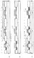
【0030】
陽極酸化法において、陽極と陰極の間に印加する電圧(化成電圧)と、その電極間に流れる電流(化成電流)の制御パターンを図13に示す。図13(A)において、最初化成電流をある一定値に保つように制御して(定電流モード)、予め調べられた誘電体層の生成膜厚に応じた電圧値まで上昇させる。そして、電圧値が所定の値に達した後、その電圧値を保持して(定電圧モード)、電極間に流れる電流がある設定値以下になることをもって陽極酸化の反応が終わったと判断すると、再現性良く同等の膜厚を有する誘電体層を形成することができた。
【0031】
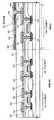
しかしながら、図13(A)の制御パターンで、有機樹脂絶縁膜上に形成した遮光膜の表面に誘電体層を形成した場合、有機樹脂絶縁膜に電解溶液がしみ込んで膨張し、さらに遮光膜と有機樹脂絶縁膜との界面にも電解溶液がしみ込んで、遮光膜の端部から数μmの長さに渡って誘電体層が下地となる有機樹脂絶縁膜側にも形成されてしまった。この様子の一例を図15に示す。図15(A)は、有機樹脂絶縁膜上に形成したAl膜を図13(A)の制御パターンで陽極酸化処理したときの断面構造を、走査電子顕微鏡(SEM)で観察した結果を示す。また、同図(B)はその模式図を示す。同図において、端部における誘電体の厚さをXbとして、端部から誘電体層が下地となる有機樹脂絶縁膜側にも形成される長さをXaとすると、廻り込み量XはXaとXbの差として定義することができる。図15(A)の結果では、廻り込み量Xは約2μmであった。その結果、遮光膜の平坦性が損なわれてしまった。
【0032】
一方、図13(B)に示す化成電圧と化成電流の制御パターンのように、定電流モードとして、その電流密度を図13(A)の条件よりも1.2倍から3倍程度高め、遮光膜の表面に生成される誘電体層の膜厚に応じた所定の電圧まで短時間に急速に上昇させた後、その電圧を保持することなく、或いはその保持時間を極短時間として、陽極酸化を終了させることにより、有機樹脂絶縁膜上で廻り込みのない誘電体層を形成することができた。図16(A)はこのような方法で作製された有機樹脂絶縁膜上の遮光膜とその表面に形成された誘電体層のSEM写真であり、端部からの回り込みが殆どない良好な形状を実現することができた。図16(B)はその模式図を示している。図13(B)のような制御パターンで陽極酸化をしても、緻密でピンホールがなく絶縁耐圧が高い誘電体膜を形成することができた。
【0033】
表2は種々の陽極酸化条件で作製したときの、遮光膜端部からのしみ込み量を評価した結果を示す。端部からのしみ込み量は、電圧の上昇時間と電圧の保持時間と関連が認められ、電圧の上昇時間が短いほど、また、定電圧時間を短くして合計の陽極酸化時間を短縮させることで、しみこみ量を減らすことができた。
【0034】
【表2】
ここでは、図13(B)に示す制御パターンによる陽極酸化法で作製された誘電体層を介して、遮光膜とその一部が重なる画素電極139を形成した。この画素電極139はnチャネル型FET143のドレイン配線に接続している。画素電極は、反射型表示装置とするために、Alに代表される光反射性の材料で形成した。
【0036】
Alは公知の成膜法、例えば真空蒸着法やスパッタ法で容易に形成することができるが、反射型液晶表示装置とする場合、コントラストを良くするために、画素電極の表面を凹凸化して拡散反射面としても良い。
【0037】
以上のようにして、単結晶シリコン基板に、pチャネル型FET141とnチャネル型FET142とから成るCMOS回路を基本とする駆動回路と、nチャネル型FET143と保持容量144が形成された画素部を同一基板上に形成したアクティブマトリクス基板を作製した。CMOS回路を基本とする駆動回路は、CMOS回路を基本として例えば、シフトレジスタ回路、バッファ回路、サンプリング回路、D/Aコンバータ、ラッチ回路などを形成することができる。そしてこのような回路は、単結晶シリコンを活性層とした絶縁ゲート型FETで構成されることにより高速動作が可能であり、また、駆動電圧を3〜5Vとして低消費電力化をすることもできた。
【0038】
また、このような画素部において、遮光膜の表面に密接形成した誘電体膜で保持容量を形成することにより、一画素当たりの画素電極の面積を小さくしても十分な容量を形成することができた。例えば、一画素の面積を400μm2としても約0.5pFの容量を形成することができた。
【0039】
本実施形態で説明したトランジスタの構造はあくまで一実施形態であり、図1〜図3に示した作製工程及び構造に限定される必要はない。本発明で重要な点は、単結晶基板に形成されたFETと、その上に有機樹脂層を介して形成された保持容量の構成にある。
【0040】
[実施形態2]
絶縁物上に単結晶シリコン層(SOI:Silicon On Insulators)を形成したSOI基板として、実施形態1と同様にアクティブマトリクス基板を形成することができる。SOI基板にはその構造や作製方法によっていくつかの種類が知られているが、代表的には、SIMOX(Separation by Implanted Oxygen)、ELTRAN(Epitaxial Layer Transfer:キャノン社の登録商標)基板、Smart-Cut(SOITEC社の登録商標)などを使用することができる。勿論、その他のSOI基板を使用することも可能である。
【0041】
図4はこのようなSOI基板を用いて作製した構成を示す。その作製方法は実施形態1と同様に行えば良く、基板401上に絶縁層402を介して、pチャネル型FET438、nチャネル型FET439を有する駆動回路と、nチャネル型FET440と保持容量441を有する画素部を形成することができる。それぞれのFETはフィールド絶縁膜403で分離されている。
【0042】
駆動回路のpチャネル型FET438には、ゲート407、サイドウオール410、ゲート絶縁膜404、LDD領域413、ソース領域414、ドレイン領域415、ソース配線424、ドレイン配線425が設けられている。nチャネル型FET439には、ゲート408、サイドウオール411、ゲート絶縁膜405、LDD領域416、ソース領域417、ドレイン領域418、ソース配線426、ドレイン配線427が設けられている。また、画素部のnチャネル型FET440には、ゲート409、サイドウオール412、ゲート絶縁膜406、LDD領域419、ソース領域420、ドレイン領域421、ソース配線428、ドレイン配線429が設けられている。
【0043】
層間絶縁膜422は、酸化シリコン膜、窒化シリコン膜、窒化酸化シリコン膜などから形成され、この上にPSGあるいはBSG、もしくはBPSGによる平坦化膜423が形成される。パッシベーション膜430は窒化シリコンまたは窒酸化シリコンで、この平坦化膜423とソース配線424、426、428とドレイン配線425、427、429を覆って形成され、その上に有機樹脂絶縁膜431が形成されている。遮光膜433はアルミニウム(Al)、チタン(Ti)、タンタル(Ta)から選ばれた元素を主成分とする膜で形成した。そしてこの遮光膜433を一方の電極として保持容量を形成する目的で、遮光膜上に誘電体層433を10〜100nm、好ましくは20〜70nmの厚さに形成した。この誘電体層は、陽極酸化法を用いて遮光膜の表面に形成された誘電体層を用いることが望ましい。絶縁膜433を介して遮光膜432上にnチャネル型FET440のドレイン配線429に接続する画素電極436を形成した。ここでは、反射型表示装置とするために、Alに代表される光反射性の材料で形成した。
【0044】
以上のようにして、SOI基板に、pチャネル型トランジスタ438とnチャネル型トランジスタ439とから成るCMOS回路を基本とする駆動回路と、nチャネル型トランジスタ440と保持容量441が形成された画素部を同一基板上に形成することができた。CMOS回路を基本とする駆動回路は、CMOS回路を基本として例えば、シフトレジスタ回路、バッファ回路、サンプリング回路、D/Aコンバータ、ラッチ回路などを形成することができる。
【0045】
[実施形態3]
図5に、画素部に設けられる保持容量の接続方法の他の構成例を示す。図5は実施形態1と同様にして作製された画素部の断面構造を示す。図5(A)において、nチャネル型FET501上には、パッシベーション膜503、有機樹脂からなる層間絶縁膜504が形成され、その上に無機材料から成る膜505が形成されている。この膜は、酸化シリコン膜、窒化シリコン膜、窒酸化シリコン膜などを用いればよく、好ましくはスパッタ法や真空蒸着法で形成すると良い。遮光膜506はこの上に形成され、下地との密着性が改善されるので、絶縁層507を陽極酸化法で形成しても、電解溶液のしみ込みがなくなり、良好な形状を形成できる。そして、パッシベーション膜503および有機樹脂絶縁膜504に設けた開孔508、509により、ドレイン電極502に接続する画素電極510を形成することにより、画素電極510が遮光膜506と重なる領域で保持容量536が形成される。
【0046】
図5(B)において、nチャネル型FET512に接続される保持容量537は、有機樹脂絶縁膜515上に形成された遮光膜516と、その上に形成された誘電体層517と、画素電極522とから形成されている。また、有機樹脂絶縁膜515の開孔が形成される領域には絶縁体のスペーサー518が設けられ、パッシベーション膜514に設けられた開孔519、有機樹脂絶縁膜515に設けられた開孔520、スペーサー518に設けられた開孔521で、画素電極522がドレイン配線513に接続されている。このようにスペーサー518を設けることにより、遮光膜と画素電極との間で発生するショートを確実に防止することができる。保持容量537は遮光膜506、誘電体層517、画素電極522が重なる領域で形成されている。
【0047】
図5(C)はnチャネル型FET524に接続される保持容量538の他の構成について示している。有機樹脂絶縁膜527上に遮光膜528、有機樹脂で形成したスペーサー529を形成が形成される。そして、陽極酸化法で遮光膜516の表面に形成した誘電体層530が形成される。パッシベーション膜526に設けられた開孔531、有機樹脂絶縁膜527に設けられた開孔532、スペーサー529に設けられた開孔533で、画素電極534がドレイン配線525に接続されている。保持容量538は遮光膜516、誘電体層528、画素電極534が重なる部分で形成されている。このような構成とすることで、有機樹脂膜上であってもしみ込みのない陽極酸化膜を形成することができる。
【0048】
【実施例】
[実施例1]
本実例では、実施形態1で作製されたアクティブマトリクス基板から、アクティブマトリクス型液晶表示装置を作製する工程を説明する。図6に示すように、図3の状態の基板に対し、配向膜601を形成する。通常液晶表示素子の配向膜にはポリイミド樹脂が多く用いられている。対向側の基板602には、透明導電膜603と、配向膜604とを形成した。配向膜は形成された後、ラビング処理を施して液晶分子がある一定のプレチルト角を持って平行配向するようにした。そして、画素部と、CMOS回路が形成されたアクティブマトリクス基板と対向基板とを、公知のセル組み工程によってシール材やスペーサ(共に図示せず)などを介して貼りあわせる。その後、両基板の間に液晶材料605を注入し、封止剤(図示せず)によって完全に封止した。
【0049】
上記実施例によって作製された液晶表示装置には、TN液晶以外にも様々な液晶を用いることが可能である。例えば、1998, SID, "Characteristics and Driving Scheme of Polymer-Stabilized Monostable FLCD Exhibiting Fast Response Time and High Contrast Ratio with Gray-Scale Capability" by H. Furue et al.や、1997, SID DIGEST, 841, "A Full-Color Thresholdless Antiferroelectric LCD Exhibiting Wide Viewing Angle with Fast Response Time" by T. Yoshida et al.や、1996, J. Mater. Chem. 6(4), 671-673, "Thresholdless antiferroelectricity in liquid crystals and its application to displays" by S. Inui et al.や、米国特許第5594569 号に開示された液晶を用いることが可能である。
【0050】
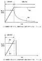
ある温度域において反強誘電相を示す液晶を反強誘電性液晶という。反強誘電性液晶を有する混合液晶には、電場に対して透過率が連続的に変化する電気光学応答特性を示す、無しきい値反強誘電性混合液晶と呼ばれるものがある。この無しきい値反強誘電性混合液晶は、V字型の電気光学応答特性を示すものがあり、その駆動電圧が約±2.5V程度(セル厚約1μm〜2μm)のものも見出されている。
【0051】
ここで、V字型の電気光学応答を示す無しきい値反強誘電性混合液晶の印加電圧に対する光透過率の特性を示す例を図12に示す。図12に示すグラフの縦軸は透過率(任意単位)、横軸は印加電圧である。なお、液晶表示装置の入射側の偏光板の透過軸は、液晶表示装置のラビング方向にほぼ一致する無しきい値反強誘電性混合液晶のスメクティック層の法線方向とほぼ平行に設定されている。また、出射側の偏光板の透過軸は、入射側の偏光板の透過軸に対してほぼ直角(クロスニコル)に設定されている。
【0052】
図12に示されるように、このような無しきい値反強誘電性混合液晶を用いると、低電圧駆動かつ階調表示が可能となることがわかる。
【0053】
このような低電圧駆動の無しきい値反強誘電性混合液晶をアナログドライバを有する液晶表示装置に用いた場合には、画像信号のサンプリング回路の電源電圧を、例えば、5V〜8V程度に抑えることが可能となる。よって、ドライバの動作電源電圧を下げることができ、液晶表示装置の低消費電力化および高信頼性が実現できる。
【0054】
また、このような低電圧駆動の無しきい値反強誘電性混合液晶をデジタルドライバを有する液晶表示装置に用いた場合にも、D/A変換回路の出力電圧を下げることができるので、D/A変換回路の動作電源電圧を下げることができ、ドライバの動作電源電圧を低くすることができる。よって、液晶表示装置の低消費電力化および高信頼性が実現できる。
【0055】
よって、このような低電圧駆動の無しきい値反強誘電性混合液晶を用いることは、比較的LDD領域(低濃度不純物領域)の幅が小さなTFT(例えば、0nm〜500nmまたは0nm〜200nm)を用いる場合においても有効である。
【0056】
また、一般に、無しきい値反強誘電性混合液晶は自発分極が大きく、液晶自体の誘電率が高い。このため、無しきい値反強誘電性混合液晶を液晶表示装置に用いる場合には、画素に比較的大きな保持容量が必要となってくる。よって、自発分極が小さな無しきい値反強誘電性混合液晶を用いるのが好ましい。また、液晶表示装置の駆動方法を線順次駆動とすることにより、画素への階調電圧の書き込み期間(ピクセルフィードピリオド)を長くし、保持容量が小くてもそれを補うようにしてもよい。
【0057】
なお、このような無しきい値反強誘電性混合液晶を用いることによって低電圧駆動が実現されるので、本発明のアクティブマトリクス基板で液晶表示装置を形成すると低消費電力が実現される。
【0058】
なお、図12に示すような電気光学特性を有する液晶であれば、いかなるものも本発明の液晶表示装置の表示媒体として用いることができる。
【0059】
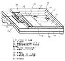
次にこのアクティブマトリクス型液晶表示装置の構成を、図7の斜視図および図8の上面図を用いて説明する。尚、図7と図8は、図1〜図3および図6の断面構造図と対応付けるため、共通の符号を用いている。アクティブマトリクス基板は、基板101上に形成された、画素部701と、走査(ゲート)線駆動回路702と、信号(ソース)線駆動回路703で構成される。画素部のnチャネル型トランジスタ143、周辺に設けられる駆動回路はCMOS回路を基本として構成されている。走査(ゲート)線駆動回路702と、信号(ソース)線駆動回路703はそれぞれゲート配線109とソース配線131で画素部701に接続されている。また、FPC731は外部入出力端子734に接続されている。また、基板101は樹脂層735を介してベース板736に固定され、機械的強度を保持すると共に、ベース板736を熱伝導性の良い材料で形成することで、放熱効果をもたせることもできた。
【0060】
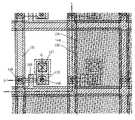
図8は画素部701の一部分を示す上面図である。ゲート電極109は、図示されていないゲート絶縁膜を介して単結晶シリコン上に形成されている。図示はしていないが、単結晶シリコンには、ソース領域、ドレイン領域、が形成されている。また、この上には遮光膜135と、誘電体層(図示せず)と、各画素ごとに設けられる画素電極139が形成され、遮光膜135と画素電極139とが誘電体層を介して重なる領域で保持容量143が形成される。誘電体層を容量部を形成するための誘電体膜としたことで、必要な容量を形成するための面積を少なくすることが可能であり、さらに、本実施例のように画素TFT上に形成される遮光膜を保持容量の一方の電極とすることで、アクティブマトリクス型液晶表示装置の画像表示部の開口率を向上させることができた。また、図8で示すA―A’に沿った断面構造は、図3に示す画素部のA―A’断面図に対応している。
【0061】
このようにして作製された反射型液晶表示装置は、直視型の表示装置とした電気光学装置の他に、投影型の表示装置とした電気光学装置にも利用できる。
【0062】
[実施例2]
本実施例では、本発明を表示装置として用いた電気光学装置の一例について説明する。実施例1に示した反射型の表示装置を三板式投影装置に適用した場合について図9を用いて説明する。
【0063】
図9において、メタルハライドランプ、ハロゲンランプなどからなる光源901から放射された光は、偏光ビームスプリッター902で反射され、クロスダイクロイックミラー903に進む。尚、偏光ビームスプリッターとは光の偏光方向によって反射したり透過したりする機能を有した光学フィルターである。この場合、光源901からの光は偏光ビームスプリッター902で反射されるような偏光を与えてある。
【0064】
この時、クロスダイクロイックミラー903では、赤(R)に対応する液晶表示装置904の方向に赤(R)成分光が反射され、青(B)に対応する液晶表示装置906の方向に青(B)成分光が反射される。また、緑(G)成分光はクロスダイクロイックミラー903を透過して、緑(G)に対応する液晶表示装置905に入射する。各色に対応した液晶表示装置904〜906は、画素がオフ状態にある時は入射光の偏光方向を変化させないで反射するように液晶分子を配向している。また、画素がオン状態にある時は液晶層の配向状態が変化し、入射光の偏光方向もそれに伴って変化するように構成されている。
【0065】
これらの液晶表示装置904〜906で反射された光は再びクロスダイクロイックミラー903で反射(緑(G)成分光は透過)して合成され、再び偏光ビームスプリッタ902へと入射する。この時、オン状態にある画素領域で反射された光は偏光方向が変化するため偏光ビームスプリッタ902を透過する。一方、オフ状態にある画素領域で反射された光は偏光方向が変化しないため偏光ビームスプリッタ902で反射される。このように、画素部にマトリクス状に配置された画素領域を複数のトランジスタでオン・オフ制御することによって特定の画素領域で反射された光のみが偏光ビームスプリッタ902を透過できるようになる。この動作は各液晶表示装置904〜906で共通である。
【0066】
以上のようにして偏光ビームスプリッタ902を透過した画像情報を含む光は投影レンズ等で構成される光学系レンズ907でスクリーン908に映し出される。ここでは、基本的な構成について示したが、このような原理を応用して投影型の電気光学装置を実現することができる。
【0067】
[実施例3]
本実施例では、本発明をアクティブマトリクス型EL表示装置に適用した例を図10と図11で説明する。図10(A)はアクティブマトリクス型EL表示装置の回路図を示す。このEL表示装置は、基板上に設けられた表示領域11、X方向周辺駆動回路12、Y方向周辺駆動回路13から成る。この表示領域11は、スイッチ用トランジスタ330、保持容量332、電流制御用トランジスタ331、有機EL素子333、X方向信号線18a、18b、電源線19a、19b、Y方向信号線20a、20b、20cなどにより構成される。
【0068】
図10(B)はほぼ一画素分の上面図を示している。同図において、B−B‘に沿った断面構造を図11に示す。図11の断面構造は単結晶シリコン基板を用いた構成例を示すが、このような構成はSOI基板を用いても同様に実現できる。基板301にnウエル302、pウエル303が形成され、隣接するFETを分離するためフィールド酸化膜304が形成される。スイッチ用FET330はpチャネル型FETで形成され、ゲート絶縁膜305、ゲート307、サイドウオール309、LDD領域311、ソース領域312、ドレイン領域313、ソース配線318、ドレイン配線319を有している。また、電流制御用トランジスタ331はnチャネル型FETで、ゲート絶縁膜306、ゲート308、サイドウオール310、LDD領域314、ソース領域315、ドレイン領域316、ソース配線320、ドレイン配線321を有している。保持容量332は、層間絶縁膜322上に形成され、スイッチ用FET330のドレイン配線319に接続する容量電極323と、電源線19aとの間に設けられた誘電体層324とから形成される。ここで、容量電極323をAl、Ta、Tiから選ばれた元素を主成分とする材料で形成し、その表面を陽極酸化して誘電体層324を形成すれば、良好な保持容量を形成できる。有機EL素子333は層間絶縁膜326を介して形成され、電流制御用FET331のドレイン配線321に接続するEL素子下部電極327、有機EL層328、EL素子上部電極329から形成される。
【0069】
ここでは、EL表示装置の画素領域の構成について示したが、実施例1と同様に画素領域の周辺に駆動回路を設けた周辺回路一体型のアクティブマトリクス型表示装置とすることもできる。そして、図示しないがカラーフィルターを設ければカラー表示をすることも可能であった。
【0070】
[実施例4]
本実施例では、本発明のTFT回路によるアクティブマトリクス型液晶表示装置を組み込んだ半導体装置について図17、図23で説明する。図17、図23に示す半導体装置は、本発明の実施形態や実施例で示したアクティブマトリクス型表示装置を好適に用いることができる。
【0071】
このような半導体装置には、携帯情報端末(電子手帳、モバイルコンピュータ、携帯電話等)、ビデオカメラ、デジタルスチルカメラ、パーソナルコンピュータ、テレビ等が挙げられる。それらの一例を図17に示す。
【0072】
図17(A)は携帯電話であり、本体9001、音声出力部9002、音声入力部9003、表示装置9004、操作スイッチ9005、アンテナ9006から構成されている。本願発明は音声出力部9002、音声入力部9003、及び画素部を備えた表示装置9004に適用することができる。
【0073】
図17(B)はビデオカメラであり、本体9101、表示装置9102、音声入力部9103、操作スイッチ9104、バッテリー9105、受像部9106から成っている。本願発明は音声入力部9103、及び画素部を備えた表示装置9102、受像部9106に適用することができる。
【0074】
図17(C)はモバイルコンピュータであり、本体9201、カメラ部9202、受像部9203、操作スイッチ9204、表示装置9205で構成されている。本願発明は受像部9203、及び画素部を備えた表示装置9205に適用することができる。
【0075】
図17(D)はゴーグル型ディスプレイであり、本体9301、表示装置9302、アーム部9303で構成される。本願発明は表示装置9302に適用することができる。また、表示されていないが、その他の信号制御用回路に使用することもできる。
【0076】
図17(E)はリア型プロジェクターであり、本体9401、光源9402、表示装置9403、偏光ビームスプリッタ9404、リフレクター9405、9406、スクリーン9407で構成される。本発明は表示装置9403に適用することができる。
【0077】
図17(F)は携帯書籍であり、本体9501、表示装置9502、9503、記憶媒体9504、操作スイッチ9505、アンテナ9506から構成されており、ミニディスク(MD)やDVDに記憶されたデータや、アンテナで受信したデータを表示するものである。表示装置9502、9503は直視型の表示装置9502、9503であり、本発明はこの表示装置9502、9503に適用することができる。
【0078】
図23(A)はプログラムを記録した記録媒体(以下、記録媒体と呼ぶ)を用いるプレーヤーであり、本体9701、表示装置9702、スピーカ部9703、記録媒体9704、操作スイッチ9705で構成される。なお、この装置は記録媒体としてDVD(Digtial Versatile Disc)、CD等を用い、音楽鑑賞や映画鑑賞やゲームやインターネットを行うことができる。本発明を用いて作製される液晶表示装置やEL表示装置は表示装置9702に適用することができる。
【0079】
図23(B)はデジタルカメラであり、本体9801、表示装置9802、接眼部9803、操作スイッチ9804、受像部(図示しない)で構成される。本発明で作製される液晶表示装置やEL表示装置は表示装置9802に適用することができる。
【0080】
また、ここでは図示しなかったが、本発明はその他にも、カーナビゲーションシステムやイメージセンサ、パーソナルコンピュータの表示部に適用することも可能である。このように、本願発明の適用範囲はきわめて広く、あらゆる分野の電子機器に適用することが可能である。
【0081】
[実施例5]
単結晶半導体基板を用いたアクティブマトリックス型の表示装置は、LSIやVLSIなどの集積回路の製造技術をそのまま応用することができるので、小型で高精細の表示装置を作製することができる。例えば、画面サイズが1型(対角2.56cm)程度のものでもVGAクラス(画素数640×480)の表示装置を実現することができる。
【0082】
しかし、素子の集積度の向上と共に素子面積や配線の幅などが小さくなるので、回路の性能を維持するために、拡散層や配線に用いる多結晶シリコン膜の抵抗を下げることが必要となる。この目的を解決する方法の一つに自己整合シリサイド(Self-Aligned Silicde:サリサイドと呼ばれる)を用いる技術が知られている。これは、基板上にチタン(Ti)などの金属層を形成し、加熱処理によりシリコンが露出している領域に自己整合的にシリサイドを形成する方法である。
【0083】
本実施例では、サリサイド技術を用いてアクティブマトリックス型の表示装置を作製する例について図18〜図20を用いて説明する。
【0084】
図18(A)において、基板201は実施形態1と同様なものを用い、nウエル202、pウエル203、204を1枚のマスクで自己整合的に形成し、さらにフィールド酸化膜205を形成する。そして、熱酸化法によりゲート絶縁膜となる酸化シリコン膜206の形成を行う。ゲート207〜209は、リンに代表されるn型不純物を高濃度に添加した多結晶シリコン膜で形成する。
【0085】
次に図18(B)と(C)に示すように、nチャネル型FET及びpチャネル型FETに低濃度ドレイン(LDD)領域を形成するために、n型及びp型の導電型を付与する不純物元素を添加する。これは、イオンドープ法で行っても良いし、イオン注入法で行っても良い。nチャネル型FETに対してリン(P)をイオン注入し、pチャネル型FETに対してボロン(B)をイオン注入する。ドーズ量は1×10¹³/cm2とする。ゲートをマスクとしてイオン注入を行い、nチャネル型FETが形成される領域にリン(P)が添加されるn型不純物領域211、212を、pチャネル型FETが形成される領域にボロン(B)が添加されるp型不純物領域215が自己整合的に形成することができる。
【0086】
その後、全面CVD法で酸化シリコン膜や窒化シリコン膜などの絶縁膜を形成し、異方性ドライエッチングでこの膜をエッチングして図19(A)に示すようにゲート207〜209の側壁にサイドウオール216〜218を形成する。そして、レジストマスク219を形成し、pチャネル型FETを形成する領域にボロン(B)をイオン注入し、p型不純物領域220を形成する。p型不純物領域220は加速電圧を50〜100keVとしてp型不純物領域215よりも深くなるように形成する。
【0087】
図19(B)に示すように、レジストマスク219を除去した後、Ti、Mo、Crなどの金属221を全面に形成する。代表的にはTiが用いられ、スパッタ法で50〜1000nmの厚さで全面に形成する。その後、600〜800℃、好ましくは650〜750℃で熱処理を行いチタンシリサイドを形成する。チタンシリサイドはTi膜とシリコンとが接触する部分で自己整合的に形成され、熱処理後に残ったTi膜を選択的にエッチングすることで図19(C)で示すようにチタンシリサイド層223〜228は多結晶シリコン膜で形成したゲート上とp型及びn型不純物領域上に形成される。しかし、800℃以下の温度で形成されたチタンシリサイド膜は高抵抗相が形成される。これを900℃程度で5〜120秒程度の熱処理を行うことにより低抵抗相が形成される。この熱処理はファーネスアニール炉で行っても良いが、フラッシュランプアニール法を用いても良い。チタンシリサイドを形成することでゲート及び、p型またはn型不純物領のシート抵抗は2〜4Ω/□を得ることができる。
【0088】
そして、pチャネル型FETを形成する領域にレジストマスク229を形成し、サイドウオールとゲートをマスクとしてnチャネル型FETの領域に加速電圧を50〜120keVとして砒素を5×10¹⁵/cm2のドーズ量で注入し、n型不純物領域230、231を形成する。この不純物領域もn型不純物領域211、212よりも深く形成する。
【0089】
そして図20に示すように、層間絶縁膜232、リンガラス(PSG)、ボロンガラス(BSG)、またはリンボロンガラス(PBSG)から成る平坦化膜233を形成する。その後、イオン注入した不純物元素を活性化させるため700〜900℃で熱処理を行う。この熱処理により平坦化膜233がリフローされ、表面の平坦性を向上させることができる。
【0090】
そして、層間絶縁膜232および平坦化膜233にコンタクトホールを形成し、ソースまたはドレイン配線234〜239をAlやTiとAlの積層膜などで形成する。この状態で、水素を含む雰囲気中で300〜500℃、好ましくは350〜450℃の熱処理を行うとFETの特性をより好ましい状態にすることができる。
【0091】
この上に形成するパッシベーション膜240は窒化シリコン膜、または酸化シリコン膜、あるいは窒化酸化シリコン膜などで50〜200nm程度の厚さで形成し、さらに有機樹脂絶縁層241を1μm〜2μmの厚さで形成する。さらにこの有機樹脂絶縁層241上に遮光膜242をAlで形成し、その表面を実施形態1と同様にして陽極酸化法を用いて酸化して誘電体層243を形成する。その上に画素電極246、247をAlに代表される光反射性の材料で形成する。
【0092】
以上のようにして、サリサイド技術を用いて単結晶シリコン基板に、pチャネル型FET248とnチャネル型FET249とから成る駆動回路部と、nチャネル型FE250と保持容量251が形成された画素部を同一基板上に形成したアクティブマトリクス基板を形成することができる。保持容量は遮光膜242、誘電体膜243、画素電極246が重なる領域で形成され、遮光膜として用いたAlの表面に形成された酸化膜は誘電率が高く、50〜100nmの厚さで形成することで、一画素当たりの画素電極の面積を小さくしても画素部の駆動に必要な容量を形成することができる。例えば、一画素の面積を400μm2としても約0.5pFの容量を形成することができる。
【0093】
駆動回路部はCMOS回路を基本として形成され、シフトレジスタ回路、バッファ回路、サンプリング回路、D/Aコンバータ、ラッチ回路などを形成することができる。そしてこのような回路は、単結晶シリコンを活性層とした絶縁ゲート型FETで構成されることにより高速動作が可能であり、また、駆動電圧を3〜5Vとして低消費電力化をすることもできる。
【0094】
また、p型不純物領域215、n型不純物領域211、212はLDD領域となり、ホットキャリア効果などによるFETの劣化を防止することができる。
【0095】
また、サリサイド技術を用いることにより、ゲート配線の低抵抗化をすることができ、配線遅延の問題を低減することができ、さらにソースまたはドレイン領域の低抵抗化によりFETの動作特性を向上させることができる。以上のような効果により、小型で高精細なアクティブマトリックス型の表示装置を実現することができる。
【0096】
本実施例で説明したトランジスタの構造はあくまで一実施形態であり、図18〜図20に示した作製工程及び構造に限定される必要はない。本発明で重要な点は、単結晶基板に形成されたFETと、その上に有機樹脂層を介して形成された保持容量の構成にある。
【0097】
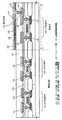
[実施例6]
本実施例ではアクティブマトリクス型EL表示装置の他の実施例を図21と図22を用いて説明する。駆動回路部と画素部が形成されたアクティブマトリックス基板は実施形態1と同様にして作製する。
【0098】
基板801にはnウエル802、pウエル803〜805が自己整合的に形成され、フィールド酸化膜806で分離されている。ゲート絶縁膜810、816、822、828は熱酸化法により形成したものである。ゲート811、817、823、829は多結晶シリコン膜をCVD法により100〜300nmの厚さで形成した多結晶シリコン層811a、817a、823a、829aと、その上に50〜300nmの厚さで形成したシリサイド層811b、817b、823b、829bから成っている。
【0099】
pチャネル型FET881の低濃度ドレイン(LDD)領域807にはp型の導電型を付与する不純物元素としてボロン(B)がドーズ量で1×10¹³〜1×10¹⁴/cm2添加されている。一方、nチャネル型FET882とnチャネル型FETで作製されるスイッチングFET883、電流制御FET884のLDD領域813、819、825にはn型の導電型を付与する不純物元素としてリン(P)または砒素(As)がやはり同様のドーズ量で添加されている。これらのLDD領域はゲートをマスクとしてイオン注入法またはイオンドープ法で自己整合的に形成されている。
【0100】
サイドウオール812、818、824、830はLDD領域を形成後、全面にCVD法で酸化シリコン膜や窒化シリコン膜などの絶縁膜を形成し、異方性ドライエッチングでこの膜を全面にわたって均一にエッチングし、ゲートの側壁に絶縁膜を残存させて形成したものである。各FETのソース領域およびドレイン領域はこのサイドウオールをマスクに用い形成したものである。pチャネル型FET881には、ボロン(B)を5×10¹⁴〜1×10¹⁶/cm2のドーズ量でイオン注入したソース領域808、ドレイン領域809が形成されている。nチャネル型FET882nチャネル型FETで作製されるスイッチングFET883、電流制御FET884には、それぞれ砒素(As)を5×1014〜1×1016/cm2のドーズ量でイオン注入したソース領域814、820、826とドレイン領域815、821、827が形成されている。
【0101】
第1の層間絶縁膜831は好適にはプラズマCVD法や減圧CVD法で作製される酸化シリコン膜や酸化窒化シリコン膜などで100〜2000nmの厚さ形成する。さらにその上にリンガラス(PSG)、あるいはボロンガラス(BSG)、もしくはリンボロンガラス(PBSG)の第2の層間絶縁膜832が形成されている。第2の層間絶縁膜832はスピンコート法や常圧CVD法で作製されるもので、形成後実施される700〜900℃の熱処理を兼ねた熱活性化の処理により第2の層間絶縁膜832がリフローされ表面が平坦化される。
【0102】
ソース配線833、835、837、839及びドレイン配線834、836、838、840は、第1の層間絶縁膜831および平坦化膜832にそれぞれのFETのソース領域及びドレイン領域に達するコンタクトホールを形成した後形成されるもので、低抵抗材料として通常良く用いられるAlを用いると良い。また、AlとTiの積層構造としても良い。
【0103】
パッシベーション膜841は、プラズマCVD法で窒化シリコン膜、または酸化シリコン膜、あるいは窒化酸化シリコン膜で形成されている。さらに、第3の層間絶縁膜を842は有機樹脂材料で1μm〜2μmの厚さに形成されている。画素電極843は電流制御FET884のドレイン配線に接続している。画素電極は、Alに代表される低抵抗の材料で形成する。
【0104】
画素電極843まで形成したら、全ての画素電極の上に仕事関数の低い金属を含む陰極層844が形成される。これは数nm程度と膜厚が薄いため層状に形成されているのか島状に点在しているのか不明のため、輪郭を点線で示している。
【0105】
上記仕事関数の低い金属を含む陰極層の材料としては、フッ化リチウム(LiF)、酸化リチウム(Li2O)、フッ化バリウム(BaF2)、酸化バリウム(BaO)、フッ化カルシウム(CaF2)、酸化カルシウム(CaO)、酸化ストロンチウム(SrO)または酸化セシウム(Cs2O)を用いることができる。これらは絶縁性であるため、層状に形成されたとしても画素電極間のショート(短絡)を招くようなことはない。勿論、MgAg電極のような公知の導電性を有する材料を陰極層として用いることも可能であるが、画素電極同士が短絡しないように、陰極自体を選択的に設けるか、パターニングを行う必要がある。
【0106】
仕事関数の低い金属を含む陰極層844の上に有機EL層(エレクトロルミネッセンス層)845が形成される。有機EL層845は公知の材料や構造を用いることができるが本願発明では白色発光の可能な材料を用いる。構造としては、再結合の場を提供する発光層だけで有機EL層としても良いし、必要に応じて電子注入層、電子輸送層、正孔輸送層、電子阻止層、正孔阻止層もしくは正孔注入層を積層しても良い。本明細書中では、キャリアの注入、輸送または再結合が行われる層をすべて含めて有機EL層と呼ぶ。
【0107】
また、有機EL層845として用いる有機EL材料はポリマー系の高分子系有機EL材料を用いる。有機EL層845は、PVK(ポリビニルカルバゾール)、Bu−PBD(2−(4'−tert−ブチルフェニル)−5−(4''−ビフェニル)−1,3,4−オキサジアゾール)、クマリン6、DCM1(4−ジシアノメチレン−2−メチル−6−p−ジメチルアミノスチリル−4H−ピラン)、TPB(テトラフェニルブタジエン)、ナイルレッドを1,2−ジクロロメタンまたはクロロホルムに溶解し、スピンコート法により塗布する。回転数は500〜1000rpm程度とし、20〜60秒間回転させ均一な塗布膜を形成する。
【0108】
勿論、上記有機EL材料は少なくとも3回以上、好ましくは5回以上の精製(典型的には透析法)を施し、含まれるナトリウム濃度を0.1ppm以下(好ましくは0.01ppm以下)にしてから成膜する。こうすることで図21に示す有機EL層845中に含まれるナトリウム濃度は0.1ppm以下(好ましくは0.01ppm以下)となり、体積抵抗値は1×10¹¹〜1×10¹²Ωcm(好ましくは1×10¹²〜1×10¹³Ωcm)となる。
【0109】
このようにして形成された有機EL層845の上には、陽極層846として透明導電膜が形成される。透明導電膜としては、酸化インジウムと酸化スズとの化合物(ITOと呼ばれる)、酸化インジウムと酸化亜鉛との化合物、酸化スズ(SnO2)または酸化亜鉛(ZnO)などを用いることが可能である。
【0110】
また、陽極層846の上にはパッシベーション膜847として絶縁膜が設けられる。パッシベーション膜847としては、窒化珪素膜、窒化酸化珪素膜(SiOxNyで表される)を用いることが好ましい。
【0111】
図22(A)はアクティブマトリックス型EL表示装置の画素部の上面図であり、図22(B)はその回路構成である。実際には画素がマトリクス状に複数配列されて画素部(画像表示部)が形成される。なお、図22(A)をA−A’で切断した断面図が図21の画素部の断面図に相当する。従って図21及び図22で共通の符号を用いているので、適宜両図面を参照すると良い。また、図22(A)の上面図では二つの画素を図示しているが、どちらも同じ構造である。図22(B)に示すように、有機EL素子885には、一画素当たり2つのFETが設けられる。いずれもnチャネル型FETであり、スイッチング用FET883と電流制御用FET884として機能している。
【0112】
以上のようにして、単結晶シリコン基板に、pチャネル型FET881とnチャネル型FET882とから成るCMOS回路を基本とする駆動回路と、nチャネル型FETで形成されるスイッチング用FET883と電流制御用FET884とを備えた画素部が形成することができる。CMOS回路を基本とする駆動回路は、CMOS回路を基本として例えば、シフトレジスタ回路、バッファ回路、サンプリング回路、D/Aコンバータ、ラッチ回路などを形成することができる。そしてこのような回路は、単結晶シリコンを活性層とした絶縁ゲート型FETで構成されることにより高速動作が可能であり、また、駆動電圧を3〜5Vとして低消費電力化をすることもできる。尚、本実施形態で説明したFETの構造はあくまで一実施形態であり、図21に示した構造に限定される必要はない。
【0113】
【発明の効果】
本発明により得られる代表的な効果を簡単に説明すれば下記のとおりである。
【0114】
単結晶シリコンに代表される単結晶半導体を活性層としたFETで画素部と、その画素部に接続する駆動回路を同一基板上に設けたアクティブマトリクス基板において、FET上に有機樹脂絶縁層を形成し、その上に形成した遮光膜と、遮光膜に密接形成した誘電体層と、遮光膜とその一部が重なるように設けられた画素電極とで保持容量を形成することにより、低消費電力で高速動作が可能で高信頼性の表示装置を形成できる。
【0115】
このようなアクティブマトリクス基板で、無しきい値反強誘電性混合液晶を用いた液晶表示装置に好適に用いることができる。
【0116】
上記表示装置において、遮光膜に密接する誘電体層を陽極酸化法で形成することにより、ピンホールなどの欠陥のない良質な誘電体層を形成することが可能となる。また陽極酸化法で誘電率の高い誘電体層を薄く均一に形成することにより、画素ピッチを縮小させても十分な保持容量を確保することができる。
【0117】
有機樹脂絶縁層上に設けた遮光膜に密接する誘電体層を陽極酸化法で形成する方法において、図13(B)で示した化成電圧と化成電流との制御パターンで行うことにより、端部からのしみ込みがない誘電体層を形成することができる。このように作製した誘電体層で保持容量を形成することにより信頼性の高い表示装置を実現できる。
【図面の簡単な説明】
【図1】 画素部、ロジック回路の作製工程を示す断面図。
【図2】 画素部、ロジック回路の作製工程を示す断面図。
【図3】 画素部、ロジック回路の作製工程を示す断面図。
【図4】 画素部、ロジック回路の断面図。
【図5】 保持容量の構成を説明する断面図。
【図6】 アクティブマトリクス型液晶表示装置の断面図。
【図7】 アクティブマトリクス型液晶表示装置の斜視図。
【図8】 画素部の上面図。
【図9】 反射型液晶表示装置を用いたプロジェクタの構成を示す図。
【図10】 EL表示装置の回路図と上面図。
【図11】 EL表示装置の断面図。
【図12】 無しきい値反強誘電性混合液晶の印加電圧と透過率の特性を示す図。
【図13】 陽極酸化方法を示す化成電圧および電流の制御パターン図。
【図14】 遮光膜の吸光度特性を示す図。
【図15】 有機樹脂絶縁層上のAl膜を陽極酸化処理したときの断面SEM像
【図16】 有機樹脂絶縁層上のAl膜を陽極酸化処理したときの断面SEM像
【図17】 半導体装置の一例を示す図。
【図18】 画素部、ロジック回路の作製工程を示す断面図。
【図19】 画素部、ロジック回路の作製工程を示す断面図。
【図20】 画素部、ロジック回路の作製工程を示す断面図。
【図21】 アクティブマトリックス型EL表示装置の断面図。
【図22】 EL表示装置の画素部の上面図及び回路図。
【図23】 半導体装置の一例を示す図。[0001]
BACKGROUND OF THE INVENTION
The present invention relates to a semiconductor device having an integrated circuit using an insulated gate field effect transistor having a single crystal semiconductor as an active layer, and a method for manufacturing the semiconductor device. In particular, the present invention relates to a liquid crystal display device or an electro-optic (EL) display device in which a pixel portion (active matrix circuit) and a drive circuit connected to the pixel portion are provided on the same substrate. The present invention can be suitably used for an apparatus and an electronic apparatus equipped with an electro-optical device. Note that in this specification, a semiconductor device refers to all devices that function by utilizing semiconductor characteristics, and includes the above-described electro-optical device and electronic equipment including the electro-optical device in its category.
[0002]
[Prior art]
In a flat panel display represented by a liquid crystal display device, an EL display device, or the like, an insulated gate field effect transistor (hereinafter referred to as a FET) is formed on a single crystal semiconductor substrate. A technique for manufacturing an active matrix display device is known. This is different from the case where an active matrix type display device is manufactured by forming a thin film transistor (hereinafter referred to as TFT) on a glass substrate or a quartz substrate, and the technology cultivated in a large scale integrated circuit (LSI) is applied as it is. Therefore, there is an advantage in that high-performance FETs that can be driven at a high speed and a low voltage can be integrally formed on a substrate at a high density. However, on the other hand, since the substrate is opaque to visible light, it is limited to a reflective type or a self-luminous type display device, or a single crystal semiconductor substrate is limited to a size supplied in the market. Was considered a drawback.
[0003]
However, in the technical orientation such as high image quality and full digitalization in the field of display devices, performance improvements required for active matrix display devices are inevitably increasing. In a pixel portion that performs image display in an active matrix display device, tens to millions of transistors (TFTs, FETs, and the like) are arranged, and a pixel electrode is connected to each of the transistors. It was. Then, the voltage applied to each pixel is controlled by the switching function of the transistor, and the liquid crystal is driven or the EL element emits light to display an image. For example, in the case of a liquid crystal display device, a counter electrode is provided on the side of the counter substrate sandwiching the liquid crystal, and a kind of capacitor using liquid crystal as a dielectric (referred to as a liquid crystal capacitor in this specification) is formed. . The liquid crystal was driven by controlling the charge accumulated in the liquid crystal capacitance, and the amount of light transmitted through the liquid crystal was controlled to display an image. However, since the capacitance of the liquid crystal capacitance is gradually reduced due to a leak current, the amount of transmitted light is changed, which causes a decrease in image display contrast. Therefore, it is necessary to provide each pixel with a capacitor (hereinafter referred to as a storage capacitor) different from the liquid crystal capacitor. This holding capacitor serves to compensate for the loss of the liquid crystal capacitance, and is provided for holding charges during a period of one frame from writing to the next writing. Further, in the EL display device, when the switching transistor provided in each pixel is turned on, a current flows through the current control transistor by a signal corresponding to the image data, and the EL element emits light by itself. .
[0004]
[Problems to be solved by the invention]
In such an active matrix type display device, it is expected that a digital method will become the mainstream in order to realize further higher definition and higher density of image information in the future. Therefore, it is necessary to newly provide a circuit necessary for processing a digital signal such as a D / A converter and a latch circuit, and the configuration of the drive circuit is more complicated than that of the conventional analog system, and high speed operation is possible. It has been a problem to form a display device with a driver circuit using a transistor. However, TFTs formed on glass or quartz substrates have an electron mobility of 400 cm that can be achieved even when polycrystalline silicon is used for the active layer.2 / V · sec, about 1/3 that of an FET made of single crystal silicon.
[0005]
Further, when the pixel density is increased, the area of the pixel electrode per pixel is reduced, and the ratio of the wiring and the transistor is inevitably increased, thereby decreasing the aperture ratio. Further, as the area of the pixel electrode is reduced, the area where the storage capacitor can be formed is also reduced, so that it is difficult to form a capacitor necessary for driving the pixel portion with a limited area. It was.
[0006]
The present invention solves the above-mentioned problems, and a display device is formed by a drive circuit using an insulated gate FET capable of high-speed operation, and sufficient storage capacity can be obtained even if the area of the pixel electrode per unit pixel is reduced. An active matrix display device is obtained. It is another object of the present invention to provide an active matrix liquid crystal display device with low power consumption and high reliability.
[0007]
[Means for Solving the Problems]
In order to solve the above problems, the configuration of the present invention is a semiconductor device including a pixel portion using an insulated gate field effect transistor having a single crystal semiconductor as an active layer, and an organic resin insulating layer on the insulated gate field effect transistor. A light shielding layer formed on the organic resin insulating layer, a dielectric layer formed in close contact with the light shielding layer, and a light reflective electrode connected to the insulated gate field effect transistor. A storage capacitor is formed.
[0008]
Another structure of the present invention is a semiconductor device in which a liquid crystal is sandwiched between a pair of substrates, and one substrate includes an insulated gate field effect transistor having a single crystal semiconductor as an active layer, and the insulated gate field. An organic resin insulating layer is formed on the effect transistor, a light shielding layer formed on the organic resin insulating layer, a dielectric layer formed in close contact with the light shielding layer, and connected to the insulated gate field effect transistor A storage capacitor is formed from the light-reflecting electrode, and at least a light-transmitting conductive film is formed on the other substrate.
[0009]
Another structure of the present invention is an organic resin insulating layer formed on the insulated gate field effect transistor in a semiconductor device comprising an insulated gate field effect transistor having an active layer of a single crystal semiconductor and an organic EL element. A storage capacitor comprising: a light shielding layer formed on the organic resin insulating layer; a dielectric layer formed in close contact with the light shielding layer; and a light reflective electrode connected to the insulated gate field effect transistor. It is characterized by being formed.
[0010]
In the present invention, an insulating layer made of an inorganic compound is formed between the organic resin insulating layer and the light shielding layer, or on the surface of the organic resin insulating layer on the side where the light shielding layer is formed. Alternatively, a structure in which an insulating layer made of an inorganic compound is formed may be employed.
[0011]
In the present invention, it is preferable that the light shielding layer is made of a material containing one kind or plural kinds selected from aluminum, tantalum, and titanium, and the dielectric layer is an oxide of the material.
[0012]
According to the structure of the present invention, an organic resin layer is formed on the insulated gate field effect transistor in a method for manufacturing a semiconductor device including a pixel portion using an insulated gate field effect transistor having a single crystal semiconductor as an active layer. Forming a light-shielding layer on the organic resin; forming an insulating layer in close contact with the light-shielding layer; and forming a light-reflective electrode having a region overlapping the light-shielding layer via the insulating layer And a step of performing.
[0013]
Another structure of the present invention is a method for manufacturing a semiconductor device in which a liquid crystal is sandwiched between a pair of substrates, a step of forming an insulated gate field effect transistor using a single crystal semiconductor as an active layer on one substrate; Forming an organic resin layer on the insulated gate field effect transistor; forming a light shielding layer on the organic resin layer; forming an insulating layer in close contact with the light shielding layer; and the insulated gate. A step of forming a light-reflective electrode connected to the p-type field effect transistor, and a step of forming a light-transmitting conductive film on the other substrate.
[0014]
Another structure of the present invention is a method for manufacturing a semiconductor device comprising an insulated gate field effect transistor having an active layer of a single crystal semiconductor and an organic EL element, wherein an organic resin is formed on the insulated gate field effect transistor. Forming a layer; forming a light shielding layer on the organic resin layer; forming an insulating layer in close contact with the light shielding layer; and light reflectivity connected to the insulated gate field effect transistor And a step of forming an electrode.
[0015]
In the present invention, an insulating layer made of an inorganic compound is formed between the organic resin insulating layer and the light shielding layer, or the surface of the organic resin insulating layer on the side where the light shielding layer is formed is inorganic. An insulating layer made of a compound may be formed.
[0016]
In the present invention, it is preferable that the light-shielding film is formed of a material including one or more selected from aluminum, tantalum, and titanium, and the dielectric layer is formed of an oxide of the material. Here, the dielectric layer is preferably formed by an anodic oxidation method.
[0017]
DETAILED DESCRIPTION OF THE INVENTION
[Embodiment 1]
An embodiment of the present invention will be described with reference to FIGS. Here, an embodiment in which a pixel portion and a driver circuit provided around the pixel portion are provided over the same substrate will be described.
[0018]
In FIG. 1, an n-well 102 and p-
[0019]
Next, in order to form a low concentration drain (LDD) region in the n-channel FET and the p-channel FET, an impurity element imparting n-type and p-type conductivity was added. Here, phosphorus (P) is ion-implanted into the n-channel FET, and boron (B) is ion-implanted into the p-channel FET. The dose is 1 × 10¹³ / Cm2 It was. Here, ion implantation is performed using the gate as a mask, and
[0020]
After that, an insulating film such as a silicon oxide film or a silicon nitride film is formed on the entire surface by CVD, and this film is uniformly etched over the entire surface by anisotropic dry etching, whereby the insulating film is formed as shown in FIG. Sidewalls 116 to 118 were formed by remaining on the side walls of the gate. Using this side wall as a mask, 5 × 10 5 arsenic is added to the n-channel FET region.15 / Cm2 N-type impurity regions (source or drain regions) 120 and 121 were formed by ion implantation at a dose of. Further, as shown in FIG. 2B, a p-type impurity region (source or drain region) 124 in which boron (B) is ion-implanted is formed in the p-channel FET region.
[0021]
Then, the silicon oxide film remaining on the n-type impurity regions (source or drain regions) 120 and 121 and the p-type impurity region (source or drain region) 124 was removed by etching to form an
[0022]
Then, contact holes reaching the n-type impurity regions (source or drain regions) 120 and 121 and the p-type impurity regions (source or drain regions) 124 are formed in the
[0023]
In this state, when a heat treatment at 300 to 500 ° C., preferably 350 to 450 ° C., is performed in an atmosphere containing hydrogen, the characteristics of the FET can be brought into a more preferable state.
[0024]
The
[0025]
Further, a
[0026]
The anodic oxidation method is dense and free of pinholes by applying a voltage in an electrolytic solution (for example, in an ethylene glycol solution containing 3% by weight of tartaric acid) using a light shielding film as an anode and platinum as a cathode. A dielectric layer could be formed. The thickness of the dielectric layer may be 10 to 100 nm, preferably 20 to 70 nm, for the purpose of forming the storage capacitor. However, the thickness of the light shielding film decreases with the formation of the dielectric layer. Therefore, it is important to secure the thickness of the light-shielding film in anticipation of that amount.
[0027]
Table 1 shows the change in film thickness and the absorbance value for light having a wavelength of 550 nm when the surface of the Al film is anodized to form a 50 nm Al oxide film. Absorbance was measured with a spectrophotometer (U-4000 type manufactured by Hitachi, Ltd.).
[0028]
[Table 1]
For example, when the initial film thickness of the Al film is 65 nm and the Al oxide film is formed to 50 nm, the total film thickness increases to 80 nm, but the thickness of the Al film decreases to 30 nm. At this time, the absorbance with respect to light having a wavelength of 550 nm was 2.6. In addition, the absorbance characteristics with respect to each wavelength in the samples of Table 1 are shown in FIG. From the data in FIG. 14, it was revealed that the absorbance depends on the Al film thickness in the wavelength range of 300 to 600 nm. As a result, from the result of FIG. 14 and visual observation, it was determined that the film thickness required as a light-shielding film should be 60 nm or more and 3.0 or more in terms of absorbance.
[0030]
FIG. 13 shows a control pattern of a voltage (formation voltage) applied between the anode and the cathode and a current (formation current) flowing between the electrodes in the anodic oxidation method. In FIG. 13A, the initial formation current is controlled to be maintained at a certain value (constant current mode), and the voltage is increased to a voltage value corresponding to a dielectric film thickness obtained in advance. Then, after the voltage value reaches a predetermined value, the voltage value is held (constant voltage mode), and when it is determined that the anodization reaction has ended when the current flowing between the electrodes becomes a certain set value or less, A dielectric layer having an equivalent film thickness with good reproducibility could be formed.
[0031]
However, when the dielectric layer is formed on the surface of the light shielding film formed on the organic resin insulating film with the control pattern of FIG. 13A, the electrolytic solution penetrates into the organic resin insulating film and expands, and the light shielding film The electrolyte solution has also penetrated into the interface with the organic resin insulating film, and a dielectric layer has been formed on the organic resin insulating film side as a base over a length of several μm from the end of the light shielding film. An example of this situation is shown in FIG. FIG. 15A shows the result of observing, with a scanning electron microscope (SEM), the cross-sectional structure when the Al film formed on the organic resin insulating film is anodized with the control pattern of FIG. FIG. 2B shows a schematic diagram thereof. In the figure, if the thickness of the dielectric at the end is Xb, and the length of the dielectric layer formed from the end also on the side of the organic resin insulating film is Xa, the wraparound amount X is Xa. It can be defined as the difference in Xb. In the result shown in FIG. 15A, the amount of wraparound X was about 2 μm. As a result, the flatness of the light shielding film has been impaired.
[0032]
On the other hand, as in the control pattern of the formation voltage and formation current shown in FIG. 13B, in the constant current mode, the current density is increased by 1.2 to 3 times from the condition of FIG. Anodization without rapidly maintaining the voltage after a rapid rise to a predetermined voltage according to the film thickness of the dielectric layer generated on the surface of the film, or keeping the voltage for a very short time By completing the above, it was possible to form a dielectric layer without wraparound on the organic resin insulating film. FIG. 16A is an SEM photograph of the light-shielding film on the organic resin insulating film produced by such a method and the dielectric layer formed on the surface, and has a good shape with almost no wraparound from the end. Could be realized. FIG. 16B shows a schematic diagram thereof. Even if anodization was performed with the control pattern as shown in FIG. 13B, a dense dielectric film having no pinholes and high withstand voltage could be formed.
[0033]
Table 2 shows the results of evaluating the amount of penetration from the end portion of the light shielding film when produced under various anodizing conditions. The amount of penetration from the edge is related to the voltage rise time and the voltage hold time. The shorter the voltage rise time, the shorter the constant voltage time, and the shorter the total anodic oxidation time. So we could reduce the amount of soaking.
[0034]
[Table 2]
Here, the light-shielding film and the
[0036]
Al can be easily formed by a known film formation method, for example, a vacuum deposition method or a sputtering method. However, in the case of a reflective liquid crystal display device, the surface of the pixel electrode is uneven and diffused in order to improve the contrast. It may be a reflective surface.
[0037]
As described above, the driving circuit based on the CMOS circuit composed of the p-
[0038]
Further, in such a pixel portion, by forming a storage capacitor with a dielectric film formed in close contact with the surface of the light shielding film, a sufficient capacitance can be formed even if the area of the pixel electrode per pixel is reduced. did it. For example, the area of one pixel is 400 μm2 As a result, a capacitance of about 0.5 pF could be formed.
[0039]
The structure of the transistor described in this embodiment is just an embodiment, and is not necessarily limited to the manufacturing process and structure illustrated in FIGS. The important point in the present invention is the configuration of an FET formed on a single crystal substrate and a storage capacitor formed thereon via an organic resin layer.
[0040]
[Embodiment 2]
As an SOI substrate in which a single crystal silicon layer (SOI: Silicon On Insulators) is formed over an insulator, an active matrix substrate can be formed as in the first embodiment. Several types of SOI substrates are known depending on their structures and fabrication methods. Typically, SIMOX (Separation by Implanted Oxygen), ELTRAN (Epitaxial Layer Transfer: registered trademark of Canon Inc.) substrate, Smart- Cut (registered trademark of SOITEC) or the like can be used. Of course, other SOI substrates can also be used.
[0041]
FIG. 4 shows a structure manufactured using such an SOI substrate. The manufacturing method may be the same as in Embodiment Mode 1 and includes a driver circuit including a p-channel FET 438 and an n-
[0042]
A p-channel FET 438 of the driver circuit is provided with a
[0043]
The
[0044]
As described above, the pixel portion in which the driving circuit based on the CMOS circuit including the p-channel transistor 438 and the n-
[0045]
[Embodiment 3]
FIG. 5 illustrates another configuration example of a method for connecting a storage capacitor provided in the pixel portion. FIG. 5 shows a cross-sectional structure of a pixel portion manufactured in the same manner as in the first embodiment. 5A, a passivation film 503 and an
[0046]
In FIG. 5B, a
[0047]
FIG. 5C shows another structure of the
[0048]
【Example】
[Example 1]
In this example, a process of manufacturing an active matrix liquid crystal display device from the active matrix substrate manufactured in Embodiment Mode 1 will be described. As shown in FIG. 6, an
[0049]
In addition to the TN liquid crystal, various liquid crystals can be used for the liquid crystal display device manufactured according to the above embodiment. For example, 1998, SID, "Characteristics and Driving Scheme of Polymer-Stabilized Monostable FLCD Exhibiting Fast Response Time and High Contrast Ratio with Gray-Scale Capability" by H. Furue et al., 1997, SID DIGEST, 841, "A Full -Color Thresholdless Antiferroelectric LCD Exhibiting Wide Viewing Angle with Fast Response Time "by T. Yoshida et al., 1996, J. Mater. Chem. 6 (4), 671-673," Thresholdless antiferroelectricity in liquid crystals and its application to The liquid crystal disclosed in "displays" by S. Inui et al. or US Pat. No. 5,945,569 can be used.
[0050]
A liquid crystal exhibiting an antiferroelectric phase in a certain temperature range is called an antiferroelectric liquid crystal. Among mixed liquid crystals having antiferroelectric liquid crystals, there is a so-called thresholdless antiferroelectric mixed liquid crystal that exhibits electro-optic response characteristics in which transmittance continuously changes with respect to an electric field. This thresholdless antiferroelectric mixed liquid crystal has a V-shaped electro-optic response characteristic, and a drive voltage of about ± 2.5 V (cell thickness of about 1 μm to 2 μm) is also found. ing.
[0051]
Here, FIG. 12 shows an example of the light transmittance characteristics with respect to the applied voltage of the thresholdless antiferroelectric mixed liquid crystal exhibiting a V-shaped electro-optic response. The vertical axis of the graph shown in FIG. 12 is the transmittance (arbitrary unit), and the horizontal axis is the applied voltage. The transmission axis of the polarizing plate on the incident side of the liquid crystal display device is set to be substantially parallel to the normal direction of the smectic layer of the thresholdless antiferroelectric mixed liquid crystal that substantially coincides with the rubbing direction of the liquid crystal display device. . Further, the transmission axis of the output-side polarizing plate is set to be substantially perpendicular (crossed Nicols) to the transmission axis of the incident-side polarizing plate.
[0052]
As shown in FIG. 12, it can be seen that when such a thresholdless antiferroelectric mixed liquid crystal is used, low voltage driving and gradation display are possible.
[0053]
When such a low-voltage thresholdless antiferroelectric mixed liquid crystal is used in a liquid crystal display device having an analog driver, the power supply voltage of the image signal sampling circuit is suppressed to about 5V to 8V, for example. Is possible. Therefore, the operating power supply voltage of the driver can be lowered, and low power consumption and high reliability of the liquid crystal display device can be realized.
[0054]
Further, even when such a low-voltage thresholdless antiferroelectric mixed liquid crystal is used in a liquid crystal display device having a digital driver, the output voltage of the D / A conversion circuit can be lowered. The operating power supply voltage of the A conversion circuit can be lowered, and the operating power supply voltage of the driver can be lowered. Therefore, low power consumption and high reliability of the liquid crystal display device can be realized.
[0055]
Therefore, using such a thresholdless antiferroelectric mixed liquid crystal driven at a low voltage makes it possible to use a TFT (for example, 0 nm to 500 nm or 0 nm to 200 nm) having a relatively small LDD region (low concentration impurity region). It is also effective when used.
[0056]
In general, the thresholdless antiferroelectric mixed liquid crystal has a large spontaneous polarization, and the dielectric constant of the liquid crystal itself is high. For this reason, when a thresholdless antiferroelectric mixed liquid crystal is used in a liquid crystal display device, a relatively large storage capacitor is required for the pixel. Therefore, it is preferable to use a thresholdless antiferroelectric mixed liquid crystal having a small spontaneous polarization. Further, the driving method of the liquid crystal display device may be line-sequential driving, so that the period of writing the gradation voltage to the pixel (pixel feed period) may be lengthened to compensate for the small storage capacity. .
[0057]
In addition, since low voltage driving is realized by using such a thresholdless antiferroelectric mixed liquid crystal, low power consumption is realized when a liquid crystal display device is formed with the active matrix substrate of the present invention.
[0058]
Any liquid crystal having electro-optical characteristics as shown in FIG. 12 can be used as the display medium of the liquid crystal display device of the present invention.
[0059]
Next, the configuration of the active matrix liquid crystal display device will be described with reference to the perspective view of FIG. 7 and the top view of FIG. 7 and 8 use the same reference numerals in order to correspond to the cross-sectional structure diagrams of FIGS. 1 to 3 and FIG. The active matrix substrate includes a
[0060]
FIG. 8 is a top view illustrating a part of the
[0061]
The reflection type liquid crystal display device thus manufactured can be used for an electro-optical device as a projection type display device in addition to an electro-optical device as a direct-view type display device.
[0062]
[Example 2]
In this embodiment, an example of an electro-optical device using the present invention as a display device will be described. The case where the reflective display device shown in Embodiment 1 is applied to a three-plate projection device will be described with reference to FIG.
[0063]
In FIG. 9, light emitted from a
[0064]
At this time, the cross
[0065]
The light reflected by these liquid
[0066]
The light including the image information transmitted through the
[0067]
[Example 3]
In this embodiment, an example in which the present invention is applied to an active matrix EL display device will be described with reference to FIGS. FIG. 10A shows a circuit diagram of an active matrix EL display device. The EL display device includes a display area 11 provided on a substrate, an X-direction peripheral drive circuit 12, and a Y-direction peripheral drive circuit 13. The display region 11 includes a switching
[0068]
FIG. 10B shows a top view of almost one pixel. In FIG. 11, a cross-sectional structure along BB ′ is shown in FIG. Although the cross-sectional structure of FIG. 11 shows a configuration example using a single crystal silicon substrate, such a configuration can be similarly realized using an SOI substrate. An n-well 302 and a p-well 303 are formed on the
[0069]
Here, the configuration of the pixel region of the EL display device has been described. However, similarly to the first embodiment, a peripheral circuit integrated active matrix display device in which a drive circuit is provided around the pixel region may be used. Although not shown, if a color filter is provided, color display can be performed.
[0070]
[Example 4]
In this embodiment, a semiconductor device incorporating an active matrix liquid crystal display device using a TFT circuit of the present invention will be described with reference to FIGS. For the semiconductor devices shown in FIGS. 17 and 23, the active matrix display device shown in the embodiment and the example of the present invention can be preferably used.
[0071]
Examples of such semiconductor devices include portable information terminals (electronic notebooks, mobile computers, mobile phones, etc.), video cameras, digital still cameras, personal computers, televisions, and the like. An example of them is shown in FIG.
[0072]
FIG. 17A illustrates a mobile phone, which includes a main body 9001, an
[0073]
FIG. 17B illustrates a video camera which includes a main body 9101, a
[0074]
FIG. 17C illustrates a mobile computer, which includes a main body 9201, a
[0075]
FIG. 17D illustrates a goggle type display which includes a main body 9301, a
[0076]
FIG. 17E illustrates a rear projector, which includes a main body 9401, a
[0077]
FIG. 17F illustrates a portable book, which includes a main body 9501,
[0078]
FIG. 23A shows a player using a recording medium (hereinafter referred to as a recording medium) in which a program is recorded, and includes a main body 9701, a
[0079]
FIG. 23B illustrates a digital camera, which includes a main body 9801, a
[0080]
Although not shown here, the present invention can also be applied to a display unit of a car navigation system, an image sensor, or a personal computer. Thus, the applicable range of the present invention is extremely wide and can be applied to electronic devices in all fields.
[0081]
[Example 5]
An active matrix display device using a single crystal semiconductor substrate can directly apply a manufacturing technique of an integrated circuit such as an LSI or a VLSI, so that a small and high-definition display device can be manufactured. For example, a display device of the VGA class (number of pixels: 640 × 480) can be realized even if the screen size is about 1 type (diagonal 2.56 cm).
[0082]
However, as the degree of integration of the elements increases, the area of the elements, the width of the wiring, and the like become smaller. Therefore, in order to maintain the circuit performance, it is necessary to reduce the resistance of the polycrystalline silicon film used for the diffusion layer and the wiring. As one of methods for solving this object, a technique using self-aligned silicide (referred to as salicide) is known. This is a method in which a metal layer such as titanium (Ti) is formed on a substrate, and silicide is formed in a self-aligned region in a region where silicon is exposed by heat treatment.
[0083]
In this embodiment, an example of manufacturing an active matrix display device using salicide technology will be described with reference to FIGS.
[0084]
In FIG. 18A, a
[0085]
Next, as shown in FIGS. 18B and 18C, n-type and p-type conductivity types are imparted to form a low concentration drain (LDD) region in the n-channel FET and the p-channel FET. Impurity elements are added. This may be performed by an ion doping method or an ion implantation method. Phosphorus (P) is ion-implanted into the n-channel FET, and boron (B) is ion-implanted into the p-channel FET. The dose is 1 × 10¹³ / Cm2 And Ion implantation is performed using the gate as a mask, n-
[0086]
After that, an insulating film such as a silicon oxide film or a silicon nitride film is formed by the whole surface CVD method, and this film is etched by anisotropic dry etching, so that the side walls of the
[0087]
As shown in FIG. 19B, after removing the resist
[0088]
Then, a resist
[0089]
Then, as shown in FIG. 20, a
[0090]
Then, contact holes are formed in the
[0091]
The
[0092]
As described above, the driving circuit unit including the p-
[0093]
The driver circuit portion is formed based on a CMOS circuit, and can form a shift register circuit, a buffer circuit, a sampling circuit, a D / A converter, a latch circuit, and the like. Such a circuit can be operated at high speed by being composed of an insulated gate FET having single crystal silicon as an active layer, and can also reduce power consumption by driving voltage to 3 to 5V. .
[0094]
Further, the p-
[0095]
Also, by using salicide technology, the resistance of the gate wiring can be reduced, the problem of wiring delay can be reduced, and further, the operating characteristics of the FET can be improved by reducing the resistance of the source or drain region. Can do. With the above effects, a small and high-definition active matrix display device can be realized.
[0096]
The structure of the transistor described in this example is merely an embodiment, and is not necessarily limited to the manufacturing process and structure illustrated in FIGS. The important point in the present invention is the configuration of an FET formed on a single crystal substrate and a storage capacitor formed thereon via an organic resin layer.
[0097]
[Example 6]
In this embodiment, another embodiment of the active matrix EL display device will be described with reference to FIGS. The active matrix substrate on which the drive circuit portion and the pixel portion are formed is manufactured in the same manner as in the first embodiment.
[0098]
An n well 802 and p wells 803 to 805 are formed on the
[0099]
In the low-concentration drain (LDD)
[0100]
[0101]
The first
[0102]
The source wirings 833, 835, 837, 839 and the
[0103]
The
[0104]
When the
[0105]
As a material for the cathode layer containing a metal having a low work function, lithium fluoride (LiF), lithium oxide (Li2 O), barium fluoride (BaF)2 ), Barium oxide (BaO), calcium fluoride (CaF)2 ), Calcium oxide (CaO), strontium oxide (SrO) or cesium oxide (Cs)2 O) can be used. Since these are insulating, even if they are formed in layers, there is no possibility of causing a short circuit between the pixel electrodes. Of course, a known conductive material such as an MgAg electrode can be used for the cathode layer, but it is necessary to selectively provide the cathode itself or to perform patterning so that the pixel electrodes are not short-circuited. .
[0106]
An organic EL layer (electroluminescence layer) 845 is formed on the
[0107]
The organic EL material used as the
[0108]
Of course, the organic EL material should be purified at least 3 times or more, preferably 5 times or more (typically dialysis), and the concentration of sodium contained should be 0.1 ppm or less (preferably 0.01 ppm or less). Form a film. By doing so, the concentration of sodium contained in the
[0109]
A transparent conductive film is formed as the
[0110]
An insulating film is provided as a
[0111]
FIG. 22A is a top view of a pixel portion of an active matrix EL display device, and FIG. 22B shows its circuit configuration. Actually, a plurality of pixels are arranged in a matrix to form a pixel portion (image display portion). Note that a cross-sectional view taken along line AA ′ in FIG. 22A corresponds to the cross-sectional view of the pixel portion in FIG. Accordingly, since the same reference numerals are used in FIGS. 21 and 22, both drawings should be referred to as appropriate. Further, in the top view of FIG. 22A, two pixels are illustrated, but both have the same structure. As shown in FIG. 22B, the
[0112]
As described above, a driving circuit based on a CMOS circuit composed of a p-
[0113]
【Effect of the invention】
The typical effects obtained by the present invention will be briefly described as follows.
[0114]
An organic resin insulation layer is formed on the FET in the active matrix substrate on which the pixel portion and the drive circuit connected to the pixel portion are provided on the same substrate using a single crystal semiconductor represented by single crystal silicon as the active layer. By forming a storage capacitor with a light shielding film formed thereon, a dielectric layer formed in close contact with the light shielding film, and a pixel electrode provided so as to partially overlap the light shielding film, low power consumption is achieved. Thus, a high-reliability display device capable of high-speed operation can be formed.
[0115]
Such an active matrix substrate can be suitably used for a liquid crystal display device using a thresholdless antiferroelectric mixed liquid crystal.
[0116]
In the above display device, it is possible to form a high-quality dielectric layer free from defects such as pinholes by forming the dielectric layer in close contact with the light shielding film by an anodic oxidation method. In addition, by forming the dielectric layer having a high dielectric constant thinly and uniformly by the anodic oxidation method, a sufficient storage capacity can be ensured even if the pixel pitch is reduced.
[0117]
In the method of forming the dielectric layer in close contact with the light-shielding film provided on the organic resin insulating layer by the anodic oxidation method, by using the control pattern of the formation voltage and the formation current shown in FIG. It is possible to form a dielectric layer that does not penetrate from the surface. A highly reliable display device can be realized by forming a storage capacitor with the dielectric layer thus manufactured.
[Brief description of the drawings]
FIG. 1 is a cross-sectional view illustrating a manufacturing process of a pixel portion and a logic circuit.
FIG. 2 is a cross-sectional view illustrating a manufacturing process of a pixel portion and a logic circuit.
FIG. 3 is a cross-sectional view illustrating a manufacturing process of a pixel portion and a logic circuit.
FIG. 4 is a cross-sectional view of a pixel portion and a logic circuit.
FIG. 5 is a cross-sectional view illustrating a structure of a storage capacitor.
FIG. 6 is a cross-sectional view of an active matrix liquid crystal display device.
FIG. 7 is a perspective view of an active matrix liquid crystal display device.
FIG. 8 is a top view of a pixel portion.
FIG. 9 is a diagram showing a configuration of a projector using a reflective liquid crystal display device.
10A and 10B are a circuit diagram and a top view of an EL display device.
FIG. 11 is a cross-sectional view of an EL display device.
FIG. 12 is a graph showing characteristics of applied voltage and transmittance of thresholdless antiferroelectric mixed liquid crystal.
FIG. 13 is a control pattern diagram of formation voltage and current showing an anodic oxidation method.
FIG. 14 is a graph showing absorbance characteristics of a light shielding film.
FIG. 15 is a cross-sectional SEM image when an Al film on an organic resin insulating layer is anodized.
FIG. 16 is a cross-sectional SEM image when an Al film on an organic resin insulating layer is anodized.
FIG 17 illustrates an example of a semiconductor device.
FIG. 18 is a cross-sectional view illustrating a manufacturing process of a pixel portion and a logic circuit.
FIG. 19 is a cross-sectional view illustrating a manufacturing process of a pixel portion and a logic circuit.
FIG. 20 is a cross-sectional view illustrating a manufacturing process of a pixel portion and a logic circuit.
FIG. 21 is a cross-sectional view of an active matrix EL display device.
FIGS. 22A and 22B are a top view and a circuit diagram of a pixel portion of an EL display device. FIGS.
FIG 23 illustrates an example of a semiconductor device.
Claims (3)
Translated fromJapanese前記単結晶半導体基板に形成されたスイッチ用FET及び電流制御用FETと、
前記スイッチ用FET及び前記電流制御用FET上に形成された第1の層間絶縁膜と、
前記第1の層間絶縁膜上に形成された第1のソース配線、第1のドレイン配線、第2のソース配線及び第2のドレイン配線と、
前記第1のソース配線、前記第1のドレイン配線、前記第2のソース配線及び前記第2のドレイン配線上に形成された第2の層間絶縁膜と、
前記第2の層間絶縁膜上に形成された遮光層と、
前記遮光層上に形成された誘電体層と、
前記誘電体層上に形成された光反射性電極と、
前記光反射性電極上に形成された第3の層間絶縁膜と、
前記第3の層間絶縁膜上に形成された第1の電極と、
前記第1の電極上に形成されたEL層と、
前記EL層上に形成された第2の電極とを有し、
前記第2の層間絶縁膜は有機樹脂絶縁層であり、
前記スイッチ用FETは、前記第1のソース配線及び前記第1のドレイン配線を有し、
前記電流制御用FETは、前記第2のソース配線及び前記第2のドレイン配線を有し、
前記遮光層は、前記第1のソース配線及び前記第1のドレイン配線の一方と電気的に接続され、
前記光反射性電極は、前記第2のソース配線及び前記第2のドレイン配線の一方と電気的に接続され、
前記第1の電極は、前記第2のソース配線及び前記第2のドレイン配線の他方と電気的に接続され、
前記遮光層、前記誘電体層、及び前記光反射性電極で保持容量が形成されることを特徴とする表示装置。A single crystal semiconductor substrate;
A switching FET and a current control FET formed on thesingle crystal semiconductor substrate;
A first interlayer insulating film formed on the switching FET and the current control FET;
A first source wiring, a first drain wiring, a second source wiring, and a second drain wiring formed on the first interlayer insulating film;
A second interlayer insulating film formed on the first source wiring, the first drain wiring, the second source wiring, and the second drain wiring;
A light shielding layer formed on the second interlayer insulating film;
A dielectric layer formed on the light shielding layer;
A light reflective electrode formed on the dielectric layer;
A third interlayer insulating film formed on the light reflective electrode;
A first electrode formed on the third interlayer insulating film;
An EL layer formed on the first electrode;
A second electrode formed on the EL layer,
The second interlayer insulating film is an organic resin insulating layer;
The switching FET has the first source wiring and the first drain wiring,
The current control FET has the second source wiring and the second drain wiring,
The light shielding layer is electrically connected to one of the first source wiring and the first drain wiring;
The light reflective electrode is electrically connected to one of the second source wiring and the second drain wiring,
The first electrode is electrically connected to the other of the second source wiring and the second drain wiring;
A display device, wherein a storage capacitor is formed by the light shielding layer, the dielectric layer, and the light reflective electrode.
前記単結晶半導体基板に形成された絶縁層と、
前記絶縁層上の単結晶半導体を用いて形成されたスイッチ用FET及び電流制御用FETと、
前記スイッチ用FET及び前記電流制御用FET上に形成された第1の層間絶縁膜と、
前記第1の層間絶縁膜上に形成された第1のソース配線、第1のドレイン配線、第2のソース配線及び第2のドレイン配線と、
前記第1のソース配線、前記第1のドレイン配線、前記第2のソース配線及び前記第2のドレイン配線上に形成された第2の層間絶縁膜と、
前記第2の層間絶縁膜上に形成された遮光層と、
前記遮光層上に形成された誘電体層と、
前記誘電体層上に形成された光反射性電極と、
前記光反射性電極上に形成された第3の層間絶縁膜と、
前記第3の層間絶縁膜上に形成された第1の電極と、
前記第1の電極上に形成されたEL層と、
前記EL層上に形成された第2の電極とを有し、
前記第2の層間絶縁膜は有機樹脂絶縁層であり、
前記スイッチ用FETは、前記第1のソース配線及び前記第1のドレイン配線を有し、
前記電流制御用FETは、前記第2のソース配線及び前記第2のドレイン配線を有し、
前記遮光層は、前記第1のソース配線及び前記第1のドレイン配線の一方と電気的に接続され、
前記光反射性電極は、前記第2のソース配線及び前記第2のドレイン配線の一方と電気的に接続され、
前記第1の電極は、前記第2のソース配線及び前記第2のドレイン配線の他方と電気的に接続され、
前記遮光層、前記誘電体層、及び前記光反射性電極で保持容量が形成されることを特徴とする表示装置。A single crystal semiconductor substrate;
An insulating layer formed on thesingle crystal semiconductor substrate;
A switching FET and a current control FET formedusing a single crystal semiconductor onthe insulating layer;
A first interlayer insulating film formed on the switching FET and the current control FET;
A first source wiring, a first drain wiring, a second source wiring, and a second drain wiring formed on the first interlayer insulating film;
A second interlayer insulating film formed on the first source wiring, the first drain wiring, the second source wiring, and the second drain wiring;
A light shielding layer formed on the second interlayer insulating film;
A dielectric layer formed on the light shielding layer;
A light reflective electrode formed on the dielectric layer;
A third interlayer insulating film formed on the light reflective electrode;
A first electrode formed on the third interlayer insulating film;
An EL layer formed on the first electrode;
A second electrode formed on the EL layer,
The second interlayer insulating film is an organic resin insulating layer;
The switching FET has the first source wiring and the first drain wiring,
The current control FET has the second source wiring and the second drain wiring,
The light shielding layer is electrically connected to one of the first source wiring and the first drain wiring;
The light reflective electrode is electrically connected to one of the second source wiring and the second drain wiring,
The first electrode is electrically connected to the other of the second source wiring and the second drain wiring;
A display device, wherein a storage capacitor is formed by the light shielding layer, the dielectric layer, and the light reflective electrode.
前記遮光層は、アルミニウム、タンタル、チタンから選ばれた元素を主成分とする材料からなり、
前記誘電体層は、前記遮光層の表面を陽極酸化して形成することを特徴とする表示装置。In claim 1 or 2,
The light shielding layer is made of a material mainly composed of an element selected from aluminum, tantalum, and titanium,
The display device, wherein the dielectric layer is formed by anodizing the surface of the light shielding layer.
Priority Applications (1)
| Application Number | Priority Date | Filing Date | Title |
|---|---|---|---|
| JP2000057782AJP4860026B2 (en) | 1999-03-03 | 2000-03-02 | Display device |
Applications Claiming Priority (4)
| Application Number | Priority Date | Filing Date | Title |
|---|---|---|---|
| JP5628699 | 1999-03-03 | ||
| JP1999056286 | 1999-03-03 | ||
| JP11-56286 | 1999-03-03 | ||
| JP2000057782AJP4860026B2 (en) | 1999-03-03 | 2000-03-02 | Display device |
Related Child Applications (1)
| Application Number | Title | Priority Date | Filing Date |
|---|---|---|---|
| JP2011083452ADivisionJP4860775B2 (en) | 1999-03-03 | 2011-04-05 | Display device |
Publications (3)
| Publication Number | Publication Date |
|---|---|
| JP2000315734A JP2000315734A (en) | 2000-11-14 |
| JP2000315734A5 JP2000315734A5 (en) | 2007-04-26 |
| JP4860026B2true JP4860026B2 (en) | 2012-01-25 |
Family
ID=26397235
Family Applications (1)
| Application Number | Title | Priority Date | Filing Date |
|---|---|---|---|
| JP2000057782AExpired - Fee RelatedJP4860026B2 (en) | 1999-03-03 | 2000-03-02 | Display device |
Country Status (1)
| Country | Link |
|---|---|
| JP (1) | JP4860026B2 (en) |
Families Citing this family (19)
| Publication number | Priority date | Publication date | Assignee | Title |
|---|---|---|---|---|
| JP4137454B2 (en)* | 2001-01-17 | 2008-08-20 | 株式会社半導体エネルギー研究所 | Light emitting device, electronic device, and method for manufacturing light emitting device |
| US6825496B2 (en) | 2001-01-17 | 2004-11-30 | Semiconductor Energy Laboratory Co., Ltd. | Light emitting device |
| US6968110B2 (en)* | 2003-04-21 | 2005-11-22 | Sioptical, Inc. | CMOS-compatible integration of silicon-based optical devices with electronic devices |
| US7379136B2 (en) | 2003-12-29 | 2008-05-27 | Lg.Philips Lcd Co., Ltd. | Transflective type liquid crystal display device and method for fabricating the same |
| KR101230307B1 (en) | 2006-02-17 | 2013-02-06 | 삼성디스플레이 주식회사 | Liquid crystal display device |
| EP1863090A1 (en) | 2006-06-01 | 2007-12-05 | Semiconductor Energy Laboratory Co., Ltd. | Semiconductor device and method for manufacturing semiconductor device |
| JP2012080110A (en)* | 2011-11-18 | 2012-04-19 | Semiconductor Energy Lab Co Ltd | Semiconductor device |
| JP6459316B2 (en) | 2014-09-03 | 2019-01-30 | セイコーエプソン株式会社 | Organic electroluminescence device and electronic device |
| JP6432222B2 (en) | 2014-09-03 | 2018-12-05 | セイコーエプソン株式会社 | Organic electroluminescence device and electronic device |
| US11261533B2 (en)* | 2017-02-10 | 2022-03-01 | Applied Materials, Inc. | Aluminum plating at low temperature with high efficiency |
| CN112534566A (en)* | 2018-07-04 | 2021-03-19 | 深圳市柔宇科技股份有限公司 | Array substrate, manufacturing method thereof and display device |
| US11569482B2 (en) | 2019-08-23 | 2023-01-31 | Beijing Boe Technology Development Co., Ltd. | Display panel and manufacturing method thereof, display device |
| CN114864647B (en) | 2019-08-23 | 2025-03-28 | 京东方科技集团股份有限公司 | Display device and method for manufacturing the same |
| US11930664B2 (en) | 2019-08-23 | 2024-03-12 | Boe Technology Group Co., Ltd. | Display device with transistors oriented in directions intersecting direction of driving transistor and manufacturing method thereof |
| CN115735244A (en) | 2019-08-23 | 2023-03-03 | 京东方科技集团股份有限公司 | Pixel circuit and driving method, display substrate and driving method, display device |
| CN112703605B (en) | 2019-08-23 | 2025-01-10 | 京东方科技集团股份有限公司 | Display device, manufacturing method thereof, and drive substrate |
| US12120914B2 (en) | 2019-08-23 | 2024-10-15 | Boe Technology Group Co., Ltd. | Display device and manufacturing method thereof |
| US12266303B2 (en) | 2019-08-23 | 2025-04-01 | Boe Technology Group Co., Ltd. | Display device and manufacturing method thereof |
| CN112771674B (en) | 2019-08-27 | 2022-02-22 | 京东方科技集团股份有限公司 | Electronic device substrate, manufacturing method thereof and electronic device |
Family Cites Families (9)
| Publication number | Priority date | Publication date | Assignee | Title |
|---|---|---|---|---|
| JPH0817576A (en)* | 1994-04-25 | 1996-01-19 | Canon Inc | Light emitting device and manufacturing method thereof |
| JP3059915B2 (en)* | 1994-09-29 | 2000-07-04 | 三洋電機株式会社 | Display device and method of manufacturing display device |
| JP3259633B2 (en)* | 1995-05-31 | 2002-02-25 | カシオ計算機株式会社 | Antiferroelectric liquid crystal display |
| DE19712233C2 (en)* | 1996-03-26 | 2003-12-11 | Lg Philips Lcd Co | Liquid crystal display and manufacturing method therefor |
| JPH10104663A (en)* | 1996-09-27 | 1998-04-24 | Semiconductor Energy Lab Co Ltd | Electrooptic device and its formation |
| JP3571887B2 (en)* | 1996-10-18 | 2004-09-29 | キヤノン株式会社 | Active matrix substrate and liquid crystal device |
| JP3332831B2 (en)* | 1996-11-29 | 2002-10-07 | キヤノン株式会社 | Method for manufacturing semiconductor device |
| JPH1117185A (en)* | 1997-06-20 | 1999-01-22 | Hitachi Ltd | Liquid crystal display device and method of manufacturing the same |
| JP3892115B2 (en)* | 1997-07-07 | 2007-03-14 | 株式会社半導体エネルギー研究所 | Display and device with display |
- 2000
- 2000-03-02JPJP2000057782Apatent/JP4860026B2/ennot_activeExpired - Fee Related
Also Published As
| Publication number | Publication date |
|---|---|
| JP2000315734A (en) | 2000-11-14 |
Similar Documents
| Publication | Publication Date | Title |
|---|---|---|
| JP4860775B2 (en) | Display device | |
| JP4860026B2 (en) | Display device | |
| US7575961B2 (en) | Electrooptical device and a method of manufacturing the same | |
| US6531713B1 (en) | Electro-optical device and manufacturing method thereof | |
| US6936844B1 (en) | Semiconductor device having a gate wiring comprising laminated wirings | |
| US9153604B2 (en) | Semiconductor device and method of manufacturing the same | |
| US20050098894A1 (en) | Semiconductor device and the fabricating method thereof | |
| EP1033755A2 (en) | Semiconductor device and manufacturing method thereof | |
| US20110147757A1 (en) | Array substrate of display device | |
| JP2000349301A (en) | Semiconductor device and its manufacture | |
| JP4118602B2 (en) | Semiconductor device and manufacturing method thereof | |
| JP4558121B2 (en) | Semiconductor device and manufacturing method thereof | |
| JP4860021B2 (en) | Method for manufacturing semiconductor device | |
| JP4558707B2 (en) | Method for manufacturing semiconductor device | |
| US7750349B2 (en) | Switching element substrate, for a liquid crystal display device, including an insulating substrate | |
| JP2004111618A (en) | Method of manufacturing thin film semiconductor device, thin film semiconductor device, electro-optical device, and electronic equipment |
Legal Events
| Date | Code | Title | Description |
|---|---|---|---|
| A521 | Request for written amendment filed | Free format text:JAPANESE INTERMEDIATE CODE: A523 Effective date:20070223 | |
| A621 | Written request for application examination | Free format text:JAPANESE INTERMEDIATE CODE: A621 Effective date:20070223 | |
| A977 | Report on retrieval | Free format text:JAPANESE INTERMEDIATE CODE: A971007 Effective date:20100518 | |
| A131 | Notification of reasons for refusal | Free format text:JAPANESE INTERMEDIATE CODE: A131 Effective date:20100608 | |
| A521 | Request for written amendment filed | Free format text:JAPANESE INTERMEDIATE CODE: A523 Effective date:20100726 | |
| A131 | Notification of reasons for refusal | Free format text:JAPANESE INTERMEDIATE CODE: A131 Effective date:20110222 | |
| A521 | Request for written amendment filed | Free format text:JAPANESE INTERMEDIATE CODE: A523 Effective date:20110405 | |
| TRDD | Decision of grant or rejection written | ||
| A01 | Written decision to grant a patent or to grant a registration (utility model) | Free format text:JAPANESE INTERMEDIATE CODE: A01 Effective date:20111101 | |
| A01 | Written decision to grant a patent or to grant a registration (utility model) | Free format text:JAPANESE INTERMEDIATE CODE: A01 | |
| A61 | First payment of annual fees (during grant procedure) | Free format text:JAPANESE INTERMEDIATE CODE: A61 Effective date:20111102 | |
| R150 | Certificate of patent or registration of utility model | Free format text:JAPANESE INTERMEDIATE CODE: R150 | |
| FPAY | Renewal fee payment (event date is renewal date of database) | Free format text:PAYMENT UNTIL: 20141111 Year of fee payment:3 | |
| FPAY | Renewal fee payment (event date is renewal date of database) | Free format text:PAYMENT UNTIL: 20141111 Year of fee payment:3 | |
| R250 | Receipt of annual fees | Free format text:JAPANESE INTERMEDIATE CODE: R250 | |
| R250 | Receipt of annual fees | Free format text:JAPANESE INTERMEDIATE CODE: R250 | |
| R250 | Receipt of annual fees | Free format text:JAPANESE INTERMEDIATE CODE: R250 | |
| LAPS | Cancellation because of no payment of annual fees |