JP4840859B2 - Semiconductor device and startup method - Google Patents
Semiconductor device and startup methodDownload PDFInfo
- Publication number
- JP4840859B2 JP4840859B2JP2006131505AJP2006131505AJP4840859B2JP 4840859 B2JP4840859 B2JP 4840859B2JP 2006131505 AJP2006131505 AJP 2006131505AJP 2006131505 AJP2006131505 AJP 2006131505AJP 4840859 B2JP4840859 B2JP 4840859B2
- Authority
- JP
- Japan
- Prior art keywords
- block
- address
- storage area
- read
- program data
- Prior art date
- Legal status (The legal status is an assumption and is not a legal conclusion. Google has not performed a legal analysis and makes no representation as to the accuracy of the status listed.)
- Expired - Fee Related
Links
Images


Classifications
- G—PHYSICS
- G11—INFORMATION STORAGE
- G11C—STATIC STORES
- G11C16/00—Erasable programmable read-only memories
- G11C16/02—Erasable programmable read-only memories electrically programmable
- G11C16/06—Auxiliary circuits, e.g. for writing into memory
- G—PHYSICS
- G06—COMPUTING OR CALCULATING; COUNTING
- G06F—ELECTRIC DIGITAL DATA PROCESSING
- G06F11/00—Error detection; Error correction; Monitoring
- G06F11/07—Responding to the occurrence of a fault, e.g. fault tolerance
- G06F11/08—Error detection or correction by redundancy in data representation, e.g. by using checking codes
- G06F11/10—Adding special bits or symbols to the coded information, e.g. parity check, casting out 9's or 11's
- G06F11/1008—Adding special bits or symbols to the coded information, e.g. parity check, casting out 9's or 11's in individual solid state devices
- G06F11/1068—Adding special bits or symbols to the coded information, e.g. parity check, casting out 9's or 11's in individual solid state devices in sector programmable memories, e.g. flash disk
- G—PHYSICS
- G11—INFORMATION STORAGE
- G11C—STATIC STORES
- G11C29/00—Checking stores for correct operation ; Subsequent repair; Testing stores during standby or offline operation
- G11C29/70—Masking faults in memories by using spares or by reconfiguring
- G11C29/72—Masking faults in memories by using spares or by reconfiguring with optimized replacement algorithms
- G—PHYSICS
- G11—INFORMATION STORAGE
- G11C—STATIC STORES
- G11C16/00—Erasable programmable read-only memories
- G11C16/02—Erasable programmable read-only memories electrically programmable
- G11C16/04—Erasable programmable read-only memories electrically programmable using variable threshold transistors, e.g. FAMOS
- G—PHYSICS
- G11—INFORMATION STORAGE
- G11C—STATIC STORES
- G11C29/00—Checking stores for correct operation ; Subsequent repair; Testing stores during standby or offline operation
- G11C29/04—Detection or location of defective memory elements, e.g. cell constructio details, timing of test signals
- G11C2029/0411—Online error correction
Landscapes
- Engineering & Computer Science (AREA)
- Theoretical Computer Science (AREA)
- Quality & Reliability (AREA)
- Physics & Mathematics (AREA)
- General Engineering & Computer Science (AREA)
- General Physics & Mathematics (AREA)
- Techniques For Improving Reliability Of Storages (AREA)
- Read Only Memory (AREA)
- Memory System (AREA)
- Stored Programmes (AREA)
Description
Translated fromJapanese本発明は、半導体装置に関し、特に不揮発性メモリ内のブートプログラムを用いて起動する半導体装置、及びその起動方法に関する。 The present invention relates to a semiconductor device, and more particularly to a semiconductor device that is booted using a boot program in a nonvolatile memory and a booting method thereof.
近年、多数の機能を1チップ上に集積したシステムLSIには、ブートプログラムなどの様々な処理プログラムやデータが記憶された不揮発性メモリが、チップの内部又は外部に設けられる。このような不揮発性メモリとして、記憶データの電気的な書き換え及び消去が可能なフラッシュメモリが用いられることが多くなっている。 In recent years, in a system LSI in which a large number of functions are integrated on one chip, a nonvolatile memory storing various processing programs such as a boot program and data is provided inside or outside the chip. As such a nonvolatile memory, a flash memory capable of electrically rewriting and erasing stored data is often used.
ブートプログラムを格納するフラッシュメモリとしては、一般にNOR型フラッシュメモリが使用されることが多い。しかし、最近では、低価格なNAND型フラッシュメモリに対する需要が高まっている。一方、NAND型フラッシュメモリは、製造過程において不良ブロックがランダムに発生することが知られている。このため、NAND型フラッシュメモリを使用してブート処理を行う場合、ブートプログラムが格納されたブロックが不良ではなく、そのプログラムが正常に記憶されていることが保証されていなければならない。 Generally, a NOR flash memory is often used as a flash memory for storing a boot program. However, recently, there is an increasing demand for low-cost NAND flash memories. On the other hand, it is known that a defective block randomly occurs in a NAND flash memory during a manufacturing process. For this reason, when boot processing is performed using a NAND flash memory, it must be ensured that the block in which the boot program is stored is not defective and that the program is normally stored.
NAND型フラッシュメモリにアクセスするにためには、先ず所定のコマンドが投入されてから、メモリのアドレスが必要サイクル分指定される。そして、指定されたアドレスに対応するページに対してデータの読み出しや書き込みが実行される。この際、NAND型フラッシュメモリに投入されるアドレスは、ページの先頭アドレスであり、指定されたアドレスに相当するページ単位で、CPUへのデータの読み出しや、CPUからのデータの書き込みが実行される。又、ブートプログラムが複数ページに渡って格納される場合、CPUによって複数のアドレスがシーケンシャルに指定されることで、複数ページに格納されたブートプログラムのプログラムデータがシーケンシャルにCPUに読み出される。このように、NAND型フラッシュメモリに対するデータの読み出しや書き込みは、シーケンシャルに実行される。 In order to access the NAND flash memory, first, a predetermined command is input, and then the memory address is designated for a necessary cycle. Then, data reading and writing are executed for the page corresponding to the designated address. At this time, the address input to the NAND flash memory is the top address of the page, and data is read from or written to the CPU in units of pages corresponding to the designated address. . Further, when the boot program is stored over a plurality of pages, a plurality of addresses are sequentially specified by the CPU, so that the program data of the boot program stored in the plurality of pages is sequentially read out to the CPU. As described above, reading and writing of data from and to the NAND flash memory are executed sequentially.
NAND型フラッシュメモリは、ウェハ処理工程における欠陥により不良が発生することが知られている。又、NAND型フラッシュメモリはその構造上メモリセルの値を読み出すビットラインが複数のセルのソースとドレインの連鎖によって形成され、専用の配線をもっていない。このため、セルの面積を最小にでき、集積度を高めることができる。しかし、その一方、連鎖上の別のセルの状態に影響され、読み出したいセルの値が正しく読み出せない場合がある。一方、NOR型のフラッシュメモリは、各メモリセルの値を読み出すためのラインをそれぞれもっており、他のセルの状態による影響を受けにくい構造である。このため、NAND型フラッシュメモリは、不良ブロックの発生に加え、読み出したデータが不良となる(ビットエラー)頻度がNOR型フラッシュメモリに比べて大きい。このため、NAND型フラッシュメモリでは、ビットエラーの出現に備えてECC(Error Correction Code)が使用される。簡単なECCとして、スマートメディアで使用されているハミングコードが例示される。このECCは1ビット訂正、及び2ビットランダムエラー検出の能力がある。通常、ECCによる不良判定はECC回路に例示される専用のハードウェア上で実現される。 It is known that the NAND flash memory is defective due to defects in the wafer processing process. In addition, the NAND flash memory has a structure in which a bit line for reading the value of a memory cell is formed by a chain of sources and drains of a plurality of cells and has no dedicated wiring. Therefore, the cell area can be minimized and the degree of integration can be increased. However, on the other hand, the value of the cell to be read may not be read correctly due to the influence of the state of another cell on the chain. On the other hand, the NOR type flash memory has a line for reading the value of each memory cell, and is not easily affected by the state of other cells. For this reason, in addition to the occurrence of defective blocks, the NAND flash memory has a higher frequency of read data being defective (bit error) than the NOR flash memory. Therefore, in the NAND flash memory, ECC (Error Correction Code) is used in preparation for the appearance of a bit error. As a simple ECC, a hamming code used in smart media is exemplified. This ECC is capable of 1-bit correction and 2-bit random error detection. Usually, the defect determination by ECC is realized on dedicated hardware exemplified by an ECC circuit.
一方、NAND型フラッシュメモリを用いて起動処理を行う技術が、特開2005−215824号公報に記載されている(特許文献1参照)。特許文献1に記載の技術では、同一のブートプログラムをNAND型フラッシュメモリ内の複数のブロックに格納し、ブートプログラムが読出されているブロックが不良ブロックである場合、他のブロックの先頭ページからブートプログラムを読み直してエラーを回避する。このように、特許文献1に記載の半導体装置では、ブートプログラムの読み出し先のブロックとして、他のブロックを予備的に用いることで、不良ブロックが存在した場合でも安定的に起動処理が実現できる。
特許文献1に記載の技術による半導体装置は、アドレスを指定するCPUと、指定されたアドレスに基づきフラッシュメモリからデータを取得するフラッシュメモリコントローラを備える。ここで、フラッシュメモリ内には同一のブートプログラムが格納された複数のブロックが設けられる。CPUによって、あるブロックから読み出されたデータは、フラッシュメモリコントローラ内のECC回路によって不良判定が行われる。この際、不良であると判定されると、フラッシュメモリコントローラ内のアドレス補正回路によって、指定アドレスが他のブロック内の先頭アドレスに変更される。フラッシュメモリコントローラは、変更されたアドレスに応じて他のブロックの先頭アドレスからブートプログラムを取得して、CPUに転送する。 A semiconductor device according to the technique described in
例えば、各ブロックが第0ページから第31ページで構成されている第1ブロック〜第3ブロックに、同一のブートプログラムが格納されている場合について詳細を示す。ECC回路において、第1ブロックの例えば第5ページから読み出されたデータが不良であると判定されると、アドレス補正回路によって指定アドレスが第2ブロックの第0ページの先頭アドレスに変更される。フラッシュメモリコントローラは変更されたアドレスに従って、第2ブロックの第0ページから順にブートプログラムを読み出す。ここで、第2ブロックの例えば第10ページから読み出されたデータが不良である場合、アドレス補正回路は、第3ブロックの第0ページに指定アドレスを変更する。同様にフラッシュメモリコントローラは、変更された指定アドレスに従い、第3ブロックの第0ページから順にブートプログラムを読み出す。しかし、最終の第3ブロックから読み出されたデータが不良である場合、特許文献1に記載のアドレス補正回路は、アドレスを変更(ブロックを変更)することができずブートプログラムを取得することができない。 For example, details are shown for the case where the same boot program is stored in the first to third blocks, each block comprising pages 0 to 31. In the ECC circuit, when it is determined that the data read from, for example, the fifth page of the first block is defective, the address correction circuit changes the designated address to the top address of the 0th page of the second block. The flash memory controller reads the boot program sequentially from the 0th page of the second block according to the changed address. Here, when the data read from, for example, the 10th page of the second block is defective, the address correction circuit changes the designated address to the 0th page of the third block. Similarly, the flash memory controller reads the boot program sequentially from the 0th page of the third block according to the changed designated address. However, when the data read from the final third block is defective, the address correction circuit described in
このように、特許文献1に記載の技術では、ブロック内にある不良領域をブロック単位で回避している。このため、ブートプログラムの格納用として用意した全てのブロックの各々に1つでも不良ページが存在すると、ブート処理は実行されなくなってしまう。 As described above, in the technique described in
以下に、[発明を実施するための最良の形態]で使用される番号・符号を括弧付きで用いて、[課題を解決するための手段]を説明する。この番号・符号は、[特許請求の範囲]の記載と[発明を実施するための最良の形態]の記載との対応関係を明らかにするために付加されたものであるが、[特許請求の範囲]に記載されている発明の技術的範囲の解釈に用いてはならない。 [Means for Solving the Problems] will be described below using the numbers and symbols used in [Best Mode for Carrying Out the Invention] in parentheses. This number / symbol is added to clarify the correspondence between the description of [Claims] and the description of the best mode for carrying out the invention. It should not be used for interpreting the technical scope of the invention described in [Scope].
本発明による半導体装置(100A、100B、100C)は、同一のブートプログラムがそれぞれに格納された複数の格納領域(201)を備えるメモリ(200)に対し、アクセス制御を行う半導体装置である。本発明に係る複数の格納領域(201)の各々には、ブートプログラムが複数のプログラムデータとして格納されることが好ましい。本発明による第1の態様から第3の態様における半導体装置(100A、100B、100C)は、格納領域(201)から複数のプログラムデータの各々を読み出すメモリコントローラ(2)と、読み出されたプログラムデータの不良判定を行う不良判定回路(33A、33B、33C)とを具備する。メモリコントローラ(2)は、読み出されたプログラムデータが不良判定回路(33A、33B、33C)において不良と判定される場合、不良と判定されたプログラムデータが格納された格納領域(201)とは異なる格納領域(201)から、不良と判定されたプログラムデータに対応するプログラムデータを読み出す。詳細には、メモリコントローラ(2)は、CPU(4)から指定されたプログラムデータを格納領域(201)から読み出す。この際、不良判定回路(33A、33B、33C)において不良と判定されると、不良と判定されたプログラムデータが格納された格納領域(201)とは異なる格納領域(201)から、指定されたプログラムデータと同一のプログラムデータを読み出す。 Semiconductor devices (100A, 100B, 100C) according to the present invention are semiconductor devices that perform access control on a memory (200) including a plurality of storage areas (201) each storing the same boot program. It is preferable that a boot program is stored as a plurality of program data in each of the plurality of storage areas (201) according to the present invention. A semiconductor device (100A, 100B, 100C) according to the first to third aspects of the present invention includes a memory controller (2) that reads each of a plurality of program data from a storage area (201), and a read program And a defect determination circuit (33A, 33B, 33C) for determining a defect of data. When the read program data is determined to be defective in the defect determination circuit (33A, 33B, 33C), the memory controller (2) is the storage area (201) in which the program data determined to be defective is stored. Program data corresponding to the program data determined to be defective is read from the different storage area (201). Specifically, the memory controller (2) reads program data designated by the CPU (4) from the storage area (201). At this time, if it is determined as defective in the defect determination circuit (33A, 33B, 33C), it is designated from the storage area (201) different from the storage area (201) in which the program data determined to be defective is stored. Reads the same program data as the program data.
ここで、本発明に係る複数の格納領域(201)の各々はブートプログラムの複数のプログラムデータをそれぞれ格納する複数の単位格納領域を備えることが好ましい。この際、本発明に係るメモリコントローラ(2)は、複数の単位格納領域(202)のそれぞれからプログラムデータを読み出す。読み出されたプログラムデータが不良判定回路(33A、33B、33C)において不良と判定される場合、メモリコントローラ(2)は、不良と判定されたプログラムデータが格納された格納領域(201)とは異なる格納領域の単位格納領域(202)から、CPU(4)によって指定されたプログラムデータを読み出す。 Here, each of the plurality of storage areas (201) according to the present invention preferably includes a plurality of unit storage areas for storing a plurality of program data of the boot program. At this time, the memory controller (2) according to the present invention reads program data from each of the plurality of unit storage areas (202). When the read program data is determined to be defective in the defect determination circuit (33A, 33B, 33C), the memory controller (2) is the storage area (201) in which the program data determined to be defective is stored. Program data designated by the CPU (4) is read from the unit storage areas (202) of different storage areas.
システムにおいて起動処理が行われる際、半導体装置(100A、100B、100C)は、メモリ(200)からブートプログラムをシーケンシャルに読み出す。この際、プログラムデータが書き込まれた領域に不良が発生し、プログラムデータを読み取ることができない場合がある。本発明の半導体装置(100A、100B、100C)によれば、上述のように不良と判定されたプログラムデータが格納されたデータ格納領域(201)内の単位格納領域(202)を回避して、他の格納領域(201)の対応する単位格納領域(202)から、CPU(4)によって指定されたプログラムデータと同一のプログラムデータを取得できる。このため、安定した起動処理を実現することができる。 When the startup process is performed in the system, the semiconductor devices (100A, 100B, 100C) sequentially read the boot program from the memory (200). At this time, a defect may occur in the area where the program data is written, and the program data may not be read. According to the semiconductor device (100A, 100B, 100C) of the present invention, avoiding the unit storage area (202) in the data storage area (201) in which the program data determined to be defective as described above is stored, The same program data as the program data designated by the CPU (4) can be acquired from the corresponding unit storage area (202) of the other storage area (201). For this reason, the stable starting process is realizable.
又、CPU(4)から指定されたプログラムデータには、アドレス(101)が対応付けられていることが好ましい。この場合、第1から第3の態様に係る半導体装置(100A、100B、100C)はアドレス補正回路(1A、1B、1C)を更に具備する。アドレス補正回路(1A、1B、1C)は、CPU(4)から指定されるアドレス(101)を読み出し先のアドレスとしてメモリコントローラ(2)に指定するとともに、読み出し先の格納領域をメモリコントローラ(2)に指定する。メモリコントローラ(2)は、読み出し先のアドレスに対応するプログラムデータを読み出し先の格納領域(201)から読み出す。詳細には、複数の単位格納領域(202)のそれぞれにアドレス(101)が対応付けられ、同一アドレス(101)に対応する単位格納領域(202)に同一のプログラムデータが格納されることが好ましい。アドレス補正回路(1A、1B、1C)は、CPU(4)から指定されるアドレス(101)を読み出し先のアドレスとしてメモリコントローラ(2)に指定するとともに、読み出し先の格納領域をメモリコントローラ(2)に指定する。メモリコントローラ(2)は、読み出し先の格納領域における読み出し先のアドレスに対応する単位格納領域(202)からプログラムデータを読み出す。ここで、アドレス補正回路(1A、1B、1C)は、CPU(4)から指定されるアドレス(101)を保持することが好ましい。読み出されたプログラムデータが不良判定回路(33A、33B、33C)において不良と判定される場合、アドレス補正回路(1A、1B、1C)は、不良と判定されたプログラムデータが格納された格納領域(201)とは異なる格納領域を読み出し先の格納領域として指定し、保持するアドレス(101)を読み出し先のアドレスとして指定する。 The program data designated by the CPU (4) is preferably associated with an address (101). In this case, the semiconductor devices (100A, 100B, 100C) according to the first to third aspects further include address correction circuits (1A, 1B, 1C). The address correction circuit (1A, 1B, 1C) designates the address (101) designated by the CPU (4) as the read destination address to the memory controller (2) and sets the read destination storage area to the memory controller (2 ). The memory controller (2) reads the program data corresponding to the read destination address from the read destination storage area (201). Specifically, it is preferable that an address (101) is associated with each of the plurality of unit storage areas (202), and the same program data is stored in the unit storage area (202) corresponding to the same address (101). . The address correction circuit (1A, 1B, 1C) designates the address (101) designated by the CPU (4) as the read destination address to the memory controller (2) and sets the read destination storage area to the memory controller (2 ). The memory controller (2) reads program data from the unit storage area (202) corresponding to the read destination address in the read destination storage area. Here, the address correction circuit (1A, 1B, 1C) preferably holds the address (101) designated by the CPU (4). When the read program data is determined to be defective in the defect determination circuit (33A, 33B, 33C), the address correction circuit (1A, 1B, 1C) is a storage area in which the program data determined to be defective is stored. A storage area different from (201) is designated as a read destination storage area, and an address (101) to be held is designated as a read destination address.
ここで本発明に係るメモリ(200)は、NAND型フラッシュメモリであることが好ましい。この際、複数の格納領域(201)のそれぞれは、複数の単位格納領域(202)である複数のページを備えるブロックである。NAND型フラッシュメモリは、NOR型フラッシュメモリより低価格、低面積であるが、不良率は比較的大きい。又、プログラムデータは、ページ毎にシーケンシャルに読み出される。このため、本発明に係る半導体装置を適用してNAND型フラッシュメモリに格納されたブートプログラムを利用すると、低コストで安定した起動処理が実現できる。又、この場合、不良判定回路(33)は、ページ内に格納されるECCを用いてプログラムデータの不良判定を行うことが好ましい。 Here, the memory (200) according to the present invention is preferably a NAND flash memory. At this time, each of the plurality of storage areas (201) is a block including a plurality of pages which are a plurality of unit storage areas (202). NAND flash memory is lower in price and area than NOR flash memory, but has a relatively high defect rate. Program data is read sequentially for each page. For this reason, when the semiconductor device according to the present invention is applied and the boot program stored in the NAND flash memory is used, a stable startup process can be realized at a low cost. In this case, it is preferable that the failure determination circuit (33) determines the failure of the program data using the ECC stored in the page.
本発明による半導体装置、及び起動方法によれば、メモリ内のデータを安定してシーケンシャルに読み出すことができる。 According to the semiconductor device and the activation method of the present invention, data in the memory can be stably and sequentially read.
又、メモリ内の不良領域を回避して、データを取得することができる。 In addition, data can be acquired while avoiding defective areas in the memory.
更に、安定的な起動処理を実行できる。 Furthermore, stable start-up processing can be executed.
更に、不良領域回避によるデータの読み出し速度の低下を抑制できる。 Furthermore, it is possible to suppress a decrease in the data reading speed due to the defective area avoidance.
以下、添付図面を参照して、本発明による半導体装置、及び起動方法の実施の形態を説明する。図面において同一、又は類似の参照符号は、同一、類似、又は等価な構成要素を示している。尚、同一又は類似の構成要素については、その説明を省略する。又、複数の構成要素には同一符号に追い番が付与され、それぞれを区別せず総称して説明する時は、追い番を付与しない符号を用いて説明する。実施の形態として、NAND型フラッシュメモリに格納されるブートプログラムを読み出す半導体装置を一例として説明する。 Embodiments of a semiconductor device and a startup method according to the present invention will be described below with reference to the accompanying drawings. In the drawings, the same or similar reference numerals indicate the same, similar, or equivalent components. In addition, the description is abbreviate | omitted about the same or similar component. Further, a number is assigned to the same reference numeral for a plurality of constituent elements, and when they are described generically without distinction, the explanation will be made using a reference number that does not give a serial number. As an embodiment, a semiconductor device that reads a boot program stored in a NAND flash memory will be described as an example.
1.第1の実施の形態
第1の実施の形態における本発明による半導体装置は、同一のブートプログラムが格納された複数のブロック201を備えるNAND型フラッシュメモリ(以下、フラッシュメモリ200と称す)を具備し、読み出しデータのエラー検出に応答して他のブロック201の同一ページから当該データの再読み出しを実行する。又、最終ブロックにおいて読み出しデータのエラーが検出されると、最初に指定したブロックのエラーが発生したページと同一ページからデータの読み出しを再開する。以下、図1から図5を参照して第1の実施の形態における半導体装置の詳細を説明する。1. First Embodiment A semiconductor device according to the present invention in a first embodiment includes a NAND flash memory (hereinafter referred to as a flash memory 200) including a plurality of blocks 201 in which the same boot program is stored. In response to the error detection of the read data, the data is re-read from the same page of the other block 201. When an error in the read data is detected in the last block, data reading is resumed from the same page as the page in which the error in the first designated block has occurred. Details of the semiconductor device according to the first embodiment will be described below with reference to FIGS.
(構成)
図1は、本発明による半導体装置の第1の実施の形態における構成図である。図1を参照して、本発明による半導体装置は、起動処理を実行するマイクロコンピュータ100Aと、起動処理を実行するためのブートプログラムが格納されるフラッシュメモリ200とを具備する。(Constitution)
FIG. 1 is a configuration diagram of a semiconductor device according to a first embodiment of the present invention. Referring to FIG. 1, the semiconductor device according to the present invention includes a
マイクロコンピュータ100Aは、相互に内部バスで接続されるCPU(Central Processing Unit)4、アドレス補正回路1A、フラッシュメモリコントローラ2、ECC回路3Aを具備する。マイクロコンピュータ100Aは、同一のIC(Integrated Circuits)チップ上に形成されることが好ましい。又、マイクロコンピュータ100Aとフラッシュメモリ200とが同一ICチップに搭載されていても構わない。CPU4は、システムの起動時に内部バスを介してフラッシュメモリ200にアクセスし、フラッシュメモリ200内のブートプログラムを取得して起動処理を実行する。フラッシュメモリコントローラ2は、アドレス補正回路1Aから指定されたアドレス101やブロック番号103に基づいてフラッシュメモリ200を制御し、フラッシュメモリ200内のブートプログラムデータを取得する。ECC回路3Aは、フラッシュメモリ200から取得したブートプログラムデータの不良判定を実行する。アドレス補正回路1Aは、フラッシュメモリコントローラ2に対して、データ104の読み出し先のブロック及びページ202を指定する。この際、アドレス補正回路1Aは、CPU4から指定されたアドレス101を保持し、このアドレス101に対応するページ202を読み出し先のページとして指定する。又、アドレス補正回路1Aは、ECC回路3Aにおけるデータ114の不良判定の結果に応じて、データ104の読み出し先ブロックを決定する。 The
ここで、図2及び図3を参照して、本実施の形態におけるフラッシュメモリ200の構造を説明する。図2は、フラッシュメモリ200内の状態を示す構成図である。図2を参照して、フラッシュメモリ200は、複数のブロック201−1〜201−nを有し、所定のブロック、例えばブロック201−1〜201−3の各々に、同一のブートプログラムが格納される。又、後続のブートプログラム201−4〜201−nには、その他のプログラムやデータが格納される。ブロック201−1〜201−nにはそれぞれブロック番号103が割り当てられている。ここでは、ブロック201−1〜201−nの追い番に対応する番号がブロック番号103として付与される。尚、本実施の形態では、同一のブートプログラムが格納されるブロックを3つとしたがこの限りではない。 Here, the structure of the
図3(a)は、ブロック201の構成を示す構成図である。図3(a)を参照して、ブロック201は、NANDフラッシュメモリの一括消去の単位であり、32ページ(16Kバイト)の記憶領域であるページ202−0〜202−31を備える。ページ202−0〜202−31には、それぞれ0から31のアドレス101が割り当てられている。NAND型フラッシュメモリに対するデータの読み書きは、ページ202単位(528(512+16)バイト)で実行される。ページ202は、512バイトのデータ104が格納されるデータ部と、16バイトの冗長部データ113が格納される冗長部とを有している。 FIG. 3A is a configuration diagram showing the configuration of the block 201. Referring to FIG. 3A, a block 201 is a unit for batch erasure of the NAND flash memory, and includes pages 202-0 to 202-31 which are storage areas of 32 pages (16 Kbytes). Pages 101-0 to 202-31 are assigned
図3(b)はページ202に格納されるデータ104(本実施の形態ではブートプログラムデータ)の構造を示す構成図である。又、図3(c)は、ページ202に格納される冗長部データ113の構造を示す構成図である。図3(b)を参照して、データ104は、それぞれ128バイトのデータ114−1〜114−4を有する。図3(c)を参照して、冗長部データは、それぞれ4バイトのECC210−1〜210−4を有する。ここで、ECC210は、ECCデータやその他の管理情報を含む。ECC回路3Aは、データ114−1〜114−4に対する不良判定を、それぞれに対応するECC210−1〜210−4を参照して実行する。 FIG. 3B is a configuration diagram showing a structure of data 104 (boot program data in the present embodiment) stored in the page 202. FIG. 3C is a configuration diagram showing the structure of the
図1を参照して、第1の実施の形態におけるECC回路3Aは、ECCバッファ31とデータバッファ32と不良判定回路33Aとを備える。ECCバッファ31は、フラッシュメモリ200から読み出された冗長部データ113を格納する。データバッファ32は、フラッシュメモリ200から読み出された128バイトのデータ114を格納する。不良判定回路33Aは、データバッファ32から128バイトのデータ114を抽出して、抽出したデータ114に対応するECC210によってデータ114の不良判定を実行する。又、ECC回路3Aは、訂正回路(図示なし)を含み、訂正可能なエラー(CE:Correctable Error)を検出するとエラー訂正を実行する。不良判定回路33Aは、データ114が訂正不可能な不良(UCE:Uncorrectable Error)を含むと判定するとアドレス補正回路1Aに不良通知信号105Aを発行する。又、不良を含まないと判定すると、データ114をRAM5に格納する。RAM5は、1ページ分のデータ104(データ114−1〜114−4)が格納されると、CPU4に出力する。以下、不良と判定されたデータが格納されていたページ202を不良ページと称す。 Referring to FIG. 1, the ECC circuit 3A according to the first embodiment includes an
第1の実施の形態におけるアドレス補正回路1Aは、フラッシュメモリコントローラ2に対してデータの読み出し先のページ及びブロックを指定するアドレス指定部10Aと、ECC回路3Aにおける不良判定の結果に基づきデータ104の読み出し先ブロックを決定するブロック指定部20Aとを具備する。 The
アドレス指定部10Aは、アドレスレジスタ11と、ブロックカウンタ12Aと、アドレス指定回路13とを備える。アドレスレジスタ11は、CPU4から指定されるアドレス101を保持する。ここで、アドレス101は読み出し先のページ202のスタートアドレスである。ブロックカウンタ12Aは、データの読み出し先ブロックとして指定されるブロック201のブロック番号103をカウントする。詳細には、ブロックカウンタ12Aは、ブロック指定部20Aから発行されるブロック指定信号107Aに応答して、ブロック番号103をインクリメントする。又、ブロック番号が所定の値(例えばブロック番号103=3)を示す時、ブロック指定信号107Aに応答して初期値(例えば、ブロック番号=1)にリセットされる。 The
アドレス指定回路13は、データの読み出し先のページ202を指定するアドレス101とブロック番号103とに基づき、読み出し先となるブロック201及びページ202をフラッシュメモリコントローラ2に指定する。詳細には、ブロックカウンタ12Aが示すブロック番号103と、アドレスレジスタ11に格納されたアドレス101を組み合わせたアドレス指定信号109をフラッシュメモリコントローラ2に発行する。フラッシュメモリコントローラ2は、アドレス指定信号109に基づいたブロック201のページ202を読み出し先としてフラッシュメモリ200にアクセスする。 The
ブロック指定部20Aは、ブロック指定回路21Aと遷移回数カウンタ22とを備える。遷移回数カウンタ22は、同一アドレスの不良ページを回避するために読み出し先のブロックを遷移した回数(遷移回数106)をカウントする。すなわち、遷移回数106とは、ブートプログラム格納用ブロック201−1〜201−3において、同一アドレスの不良ページの個数を示す。詳細には、遷移回数カウンタ22は、ECC回路3Aから発行される不良通知信号105Aに応答して遷移回数106をインクリメントする。ここで、遷移回数カウンタ22の初期値は0(遷移回数106=0)であり、RAM5からデータ104が出力されると初期値にリセットされる。ブロック指定回路21Aは、遷移回数カウンタ22の示す遷移回数106に応じて、ブロックカウンタ12Aを制御して読み出し対象のブロック201を決定する。この際、同一ブートプログラムが格納されたブロック201−1〜201−3の同一ページ202の全てが不良ページと判定された場合、ブロック指定回路1AはERR信号115をCPU4に発行して、起動処理を中止する。詳細には、ブロック指定回路21Aは、遷移回数の上限値を示す最大遷移回数TMを保持し、遷移回数106と最大遷移回数TMが一致しない場合、ブロックカウンタ12Aをインクリメントするためのブロック指定信号107Aを発行する。又、遷移回数106と最大遷移回数TMが一致する場合、ERR信号115をCPU4に発行する。ここでブートプログラム格納用のブロックは3つであるので、最大遷移回数TMは3となる。 The
フラッシュメモリコントローラ2は、アドレス指定信号109に応答して読み出し先のページを指定するアドレス及びブロック番号を含むアドレス指定信号110をフラッシュメモリ200に発行する。又、アドレス指定信号110とともにフラッシュメモリ200からデータをリードするためのリードコマンド111をフラッシュメモリ200に発行する。フラッシュメモリ200は、アドレス指定信号110で指定されたブロック番号103に対応するブロック201のアドレス101に対応するページ202内からデータ104及び冗長部データ113を取り出しフラッシュメモリコントローラ2に出力する。この際、フラッシュメモリ200は、ページ202内のデータ114−1〜114−4を順にECC回路3Aに出力する。 In response to the
以上のように第1の実施の形態におけるアドレス補正回路1Aは、読み出し先のページから取得したデータが不良である場合、データの読み出し先ページを他のブロックにおける同一アドレスのページに遷移する。じ後、アドレス補正回路1Aは、遷移後のブロックを読み出し先ブロックとして指定してデータの読み出しを継続する。又、アドレス補正回路1Aは、不良ページを検出する毎にデータの読み出し先ブロックを順に遷移し、最終ブロックにおいて不良ページが検出されると、再び最初のブロックを読み出し先ブロックとして指定する。この際、全てのブロックにおける同一アドレスのページが不良ページである場合、アドレス補正回路1AはERR信号115をCPU4に発行し、起動処理を停止する。 As described above, when the data acquired from the read destination page is defective, the
(動作)
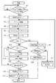
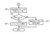
以下、図4及び図5を参照して、本発明による半導体装置の第1の実施の形態における起動処理の動作の詳細を説明する。図4は、本発明による半導体装置の第1の実施の形態におけるブートプログラムの読み出し処理の動作を示すフロー図である。又、図5は、本発明による半導体装置の第1の実施の形態における起動処理の概念図である。本実施の形態では、ブロック201−1〜201−3にブートプログラムが格納されているものとして説明する。(Operation)
The details of the operation of the start-up process in the first embodiment of the semiconductor device according to the present invention will be described below with reference to FIGS. FIG. 4 is a flowchart showing the boot program read processing operation in the first embodiment of the semiconductor device according to the present invention. FIG. 5 is a conceptual diagram of the start-up process in the first embodiment of the semiconductor device according to the present invention. In the present embodiment, description will be made assuming that a boot program is stored in blocks 201-1 to 201-3.
図4を参照して、システムの起動時(例えば、システムの電源オン時や再起動時)にリセット信号が入力されるとCPU4は、内部バスを介してブートプログラムが格納されているフラッシュメモリ200にアクセスする(ステップS1Yes)。CPU4は、バス状態信号READYをネゲートする(ステップS2)。これによって、上位システムからの内部バスに対するアクセスがブロックされる。 Referring to FIG. 4, when a reset signal is input when the system is started (for example, when the system is turned on or restarted), the CPU 4 causes the
次に、CPU4は、アドレス補正回路1Aに対し、ブートプログラムの読み出し先ページのアドレス101を指定する。アドレス指定回路1Aでは、指定されたアドレス101がアドレスレジスタ11に格納される。アドレス指定回路13は、アドレス101の指定に応答してアドレスレジスタ11及びブロックカウンタ12Aを参照して、フラッシュメモリコントローラ2に対しブートプログラムの読出し先のブロック及びアドレスを指定する(ステップS3)。詳細には、当初、CPU4からブロックの先頭ページのアドレス101=0がアドレスレジスタ11に格納される。ブロックカウンタ12Aは初期値としてブロック番号103=1となっている。アドレス指定回路13は、ブロック番号103=1と、アドレス101=0を含むアドレス指定信号109をフラッシュメモリコントローラ2に発行して、データ104の読み出し先のページ202(ブロック201−1のページ202−0)を指定する。 Next, the CPU 4 designates the
フラッシュメモリコントローラ2は、アドレス指定信号109に応答して、アドレス指定信号110及びリードコマンド111をフラッシュメモリ200に発行する。フラッシュメモリ200は、アドレス指定信号110で指定されたアドレス101及びブロック番号103に対応するページ202内のデータ104及び冗長部データ113を、フラッシュメモリコントローラ2を介してECC回路3Aに出力する。詳細には、フラッシュメモリ200は、アドレス指定信号110に基づき、ブロック201−1におけるページ202−0を選択する。又、リードコマンド111に応答してページ202−0内のデータ114−1及び冗長部データ113をフラッシュメモリコントローラ2に出力する。冗長部データ113はECC210−1〜210−4を含む。フラッシュメモリコントローラ2は、出力された冗長部データ113をECCバッファ31に格納し(ステップS4)、データ114−1をデータバッファ32に格納する(ステップS5)。 The
不良判定回路33Aは、ECCバッファ31内の冗長部データ113を読み出す。次に、プログラムデータである128バイトのデータ114−1をデータバッファ32から読み出す。不良判定回路33Aは、データ114−1に対応するECC210−1を用いてデータ114−1に対する不良判定を行う(ステップS6)。ここで実施される不良判定は、データ114−1が訂正不可能なエラー(UCE:Uncorrectable Error)を含むか否かの判定(ステップS7)と、訂正可能なエラー(CE:Correctable Error)を含むか否かの判定(ステップS12)が実行される。 The
ステップS7において、データ114−1がUCEを含まないと判定される場合、ステップ12に移行する(ステップS7 NO)。ステップS12において、CEを含むと判定される場合(ステップS12Yes)、データ114−1に対しエラー訂正が施されてRAM5に格納される(ステップS13、S14)。ステップS12において、訂正可能なエラーを含まないと判定されると、不良判定回路33Aは、データ114−1をRAM5に格納する(ステップS14)。 If it is determined in step S7 that the data 114-1 does not include UCE, the process proceeds to step 12 (NO in step S7). In step S12, when it is determined that CE is included (step S12 Yes), the data 114-1 is subjected to error correction and stored in the RAM 5 (steps S13 and S14). If it is determined in step S12 that no correctable error is included, the
ステップS7において、データ114−1がUCEを含むと判定されると、不良判定回路33Aは不良通知信号105Aをアドレス補正回路1Aに発行し、遷移回数カウンタ22をインクリメントする(ステップS8)。ブロック指定回路21Aは、遷移回数カウンタ22を参照して遷移回数106が最大遷移回数TMと一致しているかを判定する(ステップS9)。ブロック指定回路21Aは遷移回数カウンタ22が示す遷移回数106が最大遷移回数TM(ここではTM=3)と一致する場合(ステップS9Yes)、ERR信号115をCPU4に出力する(ステップS10)。すなわち、全てのブロック201−1〜201−3における同一アドレスのページ202が不良ページである場合、ブロック指定回路21AはERR信号115をCPU4に出力して、ブートプログラムのリード動作を停止させる。 If it is determined in step S7 that the data 114-1 includes UCE, the
遷移回数106が最大遷移回数TMと一致しない場合(ステップS9No)、ブロック指定回路21Aは、ブロックカウンタ12Aを更新し、読み出し先のブロックとして次のブロック201を指定する。ここでは、ブロック指定信号107Aを発行してブロックカウンタ12Aをインクリメントしてブロック番号103を更新する。アドレス指定回路13は、ブロックカウンタ12Aが更新されると、更新されたブロック番号103とアドレスレジスタ11内のアドレス101とに従ってデータの読み出し先のアドレスを補正する(ステップS3)。詳細には、アドレス指定回路13は、更新されたブロック番号103(例えば、ブロック番号=2)と、アドレスレジスタ11内のアドレス101(例えば、アドレス=0)に基づき、読み出し先ページをブロック201−2のページ202−0に指定したアドレス指定信号109を発行する。じ後、ステップS4〜S6に移行する。すなわち、ブロック201−2のページ202−0からデータ114−1及び冗長部データ113を取得して、不良判定回路33Aにてデータ114−1の不良判定が実行される。 When the number of
ステップS14において、データ114−1がRAM5に格納されるとステップ5に移行し、不良判定回路33Aは引き続き、ブロック201−2のページ202−0内からデータ114−2を取得し、対応するECC210−2を参照して不良判定を実行する。この際、エラーがない場合、データ114−2はRAM5に格納される(ステップS5〜S14)。以上のように、ステップS5〜ステップS14を繰り返し、ブロック201−2のページ202−0内の全てのデータ114−1〜114−4がRAM5に格納される。1ページ分のデータ104(データ114−1〜114−4)がRAM5に読み込まれると(ステップS15 Yes)、バス状態信号がアサートされ(ステップS16)、RAM5内のデータ104はCPU4に出力される(ステップS17)。RAM5からデータ104が出力されると遷移回数カウンタ22は初期値にリセットされる。 In step S14, when the data 114-1 is stored in the
以上のように、本発明によるマイクロコンピュータ100Aは、CPU4から指定されたアドレスを保存し、そのアドレスに対応するページからブートプログラムデータを読み出し、ECC制御単位でそのデータの不良判定を行う。この際、不良ページが検出されると、読み出し先のブロックを遷移して、保持しているアドレス101に対応するページ202から再度ブートプログラムデータを読み出す。又、全てのブロックにおいて同一ページが不良ページである場合、ERR信号115が発行され、CPU4の起動処理は停止される。 As described above, the
ここで、ブートプログラムがブロック201の複数ページ(例えばブロック内の全てのページ202−0〜202−31)に格納されている場合、RAM5からデータ104を受け取ったCPU4は、次のページに対応するアドレス101をアドレス補正回路1Aに指定する。アドレスレジスタ11は、指定された新たなアドレス101を保持し、マイクロコンピュータ100Aは上述のステップS3以降の動作に移行する。この際、アドレス指定回路13は、前ページからデータを読み取る際にブロック指定部12によって指定されたブロック番号103と、CPU4によって更新されたアドレス101に基づき、データ104の読み出し先のページ202を指定する。以上のように、マイクロコンピュータ100Aはブロック201−1〜201−3のいずれかにおけるページ202−0〜202−31からブートプログラムをシーケンシャルに読み出し、起動処理を実行することができる。 When the boot program is stored in a plurality of pages of the block 201 (for example, all the pages 202-0 to 202-31 in the block), the CPU 4 that has received the
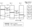
図5は、本発明による半導体装置の第1の実施の形態におけるブートプログラムデータの読み出し処理の概念図である。図5は、左から順にブロック201−1、201−2、201−3、及びホストCPU4から見たフラッシュメモリ(ROM)のイメージ、すなわち、CPU4に読み込まれたブートプログラムデータの読み出し先ブロックとページとの対応関係を示す。以下、図4及び図5を参照して第1の実施の形態におけるブートプログラムデータの読み出し先ページの変更例(ブロックの遷移例)を示す。 FIG. 5 is a conceptual diagram of boot program data read processing in the first embodiment of the semiconductor device according to the present invention. FIG. 5 shows, in order from the left, blocks 201-1, 201-2, 201-3, and the image of the flash memory (ROM) viewed from the host CPU 4, that is, the read destination block and page of the boot program data read by the CPU 4. The correspondence relationship is shown. Hereinafter, a modification example (block transition example) of the boot program data read destination page in the first embodiment will be described with reference to FIGS. 4 and 5.
起動処理が開始されると、ステップS2〜S17を繰り返し、ブロック201−1のページ202−0からプログラムデータがCPU4に読み込まれる。不良判定回路33Aによってブロック201−1のページ202−10が不良ページであると判定されると、ステップS11においてアドレス補正回路1Aは、読み出し先のブロックをブロック201−2に補正する。続いて、ステップS2〜S17を繰り返し、ブロック201−2のページ202−10から順にプログラムデータがCPU4に読み込まれる。ブロック201−2のページ202−15が不良ページと判定されると、アドレス補正回路1Aは読み出し先のブロックをブロック201−3に補正する。続いてステップS2〜S17を繰り返し、ブロック201−3のページ202−15から順にプログラムデータがCPU4に読み込まれる。 When the activation process is started, steps S2 to S17 are repeated, and the program data is read into the CPU 4 from the page 202-0 of the block 201-1. If the
最終ブロックであるブロック201−3のページ202−25が不良ページと判定されると、アドレス補正回路1Aは、最初に読み出し先ブロックとして指定したブロック201−1を次の読み出し先ブロックとして指定する。詳細には、ステップ11において、ブロックカウンタ12Aがブロック番号=3を示しているとき、ブロック指定回路21Aからブロック指定信号107Aが発行されると、ブロックカウンタ12Aは初期値(最初のブロック番号、ここではブロック番号=1)にリセットされる。続くステップS3においてアドレス指定回路13は、アドレスレジスタ11に格納されたアドレス101(例えば、アドレス=25)と、ブロックカウンタ12Aの示すブロック番号103(ここではブロック番号=1)に基づいたアドレス指定信号109を発行する。以下、ステップS4に移行し、CPU4はブロック201−1のページ202−25からページ202−31まで順にプログラムデータを読み出していく。 When it is determined that the page 202-25 of the block 201-3 which is the final block is a defective page, the
以上のように、マイクロコンピュータ100AのCPU4は、ページ202−0〜202−31に格納されたブートプログラムをフラッシュメモリ200から読み出すことができる。この際、CPU4は、不良ページの検出毎に読み出し先のブロックを変更してブートプログラムデータを読み出すことができる。図5を参照して、CPU4から見たブートプログラムデータの読み出し先は、ブロック201−1のページ202−0〜202−9及びページ202−25〜31、ブロック201−2のページ202−10〜202−14、ブロック201−3のページ202−15〜202−24となる。 As described above, the CPU 4 of the
ここで、全てのブロック201−1〜201−3の同一ページ202(例えばページ202−5)が不良ページである場合について説明する。ブロック201−1のページ202−5が不良ページであると判定されると、遷移回数カウンタ22はインクリメントされて遷移回数106=1となる。ブロック指定回路21Aは、遷移回数106が最大遷移回数TM=3と不一致であるためブロック指定回路21Aは、ブロックカウンタ12Aをインクリメントして読み出し先ブロックをブロック201−2に遷移する。続いて、ブロック201−2のページ202−5が不良ページであると判定されると、遷移回数カウンタ22はインクリメントされて遷移回数106=2となる。遷移回数106が最大遷移回数TM=3と不一致であるためブロック指定回路21Aは、ブロックカウンタ12Aをインクリメントして読み出し先ブロックをブロック201−3に遷移する。続いて、ブロック201−3のページ202−5が不良ページであると判定されると、遷移回数カウンタ22はインクリメントされて遷移回数106=3となる。遷移回数106が最大遷移回数TM=3と一致するため、ブロック指定回路21AはERR信号115をCPU4に発行して起動処理を停止する。 Here, the case where the same page 202 (for example, page 202-5) of all the blocks 201-1 to 201-3 is a defective page will be described. When it is determined that the page 202-5 of the block 201-1 is a defective page, the
以上のように、本実施の形態におけるマイクロコンピュータ100Aによれば、同一ブートプログラムが格納された複数のブロック201において、全てのブロックに不良ページが存在していても、不良ページが同一アドレスに存在しない限り、正しくブートプログラムを読み出すことができる。このため、NAND型フラッシュメモリ内に格納されたブートプログラムを利用して安定した起動処理が実現できる。尚、本実施の形態では、NAND型フラッシュメモリからブートプログラムを読み出すことを一例として説明されたが、シーケンシャルに読み出されるデータやプログラムを読み出す半導体装置にも適用できる。 As described above, according to the
又、従来技術による起動処理では、不良ページを検出する毎にブートプログラムの読み出し先のブロックを順に変更しているが、全てのブロックを一巡すると処理を停止してしまう。しかし、本発明によるマイクロコンピュータ100Aによれば、不良ページの検出毎に読み出し先ブロックを変更し、一巡しても最初のブロックからプログラムデータを読み出すことができる。このため、ブートプログラムを格納するために用意するブロック数を少なくでき、メモリ資源を有効に活用することができる。 In the startup process according to the prior art, every time a defective page is detected, the boot program read destination block is changed in order. However, when all the blocks are cycled, the process stops. However, according to the
ここで、NANDフラッシュメモリに格納されたブートプログラムを利用して起動できない確率について、特許文献1に記載の技術と本発明によるマイクロコンピュータ100Aとを比較する。 Here, regarding the probability of not being able to start using the boot program stored in the NAND flash memory, the technique disclosed in
(特許文献1による技術)
起動処理が停止する条件:N個のブロック全てに不良領域が存在する。
起動処理が停止する確率:1/(nCn+nCn−1+nCn−2+・・・+nC2+nC1)
例えば、ブートプログラム格納用のブロックを3個用意した場合、
起動処理が停止する確率は、1/(3C3+3C2+3C1)=1/8=12.5%となる。
(本発明による半導体装置)
起動処理が停止する条件:N個のブロック全てに不良領域が存在し、且つ、その不良領域が同一ページである。
起動処理が停止する確率:1/32N
例えば、ブートプログラム格納用のブロック(1ブロックは32ページ)を3個用意した場合、
起動処理が停止する確率は、32/323=0.98%となる。(Technology according to Patent Document 1)
Condition for stopping the startup process: A defective area exists in all N blocks.
Activation probability processstops: 1 / (n C n + n C n-1 + n C n-2 + ··· +
For example, when three blocks for storing boot programs are prepared,
The probability of starting the process isstopped, the1 / (3 C 3 + 3
(Semiconductor device according to the present invention)
Condition for stopping the activation process: A defective area exists in all N blocks, and the defective area is the same page.
Probability that the startup process will stop: 1/32N
For example, if you prepare 3 blocks for storing boot programs (1 block is 32 pages)
The probability that the activation process is stopped is 32/323 = 0.98%.
以上のように、本発明による半導体装置は、従来技術に比べ、メモリ内の不良領域によって起動処理が停止する確率が格段に減少する。このため、不良率の比較的多いNAND型フラッシュメモリを利用しても安定した起動処理を実現することができる。又、メモリの製造過程において発生した不良のみならず、使用時にブートプログラムの書き換えによって生じた不良に対しても不良回避され得る。更に、不良検出時にブロックの遷移が行われるため、ブートプログラムの書き換えの信頼度が向上され得る。 As described above, in the semiconductor device according to the present invention, the probability that the start-up process is stopped due to the defective area in the memory is remarkably reduced as compared with the related art. For this reason, even if a NAND flash memory having a relatively high defect rate is used, stable start-up processing can be realized. In addition, not only defects that occur in the memory manufacturing process but also defects that are caused by rewriting the boot program during use can be avoided. Furthermore, since the transition of blocks is performed when a defect is detected, the reliability of rewriting the boot program can be improved.
2.第2の実施の形態
第2の実施の形態における本発明による半導体装置は、同一のブートプログラムが格納された複数のブロックを備えるNAND型フラッシュメモリを具備し、読み出しデータのエラー検出に応答して他のブロックの同一ページから当該データの再読み出しを実行する。第2の実施の形態における半導体装置は、主にブートプログラムデータの読み出し先として指定されるメインブロックMBと、メインブロックMBにおいて不良ページが検出されたときのみ、読み出し先として指定されるサブブロックSBとを遷移して不良回避を実行する。以下、図6から図8を参照して第2の実施の形態における半導体装置の詳細を説明する。2. Second Embodiment A semiconductor device according to the second embodiment of the present invention includes a NAND flash memory including a plurality of blocks in which the same boot program is stored, and responds to error detection of read data. The data is read again from the same page in another block. The semiconductor device according to the second embodiment mainly includes a main block MB designated as a boot program data read destination and a sub-block SB designated as a read destination only when a defective page is detected in the main block MB. To avoid failure. Details of the semiconductor device according to the second embodiment will be described below with reference to FIGS.
(構成)
図6は、本発明による半導体装置の第2の実施の形態における構成図である。図6を参照して、本発明による半導体装置は、起動処理を実行するマイクロコンピュータ100Bと、起動処理を実行するためのブートプログラムが格納されるフラッシュメモリ200とを具備する。マイクロコンピュータ100Bは、同一のICチップ上に形成されることが好ましい。又、マイクロコンピュータ100Bとフラッシュメモリ200とが同一ICチップに搭載されていても構わない。第2の実施の形態におけるマイクロコンピュータ100Bは、第1の実施の形態におけるアドレス補正回路1A及びECC回路3Aに替えてアドレス補正回路1B及びECC回路3Bを備える。参照符号が同一の構成は、第1の実施の形態と同様な構成及び動作であるので説明を省略する。又、第2の実施の形態におけるフラッシュメモリ200では、同一のブートプログラムがブロック201−1及び201−2に格納されているものとする。(Constitution)
FIG. 6 is a configuration diagram of a semiconductor device according to a second embodiment of the present invention. Referring to FIG. 6, the semiconductor device according to the present invention includes a
第2の実施の形態におけるアドレス補正回路1Bは、フラッシュメモリコントローラ2に対してデータの読み出し先のページ及びブロックを指定するアドレス指定部10Bと、ECC回路3Bにおける不良判定の結果に基づきデータの読み出し先ブロックを決定するブロック指定部20Bとを具備する。アドレス補正回路1Bは、ECC回路3Bにおけるデータの不良判定の結果に応じて、データの読み出し先ブロックを決定する。通常、アドレス補正回路1BはメインブロックMBをデータ104の読み出し先ブロックに指定するが、不良ページが検出されるとサブブロックSBを読み出し先ブロックとして指定する。又、サブブロックSBから1ページ分のデータ104を読み取ると、再度メインブロックMBを読み出し先ブロックに指定する。 The
アドレス指定部10Bは、アドレスレジスタ11と、ブロックカウンタ12Bと、アドレス指定回路13とを備える。ブロックカウンタ12Bは、ブロック指定部20Bから発行されるブロック指定信号107A及び107Bに応答してブロック番号103を更新する。例えば、ブロックカウンタ12Bは、ブロック指定信号107Bに応答してメインブロックMBのブロック番号にセットされ、ブロック指定信号107Aに応答してサブブロックのブロック番号103にセットされる。詳細には、ブロックカウンタ12Bは、ブロック指定信号107Bに応答して初期値にリセットされ、ブロック指定信号107Aに応答してブロック番号がインクリメントされる。アドレス指定回路13は、データ104の読み出し先のページ202を指定するアドレス101とブロックカウンタ12Bが示すブロック番号103に基づくアドレス指定信号109をフラッシュメモリコントローラ2に発行する。フラッシュメモリコントローラ2は、アドレス指定信号109に対応するブロック201のページ202を読み出し先としてフラッシュメモリ200にアクセスする。 The
ブロック指定部20Bは、ブロック指定回路21Bと遷移回数カウンタ22とを備える。遷移回数カウンタ22は、不良通知信号105Aに応答して遷移回数106をカウントする。ブロック指定回路21Bは、遷移回数カウンタ22の示す遷移回数106、又はECC回路3Bから発行されるデータ出力通知信号105Bに応じて、読み出し先のブロックを決定する。 The
ブロック指定回路21Bは、ECC回路3Bにおいて不良ページが検出されると、ブロック指定信号107Bをブロックカウンタ12Bに発行する。ブロックカウンタ12Bは、ブロック指定信号107Aに応答してブロック番号103がインクリメントされる。又、ブロック201−1〜201−2における同一ページの全てが不良ページと判定された場合、ブロック指定回路21BはERR信号115をCPU4に発行して起動処理を中止する。詳細には、ブロック指定回路21Bは、遷移回数の上限値を示す最大遷移回数TMを保持し、遷移回数106と最大遷移回数TMが一致する場合、ERR信号115をCPU4に発行する。ここでブートプログラム格納用のブロック201はサブブロックSBとメインブロックMBの2つであるので、最大遷移回数TMは2となる。 When a defective page is detected in the
不良ページが検出され、遷移回数106と最大遷移回数TMが一致しない場合、すなわち、メインブロックMBにおいて不良ページが検出された場合、ブロック指定回路21BはサブブロックSBを読み出し先として指定する。この際、ブロック指定回路21Bはブロック指定信号107Aをブロックカウンタ12Bに発行する。ブロックカウンタ12Bは、ブロック指定信号107Aに応答してブロック番号がインクリメントされる。 When a defective page is detected and the
1ページ分のデータ104がRAM5に格納されると、ブロック指定回路21Bは、次の読み出し先ブロックとしてメインブロックMBを指定する。詳細には、ECC回路3Bは、RAM5に1ページ分のデータ114−1〜114−4を出力すると、ブロック指定回路21Bに対しデータ出力通知信号105Bを発行する。ブロック指定回路21Bは、データ出力通知信号105Bに応答してブロック番号103を初期値にリセットするブロック指定信号107Bをブロックカウンタ12Bに発行する。 When the
ECC回路3Bは、ECCバッファ31、データバッファ32、不良判定回路33Bを備える。不良判定回路33Bは、データバッファ32から128バイトのデータ114を抽出して、取得したデータ114に対応するECC210によってデータ114の不良判定を実行する。又、訂正回路を含み、CEを検出するとエラー訂正を実行する。不良判定回路33Bは、データ114がUCEを含むと判定すると遷移回数カウンタ22に不良通知信号105Aを発行する。又、UCEを含まないと判定すると、データ114をRAM5に格納する。ここで、データ114−4をRAM5に格納する際、不良判定回路33Bはブロック指定回路21Bにデータ出力通知信号105Bを発行する。 The
以上のように第2の実施の形態におけるアドレス補正回路1Bは、読み出し先のページから取得したデータが不良である場合、データの読み出し先ページをメインブロックMBからサブブロックSBにおける同一アドレスのページに遷移する。アドレス補正回路1Bは、通常、メインブロックMBであるブロック201−1を読み出し先ブロックとして指定する。この間、不良ページが検出されると、サブブロックSBであるブロック201−2における、不良ページと同一アドレスのページ(ここでは、ページ202−1)に読み出し先を変更する。サブブロックSBからデータ104がCPU4に読み取られると、次の読み出し先としてメインブロックMBが指定され、メインブロックMBの不良ページ以降のページ202(ここでは、ページ202−2)からブートプログラムデータが読み出される。この際、サブブロックSBにおいて不良ページが検出されると、アドレス補正回路1BはERR信号115をCPU4に発行し、起動処理を停止する。 As described above, in the
(動作)
以下、図7及び図8を参照して、本発明による半導体装置の第2の実施の形態における起動処理の動作の詳細を説明する。図7は、本発明による半導体装置の第2の実施の形態における起動処理の動作を示すフロー図である。又、図8は、本発明による半導体装置の第2の実施の形態におけるブートプログラムの読み出し処理の概念図である。本実施の形態では、メインブロックMBとして設定されるブロック201−1とサブブロックSBとして設定される201−2に同一のブートプログラムが格納されているものとして説明する。尚、図面に記載の各ステップに付された参照番号で第1の実施の形態と同一のものは、同一の動作を示すため、その説明を省略する。(Operation)
Hereinafter, with reference to FIG. 7 and FIG. 8, the details of the operation of the start-up process in the second embodiment of the semiconductor device according to the present invention will be described. FIG. 7 is a flowchart showing the operation of the start-up process in the second embodiment of the semiconductor device according to the present invention. FIG. 8 is a conceptual diagram of boot program read processing in the second embodiment of the semiconductor device according to the present invention. In the present embodiment, description will be made on the assumption that the same boot program is stored in the block 201-1 set as the main block MB and 201-2 set as the sub-block SB. Note that the same reference numerals assigned to the respective steps described in the drawings as those in the first embodiment indicate the same operation, and thus the description thereof is omitted.
図7を参照して、システムの起動時(例えば、システムの電源オン時や再起動時)にリセット信号が入力されるとCPU4は、内部バスを介してブートプログラムが格納されているフラッシュメモリ200にアクセスする。以降、第1の実施の形態と同様にステップS1からステップS15までが繰り返され、CPU4によって指定されたアドレス101に対応するページ202からデータ104がRAM5に読み込まれる。ブロック指定回路21Bは、データ104(データ114−1〜114−4)がRAM5に格納されると、次の読み出し先としてブロック201−1(メインブロックMB)を指定する(ステップS18)。詳細には、不良判定回路33Bは、データ114−4をRAM5に格納する際、データ出力通知信号105Bをブロック指定回路21Bに発行する。ブロック指定回路21Bは、データ出力信号105Bに応答してブロック指定信号107Bをブロックカウンタ12Bに発行する。ブロックカウンタ12Bは、ブロック指定信号107Bに応答してメインブロックMBのブロック番号103(ここではブロック201−1のブロック番号103=1)にリセットされる。このため、次にCPU4から読み出し先として指定される次ページからブートプログラムを読み出す際、アドレス補正回路1BはメインブロックMB(ブロック201−1)を読み出し先のブロックとして指定することができる。 Referring to FIG. 7, when a reset signal is input when the system is started (for example, when the system is turned on or restarted), the CPU 4 causes the
1ページ分のデータ104がRAM5に読み込まれると(ステップS15Yes)、バス状態信号がアサートされ(ステップS16)、RAM5内の1ページ分のデータ104はCPU4に出力される(ステップS17)。RAM5から1ページ分のデータ104がCPU4に出力されると遷移回数カウンタ22は初期値にリセットされる。 When the
以上のように、本発明によるマイクロコンピュータ100Bは、CPU4から指定されたアドレス101を保存し、そのアドレス101に対応するページからブートプログラムデータを読み出し、ECC制御単位でそのデータの不良判定を行う。この際、その不良データが検出されると、読み出し先のブロックをメインブロックMBからサブブロックSB遷移して、アドレス101に対応するページ202から再度ブートプログラムデータを読み出す。又、サブブロックSBの同一ページが不良ページである場合は、ERR信号115が発行され、CPU4はブート処理を停止する。更に、サブブロックSBから1ページ分のデータ104を読み出すと、データの読み出し先ブロックをメインブロックMBに変更する。 As described above, the
ここで、ブートプログラムがブロック201の複数ページ(例えばブロック内の全てのページ202−0〜202−31)に格納されている場合、RAM5からデータ104を受け取ったCPU4は、次のページに対応するアドレス101をアドレス補正回路1Bに指定する。アドレスレジスタ11は指定された新たなアドレス101を保持し、マイクロコンピュータ100Bは上述のステップS3以降の動作に移行する。このように、マイクロコンピュータ100Bは、ページ202−0〜202−31のアドレスを順に指定して、ブロック201−1又は201−2のページ202−0〜202−31内のデータ104を読み出し、起動処理を実行する。 When the boot program is stored in a plurality of pages of the block 201 (for example, all the pages 202-0 to 202-31 in the block), the CPU 4 that has received the
図8は、本発明によるマイクロコンピュータ100Bの起動処理におけるブートプログラムデータの読み出し処理の概念図である。図8は、左から順にブロック201−1、201−2及びホストCPU4から見たフラッシュメモリ(ROM)のイメージ、すなわち、CPU4に読み込まれたブートプログラムデータの読み出し先ブロックとページとの対応関係を示す。以下、図7及び図8を参照して第2の実施の形態におけるブートプログラムデータの読み出し先ページの変更例(ブロックの遷移例)を示す。 FIG. 8 is a conceptual diagram of boot program data read processing in the startup processing of the
起動処理が開始されると、ステップS2〜S18を繰り返し、ブロック201−1のページ202−0から順にデータ104がCPU4に読み込まれる。ここで、ブロック201−1のページ202−10とページ202−20が不良ページであるとする。不良判定回路33Bによってブロック201−1のページ202−10が不良ページであると判定されると、アドレス補正回路1Bは、ステップS8〜S11の動作を実行して読み出し先のブロックをブロック201−2に補正する。続いてステップS3に移行してブロック201−2のページ202−10からデータ104がCPU4に読み込まれる。この際、RAM5に202−10内のデータ104が読み込まれると、ブロック指定回路21Bは読み出し先ブロックをブロック201−1に変更する。 When the activation process is started, steps S2 to S18 are repeated, and the
ページ202−10からCPU4にデータ104が読み出されるとステップS2に移行し、CPU4は、次のページ202−11のアドレスをアドレス指定回路1Bに指定する。以降、ステップS2〜S18を繰り返してブロック201−1のページ202−11〜202−19まで読み込まれる。ページ202−20が不良であると判定されると、読み出し先のブロックが変更され、ブロック201−2のブロック201−20からデータ104が読み込まれる。CPU4にデータ104が読み込まれると、読み出し先がブロック201−1に変更される。同様にしてブロック201−1のページ202−21〜202−31まで順にデータ104がCPU4に読み込まれる。 When the
以上のように、マイクロコンピュータ100BのCPU4は、ページ202−0〜202−31に格納されたブートプログラムをフラッシュメモリ200から読み出すことができる。この際、CPU4は、通常、メインブロックMBからブートプログラムデータを読み出すが、不良ページを検出する毎に読み出し先のブロックをサブブロックSBに変更してブートプログラムデータを読み出す。図8を参照して、CPU4から見たブートプログラムデータの読み出し先は、ブロック201−1のページ202−0〜202−9、ページ202−11〜202−19、及びページ202−21〜202−31、ブロック201−2のページ202−10及び202−20となる。 As described above, the CPU 4 of the
本実施の形態におけるマイクロコンピュータ100Bは、同一ブートプログラムが格納されたメインブロックMBとサブブロックSBを備え、メインブロックMBに不良ページが存在すると、サブブロックSBの同一ページからデータを取得して、メインブロックMBの不良ページを回避することができる。すなわち、本発明によるマイクロコンピュータ100Bによれば、メインブロックMBとサブブロックSBの同一アドレスに不良ページが存在しない限り、正しくブートプログラムを読み出すことができる。このため、NAND型フラッシュメモリ内に格納されたブートプログラムを利用して安定した起動処理が実現できる。尚、本実施の形態では、NAND型フラッシュメモリからブートプログラムを読み出すことを一例として説明されたが、シーケンシャルに読み出されるデータやプログラムを読み出す半導体装置にも適用できる。 The
又、従来技術による起動処理では、不良ページを検出する毎にブートプログラムの読み出し先のブロックを順に変更しているが、全てのブロックを一巡すると処理を停止してしまう。しかし、本発明によるマイクロコンピュータ100Bによれば、不良ページの検出毎に読み出し先ブロックをサブブロックに変更し、再びメインブロックからブートプログラムデータを読み出す。このため、ブートプログラムを格納するために用意するブロック数を少なくでき、メモリ資源を有効に活用することができる。 In the startup process according to the prior art, every time a defective page is detected, the boot program read destination block is changed in order. However, when all the blocks are cycled, the process stops. However, according to the
ブロック指定部20Bは、ブロックカウンタ12Bによってブロック番号103をインクリメントし、読み出し先のブロックを決定する。しかし、本実施の形態では、読み出し先として選択されるブロック201の数が2つである。このため、ブロック指定部20Bは、読み出し先のブロックを選択するセレクタを具備する構成としても良い。 The
3.第3の実施の形態
第3の実施の形態における本発明による半導体装置は、同一のブートプログラムが格納された複数のブロックを備えるNAND型フラッシュメモリを具備し、読み出しデータのエラー検出に応答して他のブロックの同一ページから当該データの再読み出しを実行する。第3の実施の形態における半導体装置は、第2の実施の形態と同様に主にブートプログラムデータの読み出し先として指定されるメインブロックMBと、メインブロックMBにおいて不良ページが検出されたときのみ、読み出し先として指定されるサブブロックSBとを遷移して不良回避を実行する。又、第3の実施の形態における半導体装置は、メインブロックMBにおける不良ページの数をカウントする不良カウンタ24と、不良ページの数に応じてサブブロックSBをメインブロックMBに変更するメインブロック指定回路23を備える。更に、第3の実施の形態におけるサブブロックSBは複数設定され、サブブロックSBにおいて不良ページが検出されると、他のサブブロックSBが読み出し先のブロックとして指定され、起動処理が継続される。以下、図9から図12を参照して第3の実施の形態における半導体装置の詳細を説明する。3. Third Embodiment A semiconductor device according to the present invention in a third embodiment includes a NAND flash memory including a plurality of blocks in which the same boot program is stored, and responds to error detection of read data. The data is read again from the same page in another block. As in the second embodiment, the semiconductor device according to the third embodiment mainly includes a main block MB designated as a boot program data read destination and a defective page detected in the main block MB. Defect avoidance is executed by transitioning to the sub-block SB designated as the read destination. The semiconductor device according to the third embodiment includes a
(構成)
図9は、本発明による半導体装置の第3の実施の形態における構成図である。図9を参照して、本発明による半導体装置は、起動処理を実行するマイクロコンピュータ100Cと、起動処理を実行するためのブートプログラムが格納されるフラッシュメモリ200とを具備する。マイクロコンピュータ100Cは、同一のICチップ上に形成されることが好ましい。又、マイクロコンピュータ100Cとフラッシュメモリ200とが同一ICチップに搭載されていても構わない。第3の実施の形態におけるマイクロコンピュータ100Cは、第2の実施の形態におけるアドレス補正回路1B及びECC回路3Bに替えてアドレス補正回路1C及びECC回路3Cを備える。参照符号が同一の構成は、第1及び第2の実施の形態と同様な構成及び動作であるので説明を省略する。又、第3の実施の形態におけるフラッシュメモリ200では、同一のブートプログラムがブロック201−1〜201−3に格納されているものとする。(Constitution)
FIG. 9 is a configuration diagram of a semiconductor device according to a third embodiment of the present invention. Referring to FIG. 9, the semiconductor device according to the present invention includes a microcomputer 100C that executes a startup process, and a
第3の実施の形態におけるアドレス補正回路1Cは、フラッシュメモリコントローラ2に対してデータの読み出し先のページ及びブロックを指定するアドレス指定部10Cと、ECC回路3Cにおける不良判定の結果に基づきデータの読み出し先ブロックを決定するブロック指定部20Cとを具備する。アドレス補正回路1Cは、ECC回路3Cにおけるデータの不良判定の結果に応じて、データの読み出し先ブロックを決定する。通常、アドレス補正回路1CはメインブロックMBをデータの読み出し先ブロックに指定するが、不良ページが検出されるとサブブロックSBを読み出し先ブロックとして指定する。又、サブブロックSBから1ページ分のデータを読み取ると、再度メインブロックMBを読み出し先ブロックに指定する。更に本実施の形態では、複数のサブブロックSB−1、SB−2が設定される。アドレス補正回路1Cは、例えばサブブロックSB−1において不良ページが検出されると、次のサブブロックSB−2を読み出し先のブロックとして指定する。尚、本実施の形態では、同一のブートプログラムが格納されるブロックを3つとしたがこの限りではない。 The
アドレス指定部10Cは、アドレスレジスタ11と、ブロックカウンタ12Cと、アドレス指定回路13とを備える。ブロックカウンタ12Cは、ブロック指定部20Cから発行されるブロック指定信号107A及び107Cに応答してブロック番号103を更新する。例えば、ブロックカウンタ12Cは、ブロック指定信号107Cに応答してメインブロックMBのブロック番号にセットされ、ブロック指定信号107Aに応答してブロック番号がインクリメントされる。アドレス指定回路13は、データの読み出し先のページを指定するアドレス101とブロックカウンタ12Cが示すブロック番号103に基づき、読み出し先のブロック及びページ202を指定するアドレス指定信号109を、フラッシュメモリコントローラ2に発行する。フラッシュメモリコントローラ2は、アドレス指定信号109に対応するブロック201のページ202を読み出し先としてフラッシュメモリ200にアクセスする。 The address specifying unit 10C includes an
ブロック指定部20Cは、ブロック指定回路21Cと遷移回数カウンタ22とメインブロック指定回路23と不良カウンタ24とを備える。遷移回数カウンタ22は、不良通知信号105Aに応答して遷移回数106をカウントする。不良カウンタ24は、ECC回路3Cから発行される不良通知信号105Cに応答して、ブロック201毎の不良ページ数(以下、不良数116と称す)をカウントする。詳細には、不良カウンタ24は、ブロック番号103に対応するカウンタを備え、不良ページが検出される毎に、不良が検出されたブロックに対応するカウンタをインクリメントする。ここで、不良カウンタ24は、ブロックカウンタ12Cが更新されると、最新のブロック番号103を取得し、そのブロック番号103に対応するカウンタを有効にする。不良カウンタ24は、ECC回路3Cから発行される不良通知信号105Cに応答して、有効になっているカウンタをインクリメントする。このように、不良カウンタ24は読み出し先として指定されたブロックの不良ページ数(不良数116)をカウントする。メインブロック指定回路23は、不良カウンタ24が示す不良数116を参照して、メインブロックMBとなるブロック201を決定する。詳細には、メインブロック指定回路23は、不良数116の上限値として設定される最大不良数EMを保持する。又、メインブロック指定回路23は、メインブロックMBのブロック番号(以下、メインブロック番号117と称す)を保持するレジスタを有し、メインブロックMBの不良数116が最大不良数EMと一致する場合、メインブロック番号117を更新する。 The
ブロック指定回路21Cは、遷移回数106、不良数116、メインブロック番号117に応じて次の読み出し先のページを決定する。 The
ブロック指定回路21Cは、ECC回路3Cにおいて不良ページが検出されると、ブロック指定信号107Aをブロックカウンタ12Cに発行する。ブロックカウンタ12Cは、ブロック指定信号107Aに応答してブロック番号103がインクリメントされる。ここで、ブロック201−1〜201−3における同一ページ202の全てが不良ページと判定される場合、ブロック指定回路21CはERR信号115をCPU4に発行して起動処理を中止する。詳細には、ブロック指定回路21Cは、遷移回数の上限値を示す最大遷移回数TMを保持し、遷移回数106と最大遷移回数TMが一致する場合、ERR信号115をCPU4に発行する。ここでブートプログラムの読み出し先として使用するブロックはメインブロックMBと2つのサブブロックSBの合計3つであるので、最大遷移回数TMは3となる。 When a defective page is detected in the
1ページ分のデータ104がRAM5に格納されると、ブロック指定回路21Cは、次の読み出し先ブロックとしてメインブロックMBを指定する。詳細には、ECC回路3Cは、RAM5に1ページ分のデータ114−1〜114−4を出力すると、ブロック指定回路21Cに対しデータ出力通知信号105Bを発行する。ブロック指定回路21Cは、データ出力通知信号105Bに応答して、メインブロックMBを読み出し先に指定するブロック指定信号107Cをブロックカウンタ12Cに発行する。この際、ブロック指定回路21Cは、メインブロック番号117に基づくブロック番号指定信号107Cを発行する。ブロックカウンタ12Cはブロック番号指定信号107Cに応答してメインブロック番号117にセットされる。 When the
ECC回路3Cは、ECCバッファ31、データバッファ32、不良判定回路33Cを備える。不良判定回路33Cは、データバッファ32から128バイトのデータ114を抽出して、取得したデータ114に対応するECC210によってデータ114の不良判定を実行する。又、訂正回路を含み、CEを検出するとエラー訂正を実行する。不良判定回路33Cは、データ114がUCEを含むと判定すると遷移回数カウンタ22に不良通知信号105Aを発行するとともに不良通知信号105Cを不良カウンタ24に発行する。又、不良を含まないと判定すると、データ114をRAM5に格納する。ここで、データ114−4をRAM5に格納する際、不良判定回路33Cはブロック指定回路21Cにデータ出力通知信号105Bを発行する。 The
以上のように第3の実施の形態におけるアドレス補正回路1Cは、読み出し先のページから取得したデータが不良である場合、データの読み出し先ページを他のブロックにおける同一アドレスのページに遷移する。アドレス補正回路1Cは、通常、メインブロックMBを読み出し先ブロックとして指定する。この間、不良ページが検出されると、サブブロックSBにおける不良ページと同一アドレスのページ202に読み出し先を変更する。サブブロックSBからデータ104がCPU4に読み取られると、読み出し先として再度メインブロックMBが指定され、メインブロックMBの不良ページ以降のページ202からブートプログラムが読み出される。又、アドレス補正回路1Cは不良ページ数の多いメインブロックMBに替えて、複数のサブブロックSBのうちの1つを新たなメインブロックMBとして指定する。更に、サブブロックSBにおいて不良ページが検出されると、次のサブブロックSBが読み出し先のブロックとして指定され、データの読み出しが実行される。 As described above, when the data acquired from the read destination page is defective, the
(動作)
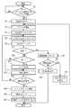
以下、図10から図12を参照して、本発明による半導体装置の第3の実施の形態における起動処理の動作の詳細を説明する。図10は、本発明による半導体装置の第3の実施の形態における起動処理の動作を示すフロー図である。又、図11は、本発明による半導体装置の第3の実施の形態におけるメインブロック指定処理の動作を示すフロー図である。図12は、本発明による半導体装置の第3の実施の形態におけるブートプログラムの読み出し処理の概念図である。本実施の形態では、当初メインブロックMBとして設定されるブロック201−1、サブブロックSB−1として設定される201−2、及びサブブロックSB−2として設定される201−3に同一のブートプログラムが格納されているものとして説明する。尚、図面に記載の各ステップに付された参照番号で第1及び第2の実施の形態と同一のものは、同一の動作を示すため、その説明を省略する。(Operation)
Hereinafter, with reference to FIG. 10 to FIG. 12, details of the operation of the start-up process in the third embodiment of the semiconductor device according to the present invention will be described. FIG. 10 is a flowchart showing the operation of the starting process in the third embodiment of the semiconductor device according to the present invention. FIG. 11 is a flowchart showing the operation of the main block designating process in the third embodiment of the semiconductor device according to the present invention. FIG. 12 is a conceptual diagram of boot program read processing in the third embodiment of the semiconductor device according to the present invention. In the present embodiment, the same boot program is initially set in block 201-1 initially set as main block MB, 201-2 set as subblock SB-1, and 201-3 set as subblock SB-2. Will be described as being stored. In addition, since the same reference numerals given to the respective steps described in the drawings as those in the first and second embodiments indicate the same operation, the description thereof is omitted.
図10を参照して、システムの起動時(例えば、システムの電源オン時や再起動時)にリセット信号が入力されるとCPU4は、内部バスを介してブートプログラムが格納されているフラッシュメモリ200にアクセスする。以降、第1の実施の形態と同様にステップS1からステップS15までが繰り返され、CPU4によって指定されたアドレス101に対応するページ202からデータ104がRAM5に読み込まれる。ブロック指定回路21Cは、データ104(データ114−1〜114−4)がRAM5に格納されると、次の読み出し先としてブロック201−1(メインブロックMB)を指定する(ステップS18)。詳細には、不良判定回路33Cは、データ114−4をRAM5に格納する際、データ出力通知信号105Bをブロック指定回路21Cに発行する。ブロック指定回路21Cは、データ出力信号105Bに応答してブロック指定信号107Cをブロックカウンタ12Cに発行する。ブロックカウンタ12Cは、ブロック指定信号107Cに応答してメインブロックMBのブロック番号(ここではブロック201−1のブロック番号103=1)にセットされる。このため、次のページからブートプログラムを読み出す際、アドレス補正回路1CはメインブロックMB(当初ブロック201−1)を読み出し先のブロックとして指定することができる。 Referring to FIG. 10, when a reset signal is input when the system is started (for example, when the system is turned on or restarted), the CPU 4 causes the
1ページ分のデータ104がRAM5に読み出されると(ステップS15Yes)、バス状態信号がアサートされ(ステップS16)、RAM5内の1ページ分のデータ104はCPU4に出力される(ステップS17)。RAM5から1ページ分のデータ104がCPU4に出力されると遷移回数カウンタ22は初期値にリセットされる。 When the
以上のように、本発明によるマイクロコンピュータ100Cは、CPU4から指定されたアドレス101を保存し、そのアドレスに対応するページからブートプログラムデータを読み出し、ECC制御単位でそのデータの不良判定を行う。この際、その不良データが検出されると、読み出し先のブロックを順に遷移して、アドレス101に対応するページ202から再度ブートプログラムデータを読み出す。例えば、メインブロックMBで不良ページが検出された場合、サブブロックSB−1の同一ページ202がデータの読み出し先として指定される。又、サブブロックSB−1の同一ページで不良ページが検出された場合、更に次のサブブロックSB−2がデータの読み出し先として指定される。更に、第2の実施の形態と同様にサブブロックSBから1ページ分のデータ104を読み出すと、データの読み出し先ブロックはメインブロックMBに変更される。 As described above, the microcomputer 100C according to the present invention stores the
又、第3の実施の形態におけるマイクロコンピュータ100Cでは、メインブロックMBの不良数116が最大不良数EMと一致するとき複数のサブブロックSBのうち1つを選択して新たなメインブロックMBに指定する。以下、図11を参照してメインブロックの指定動作を説明する。 In the microcomputer 100C according to the third embodiment, when the number of
ステップS7において、データ114にUCEが含まれると判定されると、不良カウンタ24は、現在読み出し先として指定されているブロック201に対応するカウンタをインクリメントする(ステップS20)。詳細には、不良ページを検知した不良判定回路33Cは不良通知信号105Cを不良カウンタ24に発行する。不良カウンタ24は、不良通知信号105Cに応答してブロックカウンタ12Cが示すブロック番号103を取得し、そのブロック番号103に対応するカウンタをインクリメントする。 If it is determined in step S7 that the
メインブロック指定回路23は、不良カウンタ24が更新されると、メインブロックMBに対応する不良数116と最大不良数EMとを比較する(ステップS21)。メインブロックMBに対応する不良数116と最大不良数EMが異なる場合、現在のメインブロック番号117を維持する(ステップS22)。メインブロックMBに対応する不良数116と最大不良数EMが同じ場合、メインブロック番号117をインクリメントし、メインブロック番号117を更新する(ステップS23)。例えば、メインブロック番号117はブロック番号=1からブロック番号=2に変更される。すなわち、サブブロックSB−1であるブロック201−2がメインブロックとして指定される。メインブロック指定回路23は、ステップS22又はステップS23で決定したメインブロック番号117を保持する。尚、本実施の形態ではメイン番号117をインクリメントしてメインブロックMBを変更しているが、指定方法はこの限りではない。例えば、不良数116の少ないサブブロックSBをメインブロックとして指定しても構わない。又、ステップS20〜S23のメインブロックMBの指定処理は、ステップS11の読み出し先のブロックの変更処理の前に終了することが好ましい。 When the
ブートプログラムがブロック201の複数ページ(例えばブロック内の全てのページ202−0〜202−31)に格納されている場合、RAM5からデータ104を受け取ったCPU4は、次のページに対応するアドレス101をアドレス補正回路1Cに指定する。アドレスレジスタ11は指定された新たなアドレス101を保持し、マイクロコンピュータ100Cは上述のステップS3以降の動作に移行する。このように、マイクロコンピュータ100Cはページ202−0〜202−31のアドレスを順に指定して、ページ202−0〜202−31内のデータ104を読み出し、起動処理を実行することができる。 When the boot program is stored in a plurality of pages of the block 201 (for example, all the pages 202-0 to 202-31 in the block), the CPU 4 receiving the
図12は、本発明によるマイクロコンピュータ100Cの起動処理におけるブートプログラムデータの読み出し処理の概念図である。図12は、左から順にブロック201−1、202−2、201−3、及びホストCPU4から見たフラッシュメモリ(ROM)のイメージ、すなわち、CPU4に読み出されたブートプログラムデータの読み出し先ブロックとページとの対応関係を示す。以下、図10から図12を参照して第3の実施の形態におけるブートプログラムデータの読み出し先ページの変更例(ブロックの遷移例)を示す。 FIG. 12 is a conceptual diagram of boot program data read processing in the startup processing of the microcomputer 100C according to the present invention. FIG. 12 shows blocks 201-1, 202-2, and 201-3 in order from the left, and an image of a flash memory (ROM) viewed from the host CPU 4, that is, a boot program data read destination block read by the CPU 4. Indicates the correspondence with the page. Hereinafter, a modification example (block transition example) of the boot program data read destination page in the third embodiment will be described with reference to FIGS. 10 to 12.
起動処理が開始されると、ステップS2〜S18を繰り返し、ブロック201−1のページ202−0から順にデータ104がCPU4に読み出される。ここで、ブロック201−1のページ202−2、ページ202−5、及びページ202−10、ブロック201−2のページ202−5及びページ202−15が不良ページであるとする。又、メインブロック指定回路23は、最大不良数EM=3に設定されているものとする。 When the activation process is started, steps S2 to S18 are repeated, and the
データ104の読み出しの際、不良判定回路33Cによってブロック201−1のページ202−2が不良ページであると判定されると、アドレス補正回路1Cは、ステップS8〜S11の動作を実行して読み出し先のブロックをブロック201−2に補正する。又、これと並行して、不良カウンタ24は、ブロック201−1に対応する不良数116をインクリメントする。メインブロック指定回路23は、最大不良数EM=3とブロック201−1に対応する不良数116=1とが異なる値であるので、メインブロック番号117を1に維持する。続いてステップS3に移行してブロック201−2のページ202−2からデータ104がCPU4に読み出される。この際、RAM5に202−2内のデータ104が読み出されると、ブロック指定回路21Cは読み出し先ブロックをブロック201−1に変更する。 When the
ページ202−2からデータ104が読み出されるとステップS2に移行し、CPU4は、次のページ202−3のアドレスをアドレス指定回路1Cに指定する。以降、ステップS2〜S18を繰り返してブロック201−1のページ202−2〜202−4まで読み出される。ページ202−5が不良であると判定されると、上述のようにブロック201−2のブロック201−5からデータの読み出し処理が行われる。又、ブロック201−1の不良数116は2となり、メインブロック番号117は1に維持される。ここで、ブロック201−2のページ202−5も不良ページであると判定されると、アドレス補正回路1Cは、ステップS8〜S11の動作を実行して読み出し先のブロックをブロック201−3に補正する。又、これと並行して、不良カウンタ24は、ブロック201−2に対応する不良数116は1となり、メインブロック番号117は1に維持される。続いてステップS3に移行してブロック201−3のページ202−5からデータ104がCPU4に読み出される。この際、RAM5に202−5内のデータ104が読み出されると、ブロック指定回路21Cは読み出し先ブロックをブロック201−1に変更する。 When the
ページ202−5からデータ104が読み出されるとステップS2に移行し、CPU4は、次のページ202−6のアドレスをアドレス指定回路1Cに指定する。以降、ステップS2〜S18を繰り返してブロック201−1のページ202−6〜202−9まで読み出される。ページ202−10が不良であると判定されると、上述のようにブロック201−2のブロック201−10からデータの読み出し処理が行われる。又、ブロック201−1の不良数116は3となるため、メインブロック指定回路23は、メインブロック番号117を2に変更する。すなわち、ページ202−11以降のデータの読み出し処理は、ブロック201−2がメインブロックMBとして使用される。ページ202−10からRAM5にデータ104が読み出されると、ブロック指定回路21Cは読み出し先ブロックを新たなメインブロックMBであるブロック201−2に変更する。 When the
ページ202−10からデータ104が読み出されるとステップS2に移行し、CPU4は、次のページ202−11のアドレスをアドレス指定回路1Cに指定する。以降、ステップS2〜S18を繰り返してブロック201−2のページ202−11〜202−14まで読み出される。ページ202−15が不良であると判定されると、上述のようにブロック201−3のブロック201−15からデータの読み出し処理が行われる。又、ブロック201−2の不良数116は2となり、メインブロック番号117は2に維持される。以降、同様にステップS2〜ステップS18を繰り返し、ブロック201−2のページ202−16〜202−31からデータ104がCPU4に読み出される。 When the
以上のように、マイクロコンピュータ100CのCPU4は、ページ202−0〜202−31に格納されたブートプログラムをフラッシュメモリ200から読み出すことができる。この際、CPU4は、通常、メインブロックMBからブートプログラムデータを読み出すが、不良ページを検出する毎に読み出し先のブロックをサブブロックSBに変更してブートプログラムデータを読み出す。図12を参照して、CPU4から見たブートプログラムデータの読み出し先は、ブロック201−1のページ202−0〜202−1、ページ202−3〜202−4、及びページ202−6〜202−9、ブロック201−2のページ202−2、ページ202−10〜202−14、ページ202−16〜202−31、ブロック201−3のページ202−5、ページ202−15となる。 As described above, the CPU 4 of the
本実施の形態におけるマイクロコンピュータ100Cは、同一ブートプログラムが格納されたメインブロックMBとサブブロックSBを備え、メインブロックMBに不良ページが存在すると、サブブロックSBの同一ページからデータを取得して、メインブロックMBの不良ページを回避することができる。又、本実施の形態ではサブブロックSBを複数備えるため、サブブロックSBから取得したデータに不良が含まれていても更に次のサブブロックSBの同一ページからデータを取得することができる。すなわち、本発明によるマイクロコンピュータ100Cによれば、第1の実施の形態と同様に、ブートプログラムが格納された全てのブロックの同一アドレスに不良ページが存在しない限り、正しくブートプログラムを読み出すことができる。又、不良数116の多いメインブロックMBの使用を停止し、サブブロックSB−1をメインブロックMBに変更することで、より信頼性の高い起動処理が実現できる。このため、NAND型フラッシュメモリ内に格納されたブートプログラムを利用して安定した起動処理が実現できる。尚、本実施の形態では、NAND型フラッシュメモリからブートプログラムを読み出すことを一例として説明されたが、シーケンシャルに読み出されるデータやプログラムを読み出す半導体装置にも適用できる。 The microcomputer 100C according to the present embodiment includes a main block MB and a sub block SB in which the same boot program is stored. When a defective page exists in the main block MB, data is acquired from the same page in the sub block SB. Bad pages in the main block MB can be avoided. In addition, since the present embodiment includes a plurality of sub-blocks SB, data can be acquired from the same page of the next sub-block SB even if the data acquired from the sub-block SB includes a defect. That is, according to the microcomputer 100C of the present invention, as in the first embodiment, the boot program can be read correctly as long as there is no defective page at the same address in all the blocks in which the boot program is stored. . Further, by stopping the use of the main block MB having a large number of
又、従来技術による起動処理では、不良ページを検出する毎にブートプログラムの読み出し先のブロックを順に変更しているが、全てのブロックを一巡すると処理を停止してしまう。しかし、本発明によるマイクロコンピュータ100Cによれば、不良ページの検出毎に読み出し先ブロックをサブブロックに変更し、再びメインブロックからブートプログラムデータを読み出す。このため、ブートプログラムを格納するために用意するブロック数を少なくでき、メモリ資源を有効に活用することができる。 In the startup process according to the prior art, every time a defective page is detected, the boot program read destination block is changed in order. However, when all the blocks are cycled, the process stops. However, according to the microcomputer 100C of the present invention, every time a defective page is detected, the read destination block is changed to a sub block, and the boot program data is read from the main block again. For this reason, the number of blocks prepared for storing the boot program can be reduced, and memory resources can be used effectively.
本実施の形態では、信頼性の高いブロック201をメインブロックMBとして選択して使用できるため、第2の実施の形態に比べ、更に安定してブート処理を実行することができる。 In the present embodiment, since the highly reliable block 201 can be selected and used as the main block MB, the boot process can be executed more stably than in the second embodiment.
以上、本発明の実施の形態を詳述してきたが、具体的な構成は上記実施の形態に限られるものではなく、本発明の要旨を逸脱しない範囲の変更があっても本発明に含まれる。例えば、第3の実施の形態において、3つのブロック201のうち、2つのブロックをブートプログラムの読み出し先のブロックとして設定し、1つを予備として使用しても良い。この場合、最大遷移回数TMは2に設定される。詳細には、当初、ブロック201−1がメインブロックMB、ブロック201−2がサブブロックSBとして使用され、ブロック201−1又はブロック201−2からブートプログラムが読み出される。この際、ブロック201−3は予備として設定され、読み取り先として指定されない。そして、ブロック201−1の不良ページ数(不良数116)が最大不良回数EMを越えると、メインブロックMBは201−2に変更され、当初予備としていたブロック201−3がサブブロックSBとして使用される。以降、第2の実施の形態と同様に2つのブロック201−2及び201−3からブートプログラムがCPU4に読み出される。 The embodiment of the present invention has been described in detail above, but the specific configuration is not limited to the above-described embodiment, and changes within a scope not departing from the gist of the present invention are included in the present invention. . For example, in the third embodiment, of the three blocks 201, two blocks may be set as the boot program read destination blocks, and one may be used as a spare. In this case, the maximum number of transitions TM is set to 2. Specifically, initially, the block 201-1 is used as the main block MB and the block 201-2 is used as the sub-block SB, and the boot program is read from the block 201-1 or the block 201-2. At this time, the block 201-3 is set as a spare and is not designated as a reading destination. When the number of defective pages (number of defects 116) of the block 201-1 exceeds the maximum number of defects EM, the main block MB is changed to 201-2, and the initially reserved block 201-3 is used as the sub-block SB. The Thereafter, the boot program is read out from the two blocks 201-2 and 201-3 to the CPU 4 as in the second embodiment.
又、本実施の形態では、ブートプログラムをメモリから読み出して実行するマイクロコンピュータを一例に説明されたが、これに限らず、メモリからシーケンシャルにデータを読み出す半導体装置に適用できる。 In this embodiment, the microcomputer that reads and executes the boot program from the memory has been described as an example. However, the present invention is not limited to this, and the present invention can be applied to a semiconductor device that reads data sequentially from the memory.
1A、1B、1C:アドレス補正回路
10A、10B、10C:アドレス指定部
11:アドレスレジスタ
12A、12B、12C:ブロックカウンタ
13:アドレス指定回路
20A、20B、20C:ブロック指定部
21A、21B、21C:ブロック指定回路
22:遷移回数カウンタ
23:メインブロック指定回路
24:不良カウンタ
2:フラッシュメモリコントローラ
3A、3B、3C:ECC回路
31:ECCバッファ
32:データバッファ
33A、33B、33C:不良判定回路
4:CPU
5:RAM
100A、100B、100C:マイクロコンピュータ
200:フラッシュメモリ
101:アドレス
103:ブロック番号
104、114、114−1〜114−4:データ
105A、105C:不良通知信号
105B:データ出力通知信号
106:遷移回数
107A、107B、107C:ブロック指定信号
109、110:アドレス指定信号
111:リードコマンド
113:冗長部データ
115:ERR信号
116:不良回数
117:メイン番号
201、201−1〜201−n:ブロック
202、202−0〜202−31:ページ
210、210−1〜210−4:ECC
MB:メインブロック
SB:サブブロック
TM:最大遷移回数
EM:最大エラー回数1A, 1B, 1C:
5: RAM
100A, 100B, 100C: Microcomputer 200: Flash memory 101: Address 103:
MB: Main block SB: Sub block TM: Maximum number of transitions EM: Maximum number of errors
Claims (17)
Translated fromJapanese前記複数の格納領域の各々には、前記ブートプログラムが複数のプログラムデータとして格納され、
前記格納領域から前記複数のプログラムデータの各々を読み出すメモリコントローラと、
前記読み出されたプログラムデータの不良判定を行う不良判定回路と、
前記複数の格納領域は、メインブロックとして設定される格納領域と、サブブロックとして設定される格納領域を含み、
前記メモリコントローラは、CPUから指定されたプログラムデータをメインブロックとして設定される格納領域から読み出し、前記読み出されたプログラムデータが前記不良判定回路において不良と判定される場合、サブブロックとして設定される格納領域から、前記不良と判定されたプログラムデータに対応する前記プログラムデータを読み出し、前記メインブロックに設定される格納領域において不良と判定されたプログラムデータの数が閾値を超える場合、サブブロックとして設定された格納領域をメインブロックとして、前記CPUから新たに指定されたプログラムデータの読み出しを行う
半導体装置。A semiconductor device having a plurality of storage areas each storing the same boot program and performing access control to a memory,
In each of the plurality of storage areas, the boot program is stored as a plurality of program data,
A memory controller for reading each of the plurality of program data from the storage area;
A failure determination circuit for determining failure of the read program data;
The plurality of storage areas include a storage area set as a main block and a storage area set as a sub-block,
The memory controller, ifyou read outfrom the storage area set program data designated by the CPU as the mainblock,the read out program data is determined to be defective in the defect determination circuit,configured as a sub-blockIf the storagearea isto read out the program data corresponding to the program data is determined as thedefective, the number of program data is determined to be defective in the storage area that is set in the main block exceeds a threshold value, A semiconductor devicethat reads newly specified program data from the CPU using a storage area set as a sub-block as a main block .
前記指定されたプログラムデータには、アドレスが対応付けられており、
CPUから指定される前記アドレスを読み出し先のアドレスとして前記メモリコントローラに指定するとともに、読み出し先の格納領域を前記メモリコントローラに指定するアドレス補正回路を更に具備し、
前記メモリコントローラは、前記読み出し先のアドレスに対応するプログラムデータを前記読み出し先の格納領域から読み出し、
前記アドレス補正回路は、前記CPUから指定される前記アドレスを保持し、前記読み出されたプログラムデータが不良判定回路において不良と判定される場合、前記不良と判定されたプログラムデータが格納された格納領域とは異なる格納領域を、前記読み出し先の格納領域として指定し、前記保持するアドレスを前記読み出し先のアドレスとして指定する
半導体装置。The semiconductor device according to claim1 ,
An address is associated with the designated program data,
The address specified by the CPU is designated as the read destination address to the memory controller, and further includes an address correction circuit for designating the read destination storage area to the memory controller,
The memory controller reads program data corresponding to the read destination address from the read destination storage area,
The address correction circuit holds the address designated by the CPU, and stores the program data determined to be defective when the read program data is determined to be defective in the defect determination circuit. A semiconductor device that designates a storage area different from the area as the storage area of the read destination and designates the held address as the address of the read destination.
前記複数の格納領域の各々は、前記ブートプログラムの複数のプログラムデータをそれぞれ格納する複数の単位格納領域を備え、
前記複数の単位格納領域の各々から、前記複数のプログラムデータの各々を読み出すメモリコントローラと、
前記読み出されたプログラムデータの不良判定を行う不良判定回路とを具備し、
前記複数の格納領域は、メインブロックとして設定される格納領域と、サブブロックとして設定される格納領域を含み、
前記メモリコントローラは、CPUから指定されたプログラムデータをメインブロックとして設定される格納領域から読み出し、前記読み出されたプログラムデータが前記不良判定回路において不良と判定される場合、サブブロックとして設定される格納領域の、前記不良と判定されたプログラムデータが格納された単位格納領域に対応する単位格納領域から前記プログラムデータを読み出し、前記メインブロックとして設定される格納領域において不良と判定されたプログラムデータの数が閾値を超える場合、サブブロックとして設定された格納領域をメインブロックとして、前記CPUから新たに指定されたプログラムデータの読み出しを行う
半導体装置。A semiconductor device for controlling access to a memory having a plurality of storage areas each storing the same boot program,
Each of the plurality of storage areas includes a plurality of unit storage areas for storing a plurality of program data of the boot program,
A memory controller for reading each of the plurality of program data from each of the plurality of unit storage areas;
A failure determination circuit for performing a failure determination of the read program data,
The plurality of storage areas include a storage area set as a main block and a storage area set as a sub-block,
The memory controller, ifyou read outfrom the storage area set program data designated by the CPU as the mainblock,the read out program data is determined to be defective in the defect determination circuit,configured as a sub-block the storagearea is,the above-out determined to be defective unit storage areas in which the program data corresponding to the unit storage areas stored are read the programdata, is determined to be defective in the storage area set as the main block A semiconductor devicethat reads out newly designated program data from the CPU using a storage area set as a sub-block as a main block when the number of program data exceeds a threshold .
前記複数の単位格納領域のそれぞれにはアドレスが対応付けられ、同一アドレスに対応する単位格納領域には同一の前記プログラムデータが格納され、
前記CPUから指定される前記アドレスを読み出し先のアドレスとして前記メモリコントローラに指定するとともに、読み出し先の格納領域を前記メモリコントローラに指定するアドレス補正回路を更に具備し、
前記メモリコントローラは、前記読み出し先の格納領域における前記読み出し先のアドレスに対応する単位格納領域から前記プログラムデータを読み出し、
前記アドレス補正回路は、前記CPUから指定される前記アドレスを保持し、前記読み出されたプログラムデータが不良判定回路において不良と判定される場合、前記不良と判定されたプログラムデータが格納された格納領域とは異なる格納領域を、前記読み出し先の格納領域として指定し、前記保持するアドレスを前記読み出し先のアドレスとして指定する
半導体装置。The semiconductor device according to claim3 .
An address is associated with each of the plurality of unit storage areas, and the same program data is stored in the unit storage areas corresponding to the same address,
The address designated by the CPU is designated as the read destination address to the memory controller, and further includes an address correction circuit for designating the read destination storage area to the memory controller,
The memory controller reads the program data from a unit storage area corresponding to the read destination address in the read destination storage area;
The address correction circuit holds the address designated by the CPU, and stores the program data determined to be defective when the read program data is determined to be defective in the defect determination circuit. A semiconductor device that designates a storage area different from the area as the storage area of the read destination and designates the held address as the address of the read destination.
前記アドレス補正回路は、前記読み出し先の格納領域に対応付けられた領域番号を保持し、前記CPUからの新たなアドレスの指定に応答して、前記領域番号に対応する格納領域を次の読み出し先の格納領域として指定し、前記新たなアドレスを次の読み出し先のアドレスとして指定する
半導体装置。The semiconductor device according to claim2 or 4 ,
Said address correction circuit holds a region number associated with a storage area of the read destination, in response tosaid specified new address from the CPU, the corresponding storage areas of the next reading destination into the area number A semiconductor device that designates the new address as a next read destination address.
前記複数の格納領域は第1の格納領域を含み、
前記アドレス補正回路は、前記第1の格納領域に対応付けられた領域番号をメインブロックとして指定するメイン番号として保持し、前記CPUからの新たなアドレスの指定に応答して、前記メイン番号に対応する第1の格納領域を次の読み出し先の格納領域として指定し、前記新たなアドレスを前記読み出し対象のアドレスとして指定する
半導体装置。The semiconductor device according to claim5 ,
Theplurality of storage areas include a first storage area;
The address correction circuit holds an area number associated with the first storage areaas a main number that isdesignated as a main block, and responds to the designation of a new address from the CPU and corresponds to the main number. A first storage area to be designated as a storage area to be read next, and the new address to be designated as an address to be read.
前記複数の格納領域は、第2の格納領域を含み、
前記アドレス補正回路は、前記第1の格納領域から読み出され、前記不良判定回路において不良であると判定されたプログラムデータの数が閾値を超える場合、前記第2の格納領域に対応付けられた領域番号を新たなメイン番号として保持する
半導体装置。The semiconductor device according to claim6 .
The plurality of storage areas include a second storage area;
The address correction circuit is associated with the second storage area when the number of program data read from the first storage area and determined to be defective by the defect determination circuit exceeds a threshold value. A semiconductor device that holds an area number as a new main number.
前記メモリは、NAND型フラッシュメモリであり、
前記複数の格納領域のそれぞれは、前記複数の単位格納領域である複数のページを備えるブロックである
半導体装置。The semiconductor device according to claim3 .
The memory is a NAND flash memory,
Each of the plurality of storage areas is a block including a plurality of pages that are the plurality of unit storage areas.
前記不良判定回路は、前記ページ内に格納されるECC(Error Correction Code)を用いて前記プログラムデータの不良判定を行う
半導体装置。The semiconductor device according to claim8 ,
The defect determination circuit performs a defect determination on the program data by using ECC (Error Correction Code) stored in the page.
半導体装置。The semiconductor device according to claims 19, the semiconductor device further comprising said memory.
前記不良判定回路において、メインブロックとして設定される格納領域から読み出されたプログラムデータの不良が検出されると、当該格納領域の不良回数をカウントする不良カウンタと、 In the defect determination circuit, when a defect in the program data read from the storage area set as the main block is detected, a defect counter that counts the number of defects in the storage area;
メインブロックを指定するメイン番号と前記閾値を保持するブロック指定回路と A main number for designating a main block and a block designating circuit for holding the threshold value;
を更に具備し、 Further comprising
前記ブロック指定回路は、前記不良回数が前記閾値を超える場合、前記メイン番号を他の格納領域に対応付けられた領域番号に変更する The block designating circuit changes the main number to an area number associated with another storage area when the number of failures exceeds the threshold value.
半導体装置。 Semiconductor device.
前記複数の格納領域の各々には、前記ブートプログラムが複数のプログラムデータとして格納され、
前記複数の格納領域は、メインブロックとして設定される格納領域と、サブブロックとして設定される格納領域を含み、
(A)メモリコントローラが、CPUから指定されたプログラムデータをメインブロックとして設定される格納領域から読み出すステップと、
(B)不良判定回路が、前記読み出されたプログラムデータの不良判定を行うステップと、
(C)前記ステップ(B)において不良と判定される場合、前記メモリコントローラが、サブブロックとして設定される格納領域から、前記不良と判定されたプログラムデータに対応する前記プログラムデータを読み出すステップと、
(D)前記メインブロックとして設定される格納領域において不良と判定されたプログラムデータの数が閾値を超える場合、前記メモリコントローラが、サブブロックとして設定された格納領域をメインブロックとして、前記CPUから新たに指定されたプログラムデータの読み出しを行うステップと
を具備する
起動方法。A boot method for accessing a memory having a plurality of storage areas each storing the same boot program and reading the boot program,
In each of the plurality of storage areas, the boot program is stored as a plurality of program data,
The plurality of storage areas include a storage area set as a main block and a storage area set as a sub-block,
(A) a step in which the memory controller readsprogram data designated by theCPU from a storage area set as a main block ;
(B) a defect determination circuit performing a defect determination on the read program data;
(C) when it is determined as defective in the step (B), the memory controller reads the program data corresponding to the program data determined as defective froma storage areaset as a sub-block;
(D) When the number of program data determined to be defective in the storage area set as the main block exceeds a threshold, the memory controller newly sets the storage area set as a sub-block as the main block from the CPU. Reading the program data specified in
An activation method comprising:
前記指定されたプログラムデータには、アドレスが対応付けられており、
前記ステップ(A)は、
アドレス補正回路が、前記CPUから指定される前記アドレスを読み出し先のアドレスとして前記メモリコントローラに指定するとともに、読み出し先の格納領域を前記メモリコントローラに指定するステップと、
前記メモリコントローラが、前記読み出し先のアドレスに対応するプログラムデータを前記読み出し先の格納領域から読み出すステップとを備え、
前記ステップ(C)は、
前記アドレス補正回路が、前記CPUから指定される前記アドレスを保持するステップと、
前記ステップ(B)において不良と判定される場合、前記メモリコントローラが、前記不良と判定されたプログラムデータが格納された格納領域とは異なる格納領域を、前記読み出し先の格納領域として指定し、前記保持するアドレスを前記読み出し先のアドレスとして指定するステップとを備える
起動方法。The activation method according to claim12 , wherein
An address is associated with the designated program data,
The step (A ) includes:
An address correction circuit designating the address designated by the CPU as a read destination address to the memory controller, and designating a read destination storage area to the memory controller;
The memory controller comprising: reading program data corresponding to the read destination address from the read destination storage area;
The step (C ) includes:
The address correction circuit holding the address designated by the CPU;
When it is determined that the memory is defective in the step (B), the memory controller designates a storage area different from the storage area where the program data determined to be defective is stored as the storage area of the read destination, And a step of designating an address to be held as an address of the reading destination.
前記ステップ(A)は、
前記アドレス補正回路が、前記読み出し先の格納領域に対応付けられた領域番号を保持するステップと、
前記アドレス補正回路が、前記CPUからの新たなアドレスの指定に応答して、前記領域番号に対応する格納領域を次の読み出し先の格納領域として指定し、前記新たなアドレスを次の読み出し先のアドレスとして指定するステップとを更に備える
起動方法。The activation method according to claim13 ,
The step (A ) includes:
The address correction circuit holding an area number associated with the storage area of the read destination;
Said address correction circuit is responsive to specify a new address fromsaid CPU, said storage area corresponding to the area number specified as a storage area for the next reading destination, the new address of the next reading destination And a step of designating as an address.
前記複数の格納領域は第1の格納領域を含み、
前記アドレス補正回路が、前記第1の格納領域に対応付けられた領域番号をメイン番号として保持するステップと、
前記CPUからの新たなアドレスの指定に応答して、前記メイン番号に対応する第1の格納領域を次の読み出し先の格納領域として指定し、前記新たなアドレスを前記読み出し対象のアドレスとして指定するステップとを更に具備する
起動方法。The activation method according to claim14 ,
Theplurality of storage areas include a first storage area;
The address correction circuit holding the area number associated with the first storage area as a main number;
In response to the designation of a new address from the CPU, the first storage area corresponding to the main number is designated as the storage area of the next read destination, and the new address is designated as the read target address. And a starting method.
前記複数の格納領域は、第2の格納領域を含み、
前記第1の格納領域から読み出され、前記不良判定回路において不良であると判定されたプログラムデータの数が閾値を超える場合、前記アドレス補正回路が前記第2の格納領域に対応付けられた領域番号を新たなメイン番号として保持するステップを更に備える
起動方法。The activation method according to claim15 , wherein
The plurality of storage areas include a second storage area;
An area in which the address correction circuit is associated with the second storage area when the number of program data read from the first storage area and determined to be defective in the defect determination circuit exceeds a threshold value An activation method further comprising the step of holding the number as a new main number.
前記ステップ(D)は、 The step (D)
メインブロックとして設定される格納領域から読み出されたプログラムデータの不良が検出されると、カウンタが、当該格納領域の不良回数をカウントするステップと、 When a defect in the program data read from the storage area set as the main block is detected, the counter counts the number of defects in the storage area;
メインブロックを指定するメイン番号と前記閾値を保持するブロック指定回路が、前記不良回数が前記閾値を超える場合、前記メイン番号を他の格納領域に対応付けられた領域番号に変更するステップと A block specifying circuit for holding a main number for specifying a main block and the threshold value, and if the number of defects exceeds the threshold value, changing the main number to an area number associated with another storage area;
を備える With
起動方法。 starting method.
Priority Applications (2)
| Application Number | Priority Date | Filing Date | Title |
|---|---|---|---|
| JP2006131505AJP4840859B2 (en) | 2006-05-10 | 2006-05-10 | Semiconductor device and startup method |
| US11/798,092US8037358B2 (en) | 2006-05-10 | 2007-05-10 | Semiconductor device and boot method for the same |
Applications Claiming Priority (1)
| Application Number | Priority Date | Filing Date | Title |
|---|---|---|---|
| JP2006131505AJP4840859B2 (en) | 2006-05-10 | 2006-05-10 | Semiconductor device and startup method |
Publications (2)
| Publication Number | Publication Date |
|---|---|
| JP2007304781A JP2007304781A (en) | 2007-11-22 |
| JP4840859B2true JP4840859B2 (en) | 2011-12-21 |
Family
ID=38838663
Family Applications (1)
| Application Number | Title | Priority Date | Filing Date |
|---|---|---|---|
| JP2006131505AExpired - Fee RelatedJP4840859B2 (en) | 2006-05-10 | 2006-05-10 | Semiconductor device and startup method |
Country Status (2)
| Country | Link |
|---|---|
| US (1) | US8037358B2 (en) |
| JP (1) | JP4840859B2 (en) |
Families Citing this family (20)
| Publication number | Priority date | Publication date | Assignee | Title |
|---|---|---|---|---|
| US7543056B2 (en)* | 2002-01-15 | 2009-06-02 | Mcafee, Inc. | System and method for network vulnerability detection and reporting |
| JP4840859B2 (en)* | 2006-05-10 | 2011-12-21 | ルネサスエレクトロニクス株式会社 | Semiconductor device and startup method |
| US7765426B2 (en)* | 2007-06-07 | 2010-07-27 | Micron Technology, Inc. | Emerging bad block detection |
| US7926072B2 (en) | 2007-10-01 | 2011-04-12 | Spring Design Co. Ltd. | Application programming interface for providing native and non-native display utility |
| US8276043B2 (en)* | 2008-03-01 | 2012-09-25 | Kabushiki Kaisha Toshiba | Memory system |
| KR20100098969A (en)* | 2009-03-02 | 2010-09-10 | 삼성전자주식회사 | Semiconductor device for improving reliability of error correction codes, semiconductor system having the same, and method for processing error correction code |
| JPWO2011001486A1 (en)* | 2009-06-30 | 2012-12-10 | パナソニック株式会社 | Data processing method, semiconductor integrated circuit |
| US8726130B2 (en)* | 2010-06-01 | 2014-05-13 | Greenliant Llc | Dynamic buffer management in a NAND memory controller to minimize age related performance degradation due to error correction |
| US8589730B2 (en)* | 2010-08-31 | 2013-11-19 | Apple Inc. | Handling errors during device bootup from a non-volatile memory |
| JP5330428B2 (en) | 2011-02-21 | 2013-10-30 | 株式会社東芝 | Data storage device and error detection and correction method |
| US8726087B2 (en) | 2011-03-18 | 2014-05-13 | Denso International America, Inc. | System and method for curing a read inability state in a memory device |
| WO2012140710A1 (en)* | 2011-04-14 | 2012-10-18 | パナソニック株式会社 | Boot control device, boot system, and boot control method |
| US9424134B2 (en)* | 2014-03-28 | 2016-08-23 | Intel Corporation | Boot management in a non-volatile memory system |
| JP2015230611A (en)* | 2014-06-05 | 2015-12-21 | 富士通株式会社 | Electronic device and method for controlling electronic device |
| US9703631B2 (en) | 2015-03-20 | 2017-07-11 | Burlywood, LLC | Storage emulation in a storage controller |
| US9997251B2 (en)* | 2015-03-26 | 2018-06-12 | Burlywood, LLC | Medium defect management method for storage systems requiring an integrated controller |
| JP2017045405A (en)* | 2015-08-28 | 2017-03-02 | 株式会社東芝 | Memory system |
| KR102256472B1 (en)* | 2015-09-24 | 2021-05-26 | 한화테크윈 주식회사 | Method for executing and updating boot program |
| TWI573033B (en)* | 2016-01-14 | 2017-03-01 | 群聯電子股份有限公司 | Data searching method, memory storage device and memory control circuit unit |
| JP2020087293A (en) | 2018-11-30 | 2020-06-04 | キヤノン株式会社 | Information processing apparatus and method of controlling information processing apparatus |
Family Cites Families (17)
| Publication number | Priority date | Publication date | Assignee | Title |
|---|---|---|---|---|
| US5960445A (en)* | 1996-04-24 | 1999-09-28 | Sony Corporation | Information processor, method of updating a program and information processing system |
| JP2000148467A (en)* | 1998-11-05 | 2000-05-30 | Sharp Corp | Information processing apparatus, basic system program rewriting method for information processing apparatus, and recording medium storing basic system program rewriting program for information processing apparatus |
| JP4165990B2 (en)* | 1999-12-20 | 2008-10-15 | Tdk株式会社 | MEMORY CONTROLLER, FLASH MEMORY SYSTEM PROVIDED WITH MEMORY CONTROLLER, AND METHOD FOR WRITEING DATA TO FLASH MEMORY |
| US20080256352A1 (en)* | 2000-01-06 | 2008-10-16 | Super Talent Electronics, Inc. | Methods and systems of booting of an intelligent non-volatile memory microcontroller from various sources |
| JP2003242044A (en)* | 2002-02-18 | 2003-08-29 | Hitachi Kokusai Electric Inc | Microcomputer circuit |
| JP2004013477A (en)* | 2002-06-06 | 2004-01-15 | Nec Viewtechnology Ltd | Method for selecting and updating boot program and flash memory using the same |
| KR100532413B1 (en)* | 2002-12-02 | 2005-12-02 | 삼성전자주식회사 | apparatus and method for protecting flash memory |
| JP2004355560A (en)* | 2003-05-30 | 2004-12-16 | Sony Corp | Starting device |
| US7594135B2 (en)* | 2003-12-31 | 2009-09-22 | Sandisk Corporation | Flash memory system startup operation |
| JP4534498B2 (en)* | 2004-01-28 | 2010-09-01 | ソニー株式会社 | Semiconductor device and its startup processing method |
| JP2005242903A (en)* | 2004-02-27 | 2005-09-08 | Sony Corp | Memory device, and memory control method and device |
| JP4245585B2 (en)* | 2005-06-13 | 2009-03-25 | Tdk株式会社 | Memory controller, flash memory system, and flash memory control method |
| US20070079024A1 (en)* | 2005-09-30 | 2007-04-05 | Freescale Semiconductor, Inc. | Circuit and method for detecting non-volatile memory during a boot sequence |
| JP4840859B2 (en)* | 2006-05-10 | 2011-12-21 | ルネサスエレクトロニクス株式会社 | Semiconductor device and startup method |
| JP4153535B2 (en)* | 2006-05-30 | 2008-09-24 | Tdk株式会社 | MEMORY CONTROLLER, FLASH MEMORY SYSTEM PROVIDED WITH MEMORY CONTROLLER, AND FLASH MEMORY CONTROL METHOD |
| US8341491B2 (en)* | 2007-07-16 | 2012-12-25 | Cadence Design Systems, Inc. | System and method for providing data integrity in a non-volatile memory system |
| JP2009157632A (en)* | 2007-12-26 | 2009-07-16 | Toshiba Corp | Information processing device |
- 2006
- 2006-05-10JPJP2006131505Apatent/JP4840859B2/ennot_activeExpired - Fee Related
- 2007
- 2007-05-10USUS11/798,092patent/US8037358B2/enactiveActive
Also Published As
| Publication number | Publication date |
|---|---|
| JP2007304781A (en) | 2007-11-22 |
| US8037358B2 (en) | 2011-10-11 |
| US20080008001A1 (en) | 2008-01-10 |
Similar Documents
| Publication | Publication Date | Title |
|---|---|---|
| JP4840859B2 (en) | Semiconductor device and startup method | |
| US10860247B2 (en) | Data writing method and storage controller | |
| CN102135927B (en) | Method and device for system booting based on NAND FLASH | |
| JP4524309B2 (en) | Memory controller for flash memory | |
| CN1914598B (en) | Semiconductor device and method for activating the same | |
| JP4901987B1 (en) | Storage device, electronic device, and error data correction method | |
| EP2048579A2 (en) | System and method for managing memory errors in an information handling system | |
| US11157357B2 (en) | Operation methods of memory system and host, and computing system | |
| US11650752B2 (en) | Computing system and operating method thereof | |
| CN111078146B (en) | Memory management method, memory storage device and memory control circuit unit | |
| TWI591482B (en) | Data protecting method, memory control circuit unit and memory storage device | |
| WO2008027759A1 (en) | Allowable bit errors per sector in memory devices | |
| CN114327265A (en) | Read disturb check method, memory storage device, and control circuit unit | |
| US11182231B2 (en) | Host system and computing system including the host system | |
| JP2008198192A (en) | Repairable semiconductor memory device and method of repairing the semiconductor memory device | |
| TWI616807B (en) | Data writing method and storage controller | |
| CN114822664B (en) | Risk assessment method based on data priority, storage device and control circuit | |
| CN103593252B (en) | Memory with dynamic error detection and correction | |
| US8738847B2 (en) | Data writing method, and memory controller and memory storage apparatus using the same | |
| CN110764947A (en) | Data writing method and storage controller | |
| CN108108118B (en) | Data writing method and storage controller | |
| JP2008251154A (en) | Nonvolatile semiconductor memory device | |
| US20240028506A1 (en) | Mapping table re-building method, memory storage device and memory control circuit unit | |
| TW202123230A (en) | Memory management method, storage controller and storage device | |
| CN113094307B (en) | Mapping information management method, memory storage device and memory controller |
Legal Events
| Date | Code | Title | Description |
|---|---|---|---|
| A621 | Written request for application examination | Free format text:JAPANESE INTERMEDIATE CODE: A621 Effective date:20090114 | |
| A977 | Report on retrieval | Free format text:JAPANESE INTERMEDIATE CODE: A971007 Effective date:20110711 | |
| A131 | Notification of reasons for refusal | Free format text:JAPANESE INTERMEDIATE CODE: A131 Effective date:20110713 | |
| A521 | Request for written amendment filed | Free format text:JAPANESE INTERMEDIATE CODE: A523 Effective date:20110909 | |
| TRDD | Decision of grant or rejection written | ||
| A01 | Written decision to grant a patent or to grant a registration (utility model) | Free format text:JAPANESE INTERMEDIATE CODE: A01 Effective date:20110929 | |
| A01 | Written decision to grant a patent or to grant a registration (utility model) | Free format text:JAPANESE INTERMEDIATE CODE: A01 | |
| A61 | First payment of annual fees (during grant procedure) | Free format text:JAPANESE INTERMEDIATE CODE: A61 Effective date:20110929 | |
| R150 | Certificate of patent or registration of utility model | Ref document number:4840859 Country of ref document:JP Free format text:JAPANESE INTERMEDIATE CODE: R150 Free format text:JAPANESE INTERMEDIATE CODE: R150 | |
| FPAY | Renewal fee payment (event date is renewal date of database) | Free format text:PAYMENT UNTIL: 20141014 Year of fee payment:3 | |
| S531 | Written request for registration of change of domicile | Free format text:JAPANESE INTERMEDIATE CODE: R313531 | |
| R350 | Written notification of registration of transfer | Free format text:JAPANESE INTERMEDIATE CODE: R350 | |
| LAPS | Cancellation because of no payment of annual fees |