JP4837375B2 - Transflective liquid crystal display device and portable terminal device - Google Patents
Transflective liquid crystal display device and portable terminal deviceDownload PDFInfo
- Publication number
- JP4837375B2 JP4837375B2JP2005370666AJP2005370666AJP4837375B2JP 4837375 B2JP4837375 B2JP 4837375B2JP 2005370666 AJP2005370666 AJP 2005370666AJP 2005370666 AJP2005370666 AJP 2005370666AJP 4837375 B2JP4837375 B2JP 4837375B2
- Authority
- JP
- Japan
- Prior art keywords
- liquid crystal
- display
- viewing angle
- display device
- narrow
- Prior art date
- Legal status (The legal status is an assumption and is not a legal conclusion. Google has not performed a legal analysis and makes no representation as to the accuracy of the status listed.)
- Expired - Fee Related
Links
- 239000004973liquid crystal related substanceSubstances0.000titleclaimsdescription208
- 239000000758substrateSubstances0.000claimsdescription92
- 230000005540biological transmissionEffects0.000claimsdescription63
- 238000002834transmittanceMethods0.000description21
- 238000010586diagramMethods0.000description18
- 238000000034methodMethods0.000description14
- 230000000007visual effectEffects0.000description11
- 230000001276controlling effectEffects0.000description7
- 239000010408filmSubstances0.000description7
- 230000005684electric fieldEffects0.000description6
- 239000004983Polymer Dispersed Liquid CrystalSubstances0.000description5
- 238000010521absorption reactionMethods0.000description5
- 239000003990capacitorSubstances0.000description5
- 210000002858crystal cellAnatomy0.000description4
- 230000004048modificationEffects0.000description4
- 238000012986modificationMethods0.000description4
- 229920006254polymer filmPolymers0.000description4
- 230000001105regulatory effectEffects0.000description4
- 230000001413cellular effectEffects0.000description2
- 239000011159matrix materialSubstances0.000description2
- 230000003287optical effectEffects0.000description2
- 230000002194synthesizing effectEffects0.000description2
- 230000002238attenuated effectEffects0.000description1
- 238000007796conventional methodMethods0.000description1
- 230000035699permeabilityEffects0.000description1
- 230000010287polarizationEffects0.000description1
- 238000001028reflection methodMethods0.000description1
- 239000010409thin filmSubstances0.000description1
Images


Classifications
- G—PHYSICS
- G02—OPTICS
- G02F—OPTICAL DEVICES OR ARRANGEMENTS FOR THE CONTROL OF LIGHT BY MODIFICATION OF THE OPTICAL PROPERTIES OF THE MEDIA OF THE ELEMENTS INVOLVED THEREIN; NON-LINEAR OPTICS; FREQUENCY-CHANGING OF LIGHT; OPTICAL LOGIC ELEMENTS; OPTICAL ANALOGUE/DIGITAL CONVERTERS
- G02F1/00—Devices or arrangements for the control of the intensity, colour, phase, polarisation or direction of light arriving from an independent light source, e.g. switching, gating or modulating; Non-linear optics
- G02F1/01—Devices or arrangements for the control of the intensity, colour, phase, polarisation or direction of light arriving from an independent light source, e.g. switching, gating or modulating; Non-linear optics for the control of the intensity, phase, polarisation or colour
- G02F1/13—Devices or arrangements for the control of the intensity, colour, phase, polarisation or direction of light arriving from an independent light source, e.g. switching, gating or modulating; Non-linear optics for the control of the intensity, phase, polarisation or colour based on liquid crystals, e.g. single liquid crystal display cells
- G02F1/1323—Arrangements for providing a switchable viewing angle
- G—PHYSICS
- G09—EDUCATION; CRYPTOGRAPHY; DISPLAY; ADVERTISING; SEALS
- G09G—ARRANGEMENTS OR CIRCUITS FOR CONTROL OF INDICATING DEVICES USING STATIC MEANS TO PRESENT VARIABLE INFORMATION
- G09G3/00—Control arrangements or circuits, of interest only in connection with visual indicators other than cathode-ray tubes
- G09G3/20—Control arrangements or circuits, of interest only in connection with visual indicators other than cathode-ray tubes for presentation of an assembly of a number of characters, e.g. a page, by composing the assembly by combination of individual elements arranged in a matrix no fixed position being assigned to or needed to be assigned to the individual characters or partial characters
- G09G3/34—Control arrangements or circuits, of interest only in connection with visual indicators other than cathode-ray tubes for presentation of an assembly of a number of characters, e.g. a page, by composing the assembly by combination of individual elements arranged in a matrix no fixed position being assigned to or needed to be assigned to the individual characters or partial characters by control of light from an independent source
- G09G3/36—Control arrangements or circuits, of interest only in connection with visual indicators other than cathode-ray tubes for presentation of an assembly of a number of characters, e.g. a page, by composing the assembly by combination of individual elements arranged in a matrix no fixed position being assigned to or needed to be assigned to the individual characters or partial characters by control of light from an independent source using liquid crystals
- G09G3/3611—Control of matrices with row and column drivers
- G09G3/3685—Details of drivers for data electrodes
- G09G3/3688—Details of drivers for data electrodes suitable for active matrices only
- G—PHYSICS
- G09—EDUCATION; CRYPTOGRAPHY; DISPLAY; ADVERTISING; SEALS
- G09G—ARRANGEMENTS OR CIRCUITS FOR CONTROL OF INDICATING DEVICES USING STATIC MEANS TO PRESENT VARIABLE INFORMATION
- G09G2310/00—Command of the display device
- G09G2310/02—Addressing, scanning or driving the display screen or processing steps related thereto
- G09G2310/0264—Details of driving circuits
- G09G2310/0297—Special arrangements with multiplexing or demultiplexing of display data in the drivers for data electrodes, in a pre-processing circuitry delivering display data to said drivers or in the matrix panel, e.g. multiplexing plural data signals to one D/A converter or demultiplexing the D/A converter output to multiple columns
- G—PHYSICS
- G09—EDUCATION; CRYPTOGRAPHY; DISPLAY; ADVERTISING; SEALS
- G09G—ARRANGEMENTS OR CIRCUITS FOR CONTROL OF INDICATING DEVICES USING STATIC MEANS TO PRESENT VARIABLE INFORMATION
- G09G2320/00—Control of display operating conditions
- G09G2320/02—Improving the quality of display appearance
- G09G2320/0209—Crosstalk reduction, i.e. to reduce direct or indirect influences of signals directed to a certain pixel of the displayed image on other pixels of said image, inclusive of influences affecting pixels in different frames or fields or sub-images which constitute a same image, e.g. left and right images of a stereoscopic display
- G—PHYSICS
- G09—EDUCATION; CRYPTOGRAPHY; DISPLAY; ADVERTISING; SEALS
- G09G—ARRANGEMENTS OR CIRCUITS FOR CONTROL OF INDICATING DEVICES USING STATIC MEANS TO PRESENT VARIABLE INFORMATION
- G09G2320/00—Control of display operating conditions
- G09G2320/02—Improving the quality of display appearance
- G09G2320/0242—Compensation of deficiencies in the appearance of colours
Landscapes
- Physics & Mathematics (AREA)
- Engineering & Computer Science (AREA)
- Chemical & Material Sciences (AREA)
- Crystallography & Structural Chemistry (AREA)
- General Physics & Mathematics (AREA)
- Nonlinear Science (AREA)
- Computer Hardware Design (AREA)
- Theoretical Computer Science (AREA)
- Liquid Crystal (AREA)
- Optics & Photonics (AREA)
- Control Of Indicators Other Than Cathode Ray Tubes (AREA)
- Liquid Crystal Display Device Control (AREA)
Description
Translated fromJapanese本発明は、狭視野モードと広視野モードとの視野角の切替が可能の半透過型液晶表示装置及び携帯端末装置に関する。 The present invention relates to a transflective liquid crystal display device and a portable terminal device capable of switching a viewing angle between a narrow viewing mode and a wide viewing mode.
液晶表示装置は、直視型のモニタ及び投写型のプロジェクタ等に広く利用されている。現在利用されている液晶表示装置は、2枚の基板間に液晶を封入し、液晶の配向状態を液晶に印加される電場で制御することにより表示を行っている。 Liquid crystal display devices are widely used for direct-view type monitors, projection-type projectors, and the like. Currently used liquid crystal display devices perform display by enclosing liquid crystal between two substrates and controlling the alignment state of the liquid crystal with an electric field applied to the liquid crystal.
液晶表示装置には、バックライトの光が液晶層を透過する透過型液晶表示装置と、外部から液晶層へ入射させた光を反射させる反射型液晶表示装置と、透過型及び反射型の特徴を併せ持ち、バックライトの光を透過すると共に外部からの入射光を反射する半透過型液晶表示装置とがある。 The liquid crystal display device has a transmissive liquid crystal display device in which light from the backlight transmits through the liquid crystal layer, a reflective liquid crystal display device in which light incident on the liquid crystal layer from the outside is reflected, and transmissive and reflective features. In addition, there is a transflective liquid crystal display device that transmits light from a backlight and reflects incident light from the outside.
特に、携帯電話機及びPDA(Personal Digital Assistance)等のモバイル機器用途では、透過型の画質の良さと反射型の外光視認性の良さを併せ持つ半透過型液晶表示装置が主流となっている。更に、半透過型液晶表示装置は、液晶セルの内部で光を反射させる内部半透過型と、液晶セルの外部で光を反射させる外部半透過型に分けられる。 In particular, in mobile device applications such as cellular phones and PDAs (Personal Digital Assistance), transflective liquid crystal display devices having both transmissive image quality and reflective external light visibility have become mainstream. Further, the transflective liquid crystal display device is classified into an internal transflective type that reflects light inside the liquid crystal cell and an external transflective type that reflects light outside the liquid crystal cell.
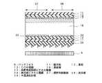
内部半透過型の一例として、特許文献1に開示された液晶表示装置が提案されている。図25は、特許文献1に記載の図1をもとに、従来の内部半透過型液晶表示素子の断面構成を模式的に示した断面図である。図25に示すように、バックライト109上には、1対の基板102が対向して配置され、基板102の対向面とは反対側の面には夫々偏光板101が設けられている。バックライト109側に配置された第1の基板の上面は、凹凸反射電極(内部反射板)120が設けられた反射部121と電極103が設けられた透過部122とからなり、この第1の基板に対向する第2の基板の対向面上には電極103が反射部120及び透過部121に亘って設けられており、2枚の基板102間には液晶層104が封止されている。即ち、このように構成された内部反射型液晶表示素子においては、1画素内に外部からの入射光を反射させるための凹凸反射電極(内部反射板)120が設けられた反射部121と、バックライト109の光を透過させるための透過部122が備えられており、反射光と透過光を共に表示に利用することができる。なお、反射部と透過部は液晶の適した厚さが異なるため、夫々の液晶厚を異ならせることが多い。図25では、反射部121における凹凸反射電極(内部反射板)120と対向する電極103との間隔が、透過部122における対向する電極103間の間隔よりも小さくなるように、反射部における基板上には絶縁膜127が設けられ、その上に凹凸反射電極(内部反射板)120が形成されている。 As an example of the internal transflective type, a liquid crystal display device disclosed in Patent Document 1 has been proposed. FIG. 25 is a cross-sectional view schematically showing a cross-sectional configuration of a conventional internal transflective liquid crystal display element based on FIG. 1 described in Patent Document 1. As shown in FIG. 25, a pair of
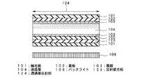
また、外部半透過型の一例として、特許文献2に開示された液晶表示装置がある。図26は、特許文献2に記載の図1をもとに、従来例の外部半透過型液晶表示素子の断面構成を模式的に示した断面図である。図26に示すように、液晶表示装置にはバックライト109が設けられており、バックライト109の上には、1対の基板102が対向して配置され、1対の基板102の対向面上には夫々電極103が設けられており、電極103間には液晶層104が挟持されている。バックライト109側に配置された基板102のバックライト109側の表面には、反射偏光板123が設けられており、更に、反射偏光板123の表面を覆うように偏光板101が設けられている。また、この基板に対向して配置された基板102のバックライト109とは反対側の面上にも偏光板101が設けられている。本従来例においては、透過表示時にはバックライト109の光で表示を行い、反射表示時には表示面側から入射した光の特定の偏光が反射偏光板123で反射され、反射光が観察者側に出射され、表示を行う。この場合、透過部と反射部は同じ箇所となり、一画素が透過部兼反射部124となる。本従来技術における反射偏光板を用いた方式では、透過表示と、反射表示の電圧−透過率(反射率)曲線が反転する特徴がある。 As an example of the external transflective type, there is a liquid crystal display device disclosed in Patent Document 2. FIG. 26 is a cross-sectional view schematically showing a cross-sectional configuration of a conventional external transflective liquid crystal display element based on FIG. 1 described in Patent Document 2. As shown in FIG. 26, a
一方、特許文献3に開示された反射偏光板を用いた表示素子においては、位相差板を使用することにより、透過表示と、反射表示の電圧−透過率(反射率)曲線が揃うことを特徴とする表示素子が記載されている。 On the other hand, in the display element using the reflective polarizing plate disclosed in
外部反射方式の別の方法を採用した液晶表示装置として、特許文献4に記載された液晶表示装置がある。図27は、特許文献4に記載の図15をもとに、従来例の外部半透過型液晶表示素子の断面構成を模式的に示した断面図である。図27に示すように、バックライト109の上方には、1対の対向する基板102が配置されており、基板の対向する表面には夫々電極103が設けられ、電極103間には液晶層104が挟持されている。また、1対の基板102の対向面側とは反対側の面上には夫々偏光板101が設けられている。バックライト109側の偏光板101のバックライト側の面上には半透過反射板125が設けられており、液晶表示素子は透過兼反射部126を構成している。即ち、本従来技術の液晶表示素子においては、バックライト109側に設けられた偏光板101とバックライト109との間に、偏光反射板ではなく、半透過反射板125が配置されている。また、この場合、特許文献2とは異なり、透過表示と反射表示の電圧−透過率(反射率)曲線が揃っている。 As a liquid crystal display device employing another method of the external reflection method, there is a liquid crystal display device described in
ところで、近時、表示装置には、それを視認している本人以外の人、即ちその近傍にいる人が見ることができないようにする秘密保護機能が求められている。例えば、ATM(Automated Teller Machine:現金自動預け払い機)として知られる金融端末等では、表示装置に表示された数字ボタンに触れて個人の暗証番号を入力する必要があり、この表示装置を他人に視認されることを避けなければならない。また、同様に携帯電話等には、表示情報を本人の近傍にいる他人から視認されることを回避できる機能が求められている。更に、PDA及びノート型パーソナルコンピュータ(以下、ノートPCという)等においても、電車等の交通機関内で使用する際には、同様に近傍にいる他人から見えないようにする機能が求められている。 By the way, recently, a display device is required to have a secret protection function that prevents a person other than the person who is viewing the display device, that is, a person in the vicinity of the display device from seeing it. For example, in a financial terminal or the like known as ATM (Automated Teller Machine), it is necessary to touch a number button displayed on the display device and input a personal code number. You must avoid being visible. Similarly, a mobile phone or the like is required to have a function that can prevent display information from being viewed by others in the vicinity of the person. Furthermore, PDAs, notebook personal computers (hereinafter referred to as notebook PCs), and the like are also required to have a function for preventing others from seeing them when they are used in transportation such as trains. .
一方で、表示装置を複数人数で視認する必要性がある場合もある。例えば、携帯電話等で画面にテレビ画像を表示するときには、その携帯電話の所有者以外に、その近傍にいる人にも見せたい場合もある。また、ノートPCのデータ画面を複数人で眺める場合もある。 On the other hand, it may be necessary to visually recognize the display device by a plurality of people. For example, when a television image is displayed on a screen with a mobile phone or the like, there are cases where it is desired to show it to a person in the vicinity in addition to the owner of the mobile phone. In some cases, the data screen of the notebook PC may be viewed by a plurality of people.
従って、表示装置としては、秘匿性の高い情報を個人で見る場合の狭視野モードと、公開性の高い情報を複数人でみる場合の広視野モードとがある。そして、携帯電話、PDA及びノートPC等においては、これらの表示モードを切り替えることが可能な表示装置が要望されている。 Accordingly, the display device includes a narrow-field mode in which highly confidential information is viewed by individuals, and a wide-field mode in which highly open information is viewed by a plurality of people. In mobile phones, PDAs, notebook PCs, and the like, there is a demand for a display device that can switch between these display modes.
出願人は、狭視野モードと広視野モードとを切り替えることができる表示装置を出願(特願2004−298571)している。図21は、この出願の際に添付した図1をもとに、液晶表示装置の断面構成を模式的に示した断面図である。図21に示すように、この液晶表示装置においては、光を面状に出射するバックライト109が設けられており、バックライト109の上にはバックライト109から入射された光の方向を規制して出射するルーバー106が設けられている。ルーバー106は、光を透過する透明領域106aと、光を吸収する吸収領域106bとが、ルーバー106表面に平行な方向に交互に配置されている。ルーバー106の上にはルーバー106から入射された光を透過する状態と散乱する状態とに切替可能の透明・散乱切替素子107が設けられている。透明・散乱切替素子107においては、高分子膜105aの中に液晶領域105bが分散した高分子分散型液晶層105が基板102の表面を覆うようにして設けられた1対の電極103間に挟まれて構成されており、高分子分散型液晶層105は、電極103間に電圧を印加しない場合には入射された光を透過する状態であり、電極103間に電圧を印加した場合には入射された光を散乱する状態になる。透明・散乱切替素子107の上には液晶パネル110が設けられている。液晶パネル110においては、透明・散乱切替素子107から入射された光を偏向する偏光板101が設けられており、偏光板101の上には基板102が設けられている。基板102の上には電極103が設けられており、電極103の表面を覆うように液晶層104が設けられている。液晶層104の上には液晶層に電圧を印加するための電極103が設けられており、この電極の上には基板102が設けられている。更に、基板102の上には液晶パネルからの出射光を偏向する偏光板101が設けられている。The applicant has applied for a display device(Japanese Patent Application No. 2004-298571) that can switch betweena narrow-field mode and a wide-field mode. Figure 21 is based on the Figure 1which is attached at the time of thisapplication, a cross-sectional view schematically showing a sectional configuration of aliquid crystal display device. As shown in FIG. 21, inthis liquid crystal display device, a
まず、狭視野モード時の動作を説明する。狭視野モード時は、透明・散乱切替素子107は透明状態である。バックライト109から出射した光は拡散光であるが、ルーバー106に入射すると、光規制方向に広がった光は吸収領域106bに吸収され、ルーバー106から出射する光は、指向性の高い分布の光となる。この指向性の高い分布の光は、透明状態にある透明・散乱切替素子107を透過し、指向性の高い分布の光を出射する。この指向性の高い分布の光が、液晶パネル110を透過して、指向性の高い分布の光を出射するため、狭視野表示となる。 First, the operation in the narrow field mode will be described. In the narrow field mode, the transparent / scattering
次に、広視野モード時の動作を説明する。広視野モード時は、透明・散乱切替素子107は散乱状態である。バックライト109から出射した光は拡散光であるが、ルーバー106に入射すると、光規制方向に広がった光は吸収領域106bに吸収され、ルーバー106から出射する光は、指向性の高い分布の光となる。この指向性の高い分布の光は、散乱状態にある透明・散乱切替素子107を透過し、均一に散乱され、指向性が低下し、広角の分布の光を出射する。広角の分布の光が、液晶パネル110を透過して、広角の分布の光を出射するため、広視野表示となる。即ち、図21に示す装置では、液晶パネルを透過する前の光の角度分布状態を変えることで、狭視野モードと広視野モードの視野角切替を行う。Next, the operation in the wide viewing mode will be described. In the wide field mode, the transparent /
また、上述とは別の方法で狭視野モードと広視野モードとを切り替えることができる表示装置として、特許文献5に開示された液晶表示装置がある。図22は、特許文献5に記載の液晶表示装置の画素構成を示す平面図である。また、図23は、同文献に記載の狭視野モード時の広視野域での電圧−透過率特性図であり、図24は、同文献に記載の広視野モード時の広視野域での電圧−透過率特性図である。Moreover, there is a liquid crystal display device disclosed in
図22に示すように、特許文献5に記載のアクティブマトリクス型液晶表示装置は、透明電極間に液晶を挟持してマトリックス状に配置された複数の画素111からなり、各画素111は制御線116に接続された第1の画素領域112と、第1の画素領域とはコンデンサ114を介して接続された第2の画素領域113とからなり、更に第1の画素領域112と第2の画素領域113との間にはスイッチング素子115が設けられている。As shown in FIG. 22, the active matrix liquid crystal display device described in
ここで、液晶モードはTN(Twisted Nematic)モードとして動作の説明をする。狭視野モード時には、スイッチング素子115をショートする。第1の画素領域112と第2の画素領域113は直接接続されるため、第1の画素領域112と第2の画素領域113には、制御線116と同電圧(V1)が供給される。第1の画素領域112における第1の画素電極と第2の画素領域113における第2の画素電極は同電圧であるので、通常のTNモードと同様に動作する。図23に示すように、第1の画素領域112と第2の画素領域113の電圧−透過率曲線を合成した画素111全体の広視野域での電圧−透過率曲線117aには、TNモードの特徴である階調反転が発生する。 Here, the operation will be described assuming that the liquid crystal mode is a TN (Twisted Nematic) mode. In the narrow field mode, the switching
一方、広視野モード時には、スイッチング素子115をオープンにする。第1の画素領域112と第2の画素領域113は、コンデンサ114を介して接続されているため、制御線116に印加した駆動電圧は、第1の画素領域112にはそのまま供給され(電圧V1)、第2の画素領域113に対してはコンデンサ114を介して供給され(電圧V2)、第1の画素領域112と第2の画素領域113の電圧は異なる電圧となる。即ち、コンデンサを介して接続される第2の画素領域113における第2の画素電圧の方が、第1の画素領域112における第1の画素電圧に比べ、電圧の絶対値は小さくなる(|V1|>|V2|)。図24に示すように、第1の画素領域112と第2の画素領域113の液晶分子に夫々異なる電圧を加えることにより、第1の画素領域112の広視野域での電圧−透過率曲線118と、第2の画素領域113の広視野域での電圧−透過率曲線119は異なった波形となり、第1の画素領域112の電圧−透過率曲線と第2の画素領域113の電圧−透過率曲線を合成した画素111全体の広視野域での電圧−透過率曲線117bは階調反転のない滑らかな曲線となる。 On the other hand, in the wide viewing mode, the switching
即ち、特許文献5に記載の技術においては、画素の電圧−透過率特性を変化させ、液晶パネルの視野角特性を変えることで、狭視野モードと広視野モードの視野角切替を行う。表1に広視野モードと狭視野モードでの、第1の画素領域と第2の画素領域とに印加される電圧の違いをまとめた。第1の画素領域と第2の画素領域の電圧は、広視野モードでは異なる電圧となり、狭視野モードでは同電圧となる。That is, in the technique described in

また、特許文献6においては、1つの画素を配向特性の異なる複数の副画素により構成し、各副画素にはその動作を独立に制御するための制御線が接続された液晶表示装置が記述されている。そして、操作者が行うスイッチ部の切替操作により、画素の中から、制御線群を通じて表示信号を印加する副画素を選択し、表示画素の視野角を、操作者から見易くする広視野角と第三者からのぞき込みにくくする狭視野角とに切り替える。
しかしながら、上述の従来技術には以下に示すような問題点がある。 However, the above-described prior art has the following problems.
図21に記載の視野角切替液晶表示装置においては、バックライトから出射される指向性の低い光をルーバーによって指向性の高い光に変換し、この指向性の高い光を透明・散乱切替素子によって透過又は散乱して、狭視野モードと広視野モードの切替を行う。そのため本手法により、透過型液晶表示装置と半透過型液晶表示装置の透過表示においては、視野角切替が可能となる。一方、半透過型液晶表示装置の反射表示においては、液晶パネル表示面側から入射した光を、内部半透過型では液晶セル内部の反射板により、また、外部半透過型では液晶セル外部の反射板により、観察者側に反射し、この光(反射表示光)で表示を行っている。内部半透過型においては、反射表示光の光路には、透明・散乱切替素子は含まれておらず、本技術による反射表示光の方向分布の変更は困難である。透明・散乱切替素子を外部反射板とバックライトの間に設けた外部半透過型においても、同様に反射表示光の方向分布の変更は困難である。透明・散乱切替素子を外部反射板と液晶パネルとの間に設けた外部半透過型においては、反射表示光の光路に、反射前後に相当して透明・散乱切替素子が2回含まれるため、透明・散乱切替素子を散乱状態にすると、反射表示光の強度が減衰し暗くなり実用的ではない。従って、反射表示部を有する半透過型液晶表示装置の視野角切替には未対応であった。In the viewing angle switching liquid crystal display deviceshown in FIG. 21 , light having low directivity emitted from a backlight is converted into light having high directivity by a louver, and the light having high directivity is converted by a transparent / scattering switching element. Transmission or scattering is performed to switch between the narrow field mode and the wide field mode. Therefore, according to the present technique, the viewing angle can be switched in the transmissive display of the transmissive liquid crystal display device and the transflective liquid crystal display device. On the other hand, in the reflective display of the transflective liquid crystal display device, the light incident from the liquid crystal panel display surface is reflected by the reflector inside the liquid crystal cell in the internal transflective type and reflected from the liquid crystal cell in the external transflective type. The light is reflected on the viewer side by the plate and displayed with this light (reflected display light). In internal transflective, the optical path of the reflected display light, transparent-scattering switching element is not included, changes direction distribution of the reflected display light according tothe present technology is difficult. Similarly, in the external transflective type in which the transparent / scattering switching element is provided between the external reflector and the backlight, it is difficult to change the direction distribution of the reflected display light. In the external transflective type in which the transparent / scattering switching element is provided between the external reflector and the liquid crystal panel, the optical path of the reflected display light includes the transparent / scattering switching element twice before and after the reflection, When the transparent / scattering switching element is in the scattering state, the intensity of the reflected display light is attenuated and darkened, which is not practical. Therefore, the viewing angle switching of the transflective liquid crystal display device having the reflective display portion is not supported.
また、特許文献5に記載の液晶表示装置においては、透過表示の狭視野角モードは、広視野角では見ている人に対して階調反転が生じている。しかし、階調反転程度では、表示によっては広視野角の観察者が視認可能であった。更に、この方式においても、反射表示の視野角切替については記載されておらず、半透過型液晶表示装置の視野角切替には未対応であった。また、特許文献6に記載の液晶表示装置においても、反射表示の視野角切替には言及しておらず、半透過型液晶表示装置の視野角切替に対応するものではではない。Further, in the liquid crystal display device described in
本発明はかかる問題点に鑑みてなされたものであって、狭視野モードと広視野モードとの視野角の切替が可能の半透過型液晶表示装置及び携帯端末装置を提供することを目的とする。 The present invention has been made in view of such problems, and an object of the present invention is to provide a transflective liquid crystal display device and a portable terminal device capable of switching the viewing angle between a narrow viewing mode and a wide viewing mode. .
本発明に係る半透過型液晶表示装置は、電極が形成された1対の基板間に液晶層が挟持された液晶パネルと、この液晶パネルに光を出射するバックライトと、前記液晶層に印加する電圧を制御する制御部と、を有し、前記液晶パネルの各画素は個別に、表示面側からの入射光を反射して表示する反射部と、前記バックライトから出射した光を透過させて表示する透過部とを有し、前記反射部と前記透過部は共に広視野角特性を有し、特定角度以上の広視野角領域では前記反射部の輝度は前記透過部の輝度より大きく、その他の角度領域では前記透過部の輝度は前記反射部の輝度より大きい輝度視野角特性を有し、前記制御部は前記液晶層に印加する電圧を前記反射部及び前記透過部に対して独立に制御して、広視野モード時には、反射部が通常表示又は暗表示を行うと共に、透過部が通常表示を行い、狭視野モード時には、反射部が偽情報表示を行うと共に、透過部が通常表示を行うように制御することにより、広視野モードと狭視野モードとの視野角切替を行うことを特徴とする。 A transflective liquid crystal display device according to the present invention includes a liquid crystal panel in which a liquid crystal layer is sandwiched between a pair of substrates on which electrodes are formed, a backlight that emits light to the liquid crystal panel, and an application to the liquid crystal layer A control unit that controls a voltage to be transmitted, and each pixel of the liquid crystal panel individually reflects and displays incident light from the display surface side, and transmits light emitted from the backlight. The reflective part and the transmissive part both have a wide viewing angle characteristic, and the brightness of the reflective part is greater than the brightness of the transmissive part in a wide viewing angle region above a specific angle, In other angle regions, the luminance of the transmissive part has a luminance viewing angle characteristic larger than that of the reflective part, and the control unit applies a voltage applied to the liquid crystal layer independently to the reflective part and the transmissive part. Control and allow the reflector to pass In addition to performing display or dark display, the transmission unit performs normal display, and in the narrow-field mode, the reflection unit performs false information display and the transmission unit performs control so that normal display is performed. The viewing angle is switched to the viewing mode.
狭視野モード時には、画素の一部の反射部では偽情報表示を行わず、通常表示又は暗表示を行うことで画像パターンの表示を行ってもよい。狭視野モード時には、広視野角から視認可能な画像パターンを表示することで、何も見えない場合に比べ、ファッション性を高めることが出来る。 In the narrow-field mode, the image pattern may be displayed by performing normal display or dark display instead of performing false information display at some of the reflective portions of the pixels. By displaying an image pattern that can be viewed from a wide viewing angle in the narrow viewing mode, the fashionability can be improved compared to the case where nothing can be seen.
また、画像パターンの表示は、空間的、時間的、又は時空間的に変動させることが好ましい。これにより、目が慣れることで、本来の表示内容が視認可能となることを防ぐことができる。 The display of the image pattern is preferably varied spatially, temporally, or spatiotemporally. Thereby, it is possible to prevent the original display contents from being visually recognized by getting used to the eyes.
反射部に形成された反射ピクセル電極と、透過部に形成された透過ピクセル電極とを分離して設け、夫々異なるTFT(Thin Film Transistor:薄膜トランジスタ)に接続することで、反射部及び透過部における液晶層に印加する電圧を独立に制御することができる。 The reflective pixel electrode formed in the reflective portion and the transmissive pixel electrode formed in the transmissive portion are separately provided and connected to different TFTs (Thin Film Transistors), so that the liquid crystal in the reflective portion and the transmissive portion is provided. The voltage applied to the layer can be controlled independently.
反射部に形成されたCOM電極と、透過部に形成されたCOM電極とを分離して設けることで、反射部及び透過部における液晶層に印加する電圧を独立に制御することができる。 By separately providing the COM electrode formed in the reflection part and the COM electrode formed in the transmission part, the voltage applied to the liquid crystal layer in the reflection part and the transmission part can be controlled independently.
本発明に係る半透過型液晶表示装置は、電極が形成された1対の基板間に液晶層が挟持された液晶パネルと、この液晶パネルに光を出射するバックライトと、前記バックライト側に配置された基板のバックライト側の面上に設けられた反射偏光板又は半透過反射板と、前記液晶層に印加する電圧を制御する制御部と、を有し、前記液晶パネルの各画素は、個別に第1表示部と第2表示部とを有し、前記第1表示部及び前記第2表示部は共に広視野角特性を有し、特定角度以上の広視野角領域では前記第1表示部の輝度は前記第2表示部の輝度より大きく、その他の角度領域では前記第2表示部の輝度は前記第1表示部の輝度より大きい輝度視野角特性を有し、前記制御部は前記液晶層に印加する電圧を前記第1表示部及び前記第2表示部に対して独立に制御して、広視野モード時には、第1表示部が通常表示又は暗表示を行うと共に、第2表示部が通常表示を行い、狭視野モード時には、第1表示部が偽情報表示を行うと共に、第2表示部が通常表示を行うように制御することにより、広視野モードと狭視野モードとの視野角切替を行うことを特徴とする。 A transflective liquid crystal display device according to the present invention includes a liquid crystal panel in which a liquid crystal layer is sandwiched between a pair of substrates on which electrodes are formed, a backlight that emits light to the liquid crystal panel, and the backlight side. A reflective polarizing plate or a transflective plate provided on the backlight side surface of the substrate disposed, and a control unit for controlling a voltage applied to the liquid crystal layer, and each pixel of the liquid crystal panel Each of the first display unit and the second display unit, both of the first display unit and the second display unit have wide viewing angle characteristics, and the first display unit has a wide viewing angle region of a specific angle or more. The luminance of the display unit is larger than the luminance of the second display unit, and the luminance of the second display unit is larger than the luminance of the first display unit in other angular regions, and the control unit A voltage applied to the liquid crystal layer is applied to the first display unit and the second display unit. In the wide field mode, the first display unit performs normal display or dark display, and the second display unit performs normal display. In the narrow field mode, the first display unit displays false information. In addition, the viewing angle is switched between the wide viewing mode and the narrow viewing mode by controlling the second display unit to perform normal display.
また、狭視野モード時には、画素の一部の第1表示部では偽情報表示を行わず、通常表示又は暗表示を行うことで画像パターンの表示を行ってもよい。狭視野モード時には、広視野角から視認可能な画像パターンを表示することで、何も見えない場合に比べ、ファッション性を高めることが出来る。更にまた、狭視野モード時の画像パターンの表示は、空間的、時間的、又は時空間的に変動させることが好ましい。これにより、目が慣れることで、本来の表示内容が視認可能となることを防ぐことができる。 In the narrow-field mode, the image pattern may be displayed by performing normal display or dark display instead of performing false information display on the first display portion of a part of the pixels. By displaying an image pattern that can be viewed from a wide viewing angle in the narrow viewing mode, the fashionability can be improved compared to the case where nothing can be seen. Furthermore, it is preferable that the display of the image pattern in the narrow field mode is varied spatially, temporally, or spatiotemporally. Thereby, it is possible to prevent the original display contents from being visually recognized by getting used to the eyes.
また、第1表示部に形成された第1ピクセル電極と、第2表示部に形成された第2ピクセル電極とを分離して設け、夫々異なるTFTに接続することで、第1表示部及び第2表示部における液晶層に印加する電圧を独立に制御することができる。また、第1表示部に形成されたCOM電極と、第2表示部に形成されたCOM電極とを分離して設けることで、第1表示部及び第2表示部における液晶層に印加する電圧を独立に制御することができる。 In addition, the first pixel electrode formed in the first display portion and the second pixel electrode formed in the second display portion are provided separately, and are connected to different TFTs, respectively. The voltage applied to the liquid crystal layer in the two display units can be controlled independently. Further, by providing the COM electrode formed on the first display unit and the COM electrode formed on the second display unit separately, the voltage applied to the liquid crystal layer in the first display unit and the second display unit can be increased. It can be controlled independently.
偽情報は、白輝度、中間輝度、又は偽色光のいずれを利用してもよい。偽情報は、特定の視野角以上に対して本来の表示内容が視認不可となる表示であればよい。偽情報を表示させることにより、狭視野モード時には、反射光により広視野角から本来の表示内容が視認されることがない。 The false information may use any of white luminance, intermediate luminance, or false color light. The false information only needs to be a display in which the original display content is not visible for a specific viewing angle or more. By displaying the false information, the original display content is not visually recognized from the wide viewing angle by the reflected light in the narrow viewing mode.
また、観測者側にフロントライトを設けることができる。これにより、外光が存在しないか、又は弱い場合でも、フロントライトにより十分な輝度が得られ、視野角の切替が機能する。 In addition, a front light can be provided on the observer side. Thereby, even when external light is not present or weak, sufficient luminance is obtained by the front light, and switching of the viewing angle functions.
バックライトから入射された光の方向を規制して出射するルーバーを設けて使用することができる。これにより、透過部における狭視野の視野角特性を向上させることが可能となる。 A louver that emits light while regulating the direction of light incident from the backlight can be provided. Thereby, it is possible to improve the viewing angle characteristics of the narrow field of view in the transmission part.
また、入射光を透過する状態と散乱する状態とに切替可能の透明・散乱切替素子を設けて使用することができる。これにより、透過部は透明・散乱切替素子により視野角の切替が可能となり、反射部の表示切替も併用することで、効率的な視野角の切替が可能となる。 Further, a transparent / scattering switching element that can be switched between a state of transmitting incident light and a state of scattering of incident light can be provided and used. Thereby, the viewing angle of the transmissive part can be switched by the transparent / scattering switching element, and the viewing angle of the transmissive part can be efficiently switched by using the display switching of the reflecting part together.
本発明においては、携帯端末装置に、前記半透過型液晶表示装置を使用することにより、使用者が携帯端末装置の使用環境に合わせて、最適な表示状態を設定することができる。In the present invention, by using the transflective liquid crystal display device for the mobile terminal device, the user can set an optimal display state according to the usage environment of the mobile terminal device.
本発明によれば、液晶表示素子の各画素内に個別に反射部及び透過部を設け、反射部及び透過部における液晶層に印加する電圧を独立に制御することにより、広視野モードと狭視野モードとの視野角切替が可能の半透過型液晶表示装置を提供することができる。また、液晶表示素子が反射部兼透過部である外部半透過型液晶表示装置に対しても、各画素内に個別に反射表示を主に使用する第1表示部と、透過表示を主に使用する第2表示部とを設け、第1表示部及び第2表示部における液晶層に印加する電圧を独立に制御することにより、広視野モードと狭視野モードとの視野角切替が可能の半透過型液晶表示装置を提供することができる。本発明により、従来未対応であった反射表示部を有する半透過型液晶表示装置の視野角切替が可能となる。 According to the present invention, a wide-field mode and a narrow-field mode are provided by separately providing a reflective portion and a transmissive portion in each pixel of the liquid crystal display element, and independently controlling the voltage applied to the liquid crystal layer in the reflective portion and the transmissive portion. A transflective liquid crystal display device capable of switching the viewing angle with the mode can be provided. In addition, for an external transflective liquid crystal display device in which the liquid crystal display element is a reflective and transmissive part, a first display part that mainly uses reflective display in each pixel and a transmissive display are mainly used. And a semi-transmission capable of switching the viewing angle between the wide viewing mode and the narrow viewing mode by independently controlling the voltage applied to the liquid crystal layer in the first display portion and the second display portion. Type liquid crystal display device can be provided. According to the present invention, it is possible to switch the viewing angle of a transflective liquid crystal display device having a reflective display portion which has not been conventionally supported.
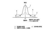
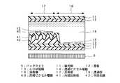
以下、本発明の実施形態に係る半透過型液晶表示装置及び携帯端末装置について図面を参照して詳細に説明する。先ず、本発明の第1の実施形態に係る半透過型液晶表示装置について説明する。図4は、第1の実施形態に係る内部半透過型の液晶表示装置の断面図であり、また、図5は、第1の実施形態におけるTFT基板側電極と対向基板側電極の概略図である。更に、表2は、第1の実施形態の広視野モード及び狭視野モードにおける反射部及び透過部の第1の動作説明図であり、表3は、第1の実施形態の広視野モード及び狭視野モードにおける反射部及び透過部の第2の動作説明図である。また、図1は、第1の実施形態における狭視野モード時の視野角−輝度特性を示す曲線である。 Hereinafter, a transflective liquid crystal display device and a mobile terminal device according to an embodiment of the present invention will be described in detail with reference to the drawings. First, a transflective liquid crystal display device according to a first embodiment of the present invention will be described. FIG. 4 is a cross-sectional view of the internal transflective liquid crystal display device according to the first embodiment, and FIG. 5 is a schematic diagram of the TFT substrate side electrode and the counter substrate side electrode in the first embodiment. is there. Further, Table 2 is a first operation explanatory diagram of the reflection part and the transmission part in the wide-field mode and the narrow-field mode of the first embodiment, and Table 3 is the wide-field mode and the narrow-field of the first embodiment. It is 2nd operation | movement explanatory drawing of the reflection part in a visual field mode, and a transmission part. FIG. 1 is a curve showing viewing angle-luminance characteristics in the narrow viewing mode in the first embodiment.
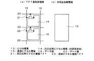
先ず、本発明の第1の実施形態に係る半透過型液晶表示装置の1画素の構成を図4及び図5を用いて説明する。図4に示すように、バックライト6の上部には一対の基板12が対向して配置されており、バックライト光の出射方向である観察者側に配置された基板12のバックライト6側の面上には、COM電極13が設けられている(この基板を対向基板という)。また、バックライト6側に配置された基板12の対向基板側の面上には、表面が凹凸形状をなし観察者側から入射する光を反射する凹凸反射ピクセル電極(内部反射板)14と、バックライト6から出射された光を透過させる透過ピクセル電極15とが分離して設けられている(この基板をTFT基板という)。このように、本実施形態における液晶表示装置の液晶パネルは、凹凸反射ピクセル電極(内部反射板)14が設けられた反射部17と透過ピクセル電極15が設けられた透過部18とからなる。2枚の基板間には液晶層16が挟持されているが、反射部17と透過部18とでは夫々最適な液晶厚が異なるために、TFT基板に沿って段差が設けられており、凹凸反射ピクセル電極14とこれに対置するCOM電極13との間隔は、透過ピクセル電極15とこれに対置するCOM電極13との間隔よりも小さく、反射部17の液晶厚が薄くなっている。なお、図4では、段差はTFT基板に作製されているが、対向基板に設けても良い。対向基板とTFT基板は、液晶層16を挟持して貼り合わされており、対向基板とTFT基板の対向面側とは反対の面上には、夫々偏光板11が設けられている。 First, the configuration of one pixel of the transflective liquid crystal display device according to the first embodiment of the present invention will be described with reference to FIGS. As shown in FIG. 4, a pair of
図5(a)は、TFT基板側電極の平面概略図であり、図4に示すTFT基板上の電極の構造を基板上面側から図示したものである。図5(a)に示すように、格子状に設けられたデータ線19とゲート線20とにより区画された異なる領域に、夫々凹凸反射ピクセル電極(内部反射板)14と透過ピクセル電極15とが配置されている。凹凸反射ピクセル電極(内部反射板)14が配置された区画のデータ線19とゲート線20の交点付近には凹凸反射ピクセル電極TFT21が形成され、凹凸反射ピクセル電極(内部反射板)14は凹凸反射ピクセル電極TFT21のソース電極に接続される。同様に、透過ピクセル電極15が配置された区画のデータ線19とゲート線20の交点付近には透過ピクセル電極TFT22が形成され、透過ピクセル電極15は透過ピクセル電極TFT22のソース電極に接続される。即ち、凹凸反射ピクセル電極(内部反射板)14の配置された反射部17と透過ピクセル電極15が配置された透過部18に夫々異なる電圧を印加可能とするため、凹凸反射ピクセル電極14と透過ピクセル電極15には、夫々異なるTFTが接続されている。また、図5(b)は対向基板側電極の平面概略図である。図5に示すように、対向基板側のCOM電極13は、反射部17と透過部18に対して共通である。 FIG. 5A is a schematic plan view of the TFT substrate side electrode, and illustrates the structure of the electrode on the TFT substrate shown in FIG. 4 from the upper surface side of the substrate. As shown in FIG. 5 (a), a concavo-convex reflective pixel electrode (internal reflector) 14 and a
次に、第1の実施形態の動作について、図4、表2、及び図1を用いて説明する。本発明の半透過型液晶表示装置を用いて表示を行う場合、反射部17においては、観察者側から表示面に入射した光は液晶層16を通過後、凹凸反射ピクセル電極(内部反射板)14により反射され、再び液晶層16を通過し、表示面から出射して表示光となる。一方、透過部18においては、バックライト6から出射された光は、透過ピクセル電極15を通過し、液晶層16を通過した後、表示面から出射して表示光となる。このとき、反射部17及び透過部18における電極間の電圧を独立に制御することにより、反射部17及び透過部18における液晶の配向を制御することができ、表示状態の制御が可能となる。また、透過部は単独で広視野表示が可能な広視野の視野角特性を有する。 Next, the operation of the first embodiment will be described with reference to FIG. 4, Table 2, and FIG. In the case of performing display using the transflective liquid crystal display device of the present invention, the light incident on the display surface from the viewer side in the
表2に示すように、広視野モード時は、透過部は通常表示を行い、反射部も通常表示を行う。一方、狭視野モード時は、透過部は通常表示であるが、反射部は明状態(白表示)にする。そのとき、図1に示すように、特定の視野角以上に対して(即ち、視野角を制限した範囲3)、反射部の輝度2が透過部の輝度1より大きくなるように設計することで、視野角を制限した範囲3では、透過部の表示内容が視認不可となる。即ち、反射部は視野角制御部、透過部は表示部と表現することができる。従って、反射部(視野角制御部)の表示切替により、広視野モードと狭視野モードの視野角切替が可能となる。 As shown in Table 2, in the wide viewing mode, the transmissive part performs normal display and the reflective part also performs normal display. On the other hand, in the narrow field mode, the transmissive part is normally displayed, but the reflective part is in a bright state (white display). At that time, as shown in FIG. 1, the luminance 2 of the reflection part is designed to be larger than the luminance 1 of the transmission part for a specific viewing angle or more (that is, the
なお、狭視野モード時の反射部は、R(赤)G(緑)B(青)3画素の明状態(白表示)に限らず、中間輝度又は偽色表示でも良く、視野角を制限した範囲3内で、透過部の表示内容が視認不可となれば良い。 In addition, the reflection part at the time of the narrow-field mode is not limited to the bright state (white display) of R (red), G (green), and B (blue) three pixels, but may be intermediate luminance or false color display, and the viewing angle is limited. Within the
また、第1の実施形態において、表3に示すように、広視野モード時は、透過部は通常表示を行い、反射部は暗表示(黒表示)を行ってもよい。表2の場合には、広視野モード時は、反射部では通常表示を行っているので、外光による表示内容の視認が可能であるが、表3の場合には、広視野モード時は、反射部は通常表示は行っておらず、外光による表示内容の視認は困難である。 In the first embodiment, as shown in Table 3, in the wide viewing mode, the transmissive part may perform normal display and the reflective part may perform dark display (black display). In the case of Table 2, in the wide viewing mode, since the normal display is performed in the reflecting portion, the display contents can be visually recognized by external light. In the case of Table 3, in the wide viewing mode, The reflection part does not normally display, and it is difficult to visually recognize the display content by external light.
垂直電界で動作させる液晶のモードは、広視野角なVA(Vertical Alignment:ヴァーティカル・アライメント)モードが好ましい。VAモードではマルチドメイン化され視野角依存性が低減されたMVA(Multi-domain Vertical Alignment:マルチドメイン・ヴァーティカル・アライメント)方式、PVA(Patterned Vertical Alignment:パターンド・ヴァーティカル・アライメント)方式、及びASV(Advanced Super V:アドヴァンスト・スーパー・ヴイ)方式等が挙げられる。更に、本発明はフィルム補償TNモードの液晶表示パネルにも好適に使用することができる。 The mode of the liquid crystal operated in a vertical electric field is preferably a VA (Vertical Alignment) mode with a wide viewing angle. In VA mode, MVA (Multi-domain Vertical Alignment) method, PVA (Patterned Vertical Alignment) method with multi-domain and reduced viewing angle dependence, and ASV (Advanced Super V: Advanced Super Vui) method etc. are mentioned. Further, the present invention can be suitably used for a film compensation TN mode liquid crystal display panel.
次に、本発明の第2の実施形態について説明する。第1の実施形態においては、TFT基板上の反射部及び表示部のピクセル電極が夫々異なるTFTに接続され、反射部及び表示部の電圧は独立に制御可能であった。本発明の第2の実施形態は、TFT基板上の反射部及び表示部のピクセル電極は共通であり、1つのTFTで制御されており、一方、対向基板上の反射部のCOM電極及び表示部のCOM電極が分離されている。図6は、第2の実施形態に係る内部半透過型の液晶表示装置の断面図である。また、図7は、第2の実施形態におけるTFT基板側電極と対向基板側電極の概略図である。 Next, a second embodiment of the present invention will be described. In the first embodiment, the pixel electrodes of the reflective portion and the display portion on the TFT substrate are connected to different TFTs, and the voltages of the reflective portion and the display portion can be controlled independently. In the second embodiment of the present invention, the pixel electrode of the reflective part and the display part on the TFT substrate is common and is controlled by one TFT, while the COM electrode and the display part of the reflective part on the counter substrate are controlled. The COM electrodes are separated. FIG. 6 is a cross-sectional view of an internal transflective liquid crystal display device according to the second embodiment. FIG. 7 is a schematic view of the TFT substrate side electrode and the counter substrate side electrode in the second embodiment.
第2の実施形態の構成を図6及び図7を用いて説明する。なお、図6においては、図4と同様の構成物には同一の符号を付し、又、図7においても、図5と同様の構成物には同一の符号を付してその詳細な説明は省略する。図6に示すように、基板12上に設けられた凹凸反射ピクセル電極(内部反射板)14は、透過ピクセル電極15とショートしており、一つのピクセル電極25を構成している。従って、図7(a)に示すように、ピクセル電極25に接続されるTFTはピクセル電極TFT26一つで良い。一方、図6及び図7に示すように、対向基板側は、反射部17と透過部18の夫々に対して、反射部COM電極23と透過部COM電極24とに分かれてCOM電極が形成されており、夫々異なる電圧が印加可能である。 The configuration of the second embodiment will be described with reference to FIGS. In FIG. 6, the same components as those in FIG. 4 are denoted by the same reference numerals, and also in FIG. 7, the same components as those in FIG. Is omitted. As shown in FIG. 6, the uneven reflection pixel electrode (internal reflection plate) 14 provided on the
このように、反射部COM電極23と透過部COM電極24が分離していることから、反射部と透過部の電圧を独立に制御することが可能で、第1実施形態と同様の動作が実現される。 As described above, since the reflection
次に、本発明の第3の実施形態について説明する。第1の実施形態では垂直電界で液晶を動作させるモードであったが、本発明の第3の実施形態は、横電界で液晶を動作させるモードである点が異なる。図8は、第3の実施形態に係る内部半透過型の液晶表示装置の断面図である。また、図9は、第3の実施形態におけるTFT基板側電極の概略図である。 Next, a third embodiment of the present invention will be described. In the first embodiment, the liquid crystal is operated in a vertical electric field. However, the third embodiment of the present invention is different in that the liquid crystal is operated in a horizontal electric field. FIG. 8 is a cross-sectional view of an internal transflective liquid crystal display device according to the third embodiment. FIG. 9 is a schematic view of the TFT substrate side electrode in the third embodiment.
第3の実施形態の構成を図8及び図9を用いて説明する。なお、図8においては、図4と同様の構成物には同一の符号を付し、その詳細な説明は省略する。図8に示すように、バックライト6上には液晶パネルが設けられ、バックライト6側に配置された基板12上は、内部反射板41が形成された反射部17と、バックライトが出射した光を透過させる透過部18とからなる。基板に水平な方向の横電界で動作するIPS(In Plane Switching)モードでは、液晶界面が平坦な方が好ましいので、内部反射板41上には平坦化膜42が成膜されている。更に、平坦化膜42上には、反射ピクセル電極40及びCOM電極13が櫛歯状に形成されており、また、透過部18における基板12上には、透過ピクセル電極15及びCOM電極13が櫛歯状に形成されている。これらの電極の構造を基板上面から平面視したものが図9である。図9に示すように、反射部17及び透過部18は格子状に設けられたデータ線19とゲート線20により区画されており、夫々の領域には、電極が櫛歯状に形成されている。本実施形態においては、反射部17と透過部18のCOM電極13は同電位であるが、反射ピクセル電極40と透過ピクセル電極15は、夫々反射ピクセル電極TFT21と透過ピクセル電極TFT22に接続されており、反射部17と透過部18の電圧を独立に制御可能である。反射部と透過部の電圧を独立に制御することが可能であるため、第1実施形態と同様の動作が実現される。 The configuration of the third embodiment will be described with reference to FIGS. In FIG. 8, the same components as those in FIG. 4 are denoted by the same reference numerals, and detailed description thereof is omitted. As shown in FIG. 8, a liquid crystal panel is provided on the
なお、電極の構成・配置は多少異なるが、同様な形態である、FFS(Fringe Field Switching:フリンジ・フィールド・スイッチング)方式及びAFFS(Advanced Fringe Field Switching:アドヴァンスト・フリンジ・フィールド・スイッチング)方式等も好適に使用することができる。 The configuration and arrangement of the electrodes are slightly different, but the FFS (Fringe Field Switching) method and the AFFS (Advanced Fringe Field Switching) method are the same. Can also be suitably used.
次に、本発明の第4の実施形態について説明する。第3の実施形態では、反射部と表示部のピクセル電極に夫々TFTを有していたのに対し、本発明の第4の実施形態は、反射部と表示部のピクセル電極は共通で、反射部のCOM電極と表示部のCOM電極が分かれている点が異なる。図10は、第4の実施形態に係る内部半透過型の液晶表示装置の断面図である。また、図11は、第4の実施形態におけるTFT基板側電極の概略図である。 Next, a fourth embodiment of the present invention will be described. In the third embodiment, the pixel electrodes of the reflective part and the display part have TFTs, respectively, whereas in the fourth embodiment of the present invention, the pixel electrode of the reflective part and the display part is common, The difference is that the COM electrode of the part and the COM electrode of the display part are separated. FIG. 10 is a cross-sectional view of an internal transflective liquid crystal display device according to the fourth embodiment. FIG. 11 is a schematic view of the TFT substrate side electrode in the fourth embodiment.
第4の実施形態の構成を図10及び図11を用いて説明する。なお、図10においては、図8と同様の構成物には同一の符号を付し、その詳細な説明は省略する。図10に示すように、基板に水平な方向の横電界で動作するIPS(In Plane Switching)モードでは、液晶界面が平坦な方が好ましいので、内部反射板41上には平坦化膜42が成膜されている。更に、平坦化膜42上には、ピクセル電極25及び反射部COM電極23が櫛歯状に形成されており、また、透過部18における基板12上には、ピクセル電極25及び透過部COM電極24が櫛歯状に形成されている。これらの電極の構造を基板上面から平面視したものが図11である。図11に示すように、ピクセル電極25は、単一のピクセル電極TFT26により接続されている。一方、COM電極は、反射部17と透過部18の夫々に対して、反射部COM電極23と透過部COM電極24に分かれており、別々の電圧が印加可能である。反射部と透過部の電圧を独立に制御することが可能であるため、第1実施形態と同様の動作が実現される。 The configuration of the fourth embodiment will be described with reference to FIGS. In FIG. 10, the same components as those in FIG. 8 are denoted by the same reference numerals, and detailed description thereof is omitted. As shown in FIG. 10, in an IPS (In Plane Switching) mode that operates in a horizontal electric field in a direction horizontal to the substrate, it is preferable that the liquid crystal interface is flat. Therefore, a
次に、本発明の第5の実施形態について説明する。第1乃至第4の実施形態では、狭視野モード時に、視野角制御部に偽情報を表示し、視野角制御部の偽情報により、特定の視野角以上では、表示部の表示内容を視認不可としていたのに対し、本発明の第5の実施形態では、視野角制御部と表示部の視野角特性を変え、広視野モード時には、視野角制御部と表示部は通常表示を行い、狭視野モード時には、視野角制御部は暗表示にし、狭視野特性の表示部では通常表示することより、視野角切替を行う点が異なる。図2は、第5の実施形態に係る内部半透過型の液晶表示装置の断面図である。また、表4は、第5の実施形態の広視野モードと狭視野モードにおける、反射部と透過部の動作説明図である。 Next, a fifth embodiment of the present invention will be described. In the first to fourth embodiments, false information is displayed on the viewing angle control unit in the narrow viewing mode, and the display content on the display unit is not visible at a certain viewing angle or more by the false information of the viewing angle control unit. On the other hand, in the fifth embodiment of the present invention, the viewing angle characteristics of the viewing angle control unit and the display unit are changed, and in the wide viewing mode, the viewing angle control unit and the display unit perform normal display, and the narrow viewing field. In the mode, the viewing angle control unit is dark-displayed, and the display unit with narrow viewing characteristics is normally displayed, so that the viewing angle is switched. FIG. 2 is a cross-sectional view of an internal transflective liquid crystal display device according to the fifth embodiment. Table 4 is an explanatory diagram of the operation of the reflection part and the transmission part in the wide field mode and the narrow field mode of the fifth embodiment.
第5の実施形態の構成について、図2を参照して説明する。図2(a)に示すように、本実施形態に係る半透過型液晶表示装置においては、バックライト6が設けられており、バックライト6の上には、内部半透過型液晶パネル4が配置されている。内部半透過型液晶表示装置の各画素内には内部反射板5が設けられた反射部とバックライトから出射した光が透過する透過部が設けられており、反射部と透過部とでは異なった電圧が印加可能である。更に、反射部は単独で広視野モードが可能な広視野の視野角特性を有し、透過部は単独で狭視野モードが可能な狭視野の視野角特性を有する。 The configuration of the fifth embodiment will be described with reference to FIG. As shown in FIG. 2A, in the transflective liquid crystal display device according to the present embodiment, a
表4に示すように、広視野モード時は、反射部と透過部で通常表示を行う。図2(a)に示すように、反射部において内部反射板5により反射された反射表示光8は広視野の視野角特性を持ち、バックライト6から出射され液晶パネルを透過する透過表示光7は狭視野の視野角特性を持つ。この反射表示光8と透過表示光7が合成され、広視野の視野角特性になる。一方、表4に示すように、狭視野モード時は、反射部は暗表示にし、透過部で通常表示を行う。この場合、図2(b)に示すように、透過部の狭視野表示の視野角特性のみで表示を行うため、狭視野の視野角特性が実現される。従って、反射部の表示切替で、広視野モードと狭視野モードの視野角切替が可能となる。なお、反射部の視野角特性は、透過部の狭視野と合成したときに、広視野となる特性で有れば良い。本実施形態では、広視野モードと狭視野モードで通常表示を行う透過部を表示部として、また、視野角切替に用いる反射部を視野角制御部として読み替え可能である。なお、反射部の視野角特性は、反射板の設計により任意の特性が得られる。透過部の狭視野の視野角特性は、指向性の高いバックライト又はルーバー等を使用することにより得られる。 As shown in Table 4, in the wide viewing mode, normal display is performed by the reflection part and the transmission part. As shown in FIG. 2A, the reflected
次に、本発明の第6の実施形態について説明する。第5の実施形態では反射部は広視野の視野角特性を有し、透過部は狭視野の視野角特性を有していたのに対し、第6の実施形態は、反射部は狭視野の視野角特性を有し、透過部は広視野の視野角特性を有する点が異なる。図3は、第6の実施形態に係る内部半透過型の半透過型液晶表示装置の断面図である。また、表5は、第6の実施形態の広視野モード及び狭視野モードにおける、反射部及び透過部の動作説明図である。 Next, a sixth embodiment of the present invention will be described. In the fifth embodiment, the reflecting portion has a wide viewing angle characteristic, and the transmissive portion has a narrow viewing angle characteristic. In the sixth embodiment, the reflecting portion has a narrow viewing angle. It has a viewing angle characteristic, and the transmission part is different in that it has a wide viewing angle characteristic. FIG. 3 is a cross-sectional view of an internal transflective liquid crystal display device according to the sixth embodiment. Table 5 is an explanatory diagram of the operation of the reflection part and the transmission part in the wide-field mode and the narrow-field mode of the sixth embodiment.
本実施形態に係る半透過型液晶表示装置は、1画素内に反射部と透過部が設けられており、反射部と透過部には異なる電圧が印加可能である。更に、反射部は狭視野表示の視野角特性を有し、透過部は広視野の視野角特性を有する。表5に示すように、広視野モード時は、反射部と透過部で通常表示を行う。図3(a)に示すように、反射部において内部反射板5により反射された反射表示光10は狭視野表示の視野角特性を有し、バックライト6から出射され液晶パネルを透過する透過表示部の透過表示光9は広視野表示の視野角特性を有する。この反射表示光10と透過表示光9が合成され、広視野モードの視野角特性になる。一方、表5に示すように、狭視野モード時は、反射部は通常表示を行い、透過部は暗表示にする。図3(b)に示すように、反射部の狭視野の視野角特性のみで表示を行うので、狭視野モードの視野角特性になる。従って、透過部の表示切替により、広視野モードと狭視野モードの視野角切替が可能となる。本実施形態においては、広視野モードと狭視野モードで通常表示を行う反射部は表示部として、視野角切替に用いる透過部は視野角制御部として読み替え可能である。 In the transflective liquid crystal display device according to this embodiment, a reflective portion and a transmissive portion are provided in one pixel, and different voltages can be applied to the reflective portion and the transmissive portion. Furthermore, the reflection part has a viewing angle characteristic of a narrow field display, and the transmission part has a viewing angle characteristic of a wide field of view. As shown in Table 5, in the wide viewing mode, normal display is performed by the reflection part and the transmission part. As shown in FIG. 3A, the reflected display light 10 reflected by the
次に、本発明の第7の実施形態について説明する。本実施形態は、バックライトとバックライト側偏光板との間に、透明・散乱切替素子及びルーバーを設けている。図12は、第7の実施形態に係る内部半透過型の半透過型液晶表示装置の断面図である。 Next, a seventh embodiment of the present invention will be described. In the present embodiment, a transparent / scattering switching element and a louver are provided between the backlight and the backlight-side polarizing plate. FIG. 12 is a cross-sectional view of an internal transflective liquid crystal display device according to the seventh embodiment.
図12に示すように、バックライト6が設けられており、バックライト6の上には、バックライト6から入射された光の方向を規制して出射するルーバー30が設けられている。ルーバー30は、光を透過する透明領域30aと、光を吸収する吸収領域30bとが、ルーバー30表面に平行な方向に交互に配置されている。ルーバー30の上にはルーバー30から入射された光を透過する状態と散乱する状態とに切替可能の透明・散乱切替素子31が設けられている。透明・散乱切替素子31においては、高分子膜29aの中に液晶領域29bが分散した高分子分散型液晶29が基板27の表面を覆うようにして設けられた1対の電極28間に挟持されている。透明・散乱切替素子31の上には液晶パネルが設けられており、その構成は、例えば、第1の実施形態における液晶パネルと同じであり、図4に示す液晶パネルと同じ符号を付して説明は省略する。本実施形態においては、透明・散乱切替素子31及びルーバー6を設けたことにより、視野角切替は、反射部17の表示に関わらず可能となっている。即ち、第1乃至第4の実施形態においては、反射部の偽情報表示は外光が存在しないか、又は外光が弱い場合には十分な輝度が得られず、視野角切替が機能しない場合もあるが、本実施の形態においては、上述した出願(特願2004−298571)の際に添付した明細書等に記載された方法を利用することにより、このような場合に対しても、視野角切替が可能となる。As shown in FIG. 12, a
また、広視野モード時は、反射部17は通常表示又は暗表示を行い、透過部18は広視野(透明・散乱切替素子31で切替)で通常表示を行い、狭視野モード時は、反射部17は暗表示を行い、透過部18は狭視野(透明・散乱切替素子31で切替)で通常表示を行う方法によっても、視野角切替が可能となる。 Further, in the wide field mode, the
即ち、特願2004−298571に係る発明においては、狭視野モード時には、反射表示光により表示内容が視認される可能性があったが、本発明の第7の実施の形態により、狭視野モード時に反射表示光による表示内容の視認は防げる。That is, in theinvention according to Japanese Patent Application No. 2004-298571, there is a possibility that the display content is visuallyrecognized by the reflected display light in the narrow-field mode. However, according to the seventh embodiment of the present invention, It is possible to prevent the display contents from being visually recognized by the reflected display light.
次に、本発明の第8の実施形態について説明する。第8の実施形態においては、観察者側にフロントライトを設けている。図13は、第8の実施形態に係る内部半透過型の半透過型液晶表示装置の断面図である。図13に示すように、バックライト6が設けられており、バックライト6の上には、例えば、第1の実施形態における液晶パネルが配置されている。そして、液晶パネルの上にはフロントライト32が設けられており、液晶パネルに光を入射する。第1乃至第6の実施形態においては、反射部の通常表示・明表示は、外光が存在しないか、又は外光が弱い場合には、十分な輝度が得られず、視野角切替が機能しない場合もあるが、フロントライト32を設けたことにより、そのような場合に対しても、フロントライト32により十分な輝度が得られ、視野角切替が機能する。 Next, an eighth embodiment of the present invention will be described. In the eighth embodiment, a front light is provided on the viewer side. FIG. 13 is a cross-sectional view of an internal transflective liquid crystal display device according to the eighth embodiment. As shown in FIG. 13, a
また、視野角制御部が反射部で偽色を表示するときには、フロントライトは白色光でなく、視野角制御部で表示する偽色と同等の偽色光であっても良い。視野角制御部で表示する偽色と、フロントライトを同等の偽色光にすることにより、視野角制御部である反射部のカラーフィルタにより吸収される光が減少し、フロントライト光の利用効率が高まるので、視野角制御部の偽色表示が同じ輝度であれば、フロントライトの省電力化が可能である。 Further, when the viewing angle control unit displays a false color at the reflection unit, the front light may not be white light but may be false color light equivalent to the false color displayed by the viewing angle control unit. By making the false color displayed by the viewing angle control unit and the equivalent false color light of the front light, the light absorbed by the color filter of the reflection unit, which is the viewing angle control unit, is reduced, and the use efficiency of the front light is reduced. Therefore, if the false color display of the viewing angle control unit has the same luminance, the power consumption of the front light can be reduced.
次に、本発明の第9の実施形態について説明する。本発明の第9の実施形態は、前述までの内部半透過型ではなく、外部半透過型である。図14は、第9の実施形態に係る偏光反射板を備えた外部半透過型の液晶表示装置の断面図である。また、図15は、第9の実施形態の変形例に係る半透過反射板を備えた外部半透過型の液晶表示装置の断面図である。表6は、第9の実施形態の広視野モード及び狭視野モードにおける視野角制御部及び表示部の第1の動作説明図である。また、表7は、第9の実施形態の広視野モード及び狭視野モードにおける視野角制御部及び表示部の第2の動作説明図である。 Next, a ninth embodiment of the present invention will be described. The ninth embodiment of the present invention is not an internal transflective type as described above but an external transflective type. FIG. 14 is a cross-sectional view of an external transflective liquid crystal display device including a polarizing reflector according to the ninth embodiment. FIG. 15 is a cross-sectional view of an external transflective liquid crystal display device including a transflective plate according to a modification of the ninth embodiment. Table 6 is a first operation explanatory diagram of the viewing angle control unit and the display unit in the wide viewing mode and the narrow viewing mode of the ninth embodiment. Table 7 is a second operation explanatory diagram of the viewing angle control unit and the display unit in the wide viewing mode and the narrow viewing mode of the ninth embodiment.
まず、第9の実施形態の構成を、図14を用いて説明する。図14に示すように、バックライト6が設けられており、バックライト6の上には、対向する1対の基板12によって挟持された液晶層16を有する液晶素子が配置されている。観察者側に配置された基板12の上面には位相差板35が設けられ、その上には偏光板11が設けられている。また、バックライト6側に配置された基板12のバックライト6側の面上には、表示面側から入射した入射光の所定の偏向成分を選択的に反射する反射偏光板36が設けられ、反射偏光板36を覆うように位相差板35が設けられ、更に位相差板35を覆うように偏光板11が設けられている。バックライト6側に配置された基板12の観察者側の面上には、視野角制御部ピクセル電極33と表示部ピクセル電極34が分離して形成されており、また、この基板に対向する基板12の対向面上には共通のCOM電極13が形成されている。 First, the configuration of the ninth embodiment will be described with reference to FIG. As shown in FIG. 14, a
次に、第9の実施形態の変形例の構成を、図15を用いて説明する。バックライト6の上方には、1対の対向する基板12が配置されており、基板間には液晶層16が挟持されている。また、1対の基板12の対向面側とは反対側の面上には夫々偏光板11が設けられている。バックライト6側に設けられた偏光板11のバックライト側の面上には半透過反射板39が設けられており、液晶表示素子は透過兼反射部を構成している。バックライト側に配置された基板12の観察者側の面上には、視野角制御部ピクセル電極33と表示部ピクセル電極34が分離して形成されており、また、この基板に対向する基板12の対向面上には共通のCOM電極13が形成されている。また、第9の実施形態の変形例を示す図15は、図14における反射偏光板36の替わりに半透過反射板39が用いられている点を除けば、構成は第9の実施形態と実質同じである。 Next, the configuration of a modification of the ninth embodiment will be described with reference to FIG. Above the
外部半透過型では、反射部と透過部の差はなく、透過部と反射部は一体である。しかし、視野角切替のために、1画素内に反射表示を主に使用する視野角制御部37と透過表示を主に使用する表示部38を設け、視野角制御部37と表示部38に異なる電圧を印加可能とするために、第1の実施形態又は第3の実施形態のようにピクセル電極を分割し夫々にTFTを設けるか、又は、第2の実施形態又は第4の実施形態のようにCOM電極を分割して独立に制御する。 In the external transflective type, there is no difference between the reflective part and the transmissive part, and the transmissive part and the reflective part are integrated. However, in order to switch the viewing angle, a viewing
次に、第9の実施形態の動作を、表6を用いて説明する。表6に示すように、広視野モード時は、表示部は通常表示を行い、視野角制御部も通常表示を行う。一方、狭視野モード時は、表示部は通常表示であるが、視野角制御部は明状態にする。そのとき、第1の実施形態における視野角−輝度特性を示す図1と同様に、特定の視野角以上で、表示部の輝度より視野角制御部の輝度が大きくなるように設計することで、特定の視野角以上で、表示部の表示内容が視認不可となる。従って、視野角制御部の表示切替で、広視野モードと狭視野モードの視野角切替が可能となる。また、表7に示すように、広視野モード時は、表示部は通常表示を行い、視野角制御部は暗表示(黒表示)を行っても良い。 Next, the operation of the ninth embodiment will be described with reference to Table 6. As shown in Table 6, in the wide viewing mode, the display unit performs normal display, and the viewing angle control unit also performs normal display. On the other hand, in the narrow viewing mode, the display unit is normally displayed, but the viewing angle control unit is in a bright state. At that time, similarly to FIG. 1 showing the viewing angle-luminance characteristics in the first embodiment, by designing so that the luminance of the viewing angle control unit is larger than the luminance of the display unit above a specific viewing angle, Beyond a specific viewing angle, the display content on the display unit becomes invisible. Therefore, the viewing angle can be switched between the wide viewing mode and the narrow viewing mode by switching the display of the viewing angle control unit. Further, as shown in Table 7, in the wide viewing mode, the display unit may perform normal display, and the viewing angle control unit may perform dark display (black display).
なお、狭視野モード時の視野角切替部は、RGB3画素の明状態(白表示)に限らず、中間輝度、色表示でも良く、視野角を制限した範囲3内で、表示部の表示内容が視認不可となれば良い。また、広視野モード時に、1画素の視野角制御部と表示部を2画素とする表示を行っても良い。 Note that the viewing angle switching unit in the narrow viewing mode is not limited to the bright state (white display) of
次に、本発明の第10の実施形態について説明する。第1乃至第4、及び第9の実施形態では、狭視野モード時に、液晶パネルの全画素に対して視野角制御部で偽情報を表示するが、本発明の第10の実施形態では、狭視野モード時でも、液晶パネルの画素の一部に対して、視野角制御部では通常表示又は黒表示を行う。 Next, a tenth embodiment of the present invention will be described. In the first to fourth and ninth embodiments, false information is displayed by the viewing angle control unit for all the pixels of the liquid crystal panel in the narrow viewing mode. However, in the tenth embodiment of the present invention, the narrow information is displayed. Even in the viewing mode, the viewing angle control unit performs normal display or black display for some of the pixels of the liquid crystal panel.
図16は、第1乃至第4、及び第9の実施形態の広視野モードと狭視野モードでの、視野角制御部と表示部の画素単位での動作説明図である。また、図17は、第10の実施形態の狭視野モードでの、視野角制御部と表示部の画素単位での動作説明図である。 FIG. 16 is an explanatory diagram of operations in units of pixels of the viewing angle control unit and the display unit in the wide viewing mode and the narrow viewing mode of the first to fourth and ninth embodiments. FIG. 17 is an operation explanatory diagram for each pixel of the viewing angle control unit and the display unit in the narrow viewing mode of the tenth embodiment.
図16(a)に示すように、第1乃至第4、及び第9の実施形態では、広視野モード時には、液晶パネルの全画素に対して、画素45の視野角制御部37は通常表示又は黒表示であり、表示部38は通常表示である。また、図16(b)に示すように、狭視野モード時には、液晶パネルの全画素に対して、画素45の視野角制御部37は偽情報表示であり、表示部38は通常表示である。 As shown in FIG. 16A, in the first to fourth and ninth embodiments, in the wide viewing mode, the viewing
一方、本発明の第10の実施形態では、広視野モード時には、図16(a)と同じ動作であるが、狭視野モード時は、図17(a)に示すように、液晶パネルの全画素に対して視野角制御部37を偽情報表示にするのではなく、一部の視野角制御部37では通常表示又は黒表示を行う。このとき、視野角を制限した広角範囲から見たときには、視野角制御部の通常表示と偽情報表示、又は黒表示と偽情報表示の差が視認される。従って、狭視野モード時に、視野角制御部に対して通常表示又は黒表示の配置を模様又は絵等の画像パターンにすることにより、視野角を制限した広角範囲から画像パターンが視認可能である。 On the other hand, in the tenth embodiment of the present invention, in the wide viewing mode, the same operation as that in FIG. 16A is performed, but in the narrow viewing mode, as shown in FIG. In contrast, the viewing
上述の方法で、狭視野角モード時に、視野角を制限した広角範囲から視認可能な画像パターンを固定して表示すると、初めは画像パターンに見えるが、目の慣れにより、視野角制御部で通常表示又は黒表示を行なっている画素の表示部の表示内容が視認可能となる。これを防ぐため、ある時間毎に、画像パターンを移動、点滅、又は別の画像パターンの表示を行う(図17(b))。即ち、狭視野モード時に、視野角制御部の通常表示又は黒表示の配置で作製する画像パターンは、時間的、空間的、又は時空間的に変動させるのが好ましい。 When the image pattern that can be viewed from a wide angle range with a limited viewing angle is fixed and displayed in the narrow viewing angle mode in the above-mentioned method, it appears to be an image pattern at first. The display content of the display portion of the pixel performing display or black display can be visually recognized. In order to prevent this, the image pattern is moved, blinked, or another image pattern is displayed every certain time (FIG. 17B). That is, it is preferable that the image pattern produced by the normal display or black display arrangement of the viewing angle control unit in the narrow viewing mode is varied temporally, spatially, or spatiotemporally.
次に、本発明の第11の実施形態について説明する。第5及び第6の実施形態では、狭視野モード時には、液晶パネルの全画素に対して、視野角制御部を暗表示とするが、本発明の第11の実施形態では、狭視野モード時でも、液晶パネルの画素の一部に対して、視野角制御部では通常表示を行う。 Next, an eleventh embodiment of the present invention will be described. In the fifth and sixth embodiments, in the narrow field mode, the viewing angle control unit is darkly displayed for all the pixels of the liquid crystal panel. However, in the eleventh embodiment of the present invention, even in the narrow field mode. The viewing angle control unit normally displays a part of the pixels of the liquid crystal panel.
図18は、第5及び第6の実施形態の広視野モード及び狭視野モードにおける視野角制御部及び表示部の画素単位での動作説明図である。また、図19は、第11の実施形態の狭視野モードでの、視野角制御部及び表示部の画素単位での動作説明図である。 FIG. 18 is a diagram for explaining the operation in units of pixels of the viewing angle control unit and the display unit in the wide viewing mode and the narrow viewing mode of the fifth and sixth embodiments. FIG. 19 is an operation explanatory diagram for each pixel of the viewing angle control unit and the display unit in the narrow field mode of the eleventh embodiment.
図18(a)に示すように、第5及び第6の実施形態では、広視野モード時には、液晶パネルの全画素に対して、画素45の視野角制御部37は通常表示であり、表示部38は通常表示である。また、図18(b)に示すように、狭視野モード時には、液晶パネルの全画素に対して、画素45の視野角制御部37は黒表示であり、表示部38は通常表示である。 As shown in FIG. 18A, in the fifth and sixth embodiments, in the wide viewing mode, the viewing
一方、本発明の第11の実施形態では、広視野モード時には、図18(a)と同じ動作であるが、狭視野モード時には、液晶パネルの全画素 に対して視野角制御部を暗表示にするのではなく、一部の視野角制御部で通常表示を行う(図19(a))。このとき、広視野角から見たときに、視野角制御部37の通常表示と黒表示の差が視認される。従って、狭視野モード時には、視野角制御部37に対して通常表示の配置を模様又は絵等の画像パターンにすることにより、広視野角から見たときに、画像パターンが視認可能である。また、第10の実施形態と同様に、ある時間毎に、画像パターンを移動、点滅、又は別の画像パターンの表示を行っても良い(図19(b))。 On the other hand, in the eleventh embodiment of the present invention, in the wide viewing mode, the same operation as in FIG. 18A is performed, but in the narrow viewing mode, the viewing angle control unit is darkly displayed for all the pixels of the liquid crystal panel. Instead, normal display is performed by some viewing angle control units (FIG. 19A). At this time, when viewed from a wide viewing angle, the difference between the normal display and the black display of the viewing
図20は、本発明の第12の実施形態に係る液晶表示装置を搭載した携帯端末装置を示す斜視図である。図20に示すように、本発明の液晶表示装置44は、例えば、携帯電話43に搭載される。本発明の液晶表示装置は、携帯電話等の携帯機器に好適に適用することができ、携帯機器に搭載する表示装置の視野角切替表示が可能になる。なお、携帯機器としては携帯電話のみならず、PDA、ゲーム機、デジタルカメラ及びデジタルビデオカメラ等の各種携帯端末装置に適用することができる。 FIG. 20 is a perspective view showing a portable terminal device equipped with a liquid crystal display device according to the twelfth embodiment of the present invention. As shown in FIG. 20, the liquid
1;透過部の輝度
2;反射部の輝度
3;視野角を制限した範囲
4;内部半透過型液晶パネル
5;内部反射板
6;バックライト
7;透過表示光(狭視野)
8;反射表示光(広視野)
9;透過表示光(広視野)
10;反射表示光(狭視野)
11;偏光板
12;基板
13;COM電極
14;凹凸反射ピクセル電極(内部反射板)
15;透過ピクセル電極
16;液晶層
17;反射部
18;透過部
19;データ線
20;ゲート線
21;凹凸反射ピクセル電極TFT
22;透過ピクセル電極TFT
23;反射部COM電極
24;透過部COM電極
25;ピクセル電極
26;ピクセル電極TFT
27;基板
28;電極
29;高分子分散型液晶
29a;高分子膜
29b;液晶領域
30;ルーバー
30a;透明領域
30b;吸収領域
31;透明・散乱切替素子
32;フロントライト
33;視野角制御部ピクセル電極
34;表示部ピクセル電極
35;位相差板
36;反射偏光板
37;視野角制御部
38;表示部
39;半透過反射板
40;反射ピクセル電極
41;内部反射板
42;平坦化膜
43;携帯電話
44;液晶表示装置
45;画素
101;偏光板
102;基板
103;電極
104;液晶層
105;高分子分散型液晶
105a;高分子膜
105b;液晶領域
106;ルーバー
106a;透明領域
106b;吸収領域
107;透明・散乱切替素子
109;バックライト
110;液晶パネル
111;画素
112;第1の画素領域
113;第2の画素領域
114;コンデンサ
115;スイッチング素子
116;制御線
117a;狭視野モード時の画素領域112、113の電圧−透過率曲線を合成した画素111の広視野域での電圧−透過率曲線
117b;広視野モード時の画素領域112、113の電圧−透過率曲線を合成した画素111の広視野域での電圧−透過率曲線
118;第1の画素領域112の広視野域での電圧−透過率曲線
119;第2の画素領域113の広視野域での電圧−透過率曲線
120;凹凸反射電極(内部反射板)
121;反射部
122;透過部
123;反射偏光板
124;透過兼反射部
125;半透過反射板
126;透過兼反射部
127;絶縁膜DESCRIPTION OF SYMBOLS 1; The brightness | luminance of a transmission part 2; The brightness | luminance of a
8; Reflected display light (wide field of view)
9: Transmitted display light (wide field of view)
10: Reflected display light (narrow field of view)
11; Polarizing
15;
22; Transmission pixel electrode TFT
23; Reflection
27;
121;
Claims (15)
Translated fromJapanesePriority Applications (5)
| Application Number | Priority Date | Filing Date | Title |
|---|---|---|---|
| JP2005370666AJP4837375B2 (en) | 2005-12-22 | 2005-12-22 | Transflective liquid crystal display device and portable terminal device |
| US11/614,196US8558770B2 (en) | 2005-12-22 | 2006-12-21 | Semi-transmissive liquid crystal display device and portable terminal device |
| CN201210142427.6ACN102681232B (en) | 2005-12-22 | 2006-12-22 | Semi-transmissive liquid crystal display device and portable terminal device |
| CN200610130973.2ACN101029981B (en) | 2005-12-22 | 2006-12-22 | Semi-transmissive liquid crystal display device and portable terminal device |
| US13/960,896US9091872B2 (en) | 2005-12-22 | 2013-08-07 | Semi-transmissive liquid crystal display device and portable terminal device |
Applications Claiming Priority (1)
| Application Number | Priority Date | Filing Date | Title |
|---|---|---|---|
| JP2005370666AJP4837375B2 (en) | 2005-12-22 | 2005-12-22 | Transflective liquid crystal display device and portable terminal device |
Related Child Applications (1)
| Application Number | Title | Priority Date | Filing Date |
|---|---|---|---|
| JP2011124517ADivisionJP4837796B2 (en) | 2011-06-02 | 2011-06-02 | Transflective liquid crystal display device and portable terminal device |
Publications (3)
| Publication Number | Publication Date |
|---|---|
| JP2007171674A JP2007171674A (en) | 2007-07-05 |
| JP2007171674A5 JP2007171674A5 (en) | 2008-12-18 |
| JP4837375B2true JP4837375B2 (en) | 2011-12-14 |
Family
ID=38193004
Family Applications (1)
| Application Number | Title | Priority Date | Filing Date |
|---|---|---|---|
| JP2005370666AExpired - Fee RelatedJP4837375B2 (en) | 2005-12-22 | 2005-12-22 | Transflective liquid crystal display device and portable terminal device |
Country Status (3)
| Country | Link |
|---|---|
| US (2) | US8558770B2 (en) |
| JP (1) | JP4837375B2 (en) |
| CN (2) | CN101029981B (en) |
Families Citing this family (17)
| Publication number | Priority date | Publication date | Assignee | Title |
|---|---|---|---|---|
| TWI297482B (en)* | 2004-11-22 | 2008-06-01 | Au Optronics Corp | Viewing-angle adjustable liquid crystal display and displaying method thereof |
| JP5429584B2 (en)* | 2007-09-26 | 2014-02-26 | Nltテクノロジー株式会社 | Display device, portable device using the same, and terminal device |
| US8552965B2 (en) | 2007-10-30 | 2013-10-08 | Nlt Technologies, Ltd. | Display device and electronic appliance |
| JP4947042B2 (en)* | 2008-12-12 | 2012-06-06 | ソニー株式会社 | Driving method of transflective liquid crystal display device |
| KR101338998B1 (en)* | 2009-12-11 | 2013-12-09 | 엘지디스플레이 주식회사 | Transflective liquid crystal display device |
| US20110304597A1 (en)* | 2010-06-09 | 2011-12-15 | Apple Inc. | Low power backlight for display |
| GB2508845A (en)* | 2012-12-12 | 2014-06-18 | Sharp Kk | Analogue multi-pixel drive |
| CN105632442B (en)* | 2016-03-09 | 2018-01-16 | 昆山龙腾光电有限公司 | Code switching circuit and liquid crystal display device |
| US10434948B2 (en)* | 2016-06-03 | 2019-10-08 | Gentex Corporation | Display system with phase oriented reflective control |
| KR102577171B1 (en)* | 2016-10-31 | 2023-09-08 | 엘지디스플레이 주식회사 | Display device capable of controlling viewing angle and method for driving the same |
| CN106646954B (en)* | 2017-03-02 | 2019-09-13 | 京东方科技集团股份有限公司 | Anti-peep display and liquid crystal display device |
| CN109298568B (en)* | 2017-07-25 | 2021-02-12 | 京东方科技集团股份有限公司 | Array substrate, display panel and display device |
| TWI708101B (en)* | 2019-07-05 | 2020-10-21 | 友達光電股份有限公司 | Pixel structure and display device |
| CN111292697A (en)* | 2020-03-27 | 2020-06-16 | Tcl华星光电技术有限公司 | Method for improving color cast of display device |
| CN111679518B (en)* | 2020-06-30 | 2021-08-03 | 厦门天马微电子有限公司 | A display panel and display device |
| WO2022032590A1 (en)* | 2020-08-13 | 2022-02-17 | 重庆康佳光电技术研究院有限公司 | Display panel and electronic device |
| KR20250078927A (en)* | 2022-10-06 | 2025-06-04 | 루머스 리미티드 | Beam-spreading array for reflective-SLM displays |
Family Cites Families (26)
| Publication number | Priority date | Publication date | Assignee | Title |
|---|---|---|---|---|
| JPH07104276A (en)* | 1993-10-08 | 1995-04-21 | Olympus Optical Co Ltd | Liquid crystal display device |
| JPH096289A (en)* | 1995-06-19 | 1997-01-10 | Matsushita Electric Ind Co Ltd | Liquid crystal display device and information processing device including this device |
| KR100268069B1 (en)* | 1995-12-11 | 2000-10-16 | 마찌다 가쯔히꼬 | Reflector, Reflective Liquid Crystal Display with Combined Reflector, and Manufacturing Method Thereof |
| JPH10153968A (en) | 1996-11-22 | 1998-06-09 | Matsushita Electric Ind Co Ltd | Liquid crystal display device and information processing device having the same |
| US6281952B1 (en) | 1997-12-26 | 2001-08-28 | Sharp Kabushiki Kaisha | Liquid crystal display |
| JP2000180819A (en) | 1998-12-16 | 2000-06-30 | Casio Comput Co Ltd | Liquid crystal display |
| JP3015792B1 (en) | 1998-12-24 | 2000-03-06 | 株式会社東芝 | Display element |
| JP3534097B2 (en)* | 2000-09-14 | 2004-06-07 | セイコーエプソン株式会社 | Liquid crystal device and electronic equipment provided with the liquid crystal device |
| US6771334B2 (en)* | 2000-09-27 | 2004-08-03 | Matsushita Electric Industrial Co., Ltd. | Transflective liquid crystal display device |
| JP4822486B2 (en) | 2001-09-26 | 2011-11-24 | Nltテクノロジー株式会社 | Transflective reflector and transflective liquid crystal display device |
| JP4094278B2 (en)* | 2001-11-20 | 2008-06-04 | 日本電気株式会社 | Transflective active matrix liquid crystal display device and manufacturing method thereof |
| JP4117148B2 (en)* | 2002-05-24 | 2008-07-16 | 日本電気株式会社 | Transflective liquid crystal display device |
| JP4057871B2 (en)* | 2002-09-19 | 2008-03-05 | 東芝松下ディスプレイテクノロジー株式会社 | Liquid crystal display |
| JP4214748B2 (en)* | 2002-09-20 | 2009-01-28 | セイコーエプソン株式会社 | Liquid crystal display device and electronic device |
| TW200413803A (en)* | 2003-01-30 | 2004-08-01 | Ind Tech Res Inst | Organic transistor array substrate and its manufacturing method, and LCD including the organic transistor array substrate |
| JP3807375B2 (en)* | 2003-02-06 | 2006-08-09 | セイコーエプソン株式会社 | Liquid crystal display device and electronic device |
| US7088326B2 (en)* | 2003-04-22 | 2006-08-08 | Toppoly Optoelectronics Corp. | Single pixel driver for transflective LCD |
| KR101074926B1 (en)* | 2003-12-17 | 2011-10-18 | 엘지디스플레이 주식회사 | Transparent And Reflective Type Liquid Crystal Display Panel And Apparatus And Method Of Driving The Same |
| GB2410116A (en)* | 2004-01-17 | 2005-07-20 | Sharp Kk | Illumination system and display device |
| US7349043B2 (en)* | 2004-05-24 | 2008-03-25 | Nec Corporation | Light source, display device, portable terminal device, and ray direction switching element |
| JP4040048B2 (en)* | 2004-06-14 | 2008-01-30 | シャープ株式会社 | Liquid crystal display device and manufacturing method thereof |
| GB2428303A (en)* | 2005-07-08 | 2007-01-24 | Sharp Kk | An illumination system for switching a display between a public and private viewing mode |
| JP4661506B2 (en)* | 2005-09-30 | 2011-03-30 | ソニー株式会社 | Transflective LCD panel |
| JP2007241071A (en)* | 2006-03-10 | 2007-09-20 | Fujifilm Corp | Reflective transmission type liquid crystal display device |
| US8068710B2 (en)* | 2007-12-07 | 2011-11-29 | Qualcomm Mems Technologies, Inc. | Decoupled holographic film and diffuser |
| KR101781788B1 (en)* | 2009-12-28 | 2017-09-26 | 가부시키가이샤 한도오따이 에네루기 켄큐쇼 | Liquid crystal display device and electronic device |
- 2005
- 2005-12-22JPJP2005370666Apatent/JP4837375B2/ennot_activeExpired - Fee Related
- 2006
- 2006-12-21USUS11/614,196patent/US8558770B2/enactiveActive
- 2006-12-22CNCN200610130973.2Apatent/CN101029981B/enactiveActive
- 2006-12-22CNCN201210142427.6Apatent/CN102681232B/enactiveActive
- 2013
- 2013-08-07USUS13/960,896patent/US9091872B2/enactiveActive
Also Published As
| Publication number | Publication date |
|---|---|
| JP2007171674A (en) | 2007-07-05 |
| CN102681232B (en) | 2015-03-11 |
| US20070146261A1 (en) | 2007-06-28 |
| CN101029981A (en) | 2007-09-05 |
| US8558770B2 (en) | 2013-10-15 |
| CN102681232A (en) | 2012-09-19 |
| US20140104520A1 (en) | 2014-04-17 |
| CN101029981B (en) | 2012-07-04 |
| US9091872B2 (en) | 2015-07-28 |
Similar Documents
| Publication | Publication Date | Title |
|---|---|---|
| CN102681232B (en) | Semi-transmissive liquid crystal display device and portable terminal device | |
| US7528913B2 (en) | Liquid crystal display device which can control viewing angle and electronic device using same | |
| JP4111180B2 (en) | Liquid crystal display device and electronic device | |
| US7760295B2 (en) | Liquid crystal display device and electronic apparatus | |
| CN100445810C (en) | Display device, viewing angle control device, and electronic device | |
| JP4434166B2 (en) | Liquid crystal device and electronic device | |
| US7643107B2 (en) | Liquid crystal display apparatus | |
| JP5019848B2 (en) | Liquid crystal device and electronic device | |
| CN102213856B (en) | LCD panel | |
| JP2014203004A (en) | Display device and electronic apparatus | |
| KR101544275B1 (en) | Transflective display device, electronic apparatus, and method of driving transflective display device | |
| JP5093710B2 (en) | Display device, terminal device, light source device, and optical member | |
| JP2008111901A (en) | Liquid crystal device and electronic device | |
| US20200355951A1 (en) | Liquid crystal display device and display control method thereof | |
| US20060145976A1 (en) | Viewing-angle adjustable liquid crystal display and viewing-angle adjusting method thereof | |
| CN113917721A (en) | Display panel with switchable wide and narrow viewing angles, driving method and display device | |
| JP2008064945A (en) | Liquid crystal display device | |
| US8310605B2 (en) | Liquid-crystal display apparatus | |
| JP4164061B2 (en) | Liquid crystal display | |
| JP2007127724A (en) | Liquid crystal display device | |
| JP2005055595A (en) | Liquid crystal display device, driving method thereof, and electronic apparatus | |
| JP2009075421A (en) | Liquid crystal device and electronic equipment | |
| JP4837796B2 (en) | Transflective liquid crystal display device and portable terminal device | |
| JP2005265920A (en) | Electro-optical device, electronic equipment | |
| JP4848653B2 (en) | Double-sided display device |
Legal Events
| Date | Code | Title | Description |
|---|---|---|---|
| RD02 | Notification of acceptance of power of attorney | Free format text:JAPANESE INTERMEDIATE CODE: A7422 Effective date:20070115 | |
| RD04 | Notification of resignation of power of attorney | Free format text:JAPANESE INTERMEDIATE CODE: A7424 Effective date:20080623 | |
| A521 | Request for written amendment filed | Free format text:JAPANESE INTERMEDIATE CODE: A523 Effective date:20081105 | |
| A621 | Written request for application examination | Free format text:JAPANESE INTERMEDIATE CODE: A621 Effective date:20081112 | |
| A711 | Notification of change in applicant | Free format text:JAPANESE INTERMEDIATE CODE: A711 Effective date:20100315 | |
| A977 | Report on retrieval | Free format text:JAPANESE INTERMEDIATE CODE: A971007 Effective date:20110308 | |
| A131 | Notification of reasons for refusal | Free format text:JAPANESE INTERMEDIATE CODE: A131 Effective date:20110405 | |
| A521 | Request for written amendment filed | Free format text:JAPANESE INTERMEDIATE CODE: A523 Effective date:20110602 | |
| TRDD | Decision of grant or rejection written | ||
| A01 | Written decision to grant a patent or to grant a registration (utility model) | Free format text:JAPANESE INTERMEDIATE CODE: A01 Effective date:20110913 | |
| A01 | Written decision to grant a patent or to grant a registration (utility model) | Free format text:JAPANESE INTERMEDIATE CODE: A01 | |
| A61 | First payment of annual fees (during grant procedure) | Free format text:JAPANESE INTERMEDIATE CODE: A61 Effective date:20110928 | |
| FPAY | Renewal fee payment (event date is renewal date of database) | Free format text:PAYMENT UNTIL: 20141007 Year of fee payment:3 | |
| R150 | Certificate of patent or registration of utility model | Ref document number:4837375 Country of ref document:JP Free format text:JAPANESE INTERMEDIATE CODE: R150 Free format text:JAPANESE INTERMEDIATE CODE: R150 | |
| R250 | Receipt of annual fees | Free format text:JAPANESE INTERMEDIATE CODE: R250 | |
| R250 | Receipt of annual fees | Free format text:JAPANESE INTERMEDIATE CODE: R250 | |
| R250 | Receipt of annual fees | Free format text:JAPANESE INTERMEDIATE CODE: R250 | |
| R250 | Receipt of annual fees | Free format text:JAPANESE INTERMEDIATE CODE: R250 | |
| R250 | Receipt of annual fees | Free format text:JAPANESE INTERMEDIATE CODE: R250 | |
| LAPS | Cancellation because of no payment of annual fees |