JP4836112B2 - Semiconductor processing apparatus cleaning method and silicon substrate etching method - Google Patents
Semiconductor processing apparatus cleaning method and silicon substrate etching methodDownload PDFInfo
- Publication number
- JP4836112B2 JP4836112B2JP2004374107AJP2004374107AJP4836112B2JP 4836112 B2JP4836112 B2JP 4836112B2JP 2004374107 AJP2004374107 AJP 2004374107AJP 2004374107 AJP2004374107 AJP 2004374107AJP 4836112 B2JP4836112 B2JP 4836112B2
- Authority
- JP
- Japan
- Prior art keywords
- gas
- etching
- dielectric constant
- silicon substrate
- processing apparatus
- Prior art date
- Legal status (The legal status is an assumption and is not a legal conclusion. Google has not performed a legal analysis and makes no representation as to the accuracy of the status listed.)
- Expired - Fee Related
Links
Images

Classifications
- H—ELECTRICITY
- H01—ELECTRIC ELEMENTS
- H01L—SEMICONDUCTOR DEVICES NOT COVERED BY CLASS H10
- H01L21/00—Processes or apparatus adapted for the manufacture or treatment of semiconductor or solid state devices or of parts thereof
- H01L21/02—Manufacture or treatment of semiconductor devices or of parts thereof
- H01L21/04—Manufacture or treatment of semiconductor devices or of parts thereof the devices having potential barriers, e.g. a PN junction, depletion layer or carrier concentration layer
- H01L21/18—Manufacture or treatment of semiconductor devices or of parts thereof the devices having potential barriers, e.g. a PN junction, depletion layer or carrier concentration layer the devices having semiconductor bodies comprising elements of Group IV of the Periodic Table or AIIIBV compounds with or without impurities, e.g. doping materials
- H01L21/30—Treatment of semiconductor bodies using processes or apparatus not provided for in groups H01L21/20 - H01L21/26
- H01L21/31—Treatment of semiconductor bodies using processes or apparatus not provided for in groups H01L21/20 - H01L21/26 to form insulating layers thereon, e.g. for masking or by using photolithographic techniques; After treatment of these layers; Selection of materials for these layers
- H01L21/3105—After-treatment
- H01L21/311—Etching the insulating layers by chemical or physical means
- H01L21/31105—Etching inorganic layers
- H01L21/31111—Etching inorganic layers by chemical means
- H01L21/31116—Etching inorganic layers by chemical means by dry-etching
- H01L21/31122—Etching inorganic layers by chemical means by dry-etching of layers not containing Si, e.g. PZT, Al2O3
- H—ELECTRICITY
- H01—ELECTRIC ELEMENTS
- H01L—SEMICONDUCTOR DEVICES NOT COVERED BY CLASS H10
- H01L21/00—Processes or apparatus adapted for the manufacture or treatment of semiconductor or solid state devices or of parts thereof
- H01L21/02—Manufacture or treatment of semiconductor devices or of parts thereof
- H01L21/04—Manufacture or treatment of semiconductor devices or of parts thereof the devices having potential barriers, e.g. a PN junction, depletion layer or carrier concentration layer
- H01L21/18—Manufacture or treatment of semiconductor devices or of parts thereof the devices having potential barriers, e.g. a PN junction, depletion layer or carrier concentration layer the devices having semiconductor bodies comprising elements of Group IV of the Periodic Table or AIIIBV compounds with or without impurities, e.g. doping materials
- H01L21/30—Treatment of semiconductor bodies using processes or apparatus not provided for in groups H01L21/20 - H01L21/26
- H01L21/302—Treatment of semiconductor bodies using processes or apparatus not provided for in groups H01L21/20 - H01L21/26 to change their surface-physical characteristics or shape, e.g. etching, polishing, cutting
- H01L21/306—Chemical or electrical treatment, e.g. electrolytic etching
- H01L21/3065—Plasma etching; Reactive-ion etching
- C—CHEMISTRY; METALLURGY
- C23—COATING METALLIC MATERIAL; COATING MATERIAL WITH METALLIC MATERIAL; CHEMICAL SURFACE TREATMENT; DIFFUSION TREATMENT OF METALLIC MATERIAL; COATING BY VACUUM EVAPORATION, BY SPUTTERING, BY ION IMPLANTATION OR BY CHEMICAL VAPOUR DEPOSITION, IN GENERAL; INHIBITING CORROSION OF METALLIC MATERIAL OR INCRUSTATION IN GENERAL
- C23C—COATING METALLIC MATERIAL; COATING MATERIAL WITH METALLIC MATERIAL; SURFACE TREATMENT OF METALLIC MATERIAL BY DIFFUSION INTO THE SURFACE, BY CHEMICAL CONVERSION OR SUBSTITUTION; COATING BY VACUUM EVAPORATION, BY SPUTTERING, BY ION IMPLANTATION OR BY CHEMICAL VAPOUR DEPOSITION, IN GENERAL
- C23C16/00—Chemical coating by decomposition of gaseous compounds, without leaving reaction products of surface material in the coating, i.e. chemical vapour deposition [CVD] processes
- C23C16/44—Chemical coating by decomposition of gaseous compounds, without leaving reaction products of surface material in the coating, i.e. chemical vapour deposition [CVD] processes characterised by the method of coating
- C23C16/4401—Means for minimising impurities, e.g. dust, moisture or residual gas, in the reaction chamber
- C23C16/4405—Cleaning of reactor or parts inside the reactor by using reactive gases
- H—ELECTRICITY
- H01—ELECTRIC ELEMENTS
- H01J—ELECTRIC DISCHARGE TUBES OR DISCHARGE LAMPS
- H01J37/00—Discharge tubes with provision for introducing objects or material to be exposed to the discharge, e.g. for the purpose of examination or processing thereof
- H01J37/32—Gas-filled discharge tubes
- H01J37/32431—Constructional details of the reactor
- H01J37/32798—Further details of plasma apparatus not provided for in groups H01J37/3244 - H01J37/32788; special provisions for cleaning or maintenance of the apparatus
- H01J37/32853—Hygiene
- H01J37/32862—In situ cleaning of vessels and/or internal parts
- H—ELECTRICITY
- H01—ELECTRIC ELEMENTS
- H01L—SEMICONDUCTOR DEVICES NOT COVERED BY CLASS H10
- H01L21/00—Processes or apparatus adapted for the manufacture or treatment of semiconductor or solid state devices or of parts thereof
- H01L21/02—Manufacture or treatment of semiconductor devices or of parts thereof
- H01L21/04—Manufacture or treatment of semiconductor devices or of parts thereof the devices having potential barriers, e.g. a PN junction, depletion layer or carrier concentration layer
- H01L21/18—Manufacture or treatment of semiconductor devices or of parts thereof the devices having potential barriers, e.g. a PN junction, depletion layer or carrier concentration layer the devices having semiconductor bodies comprising elements of Group IV of the Periodic Table or AIIIBV compounds with or without impurities, e.g. doping materials
- H01L21/30—Treatment of semiconductor bodies using processes or apparatus not provided for in groups H01L21/20 - H01L21/26
- H01L21/31—Treatment of semiconductor bodies using processes or apparatus not provided for in groups H01L21/20 - H01L21/26 to form insulating layers thereon, e.g. for masking or by using photolithographic techniques; After treatment of these layers; Selection of materials for these layers
- H01L21/3105—After-treatment
- H01L21/311—Etching the insulating layers by chemical or physical means
- H01L21/31105—Etching inorganic layers
- H01L21/31111—Etching inorganic layers by chemical means
- H01L21/31116—Etching inorganic layers by chemical means by dry-etching
Landscapes
- Chemical & Material Sciences (AREA)
- Engineering & Computer Science (AREA)
- Physics & Mathematics (AREA)
- General Chemical & Material Sciences (AREA)
- Chemical Kinetics & Catalysis (AREA)
- Condensed Matter Physics & Semiconductors (AREA)
- General Physics & Mathematics (AREA)
- Manufacturing & Machinery (AREA)
- Computer Hardware Design (AREA)
- Microelectronics & Electronic Packaging (AREA)
- Power Engineering (AREA)
- Inorganic Chemistry (AREA)
- Plasma & Fusion (AREA)
- Health & Medical Sciences (AREA)
- Epidemiology (AREA)
- Public Health (AREA)
- Analytical Chemistry (AREA)
- Materials Engineering (AREA)
- Mechanical Engineering (AREA)
- Metallurgy (AREA)
- Organic Chemistry (AREA)
- Drying Of Semiconductors (AREA)
- Chemical Vapour Deposition (AREA)
- Cleaning Or Drying Semiconductors (AREA)
Description
Translated fromJapanese本発明は、半導体処理装置のチャンバー内に生成した高誘電率酸化物からなる堆積物または付着物を除去する半導体処理装置のクリーニング方法およびシリコン基板上に成膜した高誘電率酸化物をエッチングする方法に関するものである。 The present invention relates to a method for cleaning a semiconductor processing apparatus for removing deposits or deposits made of a high dielectric constant oxide generated in a chamber of a semiconductor processing apparatus, and etching a high dielectric constant oxide formed on a silicon substrate. It is about the method.
従来からの電界効果トランジスタのゲート絶縁膜としては、二酸化ケイ素(SiO2)、オキシ窒化ケイ素(SiON)、または窒化ケイ素(Si3N4)などが広く使用されてきた。しかしながら、デバイスの高性能化・高機能化により、デバイスの加工サイズの微細化が進み、それに伴いゲート絶縁膜の厚さを薄くして、一定のゲート容量を確保すると共に駆動電圧を低減して、トランジスタの高速化・高性能化・低消費電力化を図ろうとする試みがなされている。As a gate insulating film of a conventional field effect transistor, silicon dioxide (SiO2 ), silicon oxynitride (SiON), silicon nitride (Si3 N4 ), or the like has been widely used. However, as device performance and functionality have increased, the device processing size has become smaller, and as a result, the thickness of the gate insulating film has been reduced to ensure a certain gate capacity and reduce the drive voltage. Attempts have been made to increase the speed, performance, and power consumption of transistors.
現在、ゲート絶縁膜の膜厚は数ナノメートル以下になっており、絶縁性を保持する限界の膜厚になり、ゲートリーク電流増大といった重大な問題が生じている。このような問題の解決策として、従来からの酸化ケイ素よりも比誘電率の高い、高誘電率酸化物からなる膜をゲート絶縁膜に用いる試みがなされている。最近、開発された高誘電率酸化物からなる絶縁膜としては、HfOz、HfSiyOz、HfAlyOz、HfSiAlyOzなどのハフニウムを含むものを挙げることができる。At present, the film thickness of the gate insulating film is several nanometers or less, which is a limit film thickness that maintains the insulating property, and a serious problem such as an increase in gate leakage current occurs. As a solution to such a problem, an attempt has been made to use a film made of a high dielectric constant oxide having a relative dielectric constant higher than that of conventional silicon oxide as a gate insulating film. Recently, examples of the insulating film made of a high dielectric constant oxide include those containing hafnium such as HfOz , HfSiy Oz , HfAly Oz , and HfSiAly Oz .
これらの高誘電率酸化物は、化学気相堆積(CVD)法、原子層堆積(ALD)法により基板上に成膜される。この高誘電率酸化物は、処理室(チャンバー)の所定箇所に配置されている基板上にのみ成膜されるのが望ましいが、実際にはチャンバー内壁面や基板を載置する基板ホルダ周辺等に付着・堆積してしまう問題があった。 These high dielectric constant oxides are formed on a substrate by chemical vapor deposition (CVD) or atomic layer deposition (ALD). This high dielectric constant oxide is preferably deposited only on a substrate disposed at a predetermined location in the processing chamber (chamber), but in practice, the inner wall surface of the chamber, the periphery of the substrate holder on which the substrate is placed, etc. There was a problem of adhering and depositing on the surface.
その結果、この付着物・堆積物が、ガス流れ等による巻き上がりで剥離し、パーティクルとなって成膜中の基板上に付着し、デバイス製品の欠陥あるいは半導体処理装置の故障原因となるおそれがあった。 As a result, the deposits / deposits may be peeled off due to a gas flow or the like, and become particles and adhere to the substrate during film formation, which may cause a defect in a device product or a failure in a semiconductor processing apparatus. there were.
これを防止するため、半導体処理装置のチャンバー内を周期的にクリーニングする必要がある。チャンバーをクリーニングする方法としては、機械的なクリーニングがあるが、手間と時間がかかるだけでなくチャンバー内壁面に損傷を与えてしまう可能性があり好ましくない。 In order to prevent this, it is necessary to periodically clean the inside of the chamber of the semiconductor processing apparatus. As a method of cleaning the chamber, there is mechanical cleaning, which is not preferable because it takes time and labor and may damage the inner wall surface of the chamber.
そこで、塩素系ガスを使いプラズマ処理または加熱処理により、チャンバーを開放することなく、チャンバー内に付着・堆積したハフニウム等の遷移金属、アルミニウム等の第13族金属化合物を、化学的にドライクリーニングする方法が提案されている(例えば、特許文献1参照)。 Therefore, plasma treatment or heat treatment using chlorine-based gas is used to chemically dry-clean transition metals such as hafnium and group 13 metal compounds such as aluminum deposited and deposited in the chamber without opening the chamber. A method has been proposed (see, for example, Patent Document 1).
この特許文献1では、ハロゲン系ガスをメインに使用してクリーニングする際に、過剰の酸素を与えると、金属塩化物を金属酸化物へ転化させてしまうので、好ましいクリーニングが行なえないことが記載されている。 In Patent Document 1, it is described that when cleaning is performed using a halogen-based gas as a main, if excessive oxygen is given, the metal chloride is converted into a metal oxide, so that preferable cleaning cannot be performed. ing.
また、ゲートスタックプロセスにおいては、ゲートスタック形成後、コンタクト形成のために、トランジスタのソース・ドレイン領域上の上記高誘電率酸化物からなるゲート絶縁膜をエッチングにより除去する必要がある。高誘電率酸化物の厚さは数ナノメートル以下であるため、エッチング速度は問題とはならず、むしろ高誘電率酸化物の下地であるシリコン基板とのエッチングの選択性が重要となる。 In the gate stack process, after the gate stack is formed, the gate insulating film made of the high dielectric constant oxide on the source / drain regions of the transistor needs to be removed by etching in order to form a contact. Since the thickness of the high dielectric constant oxide is several nanometers or less, the etching rate is not a problem. Rather, the selectivity of etching with the silicon substrate that is the base of the high dielectric constant oxide is important.
具体的には、高誘電率酸化物とシリコン基板との選択比(高誘電率酸化物/Si)が1を超える高選択性のプロセスが求められている。ハロゲン系ガスのプラズマ処理によるエッチングが試みられているが、選択比が1を超えられないのが現状である。
しかしながら、特許文献1に係るクリーニング方法にあっては、チャンバー内壁を加熱処理するサーマルクリーニングの場合には、とりわけエッチング速度が小さく、また、バイアス電圧をかけないプラズマクリーニングやプラズマとサーマルの両方で操作するクリーニングの場合でも、エッチング速度を充分に大きくできない問題があった。 However, in the cleaning method according to Patent Document 1, in the case of thermal cleaning in which the inner wall of the chamber is heated, the etching rate is particularly low, and the operation is performed by plasma cleaning without applying a bias voltage or both plasma and thermal. Even in the case of cleaning, there is a problem that the etching rate cannot be increased sufficiently.
また、特許文献1では、過剰の酸素を防止するため、酸素欠乏条件でクリーニングすることを奨めている。しかしながら、本発明者らの研究によれば、BCl3ガス単体でクリーニングすると、目的とする高誘電率酸化物は除去できても、BやSi等を含んだ他の化合物などがチャンバー内に堆積することがわかっている。したがって、酸素欠乏条件下でクリーニングするのが最適であるとは言えない。Moreover, in patent document 1, in order to prevent excess oxygen, cleaning under oxygen deficient conditions is recommended. However, according to studies by the present inventors, when cleaning with BCl3 gas alone, the target high dielectric constant oxide can be removed, but other compounds including B and Si are deposited in the chamber. I know you will. Therefore, cleaning under oxygen-deficient conditions is not optimal.
また、シリコン基板上に成膜した高誘電率酸化物をエッチングする場合、上述したように、高誘電率酸化物とシリコン基板との選択比が1を超えられない問題があり、シリコン基板のエッチングを可能な限り抑えた高誘電率酸化物のエッチング方法が求められている。 Further, when etching a high dielectric constant oxide film formed on a silicon substrate, there is a problem that the selection ratio between the high dielectric constant oxide and the silicon substrate cannot exceed 1, as described above. Therefore, there is a demand for an etching method of a high dielectric constant oxide that suppresses as much as possible.
本発明は、上記従来技術の問題点に鑑み、半導体処理装置のチャンバー内に生成した高誘電率酸化物からなる堆積物・付着物を高速で除去でき、かつ他の化合物による堆積物の生成を防止した半導体処理装置のクリーニング方法を提供することを目的とする。 In view of the above-mentioned problems of the prior art, the present invention can remove deposits / adherents made of high dielectric constant oxide generated in a chamber of a semiconductor processing apparatus at high speed and can generate deposits by other compounds. It is an object of the present invention to provide a method for cleaning a semiconductor processing apparatus which is prevented.
また、本発明は、シリコン基板上に成膜した高誘電率酸化物を、選択比が1を超える高い選択性をもってエッチング可能なシリコン基板のエッチング方法を提供することを目的とする。 Another object of the present invention is to provide a method for etching a silicon substrate capable of etching a high dielectric constant oxide film formed on a silicon substrate with a high selectivity exceeding a selection ratio of 1.
かかる課題を解決するため、
請求項1にかかる発明は、半導体処理装置のチャンバー内に生成した高誘電率酸化物からなる堆積物または付着物を除去する半導体処理装置のクリーニング方法であって、酸素と、BCl3とを混合させた混合ガスを、載置電極にバイアス電圧を印加しないプラズマ処理または加熱処理により活性化し、前記堆積物または付着物を除去することを特徴とする半導体処理装置のクリーニング方法である。To solve this problem,
The invention according to claim 1 is a semiconductor processing apparatus cleaning method for removing deposits or deposits made of a high dielectric constant oxide generated in a chamber of a semiconductor processing apparatus, whereinoxygen andBCl3 are mixed. A cleaning method for a semiconductor processing apparatus, wherein themixed gas is activated by a plasma process or a heat processwithout applying a bias voltage to amounting electrode, and the deposits or deposits are removed.
請求項2にかかる発明は、前記混合ガス中の酸素添加量が、1〜10%であることを特徴とする請求項1記載の半導体処理装置のクリーニング方法である。The invention according to
請求項3にかかる発明は、シリコン基板上に成膜した高誘電率酸化物をエッチングする方法であって、酸素と、BCl3とを混合させた混合ガスを、載置電極にバイアス電圧を印加しないプラズマ処理または加熱処理により活性化し、前記高誘電率酸化物をエッチングすることを特徴とするシリコン基板のエッチング方法である。
請求項4にかかる発明は、前記混合ガス中の酸素添加量が、1〜10%であることを特徴とする請求項8記載のシリコン基板のエッチング方法である。The invention according to claim3 is a method for etching a high dielectric constant oxide film formed on a silicon substrate, wherein amixed gas in whichoxygen andBCl3 are mixedis applied to amounting electrode with a bias voltage. The method of etching a silicon substrate is characterized in that the high dielectric constant oxide is etched by plasma treatment or heat treatment that is not performed.
The invention according to claim 4 is the method for etching a silicon substrate according to
本発明のクリーニング方法によれば、酸素原子供与性ガスまたは酸化性ガスをハロゲン系ガスに混合して使用することにより、半導体処理装置のチャンバー内に生成した高誘電率酸化物からなる堆積物・付着物を高速で除去することができ、かつ他の化合物による堆積物の生成を防止することができる。 According to the cleaning method of the present invention, a deposit made of a high dielectric constant oxide generated in a chamber of a semiconductor processing apparatus by using an oxygen atom donating gas or an oxidizing gas mixed with a halogen-based gas. -The deposits can be removed at high speed, and the formation of deposits by other compounds can be prevented.
また、本発明のエッチング方法によれば、酸素原子供与性ガスまたは酸化性ガスをハロゲン系ガスに混合して使用することにより、バイアス電圧を印加することなく、シリコン基板上に成膜した高誘電率酸化物を、選択比が1を超える高い選択性をもってエッチングすることができる。 Further, according to the etching method of the present invention, by using an oxygen atom donating gas or an oxidizing gas mixed with a halogen-based gas, a high film formed on a silicon substrate can be formed without applying a bias voltage. Dielectric constant oxides can be etched with high selectivity with a selectivity greater than 1.
[クリーニング方法]
本発明に係る半導体処理装置のクリーニング方法とは、半導体処理装置のチャンバー内に生成した高誘電率酸化物からなる堆積物または付着物を除去するものである。[Cleaning method]
The semiconductor processing apparatus cleaning method according to the present invention is to remove deposits or deposits made of a high dielectric constant oxide generated in a chamber of a semiconductor processing apparatus.
このような高誘電率酸化物としては、HfOz、ZrOz、AlyOz、HfSiyOz、HfAlyOz、HfSiAlyOz、ZrSiyOz、ZrAlyOz(yおよびzは、0より大きい整数または少数)などのハフニウム、アルミニウム、ジルコニウムを含む酸化物が挙げられる。そのなかでも、HfOz、ZrOz、AlyOz、HfSiyOz、HfAlyOz、ZrSiyOz、およびZrAlyOz(yおよびzは、0より大きい整数または少数)からなる群から選択される一種以上の酸化物であるのが好ましい。ここで、yおよびzは、0より大きい整数または少数であり、上記高誘電率酸化物には、化学量論的組成のものだけでなく、非化学量論的組成のものも含まれる。Such high dielectric constant oxides include HfOz , ZrOz , Aly Oz , HfSiy Oz , HfAly Oz , HfSiAly Oz , ZrSiy Oz , ZrAly Oz (y and z Is an oxide containing hafnium, aluminum, zirconium, etc. Among them, HfOz , ZrOz , Aly Oz , HfSiy Oz , HfAly Oz , ZrSiy Oz , and ZrAly Oz (y and z are integers or decimal numbers greater than 0). One or more oxides selected from the group are preferred. Here, y and z are integers or a small number greater than 0, and the high dielectric constant oxide includes not only a stoichiometric composition but also a non-stoichiometric composition.
また、上記高誘電率酸化物が、さらに分子内に窒素を含有するものであってもよい。例えば、HfObNc、HfSiaObNc、HfAlaObNc(a、b、およびcは、0より大きい整数または少数)などが挙げられる。The high dielectric constant oxide may further contain nitrogen in the molecule. Forexample, HfO b N c, HfSi a O b N c, HfAl a O b N c (a, b, and c are integers greater than 0 or a few), and the like.
半導体処理装置のチャンバー内に生成した堆積物または付着物とは、これらの高誘電率酸化物を含有するものであり、さらにSiやCを含有する場合もある。 Deposits or deposits generated in the chamber of the semiconductor processing apparatus contain these high dielectric constant oxides, and may contain Si or C.
また、本発明に係る半導体処理装置のクリーニング方法とは、酸素原子供与性ガスまたは酸化性ガスのいずれかと、ハロゲン系ガスとを混合させたガスを、プラズマ処理または加熱処理により活性化し、上記堆積物または付着物を除去するものである。 Further, the cleaning method of a semiconductor processing apparatus according to the present invention is a method in which a gas obtained by mixing either an oxygen atom donating gas or an oxidizing gas and a halogen-based gas is activated by plasma treatment or heat treatment, It is intended to remove deposits or deposits.
このようなハロゲン系ガスとしては、高誘電率酸化物を揮発性の高い化合物に転化させやすいという性質を持つ点から、BCl3、HCl、Cl2、SiCl4、HBr、BBr3、SiBr4、およびBr2からなる群から選択される一種以上のガスであるのが好ましい。そのなかでも、還元性あるいは酸素を引き抜く性質を持つ点から、BCl3がより好ましい。ハロゲン系ガスを用いることにより、上記高誘電率酸化物からなる堆積物または付着物を、ハロゲン化物(HfCl4、HfBr4、AlCl3、AlBr3、ZrCl4、ZrBr4、SiCl4、SiBr4など)に転化させることができ、これらのハロゲン化物は揮発性が高いため、チャンバー内からこれらを容易に除去することができる。As such a halogen-based gas, BCl3 , HCl, Cl2 , SiCl4 , HBr, BBr3 , SiBr4 , and the like have the property of easily converting a high dielectric constant oxide into a highly volatile compound. And at least one gas selected from the group consisting of Br2 . Among them, BCl3 is more preferable from the viewpoint of reducing properties or oxygen extracting properties. The use of halogen-based gas, the high-dielectric constant deposit an oxide or deposits, halides(HfCl 4, HfBr 4, AlCl 3, AlBr 3, ZrCl 4, ZrBr 4, SiCl 4, SiBr 4 , etc. These halides are highly volatile and can be easily removed from the chamber.
また、酸素原子供与性ガスとしては、O2、O3、H2O、H2O2、COx、SOx、およびNOx(xは1以上の整数)からなる群から選択される一種以上のガスであるのが好ましい。そのなかでも、酸素ラジカルを生成しやすいという点から、O2がより好ましい。また、酸化性ガスとしては、NF3および/またはN2Oであるのが好ましい。The oxygen atom donating gas is selected from the group consisting of O2 , O3 , H2 O, H2 O2 , COx , SOx , and NOx (x is an integer of 1 or more). One or more gases are preferred. Among these, O2 is more preferable because oxygen radicals are easily generated. The oxidizing gas is preferably NF3 and / or N2 O.
本発明では、上記酸素原子供与性ガスまたは酸化性ガスのいずれかと、ハロゲン系ガスとを混合させたガスを用いる。混合割合は、混合ガス全体に対して、酸素原子供与性ガスまたは酸化性ガスを、1〜50%添加するのが好ましい。また、この混合ガスを、アルゴンやヘリウム等の希ガスで希釈して使用してもよい。 In the present invention, a gas obtained by mixing either the oxygen atom donating gas or the oxidizing gas and a halogen-based gas is used. As for the mixing ratio, it is preferable to add 1 to 50% of oxygen atom donating gas or oxidizing gas with respect to the whole mixed gas. Further, this mixed gas may be diluted with a rare gas such as argon or helium.
クリーニングガスとして一般的なハロゲン系ガスに、酸化性の性質を有する酸素原子供与性ガスまたは酸化性ガスを混合して用いることにより、高誘電率酸化物からなる堆積物・付着物を容易に除去できると共に、BやSi等を含んだ他の化合物のチャンバー内への堆積を防止することができる。 By using an oxygen atom donating gas or oxidizing gas having an oxidizing property mixed with a general halogen gas as a cleaning gas, deposits and deposits made of high dielectric constant oxides can be easily obtained. It can be removed and deposition of other compounds containing B, Si, etc. in the chamber can be prevented.
また、この混合ガスに、さらにフッ素系ガスを添加するのが好ましい。フッ素系ガスをさらに添加することにより、Siを含有する高誘電率酸化物からなる堆積物・付着物のクリーニングをより効率的に行うことができる。このようなフッ素系ガスとしては、CF4、C2F6、C3F8、C4F6、ClF3、F2、SF6、COF2からなる群から選択される一種以上のガスであるのがより好ましい。また、フッ素系ガスを添加する割合は、フッ素系ガスと混合ガスとの総量に対して、1〜50%であるのが好ましい。Further, it is preferable to further add a fluorine-based gas to this mixed gas. By further adding a fluorine-based gas, it is possible to more efficiently clean deposits / adherents made of a high dielectric constant oxide containing Si. Such a fluorine-based gas may be one or more gases selected from the group consisting of CF4 , C2 F6 , C3 F8 , C4 F6 , ClF3 , F2 , SF6 , and COF2. More preferably. Moreover, it is preferable that the ratio which adds fluorine-type gas is 1 to 50% with respect to the total amount of fluorine-type gas and mixed gas.
この混合ガスを活性化するには、半導体処理装置のチャンバー内に混合ガスを導入する前に、高周波(RF)またはマイクロ波源によるプラズマ処理を行い、この混合ガスを励起させる方法がある。また、チャンバー内にプラズマを発生させて、混合ガスを励起させてもよい。あるいは、混合ガスを加熱処理して励起させることができる。プラズマ発生源として、電子サイクロトロン共鳴(ECR)、誘導結合型プラズマ(ICP)、ヘリコン波励起プラズマ(HWP)、電磁結合型プラズマ(TCP)、表面波励起プラズマ(SWP)、容量結合型プラズマ(CCP)等一般的に使用されている手段を用いて、プラズマを発生させることができる。 In order to activate the mixed gas, there is a method of exciting the mixed gas by performing plasma treatment with a radio frequency (RF) or microwave source before introducing the mixed gas into the chamber of the semiconductor processing apparatus. Further, plasma may be generated in the chamber to excite the mixed gas. Alternatively, the mixed gas can be excited by heat treatment. Plasma generation sources include electron cyclotron resonance (ECR), inductively coupled plasma (ICP), helicon wave excited plasma (HWP), electromagnetically coupled plasma (TCP), surface wave excited plasma (SWP), capacitively coupled plasma (CCP) The plasma can be generated by using a commonly used means.
また、本発明における半導体処理装置とは、高誘電率酸化物を成膜するものであり、化学気相堆積(CVD)法、原子層堆積(ALD)法のいずれかの成膜法に用いられる装置または高誘電率酸化物をエッチングするエッチング装置であるのが好ましい。化学気相堆積法とは、気相中で化学反応を利用して薄膜を形成する方法である。具体的には、半導体処理装置のチャンバー内を排気してから、基板ホルダにシリコン基板を載置し、ヒーターでこの基板を450〜600℃に加熱する。次いで、原料ガスであるHf(DPM)4、Hf(MMP)4などのHf原料と、ArとO2の混合ガスをチャンバー内に導入し、シリコン基板上に膜厚2〜3nmのHfO2等の高誘電率酸化物を成膜する。成膜圧力は所定の値になるようにゲート弁を用いて調整する。The semiconductor processing apparatus in the present invention forms a high dielectric constant oxide film, and is used for a film forming method of either a chemical vapor deposition (CVD) method or an atomic layer deposition (ALD) method. An apparatus or an etching apparatus for etching a high dielectric constant oxide is preferable. The chemical vapor deposition method is a method of forming a thin film using a chemical reaction in a gas phase. Specifically, after evacuating the chamber of the semiconductor processing apparatus, a silicon substrate is placed on the substrate holder, and the substrate is heated to 450 to 600 ° C. with a heater. Next, a source gas such as Hf source material such as Hf (DPM)4 , Hf (MMP)4 and a mixed gas of Ar and O2 are introduced into the chamber, and HfO2 having a film thickness of 2 to3 nm on the silicon substrate. A high dielectric constant oxide is formed. The film forming pressure is adjusted using a gate valve so as to have a predetermined value.
また、原子層堆積法とは、基板上に原料化合物の分子をモノレイヤごとに表面への吸着、反応による成膜、系内のリセットを繰り返し行うことによって、高膜質かつ段差被覆性の高い膜を形成させる方法である。具体的には、基板温度が熱CVD法の場合よりもやや低くなり、350〜500℃にシリコン基板を加熱する。原料ガスとして、加水分解性の有機金属化合物(例えばアミン系の[(CH3)2N]4Hf、塩化物系のHfCl4など)を使用し、水(H2O)と有機金属化合物とを交互にチャンバー内に供給して、一原子層ずつ成膜する。In addition, the atomic layer deposition method is a method of forming a film with high film quality and high step coverage by repeatedly adsorbing the molecules of the raw material compound on the surface of each monolayer on the substrate, forming a film by reaction, and resetting the system. It is a method of forming. Specifically, the substrate temperature is slightly lower than in the case of the thermal CVD method, and the silicon substrate is heated to 350 to 500 ° C. A hydrolyzable organometallic compound (eg, amine-based [(CH3 )2 N]4 Hf, chloride-based HfCl4, etc.) is used as a source gas, and water (H2 O), an organometallic compound, and Are alternately supplied into the chamber to form one atomic layer at a time.
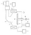
図1は、本発明における半導体処理装置の一例であるマイクロ波プラズマ装置を示す概略図である。この半導体処理装置は、マイクロ波を発振するマグネトロン1と、発振したマイクロ波をチャンバー3へと導入する導波管2と、クリーニングまたはエッチングを行うチャンバー3と、原料ガス及びクリーニングガス・エッチングガスを供給するガス供給装置7と、ガスを排気する真空排気装置9と、磁界を発生させるためチャンバー3の外側に設けられたソレノイドコイル6とから概略構成されている。この半導体処理装置では、クリーニングとエッチングの両方が行えるようになっている。 FIG. 1 is a schematic view showing a microwave plasma apparatus which is an example of a semiconductor processing apparatus according to the present invention. This semiconductor processing apparatus includes a magnetron 1 that oscillates a microwave, a
チャンバー3内には、高誘電率酸化物を成膜する下地となるシリコン基板8を載置する載置電極4が収容されている。この載置電極4には、シリコン基板8にバイアス電圧を印加するための高周波電源10が接続されている。また、ソレノイドコイル6には、直流電流を供給するための磁界発生用直流電源5が接続されている。 The chamber 3 accommodates a mounting electrode 4 on which a
マグネトロン1から発振した2.45GHzのマイクロ波は、導波管2を伝播しチャンバー3内に導かれる。チャンバー3の外側に設けられたソレノイドコイル6に、磁界発生用直流電源5から直流電流が供給されると、チャンバー3内に発生した875Gの磁界とマイクロ波電界によって、ガス供給装置7から供給したクリーニングガスまたはエッチングガスがプラズマ化される。このプラズマ化したガスにより、チャンバー3内に生成した高誘電率酸化物からなる堆積物・付着物のクリーニング、あるいはシリコン基板8上に成膜した高誘電率酸化物のエッチングを行うことができる。 The 2.45 GHz microwave oscillated from the magnetron 1 propagates through the
具体的には、チャンバー3内を真空排気し、酸素原子供与性ガスまたは酸化性ガスと、ハロゲン系ガスとを混合させたガスを導入する。チャンバー3内の真空度は、0.5〜2Pa(3.8〜15mTorr)であるのが好ましい。また、混合ガスの流量は、10〜50sccmであるのが好ましい。次いで、600W、240mAのマイクロ波電力をマグネトロン1に印加してマイクロ波を発振し、プラズマを発生させる。クリーニングの場合、載置電極4には、高周波電源10から電力を供給しない。また、この時、載置電極4とチャンバー3の内壁温度は室温〜350℃にするのが好ましい。 Specifically, the inside of the chamber 3 is evacuated and a gas in which an oxygen atom donating gas or oxidizing gas and a halogen-based gas are mixed is introduced. The degree of vacuum in the chamber 3 is preferably 0.5 to 2 Pa (3.8 to 15 mTorr). The flow rate of the mixed gas is preferably 10 to 50 sccm. Next, a microwave power of 600 W and 240 mA is applied to the magnetron 1 to oscillate the microwave and generate plasma. In the case of cleaning, power is not supplied to the mounting electrode 4 from the high
本発明のクリーニング方法によれば、酸素原子供与性ガスまたは酸化性ガスをハロゲン系ガスに混合して使用することにより、半導体処理装置のチャンバー内に生成した高誘電率酸化物からなる堆積物・付着物を高速で除去することができ、かつ他の化合物による堆積物の生成を防止することができる。また、クリーニングの速度が向上することにより、クリーニング時間が短縮でき、生産効率を向上させることができる。 According to the cleaning method of the present invention, a deposit made of a high dielectric constant oxide generated in a chamber of a semiconductor processing apparatus by using an oxygen atom donating gas or an oxidizing gas mixed with a halogen-based gas. -The deposits can be removed at high speed, and the formation of deposits by other compounds can be prevented. Further, since the cleaning speed is improved, the cleaning time can be shortened and the production efficiency can be improved.
また、一例として、化学気相堆積(CVD)法の成膜法に用いられる装置、原子層堆積(ALD)法の成膜法に用いられる装置について記載したが、これ以外にも高誘電率酸化物をエッチングするエッチング装置内に堆積・蓄積した高誘電率酸化物を上記と同様のクリーニング方法により高速で除去することができる。 As an example, an apparatus used for a chemical vapor deposition (CVD) film formation method and an apparatus used for an atomic layer deposition (ALD) film formation method have been described. High dielectric constant oxide deposited and accumulated in an etching apparatus for etching an object can be removed at high speed by the same cleaning method as described above.
[エッチング方法]
本発明に係るシリコン基板のエッチング方法とは、酸素原子供与性ガスまたは酸化性ガスのいずれかと、ハロゲン系ガスとを混合させたガスを、プラズマ処理または加熱処理により活性化し、シリコン基板上に成膜した高誘電率酸化物をエッチングするものである。[Etching method]
The method for etching a silicon substrate according to the present invention is a method in which a gas obtained by mixing either an oxygen atom donating gas or an oxidizing gas and a halogen-based gas is activated by plasma treatment or heat treatment, and is applied to the silicon substrate. The formed high dielectric constant oxide is etched.
高誘電率酸化物、混合ガス、プラズマ処理、加熱処理、これらを行う半導体処理装置については、上記クリーニング方法と同様であるので、その説明は省略する。クリーニング方法と異なるのは、エッチングの対象となるのがシリコン基板上に成膜した高誘電率酸化物である点である。 The high dielectric constant oxide, the mixed gas, the plasma treatment, the heat treatment, and the semiconductor processing apparatus for performing these are the same as in the cleaning method described above, and thus the description thereof is omitted. What is different from the cleaning method is that the high dielectric constant oxide film formed on the silicon substrate is the object of etching.
また、一般的に、エッチングを行う場合には、基板を載せた載置電極にバイアス電圧を印加して、プラズマ等により発生したイオンを加速して方向性を持たせて、これを基板上にたたきつける。この点が、クリーニングとは異なる。しかしながら、本発明に係るエッチング方法にあっては、バイアス電圧を印加する必要がない。ハロゲン系ガスに酸化性の性質を有する酸素原子供与性ガスまたは酸化性ガスを混合して用いることにより、バイアス電圧を印加することなく、高誘電率酸化物のエッチングを高速で行うことができる。 In general, when etching is performed, a bias voltage is applied to a mounting electrode on which a substrate is placed, and ions generated by plasma or the like are accelerated to give directionality, and this is applied to the substrate. Knock on. This is different from cleaning. However, in the etching method according to the present invention, it is not necessary to apply a bias voltage. By using a halogen-based gas mixed with an oxygen-atom donating gas or an oxidizing gas having an oxidizing property, etching of a high dielectric constant oxide can be performed at high speed without applying a bias voltage. .
具体的なエッチングの方法も、上記クリーニング方法と同様に行うことができる。この際、シリコン基板を250〜300℃に加熱することにより、エッチング速度をより向上させることができる。 A specific etching method can also be performed in the same manner as the above cleaning method. Under the present circumstances, an etching rate can be improved more by heating a silicon substrate to 250-300 degreeC.
また、本発明に係るエッチング方法では、高誘電率酸化物のみが選択的にエッチングされ、シリコン基板はエッチングされない。そのため、高誘電率酸化物とシリコン基板との選択比が1を超える高い値となり、下地のシリコン基板に一切ダメージを与えないエッチングを行うことができる。 In the etching method according to the present invention, only the high dielectric constant oxide is selectively etched, and the silicon substrate is not etched. Therefore, the selectivity between the high dielectric constant oxide and the silicon substrate is a high value exceeding 1, and etching can be performed without damaging the underlying silicon substrate.
以下、実施例により、本発明をさらに詳しく説明する。本発明は、下記実施例に何ら制限されるものではない。 Hereinafter, the present invention will be described in more detail by way of examples. The present invention is not limited to the following examples.
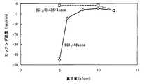
[実験例1]
図1に示した半導体処理装置を用いて、シリコン基板上に成膜した厚さ100nmのHfO2膜のエッチングを行った。プラズマを発生させるには、2.45GHzのマイクロ波と875Gの磁界を用いた。載置電極には、高周波電源から電力を供給せずに、シリコン基板をプラズマに暴露した。エッチングガスにはBCl3とO2との混合ガスを用い、O2の添加量を、0%、10%、20%と変化させた。エッチングの条件を表1に示す。プラズマ暴露前後のHfO2膜の膜厚の差を段差計で測定し、エッチング速度を求めた。混合ガス中の酸素添加量を変化させた時のHfO2膜のエッチング速度との関係を図2のグラフに示す。[Experimental Example 1]
Using the semiconductor processing apparatus shown in FIG. 1, an HfO2 film having a thickness of 100 nm formed on a silicon substrate was etched. In order to generate plasma, a microwave of 2.45 GHz and a magnetic field of 875 G were used. The mounting substrate was exposed to plasma without supplying power from a high frequency power source. A mixed gas of BCl3 and O2 was used as an etching gas, and the amount of O2 added was changed to 0%, 10%, and 20%. Table 1 shows the etching conditions. The difference in film thickness of the HfO2 film before and after plasma exposure was measured with a step gauge to determine the etching rate. FIG. 2 is a graph showing the relationship with the etching rate of the HfO2 film when the oxygen addition amount in the mixed gas is changed.

図2のグラフの結果から、酸素添加量が0%であるBCl3ガス単体を流した場合には、エッチングは起らず、エッチングガスに起因すると見られる堆積が観察された。しかし、酸素添加量が10%、20%の場合には、堆積物は生じず、良好なエッチング速度でエッチングされていることがわかった。From the result of the graph of FIG. 2, when a BCl3 gas alone having an oxygen addition amount of 0% was flowed, etching did not occur, and deposition that was attributed to the etching gas was observed. However, when the oxygen addition amount was 10% or 20%, no deposit was formed, and it was found that etching was performed at a good etching rate.
[実験例2]
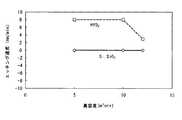
混合ガス中の酸素添加量を0%または10%とし、チャンバー内の真空度を5、6、8、10、12mTorrと変化させた以外は、実験例1と同様にしてエッチングを行い、HfO2膜の膜厚の差を測定し、エッチング速度を求めた。エッチングの条件を表2に示す。混合ガス中の酸素添加量及び真空度を変化させた時のHfO2膜のエッチング速度との関係を図3のグラフに示す。[Experiment 2]
Etching was performed in the same manner as in Experimental Example 1 except that the oxygen addition amount in the mixed gas was changed to 0% or 10% and the degree of vacuum in the chamber was changed to 5, 6, 8, 10, 12 mTorr, and HfO2 The difference in film thickness was measured to determine the etching rate. Table 2 shows the etching conditions. The graph of FIG. 3 shows the relationship between the oxygen addition amount in the mixed gas and the etching rate of the HfO2 film when the degree of vacuum is changed.
図3のグラフの結果から、酸素添加量が0%であるBCl3ガス単体を流した場合(実線)には、真空度が5mTorr及び6mTorrでは堆積が見られた。そして真空度が8mTorr以上になるとエッチングが観察された。しかし、酸素添加量が10%の場合(点線)では、堆積は一切観察されず、10mTorr以下の真空度では、BCl3ガス単体を流した場合よりもエッチング速度は大きいことがわかった。From the results of the graph of FIG. 3, when a single BCl3 gas with an oxygen addition amount of 0% was flowed (solid line), deposition was observed at a vacuum degree of 5 mTorr and 6 mTorr. Etching was observed when the degree of vacuum was 8 mTorr or more. However, no deposition was observed when the oxygen addition amount was 10% (dotted line), and it was found that the etching rate was higher at a vacuum level of 10 mTorr or less than when BCl3 gas alone was flowed.
[実験例3]
混合ガス中の酸素添加量を10%とし、チャンバー内の真空度を5、10、12mTorrに変化させた以外は、実験例2と同様にしてエッチングを行い、HfO2膜とシリコン基板の膜厚の差を測定し、エッチング速度を求めた。混合ガス中の真空度を変化させた時のHfO2膜及びシリコン基板のエッチング速度との関係を図4のグラフに示す。[Experiment 3]
Etching was performed in the same manner as in Experimental Example 2 except that the oxygen addition amount in the mixed gas was changed to 10% and the degree of vacuum in the chamber was changed to 5, 10, 12 mTorr, and the film thicknesses of the HfO2 film and the silicon substrate were changed. Was measured to determine the etching rate. The relationship between the etching rate of the HfO2 film and the silicon substrate when the degree of vacuum in the mixed gas is changed is shown in the graph of FIG.
図4のグラフの結果から、シリコン基板のエッチングは観察されず、また堆積もなかった。HfO2膜については、良好なエッチング速度でエッチングされ、堆積は見られなかった。この場合の選択比は1を越える値であった。From the results of the graph of FIG. 4, no etching of the silicon substrate was observed and no deposition was observed. The HfO2 film was etched at a good etching rate, and no deposition was observed. In this case, the selection ratio was a value exceeding 1.
以上の結果から、本発明のエッチング方法によれば、酸素原子供与性ガスまたは酸化性ガスをハロゲン系ガスに混合して使用することにより、バイアス電圧を印加することなく、シリコン基板上に成膜した高誘電率酸化物を、選択比が1を超える高い選択性をもってエッチングできることが確認された。 From the above results, according to the etching method of the present invention, the oxygen atom donating gas or oxidizing gas is mixed with the halogen-based gas and used on the silicon substrate without applying a bias voltage. It was confirmed that the filmed high dielectric constant oxide can be etched with high selectivity exceeding 1 in selectivity.
3 チャンバー
8 シリコン基板
Claims (4)
Translated fromJapanese酸素と、BCl3とを混合させた混合ガスを、載置電極にバイアス電圧を印加しないプラズマ処理または加熱処理により活性化し、前記堆積物または付着物を除去することを特徴とする半導体処理装置のクリーニング方法。A method for cleaning a semiconductor processing apparatus for removing deposits or deposits made of a high dielectric constant oxide generated in a chamber of a semiconductor processing apparatus,
A semiconductor processing apparatus characterized in that amixed gas in whichoxygen andBCl3 are mixed is activated by a plasma treatment or a heat treatmentwithout applying a bias voltage to amounting electrode, and the deposits or deposits are removed. Cleaning method.
酸素と、BCl3とを混合させた混合ガスを、載置電極にバイアス電圧を印加しないプラズマ処理または加熱処理により活性化し、前記高誘電率酸化物をエッチングすることを特徴とするシリコン基板のエッチング方法。A method of etching a high dielectric constant oxide film formed on a silicon substrate,
Etching the high dielectric constant oxide by activating amixed gas in whichoxygen andBCl3 are mixed by plasma treatment or heat treatmentwithout applying a bias voltage to the mounting electrode, and etching the silicon substrate Method.
Priority Applications (6)
| Application Number | Priority Date | Filing Date | Title |
|---|---|---|---|
| JP2004374107AJP4836112B2 (en) | 2004-12-24 | 2004-12-24 | Semiconductor processing apparatus cleaning method and silicon substrate etching method |
| PCT/JP2005/023625WO2006068235A1 (en) | 2004-12-24 | 2005-12-22 | Method for cleaning of semiconductor processing apparatus and method for ethching silicon substrate |
| TW094145821ATWI381438B (en) | 2004-12-24 | 2005-12-22 | Process for cleaning semiconductor treating apparatus and process for etching silicon substrate |
| US11/793,423US20080160777A1 (en) | 2004-12-24 | 2005-12-22 | Cleaning Method For Processing Chamber Of Semiconductor Substrates And Etching Method For Silicon Substrates Technical Field |
| KR1020077015290AKR100876215B1 (en) | 2004-12-24 | 2005-12-22 | Cleaning method of semiconductor processing device and etching method of silicon substrate |
| EP05819632AEP1840946A1 (en) | 2004-12-24 | 2005-12-22 | Method for cleaning of semiconductor processing apparatus and method for ethching silicon substrate |
Applications Claiming Priority (1)
| Application Number | Priority Date | Filing Date | Title |
|---|---|---|---|
| JP2004374107AJP4836112B2 (en) | 2004-12-24 | 2004-12-24 | Semiconductor processing apparatus cleaning method and silicon substrate etching method |
Publications (2)
| Publication Number | Publication Date |
|---|---|
| JP2006179834A JP2006179834A (en) | 2006-07-06 |
| JP4836112B2true JP4836112B2 (en) | 2011-12-14 |
Family
ID=36601832
Family Applications (1)
| Application Number | Title | Priority Date | Filing Date |
|---|---|---|---|
| JP2004374107AExpired - Fee RelatedJP4836112B2 (en) | 2004-12-24 | 2004-12-24 | Semiconductor processing apparatus cleaning method and silicon substrate etching method |
Country Status (6)
| Country | Link |
|---|---|
| US (1) | US20080160777A1 (en) |
| EP (1) | EP1840946A1 (en) |
| JP (1) | JP4836112B2 (en) |
| KR (1) | KR100876215B1 (en) |
| TW (1) | TWI381438B (en) |
| WO (1) | WO2006068235A1 (en) |
Families Citing this family (28)
| Publication number | Priority date | Publication date | Assignee | Title |
|---|---|---|---|---|
| JP2008060171A (en)* | 2006-08-29 | 2008-03-13 | Taiyo Nippon Sanso Corp | Cleaning method for semiconductor processing apparatus |
| US8183161B2 (en)* | 2006-09-12 | 2012-05-22 | Tokyo Electron Limited | Method and system for dry etching a hafnium containing material |
| US20080271753A1 (en)* | 2007-05-03 | 2008-11-06 | L'air Liquide Societe Anonyme Pour I'etude Et I'exploitation Des Procedes Georges Claude | Method of cleaninig stannane distribution system |
| JP2008288281A (en)* | 2007-05-15 | 2008-11-27 | Hitachi Kokusai Electric Inc | Semiconductor device manufacturing method and substrate processing apparatus |
| JP2009021584A (en)* | 2007-06-27 | 2009-01-29 | Applied Materials Inc | High temperature material gate structure high temperature etching method |
| JP5110987B2 (en)* | 2007-07-05 | 2012-12-26 | 株式会社日立ハイテクノロジーズ | Plasma processing method and computer-readable recording medium |
| JP5297615B2 (en)* | 2007-09-07 | 2013-09-25 | 株式会社日立ハイテクノロジーズ | Dry etching method |
| US20100186774A1 (en)* | 2007-09-19 | 2010-07-29 | Hironobu Miya | Cleaning method and substrate processing apparatus |
| JP2009123795A (en)* | 2007-11-13 | 2009-06-04 | Hitachi Kokusai Electric Inc | Semiconductor device manufacturing method and substrate processing apparatus |
| JP4994197B2 (en)* | 2007-11-16 | 2012-08-08 | 株式会社日立国際電気 | Semiconductor device manufacturing method and substrate processing apparatus |
| JP5011148B2 (en)* | 2008-02-06 | 2012-08-29 | 大陽日酸株式会社 | Semiconductor device manufacturing method, cleaning method, and substrate processing apparatus |
| JP2009188257A (en)* | 2008-02-07 | 2009-08-20 | Tokyo Electron Ltd | Plasma etching method, plasma etching apparatus, and storage medium |
| KR20100006009A (en)* | 2008-07-08 | 2010-01-18 | 주성엔지니어링(주) | Apparatus for manufacturing semiconductor |
| KR101422155B1 (en) | 2010-02-01 | 2014-07-22 | 샌트랄 글래스 컴퍼니 리미티드 | Dry etching agent and dry etching method using the same |
| US8784676B2 (en)* | 2012-02-03 | 2014-07-22 | Lam Research Corporation | Waferless auto conditioning |
| US9441290B2 (en)* | 2013-05-29 | 2016-09-13 | Varian Semiconductor Equipment Associates, Inc. | System and method of improving implant quality in a plasma-based implant system |
| JP6422262B2 (en) | 2013-10-24 | 2018-11-14 | 東京エレクトロン株式会社 | Plasma processing method and plasma processing apparatus |
| CN104841662B (en)* | 2014-02-19 | 2017-04-05 | 宇宙电路板设备(深圳)有限公司 | A kind of wet process equipment cleaning method and device |
| KR102410571B1 (en) | 2016-12-09 | 2022-06-22 | 에이에스엠 아이피 홀딩 비.브이. | Thermal Atomic Layer Etching Processes |
| US10283319B2 (en)* | 2016-12-22 | 2019-05-07 | Asm Ip Holding B.V. | Atomic layer etching processes |
| US12076763B2 (en)* | 2017-06-05 | 2024-09-03 | Applied Materials, Inc. | Selective in-situ cleaning of high-k films from processing chamber using reactive gas precursor |
| US20180350571A1 (en)* | 2017-06-05 | 2018-12-06 | Applied Materials, Inc. | Selective in-situ cleaning of high-k films from processing chamber using reactive gas precursor |
| US20180347037A1 (en)* | 2017-06-05 | 2018-12-06 | Applied Materials, Inc. | Selective in-situ cleaning of high-k films from processing chamber using reactive gas precursor |
| KR20200039827A (en)* | 2017-09-11 | 2020-04-16 | 어플라이드 머티어리얼스, 인코포레이티드 | Selective in-situ cleaning of high-K films from processing chamber using reactive gas precursor |
| CN111014336B (en)* | 2018-10-10 | 2025-07-25 | 江苏昆仑光源材料有限公司 | Wire unwinding system for producing high-purity nano-scale cuprous oxide wrapping layer Dumet wire |
| KR20220082871A (en) | 2020-01-30 | 2022-06-17 | 쇼와 덴코 가부시키가이샤 | Etching method |
| US11572622B2 (en) | 2020-09-14 | 2023-02-07 | Applied Materials, Inc. | Systems and methods for cleaning low-k deposition chambers |
| CN115083877B (en)* | 2021-03-11 | 2024-08-23 | 中国科学院微电子研究所 | Method for improving dry etching rate stability of polycrystalline silicon film and etching chamber |
Family Cites Families (7)
| Publication number | Priority date | Publication date | Assignee | Title |
|---|---|---|---|---|
| JP3367600B2 (en)* | 1998-06-08 | 2003-01-14 | シャープ株式会社 | Method of manufacturing dielectric thin film element |
| JP4222707B2 (en)* | 2000-03-24 | 2009-02-12 | 東京エレクトロン株式会社 | Plasma processing apparatus and method, gas supply ring and dielectric |
| JP2002057149A (en)* | 2000-08-08 | 2002-02-22 | Tokyo Electron Ltd | Treatment device and its cleaning method |
| CA2435852A1 (en)* | 2000-11-14 | 2002-05-23 | Sekisui Chemical Co., Ltd. | A method for plasma treatment under the atmospheric pressure and an equipment therefor |
| US20040014327A1 (en)* | 2002-07-18 | 2004-01-22 | Bing Ji | Method for etching high dielectric constant materials and for cleaning deposition chambers for high dielectric constant materials |
| US7357138B2 (en)* | 2002-07-18 | 2008-04-15 | Air Products And Chemicals, Inc. | Method for etching high dielectric constant materials and for cleaning deposition chambers for high dielectric constant materials |
| JP4283017B2 (en)* | 2003-03-25 | 2009-06-24 | 富士通マイクロエレクトロニクス株式会社 | Manufacturing method of semiconductor device |
- 2004
- 2004-12-24JPJP2004374107Apatent/JP4836112B2/ennot_activeExpired - Fee Related
- 2005
- 2005-12-22KRKR1020077015290Apatent/KR100876215B1/ennot_activeExpired - Fee Related
- 2005-12-22TWTW094145821Apatent/TWI381438B/ennot_activeIP Right Cessation
- 2005-12-22USUS11/793,423patent/US20080160777A1/ennot_activeAbandoned
- 2005-12-22EPEP05819632Apatent/EP1840946A1/ennot_activeWithdrawn
- 2005-12-22WOPCT/JP2005/023625patent/WO2006068235A1/ennot_activeCeased
Also Published As
| Publication number | Publication date |
|---|---|
| JP2006179834A (en) | 2006-07-06 |
| EP1840946A1 (en) | 2007-10-03 |
| US20080160777A1 (en) | 2008-07-03 |
| TWI381438B (en) | 2013-01-01 |
| KR100876215B1 (en) | 2008-12-31 |
| TW200625442A (en) | 2006-07-16 |
| WO2006068235A1 (en) | 2006-06-29 |
| KR20070086917A (en) | 2007-08-27 |
Similar Documents
| Publication | Publication Date | Title |
|---|---|---|
| JP4836112B2 (en) | Semiconductor processing apparatus cleaning method and silicon substrate etching method | |
| KR102483741B1 (en) | Apparatus and methods for spacer deposition and selective removal in advanced patterning processes | |
| CN108573866B (en) | Oxide film removing method and apparatus, and contact forming method and system | |
| KR101106882B1 (en) | How to Etch High-Material Material Gate Structures at High Temperature | |
| JP2004146787A (en) | Method for etching high dielectric constant material, and for cleaning deposition chamber for high dielectric constant material | |
| US9960049B2 (en) | Two-step fluorine radical etch of hafnium oxide | |
| JP2009033202A (en) | Method of removing high dielectric constant material from deposition chamber | |
| CN109219866B (en) | etching method | |
| JP2008060171A (en) | Cleaning method for semiconductor processing apparatus | |
| JP4147017B2 (en) | Microwave plasma substrate processing equipment | |
| TW202249117A (en) | Atomic layer etching of metal oxides | |
| US20040129674A1 (en) | Method and system to enhance the removal of high-k dielectric materials | |
| JP5297615B2 (en) | Dry etching method | |
| TW202242953A (en) | Tin oxide and tin carbide materials for semiconductor patterning applications | |
| WO2023234214A1 (en) | Etching method and plasma processing device | |
| Nakamura et al. | Plasma etching of high-k and metal gate materials | |
| JP2006339523A (en) | Cleaning method for semiconductor processing apparatus and etching method for high dielectric constant oxide film | |
| CN101339903A (en) | Method for high temperature etching of high-K material gate structures | |
| CN112420508B (en) | Etching method and substrate processing device | |
| JP5642427B2 (en) | Plasma processing method | |
| CN119256389A (en) | Etching method and plasma processing apparatus | |
| JP2008515220A (en) | Method and system for forming features in a High-k layer | |
| JPH053178A (en) | Method for manufacturing semiconductor device | |
| KR100851454B1 (en) | New methodologies to reduce process sensitivity to the chamber condition | |
| CN115020220B (en) | Silicon oxide film surface fluorine element treatment method and etching method |
Legal Events
| Date | Code | Title | Description |
|---|---|---|---|
| A621 | Written request for application examination | Free format text:JAPANESE INTERMEDIATE CODE: A621 Effective date:20071030 | |
| A131 | Notification of reasons for refusal | Free format text:JAPANESE INTERMEDIATE CODE: A131 Effective date:20100727 | |
| A521 | Request for written amendment filed | Free format text:JAPANESE INTERMEDIATE CODE: A523 Effective date:20100913 | |
| TRDD | Decision of grant or rejection written | ||
| A01 | Written decision to grant a patent or to grant a registration (utility model) | Free format text:JAPANESE INTERMEDIATE CODE: A01 Effective date:20110823 | |
| A01 | Written decision to grant a patent or to grant a registration (utility model) | Free format text:JAPANESE INTERMEDIATE CODE: A01 | |
| A61 | First payment of annual fees (during grant procedure) | Free format text:JAPANESE INTERMEDIATE CODE: A61 Effective date:20110921 | |
| FPAY | Renewal fee payment (event date is renewal date of database) | Free format text:PAYMENT UNTIL: 20141007 Year of fee payment:3 | |
| R150 | Certificate of patent or registration of utility model | Ref document number:4836112 Country of ref document:JP Free format text:JAPANESE INTERMEDIATE CODE: R150 Free format text:JAPANESE INTERMEDIATE CODE: R150 | |
| R250 | Receipt of annual fees | Free format text:JAPANESE INTERMEDIATE CODE: R250 | |
| R250 | Receipt of annual fees | Free format text:JAPANESE INTERMEDIATE CODE: R250 | |
| R250 | Receipt of annual fees | Free format text:JAPANESE INTERMEDIATE CODE: R250 | |
| R250 | Receipt of annual fees | Free format text:JAPANESE INTERMEDIATE CODE: R250 | |
| R250 | Receipt of annual fees | Free format text:JAPANESE INTERMEDIATE CODE: R250 | |
| R250 | Receipt of annual fees | Free format text:JAPANESE INTERMEDIATE CODE: R250 | |
| R250 | Receipt of annual fees | Free format text:JAPANESE INTERMEDIATE CODE: R250 | |
| S111 | Request for change of ownership or part of ownership | Free format text:JAPANESE INTERMEDIATE CODE: R313115 | |
| R350 | Written notification of registration of transfer | Free format text:JAPANESE INTERMEDIATE CODE: R350 | |
| R250 | Receipt of annual fees | Free format text:JAPANESE INTERMEDIATE CODE: R250 | |
| R250 | Receipt of annual fees | Free format text:JAPANESE INTERMEDIATE CODE: R250 | |
| LAPS | Cancellation because of no payment of annual fees |