JP4834369B2 - Semiconductor device - Google Patents
Semiconductor deviceDownload PDFInfo
- Publication number
- JP4834369B2 JP4834369B2JP2005294710AJP2005294710AJP4834369B2JP 4834369 B2JP4834369 B2JP 4834369B2JP 2005294710 AJP2005294710 AJP 2005294710AJP 2005294710 AJP2005294710 AJP 2005294710AJP 4834369 B2JP4834369 B2JP 4834369B2
- Authority
- JP
- Japan
- Prior art keywords
- semiconductor chip
- semiconductor
- semiconductor device
- wiring
- region
- Prior art date
- Legal status (The legal status is an assumption and is not a legal conclusion. Google has not performed a legal analysis and makes no representation as to the accuracy of the status listed.)
- Expired - Fee Related
Links
Images


Classifications
- H—ELECTRICITY
- H01—ELECTRIC ELEMENTS
- H01L—SEMICONDUCTOR DEVICES NOT COVERED BY CLASS H10
- H01L25/00—Assemblies consisting of a plurality of semiconductor or other solid state devices
- H01L25/18—Assemblies consisting of a plurality of semiconductor or other solid state devices the devices being of the types provided for in two or more different main groups of the same subclass of H10B, H10D, H10F, H10H, H10K or H10N
- H—ELECTRICITY
- H01—ELECTRIC ELEMENTS
- H01L—SEMICONDUCTOR DEVICES NOT COVERED BY CLASS H10
- H01L23/00—Details of semiconductor or other solid state devices
- H01L23/28—Encapsulations, e.g. encapsulating layers, coatings, e.g. for protection
- H01L23/31—Encapsulations, e.g. encapsulating layers, coatings, e.g. for protection characterised by the arrangement or shape
- H01L23/3107—Encapsulations, e.g. encapsulating layers, coatings, e.g. for protection characterised by the arrangement or shape the device being completely enclosed
- H01L23/3114—Encapsulations, e.g. encapsulating layers, coatings, e.g. for protection characterised by the arrangement or shape the device being completely enclosed the device being a chip scale package, e.g. CSP
- H—ELECTRICITY
- H01—ELECTRIC ELEMENTS
- H01L—SEMICONDUCTOR DEVICES NOT COVERED BY CLASS H10
- H01L25/00—Assemblies consisting of a plurality of semiconductor or other solid state devices
- H01L25/03—Assemblies consisting of a plurality of semiconductor or other solid state devices all the devices being of a type provided for in a single subclass of subclasses H10B, H10D, H10F, H10H, H10K or H10N, e.g. assemblies of rectifier diodes
- H01L25/04—Assemblies consisting of a plurality of semiconductor or other solid state devices all the devices being of a type provided for in a single subclass of subclasses H10B, H10D, H10F, H10H, H10K or H10N, e.g. assemblies of rectifier diodes the devices not having separate containers
- H01L25/065—Assemblies consisting of a plurality of semiconductor or other solid state devices all the devices being of a type provided for in a single subclass of subclasses H10B, H10D, H10F, H10H, H10K or H10N, e.g. assemblies of rectifier diodes the devices not having separate containers the devices being of a type provided for in group H10D89/00
- H01L25/0657—Stacked arrangements of devices
- H—ELECTRICITY
- H01—ELECTRIC ELEMENTS
- H01L—SEMICONDUCTOR DEVICES NOT COVERED BY CLASS H10
- H01L2224/00—Indexing scheme for arrangements for connecting or disconnecting semiconductor or solid-state bodies and methods related thereto as covered by H01L24/00
- H01L2224/01—Means for bonding being attached to, or being formed on, the surface to be connected, e.g. chip-to-package, die-attach, "first-level" interconnects; Manufacturing methods related thereto
- H01L2224/42—Wire connectors; Manufacturing methods related thereto
- H01L2224/47—Structure, shape, material or disposition of the wire connectors after the connecting process
- H01L2224/48—Structure, shape, material or disposition of the wire connectors after the connecting process of an individual wire connector
- H01L2224/4805—Shape
- H01L2224/4809—Loop shape
- H01L2224/48091—Arched
- H—ELECTRICITY
- H01—ELECTRIC ELEMENTS
- H01L—SEMICONDUCTOR DEVICES NOT COVERED BY CLASS H10
- H01L2224/00—Indexing scheme for arrangements for connecting or disconnecting semiconductor or solid-state bodies and methods related thereto as covered by H01L24/00
- H01L2224/01—Means for bonding being attached to, or being formed on, the surface to be connected, e.g. chip-to-package, die-attach, "first-level" interconnects; Manufacturing methods related thereto
- H01L2224/42—Wire connectors; Manufacturing methods related thereto
- H01L2224/47—Structure, shape, material or disposition of the wire connectors after the connecting process
- H01L2224/48—Structure, shape, material or disposition of the wire connectors after the connecting process of an individual wire connector
- H01L2224/481—Disposition
- H01L2224/48151—Connecting between a semiconductor or solid-state body and an item not being a semiconductor or solid-state body, e.g. chip-to-substrate, chip-to-passive
- H01L2224/48221—Connecting between a semiconductor or solid-state body and an item not being a semiconductor or solid-state body, e.g. chip-to-substrate, chip-to-passive the body and the item being stacked
- H01L2224/48225—Connecting between a semiconductor or solid-state body and an item not being a semiconductor or solid-state body, e.g. chip-to-substrate, chip-to-passive the body and the item being stacked the item being non-metallic, e.g. insulating substrate with or without metallisation
- H01L2224/48227—Connecting between a semiconductor or solid-state body and an item not being a semiconductor or solid-state body, e.g. chip-to-substrate, chip-to-passive the body and the item being stacked the item being non-metallic, e.g. insulating substrate with or without metallisation connecting the wire to a bond pad of the item
- H—ELECTRICITY
- H01—ELECTRIC ELEMENTS
- H01L—SEMICONDUCTOR DEVICES NOT COVERED BY CLASS H10
- H01L2225/00—Details relating to assemblies covered by the group H01L25/00 but not provided for in its subgroups
- H01L2225/03—All the devices being of a type provided for in the same main group of the same subclass of class H10, e.g. assemblies of rectifier diodes
- H01L2225/04—All the devices being of a type provided for in the same main group of the same subclass of class H10, e.g. assemblies of rectifier diodes the devices not having separate containers
- H01L2225/065—All the devices being of a type provided for in the same main group of the same subclass of class H10
- H01L2225/06503—Stacked arrangements of devices
- H01L2225/06513—Bump or bump-like direct electrical connections between devices, e.g. flip-chip connection, solder bumps
- H—ELECTRICITY
- H01—ELECTRIC ELEMENTS
- H01L—SEMICONDUCTOR DEVICES NOT COVERED BY CLASS H10
- H01L24/00—Arrangements for connecting or disconnecting semiconductor or solid-state bodies; Methods or apparatus related thereto
- H01L24/01—Means for bonding being attached to, or being formed on, the surface to be connected, e.g. chip-to-package, die-attach, "first-level" interconnects; Manufacturing methods related thereto
- H01L24/42—Wire connectors; Manufacturing methods related thereto
- H01L24/47—Structure, shape, material or disposition of the wire connectors after the connecting process
- H01L24/48—Structure, shape, material or disposition of the wire connectors after the connecting process of an individual wire connector
- H—ELECTRICITY
- H01—ELECTRIC ELEMENTS
- H01L—SEMICONDUCTOR DEVICES NOT COVERED BY CLASS H10
- H01L2924/00—Indexing scheme for arrangements or methods for connecting or disconnecting semiconductor or solid-state bodies as covered by H01L24/00
- H01L2924/0001—Technical content checked by a classifier
- H01L2924/00014—Technical content checked by a classifier the subject-matter covered by the group, the symbol of which is combined with the symbol of this group, being disclosed without further technical details
- H—ELECTRICITY
- H01—ELECTRIC ELEMENTS
- H01L—SEMICONDUCTOR DEVICES NOT COVERED BY CLASS H10
- H01L2924/00—Indexing scheme for arrangements or methods for connecting or disconnecting semiconductor or solid-state bodies as covered by H01L24/00
- H01L2924/10—Details of semiconductor or other solid state devices to be connected
- H01L2924/11—Device type
- H01L2924/12—Passive devices, e.g. 2 terminal devices
- H01L2924/1204—Optical Diode
- H01L2924/12044—OLED
- H—ELECTRICITY
- H01—ELECTRIC ELEMENTS
- H01L—SEMICONDUCTOR DEVICES NOT COVERED BY CLASS H10
- H01L2924/00—Indexing scheme for arrangements or methods for connecting or disconnecting semiconductor or solid-state bodies as covered by H01L24/00
- H01L2924/15—Details of package parts other than the semiconductor or other solid state devices to be connected
- H01L2924/181—Encapsulation
Landscapes
- Engineering & Computer Science (AREA)
- Microelectronics & Electronic Packaging (AREA)
- Power Engineering (AREA)
- Physics & Mathematics (AREA)
- Condensed Matter Physics & Semiconductors (AREA)
- General Physics & Mathematics (AREA)
- Computer Hardware Design (AREA)
- Structures Or Materials For Encapsulating Or Coating Semiconductor Devices Or Solid State Devices (AREA)
Description
Translated fromJapanese本発明は、半導体装置に関する。 The present invention relates to a semiconductor device.
従来の半導体装置としては、例えば特許文献1または非特許文献1に記載されたものがある。特許文献1に記載の半導体装置においては、第1の半導体チップ上に第2の半導体チップがフリップチップ実装されている。これらの第1および第2の半導体チップ間には、アンダーフィル樹脂が充填されている。 Examples of conventional semiconductor devices include those described in
一方、非特許文献1に記載の半導体装置においては、第1の半導体チップ上に、シールリングを介して、第2の半導体チップが載置されている。第2の半導体チップは、第1の半導体チップに比べて面積が小さく、第1の半導体チップの一部領域上に設けられている。この第2の半導体チップの縁部に沿って、上記シールリングが設けられている。これにより、第1および第2の半導体チップの間の領域は、シールリングによって気密に封止されている。そして、この気密封止された領域において、両チップが接続端子によって互いに電気的に接続されている。
特許文献1の半導体装置では、第1および第2の半導体チップ間にアンダーフィル樹脂を充填することにより、両チップ間の接続信頼性を確保している。ところが、両チップを接続するバンプ等の導電部材どうしの間隔を狭くし過ぎると、両チップ間にアンダーフィル樹脂を充分に注入することが困難となる。それにより、上記導電部材を高密度に形成することが妨げられてしまう。換言すれば、両チップ間の接続密度の向上が妨げられてしまう。 In the semiconductor device of
これに対して、非特許文献1の半導体装置によれば、第1および第2の半導体チップ間の間隙をシールリングで気密封止することによって、当該間隙にアンダーフィル樹脂を充填することなく、両チップ間の接続信頼性を長期的に維持することが可能となる。したがって、第1および第2の半導体チップ間にシールリングを設けることは、両チップ間の接続密度を向上させる上で好ましい。 On the other hand, according to the semiconductor device of Non-Patent
しかしながら、その一方で、同文献の半導体装置においては、第2の半導体チップの信号を外部に取り出すための信号経路を、シールリングを迂回するように設けなければならない。したがって、第2の半導体チップの信号は、第1の半導体チップの内部配線を経由して外部に取り出されることとなる。そのため、信号経路の電気抵抗が増大し、半導体装置の電気特性の劣化につながってしまう。 However, on the other hand, in the semiconductor device disclosed in this document, a signal path for taking out the signal of the second semiconductor chip to the outside must be provided so as to bypass the seal ring. Therefore, the signal of the second semiconductor chip is extracted outside via the internal wiring of the first semiconductor chip. As a result, the electrical resistance of the signal path increases, leading to deterioration of the electrical characteristics of the semiconductor device.
本発明による半導体装置は、第1の半導体チップと、上記第1の半導体チップと所定の間隔を置いて、当該第1の半導体チップの一面上に設けられた第2の半導体チップと、上記第1および第2の半導体チップ間に介在するシールリングと、を備え、上記第1および第2の半導体チップ間には、上記シールリングの内側の領域である内部領域と、上記シールリングの外側の領域である外部領域とが設けられていることを特徴とする。上記内部領域には、上記第1および第2の半導体チップを電気的に接続する第1の導電部材が設けられており、上記外部領域には、上記第1および第2の半導体チップを電気的に接続する第2の導電部材が設けられている。また、内部領域は、不活性ガスで満たされた状態または真空状態にあってもよい。外部領域には絶縁性樹脂が充填されていてもよい。The semiconductor device according to the present invention includes a first semiconductor chip, a second semiconductor chip provided on one surface of the first semiconductor chip at a predetermined interval, and the first semiconductor chip. A seal ring interposed between the first semiconductor chip and the second semiconductor chip, and between the first semiconductor chip and the second semiconductor chip, an inner region that is an inner region of the seal ring and an outer region of the seal ring. An external region that is a region is provided.The internal region is provided with a first conductive member that electrically connects the first and second semiconductor chips, and the first and second semiconductor chips are electrically connected to the external region. A second conductive member connected to is provided. Further, the inner region may be in a state filled with an inert gas or in a vacuum state. The external region may be filled with an insulating resin.
この半導体装置においては、第1および第2の半導体チップ間に、シールリングに囲まれた領域(内部領域)と囲まれない領域(外部領域)とが設けられている。これにより、内部領域だけでなく外部領域においても、両チップを電気的に接続することが可能となる。したがって、この外部領域を利用することにより、一方のチップの信号を、他方のチップの内部配線を経由することなしに取り出すことができる。このため、信号経路の電気抵抗を小さく抑えることができる。 In this semiconductor device, a region (inner region) surrounded by a seal ring and a region (outer region) not surrounded are provided between the first and second semiconductor chips. As a result, both chips can be electrically connected not only in the internal region but also in the external region. Therefore, by using this external area, the signal of one chip can be taken out without going through the internal wiring of the other chip. For this reason, the electrical resistance of the signal path can be kept small.
本発明によれば、電気特性に優れた半導体装置が実現される。 According to the present invention, a semiconductor device having excellent electrical characteristics is realized.
以下、図面を参照しつつ、本発明による半導体装置の好適な実施形態について詳細に説明する。なお、図面の説明においては、同一要素には同一符号を付し、重複する説明を省略する。 Hereinafter, preferred embodiments of a semiconductor device according to the present invention will be described in detail with reference to the drawings. In the description of the drawings, the same reference numerals are assigned to the same elements, and duplicate descriptions are omitted.
(第1実施形態)
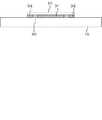
図1は、本発明による半導体装置の第1実施形態を示す断面図である。半導体装置1は、半導体チップ10(第1の半導体チップ)、半導体チップ20(第2の半導体チップ)、およびシールリング30を備えている。(First embodiment)
FIG. 1 is a sectional view showing a first embodiment of a semiconductor device according to the present invention. The
半導体チップ20は、半導体チップ10と所定の間隔を置いて、半導体チップ10の面S1上に設けられている。本実施形態において、半導体チップ10は半導体チップ20よりもチップ面積が大きい。半導体チップ10および半導体チップ20は、例えば、それぞれメモリチップおよびロジックLSIチップである。 The
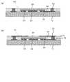
これらの半導体チップ10と半導体チップ20との間には、シールリング30が介在している。すなわち、半導体チップ20は、シールリング30を介して半導体チップ10上に載置されている。図2に示すように、半導体チップ10および半導体チップ20間には、シールリング30の内側の領域である内部領域D1と、シールリング30の外側の領域である外部領域D2とが設けられている。同図においては、半導体装置1の構成要素うち、半導体チップ10,20およびシールリング30のみを示し、その他の図示を省略している。 A
内部領域D1は、シールリング30で包囲されることにより、気密に封止されている。この内部領域D1は、窒素またはアルゴン等の不活性ガスで満たされた状態にあってもよく、真空状態にあってもよい。一方、外部領域D2は、シールリング30によって包囲されていない。この領域D2には、後述する絶縁性樹脂層50を構成する絶縁性樹脂が充填されている。 The inner region D1 is hermetically sealed by being surrounded by the
内部領域D1および外部領域D2のそれぞれには、導電部材32(第1の導電部材)および導電部材34(第2の導電部材)が形成されている。導電部材32,34は、半導体チップ10と半導体チップ20とを電気的に接続する電気的接続手段である。これらの導電部材32,34は、シールリング30と同一の導電材料によって構成されている。 In each of the internal region D1 and the external region D2, a conductive member 32 (first conductive member) and a conductive member 34 (second conductive member) are formed. The
図3は、半導体装置1を示す平面図である。同図においては、後述する絶縁性樹脂層50、配線層60、配線62および外部電極端子64の図示を省略する一方で、半導体チップ20の影に隠れた部分(半導体チップ10と半導体チップ20との間の間隙部分)を図示している。この図からわかるように、導電部材32の配列ピッチは、導電部材34のそれよりも小さい。導電部材32および導電部材34の配列ピッチは、例えば、それぞれ1μmおよび10μmである。また、平面視での面積についても、導電部材32の方が導電部材34よりも小さい。 FIG. 3 is a plan view showing the
図1に戻って、半導体チップ10の面S1上には、配線40が形成されている。配線40には、上述の導電部材34が接続されている。また、半導体チップ10の面S1上には、半導体チップ20を覆う絶縁性樹脂層50(絶縁層)が形成されている。この絶縁性樹脂層50中には、配線40に接続された導体ポスト42(導体プラグ)が埋め込まれている。 Returning to FIG. 1, the
絶縁性樹脂層50上には、配線層60を介して外部電極端子64が設けられている。外部電極端子64は、導体ポスト42と電気的に接続されている。具体的には、外部電極端子64は、配線層60中に形成された配線62に直接接続されており、この配線62が導体ポスト42に直接接続されている。これにより、外部電極端子64は、上述の導電部材34と電気的に接続された構成となっている。 An
図4および図5を参照しつつ、半導体装置1の製造方法の一例を説明する。まず、半導体チップ10,20を準備する。このとき、半導体チップ10はウエハ状態にあることが好ましい。そして、半導体チップ10上に、シールリング30a、電極32aおよび配線40を形成する。これらのシールリング30a、電極32aおよび配線40の材料としては、例えばCuを用いることができる。その後、配線40上に導体ポスト42を形成する。導体ポスト42は、例えば、配線40を給電層としためっき法により形成することができる。また、半導体チップ20上には、シールリング30b、電極32bおよび電極34bを形成する(図4(a))。 An example of a method for manufacturing the
これらのシールリング30b、電極32bおよび電極34bは、例えば、Cu膜およびSn膜の積層構造とすることができる。すなわち、これらは、半導体チップ20上に形成されたCu膜と、その上に形成されたSn膜とによって構成することができる。 The
続いて、半導体チップ10と半導体チップ20とを接合する。これにより、シールリング30aとシールリング30bとで構成されたシールリング30、電極32aと電極32bとで構成された導電部材32、および配線40の一部と電極34bとで構成された導電部材34が形成される(図4(b))。なお、この接合は、不活性ガス雰囲気中または真空中で行うことが好ましい。 Subsequently, the
次に、モールド法、印刷法またはスピンコート法等により、半導体チップ10上に絶縁性樹脂層50を形成する。これにより、上述の外部領域D2(図2参照)が絶縁性樹脂により封止される(図5(a))。この絶縁性樹脂層50の形成は、真空中で行うことが好ましい。なお、絶縁性樹脂層50を形成した後、導体ポスト42を絶縁性樹脂層50の表面に露出させるために、必要に応じて、絶縁性樹脂層50を研削してもよい。 Next, the insulating
続いて、配線62を含む配線層60を形成する(図5(b))。さらに、配線62に接続された外部電極端子64を形成する。以上の工程を半導体チップ10がウエハ状態のまま実行した場合には、その後、半導体チップ10をダイシング等の手段により個片化する。以上により、図1に示す半導体装置1を得る。 Subsequently, the
本実施形態の効果を説明する。半導体装置1においては、半導体チップ10と半導体チップ20と間に、シールリング30に囲まれた内部領域と囲まれない外部領域とが設けられている。これにより、内部領域だけでなく外部領域においても、両チップを電気的に接続することが可能となる。実際、半導体装置1においては、半導体チップ10,20が、外部領域に設けられた導電部材34によって互いに接続されている。したがって、この外部領域の導電部材34を利用することにより、半導体チップ20の信号を、半導体チップ10の内部配線を経由することなしに取り出すことができる。このため、信号経路の電気抵抗を小さく抑えることができる。これにより、電気特性に優れた半導体装置1が実現されている。 The effect of this embodiment will be described. In the
さらに、内部領域がシールリング30で気密封止されているため、当該領域にアンダーフィル樹脂を充填することなく、半導体チップ10,20間の接続信頼性を長期的に維持することができる。また、アンダーフィル樹脂の注入が必要ないため、導電部材32を高密度に形成することが可能となる。すなわち、チップ10,20間の接続の高密度化を図ることができる。 Furthermore, since the inner region is hermetically sealed with the
導電部材34が半導体チップ10の面S1上に設けられた配線40に接続されており、半導体チップ20の信号はこの配線40を通って外部に取り出されるように構成されている。この配線40は、半導体チップ10の内部に形成される配線に比して、幅や厚みを大きく設計することが可能である。よって、半導体チップ20から半導体装置1の外部に至る信号経路の電気抵抗を一層低減させることができる。 The
半導体チップ10上に絶縁性樹脂層50が設けられており、その上に外部電極端子64が設けられている。このため、外部電極端子64を形成可能な領域の面積が、面積が大きい方のチップ(半導体チップ10)の面積と略等しくなる。したがって、多数の外部電極端子64を設けるのに適した構造が実現されている。 An insulating
絶縁性樹脂層50中に、導体ポスト42が設けられている。これにより、簡略な構成で、配線40と外部電極端子64との間の電気的接続をとることができる。 A
内部領域が不活性ガスで満たされた状態または真空状態にある場合、導電部材32の腐食等を効果的に防止することができる。それにより、半導体チップ10,20間の長期的な接続信頼性が一層向上する。 When the internal region is in a state filled with an inert gas or in a vacuum state, corrosion or the like of the
外部領域は、絶縁性樹脂が充填されることにより、樹脂封止されている。これにより、導電部材34の腐食等を効果的に防止することができる。特に、本実施形態においては、上記内部領域を除いて、半導体チップ10の全面に絶縁性樹脂層50が形成されている。このことは、半導体装置1の信頼性の向上に寄与している。 The external region is resin-sealed by being filled with an insulating resin. Thereby, corrosion etc. of the electrically-
また、半導体装置1の製造において、半導体チップ10と半導体チップ20とを接合する工程等を、半導体チップ10がウエハ状態にある段階で実行した場合、高い生産性を得ることができる。特に、外部電極端子64を形成するまでの工程をウエハ状態で実行した場合、一層高い生産性が得られる。 Further, in the manufacture of the
絶縁性樹脂層50の形成を真空中で実行した場合、ボイドの発生を防ぎつつ、外部領域を封止することができる。 When the formation of the insulating
(第2実施形態)
図6は、本発明による半導体装置の第2実施形態を示す断面図である。半導体装置2においては、配線40の一部が、絶縁膜70を介して半導体チップ10の面S1上に設けられている。すなわち、半導体チップ10上に絶縁膜70が形成されており、その上に配線40の一部が形成されている。具体的には、配線40のうち導電部材34に接続された部分が半導体チップ10上に直接形成される一方で、導体ポスト42に接続された部分が絶縁膜70上に形成されている。この絶縁膜70は、有機絶縁膜であることが好ましい。半導体装置2のその他の構成は、半導体装置1と同様である。(Second Embodiment)
FIG. 6 is a sectional view showing a second embodiment of the semiconductor device according to the present invention. In the
かかる構成の半導体装置2は、半導体装置1について説明した効果に加えて、次の効果を奏することができる。すなわち、配線40と半導体チップ10との間に絶縁膜70が介在しているため、両者間の静電容量を低減することができる。このことは、外部電極端子64への引き出し配線の電気特性の向上につながる。 In addition to the effects described for the
絶縁膜70として有機絶縁膜を用いた場合、無機絶縁膜を用いた場合に比して絶縁膜70を厚く形成することが可能である。よって、配線40と半導体チップ10との間の静電容量を一層低減することができる。また、有機絶縁膜の誘電率が比較的小さいことも、上記静電容量の低減に寄与する。 When an organic insulating film is used as the insulating
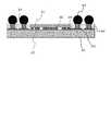
本発明による半導体装置は、上記実施形態に限定されるものではなく、様々な変形が可能である。例えば、図7に示すように、本発明による半導体装置は、半導体チップ10の面S1とは反対側に設けられ、ワイヤボンディングにより半導体チップ10と接続されたパッケージ基板80と、半導体チップ10とは反対側のパッケージ基板80上に設けられた外部電極端子82と、を備えていてもよい。同図においては、半導体チップ10がパッケージ基板80上に載置されている。半導体チップ10上の配線40には、ワイヤ84の一端が接続されている。ワイヤ84の他端は、パッケージ基板80上の電極パッド(図示せず)に接続されている。また、パッケージ基板80上には、半導体チップ10,20を覆うモールド樹脂86が形成されている。 The semiconductor device according to the present invention is not limited to the above embodiment, and various modifications are possible. For example, as shown in FIG. 7, the semiconductor device according to the present invention includes a package substrate 80 provided on the side opposite to the surface S1 of the
また、上記各実施形態においては導体ポスト42と外部電極端子64とが配線層60を介して接続された例を示したが、図8に示すように、導体ポスト42と外部電極端子64とは互いに直接接続されていてもよい。 In the above embodiments, the
上記各実施形態においては半導体チップ20の側面および上面が共に絶縁性樹脂層50によって覆われた例を示したが、半導体チップ20の側面のみが絶縁性樹脂層50によって覆われた構成としてもよい。すなわち、半導体チップ20の上面が絶縁性樹脂層50の表面に露出していてもよい。 In each of the above embodiments, the example in which the side surface and the top surface of the
1 半導体装置
2 半導体装置
10,20 半導体チップ
30 シールリング
32,34 導電部材
40 配線
42 導体ポスト
50 絶縁性樹脂層
60 配線層
62 配線
64 外部電極端子
70 絶縁膜
80 パッケージ基板
82 外部電極端子
84 ワイヤ
86 モールド樹脂DESCRIPTION OF
Claims (4)
Translated fromJapanese前記第1の半導体チップと所定の間隔を置いて、当該第1の半導体チップの一面上に設けられた第2の半導体チップと、
前記第1および第2の半導体チップ間に介在するシールリングと、を備え、
前記第1および第2の半導体チップ間には、前記シールリングの内側の領域である内部領域と、前記シールリングの外側の領域である外部領域とが設けられており、
前記内部領域に設けられ、前記第1および第2の半導体チップを電気的に接続する第1の導電部材と、
前記外部領域に設けられ、前記第1および第2の半導体チップを電気的に接続する第2の導電部材と、
を備え、
前記第1の半導体チップは、前記第2の半導体チップよりも面積が大きく、
前記第1の半導体チップの前記一面とは反対側に設けられ、ワイヤボンディングにより当該第1の半導体チップと接続されたパッケージ基板と、
前記第1の半導体チップとは反対側の前記パッケージ基板上に設けられた外部電極端子と、を備える半導体装置。A first semiconductor chip;
A second semiconductor chip provided on one surface of the first semiconductor chip at a predetermined interval from the first semiconductor chip;
A seal ring interposed between the first and second semiconductor chips,
Between the first and second semiconductor chips, an inner region that is an inner region of the seal ring and an outer region that is an outer region of the seal ring are provided,
A first conductive member provided in the inner region and electrically connecting the first and second semiconductor chips;
A second conductive member provided in the external region and electrically connecting the first and second semiconductor chips;
Equipped witha,
The first semiconductor chip has a larger area than the second semiconductor chip,
A package substrate provided on the opposite side of the one surface of the first semiconductor chip and connected to the first semiconductor chip by wire bonding;
Wherein the external electrode terminal and the first semiconductor chip on the opposite side of the package substrate, the semiconductor device Rucomprising a.
前記第1の半導体チップの前記一面上に設けられた配線を備え、
当該配線に前記第2の導電部材が接続されている半導体装置。The semiconductor device according to claim 1,
A wiring provided on the one surface of the first semiconductor chip;
A semiconductor device in which the second conductive member is connected to the wiring.
前記配線の一部は、絶縁膜を介して前記第1の半導体チップの前記一面上に設けられている半導体装置。The semiconductor device according to claim 2,
A part of the wiring is a semiconductor device provided on the one surface of the first semiconductor chip via an insulating film.
前記絶縁膜は、有機絶縁膜である半導体装置。The semiconductor device according to claim 3.
The semiconductor device, wherein the insulating film is an organic insulating film.
Priority Applications (2)
| Application Number | Priority Date | Filing Date | Title |
|---|---|---|---|
| JP2005294710AJP4834369B2 (en) | 2005-10-07 | 2005-10-07 | Semiconductor device |
| US11/542,128US8039969B2 (en) | 2005-10-07 | 2006-10-04 | Semiconductor device |
Applications Claiming Priority (1)
| Application Number | Priority Date | Filing Date | Title |
|---|---|---|---|
| JP2005294710AJP4834369B2 (en) | 2005-10-07 | 2005-10-07 | Semiconductor device |
Related Child Applications (1)
| Application Number | Title | Priority Date | Filing Date |
|---|---|---|---|
| JP2011130903ADivisionJP5466203B2 (en) | 2011-06-13 | 2011-06-13 | Semiconductor device |
Publications (2)
| Publication Number | Publication Date |
|---|---|
| JP2007103839A JP2007103839A (en) | 2007-04-19 |
| JP4834369B2true JP4834369B2 (en) | 2011-12-14 |
Family
ID=37944414
Family Applications (1)
| Application Number | Title | Priority Date | Filing Date |
|---|---|---|---|
| JP2005294710AExpired - Fee RelatedJP4834369B2 (en) | 2005-10-07 | 2005-10-07 | Semiconductor device |
Country Status (2)
| Country | Link |
|---|---|
| US (1) | US8039969B2 (en) |
| JP (1) | JP4834369B2 (en) |
Families Citing this family (8)
| Publication number | Priority date | Publication date | Assignee | Title |
|---|---|---|---|---|
| KR100925665B1 (en)* | 2007-12-10 | 2009-11-06 | 주식회사 네패스 | System-in-package and its manufacturing method |
| US8618670B2 (en) | 2008-08-15 | 2013-12-31 | Qualcomm Incorporated | Corrosion control of stacked integrated circuits |
| JP6342033B2 (en)* | 2010-06-30 | 2018-06-13 | キヤノン株式会社 | Solid-state imaging device |
| JP2012033894A (en) | 2010-06-30 | 2012-02-16 | Canon Inc | Solid state image sensor |
| TWI491009B (en)* | 2010-10-08 | 2015-07-01 | Chip level emi shielding structure and manufacture method thereof | |
| FR3029013A1 (en)* | 2014-11-21 | 2016-05-27 | Stmicroelectronics (Grenoble 2) Sas | ELECTRONIC DEVICE COMPRISING STACKED CHIPS |
| US9773740B2 (en) | 2014-11-26 | 2017-09-26 | Stmicroelectronics (Grenoble 2) Sas | Stacked electronic device including a protective wafer bonded to a chip by an infused adhesive |
| US10475767B2 (en) | 2018-01-04 | 2019-11-12 | Kabushiki Kaisha Toshiba | Electronic device |
Family Cites Families (15)
| Publication number | Priority date | Publication date | Assignee | Title |
|---|---|---|---|---|
| JPS5290268A (en)* | 1976-01-23 | 1977-07-29 | Hitachi Ltd | Semiconductor device |
| JPS6189657A (en)* | 1984-10-08 | 1986-05-07 | Matsushita Electric Ind Co Ltd | Semiconductor device and its manufacturing method |
| JPH0430544A (en)* | 1990-05-28 | 1992-02-03 | Hitachi Ltd | Semiconductor integrated circuit device |
| EP0951068A1 (en)* | 1998-04-17 | 1999-10-20 | Interuniversitair Micro-Elektronica Centrum Vzw | Method of fabrication of a microstructure having an inside cavity |
| JP3321427B2 (en)* | 1999-02-10 | 2002-09-03 | ローム株式会社 | Semiconductor device |
| US6853067B1 (en)* | 1999-10-12 | 2005-02-08 | Microassembly Technologies, Inc. | Microelectromechanical systems using thermocompression bonding |
| US6750521B1 (en)* | 1999-10-22 | 2004-06-15 | Delphi Technologies, Inc. | Surface mount package for a micromachined device |
| US20020096421A1 (en)* | 2000-11-29 | 2002-07-25 | Cohn Michael B. | MEMS device with integral packaging |
| JP4593835B2 (en) | 2001-07-04 | 2010-12-08 | パナソニック株式会社 | Semiconductor device and manufacturing method thereof |
| JP2004128288A (en)* | 2002-10-04 | 2004-04-22 | Renesas Technology Corp | Semiconductor device and electronic apparatus |
| US7335971B2 (en)* | 2003-03-31 | 2008-02-26 | Robert Bosch Gmbh | Method for protecting encapsulated sensor structures using stack packaging |
| US7294919B2 (en)* | 2003-11-26 | 2007-11-13 | Avago Technologies General Ip (Singapore) Pte. Ltd. | Device having a complaint element pressed between substrates |
| JP4095049B2 (en)* | 2004-08-30 | 2008-06-04 | シャープ株式会社 | High reliability semiconductor device using electrode hermetic sealing |
| KR100498708B1 (en)* | 2004-11-08 | 2005-07-01 | 옵토팩 주식회사 | Electronic package for semiconductor device and packaging method thereof |
| US7262622B2 (en)* | 2005-03-24 | 2007-08-28 | Memsic, Inc. | Wafer-level package for integrated circuits |
- 2005
- 2005-10-07JPJP2005294710Apatent/JP4834369B2/ennot_activeExpired - Fee Related
- 2006
- 2006-10-04USUS11/542,128patent/US8039969B2/ennot_activeExpired - Fee Related
Also Published As
| Publication number | Publication date |
|---|---|
| US8039969B2 (en) | 2011-10-18 |
| US20070080467A1 (en) | 2007-04-12 |
| JP2007103839A (en) | 2007-04-19 |
Similar Documents
| Publication | Publication Date | Title |
|---|---|---|
| US10276553B2 (en) | Chip package structure and manufacturing method thereof | |
| US7871925B2 (en) | Stack package and method for manufacturing the same | |
| JP5118942B2 (en) | Through-silicon via stack package and manufacturing method thereof | |
| US6642627B2 (en) | Semiconductor chip having bond pads and multi-chip package | |
| US12074137B2 (en) | Multi-chip package and manufacturing method thereof | |
| US20090278243A1 (en) | Stacked type chip package structure and method for fabricating the same | |
| US8039969B2 (en) | Semiconductor device | |
| KR100842921B1 (en) | Manufacturing method of semiconductor package | |
| US7122748B2 (en) | Semiconductor device having packaging structure | |
| KR20150091933A (en) | Manufacturing method of semiconductor device and semiconductor device thereof | |
| WO2007026392A1 (en) | Semiconductor device and method for manufacturing same | |
| JP5358089B2 (en) | Semiconductor device | |
| US7939379B2 (en) | Hybrid carrier and a method for making the same | |
| US11183483B2 (en) | Multichip module and electronic device | |
| US20090115036A1 (en) | Semiconductor chip package having metal bump and method of fabricating same | |
| US20150084171A1 (en) | No-lead semiconductor package and method of manufacturing the same | |
| JP2003318360A (en) | Semiconductor device and method of manufacturing the same | |
| US20060267190A1 (en) | Semiconductor device, laminated semiconductor device, and method for producing semiconductor device | |
| JP5466203B2 (en) | Semiconductor device | |
| TW202137342A (en) | Chip embedded substrate structure, chip package structure and methods of manufacture thereof | |
| TWI582903B (en) | Semiconductor package structure and maufacturing method thereof | |
| TWI590349B (en) | Chip package and chip packaging process | |
| CN119008565B (en) | Fan-out packaging structure and method for preparing the fan-out packaging structure | |
| US20250062237A1 (en) | Semiconductor package | |
| US20240315054A1 (en) | Upside-Down DRAM Package Structure |
Legal Events
| Date | Code | Title | Description |
|---|---|---|---|
| A621 | Written request for application examination | Free format text:JAPANESE INTERMEDIATE CODE: A621 Effective date:20080917 | |
| A977 | Report on retrieval | Free format text:JAPANESE INTERMEDIATE CODE: A971007 Effective date:20100910 | |
| A131 | Notification of reasons for refusal | Free format text:JAPANESE INTERMEDIATE CODE: A131 Effective date:20100914 | |
| A521 | Request for written amendment filed | Free format text:JAPANESE INTERMEDIATE CODE: A523 Effective date:20101028 | |
| A131 | Notification of reasons for refusal | Free format text:JAPANESE INTERMEDIATE CODE: A131 Effective date:20110419 | |
| A521 | Request for written amendment filed | Free format text:JAPANESE INTERMEDIATE CODE: A523 Effective date:20110613 | |
| A131 | Notification of reasons for refusal | Free format text:JAPANESE INTERMEDIATE CODE: A131 Effective date:20110705 | |
| A521 | Request for written amendment filed | Free format text:JAPANESE INTERMEDIATE CODE: A523 Effective date:20110830 | |
| TRDD | Decision of grant or rejection written | ||
| A01 | Written decision to grant a patent or to grant a registration (utility model) | Free format text:JAPANESE INTERMEDIATE CODE: A01 Effective date:20110920 | |
| A01 | Written decision to grant a patent or to grant a registration (utility model) | Free format text:JAPANESE INTERMEDIATE CODE: A01 | |
| A61 | First payment of annual fees (during grant procedure) | Free format text:JAPANESE INTERMEDIATE CODE: A61 Effective date:20110926 | |
| R150 | Certificate of patent or registration of utility model | Ref document number:4834369 Country of ref document:JP Free format text:JAPANESE INTERMEDIATE CODE: R150 Free format text:JAPANESE INTERMEDIATE CODE: R150 | |
| FPAY | Renewal fee payment (event date is renewal date of database) | Free format text:PAYMENT UNTIL: 20140930 Year of fee payment:3 | |
| S531 | Written request for registration of change of domicile | Free format text:JAPANESE INTERMEDIATE CODE: R313531 | |
| R350 | Written notification of registration of transfer | Free format text:JAPANESE INTERMEDIATE CODE: R350 | |
| LAPS | Cancellation because of no payment of annual fees |