JP4833586B2 - Semiconductor integrated circuit with built-in data cache and its actual speed test method - Google Patents
Semiconductor integrated circuit with built-in data cache and its actual speed test methodDownload PDFInfo
- Publication number
- JP4833586B2 JP4833586B2JP2005162840AJP2005162840AJP4833586B2JP 4833586 B2JP4833586 B2JP 4833586B2JP 2005162840 AJP2005162840 AJP 2005162840AJP 2005162840 AJP2005162840 AJP 2005162840AJP 4833586 B2JP4833586 B2JP 4833586B2
- Authority
- JP
- Japan
- Prior art keywords
- address
- data
- data cache
- chip memory
- cache
- Prior art date
- Legal status (The legal status is an assumption and is not a legal conclusion. Google has not performed a legal analysis and makes no representation as to the accuracy of the status listed.)
- Expired - Fee Related
Links
Images


Classifications
- G—PHYSICS
- G06—COMPUTING OR CALCULATING; COUNTING
- G06F—ELECTRIC DIGITAL DATA PROCESSING
- G06F12/00—Accessing, addressing or allocating within memory systems or architectures
- G06F12/02—Addressing or allocation; Relocation
- G06F12/08—Addressing or allocation; Relocation in hierarchically structured memory systems, e.g. virtual memory systems
- G—PHYSICS
- G06—COMPUTING OR CALCULATING; COUNTING
- G06F—ELECTRIC DIGITAL DATA PROCESSING
- G06F11/00—Error detection; Error correction; Monitoring
- G06F11/22—Detection or location of defective computer hardware by testing during standby operation or during idle time, e.g. start-up testing
- G06F11/24—Marginal checking or other specified testing methods not covered by G06F11/26, e.g. race tests
- G—PHYSICS
- G11—INFORMATION STORAGE
- G11C—STATIC STORES
- G11C29/00—Checking stores for correct operation ; Subsequent repair; Testing stores during standby or offline operation
- G11C29/04—Detection or location of defective memory elements, e.g. cell constructio details, timing of test signals
- G11C29/08—Functional testing, e.g. testing during refresh, power-on self testing [POST] or distributed testing
- G—PHYSICS
- G11—INFORMATION STORAGE
- G11C—STATIC STORES
- G11C29/00—Checking stores for correct operation ; Subsequent repair; Testing stores during standby or offline operation
- G11C29/04—Detection or location of defective memory elements, e.g. cell constructio details, timing of test signals
- G11C2029/0401—Detection or location of defective memory elements, e.g. cell constructio details, timing of test signals in embedded memories
- G—PHYSICS
- G11—INFORMATION STORAGE
- G11C—STATIC STORES
- G11C29/00—Checking stores for correct operation ; Subsequent repair; Testing stores during standby or offline operation
- G11C29/04—Detection or location of defective memory elements, e.g. cell constructio details, timing of test signals
- G11C29/08—Functional testing, e.g. testing during refresh, power-on self testing [POST] or distributed testing
- G11C29/12—Built-in arrangements for testing, e.g. built-in self testing [BIST] or interconnection details
- G11C29/18—Address generation devices; Devices for accessing memories, e.g. details of addressing circuits
- G11C2029/1806—Address conversion or mapping, i.e. logical to physical address
Landscapes
- Engineering & Computer Science (AREA)
- Theoretical Computer Science (AREA)
- General Engineering & Computer Science (AREA)
- Physics & Mathematics (AREA)
- General Physics & Mathematics (AREA)
- Computer Hardware Design (AREA)
- Quality & Reliability (AREA)
- Memory System Of A Hierarchy Structure (AREA)
- For Increasing The Reliability Of Semiconductor Memories (AREA)
- Tests Of Electronic Circuits (AREA)
- Techniques For Improving Reliability Of Storages (AREA)
- Test And Diagnosis Of Digital Computers (AREA)
Description
Translated fromJapanese本発明は半導体集積回路のテストに係わり、さらに具体的には半導体集積回路に内蔵されたデータキャッシュのための実速度テスト装置および方法に関する。 The present invention relates to a test of a semiconductor integrated circuit, and more particularly to an actual speed test apparatus and method for a data cache incorporated in a semiconductor integrated circuit.
半導体工程が発展することによって、最近開発されている半導体集積回路は中央処理装置(Central Processing Unit;CPU)とキャッシュメモリが単一チップで集積されたSOC(system on a chip)形態に開発される傾向を示している。CPUとキャッシュメモリを単一チップとして集積する場合、データ入/出力速度が向上し、その結果、CPUの全体性能が向上する効果を得ることができる。しかし、製造工程の不均衡などによって半導体集積回路に不良が発生する場合があり、このような不良を検出するためには半導体集積回路の実際動作速度に合わせてテストを実行する実速度テスト(at speed test)が多用されている。 With the development of semiconductor processes, recently developed semiconductor integrated circuits are developed in the form of an SOC (system on a chip) in which a central processing unit (CPU) and a cache memory are integrated on a single chip. It shows a trend. When the CPU and the cache memory are integrated as a single chip, the data input / output speed is improved, and as a result, the effect of improving the overall performance of the CPU can be obtained. However, a defect may occur in the semiconductor integrated circuit due to an imbalance in the manufacturing process, and in order to detect such a defect, an actual speed test (at) that executes a test in accordance with the actual operation speed of the semiconductor integrated circuit. speed test) is frequently used.
現在主に使用されている実速度テスト用テスタの動作周波数は約80MHz程度であるのに比べて、半導体集積回路の動作周波数は100MHz以上から1GHzを超過する場合もある。最近には300MHz以上の高速動作が可能なテスタが登場しているが、非常に高価であり、高速のテスタを利用してもテスタと半導体集積回路とを連結させる複数個の外部ピン(すなわち、外部端子)に存在するピン間の寄生容量によって動作周波数に影響を及ぼすようになる。 The operating frequency of the actual speed test tester mainly used at present is about 80 MHz, whereas the operating frequency of the semiconductor integrated circuit may be 100 MHz or more to exceed 1 GHz. Recently, a tester capable of operating at a high speed of 300 MHz or more has appeared, but it is very expensive, and even if a high-speed tester is used, a plurality of external pins that connect the tester and the semiconductor integrated circuit (that is, The operating frequency is affected by the parasitic capacitance between pins existing in the external terminal.
このような問題を解決するため、半導体集積回路の内部的では高速のオンチップPLLクロック(On−chip PLL(Phase−Locked Loop)clock)を使用して高速のテストを実行し、テスト結果だけ低速のテスタに伝送して確認する方法が使用されている。この場合、テストパターンは半導体集積回路の外部に位置したオフチップメモリ(off−chip memory)または内部に位置したオンチップメモリ(on−chip memory)に貯蔵されることができ、システムの性能を低下させず、最適の実速度テストを実行するためにはオフチップメモリよりはオンチップメモリを使用することより望ましい。 In order to solve such a problem, a high-speed on-chip PLL clock (On-chip PLL (Phase-Locked Loop) clock) is used internally in the semiconductor integrated circuit, and only the test result is slow. A method of transmitting to a tester and checking it is used. In this case, the test pattern can be stored in an off-chip memory located outside the semiconductor integrated circuit or an on-chip memory located inside, thereby degrading the performance of the system. Instead, it is more desirable to use on-chip memory than off-chip memory to perform the optimal real speed test.
特許文献1にはテスタによってオンチップメモリにあらかじめ貯蔵されたテストパターンを利用して集積回路の内部で自体的に実速度テストを実行し、テスト実行の結果を外部の低速テスタへ伝送する技術が開示されている。しかし、前記テスト方法でデータキャッシュの全領域の動作を十分にテストするためには、必ずデータキャッシュ(data cache)サイズより大きいオンチップメモリが集積回路内に具備されなければならないので、半導体集積回路のサイズが大きくなり、集積度が低下することがある。
本発明の課題は、データキャッシュサイズより小さいオンチップメモリを有しても半導体集積回路に内蔵されたデータキャッシュを実速度テストすることができる装置および方法を提供することにある。 SUMMARY OF THE INVENTION An object of the present invention is to provide an apparatus and a method capable of performing an actual speed test on a data cache incorporated in a semiconductor integrated circuit even if it has an on-chip memory smaller than the data cache size.
本発明の目的を達成するために本発明の特徴によれば、半導体集積回路は、 第1データ貯蔵領域を有するデータキャッシュと、前記データキャッシュの前記第1データ貯蔵領域より小さい第2データ貯蔵領域を有し、テストデータを貯蔵するオンチップメモリと、前記オンチップメモリに貯蔵された前記テストデータに対するアクセスが要求される時、前記第1データ貯蔵領域が前記第2貯蔵領域にマッピングされるようにアドレスをデコーディングするアドレスデコーダとを含むことを特徴とする。 In order to achieve the object of the present invention, according to a feature of the present invention, a semiconductor integrated circuit includes a data cache having a first data storage area, and a second data storage area smaller than the first data storage area of the data cache. And when the access to the test data stored in the on-chip memory is requested, the first data storage area is mapped to the second storage area. And an address decoder for decoding the address.
本発明の目的を達成するために本発明の特徴によれば、半導体集積回路のための実速度テストシステムは、データキャッシュのデータ貯蔵領域が前記データキャッシュより小さいデータ貯蔵領域を有するオンチップメモリにマッピングされるようにアドレスをデコーディングし、前記オンチップメモリに貯蔵されたテストデータを利用して前記デコーディングされたアドレス別に前記データキャッシュに対するリード−ミス、書き込み−ミス、ラインフィルおよびキャストアウト動作を実行する半導体集積回路と、前記半導体集積回路の外部で前記データキャッシュの動作実行の結果を受け入れて前記データキャッシュの欠陥の可否を分析するテスト回路とを含むことを特徴とする。 According to a feature of the present invention for achieving the object of the present invention, an actual speed test system for a semiconductor integrated circuit is implemented in an on-chip memory having a data storage area of a data cache smaller than the data cache. Decode addresses to be mapped, read-miss, write-miss, line fill and cast-out operations to the data cache for each decoded address using test data stored in the on-chip memory And a test circuit that receives a result of the operation of the data cache outside the semiconductor integrated circuit and analyzes whether the data cache is defective or not.
本発明の目的を達成するために本発明の特徴によれば、半導体集積回路に内蔵されたオンチップメモリを利用してデータキャッシュを実速度テストする方法は、(a)前記データキャッシュのアドレス領域を前記データキャッシュより小さい前記オンチップメモリのアドレス領域にデコーディングする段階と、(b)前記デコーディングされたアドレスに応答して前記オンチップメモリからテストデータを読み込んで前記データキャッシュのリード−ミス、書き込み−ミス、ラインフィルおよびキャストアウトをテストする段階とを含むことを特徴とする。 In order to achieve the object of the present invention, according to a feature of the present invention, a method for testing a data cache at an actual speed using an on-chip memory built in a semiconductor integrated circuit includes: (a) an address area of the data cache; In the address area of the on-chip memory smaller than the data cache, and (b) reading test data from the on-chip memory in response to the decoded address to read-miss the data cache Write-miss, line fill, and castout testing steps.
本発明の目的を達成するために本発明の特徴によれば、半導体集積回路に内蔵されたオンチップメモリを利用してデータキャッシュを実速度テストする方法は、(a)前記データキャッシュのアドレス領域を前記データキャッシュより小さい前記オンチップメモリのアドレス領域にデコーディングする段階と、(b)前記デコーディングされたアドレスに応答して前記オンチップメモリからテストデータを読み込んで前記データキャッシュに対するリード−ミス、書き込み−ミス、ラインフィルおよびキャストアウト動作を実行し、前記実行の結果を前記半導体集積回路の外部のテスト装置に出力する段階と、(c)前記テスト装置で前記データキャッシュの動作実行の結果を分析して前記データキャッシュの欠陥の可否を判断する段階とを含む。 In order to achieve the object of the present invention, according to a feature of the present invention, a method for testing a data cache at an actual speed using an on-chip memory built in a semiconductor integrated circuit includes: (a) an address area of the data cache; And (b) reading test data from the on-chip memory in response to the decoded address and reading-missing the data cache. Executing a write-miss, line fill, and castout operation, and outputting the execution result to a test device outside the semiconductor integrated circuit; and (c) a result of executing the data cache operation in the test device. Analyzing the data cache and determining whether the data cache is defective or not. No.
望ましい実施形態において、前記データキャッシュがN個のアドレスを有する場合、2N個のアドレスを前記オンチップメモリのアドレス領域にデコーディングし、前記データキャッシュのアドレスビットのうちの少なくとも一つの以上がアドレスデコーディング時、考慮されないドントケアアドレスビット(don’t care address bits)として使用されることを特徴とする。 In a preferred embodiment, when the data cache has N addresses, 2N addresses are decoded into the address area of the on-chip memory, and at least one of the address bits of the data cache is address-decoded. It is characterized in that it is used as don't care address bits that are not considered when coding.
望ましい実施形態において、前記データキャッシュが2n個のセットを有し、各々のセットが2s個のブロックを有し、一つのキャッシュブロックサイズが2bバイトであり、全体キャッシュサイズが2(s+b+n)バイトであり、前記オンチップメモリが単一セットサイズに該当する2(s+b)バイトのアドレス領域を有する場合、前記ドントケアアドレスビットにn+1ビットが割り当てられ、前記オンチップメモリが単一ブロックサイズに該当する2bバイトのアドレス領域を有する場合、前記ドントケアアドレスビットにn+s+1ビットが割り当てられることを特徴とする。In a preferred embodiment, the data cache has 2n sets, each set has 2s blocks, one cache block size is 2b bytes, and the total cache size is 2(s + b + n ) Bytes, and when the on-chip memory has an address area of 2(s + b) bytes corresponding to a single set size, n + 1 bits are allocated to the don't care address bits, and the on-chip memory is a single block. when having 2b bytes of the address area corresponding to the size, characterized in that n + s + 1 bit is assigned to the do not care address bits.
本発明によれば、データキャッシュの各アドレスがオンチップメモリの各々の他のアドレスにデコーディングされるのに代えて、データキャッシュの複数個のアドレスが一定アドレス単位ごとにオンチップメモリの一つのアドレスにデコーディングされる。そしてデコーディングされたアドレスを使用してデータキャッシュの全体アドレス領域に対するリード−ミス、書き込み−ミス、リード−ミスおよびキャストアウト動作を全部テストすることができるので、データキャッシュより小さいサイズを有するオンチップメモリを有しも半導体集積回路に内蔵されているデータキャッシュに対する実速度テストを十分に実行することができる。 According to the present invention, instead of decoding each address of the data cache into each other address of the on-chip memory, a plurality of addresses of the data cache are stored in one on-chip memory for each predetermined address unit. Decoded to an address. Since the decoded address can be used to test all read-miss, write-miss, read-miss and castout operations for the entire address area of the data cache, the on-chip has a smaller size than the data cache. An actual speed test can be sufficiently performed on a data cache having a memory and built in a semiconductor integrated circuit.
以下、本発明による実施形態を添付の図を参照して詳細に説明する。 Hereinafter, embodiments of the present invention will be described in detail with reference to the accompanying drawings.
本発明の新規したデータキャッシュが内蔵された半導体集積回路およびそれの実速度テスト方法は、データキャッシュのアドレスデコーディング時、一定ビットを考慮しなくデコーディングを実行して、データキャッシュの複数個のアドレスを所定のアドレス単位ごとにオンチップメモリの一つのアドレスにマッピングする。そして、デコーディングされたアドレスを利用してデータキャッシュのN個の互いに異なるアドレスに対するN回のリード−ミス(read−miss)、N回の書き込み−ミス(write−miss)、そしてN回のラインフィルおよびキャストアウト動作に対するテストを全部実行する。その結果、データキャッシュより小さいサイズを有するオンチップメモリを有してもデータキャッシュに対する実速度テストを十分に実行することができるようになる。 A semiconductor integrated circuit incorporating a new data cache of the present invention and an actual speed test method thereof perform a plurality of data caches by performing decoding without considering a certain bit when data cache addresses are decoded. The address is mapped to one address of the on-chip memory for each predetermined address unit. Then, using the decoded address, N read-misses, N write-misses, and N lines for N different addresses of the data cache. Perform all tests for fill and castout operations. As a result, even if an on-chip memory having a smaller size than the data cache is provided, the actual speed test for the data cache can be sufficiently performed.
図1は本発明が適用される半導体集積回路100のブロック図として、半導体集積回路100とテスタ10との連結関係が示している。 FIG. 1 is a block diagram of a semiconductor integrated
図1を参照すれば、本発明による半導体集積回路100はデータキャッシュ110と、データキャッシュ110が内蔵されたCPU(Central Processing Unit)120と、半導体集積回路100を動作させるのに必要な高速のクロック信号を発生するPLL130と、半導体集積回路100に内蔵されたオンチップメモリ140と、オンチップメモリ140の入出力動作を制御するメモリコントローラ150と、データキャッシュ110より小さいオンチップメモリ140でもデータキャッシュ110のすべての機能を十分にテストするように類似アドレス(synonym address)をデコーディングする類似アドレスデコーダ160と、複数個のロジックブロック180と、半導体集積回路100に具備された機能ブロックの間で信号およびデータを伝達するバス190とを含む。 Referring to FIG. 1, a semiconductor integrated
図1に示したように、最近開発されている半導体集積回路、いわゆるSOC(system on a chip)は数百MHzで動作するキャッシュ内蔵型CPU120と、100MHz以上で動作するメモリコントローラ150などを具備している。高速SOCの最大遅延経路(critical timing path)ではキャッシュラインフィル(cache line fill)とビクティムキャストアウト(victim cast out)があり、このような最大遅延経路をクロックを直接印加して実速度テストするのにはIO(Input Output)特性上、様々な難しさが伴うので、本発明では数百MHzのクロックを外部テスタ10で印加するに代えて内部PLL130で発生された高速クロック信号を使用してSOCをテストし、データキャッシュ110より小さいサイズのオンチップメモリ140を利用してテストを実行するように類似アドレスデコーダ160からデコーディングされた類似アドレス(synonym address)を利用してテストを実行する。すなわち、CPU120はキャッシュミス時、オンチップメモリ140に貯蔵されたテストデータを読み込んでデータキャッシュ110のN個の互いに異なるアドレスに対するN回のリード−ミス(read−miss)、N回の書き込み−ミス(write−miss)、N回のラインフィルおよびキャストアウト動作を実行する。そして、前記動作実行の結果は半導体集積回路100の外部に連結されたテスタ10に伝送されて、テスト結果が判断される。その結果、低速のテスタ10を利用して高速の半導体集積回路100をテストし、データキャッシュ110より小さいサイズのオンチップメモリ140を有して半導体集積回路100に対するテストを十分に実行することができるようになる。 As shown in FIG. 1, a recently developed semiconductor integrated circuit, so-called SOC (system on a chip), includes a
一般的に、半導体集積回路100の性能は回路内の可能なすべての信号伝達経路(signal propagation path)のうちの最も長い経路によって決められ、これによって回路の性能が決められるので、これを最大遅延経路または臨界経路と言う。したがって、下では図1に示した半導体集積回路100の最大遅延経路、すなわちデータキャッシュ110のキャッシュラインフィル(cache line fill)とビクティムキャストアウト(victim cast out)に対して説明するためにデータキャッシュ110に対する基本構造を説明する。 In general, the performance of the semiconductor integrated
プログラムを分析すれば、与えられた時間の間最近書き込んだデータや命令語を再書き込みする傾向を有している。これを参照の地域性(locality of reference)という。このような現象はコンピュータプログラムでプログラムループとサブルーチンが多用されており、分岐命令語に接する前まで命令語が順次に要請されるという事実から容易に理解されることができる。このように、よく参照されるプログラムとデータは速度が速いキャッシュメモリに貯蔵される。CPUはメモリに接近する必要がある時、まずキャッシュを調査した後、所望するワードがキャッシュから発見されれば、これを読み込み、発見されなければ、メインメモリに接近する。CPUが参照しようとするデータや命令語がキャッシュに存在すれば、これをキャッシュヒット(cache hit)といい、キャッシュに存在しなければ、これをキャッシュミス(cache miss)という。キャッシュヒットが発生すれば、待機時間なしにCPUが動作することができるが、キャッシュミスが発生すれば、メモリまで行ってデータや命令語を参照しなければならないので、時間遅延が発生するようになる。 If a program is analyzed, it has a tendency to rewrite recently written data and instruction words for a given time. This is referred to as locality of reference. Such a phenomenon can be easily understood from the fact that a program loop and a subroutine are frequently used in a computer program, and instruction words are sequentially requested before contacting a branch instruction word. In this way, frequently referenced programs and data are stored in a fast cache memory. When the CPU needs to access the memory, it first examines the cache, then reads if the desired word is found from the cache, and if not found, it approaches the main memory. If data or an instruction word to be referred to by the CPU exists in the cache, this is called a cache hit, and if it does not exist in the cache, this is called a cache miss. If a cache hit occurs, the CPU can operate without waiting time. However, if a cache miss occurs, the memory and the instruction word must be referred to the memory so that a time delay occurs. Become.
キャッシュメモリの基本的な特性は速い接近時間として、キャッシュで必要なデータを捜すのにほとんど時間がかからないようにしなければならない。メインメモリからキャッシュメモリにデータを伝送することをマッピングプロセスといい、マッピングプロセスの種類によって、キャッシュは、完全アソシアティブキャッシュ(Fully associativeキャッシュ)、ダイレクトマッピングキャッシュ(Direct mapped cache)、およびN−ウェイセット−アソシアティブキャッシュ(N−way set−associative cache)に区分される。 The basic characteristic of a cache memory is fast access time, so that it takes almost no time to search for the necessary data in the cache. Transfer of data from the main memory to the cache memory is called a mapping process. Depending on the type of the mapping process, the cache may be a fully associative cache, a direct mapped cache, or an N-way set. It is divided into associative caches (N-way set-associative caches).
図2は図1に示したデータキャッシュ110の構造を示す図であり、N―ウェイセットアソシアティブデータキャッシュ(N−way set associative data cache)の論理的構造が示している。 FIG. 2 is a diagram illustrating a structure of the
N−ウェイセット−アソシアティブキャッシュは、キャッシュメモリ内の一つのエントリーにマッピングされることができるブロックを一つのセット(set)に縛ったことを意味する。例えば、2−ウェイセット−アソシアティブキャッシュは同一のブロックインデックス(block index)を有するブロックがキャッシュメモリに二つ貯蔵されることができるということを意味する。この場合、ダイレクトマッピングキャッシュよりミス率(miss rate)を減らすことができるという長所があり、ダイレクトマッピングキャッシュは1−ウェイセット−アソシアティブキャッシュともいえる。 N-way set-associative cache means that a block that can be mapped to one entry in the cache memory is bound to one set. For example, 2-way set-associative cache means that two blocks having the same block index can be stored in the cache memory. In this case, there is an advantage that a miss rate can be reduced as compared with the direct mapping cache, and the direct mapping cache can be said to be a 1-way set-associative cache.
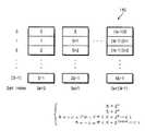
図2を参照すれば、N−ウェイセット−アソシアティブキャッシュで構成されたデータキャッシュ110はN個(すなわち、2n個)のセットを有し、各々のセットはS個(すなわち2s個)のブロックを有する。 ここで、一つのキャッシュブロックサイズは2bバイトであり、全体キャッシュサイズは2(s+b+n)バイトである。例えば、ARM社のARM1020Eは32Kbytesのデータ(すなわち、32Kbytes =215=2(s+b+n)=2(4+5+6))を有し、64−ウェイセット−アソシアティブ、32バイトブロック構造で構成される。したがって、ARM社のARM1020Eのデータキャッシュのパラメータ値は各々N=64、n=6(64=2nであるので、n=6)、S=16、s=4(16=2sであるので、s=4)、b=5(32=2bであるので、b=5)と同様である。ARM社のARM1020Eに対するより詳細な構成は2002年ARM社で発行された“ARM1020E Technical Reference Manual”に詳細に開示されている。Referring to FIG. 2, the
図3は図2に示した構造を有するデータキャッシュ110のキャッシュミス発生例を示す図である。 FIG. 3 is a diagram showing an example of occurrence of a cache miss in the
図3を参照すれば、同一のセットインデックス(set index)Kを有し、かつ互いに異なるアドレスを有するN+1個のデータアクセス(data access)は、データキャッシュミス(data cache miss)を誘発するようになることが分かる。例えば、ARM1020Eデータキャッシュの場合、address[8:5]が同一の65個の互いに異なるアドレスデータをアクセスすれば、データキャッシュミスが発生するようになる。下で詳細に説明するが、本発明では、キャッシュミスの発生時、類似アドレスをデコーディングし、これを利用してテストを実行するようになる。類似アドレスのデコーディング方法は次のとおりである。 Referring to FIG. 3, N + 1 data accesses having the same set index K and different addresses may induce a data cache miss. I understand that For example, in the case of the ARM1020E data cache, if 65 different address data having the same address [8: 5] are accessed, a data cache miss occurs. As will be described in detail below, in the present invention, when a cache miss occurs, a similar address is decoded and a test is executed using this. The decoding method of similar addresses is as follows.
図4および図5は図1に示した類似アドレスデコーダ160のアドレスデコーディング例を示す図である。 4 and 5 are diagrams showing an example of address decoding of the
従来にはデータキャッシュ110の各アドレスがオンチップメモリ140の各々の他のアドレスにデコーディングされなければならないので、テストしようとするデータキャッシュ110より大きいオンチップメモリ140が必ず具備されなければならなかった。しかし、本発明では、データキャッシュ110の各アドレスをオンチップメモリ140の各々の他のアドレスにデコーディングするに代えて、一定アドレス単位ごとにデータキャッシュ110の複数個のアドレスをオンチップメモリ140の一つのアドレスにデコーディングする。すなわち、本発明による類似アドレスデコーダ160はデータキャッシュ110の各アドレスに対するデコーディング時、アドレスのタグ(tag)フィールドに含まれた一定ビットは考慮しなくデコーディングすることによって、データキャッシュ110の複数個のアドレスを一定アドレス単位ごとにオンチップメモリ140の一つのアドレスにマッピングさせる。 Conventionally, each address in the
例えば、32ビットアドレスに8ビットのドントケアアドレスビット(don’t care address bits)が存在する場合、下の表1のように28個のアドレスごとに一つのオンチップメモリ140のアドレス値がデコーディングされる。表1に表示されたアドレスは8ビットのドントケアアドレスビットを有するアドレスデコーディング結果の一部分を表示したものである。For example, 32-bit address to an 8-bit do not care address bits (do not care address bits) is present, the address value of one of the on-

本発明では、データキャッシュ110のアドレスをオンチップメモリ140の各々の他のアドレスにデコーディングしなく、表1のようにデータキャッシュ110の複数個のアドレスをオンチップメモリ140の一つのアドレスにデコーディングする。その理由は、図7および図8で詳細に説明するが、本発明では表1のような方式によってデコーディングされたアドレスのみを有してもデータキャッシュ110の全アドレス領域に対するリードミス(read−miss)、書き込みミス(write−miss)、ラインフィルおよびキャストアウト動作に対するテストを全部実行することができるためである。 In the present invention, the addresses of the
このようにデータキャッシュ110の複数個のアドレスが一定個数ごとにオンチップメモリ140の一つのアドレスにデコーディングされることを類似アドレスデコーディング(synonym address decoding)といい、類似アドレスデコーディングのために考慮しないドントケアアドレスビット(don’t care address bits)を類似アドレスビット(synonym address bits)という。そして、前記類似アドレスデコーディング結果得られたアドレスを類似アドレス(synonym address)といい、類似アドレス(synonym address)が占めるアドレス領域を類似アドレス領域(synonym address space)という。 Decoding of a plurality of addresses in the
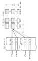
図4には単一セットサイズに該当する2(s+b)バイトのアドレス領域を有するオンチップメモリ140を有し、2(n+s+b)バイトのアドレス領域を有するデータキャッシュ110をテストするのに必要なオンチップメモリ140の類似アドレス領域が表示されている。FIG. 4 shows an on-
図4で2Nセットサイズのアドレス領域を一つセットサイズのアドレス領域を有するオンチップメモリ140にマッピングするためには、類似アドレスデコーダ160が総n+1ビットの類似アドレスビットを持たなければならない。例えば、ARM1020Eデータキャッシュをテストするのに使用されるオンチップメモリ140の大きさが単一セットサイズである512 バイトであれば、64個セットの2倍である128個(すなわち、2(n+1)=27=128)セットサイズのアドレス領域を一つのセットサイズのオンチップメモリ140にマッピングすることができるアドレスデコーディング結果を持たなければならない。In FIG. 4, in order to map the 2N set size address area to the on-
ARM1020Eデータキャッシュの場合、nパラメータの値は6であるので、類似アドレスデコーダ160はn+1に該当する7ビットの類似アドレスビットを考慮しなくアドレスデコーディングを実行する。その結果、図4のように2(n+s+b+1)バイトのアドレス領域を2(s+b)バイトの物理的アドレス領域を有するオンチップメモリ140にマッピングすることができるようになる。この場合、類似アドレスデコーダ160が総n+1ビットの類似アドレスビットを有するので、データキャッシュ110の全体アドレス(full address)がデコーディングされる必要がなく、それによって、デコーディング速度も速くなる。この際、もしタグフィールドのn+1個のビットがデコーディングされない場合にはキャッシュミスが発生するようになる。In the case of the ARM1020E data cache, since the value of the n parameter is 6, the
ここで、データキャッシュ110がNセットサイズのアドレス領域を有するにもかかわらず、オンチップメモリ140が2Nセットサイズの仮想アドレス領域とマッピングされるようにアドレスをデコーディングする理由は、Nセットサイズのアドレスを有してデータキャッシュ110に対するリードミス(read−miss)および書き込みミス(write−miss)に対するテストを実行し、残りのNセットサイズのアドレスを使用してデータキャッシュ110に対するラインフィルおよびキャストアウトに対するテストを実行するためである。これに対する内容は図7および図8を参照して以下詳細に説明する。 Here, the reason why the address is decoded so that the on-
続いて、図5を参照すれば、図5には単一ブロックサイズに該当する2bバイトのアドレス領域を有するオンチップメモリ140を有してデータキャッシュ110をテストするのに必要な類似アドレス領域が表示されている。2(n+s+1)個のブロックサイズのアドレス領域を一つのブロックサイズのアドレス領域にマッピングするためには、類似アドレスデコーダ160が総n+s+1ビットの類似アドレスビットを持たなければならない。Next, referring to FIG. 5, FIG. 5 shows a similar address area necessary for testing the
例えば、ARM1020Eデータキャッシュをテストするのに使用されるオンチップメモリ140の大きさが単一ブロックサイズである32バイトであれば、1024個ブロックの2倍である2048個(すなわち、2(n+s+1)=211=2048)ブロックサイズのアドレス領域を一つのブロックサイズのアドレス領域を有するオンチップメモリ140にマッピングすることができるアドレスデコーディング結果を持たなければならない。ARM1020Eデータキャッシュの場合、nパラメータの値は6であり、sパラメータの値は4であるので、類似アドレスデコーダ160はn+s+1に該当する11ビットのアドレスを考慮しなくアドレスデコーディングを実行する。その結果、図5のように、2bバイトの物理的アドレス領域を有するオンチップメモリ140を有しても2(n+s+b+1)バイトのアドレス領域を有するデータキャッシュ110をテストすることができるようになり、このために、タグフィールドのn+1ビットとセットインデックスのsビットがデコーディングされない時にはキャッシュミスが発生するようになる。For example, if the size of the on-
上述のように、オンチップメモリ140が単一セットサイズに該当する2(s+b)バイトのアドレス領域を有する場合には総n+1ビットの類似アドレスビットを有する一方、オンチップメモリ140が単一ブロックサイズに該当する2bバイトのアドレス領域を有する場合には総n+s+1ビットの類似アドレスビットを有するようになる。すなわち、類似アドレスビットの大きさはオンチップメモリ140の大きさが小くなるほど大きくなり、図5のように、オンチップメモリ140が最小メモリサイズ(すなわち、単一ブロックサイズ)を有する場合の類似アドレスビットの大きさは次のように決められる。As described above, when the on-
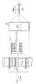
図6は最小メモリサイズのオンチップメモリ140に対する類似アドレス領域の構成を示す図である。図6の(a)にはデータキャッシュ110の全体アドレス領域(full address space)と、データキャッシュ110のサイズ、およびデータキャッシュ110をテストするのに使用されるオンチップメモリ140のサイズが各々示している。そして、図6の(b)にはデータキャッシュ110より小さいサイズのオンチップメモリ140にデータキャッシュ110をテストするのに必要な類似アドレス領域およびデコーディングアドレス領域が示している。 FIG. 6 is a diagram showing a configuration of a similar address area for the on-
図6を参照すれば、類似アドレス領域のサイズADD_SIZESYNONYMとオンチップメモリ140のアドレス領域のサイズADD_SIZEON−CHIPとの和は、式(1)のようにデータキャッシュ110のアドレス領域のサイズADD_SIZED−CACHEより大きく構成されなければならないことが分かる。Referring to FIG. 6, the sum of the size ADD_SIZESYNONYM of the similar address area and the size ADD_SIZEON-CHIP of the address area of the on-
すなわち、本発明でデータキャッシュ110のアドレス領域のサイズADD_SIZED−CACHEは2n+s+bバイトであるので、類似アドレスサイズADD_SIZESYNONYMとオンチップメモリ140のアドレスサイズADD_SIZEON−CHIPの和が2n+s+b+1バイト(ここで、n+s+b+1={n+1+s−x}+x+b以上になるように構成してアドレスをデコーディングする。That is, since the size ADD_SIZED-CACHE of the address area of the
例えば、最小メモリサイズに該当する単一ブロックサイズ(すなわち、32バイト)の大きさを有するオンチップメモリ140を利用してARM1020Eデータキャッシュをテストするためには、1024個ブロックの2倍である2048個(すなわち、2(n+s+1)=211=2048)ブロックサイズのアドレス領域を一つのブロックサイズのアドレス領域を有するオンチップメモリ140にマッピング可能でなければならない。したがって、式1のように、n+s+1に該当する11ビットの類似アドレスビットを有してアドレスデコーディングを実行すれば、図5のように2bバイトの物理的アドレス領域を有するオンチップメモリ140がまるで2(n+s+b+1)バイトのアドレス領域を有するオンチップメモリ140のように動作することができるようになって、小さいサイズのオンチップメモリ140を有しても、これより大きいデータキャッシュ110を十分にテストすることができるようになる。For example, to test the ARM1020E data cache using an on-
図7は本発明の望ましい実施形態によるデータキャッシュ110の実速度テスト方法を概略的に示す図であり、図8は本発明の望ましい実施形態によるデータキャッシュ110の実速度テストの詳細流れ図である。図7および図8には単一セットサイズを有するオンチップメモリ140のための実速度テスト方法が示している。 FIG. 7 is a schematic diagram illustrating a method for testing an actual speed of the
図7および図8を参照すれば、本発明によるデータキャッシュの実速度テスト方法は先にテストを実行する前にデータキャッシュ110をオフさせた後(1100段階)、オンチップメモリ140にテストパターン0(Pattern0)を貯蔵する(1120段階)。そして、データキャッシュ110をオンさせる(1140段階)。次いで、データキャッシュ110にリードミスが発生するようになれば、図7の(a)のように類似アドレス領域に属するデータキャッシュ110のN個のアドレスADD_1〜ADD_N−1を読み込み、これらアドレスが示すオンチップメモリ140の該当のアドレスに貯蔵されているテストパターン0をデータキャッシュ110の該当のアドレス領域に貯蔵するラインフィルを実行する(1200段階)。次いで、リードミスがN回実行されたか否か(すなわち、オンチップメモリ140からテストパターン0を読み込む動作がN回実行されたか否か)を判別する(1250段階)。 Referring to FIGS. 7 and 8, in the data cache actual speed test method according to the present invention, the
1250段階での判別結果、リードミスがN回実行されなければ、該当のキャッシュ110に不良が発生したと判定する。そして、リードミスがN回実行されたら、1200 段階で読み込んだアドレスADD_1〜ADD_N−1を再び読み込む。そして、該当のアドレスにテストパターン0が正しく貯蔵されているか否かを比べて(1300段階)、前記比較結果に基づいてリードヒットがN回発生されたか否かを判別する(1350段階)。 If it is determined in
1350段階での判別結果、リードヒットがN回発生しなければ、該当のキャッシュ110に不良が発生したと判定する。そして、リードヒットがN回発生したら、図7の(b)のように、N個のアドレスADD_1〜ADD_N−1の各々に対して互いに異なる値を有する第1乃至第Nテストパターン(Pattern1〜PatternN)を書き込んだ後、書き込みヒットが発生されたか否かを比べる(1400段階)。ここで、第1乃至第Nテストパターンは互いに異なる値を有するように一定数字を足すか、引くことによって発生されたデータを使用する。 If it is determined in step 1350 that no read hit occurs N times, it is determined that a defect has occurred in the
1400段階での比較結果、書き込みヒットがN回発生しなければ、該当のキャッシュ110に不良が発生したと判定する。そして、書き込みヒットがN回発生したら、図7の(c)および(d)のように前記N個のアドレスADD_1〜ADD_N−1とは異なるアドレス値を有するN個のアドレスADD_N〜ADD_2N−1を読み込んで各アドレス別にラインフィルを実行すると同時にキャストアウトをN回実行する(1500段階)。1500段階でラインフィルおよびキャストアウトに使用されるN個のアドレスADD_N〜ADD_2N−1は先で使用されたN個のアドレスADD_1〜ADD_N−1と同一な類似アドレス領域に属するが(すなわち、先で使用されたN個のアドレスADD_1〜ADD_N−1と同一のオンチップメモリ140のアドレス領域にマッピングされるが)先で使用されたN個のアドレスADD_1〜ADD_N−1とは各々異なるアドレス値を有する。 If a write hit does not occur N times as a result of the comparison in
その結果、オンチップメモリ140に貯蔵されていたテストパターン0はデータキャッシュ110のセット0に満たされるようになり、セット0に貯蔵されていたテストパターン1(Pattern1)はオンチップメモリ140にキャストアウトされる。そして、オンチップメモリ140に貯蔵されていたテストパターン1はデータキャッシュ110のセット1に満たされるようになり、セット1に貯蔵されていたテストパターン2(Pattern2)はオンチップメモリ140にキャストアウトされる。すなわち、データキャッシュ110にリードミスが発生されるごとにテストパターンi−1(Patterni−1)がラインフィルされ、テストパターンi(Patterni)がキャストアウトされる。そして、N個のアドレスADD_N〜ADD_2N−1の各々に対してラインフィルされるテストパターンi−1とキャストアウトされるテストパターンiが一致するか否かが判別される(1550段階)。 As a result, the
1550段階での比較結果、ラインフィルされるテストパターンi−1とキャストアウトされるテストパターンiが互いに一致しなければ、該当のキャッシュ110に不良が発生したと判定する。そして、ラインフィルされるテストパターン i−1とキャストアウトされるテストパターンiが互いに一致すれば、該当のキャッシュ110は正常であると判別する。以上で説明した実速度テスト方法は、テストに使用されたデータキャッシュ110はライトバックキャッシュ(write−back cache)であり、リードミス時、ラインフィルの内容が修正されたダーティーコピー(dirty copy)のキャストアウトより優先し、テストプログラムは命令語キャッシュ(instruction cache)に全部ローディングされているという仮定下で実行される。 If the test pattern i-1 to be line-filled and the test pattern i to be cast out do not coincide with each other as a result of the comparison in
上述のように、本発明によるデータキャッシュの実速度テスト方法はデータキャッシュ110がN個のアドレス領域を有する場合、2N個のアドレス領域をオンチップメモリ140のアドレス領域にデコーディングする。そしてN個のアドレスADD_1〜ADD_N−1を利用してデータキャッシュ110に対するN回のリード−ミス(read−miss)とN回の書き込み−ミス(write−miss)に対するテストを実行し、残りのN個のアドレスADD_N〜ADD_2N−1を利用してデータキャッシュ110に対するラインフィルおよびキャストアウト動作に対するテストを実行する。その結果、データキャッシュ110より小さいサイズを有するオンチップメモリ140を有してもデータキャッシュ110を十分にテストすることができるようになる。 As described above, the data cache actual speed test method according to the present invention decodes 2N address areas into the address area of the on-
以上では、本発明による回路の構成および動作を上述の説明および図に従って示したがこれは例をあげて説明したことに過ぎず、本発明の技術的思想を逸脱しない範囲内で多様な変化および変更が可能であることはもちろんである。 In the above, the configuration and operation of the circuit according to the present invention have been shown according to the above description and the drawings. However, this is merely an example, and various changes and modifications can be made without departing from the technical idea of the present invention. Of course, it can be changed.
本発明はまたコンピュータで読み出すことができる記録媒体にコンピュータが読み出すことができるコードとして実現可能である。コンピュータが読み出す記録媒体はコンピュータシステムによって読み出されることができるデータが貯蔵されるすべての種類の記録装置を含む。コンピュータが読み出すことができる記録媒体の例としてはROM、RAM、CD−ROM、磁気テープ、フロッピー(登録商標)ディスク、光データ貯蔵装置などがあり、またキャリアウエーブ(例えばインターネットを通じた伝送)の形態に実現されることも含む。また、コンピュータが読み出すことができる記録媒体はネットワークで連結されたコンピュータシステムに分散されて、分散方式によってコンピュータが読み出すことができるコードに貯蔵されて実行されることができる。 The present invention can also be implemented as a computer readable code on a computer readable recording medium. Recording media read by a computer include all types of recording devices in which data that can be read by a computer system is stored. Examples of recording media that can be read by a computer include ROM, RAM, CD-ROM, magnetic tape, floppy (registered trademark) disk, optical data storage device, etc., and carrier wave (for example, transmission through the Internet). It is also included to be realized. In addition, a computer-readable recording medium can be distributed in a computer system connected via a network and stored in a code that can be read by the computer in a distributed manner.
100 半導体集積回路
110 データキャッシュ
120 中央処理装置CPU
140 オンチップメモリ
160 類似アドレスデコーダ
100
140 On-
Claims (27)
Translated fromJapanese前記データキャッシュの前記第1データ貯蔵領域より小さい第2データ貯蔵領域を有し、テストデータを貯蔵するオンチップメモリと、
前記オンチップメモリに貯蔵された前記テストデータに対するアクセスが要求されるとき、前記第1データ貯蔵領域が前記第2データ貯蔵領域にマッピングされるようにアドレスをデコーディングするアドレスデコーダとを含むことを特徴とする半導体集積回路。A data cache having a first data storage area;
An on-chip memory having a second data storage area smaller than the first data storage area of the data cache and storing test data;
And an address decoder for decoding an address so that the first data storage area is mapped tothe second data storage area when access to the test data stored in the on-chip memory is requested. A semiconductor integrated circuit.
前記アドレスデコーダは前記ドントケアアドレスビットにn+1ビットを割り当てることを特徴とする請求項3に記載の半導体集積回路。The data cache has 2n sets, each set has 2s blocks, one cache block size is 2b bytes, and the total cache size is 2(s + b + n) bytes, When the on-chip memory has an address area of 2(s + b) bytes corresponding to a single set size,
4. The semiconductor integrated circuit according to claim 3, wherein the address decoder assigns n + 1 bits to the don't care address bits.
前記アドレスデコーダは前記ドントケアアドレスビットにn+s+1ビットを割り当てることを特徴とする請求項3に記載の半導体集積回路。The data cache has 2n sets, each set has 2s blocks, one cache block size is 2b bytes, and the total cache size is 2(s + b + n) bytes, When the on-chip memory has an address area of 2b bytes corresponding to a single block size,
4. The semiconductor integrated circuit according to claim 3, wherein the address decoder assigns n + s + 1 bits to the don't care address bits.
前記半導体集積回路の外部で前記データキャッシュの動作実行の結果を受け入れて前記データキャッシュの欠陥の可否を分析するテスト回路とを含むことを特徴とする半導体集積回路のための実速度テストシステム。An address is decoded such that a data storage area of a data cache is mapped to an on-chip memory having a data storage area smaller than the data cache, and the decoding is performed using test data stored in the on-chip memory. A semiconductor integrated circuit that performs read-miss, write-miss, and line-fill and cast-out operations on the data cache for each address;
An actual speed test system for a semiconductor integrated circuit, comprising: a test circuit that receives a result of execution of the operation of the data cache outside the semiconductor integrated circuit and analyzes whether the data cache is defective or not.
前記データキャッシュの前記N個のアドレスの各々に対して互いに異なる値を有する第2テストデータを書き込み、
前記データキャッシュの前記N個のアドレスとは異なる値を有するN個のアドレスの各々に対して、前記オンチップメモリに貯蔵されている前記第1テストデータを読み出して前記データキャッシュの該当のアドレスに新しい第2テストデータに貯蔵するラインフィルを実行し、前記ラインフィルが実行される間前記データキャッシュの前記アドレスに貯蔵されていた以前の第2テストデータをキャストアウトして前記オンチップメモリに新しい第1テストデータに貯蔵することを特徴とする請求項8に記載の半導体集積回路のための実速度テストシステム。The semiconductor integrated circuit reads the first test data stored in the on-chip memory and performs N line fills on N different addresses of the data cache;
Writing second test data having different values to each of the N addresses of the data cache;
For each of the N addresses having a value different from the N addresses of the data cache, the first test data stored in the on-chip memory is read to the corresponding address of the data cache. A line fill is stored in the new second test data, and the previous second test data stored in the address of the data cache is cast out during the line fill and new to the on-chip memory. 9. The actual speed test system for a semiconductor integrated circuit according to claim 8, wherein the actual test data is stored in the first test data.
(a)前記データキャッシュのアドレス領域を前記データキャッシュより小さい前記オンチップメモリのアドレス領域にデコーディングする段階と、
(b)前記デコーディングされたアドレスに応答して前記オンチップメモリからテストデータを読み出して前記データキャッシュのリード−ミス、書き込み−ミス、ラインフィルおよびキャストアウトをテストする段階とを含むことを特徴とするデータキャッシュの実速度テスト方法。In a method of testing a data cache at an actual speed using an on-chip memory built in a semiconductor integrated circuit,
(A) decoding the address area of the data cache into the address area of the on-chip memory smaller than the data cache;
(B) reading test data from the on-chip memory in response to the decoded address to test read-miss, write-miss, line fill and castout of the data cache. Data cache actual speed test method.
前記ドントケアアドレスビットにn+1ビットが割り当てられることを特徴とする請求項14に記載のデータキャッシュの実速度テスト方法。In the step (a), the data cache has 2n sets, each set has 2s blocks, one cache block size is 2b bytes, and the total cache size is 2When (s + b + n) bytes and the on-chip memory has an address area of 2(s + b) bytes corresponding to a single set size,
The method of claim 14, wherein n + 1 bits are assigned to the don't care address bits.
前記ドントケアアドレスビットにn+s+1ビットが割り当てられることを特徴とする請求項14に記載のデータキャッシュの実速度テスト方法。In the step (a), the data cache has 2n sets, each set has 2s blocks, one cache block size is 2b bytes, and the total cache size is 2When (s + b + n) bytes and the on-chip memory has a 2b byte address area corresponding to a single block size,
The method according to claim 14, wherein n + s + 1 bits are assigned to the don't care address bits.
(b−1)前記オンチップメモリに貯蔵されている第1テストデータを読み出して前記データキャッシュのN個の互いに異なるアドレスに対してN回のラインフィルを実行して前記ラインフィル動作の欠陥の可否を判別する段階と、
(b−2)前記データキャッシュの前記N個のアドレスの各々に対して互いに異なる値を有する第2テストデータを書き込んで前記書き込み動作の欠陥の可否を判別する段階と、
(b−3)前記データキャッシュの前記N個のアドレスとは異なる値を有するN個のアドレスの各々に対して、前記オンチップメモリに貯蔵されている前記第1テストデータを読み出して前記データキャッシュの該当のアドレスに新しい第2テストデータに貯蔵するラインフィルを実行し、前記ラインフィルが実行される間前記データキャッシュの前記アドレスに貯蔵されていた以前の第2テストデータをキャストアウトして前記オンチップメモリに新しい第1テストデータに貯蔵して、前記ラインフィルおよびキャストアウト動作の欠陥の可否を判別する段階とを含むことを特徴とする請求項12に記載のデータキャッシュの実速度テスト方法。The step (b) includes (b-1) reading the first test data stored in the on-chip memory, executing N line fills on N different addresses of the data cache, and Determining whether or not a line fill operation is defective;
(B-2) writing second test data having different values to each of the N addresses of the data cache to determine whether or not the writing operation is defective;
(B-3) Reading the first test data stored in the on-chip memory for each of the N addresses having a value different from the N addresses of the data cache to read the data cache A line fill to store new second test data at the corresponding address, and cast out the previous second test data stored at the address of the data cache during the line fill. 13. The method according to claim 12, further comprising: storing new first test data in an on-chip memory to determine whether the line fill and cast-out operation is defective. .
前記(b−1)段階の以前に
(b−1−1)前記データキャッシュをオフする段階と、
(b−1−2)前記オンチップメモリに前記第1テストデータを貯蔵する段階と、
(b−1−3)前記データキャッシュをオンする段階とをさらに含むことを特徴とする請求項19に記載のデータキャッシュの実速度テスト方法。The actual speed test method is:
(B-1-1) turning off the data cache before the step (b-1);
(B-1-2) storing the first test data in the on-chip memory;
20. The data cache actual speed test method according to claim 19, further comprising: (b-1-3) turning on the data cache.
(a)前記データキャッシュのアドレス領域を前記データキャッシュより小さい前記オンチップメモリのアドレス領域にデコーディングする段階と、
(b)前記デコーディングされたアドレスに応答して前記オンチップメモリからテストデータを読み出して前記データキャッシュに対するリード−ミス、書き込み−ミス、ラインフィルおよびキャストアウト動作を実行し、前記実行結果を前記半導体集積回路の外部のテスト装置に出力する段階と、
(c)前記テスト装置で前記データキャッシュの動作実行の結果を分析して、前記データキャッシュの欠陥の可否を判断する段階とを含むことを特徴とする半導体集積回路のための実速度テスト方法。In a method of testing a data cache at an actual speed using an on-chip memory built in a semiconductor integrated circuit,
(A) decoding the address area of the data cache into the address area of the on-chip memory smaller than the data cache;
(B) Reading test data from the on-chip memory in response to the decoded address to perform read-miss, write-miss, line fill and cast-out operations on the data cache, Outputting to a test device outside the semiconductor integrated circuit;
(C) analyzing the result of execution of the operation of the data cache by the test device, and determining whether the data cache is defective or not. A real speed test method for a semiconductor integrated circuit, comprising:
(b−1)前記オンチップメモリに貯蔵されている第1テストデータを読み出して前記データキャッシュのN個の互いに異なるアドレスに対してN回のラインフィルを実行する段階と、
(b−2)前記データキャッシュの前記N個のアドレスの各々に対して互いに異なる値を有する第2テストデータを書き込む段階と、
(b−3)前記データキャッシュの前記N個のアドレスとは異なる値を有するN個のアドレスの各々に対して、前記オンチップメモリに貯蔵されている前記第1テストデータを読み出して前記データキャッシュの該当のアドレスに新しい第2テストデータに貯蔵するラインフィルを実行し、前記ラインフィルが実行される間前記データキャッシュの前記アドレスに貯蔵されていた以前の第2テストデータをキャストアウトして前記オンチップメモリに新しい第1テストデータに貯蔵する段階とを含むことを特徴とする請求項23に記載の半導体集積回路のための実速度テスト方法。In step (b),
(B-1) reading the first test data stored in the on-chip memory and performing N line fills on N different addresses of the data cache;
(B-2) writing second test data having different values to each of the N addresses of the data cache;
(B-3) Reading the first test data stored in the on-chip memory for each of the N addresses having a value different from the N addresses of the data cache to read the data cache A line fill to store new second test data at the corresponding address, and cast out the previous second test data stored at the address of the data cache during the line fill. 24. The method of claim 23, further comprising: storing new first test data in an on-chip memory.
Applications Claiming Priority (2)
| Application Number | Priority Date | Filing Date | Title |
|---|---|---|---|
| KR2004-043646 | 2004-06-14 | ||
| KR1020040043646AKR101014413B1 (en) | 2004-06-14 | 2004-06-14 | Semiconductor integrated circuit with data cache and its at-speed-test method |
Publications (2)
| Publication Number | Publication Date |
|---|---|
| JP2006004419A JP2006004419A (en) | 2006-01-05 |
| JP4833586B2true JP4833586B2 (en) | 2011-12-07 |
Family
ID=35460344
Family Applications (1)
| Application Number | Title | Priority Date | Filing Date |
|---|---|---|---|
| JP2005162840AExpired - Fee RelatedJP4833586B2 (en) | 2004-06-14 | 2005-06-02 | Semiconductor integrated circuit with built-in data cache and its actual speed test method |
Country Status (3)
| Country | Link |
|---|---|
| US (1) | US7173839B2 (en) |
| JP (1) | JP4833586B2 (en) |
| KR (1) | KR101014413B1 (en) |
Families Citing this family (5)
| Publication number | Priority date | Publication date | Assignee | Title |
|---|---|---|---|---|
| US7564380B2 (en)* | 2007-08-02 | 2009-07-21 | General Electric Company | Systems and methods for storing test data and accessing test data |
| US9037928B2 (en)* | 2012-01-01 | 2015-05-19 | Mosys, Inc. | Memory device with background built-in self-testing and background built-in self-repair |
| CN104412327B (en)* | 2013-01-02 | 2019-02-12 | 默思股份有限公司 | Built-in self-test and repair device and method |
| CN103440186B (en)* | 2013-07-22 | 2017-02-22 | 记忆科技(深圳)有限公司 | Method and system for testing cache acceleration |
| US10176099B2 (en)* | 2016-07-11 | 2019-01-08 | Intel Corporation | Using data pattern to mark cache lines as invalid |
Family Cites Families (16)
| Publication number | Priority date | Publication date | Assignee | Title |
|---|---|---|---|---|
| US4167782A (en)* | 1977-12-22 | 1979-09-11 | Honeywell Information Systems Inc. | Continuous updating of cache store |
| US4575792A (en) | 1982-03-31 | 1986-03-11 | Honeywell Information Systems Inc. | Shared interface apparatus for testing the memory sections of a cache unit |
| JP3139818B2 (en) | 1992-03-30 | 2001-03-05 | 日本碍子株式会社 | Verification method of accuracy in moisture determination of solids |
| JPH05342104A (en)* | 1992-06-12 | 1993-12-24 | Fujitsu Ltd | How to diagnose cache memory |
| JPH0689199A (en)* | 1992-09-09 | 1994-03-29 | Fujitsu Ltd | Cache function diagnosis method |
| JPH0764863A (en)* | 1993-08-30 | 1995-03-10 | Nec Shizuoka Ltd | Automatic discrimination system for cache memory |
| US6199142B1 (en) | 1996-07-01 | 2001-03-06 | Sun Microsystems, Inc. | Processor/memory device with integrated CPU, main memory, and full width cache and associated method |
| US5974579A (en)* | 1996-09-03 | 1999-10-26 | Credence Systems Corporation | Efficient built-in self test for embedded memories with differing address spaces |
| US5805606A (en)* | 1997-03-13 | 1998-09-08 | International Business Machines Corporation | Cache module fault isolation techniques |
| JPH1139228A (en)* | 1997-07-15 | 1999-02-12 | Pfu Ltd | Diagnosis method for cache memory replacement control mechanism, diagnosis apparatus therefor, and recording medium |
| US6161206A (en) | 1998-04-30 | 2000-12-12 | Credence Systems Corporation | Pattern generator for a semiconductor integrated circuit tester |
| US6748558B1 (en)* | 2000-05-10 | 2004-06-08 | Motorola, Inc. | Performance monitor system and method suitable for use in an integrated circuit |
| JP2002367395A (en)* | 2001-06-04 | 2002-12-20 | Fujitsu Ltd | TAG-RAM test method and apparatus therefor |
| JP2003139818A (en)* | 2001-10-30 | 2003-05-14 | Hitachi Ltd | Semiconductor integrated circuit and method of testing semiconductor integrated circuit |
| US7269766B2 (en) | 2001-12-26 | 2007-09-11 | Arm Limited | Method and apparatus for memory self testing |
| JP2005309787A (en)* | 2004-04-21 | 2005-11-04 | Nec Electronics Corp | Central processing unit and microcomputer |
- 2004
- 2004-06-14KRKR1020040043646Apatent/KR101014413B1/ennot_activeExpired - Fee Related
- 2005
- 2005-03-31USUS11/096,137patent/US7173839B2/ennot_activeExpired - Fee Related
- 2005-06-02JPJP2005162840Apatent/JP4833586B2/ennot_activeExpired - Fee Related
Also Published As
| Publication number | Publication date |
|---|---|
| US7173839B2 (en) | 2007-02-06 |
| KR101014413B1 (en) | 2011-02-15 |
| JP2006004419A (en) | 2006-01-05 |
| KR20050118515A (en) | 2005-12-19 |
| US20050276087A1 (en) | 2005-12-15 |
Similar Documents
| Publication | Publication Date | Title |
|---|---|---|
| CN101292228B (en) | Lock indicator for conversion lookaside buffer | |
| KR100372293B1 (en) | Cacheable Properties for Virtual Addresses in Virtual and Physical Index Caches | |
| US8230179B2 (en) | Administering non-cacheable memory load instructions | |
| Shirvani et al. | PADded cache: a new fault-tolerance technique for cache memories | |
| US6848024B1 (en) | Programmably disabling one or more cache entries | |
| JP4218820B2 (en) | Cache system including direct mapped cache and full associative buffer, its control method and recording medium | |
| US7979669B1 (en) | Method and system for caching attribute data for matching attributes with physical addresses | |
| US20060117129A1 (en) | High speed DRAM cache architecture | |
| US7831774B2 (en) | Pipelining D states for MRU steerage during MRU-LRU member allocation | |
| US7222217B2 (en) | Cache residency test instruction | |
| US6226763B1 (en) | Method and apparatus for performing cache accesses | |
| JP4669244B2 (en) | Cache memory device and memory control method | |
| US20020087825A1 (en) | Error detection in cache tag array using valid vector | |
| JP4833586B2 (en) | Semiconductor integrated circuit with built-in data cache and its actual speed test method | |
| US7343455B2 (en) | Cache mechanism and method for avoiding cast out on bad victim select and recycling victim select operation | |
| US7302530B2 (en) | Method of updating cache state information where stores only read the cache state information upon entering the queue | |
| US7987320B2 (en) | Cache mechanism and method for avoiding cast out on bad victim select and recycling victim select operation | |
| US20060143397A1 (en) | Dirty line hint array for cache flushing | |
| US6968427B1 (en) | Built-in self test circuit for testing cache tag array and compare logic | |
| CN100451994C (en) | Microprocessor, apparatus and method for selectively associating store buffer cache line status with response buffer cache line status | |
| KR100833178B1 (en) | Cache memory system and method for controlling the number of blocks stored in cache memory | |
| KR20040047398A (en) | Method for data access using cache memory | |
| US12032479B2 (en) | Metadata-caching integrated circuit device | |
| WO2025186533A1 (en) | Tag-non-preserving write operation | |
| US7624224B1 (en) | System and method for directly executing code from block-based memory |
Legal Events
| Date | Code | Title | Description |
|---|---|---|---|
| A621 | Written request for application examination | Free format text:JAPANESE INTERMEDIATE CODE: A621 Effective date:20080528 | |
| A131 | Notification of reasons for refusal | Free format text:JAPANESE INTERMEDIATE CODE: A131 Effective date:20110531 | |
| A521 | Request for written amendment filed | Free format text:JAPANESE INTERMEDIATE CODE: A523 Effective date:20110729 | |
| TRDD | Decision of grant or rejection written | ||
| A01 | Written decision to grant a patent or to grant a registration (utility model) | Free format text:JAPANESE INTERMEDIATE CODE: A01 Effective date:20110823 | |
| A01 | Written decision to grant a patent or to grant a registration (utility model) | Free format text:JAPANESE INTERMEDIATE CODE: A01 | |
| A61 | First payment of annual fees (during grant procedure) | Free format text:JAPANESE INTERMEDIATE CODE: A61 Effective date:20110922 | |
| R150 | Certificate of patent or registration of utility model | Free format text:JAPANESE INTERMEDIATE CODE: R150 | |
| FPAY | Renewal fee payment (event date is renewal date of database) | Free format text:PAYMENT UNTIL: 20140930 Year of fee payment:3 | |
| LAPS | Cancellation because of no payment of annual fees |