JP4830256B2 - Display device, display device drive circuit, and display device drive method - Google Patents
Display device, display device drive circuit, and display device drive methodDownload PDFInfo
- Publication number
- JP4830256B2 JP4830256B2JP2003428890AJP2003428890AJP4830256B2JP 4830256 B2JP4830256 B2JP 4830256B2JP 2003428890 AJP2003428890 AJP 2003428890AJP 2003428890 AJP2003428890 AJP 2003428890AJP 4830256 B2JP4830256 B2JP 4830256B2
- Authority
- JP
- Japan
- Prior art keywords
- source
- transistor
- voltage
- signal
- signal level
- Prior art date
- Legal status (The legal status is an assumption and is not a legal conclusion. Google has not performed a legal analysis and makes no representation as to the accuracy of the status listed.)
- Expired - Fee Related
Links
Images


Classifications
- G—PHYSICS
- G09—EDUCATION; CRYPTOGRAPHY; DISPLAY; ADVERTISING; SEALS
- G09G—ARRANGEMENTS OR CIRCUITS FOR CONTROL OF INDICATING DEVICES USING STATIC MEANS TO PRESENT VARIABLE INFORMATION
- G09G2310/00—Command of the display device
- G09G2310/02—Addressing, scanning or driving the display screen or processing steps related thereto
- G09G2310/0243—Details of the generation of driving signals
- G09G2310/0254—Control of polarity reversal in general, other than for liquid crystal displays
- G09G2310/0256—Control of polarity reversal in general, other than for liquid crystal displays with the purpose of reversing the voltage across a light emitting or modulating element within a pixel
Landscapes
- Control Of El Displays (AREA)
- Electroluminescent Light Sources (AREA)
- Control Of Indicators Other Than Cathode Ray Tubes (AREA)
Description
Translated fromJapanese本発明は、ディスプレイ装置、ディスプレイ装置の駆動回路及びディスプレイ装置の駆動方法に関し、例えば有機EL(Electro Luminescence)素子によるディスプレイ装置に適用することができる。本発明は、ソースフォロワ回路構成のトランジスタにより発光素子を電流駆動する場合に、信号線の信号レベルによりゲートソース間に設けた信号レベル保持用のコンデンサの端子電圧を設定して、この信号レベル保持用のコンデンサの端子間電圧によるゲートソース間電圧により発光素子を駆動するようにして、このトランジスタのソース側端を基準電圧に接続してこの基準電圧により階調を低下させるように信号レベル保持用のコンデンサに設定される端子間電圧をオフセットさせることにより、ソースフォロワ回路構成によるトランジスタにより発光素子を駆動する構成において、面ザラ、黒浮き、コントラストの劣化を防止する。 The present invention relates to a display device, a display device drive circuit, and a display device drive method, and can be applied to, for example, a display device using an organic EL (Electro Luminescence) element. The present invention maintains the signal level by setting the terminal voltage of the signal level holding capacitor provided between the gate and the source according to the signal level of the signal line when the light emitting element is driven by a transistor having a source follower circuit configuration. For maintaining the signal level, the light emitting element is driven by the voltage between the gate and the source due to the voltage between the terminals of the capacitor, and the source side end of this transistor is connected to the reference voltage, and the gradation is lowered by this reference voltage. By offsetting the inter-terminal voltage set in the capacitor, the surface roughness, black floating, and contrast deterioration are prevented in the configuration in which the light emitting element is driven by the transistor having the source follower circuit configuration.
従来、有機ELの表示装置においては、例えばUSP5,684,365、特開平8−234683号公報等にディスプレイ装置への応用が種々に提案されるようになされている。 Conventionally, in organic EL display devices, various applications to display devices have been proposed, for example, in US Pat. No. 5,684,365 and JP-A-8-234683.
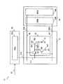
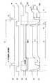
すなわち図12に示すように、この種のディスプレイ装置1において、画素部2は、マトリックス状に配置されてなる画素(PX)3に対して、走査線SCNがライン単位で水平方向に設けられ、またこの走査線SCNと直交するように信号線SIGが各列毎に垂直方向に設けられる。このようにして形成されてなる画素部2に対して、ディスプレイ装置1は、垂直駆動回路4により走査線SCNを駆動して順次ライン単位で画素部2の画素3を駆動すると共に、この画素3の駆動に対応するように水平駆動回路5により信号線SIGを駆動して各画素3の階調を設定するようになされている。 That is, as shown in FIG. 12, in this type of
このため垂直駆動回路4は、ライトスキャン回路(WSCN)4Aにより、各画素3への書き込みをライン単位で順次指示する書き込み信号wsを生成し、この書き込み信号wsを走査線SCNに出力して各画素3における階調の設定を制御するようになされている。また水平駆動回路5は、各画素3の階調を指示する階調データD1に応じて駆動信号を生成し、この駆動信号を水平セレクタ(HSEL)5Aにより各信号線SIGに振り分けて出力し、これらによりディスプレイ装置1は、ライン単位で各画素3の階調を設定するようになされている。 For this reason, the
有機ELのディスプレイ装置においては、このようにして駆動される各画素3が、電流駆動による自発光型の素子である有機EL素子と、この有機EL素子を駆動する各画素の駆動回路(以下、画素回路と呼ぶ)とにより形成されるようになされている。 In the organic EL display device, each
しかしてこのようにして形成されるディスプレイ装置においては、nチャンネルMOS型のTFT(Thin Film Transistor)により各画素回路を形成することにより、また有機EL素子のアノードをトランジスタに接続してこのトランジスタにより電流駆動することにより、アモルファスシリコンのプロセスを適用して有機EL素子と画素回路とをガラス基板上に一体に形成することができ、これにより図13に示すように、ソースフォロワ回路構成により有機EL素子12を駆動することが考えられる。 In the display device thus formed, each pixel circuit is formed by an n-channel MOS type TFT (Thin Film Transistor), and the anode of the organic EL element is connected to the transistor. By driving with current, an organic EL element and a pixel circuit can be integrally formed on a glass substrate by applying an amorphous silicon process. As a result, as shown in FIG. It is conceivable to drive the
すなわちこの図14に示すディスプレイ装置11は、各画素3において、有機EL素子12のアノードにソースを接続してなるソースフォロワ回路構成のトランジスタTR2により有機EL素子12を電流駆動するように形成され、このトランジスタTR2のゲートに信号レベル保持用のコンデンサC1が設けられる。ディスプレイ装置11は、垂直駆動回路4に設けたライトスキャン回路4Aから書き込み信号wsを出力するようにして、この書き込み信号wsによりオン動作するトランジスタTR1によるスイッチ回路により、この信号レベル保持用のコンデンサC1が信号線SIGに接続され、これにより書き込み信号wsに応動して信号線SIGに出力される駆動信号の信号レベルによりトランジスタTR2のゲート電圧Vgが設定される。これによりこのディスプレイ装置11は、このように設定されたゲート電圧Vgに応じた電流により有機EL素子12を駆動し、階調データD1に応じた階調により各画素3の有機EL素子12を発光させて所望の画像を表示できるようになされている。 That is, the
しかしながら有機EL素子においては、図14に示すように、使用により電流が流れ難くなる方向に電流電圧特性が変化する。なおこの図14及び図15において、符号L1が初期の特性を示し、符号L2が経時変化による特性を示すものである。これに対して図13について上述したソーフフォロワ回路による駆動においては、図15に示すように、トランジスタTR2のドレインソース間電圧Vds−ドレインソース電流Idsの特性曲線に対して、負荷による特性曲線が交差してなる交点が動作点となる。これにより有機EL素子において、電圧電流特性が変化すると、その分、有機EL素子に流れる電流が減少し、これらにより各画素の輝度が徐々に低下する問題がある。 However, in an organic EL element, as shown in FIG. 14, the current-voltage characteristics change in a direction in which current hardly flows through use. In FIG. 14 and FIG. 15, the symbol L1 indicates the initial characteristics, and the symbol L2 indicates the characteristics due to changes over time. On the other hand, in the driving by the sofa follower circuit described above with reference to FIG. 13, the characteristic curve due to the load intersects the characteristic curve of drain-source voltage Vds−drain source current Ids of the transistor TR2, as shown in FIG. The intersecting point becomes the operating point. Accordingly, in the organic EL element, when the voltage-current characteristic is changed, the current flowing through the organic EL element is reduced correspondingly, thereby causing a problem that the luminance of each pixel is gradually lowered.
この問題を解決する1つの方法として、ゲートソース間電圧Vgsによる階調の設定により有機EL素子12の駆動電流を制御する方法が考えられる。すなわちTFTのドレイン電流Idsにおいては、(1/2)×μ×(W/L)Cox(Vgs−Vth)2 ……(1)により表され、これによりゲートソース間電圧Vgsによる階調の設定により経時変化による駆動電流の変化を防止することができる。ここでμはキャリアの移動度、Wはゲート幅、Lはゲート長、Coxは単位面積当たりのゲート容量、Vthはしきい値電圧である。As one method for solving this problem, a method of controlling the drive current of the
これにより図13との対比により図16に示すように、各画素23において、トランジスタTR2のゲートドレインに対する信号レベル保持用のコンデンサC1の配置に代えて、このトランジスタTR2のゲートソース間に信号レベル保持用のコンデンサC2を配置し、この信号レベル保持用のコンデンサC2に信号線SIGの信号レベルを設定する。またドライブスキャン信号ds1によりオン動作するトランジスタTR3をトランジスタTR2のソースに接続し、信号レベル保持用のコンデンサC2に信号線SIGの信号レベルを設定する期間の間、このトランジスタTR3によりトランジスタTR2のソース電位を一定電位に設定すると共に、有機EL素子12の発光を停止する。なお図16においては、この一定電位がアース電位の場合である。 Accordingly, as shown in FIG. 16 in comparison with FIG. 13, in each
またこのような画素23による画素部22の構成に対応して、垂直駆動回路24においては、ライトスキャン回路24Aに加えて、このライトスキャン回路24Aによる書き込み信号wsの出力に同期してドライブスキャン信号ds1を出力するドライブスキャン回路(DSCN)24Bを設け、また水平駆動回路25においては、駆動信号を生成して水平セレクタ25Aより出力する。 Corresponding to the configuration of the
しかして実際上、図17(A)〜(D)及び図18(A)〜(D)に示すように、これによりこのディスプレイ装置21では、ドライブスキャン信号ds1によるトランジスタTR3のオンオフ動作により有機EL素子12の発光、非発光を制御する。またトランジスタTR3のオン制御によりトランジスタTR2のソース電位を一定電位に設定して有機EL素子12の発光を停止している期間で、書き込み信号wsによりトランジスタTR1をオン動作させ、信号レベル保持用のコンデンサC2に信号線SIGの信号レベルVinを設定する。またその後、書き込み信号wsを立ち下げてトランジスタTR1をオフ状態に設定した後、ドライブスキャン信号ds1を立ち下げ、これによりソース電圧Vsが立ち上がって信号レベル保持用のコンデンサC2に設定された信号レベルVinに応じた電流駆動により有機EL素子12を駆動する。なお図18(A)〜(D)は、図17の各期間TA〜TDにそれぞれ対応するトランジスタTR2、TR3の設定を示す接続図である。 Accordingly, in practice, as shown in FIGS. 17A to 17D and FIGS. 18A to 18D, the
このようにしてゲートドレイン間電圧Vgdによる階調の設定に代えてゲートソース間電圧による階調の設定により有機EL素子12の駆動電流を制御すれば、有機EL素子12の特性が変化した場合であっても、階調データにより決まる一定電流により駆動し得、これにより経時変化による画質の劣化等を有効に回避することができる。 In this way, when the drive current of the
しかしながら上述した(1)式により判るように、このようにして有機EL素子12による経時変化を防止するようにしても、トランジスタTR2のしきい値電圧Vthがばらついた場合には、その分、各画素23における駆動電流がばらつくようになり、これにより画質が劣化する。このようなトランジスタTR2のしきい値電圧Vthのばらつきによる画質劣化を防止する方法として、信号レベル保持用のコンデンサC2に信号線SIGの信号レベルを設定する際に、事前に、トランジスタTR2のしきい値電圧Vthをこの信号レベル保持用のコンデンサC2にセットする方法が考えられる。 However, as can be seen from the above-described expression (1), even when the change with time due to the
すなわちこの場合図16との対比により図19に示すように、トランジスタTR2のゲートソース間に設ける信号レベル保持用のコンデンサCs2に対して、カップリング用のコンデンサCs1を介してトランジスタTR1により信号線SIGの信号レベルを設定するようにして、トランジスタTR2のゲートソース間を短絡させてトランジスタTR2をダイオード接続に切り換えるトランジスタTR5によるスイッチ回路、カップリング用のコンデンサCs1のトランジスタTR1側端を基準電位に設定するトランジスタTR6によるスイッチ回路を設ける。これによりこのディスプレイ装置31では、トランジスタTR1によりコンデンサCs1を介して信号線SIGの信号レベルVinにより信号レベル保持用のコンデンサCs2の端子電圧を設定する。この場合、カップリング用のコンデンサCs1を介した信号線SIGへの接続により、信号レベル保持用のコンデンサCs2の端子間電圧は、信号線SIGの信号レベルVinをコンデンサCs1、Cs2により分圧した電圧ΔVin=Vin(Cs1/(Cs1+Cs2))……(2)だけ上昇することになる。これによりこの関係式を考慮して、水平駆動回路35により信号線SIGが駆動される。 That is, in this case, as shown in FIG. 19 in comparison with FIG. 16, the signal line SIG is connected to the signal level holding capacitor Cs2 provided between the gate and source of the transistor TR2 by the transistor TR1 via the coupling capacitor Cs1. Is set so that the gate side of the transistor TR2 is short-circuited to switch the transistor TR2 to the diode connection, and the transistor TR1 side end of the coupling capacitor Cs1 is set to the reference potential. A switch circuit by the transistor TR6 is provided. Thereby, in this display device 31, the terminal voltage of the signal level holding capacitor Cs2 is set by the signal level Vin of the signal line SIG via the capacitor Cs1 by the transistor TR1. In this case, due to the connection to the signal line SIG via the coupling capacitor Cs1, the voltage between the terminals of the signal level holding capacitor Cs2 is a voltage obtained by dividing the signal level Vin of the signal line SIG by the capacitors Cs1 and Cs2. ΔVin = Vin (Cs1 / (Cs1 + Cs2))... (2). Accordingly, the signal line SIG is driven by the
これにより図20及び図21に示すように、この場合も、画素33においては、信号レベル保持用のコンデンサCs2に設定された電圧によるゲートソース間電圧VgsによりトランジスタTR2で有機EL素子12を駆動して、有機EL素子12の経時変化による画質劣化が防止される(図20(D)〜(F)及び図21(A))。 As a result, as shown in FIGS. 20 and 21, in this case as well, in the
このように信号線SIGの信号レベルVinにより信号レベル保持用のコンデンサCs2の端子電圧を設定する直前で、このディスプレイ装置31は、制御信号azによりトランジスタTR5をオン状態に設定してトランジスタTR2をダイオード接続すると共に、カップリング用のコンデンサCs1の信号線側端を所定の基準電位に保持し(図20(B)及び図21(B))、その後、ドライブスキャン信号ds1、ds2の切り換えにより、トランジスタTR2のソースを基準電位に設定すると共に、トランジスタTR2への電源の供給を停止する(図20(C)、(D)及び図21(C))。 Thus, immediately before the terminal voltage of the capacitor Cs2 for holding the signal level is set by the signal level Vin of the signal line SIG, the display device 31 sets the transistor TR5 to the ON state by the control signal az and makes the transistor TR2 a diode. At the same time, the signal line side end of the coupling capacitor Cs1 is held at a predetermined reference potential (FIG. 20B and FIG. 21B), and then the drive scan signals ds1 and ds2 are switched, whereby the transistor The source of TR2 is set to the reference potential, and the supply of power to the transistor TR2 is stopped (FIGS. 20C, 20D, and 21C).
これらによりトランジスタTR2においては、一時的に立ち上がったゲート電圧Vgが徐々に低下し、ゲートソース間電圧Vgsがしきい値電圧Vthになると、ゲート電圧Vgの低下が停止し、これにより信号レベル保持用のコンデンサCs2にトランジスタTR2のしきい値電圧Vthが設定される(図20(E)及び(F))。 As a result, in the transistor TR2, the gate voltage Vg that has risen temporarily decreases gradually, and when the gate-source voltage Vgs reaches the threshold voltage Vth, the decrease in the gate voltage Vg is stopped, thereby maintaining the signal level. The threshold voltage Vth of the transistor TR2 is set in the capacitor Cs2 (FIGS. 20E and 20F).
これにより制御信号azを切り換えてカップリング用コンデンサCs1の信号線側端を基準電圧より切り離すと共に、トランジスタTR2のダイオード接続を中止した後、書き込み信号wsを立ち上げ、カップリング用のコンデンサCs1を介して信号線SIGの信号レベルVinにより信号レベル保持用のコンデンサCs2の端子電圧を設定する。これにより信号レベル保持用のコンデンサCs2においては、トランジスタTR2のしきい値電圧Vthにより補正されて信号線SIGの信号レベルに対応する電圧が設定され、トランジスタTR2においては、このコンデンサCs2に設定された電圧によるゲートソース間電圧Vgsにより有機EL素子12を電流駆動し(図21(E))、トランジスタTR2のしきい値電圧Vthによるばらつきを防止することができる。 As a result, the control signal az is switched to disconnect the signal line side end of the coupling capacitor Cs1 from the reference voltage, and after the diode connection of the transistor TR2 is stopped, the write signal ws is raised and passed through the coupling capacitor Cs1. Thus, the terminal voltage of the signal level holding capacitor Cs2 is set by the signal level Vin of the signal line SIG. As a result, the signal level holding capacitor Cs2 is corrected by the threshold voltage Vth of the transistor TR2, and a voltage corresponding to the signal level of the signal line SIG is set. In the transistor TR2, the capacitor Cs2 is set. The
これらの画素33の構成に対応して、ディスプレイ装置31においては、垂直駆動回路34に、書き込み信号wsを出力するライトスキャン回路34A、ドライブスキャン信号ds1、ドライブスキャン信号ds2をそれぞれ出力するドライブスキャン回路24B、24Cを設け、さらにしきい値電圧Vthの補正に係るトランジスタTR5、TR6の制御信号azを出力するオートゼロ回路(ZERO)34Dを設けるようにする。また水平駆動回路35においては、水平セレクタ35Aより各信号線SIGに駆動信号を出力する。 Corresponding to the configuration of these
このようにすれば、有機EL素子12を駆動するトランジスタTR2のしきい値電圧Vthがばらついた場合にあっても、このばらつきによる画質の劣化を防止することができる。 In this way, even when the threshold voltage Vth of the transistor TR2 that drives the
ところで図16について上述したディスプレイ装置21のようにして、信号レベル保持用のコンデンサC2の端子電圧の設定により有機EL素子12の階調を設定する場合、黒階調においては、信号線SIGの信号レベルVinは0〔V〕に設定され、その結果、信号レベル保持用のコンデンサC2の端子間電圧にあってもトランジスタTR2のしきい値電圧以下の0〔V〕に保持される。これにより本来ならば、トランジスタTR2のカットオフにより有機EL素子12に何ら電流が供給されないようになり、これにより有機EL素子12においては、何ら発光しないことになる。 When the gradation of the
しかしながらトランジスタTR2の特性がディプリーションの場合、しきい値電圧Vthは、0〔V〕より低い電圧となる。これによりこの場合は、信号線SIGの信号レベルを0〔V〕に設定して信号レベル保持用のコンデンサC2の端子電圧を設定しても、トランジスタTR2に電流が流れ、これにより有機EL素子12が黒の階調で発光することになる。これにより図16に示す構成によるディスプレイ装置21においては、例えば全面を黒階調に設定した場合、微小に発光する画素が発生し、表示画面がザラついたように見て取られるいわゆる面ザラが発生する問題があった。またこのように本来黒レベルによる表示において、有機EL素子12が僅かながらではあるが発光することにより、黒レベルによる階調が白レベル側に浮き上がったように見て取られるいわゆる黒浮きが発生する問題があり、さらには黒レベル側においてコントラストが低下する問題があった。 However, when the characteristic of the transistor TR2 is depletion, the threshold voltage Vth is lower than 0 [V]. Accordingly, in this case, even if the signal level of the signal line SIG is set to 0 [V] and the terminal voltage of the signal level holding capacitor C2 is set, a current flows through the transistor TR2, thereby the
これに対して図19に示す構成のディスプレイ装置31においては、事前に、信号レベル保持用のコンデンサCs2にトランジスタTR2のしきい値電圧Vthを設定することにより、このようなディプリーションの特性による面ザラ、黒浮き、コントラストの低下については解消することができる。 On the other hand, in the display device 31 having the configuration shown in FIG. 19, the threshold voltage Vth of the transistor TR2 is set in advance in the signal level holding capacitor Cs2, thereby obtaining such depletion characteristics. Surface roughness, black float, and contrast reduction can be eliminated.
しかしながら信号レベル保持用のコンデンサCs2へのしきい値電圧Vthの設定においては、ばらつきを避け得ず、また有機EL素子を駆動するトランジスタTR2自体もばらつくことになる。これによりこのようにしてトランジスタTR2のしきい値電圧Vthを補正する場合、(1)式について上述した括弧内の−Vthの項を完全にキャンセルし得ず、僅かながらではあるが、信号レベル保持用のコンデンサCs2に設定される電圧にばらつきが発生する。 However, in setting the threshold voltage Vth to the signal level holding capacitor Cs2, variation cannot be avoided, and the transistor TR2 itself for driving the organic EL element also varies. As a result, when the threshold voltage Vth of the transistor TR2 is corrected in this way, the term of -Vth in the parentheses described above with respect to the expression (1) cannot be completely canceled, and the signal level is maintained slightly. Variation occurs in the voltage set in the capacitor Cs2.
このようなばらつきにあっては、信号レベル保持用のコンデンサCs2に設定する本来の電圧が高い場合にあっては、殆ど問題とならないのに対し、信号レベル保持用のコンデンサCs2に設定する電圧が低い場合、本来の端子間電圧に対して相対的にばらつきの電圧が大きくなることにより、表示画像に影響を与えることになる。これにより図19に示す構成によるディスプレイ装置31においても、面ザラ、黒浮きが発生し、コントラストが低下する問題があった。
本発明は以上の点を考慮してなされたもので、ソースフォロワ回路構成によるトランジスタにより発光素子を駆動する構成において、面ザラ、黒浮き、コントラストの劣化を防止することができるディスプレイ装置、ディスプレイ装置の駆動回路及びディスプレイ装置の駆動方法を提案しようとするものである。 The present invention has been made in consideration of the above points. In a configuration in which a light emitting element is driven by a transistor having a source follower circuit configuration, a display device and a display device capable of preventing surface roughness, black floating, and contrast deterioration can be prevented. A drive circuit and a display device drive method are proposed.
かかる課題を解決するため、本願発明においては、電流駆動による画素をマトリックス状に配置してなる画素部と、画素部を駆動する駆動回路とを有するディスプレイ装置に適用して、画素は、発光素子と、ゲートソース間に信号レベル保持用のコンデンサを保持し、信号レベル保持用のコンデンサの端子間電圧によるゲートソース間電圧により発光素子を駆動するソースフォロワ回路によるトランジスタと、トランジスタのゲートを信号線に接続する信号線用のスイッチ回路と、トランジスタのソースをソース側の基準電圧に接続するソース側のスイッチ回路とを有し、駆動回路は、ソース側のスイッチ回路をオン状態に設定して、トランジスタのソース電位をソース側の基準電圧に設定した状態で、信号線のスイッチ回路の駆動により、信号線の信号レベルにより信号レベル保持用のコンデンサの端子電圧を設定することにより、発光素子の駆動に供するトランジスタのゲートソース間電圧を設定し、ソース側の基準電圧が、信号線の信号レベルにより設定される信号レベル保持用のコンデンサの端子間電圧を、階調が低下する側にオフセットさせる電圧であり、前記駆動回路は、黒レベル以外の階調において、前記黒レベルの階調に対応する各階調の信号レベルを、前記ソース側の基準電圧の分、階調を増大させる側にオフセットさせて前記信号線の駆動信号を生成するようにする。In order to solve this problem, the present invention is applied to a display device having a pixel portion in which pixels driven by current drive are arranged in a matrix and a drive circuit for driving the pixel portion. And a transistor with a source follower circuit that holds a signal level holding capacitor between the gate and source and drives the light emitting element by a gate-source voltage by a voltage between terminals of the signal level holding capacitor, and a gate of the transistor as a signal line. A switch circuit for a signal line connected to the source circuit, and a switch circuit on the source side for connecting the source of the transistor to a reference voltage on the source side, and the drive circuit sets the switch circuit on the source side to an on state, With the source potential of the transistor set to the reference voltage on the source side, by driving the switch circuit of the signal line, By setting the terminal voltage of the capacitor for holding the signal level according to the signal level of the signal line, the voltage between the gate and source of the transistor used to drive the light emitting element is set, and the reference voltage on the source side is set by the signal level of the signal line the terminal voltage of the capacitor for signal level holding that is,Ri voltage der to offset the side where the gradation isreduced, wherein the driving circuit in the tone other than black level, corresponding to the gradation of the black level A signal for driving the signal line is generated by offsetting the signal level of each gradation to the side where the gradation is increased by the reference voltage on the source side .
また、電流駆動による画素をマトリックス状に配置してなるディスプレイ装置に適用して、画素は、発光素子と、ゲートソース間に信号レベル保持用のコンデンサを保持し、信号レベル保持用のコンデンサの端子間電圧によるゲートソース間電圧により発光素子を駆動するソースフォロワ回路によるトランジスタと、一定の期間、トランジスタのゲートを信号線に接続し、信号レベル保持用のコンデンサの端子電圧を信号線の信号レベルにより設定する信号線用のスイッチ回路と、少なくとも信号線用のスイッチ回路によりトランジスタのゲートを信号線に接続している期間の間、トランジスタのソースをソース側の基準電圧に接続するソース側のスイッチ回路とを有し、ソース側の基準電圧が、信号線の信号レベルにより設定される信号レベル保持用のコンデンサの端子間電圧を、階調が低下する側にオフセットさせる電圧であるようにする。In addition, the pixel is applied to a display device in which pixels driven by current are arranged in a matrix, and the pixel holds a signal level holding capacitor between the light emitting element and the gate source, and the signal level holding capacitor terminal A transistor with a source follower circuit that drives a light-emitting element by a gate-source voltage by an inter-voltage, and a gate of the transistor is connected to a signal line for a certain period, and the terminal voltage of a capacitor for holding a signal level depends on the signal level of the signal line The switch circuit for the signal line to be set and the switch circuit on the source side for connecting the source of the transistor to the reference voltage on the source side during at least the period when the gate of the transistor is connected to the signal line by the switch circuit for the signal line The reference voltage on the source side is set to the signal level set by the signal level of the signal line. The terminal voltage of the capacitor for Le holding gradation is to be a voltage that is offset to the side to decrease.
また、有機EL素子による画素をマトリックス状に配置してなるディスプレイ装置に適用して、画素は、有機EL素子と、ゲートソース間に信号レベル保持用のコンデンサを保持し、信号レベル保持用のコンデンサの端子間電圧によるゲートソース間電圧により有機EL素子を駆動するソースフォロワ回路によるトランジスタと、一定の期間、トランジスタのゲートを信号線に接続し、信号レベル保持用のコンデンサの端子電圧を信号線の信号レベルにより設定する信号線用のスイッチ回路と、少なくとも信号線用のスイッチ回路によりトランジスタのゲートを信号線に接続している期間の間、トランジスタのソースをソース側の基準電圧に接続するソース側のスイッチ回路とを有し、ソース側の基準電圧が、信号線の信号レベルにより設定される信号レベル保持用のコンデンサの端子間電圧を、階調が低下する側にオフセットさせる電圧であるようにする。Further, a pixel of an organic EL device applied to a display apparatus formed by arranging in a matrix, the pixel holds the organic EL element, a capacitor for signal level held in between the gate and the source, a capacitor for signal level holding The transistor of the source follower circuit that drives the organic EL element by the gate-source voltage by the voltage between the terminals of the transistor and the gate of the transistor is connected to the signal line for a certain period, and the terminal voltage of the signal level holding capacitor is A switch circuit for a signal line that is set according to a signal level, and a source side that connects the source of the transistor to a reference voltage on the source side at least during a period in which the gate of the transistor is connected to the signal line by the switch circuit for the signal line The reference voltage on the source side is set according to the signal level of the signal line. The terminal voltage of the capacitor for signal level holding that gradation is to be a voltage that is offset to the side to decrease.
また、電流駆動による画素をマトリックス状に配置してなるディスプレイ装置の駆動回路に適用して、画素は、発光素子と、ゲートソース間に信号レベル保持用のコンデンサを保持し、信号レベル保持用のコンデンサの端子間電圧によるゲートソース間電圧により発光素子を駆動するソースフォロワ回路によるトランジスタと、一定の期間、トランジスタのゲートを信号線に接続し、信号レベル保持用のコンデンサの端子電圧を信号線の信号レベルにより設定する信号線用のスイッチ回路と、少なくとも信号線用のスイッチ回路によりトランジスタのゲートを信号線に接続している期間の間、トランジスタのソースをソース側の基準電圧に接続するソース側のスイッチ回路とを有し、ソース側の基準電圧が、信号線の信号レベルにより設定される信号レベル保持用のコンデンサの端子間電圧を、階調が低下する側にオフセットさせる電圧であり、ディスプレイ装置の駆動回路は、黒レベル以外の階調において、黒レベルの階調に対応する各階調の信号レベルを、ソース側の基準電圧の分、階調を増大させる側にオフセットさせて信号線の駆動信号を生成する。In addition, the pixel is applied to a driving circuit of a display device in which pixels driven by current are arranged in a matrix, and the pixel holds a capacitor for holding a signal level between the light emitting element and the gate source, and holds the signal level. A transistor with a source follower circuit that drives a light emitting element by a gate-source voltage by a voltage between terminals of a capacitor and a gate of the transistor is connected to a signal line for a certain period, and a terminal voltage of a capacitor for holding a signal level is A switch circuit for a signal line that is set according to a signal level, and a source side that connects the source of the transistor to a reference voltage on the source side at least during a period in which the gate of the transistor is connected to the signal line by the switch circuit for the signal line The reference voltage on the source side is set according to the signal level of the signal line. The voltage across the terminals of the capacitor for holding the signal level is offset to the side where the gray level is lowered, and the drive circuit of the display device has a gray level other than the black level corresponding to the black level gray level. The signal level drive signal is generated by offsetting the tone signal level to the side of increasing the gradation by the reference voltage on thesource side.
また、電流駆動による画素をマトリックス状に配置してなる画素部と、画素部を駆動する駆動回路とを有するディスプレイ装置の駆動方法に適用して、画素は、発光素子と、ゲートソース間に信号レベル保持用のコンデンサを保持し、信号レベル保持用のコンデンサの端子間電圧によるゲートソース間電圧により発光素子を駆動するソースフォロワ回路によるトランジスタと、トランジスタのゲートを信号線に接続する信号線用のスイッチ回路と、トランジスタのソースをソース側の基準電圧に接続するソース側のスイッチ回路とを有し、ディスプレイ装置の駆動方法は、ソース側のスイッチ回路をオン状態に設定して、トランジスタのソース電位をソース側の基準電圧に設定した状態で、信号線用のスイッチ回路の駆動により、信号線の信号レベルにより信号レベル保持用のコンデンサの端子電圧を設定することにより、発光素子の駆動に供するトランジスタのゲートソース間電圧を設定し、ソース側の基準電圧が、信号線の信号レベルにより設定される信号レベル保持用のコンデンサの端子間電圧を、階調が低下する側にオフセットさせる電圧であり、前記駆動方法は、黒レベル以外の階調において、前記黒レベルの階調に対応する各階調の信号レベルを、前記ソース側の基準電圧の分、階調を増大させる側にオフセットさせて前記信号線の駆動信号を生成するようにする。In addition, when applied to a driving method of a display device having a pixel portion in which pixels driven by current drive are arranged in a matrix and a driving circuit for driving the pixel portion, the pixel has a signal between a light emitting element and a gate source. A transistor with a source follower circuit that holds a level holding capacitor and drives a light emitting element by a gate-source voltage by a voltage between terminals of the signal level holding capacitor, and a signal line for connecting the gate of the transistor to the signal line And a source-side switch circuit for connecting a source of the transistor to a reference voltage on the source side. The driving method of the display device sets the source-side switch circuit to an ON state, and sets the source potential of the transistor Is set to the reference voltage on the source side, and the signal line signal is driven by driving the switch circuit for the signal line. By setting the terminal voltage of the capacitor for holding the signal level according to the level, the gate-source voltage of the transistor used for driving the light emitting element is set, and the reference voltage on the source side is set by the signal level of the signal line the terminal voltage of the capacitor for level holding,Ri voltage der to offset the side where the gradation isreduced, the driving method, the gradation other than the black level, the gradation corresponding to the gradation of the black level The signal level is offset to the side where the gray level is increased by an amount corresponding to the reference voltage on the source side to generate the drive signal for the signal line .
本願発明の構成により、電流駆動による画素をマトリックス状に配置してなる画素部と、画素部を駆動する駆動回路とを有するディスプレイ装置に適用して、画素は、発光素子と、ゲートソース間に信号レベル保持用のコンデンサを保持し、信号レベル保持用のコンデンサの端子間電圧によるゲートソース間電圧により発光素子を駆動するソースフォロワ回路によるトランジスタと、トランジスタのゲートを信号線に接続する信号線用のスイッチ回路と、トランジスタのソースをソース側の基準電圧に接続するソース側のスイッチ回路とを有し、駆動回路は、ソース側のスイッチ回路をオン状態に設定して、トランジスタのソース電位をソース側の基準電圧に設定した状態で、信号線のスイッチ回路の駆動により、信号線の信号レベルにより信号レベル保持用のコンデンサの端子電圧を設定することにより、発光素子の駆動に供するトランジスタのゲートソース間電圧を設定すれば、信号線の信号レベルにより信号レベル保持用のコンデンサの端子電圧を設定した後、この信号レベル保持用のコンデンサの端子間電圧によるゲートソース間電圧によりトランジスタで発光素子を電流駆動し得、これにより発光素子の経時変化による影響を有効に回避して、発光素子を駆動することができる。このときこのような信号線の信号レベルにより信号レベル保持用のコンデンサの端子電圧を設定する際に、ソース側に接続されるソース側の基準電圧が、信号線の信号レベルにより設定される信号レベル保持用のコンデンサの端子間電圧を、階調が低下する側にオフセットさせる電圧であることにより、単にコンデンサ側の基準電圧を設定するだけで、黒レベルで確実に発光素子を発光させないようにすることができ、これにより発光素子を駆動するトランジスタのしきい値電圧を補正するようにして、面ザラ、黒浮き、コントラストの劣化を防止することができる。According to the configuration of thepresent invention , the pixel is applied between a light emitting element and a gate source when applied to a display device having a pixel portion in which pixels driven by current drive are arranged in a matrix and a driving circuit for driving the pixel portion. A transistor with a source follower circuit that holds a signal level holding capacitor and drives a light emitting element by a gate-source voltage by a voltage between terminals of the signal level holding capacitor, and a signal line that connects the gate of the transistor to the signal line And a source-side switch circuit for connecting the source of the transistor to a reference voltage on the source side, and the drive circuit sets the source-side switch circuit to an on state so that the source potential of the transistor is sourced With the reference voltage on the side set, by driving the signal line switch circuit, depending on the signal level of the signal line By setting the terminal voltage of the capacitor for holding the signal level, the terminal voltage of the capacitor for holding the signal level is set according to the signal level of the signal line if the gate-source voltage of the transistor used for driving the light emitting element is set. Thereafter, the light-emitting element can be current-driven by the transistor by the voltage between the gate and the source due to the voltage between the terminals of the signal level holding capacitor, thereby effectively avoiding the influence of the light-emitting element over time and driving the light-emitting element. be able to. At this time, when setting the terminal voltage of the signal level holding capacitor according to the signal level of such a signal line, the reference voltage on the source side connected to the source side is set to the signal level set by the signal level of the signal line. Since the voltage between the terminals of the holding capacitor is offset to the gradation-decreasing side, it is ensured that the light emitting element does not emit light at the black level by simply setting the reference voltage on the capacitor side. Thus, by correcting the threshold voltage of the transistor that drives the light emitting element, surface roughness, black floating, and deterioration of contrast can be prevented.
また、電流駆動による画素、有機EL素子による画素をマトリックス状に配置してなるディスプレイ装置に適用して、面ザラ、黒浮き、コントラストの劣化を防止することができる。また、面ザラ、黒浮き、コントラストの劣化を防止することができるディスプレイ装置の駆動回路を提供することができる。また、発光素子を駆動するトランジスタのしきい値電圧を補正するようにしてなるディスプレイ装置について、面ザラ、黒浮き、コントラストの劣化を防止することができるディスプレイ装置の駆動方法を提供することができる。Further, by applying the pixel of the current driver, the pixel with an organic EL device to a display apparatus formed by arranging in a matrix, the surface Zara, black float,Ru can be prevented from deterioration ofcontrast. Further, it is possible to provide a display device driving circuit capable of preventing surface roughness, black floating, and contrast deterioration. In addition, for a display device configured to correct the threshold voltage of a transistor that drives a light emitting element, it is possible to provide a display device driving method that can prevent surface roughness, black floating, and contrast deterioration. .
本発明によれば、ソースフォロワ回路構成により発光素子をトランジスタにより駆動する構成において、面ザラ、黒浮き、コントラストの劣化を防止することができる。 According to the present invention, in a configuration in which a light emitting element is driven by a transistor with a source follower circuit configuration, surface roughness, black floating, and contrast deterioration can be prevented.
以下、適宜図面を参照しながら本発明の実施例を詳述する。 Hereinafter, embodiments of the present invention will be described in detail with reference to the drawings as appropriate.
(1)実施例の構成
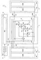
図1は、図16との対比により本発明の実施例1に係るディスプレイ装置を示す接続図である。このディスプレイ装置51において、画素部52は、電流駆動による画素53がマトリックス状に配置され、これらの画素53に対して、走査線SCN、SCN1がライン単位で水平方向に設けられる。またこれらの走査線SCN、SCN1と直交するように信号線SIGが各列毎に垂直方向に設けられる。このようにして形成されてなる画素部52に対して、ディスプレイ装置51は、垂直駆動回路54により走査線SCN、SCN1を駆動して順次ライン単位で画素53に設けられた画素回路の動作を制御すると共に、この画素回路の制御に対応するように水平駆動回路55により信号線SIGを駆動して各画素53の階調を設定するようになされている。(1) Configuration of Embodiment FIG. 1 is a connection diagram showing a display device according to
このため垂直駆動回路54は、各画素53への書き込みをライン単位で順次指示する書き込み信号wsをライトスキャン回路(WSCN)54Aにより生成し、またこの書き込み信号wsに同期してドライブスキャン信号ds1をドライブスキャン回路54Bにより生成し、これら書き込み信号ws、ドライブスキャン信号ds1を走査線SCN、SCN1に出力して各画素53における階調の設定を制御するようになされている。また水平駆動回路55においては、各画素53の階調を指示する階調データD1に応じて駆動信号を生成し、この駆動信号を水平セレクタ(HSEL)55Aにより各信号線SIGに振り分けて出力するようになされている。 Therefore, the
このディスプレイ装置51に係る画素53においては、トランジスタTR2のソースをトランジスタTR3により基準電圧Vofに接続するようになされ、この基準電圧Vofが、信号レベル保持用のコンデンサC2への信号線SIGの信号レベルの設定において、負のオフセット電圧を与える電源に設定されるようになされている。各画素53においては、このトランジスタTR3に係る基準電圧Vofの設定が異なる点を除いて、図16のディスプレイ装置21の画素13と同一に構成される。 In the
具体的に、基準電圧Vofは、電源Vcc側に所定電位だけ立ち上がる正側電源電圧に設定される。また電圧値にあっては、トランジスタTR2のしきい値電圧Vthが種々にばらついた場合でも、このしきい値電圧Vthを越える電圧に設定され、これによりディスプレイ装置41では、黒レベルの階調により信号レベル保持用のコンデンサC2の端子電圧を設定して、トランジスタTR2を確実にカットオフさせることができるようになされている。このためこの実施例では、この画素部52に各種の電源を供給する電源回路において、この基準電圧Vofを調整できるように形成され、この調整により、基準電圧Vofが、黒レベルの階調によっては各画素53が発光しない電圧に設定されるようになされている。 Specifically, the reference voltage Vof is set to a positive power supply voltage that rises by a predetermined potential on the power supply Vcc side. In addition, the voltage value is set to a voltage exceeding the threshold voltage Vth even when the threshold voltage Vth of the transistor TR2 varies. The terminal voltage of the signal level holding capacitor C2 is set so that the transistor TR2 can be surely cut off. For this reason, in this embodiment, the power supply circuit for supplying various power supplies to the
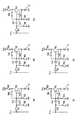
これによりこの画素53においては、図2に示すように、黒レベルによる階調の設定においては、確実にトランジスタTR2をカットオフさせて有機EL素子12を駆動しないようにして、面ザラ、黒浮き、コントラストの低下を防止するようになされている。なおこの図2は、黒レベルにより階調を表示する場合の例である。 As a result, in the
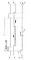
すなわちこの場合、図2に示すように、この画素53においては、信号レベル保持用のコンデンサC2に保持された端子間電圧によるゲートソース間電圧Vgsにより有機EL素子12を駆動して、ドライブスキャン信号ds1により発光、非発光が制御される(図2(B)〜(D))。ディスプレイ装置51では、このドライブスキャン信号ds1による非発光の設定により、トランジスタTR2のソース電圧が基準電圧Vofに保持され、またこのようにしてトランジスタTR2のソース電圧を基準電圧Vofに保持した状態で、この非発光の一部期間で書き込み信号wsが立ち上げられ(図2(A))、これによりトランジスタTR1によりトランジスタTR2のゲートが信号線SIGに接続され、信号レベル保持用のコンデンサC2の端子電圧が信号線SIGの信号レベルVinに設定される。 That is, in this case, as shown in FIG. 2, in this
しかしてこの場合、信号レベル保持用のコンデンサC2の他端においては、トランジスタTR2のソースに接続されて、基準電圧Vofに保持されていることにより、結局、信号レベル保持用のコンデンサC2においては、この信号線SIGの信号レベルVinによる端子電圧の設定により、端子間電圧がVin−Vofに設定され、これにより階調が低下する側に基準電圧Vofにより信号線SIGの信号レベルVinがオフセットされて設定される。 In this case, the other end of the signal level holding capacitor C2 is connected to the source of the transistor TR2 and held at the reference voltage Vof. By setting the terminal voltage based on the signal level Vin of the signal line SIG, the inter-terminal voltage is set to Vin−Vof, whereby the signal level Vin of the signal line SIG is offset by the reference voltage Vof to the side where the gradation is lowered. Is set.
これにより画素53においては、トランジスタTR2の特性がディプリーションの場合でも、黒レベルの階調については、トランジスタTR2のゲートソース間電圧VgsをトランジスタTR2のしきい値電圧以下に設定して、確実に有機EL素子12を発光させないようにし得、これにより面ザラ、黒浮き、コントラストの劣化を防止することができるようになされている。 Thus, in the
(2)実施例の動作
以上の構成において、このディスプレイ装置51は(図2)、垂直駆動回路54による走査線SCN、SCN1の駆動により順次ライン単位で水平駆動回路55により駆動される信号線SIGの信号レベルが各画素53に設定される。ディスプレイ装置51は、この各画素53に設定した信号レベルにより各画素53が発光して所望の画像が表示される。(2) Operation of Embodiment In the above configuration, the display device 51 (FIG. 2) is configured such that the signal line SIG driven by the horizontal drive circuit 55 sequentially in units of lines by driving the scanning lines SCN and SCN1 by the
ディスプレイ装置51では、各画素53において、有機EL素子12を駆動するソースフォロワ回路構成のトランジスタTR2のゲートソース間に信号レベル保持用のコンデンサC2が設けられ、トランジスタTR1によるスイッチ回路によりこのトランジスタTR2のゲートを信号線SIGに接続することにより、信号レベル保持用のコンデンサC2の端子電圧が信号線SIGの信号レベルVinに設定される。またこのようにして設定した信号レベル保持用のコンデンサC2の端子間電圧によるゲートソース間電圧VgsによりトランジスタTR2で有機EL素子12が電流駆動される。 In the
これによりディスプレイ装置51においては、有機EL素子12の電圧電流特性の経時変化による駆動電流の変化を防止し得、有機EL素子12の経時変化による画質の劣化を有効に回避することができる。また各画素53をnチャンネル型MOSトランジスタにより形成し、またトランジスタTR2によるアノード側より有機EL素子12を駆動することができ、これらによりアモルファスシリコンのプロセスを適用して有機EL素子と画素回路とをガラス基板上に一体に形成することができる。 As a result, in the
ディスプレイ装置51では、このような信号線SIGの信号レベルVinによる信号レベル保持用のコンデンサC2の端子電圧の設定において、トランジスタTR2のソースがトランジスタTR3により基準電圧Vofに設定され、これにより信号レベル保持用のコンデンサC2においては、他端側が基準電圧Vofに保持された状態で、信号線SIGの信号レベルVinにより一端の端子電圧が設定され、端子間電圧がVin−Vofに設定される。これにより信号レベル保持用のコンデンサC2においては、階調を低下させるように、端子間電圧がこの基準電圧Vofの分だけ低い電圧にオフセットされて設定される。 In the
この実施例では、トランジスタTR2の特性がディプリーションの場合でも、黒レベルの階調については、確実にトランジスタTR2のカットオフさせることができる電圧にこのオフセットさせる基準電圧Vofが設定されていることにより、ディスプレイ装置51では、この基準電圧Vofを設定するだけの簡易な構成により、黒レベルの階調については、有機EL素子12を発光させない電圧に設定され、これにより面ザラ、黒浮き、コントラストの劣化を防止することができる。 In this embodiment, even when the characteristic of the transistor TR2 is depletion, for the black level gradation, the reference voltage Vof to be offset to the voltage that can surely cut off the transistor TR2 is set. Therefore, in the
(3)実施例の効果
以上の構成によれば、ソースフォロワ回路構成のトランジスタにより発光素子を電流駆動する場合に、信号線の信号レベルによりゲートソース間に設けた信号レベル保持用のコンデンサの端子電圧を設定して、この信号レベル保持用のコンデンサの端子間電圧によるゲートソース間電圧により発光素子を駆動するようにして、このトランジスタのソース側端を基準電圧に接続してこの基準電圧により階調を低下させるように信号レベル保持用のコンデンサに設定される端子間電圧をオフセットさせることにより、ソースフォロワ回路構成によるトランジスタにより発光素子を駆動する構成において、簡易な構成により面ザラ、黒浮き、コントラストの劣化を防止することができる。(3) Effects of the embodiment According to the above configuration, when the light emitting element is driven by the transistor having the source follower circuit configuration, the terminal of the signal level holding capacitor provided between the gate and the source according to the signal level of the signal line. The voltage is set, and the light emitting element is driven by the voltage between the gate and the source due to the voltage between the terminals of the signal level holding capacitor. The source side end of the transistor is connected to the reference voltage, and the reference voltage is used to adjust the level. By offsetting the inter-terminal voltage set in the signal level holding capacitor so as to lower the tone, the structure in which the light emitting element is driven by the transistor by the source follower circuit configuration, the surface roughness, black floating, Degradation of contrast can be prevented.
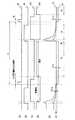
図3は、図1との対比により本発明の実施例2に係るディスプレイ装置を示す接続図である。このディスプレイ装置61においては、トランジスタTR2のドレインと電源Vccとの間にトランジスタTR4によるスイッチ回路が設けられ、このスイッチ回路によりトランジスタTR2への電源の供給を制御する。なおこのディスプレイ装置61においては、このトランジスタTR4に関連する構成が異なる点を除いて、実施例1のディスプレイ装置51と同一に構成される。これによりこのディスプレイ装置61では、垂直駆動回路64に、書き込み信号wsを出力するライトスキャン回路64A、ドライブスキャン信号ds1を出力するドライブスキャン回路64Bが設けられ、またさらにトランジスタTR4の制御に係るドライブスキャン信号ds2を出力するドライブスキャン回路64Cが設けられるようになされている。また水平駆動回路65は、階調データD1に応じて駆動信号を生成し、この駆動信号を水平セレクタ65Aにより出力するようになされている。 FIG. 3 is a connection diagram showing a display apparatus according to the second embodiment of the present invention in comparison with FIG. In this
ここで図4に示すように、このディスプレイ装置61では、トランジスタTR3に代えて、トランジスタTR4の制御により有機EL素子12の発光、非発光を制御し、これにより非発光の期間においては、各画素回路で電力を消費しないようにし、全体の消費電力を軽減する。 As shown in FIG. 4, in this
またこのようにして発光、非発光を制御して、非発光の期間の所定のタイミングで書き込み信号wsを立ち上げて信号線SIGの信号レベルVinにより信号レベル保持用のコンデンサC2の端子電圧を設定する。またこのように信号レベル保持用のコンデンサC2の端子電圧を信号線SIGの信号レベルVinにより設定する期間においては、トランジスタTR3をオン状態に設定し、信号レベル保持用のコンデンサC2の他端の電圧を基準電圧Vofに保持する。 In addition, by controlling light emission and non-light emission in this way, the write signal ws is raised at a predetermined timing in the non-light emission period, and the terminal voltage of the signal level holding capacitor C2 is set by the signal level Vin of the signal line SIG. To do. In this way, in the period in which the terminal voltage of the signal level holding capacitor C2 is set by the signal level Vin of the signal line SIG, the transistor TR3 is set to the on state, and the voltage at the other end of the signal level holding capacitor C2 is set. Is maintained at the reference voltage Vof.
これによりこの実施例においても、トランジスタのソース側端を基準電圧に接続してこの基準電圧により階調を低下させるように信号レベル保持用のコンデンサに設定される端子間電圧をオフセットさせるようになされている。 As a result, also in this embodiment, the source-side end of the transistor is connected to the reference voltage, and the voltage between the terminals set in the signal level holding capacitor is offset so that the gradation is lowered by this reference voltage. ing.
図3の構成によれば、電源Vccに設けたトランジスタTR4によるスイッチ回路によりトランジスタTR2への電源の供給を制御して発光、非発光を制御するようにしても、実施例1と同様の効果を得ることができる。 According to the configuration of FIG. 3, even if the supply of power to the transistor TR2 is controlled by the switch circuit by the transistor TR4 provided in the power supply Vcc to control light emission and non-light emission, the same effect as in the first embodiment can be obtained. Obtainable.
図5は、図19との対比により本発明の実施例2に係るディスプレイ装置を示す接続図である。このディスプレイ装置71においては、図19について上述したディスプレイ装置31と同様に、トランジスタTR4により有機EL素子12の発光、非発光を制御し、非発光の期間の間で、トランジスタTR5、TR6をオン状態に設定して信号レベル保持用のコンデンサCs2にトランジスタTR2のしきい値電圧Vthを設定した後、トランジスタTR1によりこの信号レベル保持用のコンデンサCs2の端子電圧を信号線SIGの信号レベルVinにより設定する。これによりこの実施例においては、有機EL素子12の経時変化、トランジスタTR2のしきい値電圧Vthのばらつきによる画質劣化を防止するようになされている。 FIG. 5 is a connection diagram showing a display apparatus according to the second embodiment of the present invention in comparison with FIG. In the
このため画素部72の各画素73においては、カップリング用のコンデンサCs1、トランジスタTR5、TR6によるしきい値電圧Vthの補正に係る構成が設けられ、また垂直駆動回路74においては、書き込み信号ws、ドライブスキャン信号ds1、ds2をそれぞれ出力するライトスキャン回路74A、ドライブスキャン回路74B、74Dが設けられ、またトランジスタTR5、TR6の制御に係る制御信号azを出力するオートゼロ回路74Dが設けられるようになされている。 Therefore, each
図20及び図21との対比により図6及び図7に示すように、このディスプレイ装置71では、このように信号レベル保持用のコンデンサCs2にトランジスタTR2のしきい値電圧Vthを設定した後、トランジスタTR1によりこの信号レベル保持用のコンデンサCs2の端子電圧を信号線SIGの信号レベルVinにより設定する際に、信号レベル保持用のコンデンサCs2の他端がトランジスタTR3により基準電圧Vofに接続される。これによりこの実施例においても、この基準電圧Vofにより、信号線SIGの信号レベルVinにより設定される信号レベル保持用のコンデンサCs2の端子間電圧を、階調が低下する側にオフセットさせるようになされている。なお図20は、黒レベルの階調により有機EL素子12を駆動する場合である。 As shown in FIGS. 6 and 7 in comparison with FIGS. 20 and 21, in this
具体的に、基準電圧Vofは、電源Vcc側に所定電位だけ立ち上がる正側電源電圧に設定される。また電圧値にあっては、信号レベル保持用のコンデンサCs2にトランジスタTR2のしきい値電圧Vthを設定して、このしきい値電圧Vthの設定、トランジスタTR2がばらついた場合でも、黒レベルの階調により信号レベル保持用のコンデンサCs2を設定して、トランジスタTR2を確実にカットオフさせる電圧を信号レベル保持用のコンデンサCs2に設定する電圧に設定される。このためこの実施例では、この画素部52に各種の電源を供給する電源回路において、この基準電圧Vofを調整できるように形成される。 Specifically, the reference voltage Vof is set to a positive power supply voltage that rises by a predetermined potential on the power supply Vcc side. As for the voltage value, the threshold voltage Vth of the transistor TR2 is set in the signal level holding capacitor Cs2, and even if the threshold voltage Vth is set and the transistor TR2 varies, the black level is reduced. The capacitor Cs2 for holding the signal level is set by adjustment, and the voltage for surely cutting off the transistor TR2 is set to the voltage for setting the capacitor Cs2 for holding the signal level. For this reason, in this embodiment, the power supply circuit for supplying various power supplies to the
これによりこの画素73においては、黒レベルによる階調の設定においては、確実にトランジスタTR2をカットオフさせて有機EL素子12を駆動しないようにして、面ザラ、黒浮き、コントラストの低下を防止するようになされている。 Thus, in this
このような画素73における基準電圧Vofによるオフセット電圧の供給に対応して、このディスプレイ装置71において、シグナルドライバ75Bは、階調データD1により指示される階調に対して、図8及び図9に示すような特性により駆動信号を生成して信号線に出力する。ここで図8は、信号レベル保持用のコンデンサCs2の端子間電圧Vcs2と階調データD1による階調を示す特性曲線図であり、図9は、信号線SIGに出力する駆動信号の信号レベルVinと階調データD1との関係を示す特性曲線図である。また符号L3は、トランジスタTR3によりトランジスタTR2のソースをアース電位に接続する場合の特性曲線であり、符号L4は、この実施例に係る特性曲線である。 Corresponding to the supply of the offset voltage by the reference voltage Vof in the
通常、この種のディスプレイ装置の駆動信号は、有機EL素子12の発光特性に対応して、階調の増大により順次信号レベルが0レベルから増大するように設定され(図8、符号L3)、これによりトランジスタTR3によりトランジスタTR2のソースをアース電位に接続して黒レベルの階調を表示する場合、信号レベル保持用のコンデンサCs2の端子間電圧Vcs2は、トランジスタTR2のしきい値電圧Vthに設定され(図8、符号L3)、これによりトランジスタTR2においては、本来、カットオフ状態に保持されて有機EL素子12を駆動し得ず、黒レベルの階調が表現されることになる。 Usually, the drive signal of this type of display device is set so that the signal level sequentially increases from 0 level as the gray level increases corresponding to the light emission characteristics of the organic EL element 12 (FIG. 8, reference L3). As a result, when the transistor TR3 connects the source of the transistor TR2 to the ground potential to display a black level gradation, the voltage Vcs2 between the terminals of the signal level holding capacitor Cs2 is set to the threshold voltage Vth of the transistor TR2. As a result, the transistor TR2 is originally held in the cut-off state and cannot drive the
しかしながらこの実施例においては、基準電圧Vofにより信号レベル保持用のコンデンサCs2に設定される端子間電圧をオフセットさせることにより、トランジスタTR3によりトランジスタTR2のソースをアース電位に接続する場合と同様の特性により駆動信号を生成した場合には、黒側に階調が沈み込んで階調を正しく表現することが困難になり、また黒レベルに続く階調において、黒レベルの階調における場合の面ザラ等の問題が発生することになる。 However, in this embodiment, by offsetting the voltage between terminals set in the signal level holding capacitor Cs2 by the reference voltage Vof, the transistor TR3 has the same characteristics as when the source of the transistor TR2 is connected to the ground potential. When the drive signal is generated, the gradation sinks on the black side, making it difficult to correctly express the gradation, and in the gradation following the black level, surface roughness in the case of the black level gradation, etc. Will cause problems.
このためシグナルドライバ75Bは、黒レベルについては、トランジスタTR3によりトランジスタTR2のソースをアース電位に接続する場合と同一の信号レベルにより駆動信号を生成する。また黒レベル以外については、トランジスタTR3によりトランジスタTR2のソースをアース電位に接続する場合に対して、基準電圧Vofに対応する分だけ高い電圧により駆動信号を生成する。なおこの基準電圧Vofに対応する分だけの高い電圧にあっては、カップリング用のコンデンサCs1を介して信号レベル保持用のコンデンサCs1の端子電圧を設定することによる(2)式について上述した関係式による電圧である。これによりこの実施例では、黒レベル以外の階調において、黒レベルの階調に対応する各階調の信号レベルを、ソース側の基準電圧Vofの分、階調を増大させる側にオフセットさせて信号線SIGの駆動信号を生成するようになされ、これにより信号レベル保持用のコンデンサCs2の端子間電圧をオフセットさせて面ザラ等を防止するようにして、正しい階調により画像表示できるようになされている。 For this reason, the
この実施例によれば、トランジスタTR2のしきい値電圧を信号レベル保持用のコンデンサCs2に設定した後、信号線の信号レベルにより信号レベル保持用のコンデンサCs2の端子電圧を設定する構成においても、このトランジスタのソース側端を基準電圧に接続してこの基準電圧により階調を低下させるように信号レベル保持用のコンデンサに設定される端子間電圧をオフセットさせることにより、面ザラ、黒浮き、コントラストの劣化を防止することができる。 According to this embodiment, after setting the threshold voltage of the transistor TR2 to the signal level holding capacitor Cs2, the terminal voltage of the signal level holding capacitor Cs2 is set according to the signal level of the signal line. By connecting the source side end of this transistor to a reference voltage and offsetting the voltage between terminals set in the signal level holding capacitor so that the gradation is lowered by this reference voltage, surface roughness, black floating, contrast Can be prevented.
図10は、本発明の実施例4に係るディスプレイ装置を示す接続図である。このディスプレイ装置71においては、トランジスタTR2のソースを基準電圧Vofに接地するトランジスタTR3が、書き込み信号wsにより制御される。これによりこのディスプレイ装置71では、このトランジスタTR3の制御信号であるドライブスキャン信号ds1を省略して、その分、画素73を高密度により配置できるようになされ、また垂直駆動回路74の構成を簡略化できるようになされている。 FIG. 10 is a connection diagram illustrating the display apparatus according to the fourth embodiment of the present invention. In the
このディスプレイ装置81は、この書き込み信号wsに関連する制御が異なる点を除いて実施例3に係るディスプレイ装置71と同一に構成される。これによりそれぞれ書き込み信号ws、ドライブスキャン信号ds2、制御信号azを出力するライトスキャン回路84A、ドライブスキャン回路84C、オートゼロ回路84Dが垂直駆動回路84に設けられるようになされている。また水平駆動回路85においては、シグナルドライバ85Bにより図9について上述した特性により駆動信号を生成して水平セレクタ85Aにより各信号線SIGに振り分けるようになされている。 The
この実施例のように、トランジスタTR2のソースを基準電圧Vofに接地するトランジスタTR3を書き込み信号wsにより制御する場合でも、実施例3と同一の効果を得ることができる。 Even when the transistor TR3 that grounds the source of the transistor TR2 to the reference voltage Vof is controlled by the write signal ws as in this embodiment, the same effect as that of the third embodiment can be obtained.
図11は、本発明の実施例5に係るディスプレイ装置を示す接続図である。このディスプレイ装置91においては、トランジスタTR2のソースを基準電圧Vofに接地するトランジスタTR3が、しきい値電圧Vthの補正を指示する制御信号azにより制御される。これによりこのディスプレイ装置91では、このトランジスタTR3の制御信号であるドライブスキャン信号ds1を省略して、その分、画素93を高密度により配置できるようになされ、また垂直駆動回路94の構成を簡略化できるようになされている。 FIG. 11 is a connection diagram illustrating a display apparatus according to the fifth embodiment of the present invention. In the
このディスプレイ装置91は、この書き込み信号wsに関連する制御が異なる点を除いて実施例3に係るディスプレイ装置71と同一に構成される。これによりそれぞれ書き込み信号ws、ドライブスキャン信号ds2、制御信号azを出力するライトスキャン回路94A、ドライブスキャン回路94C、オートゼロ回路94Dが垂直駆動回路94に設けられるようになされている。また水平駆動回路95においては、シグナルドライバ95Bにより図9について上述した特性により駆動信号を生成して水平セレクタ95Aにより各信号線SIGに振り分けるようになされている。 The
この実施例のように、トランジスタTR2のソースを基準電圧Vofに接地するトランジスタTR3を、しきい値電圧Vthの補正を指示する制御信号azにより制御する場合でも、実施例3と同一の効果を得ることができる。 As in this embodiment, even when the transistor TR3 that grounds the source of the transistor TR2 to the reference voltage Vof is controlled by the control signal az instructing the correction of the threshold voltage Vth, the same effect as in the third embodiment is obtained. be able to.
なお上述の実施例においては、ディジタルアナログ変換回路であるシグナルドライバにより階調を補正する場合について述べたが、本発明はこれに限らず、例えばディジタルアナログ変換回路の前段で階調を補正するようにしてもよい。 In the above-described embodiment, the case where the gradation is corrected by the signal driver which is a digital / analog conversion circuit has been described. However, the present invention is not limited to this, and for example, the gradation is corrected at the front stage of the digital / analog conversion circuit. It may be.
また上述の実施例においては、nチャンネル型のトランジスタにより画素回路を作成する場合について述べたが、本発明はこれに限らず、例えばpチャンネル型のトランジスタにより画素回路を作成する場合にも広く適用することができる。 In the above-described embodiments, the case where the pixel circuit is formed by the n-channel type transistor has been described. However, the present invention is not limited to this, and for example, the present invention can be widely applied to the case where the pixel circuit is formed by the p-channel type transistor. can do.
また上述の実施例においては、基準電圧Vofの設定により画素部で黒レベルを設定し、併せて水平駆動回路側で階調を補正する場合について述べたが、本発明はこれに限らず、実用上十分な特性を確保できる場合には、水平駆動回路側における階調の補正を省略するようにしてもよい。 Further, in the above-described embodiment, the case where the black level is set in the pixel portion by setting the reference voltage Vof and the gradation is corrected on the horizontal drive circuit side has been described. If sufficient characteristics can be ensured, the correction of gradation on the horizontal drive circuit side may be omitted.
また上述の実施例においては、有機EL素子による発光素子を電流駆動する場合について述べたが、本発明はこれに限らず、電流駆動に係る種々の発光素子によるディスプレイ装置に広く適用することができる。 In the above-described embodiments, the case where the light emitting element by the organic EL element is current-driven has been described. However, the present invention is not limited to this, and can be widely applied to display devices using various light-emitting elements related to current driving. .
本発明は、ディスプレイ装置、ディスプレイ装置の駆動回路及びディスプレイ装置の駆動方法に関し、例えば有機EL素子によるディスプレイ装置に適用することができる。 The present invention relates to a display device, a display device drive circuit, and a display device drive method, and can be applied to a display device using an organic EL element, for example.
1、11、21、31、51、61、71、81、91……ディスプレイ装置、2、22、32、52、62、72、82、92……画素部、3、23、33、53、63、73、83、93……画素、4、24、34、54、64、74、84、94……垂直駆動回路、4A、24A、34A、54A、64A、74A、84A、94A……ライトスキャン回路、5、25、35、55、65、75、85、95……水平駆動回路、12……有機EL素子、24B、34B、34C、54B、64B、64C、74B、74C、84C、94C……ドライブスキャン回路、34D、74D、84D、94D……オートゼロ回路、C1、C2 、Cs1、Cs2……コンデンサ、TR1〜TR6……トランジスタ
1, 11, 21, 31, 51, 61, 71, 81, 91... Display device, 2, 22, 32, 52, 62, 72, 82, 92... Pixel portion, 3, 23, 33, 53, 63, 73, 83, 93 ...
Claims (5)
Translated fromJapanese前記画素は、
発光素子と、
ゲートソース間に信号レベル保持用のコンデンサを保持し、前記信号レベル保持用のコンデンサの端子間電圧によるゲートソース間電圧により前記発光素子を駆動するソースフォロワ回路によるトランジスタと、
前記トランジスタのゲートを信号線に接続する信号線用のスイッチ回路と、
前記トランジスタのソースをソース側の基準電圧に接続するソース側のスイッチ回路とを有し、
前記駆動回路は、
前記ソース側のスイッチ回路をオン状態に設定して、前記トランジスタのソース電位を前記ソース側の基準電圧に設定した状態で、前記信号線用のスイッチ回路の駆動により、前記信号線の信号レベルにより前記信号レベル保持用のコンデンサの端子電圧を設定することにより、前記発光素子の駆動に供する前記トランジスタのゲートソース間電圧を設定し、
前記ソース側の基準電圧が、前記信号線の信号レベルにより設定される前記信号レベル保持用のコンデンサの端子間電圧を、階調が低下する側にオフセットさせる電圧であり、
前記駆動回路は、
黒レベル以外の階調において、前記黒レベルの階調に対応する各階調の信号レベルを、前記ソース側の基準電圧の分、階調を増大させる側にオフセットさせて前記信号線の駆動信号を生成する
ことを特徴とするディスプレイ装置。In a display device having a pixel portion in which pixels driven by current are arranged in a matrix and a drive circuit for driving the pixel portion,
The pixel is
A light emitting element;
A transistor having a source follower circuit that holds a signal level holding capacitor between a gate and a source and drives the light emitting element by a gate-source voltage based on a voltage between terminals of the signal level holding capacitor;
A switch circuit for a signal line connecting the gate of the transistor to the signal line;
A source-side switch circuit that connects a source of the transistor to a source-side reference voltage;
The drive circuit is
With the source-side switch circuit set to an ON state and the source potential of the transistor set to the source-side reference voltage, the signal line switch level is driven by driving the signal line switch circuit. By setting a terminal voltage of the capacitor for holding the signal level, a gate-source voltage of the transistor used for driving the light emitting element is set,
The reference voltage on the source side is a voltage for offsetting the voltage between terminals of the signal level holding capacitor set by the signal level of the signal line to the side on which gradation is lowered,
The drive circuit is
In the gradation other than the black level, the signal level of each gradation corresponding to the gradation of the black level is offset to the side of increasing the gradation by the reference voltage on the source side, and the drive signal of the signal line is A display device characterized by generating.
ことを特徴とする請求項1に記載のディスプレイ装置。The display device according to claim 1, wherein the transistor and each switch circuit are formed by an n-channel MOS transistor.
前記トランジスタへの電源の供給を停止する電源用のスイッチ回路を有し、
前記駆動回路は、
少なくとも、前記信号線の信号レベルにより前記信号レベル保持用のコンデンサの端子電圧を設定する期間の間、前記電源用スイッチ回路の駆動により前記トランジスタへの電源の供給を停止する
ことを特徴とする請求項1に記載のディスプレイ装置。The pixel is
A power supply switch circuit for stopping supply of power to the transistor;
The drive circuit is
The power supply to the transistor is stopped by driving the power switch circuit during a period in which at least the terminal voltage of the signal level holding capacitor is set according to the signal level of the signal line. Item 4. The display device according to Item 1.
前記画素は、
発光素子と、
ゲートソース間に信号レベル保持用のコンデンサを保持し、前記信号レベル保持用のコンデンサの端子間電圧によるゲートソース間電圧により前記発光素子を駆動するソースフォロワ回路によるトランジスタと、
一定の期間、前記トランジスタのゲートを信号線に接続し、前記信号レベル保持用のコンデンサの端子電圧を前記信号線の信号レベルにより設定する信号線用のスイッチ回路と、
少なくとも前記信号線用のスイッチ回路により前記トランジスタのゲートを前記信号線に接続している期間の間、前記トランジスタのソースをソース側の基準電圧に接続するソース側のスイッチ回路とを有し、
前記ソース側の基準電圧が、前記信号線の信号レベルにより設定される前記信号レベル保持用のコンデンサの端子間電圧を、階調が低下する側にオフセットさせる電圧であり、
前記ディスプレイ装置の駆動回路は、
黒レベル以外の階調において、前記黒レベルの階調に対応する各階調の信号レベルを、前記ソース側の基準電圧の分、階調を増大させる側にオフセットさせて前記信号線の駆動信号を生成する
ことを特徴とするディスプレイ装置の駆動回路。In a display device drive circuit in which pixels driven by current are arranged in a matrix,
The pixel is
A light emitting element;
A transistor having a source follower circuit that holds a signal level holding capacitor between a gate and a source and drives the light emitting element by a gate-source voltage based on a voltage between terminals of the signal level holding capacitor;
A signal line switch circuit for connecting a gate of the transistor to a signal line for a certain period, and setting a terminal voltage of the signal level holding capacitor according to a signal level of the signal line;
A source-side switch circuit that connects the source of the transistor to a source-side reference voltage during a period in which the gate of the transistor is connected to the signal line by at least the signal line switch circuit;
The reference voltage on the source side is a voltage for offsetting the voltage between terminals of the signal level holding capacitor set by the signal level of the signal line to the side on which gradation is lowered,
The display device drive circuit comprises:
In the gradation other than the black level, the signal level of each gradation corresponding to the gradation of the black level is offset to the side of increasing the gradation by the reference voltage on the source side, and the drive signal of the signal line is A display circuit driving circuit.
前記画素は、
発光素子と、
ゲートソース間に信号レベル保持用のコンデンサを保持し、前記信号レベル保持用のコンデンサの端子間電圧によるゲートソース間電圧により前記発光素子を駆動するソースフォロワ回路によるトランジスタと、
前記トランジスタのゲートを信号線に接続する信号線用のスイッチ回路と、
前記トランジスタのソースをソース側の基準電圧に接続するソース側のスイッチ回路とを有し、
前記ディスプレイ装置の駆動方法は、
前記ソース側のスイッチ回路をオン状態に設定して、前記トランジスタのソース電位を前記ソース側の基準電圧に設定した状態で、前記信号線用のスイッチ回路の駆動により、前記信号線の信号レベルにより前記信号レベル保持用のコンデンサの端子電圧を設定することにより、前記発光素子の駆動に供する前記トランジスタのゲートソース間電圧を設定し、
前記ソース側の基準電圧が、前記信号線の信号レベルにより設定される前記信号レベル保持用のコンデンサの端子間電圧を、階調が低下する側にオフセットさせる電圧であり、
前記駆動方法は、
黒レベル以外の階調において、前記黒レベルの階調に対応する各階調の信号レベルを、前記ソース側の基準電圧の分、階調を増大させる側にオフセットさせて前記信号線の駆動信号を生成する
ことを特徴とするディスプレイ装置の駆動方法。
In a driving method of a display device having a pixel portion in which pixels by current driving are arranged in a matrix and a driving circuit for driving the pixel portion,
The pixel is
A light emitting element;
A transistor having a source follower circuit that holds a signal level holding capacitor between a gate and a source and drives the light emitting element by a gate-source voltage based on a voltage between terminals of the signal level holding capacitor;
A switch circuit for a signal line connecting the gate of the transistor to the signal line;
A source-side switch circuit that connects a source of the transistor to a source-side reference voltage;
The driving method of the display device is:
With the source-side switch circuit set to an ON state and the source potential of the transistor set to the source-side reference voltage, the signal line switch level is driven by driving the signal line switch circuit. By setting a terminal voltage of the capacitor for holding the signal level, a gate-source voltage of the transistor used for driving the light emitting element is set,
The reference voltage on the source side is a voltage for offsetting the voltage between terminals of the signal level holding capacitor set by the signal level of the signal line to the side on which gradation is lowered,
The driving method is:
In the gradation other than the black level, the signal level of each gradation corresponding to the gradation of the black level is offset to the side of increasing the gradation by the reference voltage on the source side, and the drive signal of the signal line is A method for driving a display device.
Priority Applications (1)
| Application Number | Priority Date | Filing Date | Title |
|---|---|---|---|
| JP2003428890AJP4830256B2 (en) | 2003-12-25 | 2003-12-25 | Display device, display device drive circuit, and display device drive method |
Applications Claiming Priority (1)
| Application Number | Priority Date | Filing Date | Title |
|---|---|---|---|
| JP2003428890AJP4830256B2 (en) | 2003-12-25 | 2003-12-25 | Display device, display device drive circuit, and display device drive method |
Publications (2)
| Publication Number | Publication Date |
|---|---|
| JP2005189388A JP2005189388A (en) | 2005-07-14 |
| JP4830256B2true JP4830256B2 (en) | 2011-12-07 |
Family
ID=34787714
Family Applications (1)
| Application Number | Title | Priority Date | Filing Date |
|---|---|---|---|
| JP2003428890AExpired - Fee RelatedJP4830256B2 (en) | 2003-12-25 | 2003-12-25 | Display device, display device drive circuit, and display device drive method |
Country Status (1)
| Country | Link |
|---|---|
| JP (1) | JP4830256B2 (en) |
Families Citing this family (4)
| Publication number | Priority date | Publication date | Assignee | Title |
|---|---|---|---|---|
| JP4240059B2 (en) | 2006-05-22 | 2009-03-18 | ソニー株式会社 | Display device and driving method thereof |
| KR100757737B1 (en) | 2006-08-21 | 2007-09-11 | 삼성전자주식회사 | Black kidney device and method |
| JP2008191296A (en)* | 2007-02-02 | 2008-08-21 | Sony Corp | Display device, driving method of display device and electronic equipment |
| JP4544355B2 (en)* | 2008-08-04 | 2010-09-15 | ソニー株式会社 | Pixel circuit, driving method thereof, display device, and driving method thereof |
Family Cites Families (6)
| Publication number | Priority date | Publication date | Assignee | Title |
|---|---|---|---|---|
| JP4052865B2 (en)* | 2001-09-28 | 2008-02-27 | 三洋電機株式会社 | Semiconductor device and display device |
| JP4485119B2 (en)* | 2001-11-13 | 2010-06-16 | 株式会社半導体エネルギー研究所 | Display device |
| JP2003228324A (en)* | 2002-01-31 | 2003-08-15 | Sanyo Electric Co Ltd | Display device |
| EP1627372A1 (en)* | 2003-05-02 | 2006-02-22 | Koninklijke Philips Electronics N.V. | Active matrix oled display device with threshold voltage drift compensation |
| JP3772889B2 (en)* | 2003-05-19 | 2006-05-10 | セイコーエプソン株式会社 | Electro-optical device and driving device thereof |
| JP4062179B2 (en)* | 2003-06-04 | 2008-03-19 | ソニー株式会社 | Pixel circuit, display device, and driving method of pixel circuit |
- 2003
- 2003-12-25JPJP2003428890Apatent/JP4830256B2/ennot_activeExpired - Fee Related
Also Published As
| Publication number | Publication date |
|---|---|
| JP2005189388A (en) | 2005-07-14 |
Similar Documents
| Publication | Publication Date | Title |
|---|---|---|
| JP4501429B2 (en) | Pixel circuit and display device | |
| US9041627B2 (en) | Display apparatus and method of driving same | |
| JP5014338B2 (en) | Current-driven display device | |
| JP4300491B2 (en) | Display device | |
| KR20170001895A (en) | Pixel, driving method of the pixel and organic light emittng display device including the pixel | |
| US8648777B2 (en) | Display apparatus, method of driving display apparatus, and electronic apparatus | |
| JP2008233129A (en) | Pixel circuit, display device and driving method of pixel circuit | |
| JP2006133542A (en) | Pixel circuit and display apparatus | |
| JP2005189643A (en) | Display device and method for driving display device | |
| CN103946912A (en) | Display device and control method thereof | |
| JP2004361518A (en) | Pixel circuit, display device, and drive method of pixel circuit | |
| CN101211534A (en) | Display device and driving method thereof | |
| JP4552108B2 (en) | Pixel circuit, display device, and driving method thereof | |
| CN101714332B (en) | Display apparatus and display driving method | |
| JP4281019B2 (en) | Display device | |
| JP2005189387A (en) | Display device, and method for driving display device | |
| KR20170015750A (en) | Pixel and organic light emittng display device including the same | |
| JP4830256B2 (en) | Display device, display device drive circuit, and display device drive method | |
| JP2005172917A (en) | Display apparatus and method of driving the same | |
| JP2007256881A (en) | Display device | |
| JP4747528B2 (en) | Pixel circuit and display device | |
| JP4281018B2 (en) | Display device | |
| JP2005189673A (en) | Display device | |
| JP4810790B2 (en) | Display device and driving method of display device | |
| JP2005189381A (en) | Display device and method for driving display device |
Legal Events
| Date | Code | Title | Description |
|---|---|---|---|
| A621 | Written request for application examination | Free format text:JAPANESE INTERMEDIATE CODE: A621 Effective date:20060731 | |
| RD03 | Notification of appointment of power of attorney | Free format text:JAPANESE INTERMEDIATE CODE: A7423 Effective date:20090331 | |
| RD04 | Notification of resignation of power of attorney | Free format text:JAPANESE INTERMEDIATE CODE: A7424 Effective date:20090402 | |
| A131 | Notification of reasons for refusal | Free format text:JAPANESE INTERMEDIATE CODE: A131 Effective date:20100323 | |
| A521 | Request for written amendment filed | Free format text:JAPANESE INTERMEDIATE CODE: A523 Effective date:20100512 | |
| A131 | Notification of reasons for refusal | Free format text:JAPANESE INTERMEDIATE CODE: A131 Effective date:20100907 | |
| A521 | Request for written amendment filed | Free format text:JAPANESE INTERMEDIATE CODE: A523 Effective date:20101025 | |
| TRDD | Decision of grant or rejection written | ||
| A01 | Written decision to grant a patent or to grant a registration (utility model) | Free format text:JAPANESE INTERMEDIATE CODE: A01 Effective date:20110823 | |
| A01 | Written decision to grant a patent or to grant a registration (utility model) | Free format text:JAPANESE INTERMEDIATE CODE: A01 | |
| A61 | First payment of annual fees (during grant procedure) | Free format text:JAPANESE INTERMEDIATE CODE: A61 Effective date:20110905 | |
| FPAY | Renewal fee payment (event date is renewal date of database) | Free format text:PAYMENT UNTIL: 20140930 Year of fee payment:3 | |
| LAPS | Cancellation because of no payment of annual fees |