JP4827131B2 - Molded transformer - Google Patents
Molded transformerDownload PDFInfo
- Publication number
- JP4827131B2 JP4827131B2JP2006200519AJP2006200519AJP4827131B2JP 4827131 B2JP4827131 B2JP 4827131B2JP 2006200519 AJP2006200519 AJP 2006200519AJP 2006200519 AJP2006200519 AJP 2006200519AJP 4827131 B2JP4827131 B2JP 4827131B2
- Authority
- JP
- Japan
- Prior art keywords
- coil
- phase
- mold
- molded body
- bushing
- Prior art date
- Legal status (The legal status is an assumption and is not a legal conclusion. Google has not performed a legal analysis and makes no representation as to the accuracy of the status listed.)
- Active
Links
Images


Landscapes
- Housings And Mounting Of Transformers (AREA)
- Insulating Of Coils (AREA)
- Regulation Of General Use Transformers (AREA)
Description
Translated fromJapanese本発明は、モールド変圧器に関するもので、より具体的には、樹脂材料による成形体(モールド)内に複数のコイルを埋め込み状態に一体化させるようにしたモールド変圧器について直流の高電圧に対する絶縁性の改良に関する。 The present invention relates to a molded transformer. More specifically, the present invention relates to a molded transformer in which a plurality of coils are integrally embedded in a molded body (mold) made of a resin material. It relates to improvement of sex.
これまでの半導体製造装置用の変圧器の場合、一般的に絶縁のためにコイルを収納するケース内にオイルを充填した構成を採っている。これに対し、本発明者が創案した変圧器にあっては、絶縁性を良好に得るため、コイル1およびコイル2を樹脂材料による成形体(モールド)内に埋め込み状態に一体化させ、いわゆるモールド構成にした。1次側,2次側のコイルは、例えば平角線材などの線材を所定に巻き回すことにより形成し、モールドは例えばエポキシ樹脂と充填材との混合樹脂などから形成している。 Conventional transformers for semiconductor manufacturing apparatuses generally employ a configuration in which oil is filled in a case that houses a coil for insulation. On the other hand, in the transformer created by the present inventor, in order to obtain good insulation, the
半導体製造装置用のモールド変圧器は、使用に際して1次コイル1,2次コイル2の少なくとも一方に直流高電圧が重畳する設定を採ることがあり、直流の高電圧は例えば200〜300kV程度となる。 A mold transformer for a semiconductor manufacturing apparatus may adopt a setting in which a DC high voltage is superimposed on at least one of the
しかし、そうした使用状況であっても、コイルから延びる引き出し線はブッシングへ結線しているので接続部分が露出し、当該接続部分では放電を起こすことがあり、このためモールドつまり樹脂材料の劣化を招き、絶縁不良になる問題がある。 However, even in such a use situation, the lead wire extending from the coil is connected to the bushing, so that the connection portion is exposed and discharge may occur in the connection portion, which causes deterioration of the mold, that is, the resin material. There is a problem of poor insulation.
コイルへの直流高電圧の重畳は、電圧を適宜に上昇させてオン動作させ、電圧を適宜に降下させてオフ動作させることがある。このオン・オフ動作のため電界の変動があり、モールドの表面では電荷の帯電あるいは放電を起こし、これは高電圧による強い電界に起因することから大きな空電音を伴う。したがって、電荷の帯電,放電による熱や光により、モールドをなす樹脂材料が劣化し、やはり絶縁不良を起こす。 The superimposition of the direct current high voltage on the coil may cause the voltage to rise appropriately to turn on, and the voltage to fall appropriately to turn off. Due to this on / off operation, the electric field fluctuates, and charge or discharge is caused on the surface of the mold, which is caused by a strong electric field due to a high voltage, accompanied by a large static noise. Therefore, the resin material forming the mold deteriorates due to heat and light due to charge charging and discharging, which also causes insulation failure.
この発明は上記した課題を解決するもので、その目的は、直流高電圧に係る電界の変動があってもモールドの表面における電荷の帯電や放電を防止でき、モールドをなす樹脂材料の劣化を防止できて絶縁性を高く得ることができ、直流高電圧が重畳するような使用が良好に行えるモールド変圧器を提供することにある。 The object of the present invention is to solve the above-mentioned problems. The purpose of the present invention is to prevent charging and discharging of electric charges on the surface of the mold even when there is a fluctuation of the electric field related to DC high voltage, and to prevent deterioration of the resin material forming the mold. An object of the present invention is to provide a molded transformer that can obtain high insulation and can be used well so that a high DC voltage is superimposed thereon.
上述した目的を達成するために、本発明に係るモールド変圧器は、1次コイルあるいは2次コイルの少なくとも一方に直流高電圧が重畳し、直流高電圧が重畳する側は樹脂材料による成形体内に埋め込み状態に形成するモールド変圧器において、成形体内に、3相変圧器のための第1相コイルと第2相コイルと第3相コイルとを埋め込み状態に一体化させるとともに、それら各相コイルから延びる引き出し線をブッシングに収容させ、当該ブッシングは成形体から連なり一体に形成し、直流高電圧に対して絶縁を得るため所定全長に多数のフランジを設け、成形体の本体側表面には導電性塗料を塗布して当該塗布表面を接地線へ電気的に接続するようにし、前記1次コイル並びに前記2次コイルの鉄心は、前記成形体に組み付け、前記1次コイルあるいは前記2次コイルのうち直流高電圧が重畳しないコイルは樹脂材料で埋め込むことなく前記成形体に組み付ける構成にする(請求項1)。In order to achieve the above-described object, a molded transformer according to the present invention has a DC high voltage superimposed on at least one of a primary coil or a secondary coil, and the side on which the DC high voltage is superimposed is formed in a molded body made of a resin material. In the molded transformer formed in the embedded state, the first phase coil, the second phase coil, and the third phase coil for the three-phase transformer are integrated in the embedded state in the molded body, and from each of the phase coils. The extended lead wire is accommodated in the bushing, and the bushing is formed integrally with the molded body, and a number of flanges are provided over a predetermined length to obtain insulation against DC high voltage, and the body side surface of the molded body is conductive. the paint was appliedso as to electrically connect the coating surface to the groundline, the core of the primary coil and the secondary coil are assembled to the molded body, the one Tsugiko Le or coils DC high voltage is not superimposed of said secondary coil to the structureassembled to the molded body without embedding a resin material (claim 1).
また、成形体内に、単相変圧器のための単相コイルも含めて埋め込み状態に一体化させる構成とする(請求項2)。 Moreover, it is set as the structure integrated in an embedded state including the single phase coil for a single phase transformer in a molded object.
また、ブッシングの根元は成形体の本体側の外径を太くした略テーパ形状に形成する構成にする(請求項3)。 Further, the base of the bushing is formed in a substantially tapered shape with the outer diameter on the main body side of the molded body being increased (Claim 3).
また、ブッシングの根元に当該部位を周回する溝部を設け、導電性塗料は溝部の底まで到達させて塗布する構成にする(請求項4)。 Further, a groove part that goes around the part is provided at the base of the bushing, and the conductive paint is applied to reach the bottom of the groove part (Claim 4).
前記導電性塗料に替えて、半導電性塗料を用いるようにしてもよい(請求項5)。ここで、半導電性とは、好ましくは数kΩの抵抗を保有した導電性の塗料であり、100Ω〜10,000Ωの範囲内とするのがよい。このような半導電塗料は、たとえば、エポキシ樹脂とカーボンを混合したものを用いることで実現できる。半導電性も、一般的に言われている導電体よりは抵抗が大きいものの、通電することができるので、絶縁性の塗料ではないという点で導電性塗料と同様に見ることができるので、以下の説明では、単に「導電性」とのみ記載するが、これらの説明では、いずれも上記の「半導電性」を含むものである。 A semiconductive paint may be used instead of the conductive paint. Here, the semiconductive is preferably a conductive paint having a resistance of several kΩ, and is preferably in the range of 100Ω to 10,000Ω. Such a semiconductive paint can be realized, for example, by using a mixture of epoxy resin and carbon. The semi-conductivity is larger than the generally-known conductor, but it can be energized, so it can be seen in the same way as the conductive paint in that it is not an insulating paint. In this description, only “conductive” is described, but these descriptions include the above “semiconductive”.
係る構成にすることにより本発明では、樹脂材料による成形体(モールド)には各相コイルを埋め込ませるとともに、各相コイルから延びる引き出し線を収容させるブッシングも一体に形成するので、引き出し線の接続部分がモールドに収まり露出せず、したがって、直流高電圧に対して絶縁性を高く得ることができる。そして、モールドの本体側の表面に導電性塗料を塗布し、当該塗布表面は接地線へ電気的に接続するので、モールドの本体側の表面は全域が接地層となり、このため、直流高電圧に係る電界の変動があっても電荷の帯電や放電を防ぐことができる。 With this configuration, in the present invention, each phase coil is embedded in a molded body (mold) made of a resin material, and a bushing that accommodates a lead wire extending from each phase coil is also integrally formed. The portion does not fit in the mold and is not exposed, and therefore, high insulation can be obtained with respect to the DC high voltage. Then, a conductive paint is applied to the surface of the mold main body, and the application surface is electrically connected to the grounding wire, so that the entire surface of the mold main body serves as a grounding layer. Even if there is such a variation in the electric field, charging and discharging of electric charges can be prevented.
また、成形体内に、単相変圧器のための単相コイルも含めて埋め込み状態に一体化させる構成にすることにより、全体を小型化することができる。 Moreover, the whole structure can be reduced in size by adopting a configuration in which a single-phase coil for a single-phase transformer is integrated in an embedded state in the molded body.
また、ブッシングの根元は成形体の本体側の外径を太くした略テーパ形状に形成するので、成形体の形成においては樹脂材料の熱硬化に伴う収縮の応力が分散し、局部的に残留応力が高くなる部位が生じることがなく、ブッシングの根元の機械的な強度を向上できる。したがって、当該根元部分の亀裂などの損傷を防止でき、絶縁性について信頼性を高く保つことができる。 In addition, since the base of the bushing is formed in a substantially tapered shape with the outer diameter on the main body side of the molded body being increased, the shrinkage stress associated with the thermosetting of the resin material is dispersed in the formation of the molded body, and the residual stress is localized. Therefore, the mechanical strength at the base of the bushing can be improved. Therefore, it is possible to prevent damage such as cracks at the base portion, and it is possible to maintain high reliability with respect to insulation.
また、ブッシングの根元には当該部位を周回する溝部を設けて当該溝部の底までを導電性塗膜面つまり接地膜層とするので、非接地側の表面との境界について電界の集中を緩和できる。溝部は断面を略半円形状に形成することが好ましく、境界が穏やかな曲面で連なることは電界の局所的な集中を防止する面で有利になる。 In addition, since the groove part that goes around the part is provided at the base of the bushing and the conductive film surface, that is, the ground film layer, is formed up to the bottom of the groove part, the concentration of the electric field can be reduced at the boundary with the non-ground side surface. . The groove section is preferably formed in a substantially semicircular cross section, and it is advantageous in terms of preventing local concentration of the electric field that the boundary is connected with a gentle curved surface.
本発明に係るモールド変圧器では、樹脂材料による成形体(モールド)には各相コイルを埋め込ませるとともに、各相コイルから延びる引き出し線を収容させるブッシングも一体に形成するので、引き出し線の接続部分がモールドに収まり露出せず、したがって、直流高電圧に対して絶縁性を高く得ることができる。そして、モールドの本体側の表面に導電性塗料を塗布し、当該塗布表面は接地線へ電気的に接続するので、モールドの本体側の表面は全域が接地層となり、このため、直流高電圧に係る電界の変動があっても電荷の帯電や放電を防ぐことができる。その結果、帯電,放電に伴う空電音が生じなく、モールドをなす樹脂材料の劣化を防止でき、絶縁性を高く得ることができ、直流高電圧が重畳するような使用が良好に行える。 In the molded transformer according to the present invention, each phase coil is embedded in a molded body (mold) made of a resin material, and a bushing for accommodating a lead wire extending from each phase coil is integrally formed. Therefore, it is possible to obtain high insulation against direct current high voltage. Then, a conductive paint is applied to the surface of the mold main body, and the application surface is electrically connected to the grounding wire, so that the entire surface of the mold main body serves as a grounding layer. Even if there is such a variation in the electric field, charging and discharging of electric charges can be prevented. As a result, there is no aerodynamic noise associated with charging and discharging, deterioration of the resin material forming the mold can be prevented, high insulation can be obtained, and use such that DC high voltage is superimposed can be performed satisfactorily.
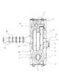
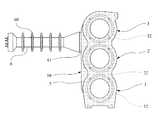
図1は本発明の好適な一実施の形態を示している。本形態において、モールド変圧器は、2次コイルに直流高電圧が重畳し、その直流高電圧が重畳する2次側は樹脂材料による成形体(モールド5)内に埋め込み状態に形成する構成であり、モールド5内に、3相変圧器のための各相2次コイル12,22,32および単相変圧器のための単相2次コイル42を配置し、さらにモールド5から連なる状態にブッシング6を一体に形成し、モールド5の3相側および単相側とにそれぞれ1次コイルおよび鉄心7が組み付く構成になっている。 FIG. 1 shows a preferred embodiment of the present invention. In this embodiment, the mold transformer has a configuration in which a direct current high voltage is superimposed on the secondary coil, and the secondary side on which the direct current high voltage is superimposed is formed in an embedded state in a molded body (mold 5) made of a resin material. In the
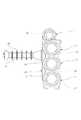
2次コイルに重畳することになる直流高電圧は、例えば200〜300kV程度となる。そこで絶縁性を良好に得るため、2次側のコイルはモールド5内に埋め込んでおり、モールド5は、各2次コイルを埋め込んだ筒状部位が順に積み重なっていて、図2に示すように、u相(第1相)の筒状部位1とv相(第2相)の筒状部位2とw相(第3相)の筒状部位3と単相の筒状部位4とが順に積み重なる形状の本体側からブッシング6が突き出して連なる形状になっている。 The high DC voltage to be superimposed on the secondary coil is, for example, about 200 to 300 kV. Therefore, in order to obtain good insulation, the secondary side coil is embedded in the
各筒状部位1,2,3,4には中央の孔部に、U相1次コイル11,V相1次コイル21,W相1次コイル31,単相1次コイル41をそれぞれ配置し、さらにそれぞれ中央に鉄心7が配置される。 A U-phase
1次コイルおよび2次コイルは、平角線材などの線材を巻き回すことにより形成している。モールド5内に埋め込み状態に形成する2次側は、3相変圧器のための各相ではそれぞれ2つのコイルを有し、図3,図4に示すように、2次コイルaおよび2次コイルbを同心に重ねて形成するが、これら2次コイルa,bに対しては、端縁に絶縁性の帯部材8を配置し、そして導電性テープ9を巻き回して外面の全域を覆い包んで導電性膜層とする構成になっている。 The primary coil and the secondary coil are formed by winding a wire such as a flat wire. The secondary side formed in the embedded state in the
帯部材8はゴム材料や樹脂材料等からなり、その断面を半円形に形成してあって2次コイルa,bの端縁と接しない側で緩やかな凸曲面形状を得るようになっている。 The
導電性テープ9は、例えばカーボン材料からなるカーボンテープとし、モールド5をなす樹脂材料と接着性が良好な材料から形成している。この導電性テープ9による導電性膜層は、当該内側のコイルaあるいはコイルbの一所と結線して電気的に接続している。 The
モールド5は例えばエポキシ樹脂と充填材との混合樹脂などから形成し、成形には、コイルa,コイルbと帯部材8との組み体に対して導電性テープ9を巻き回して外面の全域を覆い包んだ構成物を金型内にセットし、そこへ混合樹脂を注入して埋め込み状態とし、熱硬化させる。なお、モールド5には、1次コイルおよび鉄心7を支持させる金具の取り付け部を設け、1次コイルおよび鉄心7はその金具により所定に組み付けする。 The
各相2次コイルから延びる引き出し線はブッシング6に収容させており、ブッシング6には所定の全長に多数のフランジ60を設け、沿面距離を長くして絶縁性を高めている。そして、モールド5の本体側の表面には導電性塗料50を塗布し、当該塗布表面を接地線へ電気的に接続している。 Lead wires extending from the secondary coils of each phase are accommodated in the
ブッシング6は、図5に拡大して示すように、その根元についてモールド5の本体側の外径を太くした略テーパ形状に形成し、その略テーパ形状の根元には当該部位を周回する溝部61を設けている。溝部61は好ましくは断面を略半円形状に形成する。そして、導電性塗料50は、モールド5の本体側の表面から溝部61の底まで到達させるように塗布する。 As shown in an enlarged view in FIG. 5, the
このように、本発明に係るモールド変圧器では、樹脂材料による成形体(モールド5)には各相2次コイル12,22,32および単相2次コイル42を埋め込ませるとともに、それら2次コイルから延びる引き出し線を収容させるブッシング6も一体に形成するので、引き出し線の接続部分がモールド5に収まり露出せず、したがって、直流高電圧に対して絶縁性を高く得ることができる。そして、モールド5の本体側の表面に導電性塗料50を塗布し、当該塗布表面は接地線へ電気的に接続するので、モールド5の本体側の表面は全域が接地層となり、このため、直流高電圧に係る電界の変動があっても電荷の帯電や放電を防ぐことができる。その結果、帯電,放電に伴う空電音が生じなく、モールド5をなす樹脂材料の劣化を防止でき、絶縁性を高く得ることができ、直流高電圧が重畳するような使用が良好に行える。 As described above, in the molded transformer according to the present invention, the
モールド5内には3相変圧器のための構成とともに、単相変圧器のための構成も含めて埋め込み状態に一体化させるので、全体を小型化することができる。また、モールド5には1次コイルおよび鉄心7を支持させる金具の取り付け部を設けるので、1次コイルおよび鉄心7などの構成要素はモールド5に対して金具により所定に組み付けでき、組み立て性がよい。 Since the
また、ブッシング6の根元はモールド5の本体側の外径を太くした略テーパ形状に形成するので、モールド5の形成においては樹脂材料の熱硬化に伴う収縮の応力が分散し、局部的に残留応力が高くなる部位が生じることがなく、ブッシング6の根元の機械的な強度を向上できる。したがって、当該根元部分の亀裂などの損傷を防止でき、絶縁性について信頼性を高く保つことができる。 Further, since the base of the
また、ブッシング6の根元には当該部位を周回する溝部61を設けて当該溝部61の底までを導電性塗膜面つまり接地膜層とするので、非接地側の表面との境界について電界の集中を緩和でき、溝部61は断面を略半円形状に形成するので境界が穏やかな曲面で連なり、これは電界の局所的な集中を防止する面で有利になる。その結果、直流高電圧に係る電界の変動があっても電荷の帯電や放電を防ぐことができ、帯電,放電に伴う空電音が生じなく、モールド5をなす樹脂材料の劣化を防止でき、直流高電圧に対して絶縁を良好に得ることができる。 Further, since the
なお、本発明に係る構成としては、図6に示すように、単相変圧器を削除した構成を採ることもよく、モールド5には3相変圧器のための各相コイル12,22,32のみを埋め込み状態に一体化させることもできる。 As shown in FIG. 6, the configuration according to the present invention may be a configuration in which the single-phase transformer is omitted, and the
1,2,3,4 筒状部位
5 モールド(成形体)
6 ブッシング
7 鉄心
8 帯部材
9 導電性テープ
11 U相1次コイル
12 u相2次コイル
21 V相1次コイル
22 v相2次コイル
31 W相1次コイル
32 w相2次コイル
41 単相1次コイル
42 単相2次コイル
50 導電性塗料
60 フランジ
61 溝部
a,b 2次コイル
1, 2, 3, 4
6 Bushing 7
Claims (5)
Translated fromJapanese前記成形体内に、3相変圧器のための第1相コイルと第2相コイルと第3相コイルとを埋め込み状態に一体化させるとともに、それら各相コイルから延びる引き出し線をブッシングに収容させ、当該ブッシングは前記成形体から連なり一体に形成し、前記直流高電圧に対して絶縁を得るため所定全長に多数のフランジを設け、前記成形体の本体側表面には導電性塗料を塗布して当該塗布表面を接地線へ電気的に接続するようにし、
前記1次コイル並びに前記2次コイルの鉄心は、前記成形体に組み付け、
前記1次コイルあるいは前記2次コイルのうち直流高電圧が重畳しないコイルは樹脂材料で埋め込むことなく前記成形体に組み付けることを特徴とするモールド変圧器。In a mold transformer in which a DC high voltage is superimposed on at least one of the primary coil or the secondary coil, and the side on which the DC high voltage is superimposed is formed in an embedded state in a molded body made of a resin material.
In the molded body, the first phase coil, the second phase coil, and the third phase coil for the three-phase transformer are integrated in an embedded state, and lead wires extending from the respective phase coils are accommodated in the bushing, The bushing is formed integrally with the molded body, provided with a plurality of flanges over a predetermined length in order to obtain insulation against the DC high voltage, and a conductive paint is applied to the surface of the molded body on the main body side. Makesure that the application surface is electrically connected to the ground wire,
The primary coil and the iron core of the secondary coil are assembled to the molded body,
The molded transformer characterized in that acoil in which a direct current high voltage does not overlap among the primary coil or the secondary coil is assembled to themolded body without being embedded with a resin material .
Priority Applications (1)
| Application Number | Priority Date | Filing Date | Title |
|---|---|---|---|
| JP2006200519AJP4827131B2 (en) | 2006-07-24 | 2006-07-24 | Molded transformer |
Applications Claiming Priority (1)
| Application Number | Priority Date | Filing Date | Title |
|---|---|---|---|
| JP2006200519AJP4827131B2 (en) | 2006-07-24 | 2006-07-24 | Molded transformer |
Publications (2)
| Publication Number | Publication Date |
|---|---|
| JP2008028222A JP2008028222A (en) | 2008-02-07 |
| JP4827131B2true JP4827131B2 (en) | 2011-11-30 |
Family
ID=39118539
Family Applications (1)
| Application Number | Title | Priority Date | Filing Date |
|---|---|---|---|
| JP2006200519AActiveJP4827131B2 (en) | 2006-07-24 | 2006-07-24 | Molded transformer |
Country Status (1)
| Country | Link |
|---|---|
| JP (1) | JP4827131B2 (en) |
Families Citing this family (2)
| Publication number | Priority date | Publication date | Assignee | Title |
|---|---|---|---|---|
| JP5408763B2 (en)* | 2008-03-18 | 2014-02-05 | タカオカ化成工業株式会社 | Mold surface treatment method for mold transformer |
| ES2767340T3 (en)* | 2014-09-29 | 2020-06-17 | Siemens Ag | Feeding system |
Family Cites Families (6)
| Publication number | Priority date | Publication date | Assignee | Title |
|---|---|---|---|---|
| JPS5864010A (en)* | 1981-10-13 | 1983-04-16 | Toshiba Corp | Leading out device of lead wire in oil for electric induction apparatus |
| JPS59177923A (en)* | 1983-03-28 | 1984-10-08 | Matsushita Electronics Corp | Boron diffusion to semiconductor |
| JPS6197820A (en)* | 1984-10-18 | 1986-05-16 | Nippon Telegr & Teleph Corp <Ntt> | Manufacture of thin film and device therefor |
| JPH05176540A (en)* | 1991-12-25 | 1993-07-13 | Toshiba Corp | High voltage generator |
| JPH0870508A (en)* | 1994-08-31 | 1996-03-12 | Toshiba Corp | Switchgear |
| JP2005019455A (en)* | 2003-06-23 | 2005-01-20 | Iq Four:Kk | High-voltage transformer |
- 2006
- 2006-07-24JPJP2006200519Apatent/JP4827131B2/enactiveActive
Also Published As
| Publication number | Publication date |
|---|---|
| JP2008028222A (en) | 2008-02-07 |
Similar Documents
| Publication | Publication Date | Title |
|---|---|---|
| US20160190891A1 (en) | Rotary electric machine stator and manufacturing method of same | |
| JP7004766B2 (en) | Compressor drive with insulation | |
| US2583804A (en) | Motor winding | |
| US10902993B2 (en) | Inductor assembly comprising at least one inductor coil thermally coupled to a metallic inductor housing | |
| JP6588042B2 (en) | Inductor assembly comprising at least one inductor coil thermally coupled to a metal inductor housing | |
| JP2013115832A (en) | Motor | |
| JP4827131B2 (en) | Molded transformer | |
| JP2008187015A (en) | High voltage resin mold transformer | |
| JP7248381B2 (en) | Static induction device | |
| JP2015133777A (en) | Connection method of power cable, and connection structure of power cable | |
| JP2018046264A (en) | Molded coil, transformer, and reactance | |
| CN108369855B (en) | Dry cast transformers with flexible connection terminals | |
| US7477126B2 (en) | Winding for a transformer or a coil and method for the production thereof | |
| JP5408763B2 (en) | Mold surface treatment method for mold transformer | |
| KR102744079B1 (en) | Stator | |
| JP2008028221A (en) | Mold transformer | |
| JP5361225B2 (en) | Mold processing method of mold transformer | |
| CN109802351B (en) | Fully dry cable termination and cable assembly and methods of making, assembling or modifying the same | |
| KR100761008B1 (en) | Molding method of transformer transformer for power supply | |
| JP4939989B2 (en) | Cast insulation | |
| JP2014187763A (en) | Stator | |
| JP2007103933A (en) | Ignition coil for internal combustion engine | |
| CN101965618B (en) | Conductor connection on transformers | |
| JP7310476B2 (en) | Coil end discharge prevention structure | |
| JPH11224824A (en) | Ignition coil |
Legal Events
| Date | Code | Title | Description |
|---|---|---|---|
| A621 | Written request for application examination | Free format text:JAPANESE INTERMEDIATE CODE: A621 Effective date:20090326 | |
| A977 | Report on retrieval | Free format text:JAPANESE INTERMEDIATE CODE: A971007 Effective date:20101222 | |
| A131 | Notification of reasons for refusal | Free format text:JAPANESE INTERMEDIATE CODE: A131 Effective date:20110105 | |
| A521 | Request for written amendment filed | Free format text:JAPANESE INTERMEDIATE CODE: A523 Effective date:20110304 | |
| TRDD | Decision of grant or rejection written | ||
| A01 | Written decision to grant a patent or to grant a registration (utility model) | Free format text:JAPANESE INTERMEDIATE CODE: A01 Effective date:20110908 | |
| A01 | Written decision to grant a patent or to grant a registration (utility model) | Free format text:JAPANESE INTERMEDIATE CODE: A01 | |
| A61 | First payment of annual fees (during grant procedure) | Free format text:JAPANESE INTERMEDIATE CODE: A61 Effective date:20110908 | |
| FPAY | Renewal fee payment (event date is renewal date of database) | Free format text:PAYMENT UNTIL: 20140922 Year of fee payment:3 | |
| R150 | Certificate of patent or registration of utility model | Ref document number:4827131 Country of ref document:JP Free format text:JAPANESE INTERMEDIATE CODE: R150 Free format text:JAPANESE INTERMEDIATE CODE: R150 | |
| R250 | Receipt of annual fees | Free format text:JAPANESE INTERMEDIATE CODE: R250 | |
| R250 | Receipt of annual fees | Free format text:JAPANESE INTERMEDIATE CODE: R250 | |
| R250 | Receipt of annual fees | Free format text:JAPANESE INTERMEDIATE CODE: R250 | |
| R250 | Receipt of annual fees | Free format text:JAPANESE INTERMEDIATE CODE: R250 | |
| R250 | Receipt of annual fees | Free format text:JAPANESE INTERMEDIATE CODE: R250 | |
| R250 | Receipt of annual fees | Free format text:JAPANESE INTERMEDIATE CODE: R250 |