JP4823466B2 - Epitaxial growth substrate and semiconductor device - Google Patents
Epitaxial growth substrate and semiconductor deviceDownload PDFInfo
- Publication number
- JP4823466B2 JP4823466B2JP2002366679AJP2002366679AJP4823466B2JP 4823466 B2JP4823466 B2JP 4823466B2JP 2002366679 AJP2002366679 AJP 2002366679AJP 2002366679 AJP2002366679 AJP 2002366679AJP 4823466 B2JP4823466 B2JP 4823466B2
- Authority
- JP
- Japan
- Prior art keywords
- group iii
- iii nitride
- film
- nitride film
- substrate
- Prior art date
- Legal status (The legal status is an assumption and is not a legal conclusion. Google has not performed a legal analysis and makes no representation as to the accuracy of the status listed.)
- Expired - Lifetime
Links
- 239000000758substrateSubstances0.000titleclaimsdescription78
- 239000004065semiconductorSubstances0.000titleclaimsdescription14
- 150000004767nitridesChemical class0.000claimsdescription63
- IJGRMHOSHXDMSA-UHFFFAOYSA-NAtomic nitrogenChemical compoundN#NIJGRMHOSHXDMSA-UHFFFAOYSA-N0.000claimsdescription10
- 230000003746surface roughnessEffects0.000claimsdescription7
- 229910052757nitrogenInorganic materials0.000claimsdescription5
- 238000005229chemical vapour depositionMethods0.000claimsdescription4
- 239000000463materialSubstances0.000claimsdescription2
- 239000013078crystalSubstances0.000description24
- 238000004519manufacturing processMethods0.000description5
- QGZKDVFQNNGYKY-UHFFFAOYSA-NAmmoniaChemical compoundNQGZKDVFQNNGYKY-UHFFFAOYSA-N0.000description4
- 229910052594sapphireInorganic materials0.000description4
- 239000010980sapphireSubstances0.000description4
- 230000000052comparative effectEffects0.000description3
- 238000010586diagramMethods0.000description3
- 238000010438heat treatmentMethods0.000description3
- 229910021529ammoniaInorganic materials0.000description2
- 230000015572biosynthetic processEffects0.000description2
- 230000000694effectsEffects0.000description2
- 238000002488metal-organic chemical vapour depositionMethods0.000description2
- 238000005121nitridingMethods0.000description2
- JLTRXTDYQLMHGR-UHFFFAOYSA-NtrimethylaluminiumChemical compoundC[Al](C)CJLTRXTDYQLMHGR-UHFFFAOYSA-N0.000description2
- 238000004833X-ray photoelectron spectroscopyMethods0.000description1
- 239000000654additiveSubstances0.000description1
- 230000000996additive effectEffects0.000description1
- 238000004458analytical methodMethods0.000description1
- 239000012159carrier gasSubstances0.000description1
- 230000000295complement effectEffects0.000description1
- 230000007547defectEffects0.000description1
- 238000001514detection methodMethods0.000description1
- 238000011156evaluationMethods0.000description1
- 230000005284excitationEffects0.000description1
- 229910052733galliumInorganic materials0.000description1
- 230000017525heat dissipationEffects0.000description1
- 239000001257hydrogenSubstances0.000description1
- 229910052739hydrogenInorganic materials0.000description1
- 125000004435hydrogen atomChemical class[H]*0.000description1
- 239000012535impuritySubstances0.000description1
- 229910052738indiumInorganic materials0.000description1
- 238000005259measurementMethods0.000description1
- 238000000034methodMethods0.000description1
- 238000012986modificationMethods0.000description1
- 230000004048modificationEffects0.000description1
- 239000002994raw materialSubstances0.000description1
- 235000013619trace mineralNutrition0.000description1
- 239000011573trace mineralSubstances0.000description1
- 229910052725zincInorganic materials0.000description1
Images

Classifications
- C—CHEMISTRY; METALLURGY
- C30—CRYSTAL GROWTH
- C30B—SINGLE-CRYSTAL GROWTH; UNIDIRECTIONAL SOLIDIFICATION OF EUTECTIC MATERIAL OR UNIDIRECTIONAL DEMIXING OF EUTECTOID MATERIAL; REFINING BY ZONE-MELTING OF MATERIAL; PRODUCTION OF A HOMOGENEOUS POLYCRYSTALLINE MATERIAL WITH DEFINED STRUCTURE; SINGLE CRYSTALS OR HOMOGENEOUS POLYCRYSTALLINE MATERIAL WITH DEFINED STRUCTURE; AFTER-TREATMENT OF SINGLE CRYSTALS OR A HOMOGENEOUS POLYCRYSTALLINE MATERIAL WITH DEFINED STRUCTURE; APPARATUS THEREFOR
- C30B25/00—Single-crystal growth by chemical reaction of reactive gases, e.g. chemical vapour-deposition growth
- C30B25/02—Epitaxial-layer growth
- C30B25/18—Epitaxial-layer growth characterised by the substrate
- C—CHEMISTRY; METALLURGY
- C30—CRYSTAL GROWTH
- C30B—SINGLE-CRYSTAL GROWTH; UNIDIRECTIONAL SOLIDIFICATION OF EUTECTIC MATERIAL OR UNIDIRECTIONAL DEMIXING OF EUTECTOID MATERIAL; REFINING BY ZONE-MELTING OF MATERIAL; PRODUCTION OF A HOMOGENEOUS POLYCRYSTALLINE MATERIAL WITH DEFINED STRUCTURE; SINGLE CRYSTALS OR HOMOGENEOUS POLYCRYSTALLINE MATERIAL WITH DEFINED STRUCTURE; AFTER-TREATMENT OF SINGLE CRYSTALS OR A HOMOGENEOUS POLYCRYSTALLINE MATERIAL WITH DEFINED STRUCTURE; APPARATUS THEREFOR
- C30B29/00—Single crystals or homogeneous polycrystalline material with defined structure characterised by the material or by their shape
- C30B29/10—Inorganic compounds or compositions
- C30B29/40—AIIIBV compounds wherein A is B, Al, Ga, In or Tl and B is N, P, As, Sb or Bi
- C30B29/403—AIII-nitrides
- H—ELECTRICITY
- H01—ELECTRIC ELEMENTS
- H01L—SEMICONDUCTOR DEVICES NOT COVERED BY CLASS H10
- H01L21/00—Processes or apparatus adapted for the manufacture or treatment of semiconductor or solid state devices or of parts thereof
- H01L21/02—Manufacture or treatment of semiconductor devices or of parts thereof
- H01L21/02104—Forming layers
- H01L21/02365—Forming inorganic semiconducting materials on a substrate
- H01L21/02367—Substrates
- H01L21/0237—Materials
- H01L21/02373—Group 14 semiconducting materials
- H01L21/02378—Silicon carbide
- H—ELECTRICITY
- H01—ELECTRIC ELEMENTS
- H01L—SEMICONDUCTOR DEVICES NOT COVERED BY CLASS H10
- H01L21/00—Processes or apparatus adapted for the manufacture or treatment of semiconductor or solid state devices or of parts thereof
- H01L21/02—Manufacture or treatment of semiconductor devices or of parts thereof
- H01L21/02104—Forming layers
- H01L21/02365—Forming inorganic semiconducting materials on a substrate
- H01L21/02367—Substrates
- H01L21/02428—Structure
- H01L21/0243—Surface structure
- H—ELECTRICITY
- H01—ELECTRIC ELEMENTS
- H01L—SEMICONDUCTOR DEVICES NOT COVERED BY CLASS H10
- H01L21/00—Processes or apparatus adapted for the manufacture or treatment of semiconductor or solid state devices or of parts thereof
- H01L21/02—Manufacture or treatment of semiconductor devices or of parts thereof
- H01L21/02104—Forming layers
- H01L21/02365—Forming inorganic semiconducting materials on a substrate
- H01L21/02436—Intermediate layers between substrates and deposited layers
- H01L21/02439—Materials
- H01L21/02455—Group 13/15 materials
- H01L21/02458—Nitrides
- H—ELECTRICITY
- H01—ELECTRIC ELEMENTS
- H01L—SEMICONDUCTOR DEVICES NOT COVERED BY CLASS H10
- H01L21/00—Processes or apparatus adapted for the manufacture or treatment of semiconductor or solid state devices or of parts thereof
- H01L21/02—Manufacture or treatment of semiconductor devices or of parts thereof
- H01L21/02104—Forming layers
- H01L21/02365—Forming inorganic semiconducting materials on a substrate
- H01L21/02518—Deposited layers
- H01L21/02521—Materials
- H01L21/02538—Group 13/15 materials
- H01L21/0254—Nitrides
- H—ELECTRICITY
- H01—ELECTRIC ELEMENTS
- H01L—SEMICONDUCTOR DEVICES NOT COVERED BY CLASS H10
- H01L21/00—Processes or apparatus adapted for the manufacture or treatment of semiconductor or solid state devices or of parts thereof
- H01L21/02—Manufacture or treatment of semiconductor devices or of parts thereof
- H01L21/02104—Forming layers
- H01L21/02365—Forming inorganic semiconducting materials on a substrate
- H01L21/02612—Formation types
- H01L21/02617—Deposition types
- H01L21/0262—Reduction or decomposition of gaseous compounds, e.g. CVD
- Y—GENERAL TAGGING OF NEW TECHNOLOGICAL DEVELOPMENTS; GENERAL TAGGING OF CROSS-SECTIONAL TECHNOLOGIES SPANNING OVER SEVERAL SECTIONS OF THE IPC; TECHNICAL SUBJECTS COVERED BY FORMER USPC CROSS-REFERENCE ART COLLECTIONS [XRACs] AND DIGESTS
- Y10—TECHNICAL SUBJECTS COVERED BY FORMER USPC
- Y10T—TECHNICAL SUBJECTS COVERED BY FORMER US CLASSIFICATION
- Y10T428/00—Stock material or miscellaneous articles
- Y10T428/12—All metal or with adjacent metals
- Y10T428/12493—Composite; i.e., plural, adjacent, spatially distinct metal components [e.g., layers, joint, etc.]
- Y10T428/12528—Semiconductor component
- Y—GENERAL TAGGING OF NEW TECHNOLOGICAL DEVELOPMENTS; GENERAL TAGGING OF CROSS-SECTIONAL TECHNOLOGIES SPANNING OVER SEVERAL SECTIONS OF THE IPC; TECHNICAL SUBJECTS COVERED BY FORMER USPC CROSS-REFERENCE ART COLLECTIONS [XRACs] AND DIGESTS
- Y10—TECHNICAL SUBJECTS COVERED BY FORMER USPC
- Y10T—TECHNICAL SUBJECTS COVERED BY FORMER US CLASSIFICATION
- Y10T428/00—Stock material or miscellaneous articles
- Y10T428/26—Web or sheet containing structurally defined element or component, the element or component having a specified physical dimension
- Y10T428/263—Coating layer not in excess of 5 mils thick or equivalent
- Y10T428/264—Up to 3 mils
- Y10T428/265—1 mil or less
Landscapes
- Engineering & Computer Science (AREA)
- Chemical & Material Sciences (AREA)
- Condensed Matter Physics & Semiconductors (AREA)
- Power Engineering (AREA)
- Microelectronics & Electronic Packaging (AREA)
- Computer Hardware Design (AREA)
- Manufacturing & Machinery (AREA)
- General Physics & Mathematics (AREA)
- Physics & Mathematics (AREA)
- Materials Engineering (AREA)
- Crystallography & Structural Chemistry (AREA)
- Organic Chemistry (AREA)
- Metallurgy (AREA)
- General Chemical & Material Sciences (AREA)
- Chemical Kinetics & Catalysis (AREA)
- Inorganic Chemistry (AREA)
- Crystals, And After-Treatments Of Crystals (AREA)
- Chemical Vapour Deposition (AREA)
Description
Translated fromJapanese【0001】
【発明の属する技術分野】
本発明は、各種半導体素子の基板として好適に用いることのできるエピタキシャル成長用基板に関する。
【0002】
【従来の技術】
Alを含むIII族窒化物膜は、半導体発光素子や半導体受光素子を構成する半導体膜あるいはその半導体膜成長用の下地膜として用いられており、近年においては、携帯電話などに用いられる高速ICチップなどの電子デバイスや、短波長LEDなどを構成する半導体膜としても注目を浴びている。
【0003】
上記半導体素子は、サファイア単結晶などからなる単結晶基板上に、必要に応じてIII族窒化物からなる緩衝膜を形成した後、この緩衝膜上に同じくAl含有III族窒化物膜からなる下地膜を形成し、この下地膜上に目的とする機能を有する各種III族窒化物膜を形成することによって得る。また、通常においては、前記基板、前記緩衝膜、及び前記下地膜を一体と見なし、これをエピタキシャル成長用基板として呼んでいる。
【0004】
前記緩衝膜は、前記基板と前記下地膜との格子定数差を補完して緩衝効果を発揮させるべく、その結晶性を無視して500〜700℃の低温において、MOCVD法によって形成される。
【0005】
また、放熱性に優れ、サファイア単結晶よりも格子定数がIII族窒化物膜に近いことからSiC基板を用い、このSiC基板上にAlNからなる緩衝膜あるいは下地膜を形成する場合もある。この場合、前記緩衝膜及び前記下地膜は、1000℃以上の高温でにおいてMOCVD法によって形成される。
【0006】
【発明が解決しようとする課題】
しかしながら、サファイア基板を用いた場合、緩衝膜は上述したような低温度で形成されるために結晶性が低く、前記緩衝膜上に形成した下地膜及び各種機能が付与されたAl含有窒化物膜の結晶性を十分に高めることができないでいた。さらに、前記緩衝膜中には比較的多量の転位が存在するため、前記下地膜及び前記Al含有半導体膜にも前記転位に起因した多量の転位が生成されてしまうとともに、X線ロッキングカーブで評価することのできるモザイク性が大きくなってしまっていた。さらに緩衝膜形成とIII族窒化物膜形成との間の温度履歴により、Al含有III族窒化物膜の結晶性や転位密度などの結晶品質が大きくばらついてしまうという問題もあった。
【0007】
この結果、各種機能が付与されたAl含有III族窒化物膜の結晶性や転位密度などの結晶品質を十分に高めることができず、これらのAl含有III族窒化物膜を含む半導体素子、例えば半導体発光素子などにおいては、その発光効率が劣化してしまうという問題があった。
【0008】
また、SiC基板を用いた場合、高温で成膜したAlNからなる前記緩衝膜や前記下地膜は、0.1μm程度の厚さしか有しないため、結晶性において不十分であり、ピットなどが発生することにより表面平坦性も不十分なものであった。また、SiC基板表面に存在する欠陥の影響を受けやすいという問題もあった。
【0009】
本発明は、所定の単結晶基板上において、高い結晶品質のAl含有III族窒化物膜を形成することが可能なエピタキシャル成長用基板を提供することを目的とする。
【0010】
【課題を解決するための手段】
上記目的を達成すべく、本発明は、6H−SiC基板と、このSiC基板上に形成された、少なくともAlを含み、転位密度が1.0×10¹¹/cm2以下であって、(002)面におけるX線ロッキングカーブ半値幅が200秒以下であり、(102)面におけるX線ロッキングカーブ半値幅が1500秒以下であるIII族窒化物膜とを具え、前記III族窒化物膜の厚さが0.2μm以上であり、前記III族窒化物膜の表面粗さが3Å以下であり、前記III族窒化物膜はAlNから構成され、前記6H−SiC基板はその主面上に表面窒化層を有し、前記III族窒化物膜は前記表面窒化層を介して形成されたことを特徴とする、エピタキシャル成長用基板に係るものである。
【0011】
本発明者らは、単結晶基板上において結晶品質に優れたAl含有III族窒化物膜を形成すべく鋭意検討を実施した。その結果、従来のサファイア単結晶基板などに代えて6H−SiC基板を用い、この基板上に所定の条件で少なくともAlを含むIII族窒化物膜を少なくとも0.2μm以上の厚さで形成することにより、前記III族窒化物膜の転位密度及び結晶性を著しく向上させることができ、結晶品質に優れ、かつクラックの存在しないエピタキシャル成長用基板を提供できることを想到した。
【0012】
すなわち、基板として6H−SiC基板を用い、この基板上に所定の作製条件を満足するように比較的多量のAlを含むIII族窒化物膜を形成することによって、前記III族窒化物膜の結晶品質、しいてはエピタキシャル成長用基板の結晶品質を向上できることを見出した。
【0013】
このように本発明のエピタキシャル成長用基板は優れた結晶品質を有するので、前記基板上に目的とするAl含有III族窒化物膜を作製した場合において、その結晶品質を著しく向上させることができるようになる。したがって、最終的に得た半導体素子などの特性も著しく向上させることができるようになる。
【0014】
なお、本発明の好ましい態様においては、前記6H−SiC基板の主面に対して表面窒化処理を施し、表面窒化層を形成することが好ましい。これによって、前記基板上に形成する前記III族窒化物膜の結晶品質をより向上させることができる。
【0015】
【発明の実施の形態】
以下、本発明を発明の実施の形態に即して詳細に説明する。
図1は、本発明にかかるエピタキシャル成長用基板の構成を示す概略図である。図1に示すエピタキシャル成長用基板10は、6H−SiC基板1と、この基板上に形成された少なくともAlを含むIII族窒化物膜2とから構成されている。
【0016】
III族窒化物膜2はAlを含むことが必要であり、一般的にはAlxGayInzN(0≦x,y,z≦1,x+y+z=1)なる組成式で表すことができる。また、Al含有量はIII族窒化物膜2中における全III族元素に対して50原子%以上(x≧0.5)であることが好ましいが、本発明では、さらにはIII族窒化物膜2中におけるIII族元素の総てがAlより構成され(x=1)、AlNから構成される。
【0017】
図1に示すエピタキシャル成長用基板10においては、6H−SiC基板1を用いるとともに、上述のように比較的多量のAlを含むIII族窒化物膜2を有しているので、所定の作製条件を満足することにより、III族窒化物膜2中における転位密度を1×10¹¹/cm2以下、好ましくは5×1011/cm2以下、さらに好ましくは1×1010/cm2以下に設定することができる。
【0018】
また、III族窒化物膜2の結晶性は、(002)面におけるロッキングカーブ半値幅が200秒以下、好ましくは150秒以下となるように設定することができる。さらに、(102)面におけるロッキングカーブ半値幅が1500秒以下、好ましくは1200秒以下、さらに好ましくは1000秒以下となるように設定することができる。
【0019】
さらには、作製条件を適宜に設定することにより、III族窒化物膜2の表面粗さRaを5μm2の領域内において、3Å以下にまですることができる。この場合、表面には数層の原子層から構成される原子ステップが観察される。
【0020】
同様に、III族窒化物膜2の厚さを0.2μm以上、好ましくは0.3μm以上、さらに好ましくは0.4μm以上に設定することができる。従来においては、SiC基板を用い、前記基板上にIII族窒化物膜を0.2μm以上の厚さに形成すると、前記III族窒化物膜中にはクラックが発生してしまっていたが、本発明においては、III族窒化物膜の厚さを0.2μm以上としてもクラックの発生を抑制することができる。なお、III族窒化物膜2の厚さは1.2μm以下であることが好ましい。これより厚くなると、作製条件によってはクラックが発生してしまう場合がある。
【0021】
但し、このようなクラックの発生を抑制するため、前記III族窒化物膜中のAl組成を、その厚さ方向において、6H−SiC基板側からその反対側の膜表面に向けて、連続的又はステップ状に減少させることができる。この場合、クラックの発生する臨界膜厚をより増大させることができ、前記III族窒化物膜の厚さを1.2μm以上とすることができる。
【0022】
このように、図1に示す本発明の参考例のエピタキシャル成長用基板10は、その表面に結晶品質に優れたIII族窒化物膜2を有するので、所定のIII族窒化物膜を形成した場合において、その結晶品質を向上させることができ、目的とする半導体素子を作製した場合において、その特性を向上させることができるようになる。
【0023】
上述した要件を満足するIII族窒化物膜2は、公知の成膜手法を用いて形成することができるが、6H−SiC基板1を1100℃以上、さらには1200℃以上、特には1300℃以上に加熱した状態において、CVD法を用いて形成することが好ましい。これによって、上述した要件を満足したIII族窒化物膜2を簡易に形成することができるようになる。なお、上記温度は、6H−SiC基板1自身の設定温度である。
【0024】
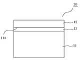
図2は、本発明のエピタキシャル成長用基板における構成を示す概略図である。図2に示すエピタキシャル成長用基板20は、6H−SiC基板11と、この基板の主面11Aに形成された表面窒化層13を介して形成された少なくともAlを含むIII族窒化物膜12とから構成されている。本例におけるエピタキシャル成長用基板20においては、III族窒化物膜12は表面窒化層13を介して形成されているので、その結晶品質をより簡易に向上させることができる。また、クラックの発生を効果的に抑制することができる。
【0025】
表面窒化層13は、6H−SiC基板11をアンモニアなどの活性窒素含有雰囲気中に配置するとともに、1100℃以上に加熱することによって形成することができる。
【0026】
また、表面窒化層13の表面での窒素モル分率は3%以上、さらには5%以上であることが望ましい。これによって、III族窒化物膜12の結晶品質をより効果的に向上させ、クラックの発生を効果的に抑制することができる。
【0027】
なお、本発明における「窒素モル分率」とはESCAによる組成分析の結果から導出したものである。この測定は、Quantra SXM(PHI社製)の装置を用い、励起X線としてX線径200μmのAlKα1,2線(1486.6eV)を用いて、光電子検出角度45°にて実施した。
【0028】
なお、III族窒化物膜12に要求される要件は、図1に示すIII族窒化物膜2に要求される要件と同じである。また、図1に示すIII族窒化物膜2と同様にCVD法によって形成することができる。
【0029】
【実施例】
(参考例1)
厚さ330μm、直径2インチの6H−SiC基板を反応管内に設置し、前記基板を1150℃に加熱するとともに、トリメチルアルミニウム(TMA)及びアンモニア(NH3)を流速5m/secで前記反応管内に導入することによって前記基板上に0.5μm以上の厚さのAlN膜を各種形成した。なお、前記基板表面の窒素モル分率を測定したところ、2.1%であった。
【0030】
前記AlN膜中の転位密度をTEM観察によって計測したところ、2×10¹⁰/cm2であった。また、前記AlN膜の(002)面におけるX線ロッキングカーブは80秒であり、(102)面におけるX線ロッキングカーブ半値幅は900秒であった。さらに、前記AlN膜の表面粗さは1.5Åであり、明瞭な原子ステップが観察された。また、この成長条件でのクラックの発生する臨界膜厚を調べたところ、0.7μmであることが判明した。
【0031】
(実施例)
参考例1と同じ6H−SiC基板を反応管内に設置し、前記基板を1150℃に加熱するとともに、NH3を水素(H2)キャリアガスとともに導入して前記基板の主面に表面窒化処理を施し、表面窒化層を厚さ1nmに形成した。次いで、参考例1と同条件で0.5μm以上の厚さのAlN膜を各種形成した。なお、別途、前記表面窒化処理のみを加えた基板のみを準備し、その表面のモル分率を測定したところ、10.3%であった。
【0032】
前記AlN膜中の転位密度をTEM観察によって計測したところ、2×10¹⁰/cm2であった。また、前記AlN膜の(002)面におけるX線ロッキングカーブは80秒であり、(102)面におけるX線ロッキングカーブ半値幅は900秒であった。さらに、前記AlN膜の表面粗さは1.5Åであり、明瞭な原子ステップが観察された。また、この成長条件でのクラックの発生する臨界膜厚を調べたところ、1.2μmであることが判明した。
【0033】
(比較例1)
厚さ330μm、直径2インチの4H−SiC基板を用いた以外は、参考例1と同様にしてAlN膜を厚さ0.5μmに形成した。 前記AlN膜中の転位密度をTEM観察によって計測したところ、5×10¹⁰/cm2であった。また、前記AlN膜の(002)面におけるX線ロッキングカーブは400秒であり、(102)面におけるX線ロッキングカーブ半値幅は1200秒であった。さらに、前記AlN膜の表面粗さは3.5Åであり、表面にピットが観察され、明瞭な原子ステップは観察されなかった。
【0034】
(比較例2)
厚さ330μm、直径2インチの4H−SiC基板を用いた以外は、実施例と同様にして、AlN膜を厚さ0.5μmに形成した。前記AlN膜中の転位密度をTEM観察によって計測したところ、5×10¹⁰/cm2であった。また、前記AlN膜の(002)面におけるX線ロッキングカーブは300秒であり、(102)面におけるX線ロッキングカーブ半値幅は1000秒であった。さらに、前記AlN膜の表面粗さは3.5Åであり、表面にピットが観察され、明瞭な原子ステップは観察されなかった。
【0035】
以上、実施例及び比較例から明らかなように、本発明に従って、6H−SiC基板を用い、この基板を1100℃以上に加熱してCVD法により形成したAlN膜は高い結晶品質を呈することが分かる。
【0036】
以上、具体例を挙げながら、発明の実施の形態に基づいて本発明を詳細に説明してきたが、本発明は上記内容に限定されるものではなく、本発明の範疇を逸脱しない範囲であらゆる変更や変形が可能である。
【0037】
例えば、前記III族窒化物膜は、主として上記参考例1のような場合ではあるが、上述したようにAlの他、Ga及びInなどを含むことができる。さらに、必要に応じてGe、Si、Mg、Zn、Be、P、及びBなどの添加元素を含有することもできる。さらに、意識的に添加した元素に限らず、成膜条件などに依存して必然的に取り込まれる微量元素、並びに原料、反応管材質に含まれる微量不純物を含むこともできる。
【0038】
さらに、6H−SiC基板上に、所定の緩衝層やひずみ超格子などの多層積層膜を挿入し、前記基板上に形成すべきIII族窒化物膜の結晶品質をさらに向上させることもできる。また、SiC基板表面に高温還元雰囲気で熱処理を実施し、前記SiC基板表面の改質を行うこともできる。さらに、SiC基板のオフ角度についても適宜に設定することができる。
【0039】
【発明の効果】
以上説明したように、本発明によれば、結晶品質に優れたエピタキシャル成長用基板を提供することができる。
【図面の簡単な説明】
【図1】本発明の参考例のエピタキシャル成長用基板を示す構成図である。
【図2】本発明のエピタキシャル成長用基板の例を示す構成図である。
【符号の説明】
1,11 単結晶基板、2,12 III族窒化物膜、10,20 エピタキシャル成長用基板、13 表面窒化層[0001]
BACKGROUND OF THE INVENTION
The present invention relates to an epitaxial growth substrate that can be suitably used as a substrate for various semiconductor elements.
[0002]
[Prior art]
A group III nitride film containing Al is used as a semiconductor film constituting a semiconductor light-emitting element or semiconductor light-receiving element or a base film for growing the semiconductor film. In recent years, a high-speed IC chip used for a mobile phone or the like. It is also attracting attention as a semiconductor film constituting an electronic device such as a short wavelength LED.
[0003]
In the semiconductor device, a buffer film made of a group III nitride is formed on a single crystal substrate made of sapphire single crystal, if necessary, and then a lower layer made of an Al-containing group III nitride film is also formed on the buffer film. It is obtained by forming a base film and forming various group III nitride films having a desired function on the base film. In general, the substrate, the buffer film, and the base film are regarded as one body, and this is called an epitaxial growth substrate.
[0004]
The buffer film is formed by MOCVD at a low temperature of 500 to 700 ° C., neglecting its crystallinity, in order to complement the lattice constant difference between the substrate and the base film and exhibit a buffer effect.
[0005]
In addition, since the heat dissipation is excellent and the lattice constant is closer to that of the group III nitride film than the sapphire single crystal, a SiC substrate is used, and a buffer film or a base film made of AlN may be formed on the SiC substrate. In this case, the buffer film and the base film are formed by MOCVD at a high temperature of 1000 ° C. or higher.
[0006]
[Problems to be solved by the invention]
However, when a sapphire substrate is used, since the buffer film is formed at a low temperature as described above, the crystallinity is low, and the base film formed on the buffer film and the Al-containing nitride film provided with various functions It was not possible to sufficiently increase the crystallinity. Furthermore, since a relatively large amount of dislocations are present in the buffer film, a large amount of dislocations due to the dislocations are generated in the base film and the Al-containing semiconductor film, and evaluation is performed using an X-ray rocking curve. The mosaic that can be done has increased. Furthermore, there is a problem that the crystal quality of the Al-containing group III nitride film such as crystallinity and dislocation density varies greatly due to the temperature history between the formation of the buffer film and the group III nitride film.
[0007]
As a result, the crystal quality such as crystallinity and dislocation density of the Al-containing group III nitride film to which various functions are imparted cannot be sufficiently improved, and a semiconductor element including these Al-containing group III nitride films, for example, In the semiconductor light emitting device, there is a problem that the light emission efficiency is deteriorated.
[0008]
In addition, when a SiC substrate is used, the buffer film and the base film made of AlN formed at a high temperature have a thickness of about 0.1 μm, so that the crystallinity is insufficient and pits are generated. As a result, the surface flatness was insufficient. There is also a problem that it is easily affected by defects existing on the surface of the SiC substrate.
[0009]
An object of the present invention is to provide an epitaxial growth substrate capable of forming a high crystal quality Al-containing group III nitride film on a predetermined single crystal substrate.
[0010]
[Means for Solving the Problems]
In order to achieve the above object, the present invention includes a 6H—SiC substrate and at least Al formed on the SiC substrate, and a dislocation density of 1.0 × 10¹¹ / cm2 or less, And a group III nitride film having an X-ray rocking curve half-value width in the (102) plane of not more than 200 seconds and a X-ray rocking curve half-value width in the (102) surface of not more than 1500 seconds, and the thickness of the group III nitride film The group III nitride film has a surface roughness of 3 mm or less, the group III nitride film is made of AlN, and the 6H—SiC substrate is surface nitrided on its main surface. And the group III nitride film is formed through the surface nitrided layer, and relates to an epitaxial growth substrate.
[0011]
The present inventors have intensively studied to form an Al-containing group III nitride film having excellent crystal quality on a single crystal substrate. As a result, a 6H—SiC substrate is used instead of the conventional sapphire single crystal substrate, and a group III nitride film containing at least Al is formed on the substrate with a thickness of at least 0.2 μm or more under predetermined conditions. Thus, it has been conceived that the dislocation density and crystallinity of the group III nitride film can be remarkably improved, and an epitaxial growth substrate having excellent crystal quality and free from cracks can be provided.
[0012]
That is, by using a 6H—SiC substrate as a substrate and forming a group III nitride film containing a relatively large amount of Al on the substrate so as to satisfy predetermined manufacturing conditions, the crystal of the group III nitride film is formed. It has been found that the quality, and hence the crystal quality of the epitaxial growth substrate, can be improved.
[0013]
As described above, since the epitaxial growth substrate of the present invention has excellent crystal quality, when the target Al-containing group III nitride film is produced on the substrate, the crystal quality can be remarkably improved. Become. Therefore, the characteristics of the finally obtained semiconductor element can be remarkably improved.
[0014]
In a preferred embodiment of the present invention, it is preferable to subject the main surface of the 6H—SiC substrate to surface nitriding to form a surface nitrided layer. Thereby, the crystal quality of the group III nitride film formed on the substrate can be further improved.
[0015]
DETAILED DESCRIPTION OF THE INVENTION
Hereinafter, the present invention will be described in detail according to embodiments of the invention.
Figure 1 is a schematic diagram showing an epitaxial growth substrate structureaccording to the present invention. An
[0016]
The group III
[0017]
The
[0018]
Further, the crystallinity of the group III
[0019]
Furthermore, the surface roughness Ra of the group
[0020]
Similarly, the thickness of the group
[0021]
However, in order to suppress the occurrence of such cracks, the Al composition in the group III nitride film is continuously or in the thickness direction from the 6H-SiC substrate side to the opposite film surface. It can be reduced in steps. In this case, the critical film thickness at which cracks occur can be further increased, and the thickness of the group III nitride film can be 1.2 μm or more.
[0022]
As described above, sincethe
[0023]
The group
[0024]
FIG. 2 is a schematic view showing theconfiguration of the epitaxial growth substrate of the present invention . An
[0025]
The
[0026]
Further, the nitrogen mole fraction on the surface of the surface nitrided
[0027]
The “nitrogen mole fraction” in the present invention is derived from the result of composition analysis by ESCA. This measurement was performed using an apparatus of Quantra SXM (manufactured by PHI) using AlKα1,2 line (1486.6 eV) having an X-ray diameter of 200 μm as excitation X-rays at a photoelectron detection angle of 45 °.
[0028]
The requirements for the group
[0029]
【Example】
(Reference Example 1)
A 6H—SiC substrate having a thickness of 330 μm and a diameter of 2 inches was placed in the reaction tube, the substrate was heated to 1150 ° C., and trimethylaluminum (TMA) and ammonia (NH3 ) were flown into the reaction tube at a flow rate of 5 m / sec. By introducing, various AlN films having a thickness of 0.5 μm or more were formed on the substrate. The nitrogen mole fraction on the substrate surface was measured and found to be 2.1%.
[0030]
When the dislocation density in the AlN film was measured by TEM observation, it was 2 × 10¹⁰ / cm2 . In addition, the X-ray rocking curve on the (002) plane of the AlN film was 80 seconds, and the half width of the X-ray rocking curve on the (102) plane was 900 seconds. Further, the surface roughness of the AlN film was 1.5 mm, and a clear atomic step was observed. Further, when the critical film thickness at which cracks occur under these growth conditions was examined, it was found to be 0.7 μm.
[0031]
(Example)
The same 6H—SiC substrate as inReference Example 1 was placed in a reaction tube, the substrate was heated to 1150 ° C., and NH3 was introduced together with a hydrogen (H2 ) carrier gas to subject the main surface of the substrate to surface nitridation. The surface nitrided layer was formed to a thickness of 1 nm. Next, various AlN films having a thickness of 0.5 μm or more were formed under the same conditions as inReference Example 1. Separately, only a substrate to which only the surface nitriding treatment was applied was prepared, and the molar fraction of the surface was measured, and it was 10.3%.
[0032]
When the dislocation density in the AlN film was measured by TEM observation, it was 2 × 10¹⁰ / cm2 . In addition, the X-ray rocking curve on the (002) plane of the AlN film was 80 seconds, and the half width of the X-ray rocking curve on the (102) plane was 900 seconds. Further, the surface roughness of the AlN film was 1.5 mm, and a clear atomic step was observed. Further, when the critical film thickness at which cracks occur under these growth conditions was examined, it was found to be 1.2 μm.
[0033]
(Comparative Example 1)
An AlN film was formed to a thickness of 0.5 μm in the same manner as inReference Example 1 except that a 4H—SiC substrate having a thickness of 330 μm and a diameter of 2 inches was used. When the dislocation density in the AlN film was measured by TEM observation, it was 5 × 10¹⁰ / cm2 . Further, the X-ray rocking curve on the (002) plane of the AlN film was 400 seconds, and the half width of the X-ray rocking curve on the (102) plane was 1200 seconds. Furthermore, the surface roughness of the AlN film was 3.5 mm, pits were observed on the surface, and no clear atomic steps were observed.
[0034]
(Comparative Example 2)
An AlN film having a thickness of 0.5 μm was formed in the same manner as in theexample except that a 4H—SiC substrate having a thickness of 330 μm and a diameter of 2 inches was used. When the dislocation density in the AlN film was measured by TEM observation, it was 5 × 10¹⁰ / cm2 . Further, the X-ray rocking curve on the (002) plane of the AlN film was 300 seconds, and the half width of the X-ray rocking curve on the (102) plane was 1000 seconds. Furthermore, the surface roughness of the AlN film was 3.5 mm, pits were observed on the surface, and no clear atomic steps were observed.
[0035]
As can be seen from the examples and comparative examples, according to the present invention, the 6N-SiC substrate is used, and the AlN film formed by the CVD method by heating the substrate to 1100 ° C. or higher exhibits high crystal quality. .
[0036]
As mentioned above, the present invention has been described in detail based on the embodiments of the present invention with specific examples. However, the present invention is not limited to the above contents, and various modifications can be made without departing from the scope of the present invention. And can be modified.
[0037]
For example, although the group III nitride film ismainly in the case of the reference example 1, as described above, it can contain Ga, In, and the like in addition to Al. Furthermore, additive elements such as Ge, Si, Mg, Zn, Be, P, and B can be contained as required. Furthermore, it is possible to include not only elements added intentionally but also trace elements that are inevitably taken in depending on the film forming conditions and the like, as well as trace impurities contained in the raw materials and reaction tube materials.
[0038]
Furthermore, a multilayer film such as a predetermined buffer layer or strained superlattice can be inserted on the 6H—SiC substrate to further improve the crystal quality of the group III nitride film to be formed on the substrate. Also, the SiC substrate surface can be modified by performing a heat treatment on the SiC substrate surface in a high temperature reducing atmosphere. Furthermore, the off-angle of the SiC substrate can also be set as appropriate.
[0039]
【The invention's effect】
As described above, according to the present invention, an epitaxial growth substrate having excellent crystal quality can be provided.
[Brief description of the drawings]
FIG. 1is a configuration diagramshowing an epitaxial growth substrate according to a reference example of the present invention.
FIG. 2 is a configuration diagram showing an example of an epitaxialgrowth substrate of the present invention.
[Explanation of symbols]
1,11 single crystal substrate, 2,12 group III nitride film, 10,20 substrate for epitaxial growth, 13 surface nitride layer
Claims (4)
Translated fromJapanesePriority Applications (3)
| Application Number | Priority Date | Filing Date | Title |
|---|---|---|---|
| JP2002366679AJP4823466B2 (en) | 2002-12-18 | 2002-12-18 | Epitaxial growth substrate and semiconductor device |
| US10/738,187US6869702B2 (en) | 2002-12-18 | 2003-12-17 | Substrate for epitaxial growth |
| EP03257970AEP1431426B1 (en) | 2002-12-18 | 2003-12-17 | Substrate for epitaxial growth |
Applications Claiming Priority (1)
| Application Number | Priority Date | Filing Date | Title |
|---|---|---|---|
| JP2002366679AJP4823466B2 (en) | 2002-12-18 | 2002-12-18 | Epitaxial growth substrate and semiconductor device |
Publications (2)
| Publication Number | Publication Date |
|---|---|
| JP2004200384A JP2004200384A (en) | 2004-07-15 |
| JP4823466B2true JP4823466B2 (en) | 2011-11-24 |
Family
ID=32376266
Family Applications (1)
| Application Number | Title | Priority Date | Filing Date |
|---|---|---|---|
| JP2002366679AExpired - LifetimeJP4823466B2 (en) | 2002-12-18 | 2002-12-18 | Epitaxial growth substrate and semiconductor device |
Country Status (3)
| Country | Link |
|---|---|
| US (1) | US6869702B2 (en) |
| EP (1) | EP1431426B1 (en) |
| JP (1) | JP4823466B2 (en) |
Families Citing this family (13)
| Publication number | Priority date | Publication date | Assignee | Title |
|---|---|---|---|---|
| JP2007059850A (en)* | 2005-08-26 | 2007-03-08 | Ngk Insulators Ltd | Group III nitride film-forming substrate, method of manufacturing the same, and semiconductor device using the same |
| US7723216B2 (en)* | 2006-05-09 | 2010-05-25 | The Regents Of The University Of California | In-situ defect reduction techniques for nonpolar and semipolar (Al, Ga, In)N |
| KR101363316B1 (en)* | 2006-07-26 | 2014-02-14 | 프라이베르게르 컴파운드 마터리얼스 게엠베하 | Method for smoothing iii-n substrates |
| US7585772B2 (en) | 2006-07-26 | 2009-09-08 | Freiberger Compound Materials Gmbh | Process for smoothening III-N substrates |
| JP2008205221A (en)* | 2007-02-20 | 2008-09-04 | Furukawa Electric Co Ltd:The | Semiconductor element |
| CN101689523B (en)* | 2007-07-17 | 2012-02-22 | 住友电气工业株式会社 | Manufacturing method of electronic device, manufacturing method of epitaxial substrate, group III nitride semiconductor element and gallium nitride epitaxial substrate |
| JP5391661B2 (en)* | 2007-11-21 | 2014-01-15 | 三菱化学株式会社 | Method for crystal growth of nitride semiconductor |
| JP5465469B2 (en) | 2008-09-04 | 2014-04-09 | 日本碍子株式会社 | Epitaxial substrate, semiconductor device substrate, and HEMT element |
| CN102656711B (en)* | 2009-09-07 | 2015-07-08 | 松下电器产业株式会社 | Nitride semiconductor multilayer structure, method for producing same, and nitride semiconductor light-emitting element |
| JP5668339B2 (en)* | 2010-06-30 | 2015-02-12 | 住友電気工業株式会社 | Manufacturing method of semiconductor device |
| JP2015133354A (en)* | 2014-01-09 | 2015-07-23 | 日立金属株式会社 | Nitride semiconductor epitaxial wafer and nitride semiconductor device |
| CN105762064B (en)* | 2016-02-06 | 2020-08-21 | 上海新傲科技股份有限公司 | Method for real-time patterning of nitride-grown silicon substrates |
| CN111164733B (en)* | 2017-07-20 | 2024-03-19 | 斯维甘公司 | Heterostructure for high electron mobility transistor and method of producing the same |
Family Cites Families (13)
| Publication number | Priority date | Publication date | Assignee | Title |
|---|---|---|---|---|
| JPH08203834A (en)* | 1995-01-24 | 1996-08-09 | Matsushita Electric Ind Co Ltd | Semiconductor thin film and method for manufacturing semiconductor thin film |
| JPH09260289A (en)* | 1996-03-19 | 1997-10-03 | Nippon Steel Corp | Compound semiconductor single crystal growth method |
| JPH10270368A (en)* | 1997-03-26 | 1998-10-09 | Rikagaku Kenkyusho | SiC hybrid substrate and method of manufacturing the same |
| US5915194A (en)* | 1997-07-03 | 1999-06-22 | The United States Of America As Represented By The Administrator Of National Aeronautics And Space Administration | Method for growth of crystal surfaces and growth of heteroepitaxial single crystal films thereon |
| JP3216804B2 (en)* | 1998-01-06 | 2001-10-09 | 富士電機株式会社 | Manufacturing method of silicon carbide vertical FET and silicon carbide vertical FET |
| TW418549B (en)* | 1998-06-26 | 2001-01-11 | Sharp Kk | Crystal growth method for nitride semiconductor, nitride semiconductor light emitting device, and method for producing the same |
| US6531719B2 (en)* | 1999-09-29 | 2003-03-11 | Toyoda Gosei Co., Ltd. | Group III nitride compound semiconductor device |
| JP3455512B2 (en)* | 1999-11-17 | 2003-10-14 | 日本碍子株式会社 | Substrate for epitaxial growth and method of manufacturing the same |
| JP5095064B2 (en)* | 2000-08-04 | 2012-12-12 | ザ リージェンツ オブ ザ ユニバーシティ オブ カリフォルニア | Semiconductor film having nitride layer deposited on silicon substrate and method for manufacturing the same |
| JP2002222771A (en)* | 2000-11-21 | 2002-08-09 | Ngk Insulators Ltd | Method for manufacturing group iii nitride film, ground film for manufacturing group iii nitride film and method for manufacturing the same |
| JP3836697B2 (en)* | 2000-12-07 | 2006-10-25 | 日本碍子株式会社 | Semiconductor element |
| JP4001262B2 (en)* | 2001-02-27 | 2007-10-31 | 日本碍子株式会社 | Method for manufacturing nitride film |
| US6488771B1 (en)* | 2001-09-25 | 2002-12-03 | The United States Of America As Represented By The Administrator Of The National Aeronautics And Space Administration | Method for growing low-defect single crystal heteroepitaxial films |
- 2002
- 2002-12-18JPJP2002366679Apatent/JP4823466B2/ennot_activeExpired - Lifetime
- 2003
- 2003-12-17EPEP03257970Apatent/EP1431426B1/ennot_activeExpired - Lifetime
- 2003-12-17USUS10/738,187patent/US6869702B2/ennot_activeExpired - Lifetime
Also Published As
| Publication number | Publication date |
|---|---|
| EP1431426B1 (en) | 2012-02-01 |
| US6869702B2 (en) | 2005-03-22 |
| EP1431426A3 (en) | 2006-10-04 |
| US20040131866A1 (en) | 2004-07-08 |
| EP1431426A2 (en) | 2004-06-23 |
| JP2004200384A (en) | 2004-07-15 |
Similar Documents
| Publication | Publication Date | Title |
|---|---|---|
| US8143702B2 (en) | Group III-V nitride based semiconductor substrate and method of making same | |
| JP5295871B2 (en) | Method for manufacturing group III nitride semiconductor substrate | |
| JP5378829B2 (en) | Method for forming epitaxial wafer and method for manufacturing semiconductor device | |
| US7981713B2 (en) | Group III-V nitride-based semiconductor substrate, group III-V nitride-based device and method of fabricating the same | |
| EP2896725B1 (en) | Aluminum nitride substrate and group-iii nitride laminate | |
| CN102956773B (en) | Nitride semiconductor template and light emitting diode | |
| CN102024887B (en) | The manufacture method of the manufacture method of the nitride intermediate layer containing aluminium, the manufacture method of nitride layer and nitride semiconductor device | |
| JP2002222771A (en) | Method for manufacturing group iii nitride film, ground film for manufacturing group iii nitride film and method for manufacturing the same | |
| JP4823466B2 (en) | Epitaxial growth substrate and semiconductor device | |
| JP2000183464A (en) | Nitride semiconductor light emitting device and method of manufacturing the same | |
| JP4963763B2 (en) | Semiconductor element | |
| JP3954335B2 (en) | Group III nitride multilayer film | |
| JP2004142953A (en) | Group iii nitride epitaxial substrate, epitaxial substrate for group iii nitride element, and group iii nitride element | |
| JP4340866B2 (en) | Nitride semiconductor substrate and manufacturing method thereof | |
| WO2008010541A1 (en) | Method for reducing dislocation in group iii nitride crystal and substrate for epitaxial growth | |
| JP5499839B2 (en) | Method for manufacturing gallium nitride based semiconductor substrate | |
| CN101250752A (en) | Group III Nitride Semiconductor Substrates | |
| JP3946976B2 (en) | Semiconductor device, epitaxial substrate, semiconductor device manufacturing method, and epitaxial substrate manufacturing method | |
| JP6117821B2 (en) | Composite substrate and functional element | |
| JP5073623B2 (en) | Method for growing zinc oxide based semiconductor and method for manufacturing semiconductor light emitting device | |
| JP4794799B2 (en) | Epitaxial substrate and semiconductor multilayer structure | |
| JP3946448B2 (en) | Manufacturing method of nitride semiconductor substrate | |
| JP4545389B2 (en) | Dislocation reduction method for epitaxial substrate and group III nitride layer group | |
| JP4101510B2 (en) | Method for producing group III nitride film | |
| JP2006351641A (en) | Process for producing group iii nitride semiconductor substrate |
Legal Events
| Date | Code | Title | Description |
|---|---|---|---|
| A621 | Written request for application examination | Free format text:JAPANESE INTERMEDIATE CODE: A621 Effective date:20051007 | |
| A977 | Report on retrieval | Free format text:JAPANESE INTERMEDIATE CODE: A971007 Effective date:20071108 | |
| A131 | Notification of reasons for refusal | Free format text:JAPANESE INTERMEDIATE CODE: A131 Effective date:20071113 | |
| A521 | Request for written amendment filed | Free format text:JAPANESE INTERMEDIATE CODE: A523 Effective date:20080115 | |
| RD03 | Notification of appointment of power of attorney | Free format text:JAPANESE INTERMEDIATE CODE: A7423 Effective date:20080115 | |
| A02 | Decision of refusal | Free format text:JAPANESE INTERMEDIATE CODE: A02 Effective date:20091013 | |
| A521 | Request for written amendment filed | Free format text:JAPANESE INTERMEDIATE CODE: A523 Effective date:20100113 | |
| A911 | Transfer to examiner for re-examination before appeal (zenchi) | Free format text:JAPANESE INTERMEDIATE CODE: A911 Effective date:20100309 | |
| A912 | Re-examination (zenchi) completed and case transferred to appeal board | Free format text:JAPANESE INTERMEDIATE CODE: A912 Effective date:20100820 | |
| RD04 | Notification of resignation of power of attorney | Free format text:JAPANESE INTERMEDIATE CODE: A7424 Effective date:20110531 | |
| A521 | Request for written amendment filed | Free format text:JAPANESE INTERMEDIATE CODE: A523 Effective date:20110805 | |
| A01 | Written decision to grant a patent or to grant a registration (utility model) | Free format text:JAPANESE INTERMEDIATE CODE: A01 | |
| A61 | First payment of annual fees (during grant procedure) | Free format text:JAPANESE INTERMEDIATE CODE: A61 Effective date:20110907 | |
| R150 | Certificate of patent or registration of utility model | Ref document number:4823466 Country of ref document:JP Free format text:JAPANESE INTERMEDIATE CODE: R150 Free format text:JAPANESE INTERMEDIATE CODE: R150 | |
| FPAY | Renewal fee payment (event date is renewal date of database) | Free format text:PAYMENT UNTIL: 20140916 Year of fee payment:3 | |
| EXPY | Cancellation because of completion of term |