JP4823260B2 - Thin film formation method using atomic layer deposition - Google Patents
Thin film formation method using atomic layer depositionDownload PDFInfo
- Publication number
- JP4823260B2 JP4823260B2JP2008068427AJP2008068427AJP4823260B2JP 4823260 B2JP4823260 B2JP 4823260B2JP 2008068427 AJP2008068427 AJP 2008068427AJP 2008068427 AJP2008068427 AJP 2008068427AJP 4823260 B2JP4823260 B2JP 4823260B2
- Authority
- JP
- Japan
- Prior art keywords
- reactant
- thin film
- atomic layer
- reaction chamber
- layer deposition
- Prior art date
- Legal status (The legal status is an assumption and is not a legal conclusion. Google has not performed a legal analysis and makes no representation as to the accuracy of the status listed.)
- Expired - Fee Related
Links
Images


Classifications
- C—CHEMISTRY; METALLURGY
- C23—COATING METALLIC MATERIAL; COATING MATERIAL WITH METALLIC MATERIAL; CHEMICAL SURFACE TREATMENT; DIFFUSION TREATMENT OF METALLIC MATERIAL; COATING BY VACUUM EVAPORATION, BY SPUTTERING, BY ION IMPLANTATION OR BY CHEMICAL VAPOUR DEPOSITION, IN GENERAL; INHIBITING CORROSION OF METALLIC MATERIAL OR INCRUSTATION IN GENERAL
- C23C—COATING METALLIC MATERIAL; COATING MATERIAL WITH METALLIC MATERIAL; SURFACE TREATMENT OF METALLIC MATERIAL BY DIFFUSION INTO THE SURFACE, BY CHEMICAL CONVERSION OR SUBSTITUTION; COATING BY VACUUM EVAPORATION, BY SPUTTERING, BY ION IMPLANTATION OR BY CHEMICAL VAPOUR DEPOSITION, IN GENERAL
- C23C16/00—Chemical coating by decomposition of gaseous compounds, without leaving reaction products of surface material in the coating, i.e. chemical vapour deposition [CVD] processes
- C23C16/44—Chemical coating by decomposition of gaseous compounds, without leaving reaction products of surface material in the coating, i.e. chemical vapour deposition [CVD] processes characterised by the method of coating
- C23C16/455—Chemical coating by decomposition of gaseous compounds, without leaving reaction products of surface material in the coating, i.e. chemical vapour deposition [CVD] processes characterised by the method of coating characterised by the method used for introducing gases into reaction chamber or for modifying gas flows in reaction chamber
- C23C16/45523—Pulsed gas flow or change of composition over time
- C23C16/45525—Atomic layer deposition [ALD]
- C23C16/45553—Atomic layer deposition [ALD] characterized by the use of precursors specially adapted for ALD
- C—CHEMISTRY; METALLURGY
- C07—ORGANIC CHEMISTRY
- C07F—ACYCLIC, CARBOCYCLIC OR HETEROCYCLIC COMPOUNDS CONTAINING ELEMENTS OTHER THAN CARBON, HYDROGEN, HALOGEN, OXYGEN, NITROGEN, SULFUR, SELENIUM OR TELLURIUM
- C07F5/00—Compounds containing elements of Groups 3 or 13 of the Periodic Table
- C07F5/06—Aluminium compounds
- C07F5/061—Aluminium compounds with C-aluminium linkage
- C07F5/062—Al linked exclusively to C
- C—CHEMISTRY; METALLURGY
- C23—COATING METALLIC MATERIAL; COATING MATERIAL WITH METALLIC MATERIAL; CHEMICAL SURFACE TREATMENT; DIFFUSION TREATMENT OF METALLIC MATERIAL; COATING BY VACUUM EVAPORATION, BY SPUTTERING, BY ION IMPLANTATION OR BY CHEMICAL VAPOUR DEPOSITION, IN GENERAL; INHIBITING CORROSION OF METALLIC MATERIAL OR INCRUSTATION IN GENERAL
- C23C—COATING METALLIC MATERIAL; COATING MATERIAL WITH METALLIC MATERIAL; SURFACE TREATMENT OF METALLIC MATERIAL BY DIFFUSION INTO THE SURFACE, BY CHEMICAL CONVERSION OR SUBSTITUTION; COATING BY VACUUM EVAPORATION, BY SPUTTERING, BY ION IMPLANTATION OR BY CHEMICAL VAPOUR DEPOSITION, IN GENERAL
- C23C16/00—Chemical coating by decomposition of gaseous compounds, without leaving reaction products of surface material in the coating, i.e. chemical vapour deposition [CVD] processes
- C23C16/22—Chemical coating by decomposition of gaseous compounds, without leaving reaction products of surface material in the coating, i.e. chemical vapour deposition [CVD] processes characterised by the deposition of inorganic material, other than metallic material
- C23C16/30—Deposition of compounds, mixtures or solid solutions, e.g. borides, carbides, nitrides
- C23C16/40—Oxides
- C23C16/403—Oxides of aluminium, magnesium or beryllium
Landscapes
- Chemical & Material Sciences (AREA)
- Organic Chemistry (AREA)
- General Chemical & Material Sciences (AREA)
- Chemical Kinetics & Catalysis (AREA)
- Engineering & Computer Science (AREA)
- Materials Engineering (AREA)
- Mechanical Engineering (AREA)
- Metallurgy (AREA)
- Inorganic Chemistry (AREA)
- Formation Of Insulating Films (AREA)
- Chemical Vapour Deposition (AREA)
- Electrodes Of Semiconductors (AREA)
Description
Translated fromJapanese本発明は、薄膜形成方法に係り、より詳細には、原子層蒸着法(Atomic Layer Deposition,ALD)を用いた薄膜形成方法に関する。 The present invention relates to a method for forming a thin film, and more particularly to a method for forming a thin film using an atomic layer deposition (ALD) method.
一般的に、薄膜は、半導体素子の誘電膜、液晶表示素子の透明な導電体及び電子発光薄膜表示素子の保護層など、各種の用途で使われる。前記薄膜はゾル−ゲル法、スパッタリング法、電気メッキ法、蒸気法、化学気相蒸着法、ALD法等により形成されている。 Generally, the thin film is used in various applications such as a dielectric film of a semiconductor element, a transparent conductor of a liquid crystal display element, and a protective layer of an electroluminescent thin film display element. The thin film is formed by sol-gel method, sputtering method, electroplating method, vapor method, chemical vapor deposition method, ALD method or the like.
中でも、ALD法は、化学気相蒸着法に比べて優れた段差被覆性が得られ、かつ低温工程が可能であるという長所をもっている。このようなALD法は、熱分解ではなく、各反応物の周期的な供給を通じた化学的置換により反応物を分解して薄膜を形成する方法である。ここでは、従来の原子層蒸着法を用い、半導体素子の誘電膜として用いられるアルミニウム酸化膜を形成する方法について詳細に説明する。 Among these, the ALD method has advantages in that a step coverage superior to the chemical vapor deposition method is obtained and a low-temperature process is possible. Such an ALD method is a method of forming a thin film by decomposing a reactant by chemical replacement through periodic supply of each reactant, not by thermal decomposition. Here, a method for forming an aluminum oxide film used as a dielectric film of a semiconductor element by using a conventional atomic layer deposition method will be described in detail.
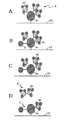
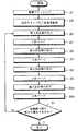
図1は、従来の原子層蒸着法を用いたアルミニウム酸化膜の形成過程を説明するためのフローチャートであり、図2Aないし図2Dは、図1に示したアルミニウム酸化膜の形成時の反応メカニズムを説明するために示す図である。 FIG. 1 is a flowchart for explaining a process of forming an aluminum oxide film using a conventional atomic layer deposition method. FIGS. 2A to 2D show a reaction mechanism at the time of forming the aluminum oxide film shown in FIG. It is a figure shown in order to demonstrate.
具体的には、まず、基板(S)の搬入された反応チャンバ(図示せず)に第1反応物(A)、すなわち、薄膜をなすアルミニウム(a1)とメチルリガンド(a2)よりなるトリメチルアルミニウム(Al(CH3)3、「TMA」と称する)を注入する(ステップ1)。Specifically, first, a reaction chamber (not shown) into which a substrate (S) is loaded is composed of a first reactant (A), that is, a thin film of aluminum (a1 ) and a methyl ligand (a2 ). Trimethylaluminum (Al (CH3 )3 , referred to as “TMA”) is injected (step 1).
次に、物理吸着されている第1反応物(A)を不活性ガスのパージにより除去する(ステップ3)。これにより、図2Aに示されたように、基板(S)上に第1反応物(A)が化学吸着される。 Next, the first reactant (A) that has been physically adsorbed is removed by purging with an inert gas (step 3). Thereby, as shown in FIG. 2A, the first reactant (A) is chemically adsorbed on the substrate (S).
次に、第1反応物(A)の化学吸着された反応チャンバに第2反応物(B)、すなわち、酸素(b1)と水素ラジカル(b2)よりなる水蒸気(H2O)を注入する(ステップ5)。これにより、図2Bに示されたように、第2反応物(B)が第1反応物(A)に化学吸着される。Next, the second reactant (B), that is, water vapor (H2 O) composed of oxygen (b1 ) and hydrogen radical (b2 ) is injected into the reaction chamber where the first reactant (A) is chemisorbed. (Step 5). Thereby, as shown in FIG. 2B, the second reactant (B) is chemisorbed onto the first reactant (A).
ここで、前記化学吸着された第2反応物(B)の水素ラジカル(b2)は、図2Cに示されたように、第1反応物(A)のメチルリガンド(a2)に移動して第1反応物(A)からメチルリガンドが分離される。すると、下記化学式(1)及び図2Dに示されたように、前記移動した第2反応物(B)の水素ラジカル(b2)が分離された第1反応物(A)のメチルリガンド(a2)と反応してCH4よりなる揮発性の気相物質(D)を形成する。そして、基板(S)上には第1反応物(A)のアルミニウム(a1)及び第2反応物(B)の酸素(b1)の反応によりアルミニウム酸化膜(C)が形成される。この反応を化学式で示すと、下記(1)式のとおりである。Here, the hydrogen radical (b2 ) of the chemisorbed second reactant (B) moves to the methyl ligand (a2 ) of the first reactant (A) as shown in FIG. 2C. Thus, the methyl ligand is separated from the first reactant (A). Then, as shown in the following chemical formula (1) and FIG. 2D, the methyl ligand (a) of the first reactant (A) from which the hydrogen radical (b2 ) of the transferred second reactant (B) was separated was separated.2 ) to form a volatile gas phase material (D) consisting of CH4 . An aluminum oxide film (C) is formed on the substrate (S) by the reaction of aluminum (a1 ) of the first reactant (A) and oxygen (b1 ) of the second reactant (B). This reaction is represented by the following chemical formula (1).
2Al(CH3)3+3H2O→Al2O3+6CH4 …(1)
次に、前記CH4よりなる揮発性の気相物質(D)と反応してない水蒸気は不活性ガスのパージによって除去する(ステップ7)。2Al (CH3 )3 + 3H2 O → Al2 O3 + 6CH4 (1)
Next, water vapor that has not reacted with the volatile gas phase substance (D) made of CH4 is removed by purging with an inert gas (step 7).
次に、前記形成されたアルミニウム酸化膜(C)の厚さが適宜であるかどうかを確認し(ステップ9)、必要ならば前記ステップ1からステップ7までの段階を周期的に繰り返し行う。 Next, it is confirmed whether or not the thickness of the formed aluminum oxide film (C) is appropriate (step 9). If necessary, the steps from
ところが、従来のALD法は、水素ラジカル(b2)の移動によってメチルリガンド(a2)が除去されるため、下記化学式2に示されたように、水素ラジカル(b2)の移動に応じて残存するOHラジカルによって副反応が発生する。この反応を化学式で示すと、下記(2)式のとおりである。However, in the conventional ALD method, since the methyl ligand (a2 ) is removed by the movement of the hydrogen radical (b2 ), as shown in the following
Al(CH3)3+3H2O→Al(OH)3+3CH4 …(2)
このように副反応が発生する場合、アルミニウム酸化膜(C)内に好ましくない不純物、例えば、Al(OH)3が含まれる。このようにAl(OH)3などの不純物が含まれると、所望の薄膜特性が得られなくなる。特に、含Al(OH)3の前記アルミニウム酸化膜を半導体素子の誘電膜に適用する場合電子のトラップサイトや電流リークサイトとして作用し、誘電膜の性質を低下させる結果となる。Al (CH3 )3 + 3H2 O → Al (OH)3 + 3CH4 (2)
Thus, when a side reaction occurs, an undesirable impurity, for example, Al (OH)3 is contained in the aluminum oxide film (C). When impurities such as Al (OH)3 are contained in this manner, desired thin film characteristics cannot be obtained. In particular, when the aluminum oxide film containing Al (OH)3 is applied to a dielectric film of a semiconductor element, it acts as an electron trap site or a current leak site, resulting in a deterioration in the properties of the dielectric film.
本発明は、上記事情に鑑みて成されたものであり、その目的は、原子層蒸着法を用いる場合に、好ましくない不純物の形成を抑止して化学量論に優れた薄膜が得られる薄膜形成方法を提供することである。 The present invention has been made in view of the above circumstances, and its purpose is to form a thin film having excellent stoichiometry by suppressing the formation of undesirable impurities when an atomic layer deposition method is used. Is to provide a method.
本発明による原子層蒸着法を用いた薄膜形成方法は、基板(S)上に第1反応物を化学吸着させた後、反応チャンバを不活性ガスでパージして物理吸着された第1反応物を除去する。次に、前記反応チャンバに水酸化基を含まない第2反応物を注入して前記化学吸着された第1反応物を金属−酸素原子層に置換させる。次に、前記反応チャンバを不活性ガスでパージして物理吸着された第2反応物を除去する。次に、前記反応チャンバに第3反応物を注入して前記化学吸着された第1反応物の残余分を金属−酸素原子層に置換させ、水酸化基の生成が抑止された状態で原子層単位の金属酸化膜を形成する。また、前記第3反応物の注入後に、不純物の除去及び化学量論の向上のための第4反応物、例えばオゾンガスを注入し、不活性ガスでパージすることもできる。 In the thin film formation method using the atomic layer deposition method according to the present invention, the first reactant is chemically adsorbed on the substrate (S) and then physically adsorbed by purging the reaction chamber with an inert gas. Remove. Next, a second reactant containing no hydroxyl group is injected into the reaction chamber to replace the chemisorbed first reactant with a metal-oxygen atomic layer. Next, the reaction chamber is purged with an inert gas to remove the physically adsorbed second reactant. Next, a third reactant is injected into the reaction chamber to replace the remainder of the chemisorbed first reactant with a metal-oxygen atomic layer, and in a state where generation of hydroxyl groups is suppressed, A unit metal oxide film is formed. In addition, after the third reactant is injected, a fourth reactant such as ozone gas for removing impurities and improving the stoichiometry can be injected and purged with an inert gas.
好ましくは、前記第1反応物としては金属反応物を用い、前記水酸化基を含まない第2反応物としてはN2O、O2、O3またはCO2を用い、前記第3反応物としては酸化ガスを用いる。また、好ましくは、前記第1反応物の注入段階から第3反応物の注入段階までの前記反応チャンバの温度は100〜400℃に保たれる。ここで、前記基板がシリコン基板である場合、前記第1反応物の注入前に酸化ガスを注入して基板の表面のダングリングボンドを終端処理することもできる。Preferably, a metal reactant is used as the first reactant, N2 O, O2 , O3 or CO2 is used as the second reactant not containing the hydroxyl group, and the third reactant is used as the third reactant. Uses oxidizing gas. Preferably, the temperature of the reaction chamber from the first reactant injection step to the third reactant injection step is maintained at 100 to 400 ° C. When the substrate is a silicon substrate, dangling bonds on the surface of the substrate may be terminated by injecting an oxidizing gas before injecting the first reactant.
また、本発明による原子層蒸着法を用いた薄膜形成方法は、基板(S)上に前記第1反応物を化学吸着させた後、反応チャンバを不活性ガスでパージして物理吸着された第1反応物を除去する。次に、前記反応チャンバに第2反応物を注入して第1反応物及び第2反応物の化学置換により原子層単位の薄膜を形成する。次に、前記反応チャンバを不活性ガスでパージして物理吸着された第2反応物を除去した後、前記薄膜の形成された反応チャンバに不純物の除去及び化学量論の向上のための第3反応物を注入する。 In addition, the thin film formation method using the atomic layer deposition method according to the present invention is a method in which the first reactant is chemically adsorbed on the substrate (S), and then the reaction chamber is purged with an inert gas and physically adsorbed. 1 Reactant is removed. Next, a second reactant is injected into the reaction chamber, and a thin film in units of atomic layers is formed by chemical replacement of the first reactant and the second reactant. Next, the reaction chamber is purged with an inert gas to remove the physically adsorbed second reactant, and then the reaction chamber in which the thin film is formed has a third structure for removing impurities and improving the stoichiometry. Inject the reactants.
好ましくは、前記第1反応物としては金属反応物を用い、第2及び第3反応物としては酸化ガスを用いる。また、好ましくは、前記第1反応物としては金属反応物を用い、第2及び第3反応物としては窒化ガスを用いる。ここで、前記基板がシリコン基板である場合、前記第1反応物の注入前に酸化ガスまたは窒化ガスをさらに注入して基板表面のダングリングボンドを終端処理することもできる。好ましくは、前記第1反応物の注入段階から第3反応物の注入段階までの前記反応チャンバの温度は100〜400℃に保たれる。 Preferably, a metal reactant is used as the first reactant, and an oxidizing gas is used as the second and third reactants. Preferably, a metal reactant is used as the first reactant, and a nitriding gas is used as the second and third reactants. Here, when the substrate is a silicon substrate, dangling bonds on the substrate surface can be terminated by further injecting an oxidizing gas or a nitriding gas before the first reactant is injected. Preferably, the temperature of the reaction chamber from the first reactant injection step to the third reactant injection step is maintained at 100-400 ° C.
本発明によると、水酸化基などの好ましくない副産物の生成を防止ないし抑止して不純物を含むことなく、かつ化学量論に優れた薄膜を得ることができる。 According to the present invention, it is possible to obtain a thin film excellent in stoichiometry without containing impurities by preventing or inhibiting formation of undesirable by-products such as hydroxyl groups.
本発明による原子層蒸着法を用いた薄膜形成方法によれば、原子層蒸着法を用いて金属酸化膜を形成するときに、第1反応物を水酸化基を含んでいない第2反応物とあらかじめ反応させて第1反応物の絶対量を減らした後に、第1反応物と水酸化基を含んでいる第3反応物とを再び反応させることにより、金属酸化膜内に水酸化基などの副産物の生成を抑止させることができる。例えば、本発明は、トリメチルアルミニウムを、水酸化基を含んでいないN2Oとあらかじめ反応させてトリメチルアルミニウムの絶対量を減らした後に再び水蒸気と反応させることで、水酸化基の絶対量が少ない状態でアルミニウム酸化膜を形成することができる。According to the thin film formation method using the atomic layer deposition method according to the present invention, when the metal oxide film is formed using the atomic layer deposition method, the first reactant is converted to the second reactant containing no hydroxyl group. After reducing the absolute amount of the first reactant by reacting in advance, the first reactant and the third reactant containing a hydroxyl group are reacted again, so that a hydroxyl group or the like is contained in the metal oxide film. Generation of by-products can be suppressed. For example, in the present invention, trimethylaluminum is reacted with N2 O not containing a hydroxyl group in advance to reduce the absolute amount of trimethylaluminum, and then reacted again with water vapor, thereby reducing the absolute amount of hydroxyl groups. An aluminum oxide film can be formed in the state.
また、本発明による原子層蒸着法を用いた薄膜形成方法によれば、原子層蒸着法を用いる時に反応チャンバに薄膜を形成する薄膜形成用第1反応物及び第2反応物のほかに、不純物の除去及び化学量論の向上のための第3反応物を注入及びパージする。これにより、不純物が含まれていず、しかも化学量論に優れた薄膜を得ることができる。 Further, according to the thin film forming method using the atomic layer deposition method according to the present invention, in addition to the first reactant and the second reactant for forming a thin film in the reaction chamber when the atomic layer deposition method is used, impurities The third reactant is injected and purged for removal of and increasing stoichiometry. Thereby, it is possible to obtain a thin film which does not contain impurities and is excellent in stoichiometry.
以下、添付した図面に基づき、本発明の実施の形態について詳細に説明する。しかし、後述する本発明の実施の形態は各種の形態に変形でき、本発明の範囲が後述する実施の形態に限定されることはない。本発明の実施の形態は当業界における通常の知識を有した者に本発明をより完全に説明するために提供されるものである。なお、図中、膜または領域の大きさまたは厚さは明細書の明確性のために誇張されている。また、ある膜が他の膜または基板の「上」にあると記載されている場合、前記ある膜が前記他の膜の上に直接的に存在することもできれば、その間に第3の膜を介在されることもできる。 Hereinafter, embodiments of the present invention will be described in detail with reference to the accompanying drawings. However, the embodiment of the present invention described later can be modified into various forms, and the scope of the present invention is not limited to the embodiment described later. Rather, these embodiments are provided so that this disclosure will be thorough and complete, and will fully convey the concept of the invention to those skilled in the art. In the drawings, the size or thickness of the film or region is exaggerated for clarity of the specification. Also, when it is described that a certain film is “on” another film or substrate, the certain film can be directly present on the other film. It can also be interposed.
図3は、本発明の原子層蒸着法を用いた薄膜形成方法に用いられる原子層薄膜形成装置を説明するための概略図である。 FIG. 3 is a schematic view for explaining an atomic layer thin film forming apparatus used in the thin film forming method using the atomic layer deposition method of the present invention.
この原子層薄膜形成装置は、外部のヒーター(図示せず)により加熱される反応チャンバ11と、基板15、例えばシリコン基板が置かれるように前記反応チャンバ11の底面に設けられたサセプタ13と、反応ガスが前記反応チャンバ11の内部に注入されるように前記サセプタ13の上部に設けられたシャワーヘッド17と、前記反応チャンバ11の内部の圧力を調節するために前記反応チャンバ11と連結された真空ポンプ19とを具備する。 This atomic layer thin film forming apparatus includes a
前記シャワーヘッド17には、互いに別々の2本のガス注入管A及びBが連結されている。そして、このシャワーヘッド17には、第1反応物、不活性ガス、第2反応物及び第3反応物が注入される。第1反応物は金属反応物であり、不活性ガスは窒素ガスやアルゴンガスであり、第2反応物は水酸化基を含んでいない酸化ガス、例えばN2O、O2、O3またはCO2ガス、または水蒸気であり、第3反応物は水蒸気や活性化した酸化剤であって、酸素ラジカルを含んでいる物質、例えば、オゾン、プラズマO2、プラズマN2Oである。図3において、便宜上第2反応物及び第3反応物を別々に構成したが、単一に構成しても良い。Two separate gas injection pipes A and B are connected to the
そして、第1反応物及び不活性ガスは、前記ガス注入管Aを通じて反応チャンバ11の内部に注入され、第2反応物及び第3反応物は、前記ガス注入管Bを通じて反応チャンバ11の内部に注入される。ここで、前記第1反応物と第2反応物及び第3反応物のガス管を別々にしたのは、単一のガス管(AまたはB)内での反応物間の反応を抑止するためである。 The first reactant and the inert gas are injected into the
前記第1反応物及び前記不活性ガスは、各々第1弁V1及び第2弁V2により反応チャンバ11の内部への注入が制御され、前記第2反応物及び第3反応物は各々第3弁V3、第4弁V4によって前記反応チャンバ11の内部への注入が制御される。 Injection of the first reactant and the inert gas into the
以下、図3の原子層薄膜形成装置を用いた薄膜形成方法の各種の実施の形態について説明する。 Hereinafter, various embodiments of the thin film forming method using the atomic layer thin film forming apparatus of FIG. 3 will be described.
第1の実施の形態
図4Aないし図4Dは、本発明を適用した第1の実施の形態による原子層蒸着法を用いた薄膜形成方法の反応メカニズムを説明するための図面である。First Embodiment FIGS. 4A to 4D are diagrams for explaining a reaction mechanism of a thin film forming method using an atomic layer deposition method according to a first embodiment to which the present invention is applied.
まず、基板(図3の15)、例えばシリコン基板の搬入された反応チャンバ11に、薄膜をなす元素(a1)とリガンド(a2)よりなる第1反応物(A)を注入して基板15上に第1反応物(A)を化学吸着させた後、物理吸着されている第1反応物(A)を不活性ガスのパージにより除去する(図4A参照)。First, a first reactant (A) composed of a thin film element (a1 ) and a ligand (a2 ) is injected into a
次に、第1反応物(A)の吸着された反応チャンバ11に第2反応物(B)を注入する。これにより、第2反応物(B)は第1反応物(A)に化学吸着される。ここで、前記第2反応物(B)としては、第1反応物(A)との反応性が大きい不完全な物質を用いる。そして、第2反応物(B)としては、前記第2反応物(B)と第1反応物(A)の薄膜をなす元素(a1)との結合エネルギーが前記第1反応物(A)の薄膜をなす元素(a1)とリガンド(a2)との結合エネルギーよりも大きい物質を用いる(図4B参照)。Next, the second reactant (B) is injected into the
図4Cを参照すれば、前記第2反応物(B)と第1反応物(A)の薄膜をなす元素(a1)との結合エネルギーが前記第1反応物(A)の薄膜をなす元素(a1)とリガンド(a2)との結合エネルギーよりも大きいため、第2反応物(B)は第1反応物(A)の薄膜をなす元素(a1)と結合しようとし、かつ第1反応物(A)からリガンド(a2)は分離される。Referring to FIG. 4C, the binding energy of the second reactant (B) and the element (a1 ) forming the thin film of the first reactant (A) is the element forming the thin film of the first reactant (A). Since the binding energy of (a1 ) and the ligand (a2 ) is larger, the second reactant (B) tries to bind to the element (a1 ) forming the thin film of the first reactant (A), and Ligand (a2 ) is separated from one reactant (A).
次に、前記第1反応物(A)から分離されたリガンド(a2)は不安定な状態であるため、リガンド(a2)間の結合によって揮発性の気相物質(D)を形成する。そして、基板15上には第1反応物(A)の薄膜をなす元素(a1)及び第2反応物(B)の反応によって原子層単位の薄膜(C)が形成される。前記揮発性の気相物質(D)は不活性ガスのパージによって除去される(図4D参照)。Next, since the ligand (a2 ) separated from the first reactant (A) is in an unstable state, a volatile gas phase substance (D) is formed by bonding between the ligands (a2 ). . A thin film (C) in atomic layer units is formed on the
次に、図4Aないし図4Dに示された結合エネルギーの違いを用いた薄膜形成方法をアルミニウム酸化膜の形成過程に適用した場合を例にとって説明する。 Next, a case where the thin film formation method using the difference in binding energy shown in FIGS. 4A to 4D is applied to the formation process of the aluminum oxide film will be described as an example.
図5は、前記第1の実施の形態によるアルミニウム酸化膜の形成過程を説明するためのフローチャートであり、図6Aないし図6Dは、図5の原子層蒸着法を用いてアルミニウム酸化膜を形成するときの反応メカニズムを説明するための図面である。 FIG. 5 is a flowchart for explaining the formation process of the aluminum oxide film according to the first embodiment. FIGS. 6A to 6D form the aluminum oxide film using the atomic layer deposition method of FIG. It is drawing for demonstrating the reaction mechanism at the time.
まず、基板(図3の15)、例えばシリコン基板の搬入された反応チャンバ11に、第1反応物として薄膜をなすアルミニウム(a1)とメチルリガンド(a2)よりなるトリメチルアルミニウム(Al(CH3)3、TMA:「A」)を注入する(ステップ101)。次に、物理吸着されているTMAを不活性ガスで1次パージして除去する(ステップ103)。これにより、図6Aに示されたように、基板15上にTMAが化学吸着される。First, trimethylaluminum (Al (CH) made of aluminum (a1 ) and methyl ligand (a2 ) forming a thin film as a first reactant in a
次に、TMAの吸着された反応チャンバ11に、第2反応物として活性化した酸化剤であるオゾン(B)を注入する(ステップ105)。これにより、オゾン(B)は、図6Bに示されたように、TMAのアルミニウム(a1)に化学吸着される。Next, ozone (B), which is an oxidant activated as the second reactant, is injected into the
ここで、前記オゾン(B)は、TMAとの反応性が大きく、かつ不完全な物質である。そして、前記オゾン(B)はTMAのアルミニウム(a1)との結合エネルギーが約540kJ/molであって、前記TMAのアルミニウム(a1)とメチルリガンド(a2)との結合エネルギー(例えば、Al−C結合エネルギー)である255kJ/molよりも大きい物質である。前記オゾン(B)とTMAの薄膜をなす元素であるアルミニウム(a1)との結合エネルギーが前記TMAの薄膜をなす元素であるアルミニウム(a1)とメチルリガンド(a2)との結合エネルギーよりも大きいため、図6Cに示されたように、TMAからメチルリガンド(a2)が分離される。Here, the ozone (B) is an incomplete substance having high reactivity with TMA. The ozone (B) has a binding energy of about 540 kJ / mol with the aluminum (a1 ) of TMA, and the binding energy of the aluminum (a1 ) of the TMA with the methyl ligand (a2 ) (for example, Al—C bond energy) which is greater than 255 kJ / mol. Than the binding energy between the ozone (B) and aluminum is an element which forms a thin film of TMA aluminum (a1) binding energy that it is an element which forms a thin film of the TMA (a1) and methyl ligand (a2) Therefore, methyl ligand (a2 ) is separated from TMA as shown in FIG. 6C.
また、前記TMAから分離されたメチルリガンド(a2)は不安定な状態であるため、図6Dに示されたように、メチルリガンド(a2)間の結合によってC2H6よりなる揮発性の気相物質(D)を形成する。そして、基板15上にはTMAの薄膜をなすアルミニウム(a1)とオゾン(B)との反応によって、下記化学式(3)に示されたように原子層単位のアルミニウム酸化膜(C)が形成される。Further, since the methyl ligand (a2 ) separated from the TMA is in an unstable state, as shown in FIG. 6D, the volatility of C2 H6 is caused by the bond between the methyl ligands (a2 ). The gas phase material (D) is formed. Then, an aluminum oxide film (C) in atomic layer units is formed on the
2Al(CH3)3+O3→Al2O3+3C2H6 …(3)
次に、前記反応チャンバを不活性ガスで2次パージして前記C2H6の揮発性の気相物質(D)と反応してないメチルリガンド(a2)を除去する(ステップ107)。続いて、前記形成されたアルミニウム酸化膜の厚さが適宜であるかどうかを確認し(ステップ109)、必要ならば前記ステップ101からステップ107までの段階を周期的に繰り返し行う。2Al (CH3 )3 + O3 → Al2 O3 + 3C2 H6 (3)
Next, the reaction chamber is secondarily purged with an inert gas to remove methyl ligand (a2 ) that has not reacted with the volatile gas phase substance (D) of C2 H6 (step 107). Subsequently, it is confirmed whether or not the thickness of the formed aluminum oxide film is appropriate (step 109). If necessary, the steps from
この実施の形態では、第2反応物としてオゾンを使用したが、紫外線を使ってオゾンをさらに活性化させることもできる。また、前記活性化した酸化剤として、オゾンに代えて、下記化学式(4)に示されたように、プラズマO2やプラズマN2Oを使用することもできる。
TMA+O2(activated)⇒4Al(CH3)3+3O2
→Al2O3+6C2H6 …(4)
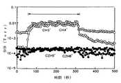
図7及び図8は各々、従来の技術及び本発明の第1の実施の形態によってアルミニウム酸化膜を形成するときのRGA(Residual gas analysis)データを示すグラフである。図7及び図8において、矢印で表示された区間がアルミニウム酸化膜が形成される区間である。In this embodiment, ozone is used as the second reactant, but ozone can be further activated using ultraviolet rays. Further, as the activated oxidizing agent, plasma O2 or plasma N2 O can be used as shown in the following chemical formula (4), instead of ozone.
TMA + O2 (activated) ⇒4Al (CH3 )3 + 3O2
→ Al2 O3 + 6C2 H6 (4)
7 and 8 are graphs showing RGA (Residual gas analysis) data when forming an aluminum oxide film according to the conventional technique and the first embodiment of the present invention, respectively. 7 and 8, a section indicated by an arrow is a section where an aluminum oxide film is formed.
前述したように、第2反応物(B)と第1反応物(A)との反応メカニズムに応じて除去されるリガンドの形態が異なるため、工程中に発生する物質も異なってくる。すなわち、従来は、図7のように、第1反応物(A)としてTMAを、そして第2反応物(B)として水蒸気(H2O)を使用する場合には、水蒸気から水素ラジカルを受けて生成されたCH3+、CH4+が主な副産物として検出される。これに対し、本発明による第1の実施の形態により、図8のように、第1反応物(A)としてTMAを、そして第2反応物(B)としてオゾンを使用する場合にはCH3リガンドが除去されて、C2H5+やC2H6+が副産物として検出されることが分かる。As described above, since the form of the ligand to be removed differs depending on the reaction mechanism between the second reactant (B) and the first reactant (A), the substances generated during the process also differ. That is, conventionally, as shown in FIG. 7, when TMA is used as the first reactant (A) and water vapor (H2 O) is used as the second reactant (B), hydrogen radicals are received from the water vapor. CH3+ and CH4+ produced in this manner are detected as main by-products. In contrast, according to the first embodiment of the present invention, as shown in FIG. 8, when TMA is used as the first reactant (A) and ozone is used as the second reactant (B), CH3 It can be seen that the ligand is removed and C2 H5+ and C2 H6+ are detected as by-products.
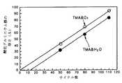
図9は、従来の技術及び本発明の第1の実施の形態によりアルミニウム酸化膜を形成する場合におけるサイクル数によるアルミニウム酸化膜の厚さを示すグラフである。 FIG. 9 is a graph showing the thickness of the aluminum oxide film according to the number of cycles when the aluminum oxide film is formed according to the conventional technique and the first embodiment of the present invention.
原子層蒸着法は、表面調節工程であるため、各反応物の供給サイクル数により蒸着される薄膜の厚さが決定される。すなわち、サイクルに応じて線形的に厚さが増大するなら、原子層蒸着法により薄膜が形成されるということを意味する。図9に示されたように、従来及び本発明共に線形的に厚さが増大するため、原子層蒸着法を用いて薄膜が形成されるということが分かる。 Since the atomic layer deposition method is a surface conditioning step, the thickness of the deposited thin film is determined by the number of supply cycles of each reactant. That is, if the thickness increases linearly according to the cycle, it means that a thin film is formed by atomic layer deposition. As shown in FIG. 9, since the thickness increases linearly in both the conventional and the present invention, it can be seen that the thin film is formed using the atomic layer deposition method.
ところが、第2反応物(B)として水蒸気を用いる従来技術(●にて表示)とオゾンを用いる本発明(○にて表示)との間には、潜伏サイクルの違いが見られる。すなわち、本発明では潜伏サイクルなしに初期サイクルから蒸着がなされるのに対し、従来技術では12サイクルの潜伏期間が経過してから薄膜が蒸着される。このことは、初期界面が異質的な反応によって形成されるので、本発明の場合がより安定的にアルミニウム酸化膜が形成されるということを意味する。 However, there is a difference in the latent cycle between the prior art using water vapor as the second reactant (B) (indicated by ●) and the present invention using ozone (indicated by ○). That is, in the present invention, the deposition is performed from the initial cycle without the latent cycle, whereas in the conventional technique, the thin film is deposited after the 12-cycle latent period has elapsed. This means that the aluminum oxide film is more stably formed in the case of the present invention because the initial interface is formed by a heterogeneous reaction.
図10は、従来及び本発明の第1の実施の形態によって形成されたアルミニウム酸化膜の温度によるストレス履歴を示すグラフである。 FIG. 10 is a graph showing the stress history depending on the temperature of the aluminum oxide film formed according to the prior art and the first embodiment of the present invention.
第1反応物(A)としてTMAを、そして第2反応物(B)として水蒸気を用いて形成された従来のアルミニウム酸化膜のストレス履歴(□にて表示)は、ストレスの形態が450℃で引張ストレスから圧縮ストレスに変わる。これに対し、第1反応物AとしてTMAを、そして第2反応物(B)としてオゾンを用いて形成された本発明のアルミニウム酸化膜のストレス履歴(●にて表示)は、全温度範囲に亘って引張ストレスにストレスモードが変わらないため、膜そのものが熱に対してより安定的であることが分かる。 The stress history (indicated by □) of the conventional aluminum oxide film formed using TMA as the first reactant (A) and water vapor as the second reactant (B) shows that the stress form is 450 ° C. Changes from tensile stress to compressive stress. In contrast, the stress history (indicated by ●) of the aluminum oxide film of the present invention formed using TMA as the first reactant A and ozone as the second reactant (B) is in the entire temperature range. Since the stress mode does not change over the tensile stress, it can be seen that the film itself is more stable against heat.
図11は、従来の技術及び本発明の第1実施の形態によって形成されたアルミニウム酸化膜の後アニーリング条件による厚さ収縮率を示すグラフである。 FIG. 11 is a graph showing the thickness shrinkage rate according to the post-annealing condition of the aluminum oxide film formed according to the conventional technique and the first embodiment of the present invention.
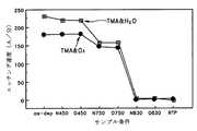
図11のX軸においてN450、N750、N830は各々450℃、750℃、830℃の窒素雰囲気下で後アニーリングを行ったサンプルであり、O450、O750、O830は各々450℃、750℃、830℃の酸素雰囲気下で後アニーリングを行ったサンプルであり、RTOは850℃で急速熱酸化させたサンプルである。従来の技術及び本発明の第1実施の形態によって形成されたアルミニウム酸化膜は、後アニーリングの温度及びガス条件によって厚さ収縮率(厚さ減少率)が大きく変わらないことが分かる。 In the X axis of FIG. 11, N450, N750, and N830 are samples subjected to post-annealing in nitrogen atmospheres of 450 ° C., 750 ° C., and 830 ° C., and O450, O750, and O830 are 450 ° C., 750 ° C., and 830 ° C., respectively. The sample was subjected to post-annealing in an oxygen atmosphere, and the RTO was a sample rapidly oxidized at 850 ° C. It can be seen that the thickness shrinkage rate (thickness reduction rate) of the aluminum oxide film formed according to the conventional technique and the first embodiment of the present invention does not vary greatly depending on the post-annealing temperature and gas conditions.
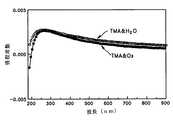
図12及び図13は各々、従来の技術及び本発明の第1実施の形態によって形成されたアルミニウム酸化膜の波長による吸収常数及び屈折率を示すグラフである。 12 and 13 are graphs showing the absorption constant and the refractive index according to the wavelength of the aluminum oxide film formed according to the conventional technique and the first embodiment of the present invention, respectively.
従来の技術及び本発明の第1実施の形態によって形成されたアルミニウム酸化膜は、図12に示されたように、180〜900nmの広い波長帯で吸収常数が0.005以下の値を有する優れた透明度を表す。そして、従来の技術及び本発明の第1実施の形態によって形成されたアルミニウム酸化膜の屈折率は、図13に示されたように、180〜900nmの広い波長帯で大きく変わらないことが分かる。 The aluminum oxide film formed by the conventional technique and the first embodiment of the present invention has an excellent absorption constant of 0.005 or less in a wide wavelength band of 180 to 900 nm as shown in FIG. Represents transparency. Then, it can be seen that the refractive index of the aluminum oxide film formed by the conventional technique and the first embodiment of the present invention does not change greatly in a wide wavelength band of 180 to 900 nm as shown in FIG.
図14は、従来の技術及び本発明の第1実施の形態によって形成されたアルミニウム酸化膜の後アニーリング温度及び雰囲気ガスによる湿式エッチング速度を各々示すグラフである。 FIG. 14 is a graph showing the post-annealing temperature of the aluminum oxide film formed according to the conventional technique and the first embodiment of the present invention, and the wet etching rate by the atmospheric gas.
図14のX軸において、「as−dep」は基板上に蒸着した後にアニーリングしていないサンプルであり、N450、N750、N830は各々450℃、750℃、830℃の窒素雰囲気下で後アニーリングを行なったサンプルである。また、O450、O750、O830は各々450℃、750℃、830℃の酸素雰囲気下で後アニーリングを行ったサンプルであり、RTPは850℃の酸素雰囲気下で急速熱酸化させたサンプルである。そして、Y軸は、各々のサンプルに対して200:1のHF溶液で湿式エッチングを行ったときのエッチング速度を表す。 In the X-axis of FIG. 14, “as-dep” is a sample that has not been annealed after being deposited on the substrate, and N450, N750, and N830 are post-annealed in nitrogen atmospheres of 450 ° C., 750 ° C., and 830 ° C., respectively. It is the sample which was done. O450, O750, and O830 are samples that are post-annealed in an oxygen atmosphere of 450 ° C., 750 ° C., and 830 ° C., respectively, and RTP is a sample that is rapidly thermally oxidized in an oxygen atmosphere of 850 ° C. The Y axis represents the etching rate when wet etching is performed on each sample with a 200: 1 HF solution.
図14に示されたように、従来の技術及び本発明の第1実施の形態によって形成されたアルミニウム酸化膜は、アニーリング条件に無関係にアニーリング温度が増大するに従って湿式エッチング速度が落ちる。特に、800℃以上で後アニーリングを行えば、エッチング速度が2〜3Å/minに急減する。また、800℃以下で後アニーリングを行えば、本発明の第1の実施の形態によるアルミニウム酸化膜のエッチング速度が従来に比べて約30%小さくなることが分かる。これより、オゾンを酸化ガスとして用いる場合がH2Oを酸化ガスとして用いる場合よりも化学的に安定していることが分かる。As shown in FIG. 14, the wet etching rate of the aluminum oxide film formed by the conventional technique and the first embodiment of the present invention decreases as the annealing temperature increases regardless of the annealing conditions. In particular, if post-annealing is performed at 800 ° C. or higher, the etching rate is rapidly reduced to 2 to 3 mm / min. It can also be seen that if post-annealing is performed at 800 ° C. or lower, the etching rate of the aluminum oxide film according to the first embodiment of the present invention is reduced by about 30% compared to the conventional case. This shows that the case where ozone is used as the oxidizing gas is chemically more stable than the case where H2 O is used as the oxidizing gas.
以下、本発明の第1の実施の形態によって形成されたアルミニウム酸化膜を半導体素子に採用した場合について説明する。 Hereinafter, a case where the aluminum oxide film formed according to the first embodiment of the present invention is employed in a semiconductor element will be described.
図15は、本発明の第1の実施の形態によって形成された誘電膜が採用された半導体素子のキャパシタ構造を示す断面図である。 FIG. 15 is a cross-sectional view showing a capacitor structure of a semiconductor device employing a dielectric film formed according to the first embodiment of the present invention.
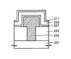
本発明の第1の実施の形態によって形成された誘電膜が採用された半導体素子のキャパシタは、基板201、例えばシリコン基板上に形成された下部電極205、誘電膜207及び上部電極209を含む。図15中、参照番号203は層間絶縁膜であり、参照番号211はキャパシタの上部電極上に形成されるキャッピング膜である。 The capacitor of the semiconductor device employing the dielectric film formed according to the first embodiment of the present invention includes a
以下、前記上部電極209及び下部電極205の両方を不純物のドーピングされたポリシリコン膜で構成し、かつ誘電膜207を本発明の第1の実施の形態によって形成されたアルミニウム酸化膜で構成したキャパシタを「SISキャパシタ」と呼ぶ。そして、前記下部電極205を不純物のドーピングされたポリシリコン膜で構成し、誘電膜207を本発明の第1の実施の形態によって形成されたアルミニウム酸化膜で構成し、上部電極209はTiN膜で構成した場合を「MISキャパシタ」と呼ぶ。また、前記上部電極209及び下部電極205の両方を白金族貴金属膜、例えばPt、Ru等で構成し、誘電膜207を絶縁膜、例えばタンタル酸化膜やBST(BaSrTiO3)膜で構成したキャパシタを「MIMキャパシタ」と呼ぶ。Hereinafter, a capacitor in which both the
図16は、本発明の第1の実施の形態によって形成された誘電膜が採用された半導体素子のトランジスタ構造を示す断面図である。 FIG. 16 is a cross-sectional view showing a transistor structure of a semiconductor device employing a dielectric film formed according to the first embodiment of the present invention.
本発明の第1の実施の形態による誘電膜が採用された半導体素子は、第1電極としてリン、ひ素、ボロン、フッ素などの不純物がドーピングされたシリコン基板301と、誘電膜としてゲート絶縁膜305と、第2電極としてゲート電極307とを具備する。図16中、参照番号303は不純物ドーピング領域であって、ソースまたはドレイン領域を表す。 The semiconductor device employing the dielectric film according to the first embodiment of the present invention includes a
ここで、本発明の半導体素子のトランジスタ構造は、キャパシタ構造と比較するとき、シリコン基板301は下部電極に対応し、ゲート電極307は上部電極に対応する。また、前記ゲート絶縁膜305はキャパシタの誘電膜に対応する。 Here, in the transistor structure of the semiconductor element of the present invention, the
次に、説明の便宜上キャパシタ構造を参照して誘電膜の絶縁特性を説明するが、トランジスタ構造でも同一に適用できる。 Next, the insulating characteristics of the dielectric film will be described with reference to the capacitor structure for convenience of description, but the same applies to the transistor structure.
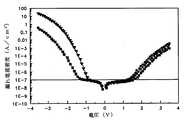
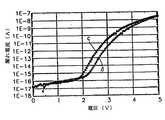
図17は、従来のキャパシタ及び本発明の第1の実施の形態によって形成された誘電膜が採用されたSISキャパシタの印加電圧による漏れ電流特性を説明するために示すグラフである。 FIG. 17 is a graph for explaining the leakage current characteristics depending on the applied voltage of the SIS capacitor employing the conventional capacitor and the dielectric film formed according to the first embodiment of the present invention.
本発明のSISキャパシタ(○にて表示)は、従来のキャパシタ(●にて表示)と比較して、誘電膜の形成方法を異ならしめたことを除いては同一に構成した。図17に示されたように、一般的な半導体素子のキャパシタで許容可能な漏れ電流密度である1E−7A/cm2において、本発明のSISキャパシタは従来のキャパシタよりも約0.4Vだけ印加電圧を大きくできることが分かる。したがって、本発明のSISキャパシタは一定の漏れ電流値で誘電膜の厚さをより低くでき、半導体素子の集積化に有利である。なお、漏れ電流密度「1E−7」などは、「1×10−7」などを示すものである。これは本明細書および図面において同様である。The SIS capacitor of the present invention (indicated by a circle) is identical in structure to the conventional capacitor (indicated by a circle) except that the method for forming the dielectric film is different. As shown in FIG. 17, at 1E-7 A / cm2 , which is an allowable leakage current density in a capacitor of a general semiconductor device, the SIS capacitor of the present invention applies about 0.4 V more than the conventional capacitor. It can be seen that the voltage can be increased. Therefore, the SIS capacitor of the present invention can reduce the thickness of the dielectric film with a constant leakage current value, which is advantageous for integration of semiconductor devices. The leakage current density “1E-7” or the like indicates “1 × 10⁻⁷ ” or the like. This is the same in the present specification and drawings.
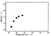
図18は、本発明の第1実施の形態によって形成された誘電膜が採用されたSISキャパシタの等価酸化膜によるリーク電流密度が1E−7A/cm2以上になる絶縁特性を示す離陸電圧のグラフである。なお、離陸電圧とは前記図17のように、低部傾斜が急激に変わるような特性を示す電圧のことである。FIG. 18 is a graph of take-off voltage showing an insulation characteristic in which the leakage current density by the equivalent oxide film of the SIS capacitor employing the dielectric film formed according to the first embodiment of the present invention is 1E-7 A / cm2 or more. It is. The take-off voltage is a voltage that exhibits characteristics such that the low slope changes rapidly as shown in FIG.
図18に示したように、本発明によるSISキャパシタは、等価酸化膜の厚さが35Åまでは安定的な絶縁特性を示すため、離陸電圧があまり減少しない。そして、等価酸化膜の厚さが35Å以下になると、離陸電圧が急減されて絶縁特性が弱くなる。 As shown in FIG. 18, the SIS capacitor according to the present invention exhibits stable insulation characteristics until the equivalent oxide film thickness is up to 35 mm, so that the take-off voltage does not decrease so much. When the thickness of the equivalent oxide film is 35 mm or less, the take-off voltage is sharply reduced and the insulation characteristics are weakened.
図19は、本発明の第1の実施の形態によって形成された誘電膜が採用されたMISキャパシタの印加電圧による漏れ電流特性を示すグラフである。 FIG. 19 is a graph showing the leakage current characteristics depending on the applied voltage of the MIS capacitor employing the dielectric film formed according to the first embodiment of the present invention.
漏れ電流密度が1E−7A/cm2であり、電圧が1.2Vである一般的な基準値で、本発明のMISキャパシタの場合、等価酸化膜の厚さを26.5Åにすることができる。このように等価酸化膜の厚さを低くする場合、半導体素子の集積化に極めて有利である。In the case of the MIS capacitor of the present invention, the thickness of the equivalent oxide film can be made 26.5 mm with a general reference value in which the leakage current density is 1E-7 A / cm2 and the voltage is 1.2 V. . Thus, reducing the thickness of the equivalent oxide film is extremely advantageous for integration of semiconductor elements.
図20は、本発明の第1の実施の形態によって形成された誘電膜が採用されたMISキャパシタ及び従来のキャパシタの漏れ電流特性を比較したグラフである。 FIG. 20 is a graph comparing the leakage current characteristics of a MIS capacitor employing a dielectric film formed according to the first embodiment of the present invention and a conventional capacitor.
従来のキャパシタは、本発明のMISキャパシタと比較して、誘電膜を除いては同一である。図20に示されたように、本発明の第1の実施の形態によって形成されたアルミニウム酸化膜を採用したMISキャパシタは、セル当たり1fAの漏れ電流値で誘電膜としてタンタル酸化膜(TaO)や窒化膜−酸化膜(NO)を使用した従来のキャパシタと比較してみるとき、印加電圧がもっとも大きい。換言すれば、本発明のMISキャパシタは従来のキャパシタと比較してみるとき、薄い等価酸化膜でも最高の漏れ電流特性を有することができる。図20において、括弧内の数字は誘電膜の厚さを表わす。 The conventional capacitor is the same as the MIS capacitor of the present invention except for the dielectric film. As shown in FIG. 20, the MIS capacitor employing the aluminum oxide film formed according to the first embodiment of the present invention has a leakage current value of 1 fA per cell and a tantalum oxide film (TaO) as a dielectric film. When compared with a conventional capacitor using a nitride film-oxide film (NO), the applied voltage is the highest. In other words, when compared with the conventional capacitor, the MIS capacitor of the present invention can have the best leakage current characteristics even with a thin equivalent oxide film. In FIG. 20, the numbers in parentheses represent the thickness of the dielectric film.
図21及び図22は各々、従来の技術及び本発明の第1の実施の形態によるアルミニウム酸化膜をMIMキャパシタのキャッピング膜として採用する場合の印加電圧による漏れ電流特性を示すグラフである。 FIGS. 21 and 22 are graphs showing leakage current characteristics depending on applied voltage when the aluminum oxide film according to the conventional technique and the first embodiment of the present invention is used as the capping film of the MIM capacitor, respectively.
図21及び図22において、「黒四角」はキャッピング膜を採用していない場合のMIMキャパシタを表す。図21において、「●」は従来の技術によりキャッピング膜としてアルミニウム酸化膜を形成した場合であり、「黒下三角」はアルミニウム酸化膜をキャッピング膜として形成した後、400℃で水素アニーリングを行なった場合を表わす。図22において、「●」は本発明の第1の実施の形態によってキャッピング膜としてアルミニウム酸化膜を形成した場合であり、「黒上三角」はアルミニウム酸化膜をキャッピング膜として形成した後400℃で水素アニーリングを行った場合であり、「黒下三角」はアルミニウム酸化膜をキャッピング膜として形成した後700℃で窒素アニーリングを行った場合である。 21 and 22, “black squares” represent MIM capacitors when a capping film is not employed. In FIG. 21, “●” indicates a case where an aluminum oxide film is formed as a capping film by a conventional technique, and “black lower triangle” indicates hydrogen annealing at 400 ° C. after the aluminum oxide film is formed as a capping film. Represents a case. In FIG. 22, “●” indicates a case where an aluminum oxide film is formed as a capping film according to the first embodiment of the present invention, and “black upper triangle” indicates that the aluminum oxide film is formed as a capping film at 400 ° C. This is a case where hydrogen annealing is performed, and a “black lower triangle” is a case where nitrogen annealing is performed at 700 ° C. after forming an aluminum oxide film as a capping film.
一般的に、半導体素子においてMIMキャパシタを採用する場合、後続するアロイ工程で用いられる水素アニーリング時に誘電膜が劣化する問題がある。このため、MIMキャパシタ上には水素バリアーの役目をするキャッピング膜を形成する。ところが、図21に示されたように、本発明の第1の実施の形態によって形成されたアルミニウム酸化膜をキャッピング膜として採用すれば、漏れ電流密度1E−7A/cm2の基準からみるとき、アルミニウム酸化膜をキャッピング膜として形成した場合だけでなく、後続する水素アニーリングによってもバリアー特性に極めて優れているので、漏れ電流特性を劣化させない。しかし、図22に示されたように、従来の技術によって形成されたアルミニウム酸化膜をキャッピング膜として採用すれば、蒸着中に水蒸気の水素及びOHリガンドがMIMキャパシタの漏れ電流特性を劣化させる。In general, when a MIM capacitor is employed in a semiconductor device, there is a problem that a dielectric film deteriorates during hydrogen annealing used in a subsequent alloy process. For this reason, a capping film serving as a hydrogen barrier is formed on the MIM capacitor. However, as shown in FIG. 21, if the aluminum oxide film formed according to the first embodiment of the present invention is used as a capping film, when viewed from the standard of leakage
第2の実施の形態
図23は、本発明の原子層蒸着法を用いた薄膜形成方法の第2の実施の形態を説明するために示すフローチャートである。Second Embodiment FIG. 23 is a flowchart shown for explaining a second embodiment of a thin film forming method using the atomic layer deposition method of the present invention.
基板15(図3参照)、例えばシリコン基板を酸化ガスにより酸素フラッシングして基板15のダングリングボンドを酸素と結合させる終端処理を行う(ステップ21)。前記酸素フラッシング以外にも、オゾン洗浄及びシリコン酸化膜の形成などの方法によってもダングリングボンドを酸素と結合させることができる。また、必要に応じて、前記基板15の酸素フラッシングを行なわない場合もある。 The substrate 15 (see FIG. 3), for example, a silicon substrate, is subjected to oxygen flushing with an oxidizing gas to perform a termination treatment for bonding dangling bonds of the
次に、反応チャンバ11(図3参照)に基板15を搬入させた後、ヒーター(図示せず)及びポンプ19を使って反応チャンバ11を100〜400℃、好ましくは、300〜350℃の工程温度及び1〜10,000mTorrの工程圧力に保つ(ステップ23)。前記工程温度及び工程圧力は後続する工程においても保たれ続けるが、必要に応じては変わることもある。 Next, after the
次に、前記工程温度及び工程圧力を保った状態で、反応チャンバ11に対して第1弁V1をオープンさせ、第1反応物11、例えばトリメチルアルミニウム(Al(CH3)3:TMA)をガスラインA及びシャワーヘッド17を通じて前記基板の表面を十分に覆る時間、例えば1m秒〜10秒間注入する(ステップ25)。これにより、酸素フラッシングされたシリコン基板上に第1反応物が化学吸着される。Next, with the process temperature and the process pressure maintained, the first valve V1 is opened with respect to the
次に、前記工程温度及び工程圧力を保った状態で、反応チャンバ11に対して選択的に第2弁V2をオープンさせ、不活性ガス、例えばアルゴンガスを0.1〜100秒間1次パージする(ステップ27)。これにより、基板15上に物理吸着された第1反応物が取り除かれる。 Next, while maintaining the process temperature and the process pressure, the second valve V2 is selectively opened with respect to the
次に、前記工程温度及び工程圧力を保った状態で、反応チャンバ11に対して第3弁V3をオープンさせ、シャワーヘッド17を通じて第2反応物、例えば水酸化基を含んでいない酸化ガスを注入する(ステップ29)。前記第2反応物としては、N2O、O2、O3またはCO2ガスを用いることができる。これにより、前記化学吸着された第1反応物及び第2反応物が互いに反応して、前記第1反応物が金属−酸素原子層に置換される。前記第2反応物は第1反応物との反応性が小さいが、後述するように、金属酸化膜内に水酸化基を発生しないながらも金属−酸素原子層を形成することができる。Next, the third valve V3 is opened with respect to the
次に、前記工程温度及び工程圧力を保った状態で、反応チャンバ11を不活性ガスで0.1〜100秒間2次パージして不要な反応物を取り除く(ステップ31)。 Next, while maintaining the process temperature and the process pressure, the
次に、第4弁V3をオープンさせて、第3反応物、例えば水蒸気(H2O)などの酸化物を、シャワーヘッド17を通じて前記基板の表面を十分に覆る時間、例えば1m秒〜10秒間注入する(ステップ33)。これにより、前記第3反応物は前記第2反応物に比べて第1反応物との反応性が良好であるため、吸着された第1反応物のうち反応せずに残った第1反応物及び第3反応物は互いに反応して金属−酸素原子層に置換される。このとき、前記水酸化基を含んでいない第2反応物及び第1反応物を予め反応させて前記第1反応物の絶対量を減少させたため、水酸化基の発生が抑止された原子層単位の金属酸化膜が形成される。Next, the fourth valve V3 is opened, and a time for sufficiently covering the surface of the substrate with the third reactant, for example, an oxide such as water vapor (H2 O) through the
この実施の形態においては、前記金属酸化膜としてアルミニウム酸化膜(Al2O3)に例に取っているが、TiO2、ZrO2、HfO2、Ta2O5、Nb2O5、CeO2、Y2O3、SiO2、In2O3、RuO2、IrO2、SrTiO3、PbTiO3、SrRuO3、CaRuO3、(Ba,Sr)TiO3、Pb(Zr,Ti)O3、(Pb,La)(Zr,Ti)O3、(Sr,Ca)RuO3、(Ba,Sr)RuO3、SnがドーピングされたIn2O3(ITO)、またはZrがドーピングされたI2O3膜であっても良い。In this embodiment, an aluminum oxide film (Al2 O3 ) is taken as an example of the metal oxide film, but TiO2 , ZrO2 , HfO2 , Ta2 O5 , Nb2 O5 , CeO2 are used. , Y2 O3 , SiO2 , In2 O3 , RuO2 , IrO2 , SrTiO3 , PbTiO3 , SrRuO3 , CaRuO3 , (Ba, Sr) TiO3 , Pb (Zr, Ti) O3 , ( Pb, La) (Zr, Ti) O3 , (Sr, Ca) RuO3 , (Ba, Sr) RuO3 , In2 O3 (ITO) doped with Sn, or I2 O doped with ZrThree films may be used.
次に、前記工程温度及び工程圧力を保った状態で、反応チャンバ11を不活性ガスで0.1〜100秒間3次パージして不要な反応物を取り除き、その結果、原子層単位の金属酸化膜を形成する一つのサイクルを終える(ステップ35)。必要ならば、前記パージ後に、水酸化基を含んでいない第2反応物を注入及びパージする段階をさらに行い、第3反応物と第1反応物との反応を最大限に抑止することもできる。 Next, in a state where the process temperature and the process pressure are maintained, the
次に、基板上に形成された金属酸化膜の厚さの適否、例えば約10Å〜1000Åであるかどうかを確認する(ステップ37)。ここで、適宜な厚さならば金属酸化膜の形成段階を終え、そうでなければ前記第1反応物の注入段階(ステップ25)からパージ段階(ステップ35)までを周期的に繰り返し行う。 Next, it is confirmed whether or not the thickness of the metal oxide film formed on the substrate is appropriate, for example, about 10 to 1000 mm (step 37). If the thickness is appropriate, the formation step of the metal oxide film is completed. Otherwise, the first reactant injection step (step 25) to the purge step (step 35) are periodically repeated.
図24ないし図27は、本発明の第2の実施の形態の原子層蒸着法を用いた薄膜形成方法によってアルミニウム酸化膜を形成するとき、基板上に吸着される反応物の結合関係を説明するために示す図である。 24 to 27 illustrate the bonding relationship of reactants adsorbed on the substrate when an aluminum oxide film is formed by the thin film formation method using the atomic layer deposition method of the second embodiment of the present invention. FIG.
まず、基板15、例えばシリコン基板を酸素フラッシングして、図24に示されたように、基板15のダングリングボンドを酸素と結合せしめる。必要ならば、前記基板15の酸素フラッシングは行わなくても良い。 First, oxygen flashing is performed on the
次に、前記100〜400℃の工程温度及び1〜10,000mTorrの工程圧力が保たれる反応チャンバ11に第1反応物であるトリメチルアルミニウム(Al(CH3)3)を注入した後、アルゴンガスでパージする。これにより、図25に示されたように、酸素フラッシングされた基板15上に第1反応物が吸着される。すなわち、シリコン基板上にはSi−O、Si−O−CH3またはSi−O−Al−CH3など各種の形態が存在する。Next, after injecting trimethylaluminum (Al (CH3 )3 ) as the first reactant into the
次に、前記反応チャンバ11に水酸化基を含んでいない第2反応物、例えば、N2O、O2、O3またはCO2を注入する。例えば、第2反応物としてN2Oを用いる場合の反応式は下記化学式(5)の通りである。Next, a second reactant that does not contain a hydroxyl group, for example, N2 O, O2 , O3, or CO2 is injected into the
2Al(CH3)3+3N2O
→Al2O3+Al(CH3)3+3C2H6+3N2↑ …(5)
前記化学式5に示されたように、トリメチルアルミニウムに水酸化基を含んでいないN2Oを注入すれば、トリメチルアルミニウムが消耗されながらAl2O3が形成される。換言すれば、吸着された第1反応物及び第2反応物が互いに反応して第1反応物が、図26に示されたように、金属−酸素原子層に置換される。すなわち、シリコン基板上にはSi−O−Al−Oの形態がたくさん形成される。2Al (CH3 )3 + 3N2 O
→ Al2 O3 + Al (CH3 )3 + 3C2 H6 + 3N2 ↑ (5)
As shown in
次に、反応チャンバに第3反応物、例えば水蒸気(H2O)を注入した後にアルゴンガスでパージする。これにより、図27に示されたように、前記吸着された第1反応物のうち前記第2反応物と反応して残った第1反応物が第3反応物と反応して金属−酸素原子層に置換される。このとき、前記水酸化基を含んでいない第2反応物及び第1反応物をあらかじめ反応させて前記第1反応物の絶対量を減少させたため、水酸化基の発生が抑止された原子層単位の金属酸化膜が形成される。Next, a third reactant such as water vapor (H2 O) is injected into the reaction chamber and then purged with argon gas. Accordingly, as shown in FIG. 27, the first reactant remaining after reacting with the second reactant among the adsorbed first reactant reacts with the third reactant to react with metal-oxygen atoms. Replaced with layer. At this time, since the absolute amount of the first reactant is reduced by reacting the second reactant and the first reactant not containing the hydroxyl group in advance, the atomic layer unit in which the generation of the hydroxyl group is suppressed. The metal oxide film is formed.
ここで、水酸化基の絶対量が少ない原子層単位のアルミニウム酸化膜がいかに形成されるかについてより詳細に説明する。 Here, it will be described in more detail how an aluminum oxide film in atomic layer units with a small absolute amount of hydroxyl groups is formed.
まず、本発明者は、従来のALD法によりアルミニウム酸化膜を形成する場合、前記化学式2に示された反応によってはアルミニウム酸化膜に好ましくない副産物であるAl(OH)3が含まれる。このような副産物であるAl(OH)3を確認するために、本発明者は、従来のALD法により形成されたアルミニウム酸化膜のXPS(X−ray Photoelectron Spectroscopy)分析を行った。First, when the present inventor forms an aluminum oxide film by the conventional ALD method, Al (OH)3 which is an undesired by-product is included in the aluminum oxide film depending on the reaction shown in the
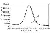
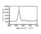
図28は、従来の原子層蒸着法により形成されたアルミニウム酸化膜のXPSグラフである。図28中、X軸は結合エネルギーを表し、Y軸は任意単位のカウントを表す。 FIG. 28 is an XPS graph of an aluminum oxide film formed by a conventional atomic layer deposition method. In FIG. 28, the X-axis represents binding energy, and the Y-axis represents arbitrary unit count.
従来のALD法により形成されたアルミニウム酸化膜のピークは535.1eVを中心として右側及び左側のグラフを重ねてみたとき、グラフが重ならずに少し広く現れるのが分かる。換言すれば、従来のALD法により形成されたアルミニウム酸化膜はAl(OH)3を含んでいるため、純粋なアルミニウム酸化膜が形成されているグラフ(a)よりも広幅のグラフ(b)が現れる。It can be seen that when the graphs on the right and left sides of the aluminum oxide film formed by the conventional ALD method are centered on 535.1 eV and the graphs on the right side and the left side are overlapped, the graphs appear a little wider without overlapping. In other words, since the aluminum oxide film formed by the conventional ALD method contains Al (OH)3 , the graph (b) wider than the graph (a) in which the pure aluminum oxide film is formed is obtained. appear.
以上のことを考慮してみるとき、従来のようにトリメチルアルミニウム及び水蒸気を直ちに反応させると、前記化学式2に示された反応によって水酸化基を含んでいるAl(OH)3がたくさん作られる。このため、Al(OH)3の量を減らすためには、水蒸気と反応するトリメチルアルミニウムの絶対量を減らしなければならない。本発明では、トリメチルアルミニウムを水酸化基を含んでいないN2Oとあらかじめ反応させてトリメチルアルミニウムの絶対量を減らした後に再び水蒸気と反応させるため、水酸化基の絶対量が少ない状態で原子層単位のアルミニウム酸化膜が形成される。Considering the above, if trimethylaluminum and water vapor are reacted immediately as in the prior art, a large amount of Al (OH)3 containing a hydroxyl group is produced by the reaction shown in
図29及び図30は各々、従来の技術及び本発明の第2実施の形態によって製造されたアルミニウム酸化膜の漏れ電流特性を示すグラフである。 29 and 30 are graphs showing leakage current characteristics of an aluminum oxide film manufactured according to the conventional technique and the second embodiment of the present invention, respectively.
アルミニウム酸化膜の漏れ電流特性をキャパシタに適用して調べてみた。ここで、キャパシタの下部電極としてはポリシリコン膜を用い、上部電極としてはポリシリコン膜を用いた。図29及び図30において、第1番目の曲線(a及びc)は下部電極をグラウンドと連結し、かつ上部電極は0〜5Vまでの電圧を印加しながら誘電膜を通じて流れるセル当たり電流の量を測定したものであり、第2番目の曲線(b及びd)は最初の測定後に再び同一の条件で測定を行った結果である。図30に示されたように、本発明によって形成されたアルミニウム酸化膜を誘電膜として採用した場合が従来の図29と比較して同一電圧、例えば2Vで漏れ電流が少なく、かつ第1番目及び第2番目の曲線間の距離も短いので、漏れ電流特性が向上されることが分かる。 The leakage current characteristic of the aluminum oxide film was examined by applying it to the capacitor. Here, a polysilicon film was used as the lower electrode of the capacitor, and a polysilicon film was used as the upper electrode. 29 and 30, the first curve (a and c) connects the lower electrode to the ground, and the upper electrode applies the voltage of 0 to 5V while applying the voltage per cell flowing through the dielectric film. The second curve (b and d) is a result of measurement again under the same conditions after the first measurement. As shown in FIG. 30, when the aluminum oxide film formed according to the present invention is used as a dielectric film, the leakage current is small at the same voltage, for example, 2 V, compared with the conventional FIG. It can be seen that the leakage current characteristic is improved because the distance between the second curves is also short.
第3の実施の形態
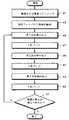
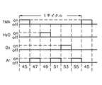
図31は、本発明の第3の実施の形態による原子層蒸着法を用いた薄膜形成方法を説明するために示すフローチャートであり、図32は、本発明の第3実施の形態による原子層蒸着法を用いた薄膜形成時に反応物の供給を示したタイミングダイアグラムである。図31及び図32では、アルミニウム酸化膜を形成する過程を例に取って説明する。Third Embodiment FIG. 31 is a flowchart for explaining a thin film forming method using an atomic layer deposition method according to a third embodiment of the present invention, and FIG. 32 is a third embodiment of the present invention. 5 is a timing diagram showing the supply of reactants when forming a thin film using an atomic layer deposition method according to the embodiment. 31 and 32, the process of forming the aluminum oxide film will be described as an example.
まず、基板15、例えばシリコン基板を酸化または窒化ガスを用いて窒素または酸素フラッシングして基板15のダングリングボンドを酸素または窒素で終端処理する(ステップ41)。前記酸素または窒素フラッシングは、図3に示された原子層薄膜形成装置をそのまま用いて行っても良く、他の装置を用いて行っても良い。そして、前記酸素または窒素フラッシングの他に、オゾン洗浄、シリコン酸化膜、シリコン窒化膜の形成などの方法を通じてもダングリングボンドを酸素または窒素と結合せしめても良い。また、必要ならば、前記基板15の酸素または窒素フラッシングは行わなくても良い。 First, a
次に、反応チャンバ11に基板15を搬入させた後に、ヒーター(図示せず)及びポンプ19を使って反応チャンバ11を100〜400℃、好ましくは、300〜350℃の温度及び1〜10,000mTorrの圧力の工程条件に保つ(ステップ43)。前記工程条件は後続するステップにおいても保たれ続くが、必要ならば変更しても良い。 Next, after the
次に、前記工程条件を保った状態で、反応チャンバ11に対して第1弁V1をオープンさせ、第1反応物11、例えばトリメチルアルミニウム(Al(CH3)3:TMA)の金属反応物をガスラインA及びシャワーヘッド17を通じて前記基板の表面を十分に覆える時間、例えば、1m秒〜10秒間注入する(ステップ45)。これにより、酸素または窒素フラッシングされた基板上に第1反応物が化学吸着される。Next, the first valve V1 is opened with respect to the
次に、前記工程条件を保った状態で、反応チャンバ11に対して選択的に第2弁V2をオープンさせ、不活性ガス、例えばアルゴンガスを0.1〜100秒間1次パージする(ステップ47)。これにより、基板15上に物理吸着された第1反応物が取り除かれる。 Next, the second valve V2 is selectively opened with respect to the
次に、前記工程条件を保った状態で、反応チャンバ11に対して第3弁V3をオープンさせ、シャワーヘッド17を通じて第2反応物、例えば水蒸気(H2O)など酸化力に優れた酸化ガスを注入する(ステップ49)。Next, the third valve V3 is opened with respect to the
これにより、前記化学吸着された第1反応物及び第2反応物は反応し、かつ化学置換によって原子層単位の薄膜、すなわちアルミニウム酸化膜が形成される。すなわち、TMAのCH3及びH2OのHは反応してCH4として取り除かれ、TMAのAl及びH2OのOは反応してAl2O3が形成される。ところが、前記原子層薄膜形成に際して、工程温度が400℃以下の低温で行われるため、TMAが完全に分解されず、その結果、アルミニウム酸化膜内に炭素やOHボンドなどの不純物がたくさん形成される。As a result, the first and second chemisorbed reactants react and a thin film in units of atomic layers, that is, an aluminum oxide film is formed by chemical substitution. That is, CH3 of TMA and H of H2 O react to be removed as CH4 , and Al of TMA and O of H2 O react to form Al2 O3 . However, since the atomic layer thin film is formed at a process temperature of 400 ° C. or lower, TMA is not completely decomposed, and as a result, many impurities such as carbon and OH bonds are formed in the aluminum oxide film. .
次に、前記工程条件を保った状態で、反応チャンバ11を不活性ガス、例えばアルゴンガスを0.1〜100秒間2次パージして前記反応されずに物理吸着されている第2反応物を取り除く(ステップ51)。 Next, in a state where the process conditions are maintained, the
次に、前記反応チャンバに前記不純物の除去及び化学量論の向上のための第3反応物、例えばオゾンなどの酸化ガスを第4弁V4及びシャワーヘッド17を通じて前記薄膜の形成された基板の表面を十分に覆る時間、例えば1m秒〜10秒間注入する(ステップ53)。このよれば、前記原子層単位の薄膜に含まれている炭素やOHボンドなどの不純物を除去できると共に、アルミニウム酸化膜の酸素欠けの問題を解決でき、その結果、優れた化学量論的な薄膜を得ることができる。 Next, a surface of the substrate on which the thin film is formed is supplied to the reaction chamber through a fourth valve V4 and a
次に、前記工程条件を保った状態で、反応チャンバ11を不活性ガスで0.1〜100秒間3次パージして反応されずに物理吸着されている第3反応物を取り除き、原子層単位の薄膜を形成する一つのサイクルを終える(ステップ55)。 Next, in a state where the above process conditions are maintained, the
次に、基板上に形成された原子層単位の薄膜の厚さの適否、例えば約10Å〜1000Åであるかどうかを確認する(ステップ57)。適宜な厚さであれば薄膜の形成段階を終え、そうでなければ前記第1反応物の注入段階(ステップ45)から不活性ガスの3次パージ段階(ステップ55)までを周期的に繰り返し行う。 Next, it is confirmed whether or not the thickness of the atomic layer unit thin film formed on the substrate is appropriate, for example, about 10 to 1000 mm (step 57). If the thickness is appropriate, the thin film formation step is completed. Otherwise, the first reactant injection step (step 45) to the inert gas tertiary purge step (step 55) are periodically repeated. .
本実施の形態において、前記第1反応物、第2反応物及び第3反応物を各々金属反応物であるトリメチルアルミニウム(Al(CH3)3:TMA)、酸化ガスである水蒸気、不純物の除去及び化学量論の向上のためのオゾンガスを用いて金属酸化膜であるアルミニウム酸化膜を形成したが、第1反応物、第2反応物及び第3反応物を各々金属反応物であるTiCl4、窒化ガスであるNH3及び不純物の除去及び化学量論の向上のための窒素ガスを用いると、金属窒化膜であるチタン窒化膜を形成することができる。In the present embodiment, the first reactant, the second reactant, and the third reactant are respectively removed from trimethylaluminum (Al (CH3 )3 : TMA) as a metal reactant, water vapor as an oxidizing gas, and impurities. In addition, an aluminum oxide film, which is a metal oxide film, is formed using ozone gas for improving stoichiometry, and the first reactant, the second reactant, and the third reactant are each converted into TiCl4 , which is a metal reactant, When nitrogen gas for removing NH3 as a nitriding gas and improving the stoichiometry is used, a titanium nitride film as a metal nitride film can be formed.
さらに、本発明の原子層蒸着法を用いた薄膜形成方法によれば、前記アルミニウム酸化膜、チタン窒化膜のほかに、単原子酸化物、複合酸化物、単原子窒化物または複合窒化物を形成することもできる。前記単原子酸化物の例としては、TiO2、Ta2O5、ZrO2、HfO2、Nb2O5、CeO2、Y2O3、SiO2、In2O3、RuO2またはIrO2等を挙げることができ、複合酸化物の例としてはSrTiO3、PbTiO3、SrRuO3、CaRuO3、(Ba,Sr)TiO3、Pb(Zr,Ti)O3、(Pb,La)(Zr,Ti)O3、(Sr,Ca)RuO3、SnがドーピングされたIn2O3、FeがドーピングされたIn2O3またはZrがドーピングされたIn2O3を挙げることができる。また、前記単原子窒化物の例としてSiN、NbN、ZrN、TaN、Ya3N5、AlN、GaN、WNまたはBNを挙げることができ、前記複合窒化物の例としてはWBN、WSiN、TiSiN、TaSiN、AlSiNまたはAlTiNを挙げることができる。Furthermore, according to the thin film formation method using the atomic layer deposition method of the present invention, in addition to the aluminum oxide film and the titanium nitride film, a monoatomic oxide, a complex oxide, a monoatomic nitride or a complex nitride is formed. You can also Examples of said monoatomicoxides, TiO 2, Ta 2 O 5 ,
また、前述した本発明の原子層蒸着法を用いた薄膜形成方法によって形成された薄膜を半導体素子に適用できる。その例としては、ゲート酸化膜、キャパシタの電極、エッチング防止膜、反応防止用キャッピング膜、写真工程時の反射防止膜、バリアー金属膜、選択蒸着用膜、金属ゲート電極等を挙げることができる。 Moreover, the thin film formed by the thin film formation method using the atomic layer deposition method of the present invention described above can be applied to a semiconductor element. Examples thereof include a gate oxide film, a capacitor electrode, an anti-etching film, a capping film for reaction prevention, an anti-reflection film during a photographic process, a barrier metal film, a film for selective vapor deposition, and a metal gate electrode.
図33は、本発明の第3の実施の形態の原子層薄膜形成方法によって形成されたアルミニウム酸化膜のサイクル当たり厚さを示すグラフである。 FIG. 33 is a graph showing the thickness per cycle of the aluminum oxide film formed by the atomic layer thin film forming method according to the third embodiment of the present invention.
図においてX軸はサイクル数を表す。ここで、一つのサイクルは、第1反応物の注入、物理吸着された第1反応物のパージ、第2反応物の注入、物理吸着された第2反応物のパージ、第3反応物の注入及び物理吸着された第3反応物のパージ段階を含む。また、Y軸はアルミニウム酸化膜の厚さを表す。図33に示されたように、本発明の薄膜製造方法によれば、アルミニウム酸化膜がサイクル当たり1.1Åの厚さで成長され、サイクル数に比例して厚さが線形的に増大するため、原子層蒸着法によりアルミニウム酸化膜が容易に形成されることが分かる。 In the figure, the X axis represents the number of cycles. Here, one cycle includes injection of the first reactant, purge of the first reactant physically adsorbed, injection of the second reactant, purge of the second reactant physically adsorbed, and injection of the third reactant. And a purge step of the physisorbed third reactant. The Y axis represents the thickness of the aluminum oxide film. As shown in FIG. 33, according to the thin film manufacturing method of the present invention, the aluminum oxide film is grown at a thickness of 1.1 mm per cycle, and the thickness increases linearly in proportion to the number of cycles. It can be seen that an aluminum oxide film can be easily formed by atomic layer deposition.
図34は、本発明の第3の実施の形態に従い原子層薄膜形成方法によって形成されたアルミニウム酸化膜の基板内の均一度を説明するために示すグラフである。 FIG. 34 is a graph shown for explaining the uniformity in the substrate of the aluminum oxide film formed by the atomic layer thin film forming method according to the third embodiment of the present invention.
X軸は8インチ基板の中央点、前記中央点を中心として1.75インチの半径を有する円から90度おきに4点、前記中央点を中心として3.5インチの半径を有する円から90度おきに4点を合わせて計9点の測定位置を表す。またY軸はアルミニウム酸化膜の厚さを表す。図34に示されたように、8インチの基板内での均一度が極めて優れていることが分かる。 The X axis is the center point of the 8-inch substrate, four points every 90 degrees from the circle having a radius of 1.75 inches centered on the center point, and 90 points from the circle having a radius of 3.5 inches centered on the center point. A total of 9 measurement positions are represented by adding 4 points every degree. The Y axis represents the thickness of the aluminum oxide film. As shown in FIG. 34, it can be seen that the uniformity within the 8-inch substrate is extremely excellent.
図35及び図36は各々、XPSを用い、従来の技術及び本発明の第3の実施の形態による原子層薄膜形成方法によって形成されたアルミニウム酸化膜のアルミニウムピークを分析したグラフである。 FIGS. 35 and 36 are graphs obtained by analyzing the aluminum peak of the aluminum oxide film formed by the conventional technique and the atomic layer thin film forming method according to the third embodiment of the present invention using XPS.
図においてX軸はボンディングエネルギーを表し、Y軸は電子の個数を表す。従来のアルミニウム酸化膜は、図35に示されたように、Al−Alボンディングがたくさん見られる。これに対し、本発明のアルミニウム酸化膜は、図36に示されたように、Al−Alボンディングはほとんど見られず、Al−Oボンディングが主として見られる。これより、本発明のアルミニウム酸化膜は化学量論に優れていることが分かる。 In the figure, the X axis represents bonding energy, and the Y axis represents the number of electrons. In the conventional aluminum oxide film, as shown in FIG. 35, many Al—Al bondings are observed. In contrast, as shown in FIG. 36, in the aluminum oxide film of the present invention, Al—Al bonding is hardly seen, and Al—O bonding is mainly seen. This shows that the aluminum oxide film of the present invention is excellent in stoichiometry.
図37及び図38は各々、XPSを用い、従来の技術及び本発明の第3の実施の形態による原子層蒸着法を用いた薄膜形成方法によって形成されたアルミニウム酸化膜の炭素ピークを分析したグラフである。 37 and 38 are graphs obtained by analyzing the carbon peak of the aluminum oxide film formed by the conventional technique and the thin film formation method using the atomic layer deposition method according to the third embodiment of the present invention using XPS, respectively. It is.
図においてX軸はボンディングエネルギーを表し、Y軸は電子の個数を表わす。従来のアルミニウム酸化膜は、図37に示されたように、炭素ピークが見られる。このことは、アルミニウム酸化膜内に炭素がたくさん含まれていることを意味する。これに対し、本発明によるアルミニウム酸化膜は、図38に示されたように、従来に比べて炭素ピークがほとんど見られない。したがって、本発明によれば、炭素などの不純物が低減されたアルミニウム酸化膜を得ることができる。 In the figure, the X axis represents bonding energy, and the Y axis represents the number of electrons. As shown in FIG. 37, the conventional aluminum oxide film has a carbon peak. This means that the aluminum oxide film contains a lot of carbon. On the other hand, in the aluminum oxide film according to the present invention, as shown in FIG. Therefore, according to the present invention, an aluminum oxide film with reduced impurities such as carbon can be obtained.
第4の実施の形態
図39は、本発明の第4の実施の形態による原子層薄膜形成方法を説明するために示すフローチャートである。図39中、図23と同一の参照番号は同一の要素を表す。Fourth Embodiment FIG. 39 is a flow chart for explaining an atomic layer thin film forming method according to a fourth embodiment of the present invention. 39, the same reference numerals as those in FIG. 23 represent the same elements.
本発明の第4の実施の形態は、第2の実施の形態及び第3の実施の形態を組み合わせた方法である。すなわち、第2の実施の形態の3次パージ後に、第3の実施の形態のように、前記反応チャンバに前記不純物の除去及び化学量論の向上のための第4反応物、例えばオゾンガスなどの酸化ガスを第3弁V3及びシャワーヘッド17を通じて前記薄膜の形成された基板の表面を十分に覆る時間、例えば1m秒〜10秒間注入した後(ステップ36a)に4次パージする(ステップ36b)ことを除いては同様である。 The fourth embodiment of the present invention is a method combining the second embodiment and the third embodiment. That is, after the third purge of the second embodiment, as in the third embodiment, the reaction chamber contains a fourth reactant such as ozone gas for removing the impurities and improving the stoichiometry. Oxidizing gas is injected through the third valve V3 and the
これにより、前記原子層単位の金属酸化膜に含まれている炭素やOHボンドなどの不純物を取り除くことができ、酸素欠けの問題を解決できるので、優れた化学量論的な薄膜を得ることができる。換言すれば、本発明は、原子層蒸着法によって薄膜を形成するに際して、主反応物のほかに、薄膜の不純物の除去及びより完全な反応を通じた薄膜の質を向上させるために、主反応物の流し込み前または流し込み後に主反応物間の反応確率を高めて所望の薄膜の質及び副産物の濃度を最小化させる。そして、本発明は、反応メカニズムにおいて水酸化基を発生させない反応物を使って薄膜内の副産物の濃度を低める。 As a result, impurities such as carbon and OH bonds contained in the metal oxide film of the atomic layer unit can be removed and the problem of oxygen deficiency can be solved, so that an excellent stoichiometric thin film can be obtained. it can. In other words, in the present invention, when forming a thin film by atomic layer deposition, in addition to the main reactant, in order to improve the quality of the thin film through removal of impurities in the thin film and more complete reaction, To increase the probability of reaction between the main reactants before or after the injection, thereby minimizing the desired film quality and byproduct concentration. The present invention lowers the concentration of by-products in the thin film using a reactant that does not generate hydroxyl groups in the reaction mechanism.
11 反応チャンバ、
11 反応物、
13 サセプタ、
15 基板、
17 シャワーヘッド、
19 ポンプ、
201 基板、
203 層間絶縁膜、
205 下部電極、
207 誘電膜、
209 上部電極、
211 キャッピング膜、
301 シリコン基板、
303 不純物ドーピング領域、
305 ゲート絶縁膜、
307 ゲート電極、
V1、V2、V3、V4 弁。11 reaction chamber,
11 reactant,
13 Susceptor,
15 substrate,
17 Shower head,
19 Pump,
201 substrate,
203 interlayer insulation film,
205 bottom electrode,
207 dielectric film,
209 upper electrode,
211 capping membrane,
301 silicon substrate,
303 impurity doping region,
305 gate insulating film,
307 gate electrode,
V1, V2, V3, V4 valves.
Claims (19)
Translated fromJapanese前記反応チャンバを不活性ガスでパージして物理吸着された第1反応物を除去する段階と、
前記反応チャンバに水酸化基を含まない第2反応物を注入して前記第1反応物と前記第2反応物との化学反応によって、第2反応物の構成要素である酸素と前記金属元素が結合し、前記第1反応物からリガンドを分離することにより前記化学吸着された第1反応物を金属−酸素原子層とする段階と、
前記反応チャンバを不活性ガスでパージして、物理吸着された第2反応物を除去する段階と、
前記反応チャンバに第3反応物を注入して前記化学吸着された第1反応物の残余分と前記第3反応物との化学反応によって、第3反応物の構成要素である酸素と前記金属元素が結合し、前記第1反応物からリガンドを分離することにより前記化学吸着された第1反応物の残余分を金属−酸素原子層として、水酸化基の生成が抑止された状態で原子層単位の金属酸化膜を形成する段階と、を含み、
前記第1反応物は金属反応物であり、前記水酸化基を含まない第2反応物はN2O、O2、O3またはCO2であり、前記第3反応物は酸化ガスであることを特徴とする原子層蒸着法を用いた薄膜形成方法。Injecting a first reactant containing a metal element and a ligand into a reaction chamber containing a substrate to chemisorb the first reactant on the substrate;
Purging the reaction chamber with an inert gas to remove the physically adsorbed first reactant;
By injecting a second reactant that does not contain a hydroxyl group into the reaction chamber and performing a chemical reaction between the first reactant and the second reactant, oxygen and the metal element constituting the second reactant are formed. Combining the chemisorbed first reactant with a metal-oxygen atomic layer by binding and separating a ligand from the first reactant;
Purging the reaction chamber with an inert gas to remove the physically adsorbed second reactant;
By injecting a third reactant into the reaction chamber and performing a chemical reaction between the remainder of the chemisorbed first reactant and the third reactant, oxygen and the metal element that are components of the third reactant And the separation of the ligand from the first reactant causes the remainder of the chemisorbed first reactant to be a metal-oxygen atomic layer, with the formation of hydroxyl groups being suppressed in an atomic layer unit.seen forming a metal oxidefilm, thefree,
The first reactant is a metal reactant, the second reactant not containing a hydroxyl group is N2O, O2, O3or CO2, and the third reactant is an oxidizing gas. A thin film forming method using an atomic layer deposition method characterized by the above.
前記反応チャンバを不活性ガスでパージして物理吸着された第1反応物を除去する段階と、
前記反応チャンバに第2反応物を注入して第1反応物と前記第2反応物との化学反応によって、前記第2反応物と前記金属元素が結合し、前記第1反応物からリガンドを分離することにより原子層単位の薄膜を形成する段階と、
前記反応チャンバを不活性ガスでパージして物理吸着された第2反応物を除去する段階と、
前記薄膜の形成された反応チャンバに不純物の除去及び化学量論の向上のために前記第2反応物と異なる第3反応物を注入する段階と、を含み、
前記第1反応物は金属反応物であり、第2及び第3反応物は酸化ガスであることを特徴とする原子層蒸着法を用いた薄膜形成方法。Injecting a first reactant containing a metal element and a ligand into a reaction chamber into which a substrate is loaded to chemisorb the first reactant on the substrate;
Purging the reaction chamber with an inert gas to remove the physically adsorbed first reactant;
A second reactant is injected into the reaction chamber, and a chemical reaction between the first reactant and the second reactant binds the second reactant and the metal element, thereby separating a ligand from the first reactant. A step of forming a thin film of atomic layer unit,
Purging the reaction chamber with an inert gas to remove the physically adsorbed second reactant;
Injecting a third reactant different from the second reactant to remove impurities and improve stoichiometry in the reaction chamber in which the thin film is formed,
Wherein the first reactant is a metal reactant, a thin film forming method using theatomic layer deposition method, wherein thesecond and third reactant is anoxidation gas.
19. The method of forming a thin film using an atomic layer deposition method according to claim18 ,wherein the steps from the first reactant injection step to thephysically adsorbed third reactantremoval stepare repeated a plurality of times .
Applications Claiming Priority (8)
| Application Number | Priority Date | Filing Date | Title |
|---|---|---|---|
| KR99P43056 | 1999-10-06 | ||
| KR19990043056 | 1999-10-06 | ||
| KR19990050902 | 1999-11-16 | ||
| KR99P50902 | 1999-11-16 | ||
| KR00P14824 | 2000-03-23 | ||
| KR20000014824 | 2000-03-23 | ||
| KR1020000053415AKR100343144B1 (en) | 1999-10-06 | 2000-09-08 | Thin film formation method using atomic layer deposition |
| KR00P53415 | 2000-09-08 |
Related Parent Applications (1)
| Application Number | Title | Priority Date | Filing Date |
|---|---|---|---|
| JP2000307849ADivisionJP4700181B2 (en) | 1999-10-06 | 2000-10-06 | Thin film formation method using atomic layer deposition |
Publications (2)
| Publication Number | Publication Date |
|---|---|
| JP2008174842A JP2008174842A (en) | 2008-07-31 |
| JP4823260B2true JP4823260B2 (en) | 2011-11-24 |
Family
ID=27350068
Family Applications (1)
| Application Number | Title | Priority Date | Filing Date |
|---|---|---|---|
| JP2008068427AExpired - Fee RelatedJP4823260B2 (en) | 1999-10-06 | 2008-03-17 | Thin film formation method using atomic layer deposition |
Country Status (2)
| Country | Link |
|---|---|
| JP (1) | JP4823260B2 (en) |
| KR (1) | KR100343144B1 (en) |
Families Citing this family (27)
| Publication number | Priority date | Publication date | Assignee | Title |
|---|---|---|---|---|
| KR100671612B1 (en)* | 2000-06-30 | 2007-01-18 | 주식회사 하이닉스반도체 | Metal deposition equipment and metal layer formation method using the same |
| KR100385947B1 (en)* | 2000-12-06 | 2003-06-02 | 삼성전자주식회사 | Method of forming thin film by atomic layer deposition |
| KR100874399B1 (en)* | 2002-07-18 | 2008-12-17 | 삼성전자주식회사 | Material formation method using atomic layer deposition method, and capacitor formation method of semiconductor device using same |
| KR20030018134A (en)* | 2001-08-27 | 2003-03-06 | 한국전자통신연구원 | Method of forming an insulation layer of a semiconductor device for controlling the composition and the doping concentration |
| KR100418569B1 (en)* | 2001-12-10 | 2004-02-14 | 주식회사 하이닉스반도체 | Method for forming high dielectric thin film using atomic layer deposition |
| KR100473113B1 (en)* | 2002-04-04 | 2005-03-08 | 삼성전자주식회사 | Method Of Fabricating A Capacitor Of Semiconductor Device |
| KR20030089066A (en)* | 2002-05-16 | 2003-11-21 | 주성엔지니어링(주) | Method of fabricating Ru film for use in semiconductor devices |
| JP3920235B2 (en)* | 2003-03-24 | 2007-05-30 | 株式会社ルネサステクノロジ | Manufacturing method of semiconductor device |
| KR100994072B1 (en)* | 2003-06-16 | 2010-11-12 | 주성엔지니어링(주) | Atomic Layer Deposition of Aluminum Oxide Films |
| KR100594626B1 (en)* | 2004-09-02 | 2006-07-07 | 한양대학교 산학협력단 | Nitride Film Formation Method Using Atomic Layer Deposition |
| KR100695889B1 (en) | 2004-10-11 | 2007-03-19 | 삼성전자주식회사 | Capacitor having a reaction prevention film and a method of forming the same |
| KR100773755B1 (en)* | 2004-11-18 | 2007-11-09 | 주식회사 아이피에스 | Plasma ALD Thin Film Deposition Method |
| KR20060072338A (en) | 2004-12-23 | 2006-06-28 | 주식회사 하이닉스반도체 | Dielectric film formation method and capacitor formation method of semiconductor device using same |
| KR100744026B1 (en)* | 2005-06-28 | 2007-07-30 | 주식회사 하이닉스반도체 | Manufacturing Method of Flash Memory Device |
| KR101101785B1 (en)* | 2007-06-08 | 2012-01-05 | 도쿄엘렉트론가부시키가이샤 | Patterning method |
| JP2009088229A (en)* | 2007-09-28 | 2009-04-23 | Tokyo Electron Ltd | Film forming apparatus, film forming method, storage medium, and gas supply apparatus |
| JP5672685B2 (en)* | 2009-09-29 | 2015-02-18 | 富士電機株式会社 | Manufacturing method of semiconductor device |
| US8637123B2 (en)* | 2009-12-29 | 2014-01-28 | Lotus Applied Technology, Llc | Oxygen radical generation for radical-enhanced thin film deposition |
| JP5696530B2 (en)* | 2010-05-01 | 2015-04-08 | 東京エレクトロン株式会社 | Thin film forming method and film forming apparatus |
| KR101213291B1 (en)* | 2010-12-30 | 2012-12-18 | 부산대학교 산학협력단 | Method And System for forming a thin film using an Liquid-Vapor Hybrid Atomic Layer Deposition Method |
| JP2015149461A (en)* | 2014-02-10 | 2015-08-20 | 東京エレクトロン株式会社 | Method and apparatus for forming metal oxide film |
| KR101727259B1 (en) | 2015-03-18 | 2017-04-17 | 연세대학교 산학협력단 | Method and apparatus for forming oxide thin film |
| KR102095710B1 (en)* | 2019-11-05 | 2020-04-01 | 주식회사 유진테크 머티리얼즈 | Method of depositing thin films using protective material |
| CN113140452A (en)* | 2021-04-21 | 2021-07-20 | 北海惠科光电技术有限公司 | Indium tin oxide nanowire, preparation method thereof and thin film transistor |
| JP7039085B1 (en)* | 2021-08-30 | 2022-03-22 | 株式会社クリエイティブコーティングス | Film forming equipment |
| KR102690226B1 (en)* | 2022-06-16 | 2024-08-05 | 한국생산기술연구원 | Thin film transistor and manufacturing method thereof |
| CN118380510B (en)* | 2024-06-21 | 2024-10-29 | 无锡松煜科技有限公司 | Method for preparing laminated alumina film layer based on ALD (atomic layer deposition) process |
Family Cites Families (10)
| Publication number | Priority date | Publication date | Assignee | Title |
|---|---|---|---|---|
| JP2789587B2 (en)* | 1988-01-08 | 1998-08-20 | 日本電気株式会社 | Manufacturing method of insulating thin film |
| JP2663471B2 (en)* | 1988-01-08 | 1997-10-15 | 日本電気株式会社 | Manufacturing method of insulating thin film |
| JP2648211B2 (en)* | 1989-08-10 | 1997-08-27 | 日本電信電話株式会社 | Preparation method of oxide thin film |
| JPH05323373A (en)* | 1992-05-22 | 1993-12-07 | Fujitsu Ltd | Production of thin film transistor panel |
| JPH0786269A (en)* | 1993-09-10 | 1995-03-31 | Fujitsu Ltd | Alumina film forming method and thin film transistor manufacturing method using the same |
| JPH07252660A (en)* | 1994-01-19 | 1995-10-03 | Rikagaku Kenkyusho | Thin film manufacturing method and manufacturing apparatus thereof |
| US5916365A (en)* | 1996-08-16 | 1999-06-29 | Sherman; Arthur | Sequential chemical vapor deposition |
| KR100252049B1 (en)* | 1997-11-18 | 2000-04-15 | 윤종용 | The atomic layer deposition method for fabricating aluminum layer |
| KR19990074809A (en)* | 1998-03-14 | 1999-10-05 | 윤종용 | Thin Film Manufacturing Method |
| KR100275738B1 (en)* | 1998-08-07 | 2000-12-15 | 윤종용 | Method for producing thin film using atomatic layer deposition |
- 2000
- 2000-09-08KRKR1020000053415Apatent/KR100343144B1/ennot_activeExpired - Fee Related
- 2008
- 2008-03-17JPJP2008068427Apatent/JP4823260B2/ennot_activeExpired - Fee Related
Also Published As
| Publication number | Publication date |
|---|---|
| KR100343144B1 (en) | 2002-07-05 |
| JP2008174842A (en) | 2008-07-31 |
| KR20010039874A (en) | 2001-05-15 |
Similar Documents
| Publication | Publication Date | Title |
|---|---|---|
| JP4823260B2 (en) | Thin film formation method using atomic layer deposition | |
| JP4700181B2 (en) | Thin film formation method using atomic layer deposition | |
| US6576053B1 (en) | Method of forming thin film using atomic layer deposition method | |
| US7396719B2 (en) | Method of forming high dielectric film using atomic layer deposition and method of manufacturing capacitor having the high dielectric film | |
| US6806145B2 (en) | Low temperature method of forming a gate stack with a high k layer deposited over an interfacial oxide layer | |
| KR101712040B1 (en) | Processes for passivating dielectric films | |
| US7087482B2 (en) | Method of forming material using atomic layer deposition and method of forming capacitor of semiconductor device using the same | |
| KR100546324B1 (en) | Metal oxide thin film formation method by ALD, lanthanum oxide film formation method and high-k dielectric film formation method of semiconductor device | |
| KR100591507B1 (en) | Atomic layer deposition of nanolaminate film | |
| US20070098892A1 (en) | Method of forming a layer and method of manufacturing a capacitor using the same | |
| JP2004056142A (en) | Material forming method using atomic layer deposition and method for forming capacitor of semiconductor device using the same | |
| US8735305B2 (en) | Methods of forming fluorinated hafnium oxide gate dielectrics by atomic layer deposition | |
| JP3941099B2 (en) | Thin film formation method | |
| KR100560963B1 (en) | Method of forming material using atomic layer deposition process, method of forming thin film, and method of forming capacitor using the same | |
| US20060240679A1 (en) | Method of manufacturing semiconductor device having reaction barrier layer | |
| KR102831287B1 (en) | Carbon-free laminated hafnium oxide/zirconium oxide films for ferroelectric memory | |
| JP2007081410A (en) | Ferroelectric film, ferroelectric capacitor forming method, and ferroelectric capacitor | |
| KR20070106286A (en) | Method for forming titanium oxide film crystallized in rutile structure and method for manufacturing capacitor using same | |
| KR100920402B1 (en) | Low temperature gate stack | |
| KR100780605B1 (en) | Semiconductor device with tantalum zirconium oxide film and manufacturing method thereof | |
| KR20070098286A (en) | Method of manufacturing capacitors in semiconductor devices | |
| EP1425785A2 (en) | Method of fabricating a gate stack at low temperature |
Legal Events
| Date | Code | Title | Description |
|---|---|---|---|
| A131 | Notification of reasons for refusal | Free format text:JAPANESE INTERMEDIATE CODE: A131 Effective date:20110419 | |
| A521 | Written amendment | Free format text:JAPANESE INTERMEDIATE CODE: A523 Effective date:20110715 | |
| TRDD | Decision of grant or rejection written | ||
| A01 | Written decision to grant a patent or to grant a registration (utility model) | Free format text:JAPANESE INTERMEDIATE CODE: A01 Effective date:20110809 | |
| A01 | Written decision to grant a patent or to grant a registration (utility model) | Free format text:JAPANESE INTERMEDIATE CODE: A01 | |
| A61 | First payment of annual fees (during grant procedure) | Free format text:JAPANESE INTERMEDIATE CODE: A61 Effective date:20110906 | |
| R150 | Certificate of patent or registration of utility model | Ref document number:4823260 Country of ref document:JP Free format text:JAPANESE INTERMEDIATE CODE: R150 Free format text:JAPANESE INTERMEDIATE CODE: R150 | |
| FPAY | Renewal fee payment (event date is renewal date of database) | Free format text:PAYMENT UNTIL: 20140916 Year of fee payment:3 | |
| R250 | Receipt of annual fees | Free format text:JAPANESE INTERMEDIATE CODE: R250 | |
| R250 | Receipt of annual fees | Free format text:JAPANESE INTERMEDIATE CODE: R250 | |
| R250 | Receipt of annual fees | Free format text:JAPANESE INTERMEDIATE CODE: R250 | |
| R250 | Receipt of annual fees | Free format text:JAPANESE INTERMEDIATE CODE: R250 | |
| R250 | Receipt of annual fees | Free format text:JAPANESE INTERMEDIATE CODE: R250 | |
| R250 | Receipt of annual fees | Free format text:JAPANESE INTERMEDIATE CODE: R250 | |
| LAPS | Cancellation because of no payment of annual fees |