JP4818928B2 - Method and apparatus for receiver detection on a PCI Express bus - Google Patents
Method and apparatus for receiver detection on a PCI Express busDownload PDFInfo
- Publication number
- JP4818928B2 JP4818928B2JP2006541127AJP2006541127AJP4818928B2JP 4818928 B2JP4818928 B2JP 4818928B2JP 2006541127 AJP2006541127 AJP 2006541127AJP 2006541127 AJP2006541127 AJP 2006541127AJP 4818928 B2JP4818928 B2JP 4818928B2
- Authority
- JP
- Japan
- Prior art keywords
- receiver
- voltage
- common
- mode voltage
- detector
- Prior art date
- Legal status (The legal status is an assumption and is not a legal conclusion. Google has not performed a legal analysis and makes no representation as to the accuracy of the status listed.)
- Expired - Fee Related
Links
- 238000000034methodMethods0.000titleclaimsdescription11
- 238000001514detection methodMethods0.000titledescription14
- 238000002347injectionMethods0.000claims2
- 239000007924injectionSubstances0.000claims2
- 230000000977initiatory effectEffects0.000claims1
- 239000000872bufferSubstances0.000description15
- 238000010586diagramMethods0.000description14
- 230000005540biological transmissionEffects0.000description12
- 230000008878couplingEffects0.000description10
- 238000010168coupling processMethods0.000description10
- 238000005859coupling reactionMethods0.000description10
- 239000003990capacitorSubstances0.000description9
- 230000002093peripheral effectEffects0.000description5
- 230000000630rising effectEffects0.000description4
- 230000008901benefitEffects0.000description2
- 230000003071parasitic effectEffects0.000description2
- 238000012545processingMethods0.000description2
- 238000004891communicationMethods0.000description1
- 238000012546transferMethods0.000description1
Images


Classifications
- H—ELECTRICITY
- H04—ELECTRIC COMMUNICATION TECHNIQUE
- H04L—TRANSMISSION OF DIGITAL INFORMATION, e.g. TELEGRAPHIC COMMUNICATION
- H04L25/00—Baseband systems
- H04L25/02—Details ; arrangements for supplying electrical power along data transmission lines
- H04L25/0264—Arrangements for coupling to transmission lines
- H04L25/0272—Arrangements for coupling to multiple lines, e.g. for differential transmission
- H04L25/0274—Arrangements for ensuring balanced coupling
- H—ELECTRICITY
- H04—ELECTRIC COMMUNICATION TECHNIQUE
- H04L—TRANSMISSION OF DIGITAL INFORMATION, e.g. TELEGRAPHIC COMMUNICATION
- H04L1/00—Arrangements for detecting or preventing errors in the information received
- H04L1/22—Arrangements for detecting or preventing errors in the information received using redundant apparatus to increase reliability
- H—ELECTRICITY
- H04—ELECTRIC COMMUNICATION TECHNIQUE
- H04L—TRANSMISSION OF DIGITAL INFORMATION, e.g. TELEGRAPHIC COMMUNICATION
- H04L25/00—Baseband systems
- H04L25/38—Synchronous or start-stop systems, e.g. for Baudot code
- H04L25/40—Transmitting circuits; Receiving circuits
- H04L25/45—Transmitting circuits; Receiving circuits using electronic distributors
Landscapes
- Engineering & Computer Science (AREA)
- Computer Networks & Wireless Communication (AREA)
- Signal Processing (AREA)
- Power Engineering (AREA)
- Logic Circuits (AREA)
Description
Translated fromJapanese関連出願の相互参照
本出願は、2003年11月18日に出願した米国仮出願第60/520,917号の利点を主張するものである。
本発明は一般に、受信機検出技法に関し、具体的には、周辺構成要素相互接続イクスプレス(Peripheral Component Interconnect Express)リンク・システム上で受信機を検出する方法および装置に係る。This application claims the benefit of US Provisional Application No. 60 / 520,917, filed Nov. 18, 2003.
The present invention relates generally to receiver detection techniques, and more particularly to a method and apparatus for detecting a receiver on a Peripheral Component Interconnect Express Express link system.
Peripheral Component Interconnect(PCI)仕様(WWW.pci-sig.comからダウンロード可能)は、1つまたは複数の周辺装置が、シリアル入出力バスリンクを介してコンピュータ装置と通信できる方法を定義する。シリアル・リンクは、単一のコンピュータ装置内にあっても、1つまたは複数のコンピュータ装置および周辺装置をリンクしてもよい。当初のPCI仕様は、毎秒132メガバイトのピーク・スループットで33MHzで動作する32ビットPCIバスを定義する。最近まで、当初のPCI仕様のパフォーマンスは、ほとんどのアプリケーションに十分なものであった。市販のプロセッサの処理速度が増大してきたため、データを処理するプロセッサの処理能力は結果的に、PCIバスのデータ搬送能力を超えてしまった。したがって、近年のプロセッサは、PCIバスがデータをプロセッサに搬送できる速度よりも速くデータを処理することができる。
PCI Expressと呼ばれるPCI仕様の最新バージョンは、プロセッサと、ネットワーク・カード、プリンタ、およびストレージ・ディスクなどのさまざまな周辺装置との間のデータのフローを増大させることにより、コンピュータのパフォーマンスを向上させることを提案する。最大伝送速度を制限するパラレル・バス上でデータを伝送するのではなく、毎秒2.5ギガビット以上の高速シリアル・レーンを使用してデータを伝送する。複数レーン、たとえば32レーンが使用される場合、最大速度は毎秒80ギガビットまで高めることができる。 The latest version of the PCI specification, called PCI Express, improves computer performance by increasing the flow of data between the processor and various peripheral devices such as network cards, printers, and storage disks. Propose. Rather than transmitting data on a parallel bus that limits the maximum transmission rate, data is transmitted using a high-speed serial lane of 2.5 gigabits per second or higher. If multiple lanes are used, for example 32 lanes, the maximum speed can be increased to 80 gigabits per second.
さらに、PCI Expressは、バスの信頼性、タイミングおよびスケーラビリティを改善すると考えられるいくつかの新機能を含んでいる。たとえば、PCI Express規格は、通信リンクのはるか向こう側に受信機があるかどうかを送信機が判別できるようにする「受信機検出」機能をサポートする。したがって、PCI Expressバス経由で通信する送信機で採用することができる受信機検出器が必要とされている。 In addition, PCI Express includes several new features that are believed to improve bus reliability, timing, and scalability. For example, the PCI Express standard supports a “receiver detection” feature that allows a transmitter to determine if a receiver is far beyond the communication link. Therefore, there is a need for a receiver detector that can be employed in transmitters that communicate via a PCI Express bus.
一般に、PCI Expressバス上の受信機を検出するための方法および装置が提供される。受信機は、1つまたは複数の送信機出力ノードに注入された電流を使用して同相電圧を調整し、電圧変化率に基づいて受信機が存在するかどうかを検出することにより、PCI Expressリンク上で検出される。たとえば、電流は、振幅制御回路の制御下で電荷ポンプによって注入することができる。さまざまな実施形態において、電荷ポンプは、CML送信バッファまたはHブリッジ型の送信バッファと統合することができる。 In general, a method and apparatus are provided for detecting a receiver on a PCI Express bus. The receiver adjusts the common-mode voltage using current injected into one or more transmitter output nodes and detects whether the receiver is present based on the voltage change rate, thereby providing a PCI Express link. Detected above. For example, the current can be injected by a charge pump under the control of an amplitude control circuit. In various embodiments, the charge pump can be integrated with a CML transmission buffer or an H-bridge type transmission buffer.
振幅制御回路はオプションで、調整された同相電圧を1つまたは複数のあらかじめ定められた電圧と比較して、調整された同相電圧を2つのあらかじめ定められた電圧の間で保持することができる。振幅制御回路は、送信機出力ノードに注入された電流を制御するために電荷ポンプに信号を提供する。振幅制御回路もまた、模範的なタイマーに信号を提供する。タイマーは、同相電圧の変化率を測定して受信機が存在するかどうかを判別し、オプションで受信機が存在するかどうかを示す検出出力フラグを生成する。
本発明と、本発明のさらに多くの特徴および利点は、以下の詳細な説明および図を参照することによってさらに深く理解されるであろう。The amplitude control circuit can optionally compare the adjusted common-mode voltage with one or more predetermined voltages and hold the adjusted common-mode voltage between the two predetermined voltages. The amplitude control circuit provides a signal to the charge pump to control the current injected into the transmitter output node. The amplitude control circuit also provides a signal to an exemplary timer. The timer measures the rate of change of the common mode voltage to determine whether a receiver is present and optionally generates a detection output flag indicating whether the receiver is present.
The invention and many more features and advantages of the invention will be better understood with reference to the following detailed description and drawings.
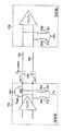
本発明は、以下で図2を参照して説明する、PCI Expressリンク150経由で通信する送信機110に使用するための受信機検出器250を提供する。図1Aは、差動伝送回線150を介して通信する送信機110および受信機170の概略ブロック図である。送信機110および受信機170のAC結合は、結合コンデンサ160を通じて使用される。図1Aに示すように、送信機110は、差動伝送回線150と接地の間の抵抗器115、120のペアを含んでいる。同様に、送信機170は、差動伝送回線150と接地の間の抵抗器175、180のペアを含んでいる。抵抗器115、120、175、180は、より高速な反射を回避するために差動伝送回線150を終端する。抵抗器115、120、175、180は通常、50オーム程度の抵抗値を有している。 The present invention provides a receiver detector 250 for use with a
本発明は、受信機170が存在し、伝送回線150に接続されている場合、受信終端抵抗器175、180を介して接地に接続されている大型AC結合コンデンサ160が送信機への負荷として動作することを認識する。電圧段階的変化がノードVxに適用される場合、out+およびoutーにおける電圧はVxの変化に従う。しかし、送信機110の出力、out+およびout−における電圧変化率は、X*Cac,couplingとほぼ等しい時定数によって決まる。ここで、Xは送信機110の出力インピーダンス(つまり、終端抵抗器115、120の単位オームの値)であり、Cac,couplingはAC結合コンデンサ160の単位ファラドの値である。In the present invention, when the
図1Bに示すように、受信機が存在しない場合、受信機170の終端抵抗器175、180は存在せず、送信機110によって認められる負荷は、padキャパシタンス、CPAD165と呼ばれる、ノードout+およびout−に関連付けられている寄生コンデンサのみになる。送信機110の出力、out+およびoutoーにおける電圧変化率は、時定数X*CPADによって決まる。As shown in FIG. 1B, if no receiver is present, the
AC結合コンデンサ160のキャパシタンスが、padコンデンサ165のキャパシタンスよりもはるかに大きいので、受信機170が存在するかどうかに応じて、大幅で測定可能な電圧変化率の差異が観察される。本発明の1つの態様によれば、電圧変化率と呼ばれる、送信機110の出力の期間は、受信機170がPCI Expressリンク150上に存在するかどうかを判別するために使用される。リンク150は大型結合コンデンサ160にAC結合され、受信機170(存在する場合)は50オームの抵抗器175、180で終端されているので、本発明による受信機検出器は、送信機110の電圧変化率を測定することにより受信機170が存在するかどうかを検出する。 Since the capacitance of the
図2は、本発明の特徴を組み込む送信機200を示す概略ブロック図である。図2に示すように、送信機200は受信機検出器250を含んでいる。一般に、受信機検出器250は、送信機200における電圧変化率を測定することにより、受信機(図示せず)が存在するかどうかを検出する。1つの模範的な実施形態において、受信機検出器250は、送信機200の出力共通電圧Vxを変化させ、送信機出力ノードout+およびout−における電圧変化率を検出する。前述のように、受信機が存在する場合、電圧変化率は、時定数X*Cac,couplingによってほぼ決まる。同様に、受信機が存在しない場合、電圧変化率は、時定数X*CPADによってほぼ決まる。受信機検出器250は、測定された電圧変化率をしきい値と比較して、受信機が存在するかどうかを判別する。FIG. 2 is a schematic block diagram illustrating a
図2に示す1つの模範的な実施形態において、受信機検出器250は、図3と併せて以下でさらに説明される振幅制御回路230に関連付けられている、図4と併せて以下でさらに説明される電荷ポンプ240を採用して、送信機200の出力同相(CM)電圧を変える。一般に、受信機検出器250は、弛張発振器として動作する。負荷ポンプ240は、送信機200の出力ノードout+およびout−に電流を注入し、これにより送信機200の同相(CM)電圧を変化させる。同相検出器205は、送信機200の出力CM電圧を測定する。図2に示すように、同相検出器205は、送信機出力ノードout+およびout−間に直列に接続されている2つの抵抗器210、220として実装される。抵抗器210、220の値は、送信機200の終端抵抗器115、120と比べて大きい。 In one exemplary embodiment shown in FIG. 2, the receiver detector 250 is further described below in conjunction with FIG. 4, associated with an
図3と併せて以下でさらに説明される振幅制御回路230は、送信機200の測定されたCM電圧Vcmを、あらかじめ定められた電圧Vref1およびVref2と比較して、電荷ポンプ240によって導入されたCM電圧変化がVref1とVref2の間であることを確認する。タイマー245は、CM電圧、Vcmの変化率を測定して、受信機が存在するかどうかを判別する。タイマー245は、受信機が存在するかどうかを示す検出出力フラグを生成する。たとえばタイマー245は、1のバイナリ値を有するフラグを生成して受信機が存在することを示すか、またはゼロのバイナリ値を有するフラグを生成して受信機が存在しないことを示すことができる。タイマー245は、クロック信号によって駆動される。The
図3は、図2の模範的な振幅制御回路230をさらに詳細に示す概略ブロック図である。図3に示すように、振幅制御回路230は、電圧比較器のペア310、320、反転出力を有するNANDゲートのペア330、340、およびインバータ350を含んでいる。作動中、受信機検出プロセスを開始すると、送信バッファ270(図2)はオフにされ、送信機200は高CM出力インピーダンス・モードになる。送信機200の測定されたCM電圧、Vcmが電圧Vref2よりも大きい(Vcm>Vref2)場合、下降制御信号DNは使用可能であり、上昇制御信号UPは使用不可である。その結果、負荷ポンプ240は、Vref1に向けてout+/out−の電圧(図2)を変える。FIG. 3 is a schematic block diagram illustrating the exemplary
送信機200の測定されたCM電圧、Vcmが電圧Vref1よりも小さい(Vcm<Vref1)場合、下降制御信号DNは使用不可であり、上昇制御信号UPは使用可能である。その結果、負荷ポンプ240は、Vref2に向けてout+/out−の電圧(図2)を変える。When the measured CM voltage Vcm of the transmitter 200 is smaller than the voltage Vref1 (Vcm <Vref1), the lowering control signal DN is not usable and the rising control signal UP is usable. As a result, the
図4は、図2の模範的な電荷ポンプ240をさらに詳細に示す概略ブロック図である。図4に示すように、負荷ポンプ240は、2つのPMOSトランジスタ410、430と、2つのNMOSトランジスタ420、440と、2つの電流源450、460を含んでいる。トランジスタ410、430、420、440は、図3の振幅制御回路230によって生成されたUPおよびDN制御信号にそれぞれ接続されている。上昇電流源450は、UP制御信号が振幅制御回路230によって使用可能になる場合(つまりVcm<Vref1)、アクティブになる。上昇電流源450がアクティブの場合、負荷ポンプ240は、Vref2に向けてout+/out−の電圧を変える。同様に、下降電流源460は、DN制御信号が振幅制御回路230によって使用可能になる場合(つまりVcm>Vref2)、アクティブになる。下降電流源460がアクティブの場合、負荷ポンプ240は、Vref1に向けてout+/out−の電圧を変える。 FIG. 4 is a schematic block diagram illustrating the
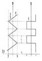
図5は、同相電圧Vcm、(Vout+/Vout−)510およびUP制御信号520を示している。図5に示すように、同相電圧Vcmは、前述のような方法でUPおよびDN制御信号の選択的な適用によりVref1およびVref2の間で保持されている。前述のように、タイマー245(図2)は、CM電圧Vcmの変化率を測定して、受信機が存在するかどうかを判別する。タイマー245は、UPまたはDN制御信号の期間tを測定することによりVcmの変化率を測定する。期間tは、Vcm変化率に反比例する。期間tが特定のしきい値を超える場合(しきい値は使用されるPADコンデンサ、CPAD165およびAC結合コンデンサ160の実効値に依存している)、タイマー245の出力は、受信機の存在を示す1のバイナリ値に設定される。期間tが特定のしきい値よりも小さい場合、タイマー245の出力は、受信機が存在しないこと示す0のバイナリ値に設定される。FIG. 5 shows the common mode voltage Vcm, (Vout + / Vout−) 510 and the
図6は、電流モード論理(CML)送信バッファ270が使用される場合に採用することのできる代替電荷ポンプを示す概略ブロック図である。回路600は、CMLバッファに組み込まれている電荷ポンプを含んでいる。CMLバッファは、高速バッファ設計に使用されることが多い。図6に示す電荷ポンプは、寄生キャパシタンスを最小化するために、CMLバッファ270内の既存トランジスタを共有することを目的としている。図4と併せて前述された電荷ポンプ240は、CMLバッファで簡略化することができる。 FIG. 6 is a schematic block diagram illustrating an alternative charge pump that may be employed when a current mode logic (CML) transmit
図6に示すように、CMLバッファ610は、受信機検出モードで開放位置、データ・モードで閉鎖位置にできる第1のスイッチS1によって制御される。さらに、集積回路600は、上昇電流源、Iup、620が回路600に含まれているかどうかを判別する第2のスイッチS2を含んでいる。第2のスイッチS2は、データ・モードで開放位置、受信機検出モードで閉鎖位置にある。As shown in FIG. 6, the
トランジスタM1およびM2のゲート制御信号は、2つのマルチプレクサ620、640によって制御される。受信機検出モードにある場合、2つのマルチプレクサ630、640は、出力信号A、Bが下降制御信号、DNと同じ値を有するように設定される。データ送信モードにある場合、2つのマルチプレクサ630、640は、出力信号A、Bがそれぞれのデータ信号、Data_PおよびData_Nと同じ値を有するように設定される。電流源Issは、受信機検出モード、IssがIupと等しくなるようにプログラム可能にすることができる。出力同相電圧、VcMは、ノードVcMにおいて直接検知される。The gate control signals for transistors M1 and M2 are controlled by two multiplexers 620,640. When in receiver detection mode, the two
図7は、Hブリッジ型の送信バッファ710が使用される場合に採用することのできる代替電荷ポンプを示す概略ブロック図である。回路700は、Hブリッジ型のバッファ710に組み込まれている電荷ポンプを含んでいる。Hブリッジバッファ710は、4つのトランジスタM1からM4を含んでおり、受信機検出モードで電荷ポンプとして設定することができる。図7に示すように、4つのマルチプレクサ720、730、740、750は、受信機検出モードにおいてUP/DN信号を(振幅制御回路230から)選択するか、または通常の送信モードにおいて入力としてDATA入力を選択するために使用される。電流源I1およびI2は、図2の電流源IUPおよびIDNと同様の方法で、UPおよびDN制御信号に従って受信機検出モードで異なる値に設定することができる。CM電圧、VCMは、図7に示すように、2つの終端抵抗器R1およびR2の中間点で直接検知することができる。受信機検出制御プロセスは、図2と併せて上記で説明したように実行することができる。FIG. 7 is a schematic block diagram showing an alternative charge pump that can be employed when an H-
本明細書に述べてきた実施例および変形は、本発明の理念を示したものに過ぎず、当業者により本発明の範囲および精神を逸脱することなくさまざまな変更を加えることができることを理解されたい。 It will be understood that the embodiments and variations described herein are merely illustrative of the spirit of the invention and that various changes may be made by those skilled in the art without departing from the scope and spirit of the invention. I want.
Claims (10)
Translated fromJapanese1つまたは複数の送信機出力ノードに電流を注入することにより同相電圧を調整するステップと、
電圧変化率に基づいて受信機が前記PCI Expressリンク上に存在するかどうかを検出するステップとを備える方法。A method for determining whether a receiver is present on a PCI Express link, comprising:
Adjusting the common-mode voltage by injecting current into one or more transmitter output nodes;
Detecting whether a receiver is present on the PCI Express link based on a voltage rate of change.
電圧変化率に基づいて受信機が前記PCI Expressリンク上に存在するかどうかを検出するためのタイマーとを備える検出器。A receiver detector for use with a transmitter connected to a PCI Express link, wherein the amplitude control circuit adjusts the common mode voltage by initiating current injection into one or more transmitter output nodes;
A detector for detecting whether a receiver is present on the PCI Express link based on a voltage change rate.
Applications Claiming Priority (5)
| Application Number | Priority Date | Filing Date | Title |
|---|---|---|---|
| US52091703P | 2003-11-18 | 2003-11-18 | |
| US60/520,917 | 2003-11-18 | ||
| US10/822,027US7222290B2 (en) | 2003-11-18 | 2004-04-09 | Method and apparatus for receiver detection on a PCI-Express bus |
| US10/822,027 | 2004-04-09 | ||
| PCT/US2004/024544WO2005057414A1 (en) | 2003-11-18 | 2004-07-29 | Method and apparatus for receiver detection on a pci-express bus |
Publications (3)
| Publication Number | Publication Date |
|---|---|
| JP2007511846A JP2007511846A (en) | 2007-05-10 |
| JP2007511846A5 JP2007511846A5 (en) | 2007-09-13 |
| JP4818928B2true JP4818928B2 (en) | 2011-11-16 |
Family
ID=34577040
Family Applications (1)
| Application Number | Title | Priority Date | Filing Date |
|---|---|---|---|
| JP2006541127AExpired - Fee RelatedJP4818928B2 (en) | 2003-11-18 | 2004-07-29 | Method and apparatus for receiver detection on a PCI Express bus |
Country Status (5)
| Country | Link |
|---|---|
| US (1) | US7222290B2 (en) |
| EP (1) | EP1687726B1 (en) |
| JP (1) | JP4818928B2 (en) |
| DE (1) | DE602004009100T2 (en) |
| WO (1) | WO2005057414A1 (en) |
Families Citing this family (27)
| Publication number | Priority date | Publication date | Assignee | Title |
|---|---|---|---|---|
| US7669190B2 (en) | 2004-05-18 | 2010-02-23 | Qlogic, Corporation | Method and system for efficiently recording processor events in host bus adapters |
| US7577772B2 (en)* | 2004-09-08 | 2009-08-18 | Qlogic, Corporation | Method and system for optimizing DMA channel selection |
| US7404090B1 (en)* | 2004-10-15 | 2008-07-22 | National Semiconductor Corporation | Device and computer system for power management using serial link connections |
| US7392437B2 (en)* | 2005-01-20 | 2008-06-24 | Qlogic, Corporation | Method and system for testing host bus adapters |
| US7231480B2 (en)* | 2005-04-06 | 2007-06-12 | Qlogic, Corporation | Method and system for receiver detection in PCI-Express devices |
| US8021193B1 (en) | 2005-04-25 | 2011-09-20 | Nvidia Corporation | Controlled impedance display adapter |
| US7793029B1 (en) | 2005-05-17 | 2010-09-07 | Nvidia Corporation | Translation device apparatus for configuring printed circuit board connectors |
| US7698484B2 (en)* | 2005-09-21 | 2010-04-13 | Ricoh Co., Ltd. | Information processor configured to detect available space in a storage in another information processor |
| US7694062B1 (en)* | 2005-11-01 | 2010-04-06 | Nvidia Corporation | System and apparatus for capacitively coupling signals with an integrated circuit |
| US7461195B1 (en) | 2006-03-17 | 2008-12-02 | Qlogic, Corporation | Method and system for dynamically adjusting data transfer rates in PCI-express devices |
| JP5108261B2 (en)* | 2006-07-11 | 2012-12-26 | 株式会社リコー | Information processing apparatus and data communication apparatus |
| US7768306B2 (en)* | 2006-09-20 | 2010-08-03 | Mediatek Inc. | Low to high voltage conversion output driver |
| DE102007003230B4 (en)* | 2007-01-22 | 2018-07-26 | Infineon Technologies Ag | Method, apparatus and circuit for determining a state of a receiver on a transmission line |
| US7471512B1 (en)* | 2007-09-28 | 2008-12-30 | Emc Corporation | Storage system assembly employing repeater amplifiers in I/O expansion module |
| JP5096905B2 (en) | 2007-12-20 | 2012-12-12 | 株式会社日立製作所 | Server apparatus and link recovery processing method thereof |
| US8415999B2 (en)* | 2010-07-28 | 2013-04-09 | International Business Machines Corporation | High frequency quadrature PLL circuit and method |
| US8174294B1 (en) | 2010-10-22 | 2012-05-08 | Altera Corporation | Configurable buffer circuits and methods |
| JP2012115545A (en)* | 2010-12-02 | 2012-06-21 | Nidek Co Ltd | Living tissue stimulation circuit |
| US9015357B2 (en)* | 2012-10-22 | 2015-04-21 | Ati Technologies Ulc | Method and device for providing high speed data transmission with video data |
| US9235543B2 (en)* | 2012-11-26 | 2016-01-12 | International Business Machines Corporation | Systems for signal detection |
| US8989313B2 (en) | 2013-03-11 | 2015-03-24 | International Business Machines Corporation | Adaptable receiver detection |
| US9906383B2 (en) | 2015-02-02 | 2018-02-27 | Samsung Electronics Co., Ltd. | Semiconductor device, semiconductor system and method of operating semiconductor device |
| US10048731B2 (en)* | 2015-06-26 | 2018-08-14 | Intel Corporation | Mitigation of charging induced voltage offset |
| JP6744605B2 (en)* | 2016-07-29 | 2020-08-19 | ザインエレクトロニクス株式会社 | Transmission device and transmission/reception system |
| JP7059860B2 (en)* | 2018-08-06 | 2022-04-26 | 富士通株式会社 | Parameter setting Transmission / reception system and parameter setting method |
| JP7578046B2 (en)* | 2021-03-31 | 2024-11-06 | 株式会社デンソー | Differential communication driver circuit |
| TWI813144B (en)* | 2022-01-25 | 2023-08-21 | 瑞昱半導體股份有限公司 | Receiver detection system and receiver detection device |
Citations (7)
| Publication number | Priority date | Publication date | Assignee | Title |
|---|---|---|---|---|
| JPS6380650A (en)* | 1986-09-24 | 1988-04-11 | Sharp Corp | Cmi encoding circuit with code rule illegality |
| JPH10143463A (en)* | 1996-10-29 | 1998-05-29 | Samsung Electron Co Ltd | Peripheral device identification method and system for data processing device |
| JP2001043179A (en)* | 1999-07-28 | 2001-02-16 | Hitachi Ltd | Information processing apparatus and bus operating frequency control method |
| JP2002278913A (en)* | 2001-03-21 | 2002-09-27 | Toshiba Corp | Information processing system and control method thereof |
| JP2002540527A (en)* | 1999-03-30 | 2002-11-26 | インターナショナル・ビジネス・マシーンズ・コーポレーション | Hot-plug control of multiprocessor-based computer systems |
| JP2003140784A (en)* | 2001-10-17 | 2003-05-16 | Internatl Business Mach Corp <Ibm> | Information processor, computer, and mode control method for information processor |
| JP2003296263A (en)* | 2002-04-05 | 2003-10-17 | Nec Corp | Method and system for automatically concealing pci extension cad in computer system |
Family Cites Families (19)
| Publication number | Priority date | Publication date | Assignee | Title |
|---|---|---|---|---|
| US5632019A (en)* | 1994-07-15 | 1997-05-20 | Seagate Technology, Inc. | Output buffer with digitally controlled power handling characteristics |
| US5568610A (en)* | 1995-05-15 | 1996-10-22 | Dell Usa, L.P. | Method and apparatus for detecting the insertion or removal of expansion cards using capacitive sensing |
| US5680288A (en)* | 1995-06-07 | 1997-10-21 | International Business Machines Corporation | Hot plugging of an adapter card |
| US5926651A (en)* | 1995-07-28 | 1999-07-20 | Intel Corporation | Output buffer with current paths having different current carrying characteristics for providing programmable slew rate and signal strength |
| US5714809A (en)* | 1995-10-12 | 1998-02-03 | International Business Machines Corporation | Soft switching circuit with current-mode control |
| US5758102A (en)* | 1996-01-11 | 1998-05-26 | International Business Machines Corporation | Soft switching circuit for use on backplane |
| DE19654221B4 (en) | 1996-12-23 | 2005-11-24 | Telefonaktiebolaget Lm Ericsson (Publ) | Line connection circuit |
| US6062480A (en)* | 1998-07-20 | 2000-05-16 | Vlsi Technologies, Inc. | Hot docking system and methods for detecting and managing hot docking of bus cards |
| US6170029B1 (en)* | 1998-09-30 | 2001-01-02 | International Business Machines Corporation | Voltage overshoot control in hot plug system |
| US6502212B1 (en)* | 1999-08-31 | 2002-12-31 | Sun Microsystems, Inc. | Method and apparatus for bus parameter optimization using probes of system configurations |
| US6535945B1 (en)* | 1999-08-31 | 2003-03-18 | Sun Microsystems, Inc. | Method and apparatus for programmable adjustment of computer system bus parameters |
| US6816987B1 (en) | 2000-03-25 | 2004-11-09 | Broadcom Corporation | Apparatus and method for built-in self-test of a data communications system |
| KR100442862B1 (en)* | 2001-06-26 | 2004-08-02 | 삼성전자주식회사 | Digitally-controlled adaptive driver and method for driving a signal |
| US6915443B2 (en)* | 2001-07-13 | 2005-07-05 | Hewlett-Packard Development Company, L.P. | System and method for adaptively adjusting clock skew in a variably loaded memory bus |
| FR2830164B1 (en)* | 2001-09-26 | 2005-08-05 | Bull Sa | HOT INSERTION OF AN ELECTRONIC CARD IN A SYSTEM |
| US6690199B2 (en)* | 2002-02-21 | 2004-02-10 | Broadcom Corporation | Methods and systems for providing load-adaptive output current drive |
| US7102255B2 (en)* | 2003-02-24 | 2006-09-05 | Dell Products L.P. | Soft power-up for an external power adapter |
| US6968490B2 (en)* | 2003-03-07 | 2005-11-22 | Intel Corporation | Techniques for automatic eye-degradation testing of a high-speed serial receiver |
| US7231480B2 (en)* | 2005-04-06 | 2007-06-12 | Qlogic, Corporation | Method and system for receiver detection in PCI-Express devices |
- 2004
- 2004-04-09USUS10/822,027patent/US7222290B2/ennot_activeExpired - Lifetime
- 2004-07-29JPJP2006541127Apatent/JP4818928B2/ennot_activeExpired - Fee Related
- 2004-07-29EPEP04779558Apatent/EP1687726B1/ennot_activeExpired - Lifetime
- 2004-07-29WOPCT/US2004/024544patent/WO2005057414A1/enactiveIP Right Grant
- 2004-07-29DEDE602004009100Tpatent/DE602004009100T2/ennot_activeExpired - Lifetime
Patent Citations (7)
| Publication number | Priority date | Publication date | Assignee | Title |
|---|---|---|---|---|
| JPS6380650A (en)* | 1986-09-24 | 1988-04-11 | Sharp Corp | Cmi encoding circuit with code rule illegality |
| JPH10143463A (en)* | 1996-10-29 | 1998-05-29 | Samsung Electron Co Ltd | Peripheral device identification method and system for data processing device |
| JP2002540527A (en)* | 1999-03-30 | 2002-11-26 | インターナショナル・ビジネス・マシーンズ・コーポレーション | Hot-plug control of multiprocessor-based computer systems |
| JP2001043179A (en)* | 1999-07-28 | 2001-02-16 | Hitachi Ltd | Information processing apparatus and bus operating frequency control method |
| JP2002278913A (en)* | 2001-03-21 | 2002-09-27 | Toshiba Corp | Information processing system and control method thereof |
| JP2003140784A (en)* | 2001-10-17 | 2003-05-16 | Internatl Business Mach Corp <Ibm> | Information processor, computer, and mode control method for information processor |
| JP2003296263A (en)* | 2002-04-05 | 2003-10-17 | Nec Corp | Method and system for automatically concealing pci extension cad in computer system |
Also Published As
| Publication number | Publication date |
|---|---|
| US7222290B2 (en) | 2007-05-22 |
| WO2005057414A1 (en) | 2005-06-23 |
| DE602004009100D1 (en) | 2007-10-31 |
| DE602004009100T2 (en) | 2008-06-19 |
| JP2007511846A (en) | 2007-05-10 |
| EP1687726B1 (en) | 2007-09-19 |
| EP1687726A1 (en) | 2006-08-09 |
| US20050104623A1 (en) | 2005-05-19 |
Similar Documents
| Publication | Publication Date | Title |
|---|---|---|
| JP4818928B2 (en) | Method and apparatus for receiver detection on a PCI Express bus | |
| US11561920B2 (en) | Interface for bridging out-of-band information from a downstream communication link to an upstream communication link | |
| US7747807B2 (en) | Host controller including a disconnection detection circuit | |
| US7557633B2 (en) | High speed analog envelope detector | |
| AU759089B2 (en) | High speed signaling for interfacing VLSI CMOS circuits | |
| US8045626B2 (en) | Differential transmitter, differential receiver, signal transmitter, and signal transmitting system | |
| US6255859B1 (en) | High speed source synchronous signaling for interfacing VLSI CMOS circuits to transmission lines | |
| US10120436B2 (en) | Apparatuses, systems, and methods for USB high-speed chirp detection | |
| JP4170630B2 (en) | Termination circuit impedance update apparatus and method | |
| JP4979344B2 (en) | Signal detection circuit | |
| US20020152340A1 (en) | Pseudo-differential parallel source synchronous bus | |
| US9483435B2 (en) | USB transceiver | |
| CN102279829A (en) | serial link transmitter | |
| US7218136B2 (en) | Transmission circuit, data transfer control device and electronic equipment | |
| US8521031B2 (en) | Optical transceiver modules and systems and optical transceiving methods | |
| US7012956B1 (en) | Circuit for optimizing a delay line used to de-skew received data signals relative to a received clock signal | |
| KR100391150B1 (en) | impedance Controlled output circuit having multi-stage high code selectors in semiconductor device and method for operating same | |
| JP2010212989A (en) | Address decoder and address setting method | |
| US7009827B1 (en) | Voltage swing detection circuit for hot plug event or device detection via a differential link | |
| US10523340B2 (en) | Transmitting device and receiving device providing relaxed impedance matching | |
| JPS59105740A (en) | Asynchronous binary data communication system | |
| US20170062042A1 (en) | Source-synchronous data transmission with non-uniform interface topology | |
| US7057415B2 (en) | Output buffer compensation control | |
| JP2016163247A (en) | Reception device and transmission / reception system |
Legal Events
| Date | Code | Title | Description |
|---|---|---|---|
| A521 | Request for written amendment filed | Free format text:JAPANESE INTERMEDIATE CODE: A523 Effective date:20070725 | |
| A621 | Written request for application examination | Free format text:JAPANESE INTERMEDIATE CODE: A621 Effective date:20070725 | |
| A977 | Report on retrieval | Free format text:JAPANESE INTERMEDIATE CODE: A971007 Effective date:20100219 | |
| A131 | Notification of reasons for refusal | Free format text:JAPANESE INTERMEDIATE CODE: A131 Effective date:20100301 | |
| A131 | Notification of reasons for refusal | Free format text:JAPANESE INTERMEDIATE CODE: A131 Effective date:20110223 | |
| TRDD | Decision of grant or rejection written | ||
| A01 | Written decision to grant a patent or to grant a registration (utility model) | Free format text:JAPANESE INTERMEDIATE CODE: A01 Effective date:20110803 | |
| A01 | Written decision to grant a patent or to grant a registration (utility model) | Free format text:JAPANESE INTERMEDIATE CODE: A01 | |
| A61 | First payment of annual fees (during grant procedure) | Free format text:JAPANESE INTERMEDIATE CODE: A61 Effective date:20110831 | |
| FPAY | Renewal fee payment (event date is renewal date of database) | Free format text:PAYMENT UNTIL: 20140909 Year of fee payment:3 | |
| R150 | Certificate of patent or registration of utility model | Free format text:JAPANESE INTERMEDIATE CODE: R150 | |
| R250 | Receipt of annual fees | Free format text:JAPANESE INTERMEDIATE CODE: R250 | |
| R250 | Receipt of annual fees | Free format text:JAPANESE INTERMEDIATE CODE: R250 | |
| S111 | Request for change of ownership or part of ownership | Free format text:JAPANESE INTERMEDIATE CODE: R313113 | |
| S533 | Written request for registration of change of name | Free format text:JAPANESE INTERMEDIATE CODE: R313533 | |
| R350 | Written notification of registration of transfer | Free format text:JAPANESE INTERMEDIATE CODE: R350 | |
| R250 | Receipt of annual fees | Free format text:JAPANESE INTERMEDIATE CODE: R250 | |
| R250 | Receipt of annual fees | Free format text:JAPANESE INTERMEDIATE CODE: R250 | |
| LAPS | Cancellation because of no payment of annual fees |