JP4818334B2 - DC / DC converter - Google Patents
DC / DC converterDownload PDFInfo
- Publication number
- JP4818334B2 JP4818334B2JP2008217068AJP2008217068AJP4818334B2JP 4818334 B2JP4818334 B2JP 4818334B2JP 2008217068 AJP2008217068 AJP 2008217068AJP 2008217068 AJP2008217068 AJP 2008217068AJP 4818334 B2JP4818334 B2JP 4818334B2
- Authority
- JP
- Japan
- Prior art keywords
- voltage
- signal
- transistor
- input
- output
- Prior art date
- Legal status (The legal status is an assumption and is not a legal conclusion. Google has not performed a legal analysis and makes no representation as to the accuracy of the status listed.)
- Expired - Fee Related
Links
Images


Classifications
- H—ELECTRICITY
- H02—GENERATION; CONVERSION OR DISTRIBUTION OF ELECTRIC POWER
- H02M—APPARATUS FOR CONVERSION BETWEEN AC AND AC, BETWEEN AC AND DC, OR BETWEEN DC AND DC, AND FOR USE WITH MAINS OR SIMILAR POWER SUPPLY SYSTEMS; CONVERSION OF DC OR AC INPUT POWER INTO SURGE OUTPUT POWER; CONTROL OR REGULATION THEREOF
- H02M3/00—Conversion of DC power input into DC power output
- H02M3/02—Conversion of DC power input into DC power output without intermediate conversion into AC
- H02M3/04—Conversion of DC power input into DC power output without intermediate conversion into AC by static converters
- H02M3/10—Conversion of DC power input into DC power output without intermediate conversion into AC by static converters using discharge tubes with control electrode or semiconductor devices with control electrode
- H02M3/145—Conversion of DC power input into DC power output without intermediate conversion into AC by static converters using discharge tubes with control electrode or semiconductor devices with control electrode using devices of a triode or transistor type requiring continuous application of a control signal
- H02M3/155—Conversion of DC power input into DC power output without intermediate conversion into AC by static converters using discharge tubes with control electrode or semiconductor devices with control electrode using devices of a triode or transistor type requiring continuous application of a control signal using semiconductor devices only
- H02M3/156—Conversion of DC power input into DC power output without intermediate conversion into AC by static converters using discharge tubes with control electrode or semiconductor devices with control electrode using devices of a triode or transistor type requiring continuous application of a control signal using semiconductor devices only with automatic control of output voltage or current, e.g. switching regulators
- H—ELECTRICITY
- H02—GENERATION; CONVERSION OR DISTRIBUTION OF ELECTRIC POWER
- H02M—APPARATUS FOR CONVERSION BETWEEN AC AND AC, BETWEEN AC AND DC, OR BETWEEN DC AND DC, AND FOR USE WITH MAINS OR SIMILAR POWER SUPPLY SYSTEMS; CONVERSION OF DC OR AC INPUT POWER INTO SURGE OUTPUT POWER; CONTROL OR REGULATION THEREOF
- H02M1/00—Details of apparatus for conversion
- H02M1/0003—Details of control, feedback or regulation circuits
- H02M1/0016—Control circuits providing compensation of output voltage deviations using feedforward of disturbance parameters
Landscapes
- Engineering & Computer Science (AREA)
- Power Engineering (AREA)
- Dc-Dc Converters (AREA)
Description
Translated fromJapanese本発明は、出力電圧を制御するDC/DCコンバータに関するものである。 The present invention relates to a DC / DC converter that controls an output voltage.
従来のDC/DCコンバータには、インダクタを用いて入力電圧を昇圧し出力するものがある(例えば、特許文献1参照。)。 Some conventional DC / DC converters use an inductor to boost and output an input voltage (see, for example, Patent Document 1).
この従来のDC/DCコンバータは、スイッチングトランジスタがオンのときに、インダクタンスにエネルギーを蓄え、該スイッチングトランジスタがオフのときに、エネルギーを入力電圧に重畳させて出力に取り出す。そのため、入力電圧より出力電圧を高く取り出すことが可能な回路となっている。 This conventional DC / DC converter stores energy in the inductance when the switching transistor is on, and extracts the energy by superimposing it on the input voltage when the switching transistor is off. Therefore, the output voltage can be extracted higher than the input voltage.
ここで、出力電流は、該インダクタから供給される電流によって決まり、出力電流の変化で出力電圧が決まる。 Here, the output current is determined by the current supplied from the inductor, and the output voltage is determined by the change in the output current.
また、出力電圧から分圧抵抗で分圧された分圧電圧がエラーアンプの入力にフィードバックされる。該分圧電圧と、入力電圧から生成した基準電圧とが同じ電圧になるように、ドライバから出力した信号でスイッチング素子を制御する。 Further, the divided voltage divided from the output voltage by the voltage dividing resistor is fed back to the input of the error amplifier. The switching element is controlled by a signal output from the driver so that the divided voltage and the reference voltage generated from the input voltage are the same voltage.
これにより、出力電圧が一定になるように制御される。このように、出力電圧は、分圧抵抗と基準電圧によって決定される。
本発明は、出力電圧に対する入力電圧の影響を低減することが可能なDC/DCコンバータを提供することを目的とする。 An object of this invention is to provide the DC / DC converter which can reduce the influence of the input voltage with respect to an output voltage.
本発明の一態様に係る実施例に従ったDC/DCコンバータは、
昇圧型のDC/DCコンバータであって、
入力電圧が入力される入力端子と、
出力電圧を出力する出力端子と、
前記入力端子に一端が接続されたインダクタと、
前記インダクタの他端と接地との間に接続されたスイッチングトランジスタと、
前記インダクタの他端にアノードが接続され、前記出力端子にカソードが接続されたダイオードと、
前記出力端子と前記接地との間に接続されたコンデンサと、
前記出力端子と前記接地との間に接続され、前記出力電圧を分圧した分圧電圧を出力する分圧回路と、
前記入力電圧に基づいて基準電圧を生成する基準電圧生成回路と、
前記分圧電圧と前記基準電圧とが入力され、前記分圧電圧と前記基準電圧との差に応じた第1の信号を出力するエラーアンプと、
前記入力電圧を検知し、この入力電圧に反比例した電流に応じた第2の信号を出力するフィードフォワード回路と、
前記第1の信号と前記第2の信号とを乗算し、得られた第3の信号を出力する乗算器と、
前記第3の信号に基づいて、前記分圧電圧と前記基準電圧とが等しくなるように、前記スイッチングトランジスタのオン/オフを制御するための制御信号を出力する制御回路と、を備えることを特徴とする。A DC / DC converter according to an embodiment of one aspect of the present invention includes:
A step-up DC / DC converter,
An input terminal to which an input voltage is input;
An output terminal for outputting an output voltage;
An inductor having one end connected to the input terminal;
A switching transistor connected between the other end of the inductor and ground;
A diode having an anode connected to the other end of the inductor and a cathode connected to the output terminal;
A capacitor connected between the output terminal and the ground;
A voltage dividing circuit which is connected between the output terminal and the ground and outputs a divided voltage obtained by dividing the output voltage;
A reference voltage generation circuit that generates a reference voltage based on the input voltage;
An error amplifier that receives the divided voltage and the reference voltage and outputs a first signal corresponding to a difference between the divided voltage and the reference voltage;
A feedforward circuit that detects the input voltage and outputs a second signal corresponding to a current inversely proportional to the input voltage;
A multiplier for multiplying the first signal by the second signal and outputting a third signal obtained;
A control circuit that outputs a control signal for controlling on / off of the switching transistor so that the divided voltage and the reference voltage are equal to each other based on the third signal. And
本発明の他の態様に係る実施例に従ったDC/DCコンバータは、
反転型のDC/DCコンバータであって、
入力電圧が入力される入力端子と、
出力電圧を出力する出力端子と、
前記入力端子に一端が接続されたスイッチングトランジスタと、
前記スイッチングトランジスタの他端と接地との間に接続されたインダクタと、
前記スイッチングトランジスタの他端にカソードが接続され、前記出力端子にアノードが接続されたダイオードと、
前記出力端子と前記接地との間に接続されたコンデンサと、
前記出力端子と前記接地との間に接続され、前記出力電圧を分圧した分圧電圧を出力する分圧回路と、
前記入力電圧に基づいて基準電圧を生成する基準電圧生成回路と、
前記分圧電圧と前記基準電圧とが入力され、前記分圧電圧と前記基準電圧との差に応じた第1の信号を出力するエラーアンプと、
前記入力電圧を検知し、この入力電圧に反比例した電流に応じた第2の信号を出力するフィードフォワード回路と、
前記第1の信号と前記第2の信号とを乗算し、得られた第3の信号を出力する乗算器と、
前記第3の信号に基づいて、前記分圧電圧と前記基準電圧とが等しくなるように、前記スイッチングトランジスタのオン/オフを制御するための制御信号を出力する制御回路と、を備えることを特徴とする。A DC / DC converter according to an embodiment according to another aspect of the present invention includes:
An inverting DC / DC converter,
An input terminal to which an input voltage is input;
An output terminal for outputting an output voltage;
A switching transistor having one end connected to the input terminal;
An inductor connected between the other end of the switching transistor and ground;
A diode having a cathode connected to the other end of the switching transistor and an anode connected to the output terminal;
A capacitor connected between the output terminal and the ground;
A voltage dividing circuit which is connected between the output terminal and the ground and outputs a divided voltage obtained by dividing the output voltage;
A reference voltage generation circuit that generates a reference voltage based on the input voltage;
An error amplifier that receives the divided voltage and the reference voltage and outputs a first signal corresponding to a difference between the divided voltage and the reference voltage;
A feedforward circuit that detects the input voltage and outputs a second signal corresponding to a current inversely proportional to the input voltage;
A multiplier for multiplying the first signal by the second signal and outputting a third signal obtained;
A control circuit that outputs a control signal for controlling on / off of the switching transistor so that the divided voltage and the reference voltage are equal to each other based on the third signal. And
本発明のDC/DCコンバータによれば、出力電圧に対する入力電圧の影響を低減することができる。 According to the DC / DC converter of the present invention, the influence of the input voltage on the output voltage can be reduced.
ここで、既述の従来の昇圧型のDC/DCコンバータを比較例として、その特性について検討する。 Here, the characteristics of the conventional step-up DC / DC converter described above will be examined as a comparative example.
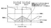
図1は、比較例の昇圧型のDC/DCコンバータのスイッチングトランジスタのゲートに印加される電圧SWの変化と、このインダクタに流れる電流ILの変化を示す図である。 FIG. 1 is a diagram showing a change in voltage SW applied to the gate of a switching transistor of a step-up DC / DC converter of a comparative example and a change in current IL flowing through the inductor.
図1に示すように、スイッチングトランジスタがオンするとインダクタに電流が流れてエネルギーが蓄えられる。このときの電流ILの変化は、式(1)にように表される。
スイッチングトランジスタがオフするとインダクタに蓄えられていたエネルギーが出力される。このときの電流ILの変化は、式(2)のように表される。
インダクタに流れた電流量Itotal(X+Y)のうち実際に出力電流Ioutとして出力端子2に出力されるのは、スイッチングトランジスタがオフしたときの電流量Yとなる。 Of the current amount Itotal (X + Y) flowing through the inductor, what is actually output to the
このように、スイッチングトランジスタがオン/オフする2つの状態の電流ILの変化が上述の式(1)、(2)のように表される。したがって、スイッチングトランジスタがオン/オフする割合ron:roffは、式(3)のように表される。
ron:roff=(Vout−Vin):Vin ・・・(3)
As described above, changes in the current IL in two states in which the switching transistor is turned on / off are expressed by the above-described equations (1) and (2). Therefore, the ratio ron: roff at which the switching transistor is turned on / off is expressed as in Expression (3).
ron: roff = (Vout−Vin): Vin (3)
これにより、以下の式(4)〜(6)が成り立つ。
したがって、式(4)〜(6)に示すように、出力電流Iout(出力電圧Vout)は、入力電圧Vinに比例した関係になる。なお、この式(4)で求められるIoutは、スイッチングトランジスタが1回オン/オフしている期間に、出力端子から出力される電流の平均値である。 Therefore, as shown in the equations (4) to (6), the output current Iout (output voltage Vout) is proportional to the input voltage Vin. In addition, Iout calculated | required by this Formula (4) is an average value of the electric current output from an output terminal in the period when the switching transistor is turned on / off once.
さらに、エラーアンプに入力される基準電圧は、入力電圧Vinから生成される。このため、基準電圧も入力電圧Vinに比例した影響を受けてしまう。 Further, the reference voltage input to the error amplifier is generated from the input voltage Vin. For this reason, the reference voltage is also affected in proportion to the input voltage Vin.
エラーアンプの入力である基準電圧Vrefと分圧電圧VFBは、どちらともVinの影響を受ける。このため、エラーアンプの出力も出力電圧Vinに比例することになる。 Both the reference voltage Vref and the divided voltage VFB that are inputs of the error amplifier are affected by Vin. For this reason, the output of the error amplifier is also proportional to the output voltage Vin.
このように、出力電流が変化すると出力電圧も変化してしまうため、出力電圧は入力電圧に比例した影響を受ける。そして、出力電圧は入力電圧の突然の変化に対して大きな影響を受ける。このとき、エラーアンプはレギュレーションを維持しようと制御する。しかし、出力電圧の変化が大きすぎるためエラーアンプの反応が追いつかず、出力電圧のLine Transient特性は大きく悪化し、出力電圧のリップルが大きくなる。 Thus, since the output voltage changes when the output current changes, the output voltage is affected in proportion to the input voltage. The output voltage is greatly affected by a sudden change in the input voltage. At this time, the error amplifier controls to maintain the regulation. However, since the change in the output voltage is too large, the response of the error amplifier cannot catch up, the Line Transient characteristic of the output voltage is greatly deteriorated, and the ripple of the output voltage is increased.
以上のように、比較例のDC/DCコンバータでは、入力電圧が変化すると出力電圧に大きなオーバーシュートやリンギングが生じてしまうという問題があった。 As described above, the DC / DC converter of the comparative example has a problem that when the input voltage changes, a large overshoot or ringing occurs in the output voltage.
そこで、本発明では、出力電圧に対する入力電圧の影響を低減することが可能なDC/DCコンバータを提案する。 Therefore, the present invention proposes a DC / DC converter that can reduce the influence of the input voltage on the output voltage.
以下、本発明に係る各実施例について図面に基づいて説明する。 Embodiments according to the present invention will be described below with reference to the drawings.
本実施例1では、特に、昇圧型のDC/DCコンバータの一例について説明する。 In the first embodiment, an example of a step-up DC / DC converter will be described.
図2は、本発明の一態様である実施例1に係るDC/DCコンバータ100の構成の一例を示す回路図である。 FIG. 2 is a circuit diagram showing an example of the configuration of the DC / DC converter 100 according to the first embodiment which is an aspect of the present invention.
図2に示すように、DC/DCコンバータ100は、入力端子1と、出力端子2と、インダクタ3と、スイッチングトランジスタ4と、ダイオード5と、コンデンサ6と、分圧回路7と、基準電圧生成回路8と、エラーアンプ9と、補償回路10と、フィードフォワード回路11と、乗算器12と、制御回路13と、ドライバ14と、を備える。 As shown in FIG. 2, the DC / DC converter 100 includes an
入力端子1は、直流電源(図示せず)に接続され、入力電圧Vinが入力されるようになっている。 The
出力端子2は、負荷15に接続され、この負荷15に出力電圧Voutを出力(供給)するようになっている。 The
インダクタ3は、入力端子1に一端が接続されている。 One end of the
スイッチングトランジスタ4は、インダクタ3の他端と接地GNDとの間に接続されている。このスイッチングトランジスタ4は、ここでは、nMOSトランジスタである。なお、このスイッチングトランジスタ4には、必要に応じて、信号の極性を適宜設定することにより、pMOSトランジスタやバイポーラトランジスタを用いてもよい。 The switching
ダイオード5は、インダクタ3の他端にアノードが接続され、カソードが出力端子2に接続されている。 The
コンデンサ6は、出力端子2と接地GNDとの間に接続されている。このコンデンサ6が充電されることにより出力端子2の電圧Voutが上昇し、一方、コンデンサ6が放電されることにより出力端子2の電圧Voutが下降する。 The capacitor 6 is connected between the
分圧回路7は、出力端子2と接地GNDとの間に接続されている。この分圧回路7は、出力電圧Voutを分圧した分圧電圧VFRを出力するようになっている。 The voltage dividing circuit 7 is connected between the
この分圧回路7は、出力端子2に一端が接続された第1の分圧抵抗7aと、この第1の分圧抵抗7aの他端と接地GNDとの間に接続された第2の分圧抵抗7bと、を有する。すなわち、分圧回路7は、これらの第1、第2の分圧抵抗7a、7bの分圧比で出力電圧Voutを分圧した分圧電圧VFRを出力する。 The voltage dividing circuit 7 includes a first
基準電圧生成回路8は、入力端子1と接地GNDとの間に接続されている。この基準電圧生成回路8は、入力電圧Vinに基づいて基準電圧Vrefを生成するようになっている。 The reference voltage generation circuit 8 is connected between the
エラーアンプ9は、分圧電圧VFBと前記基準電圧とが入力され、前記分圧電圧と前記基準電圧との差に応じた第1の信号Ierrを出力するようになっている。 The
補償回路10は、第1の信号Ierrの位相を調整するようになっている。 The
フィードフォワード回路11は、入力電圧Vinを検知し、この入力電圧Vinに反比例した電流に応じた第2の信号Ifeedを出力するようになっている。ここでは、第2の信号Ifeedは、電流Ic3と等価な信号である。 The
乗算器12は、第1の信号Ierrと第2の信号Ifeedとを乗算し、得られた第3の信号Isを出力するようになっている。 The
制御回路13は、第3の信号Isに基づいて、分圧電圧VFBと基準電圧Vrefとが等しくなるように、スイッチングトランジスタ4のオン/オフを制御するための制御信号Vcを出力するようになっている。例えば、制御回路13は、第3の信号Isのレベルが基準レベルよりも高くなったら、スイッチングトランジスタ4をオンする期間を長くし、また、第3の信号Isのレベルが基準レベルよりも低くなったら、スイッチングトランジスタ4をオンする期間を短くする。 Based on the third signal Is, the
ドライバ14は、制御回路13が出力した制御信号Vcを増幅してスイッチングトランジスタ4のゲートに印加するようになっている。 The
ここで、図3は、図2に示すDC/DCコンバータ100のフィードフォワード回路11の回路構成の一例を示す図である。 Here, FIG. 3 is a diagram showing an example of the circuit configuration of the
図3に示すように、フィードフォワード回路11は、第1の定電流源11aと、第1のトランジスタ11bと、第2のトランジスタ11cと、第2の定電流源11dと、第3のトランジスタ11eと、抵抗素子11fと、第4のトランジスタ11gと、第5のトランジスタ11hと、信号端子11iと、第6のトランジスタ11jと、を有する。 As shown in FIG. 3, the
第1の定電流源11aは、入力端子1に一端が接続されている。 One end of the first constant
第1のトランジスタ11bは、NPN型バイポーラトランジスタである。この第1のトランジスタ11bは、第1の定電流源11aの他端と接地GNDとの間に接続されている。この第1のトランジスタ11bには、電流Ic0が流れるようになっている。 The
第2のトランジスタ11cは、第1のトランジスタ11bと同一導電型のNPN型バイポーラトランジスタである。この第2のトランジスタ11cは、入力端子1に一端(コレクタ)が接続され、第1のトランジスタ11bの制御電極(ベース)に他端(エミッタ)が接続されている。この第2のトランジスタ11cには、電流Ic1が流れるようになっている。 The
第2の定電流源11dは、第2のトランジスタ11cの他端(エミッタ)と接地GNDとの間に接続されている。 The second constant
第3のトランジスタ11eは、第1のトランジスタ11bと同一導電型のNPN型バイポーラトランジスタである。この第3のトランジスタ11eは、入力端子1に一端(コレクタ)が接続され、第1のトランジスタ11bの一端(コレクタ)に制御電極(ベース)が接続されている。 The
抵抗素子11fは、入力端子1に一端が接続されている。この抵抗素子11fには、入力電圧Vinに比例した電流Irが流れるようになっている。 One end of the
第4のトランジスタ11gは、例えば、NPN型バイポーラトランジスタである。この第4のトランジスタ11gは、抵抗素子11fの他端と接地GNDとの間に接続されている。また、第4のトランジスタ11gは、ダイオード接続されている。 The
第5のトランジスタ11hは、例えば、NPN型バイポーラトランジスタである。この第5のトランジスタ11hは、第3のトランジスタ11eの他端(エミッタ)と接地GNDとの間に接続されている。 The
すなわち、第4のトランジスタ11gと第5のトランジスタ11hとは、ミラー回路を構成する。これにより、第5のトランジスタ11hには、第4のトランジスタ11gに流れる電流Irをミラーした電流Ic2が流れる。 That is, the
これにより、電流Ic2は、入力電圧Vinに比例することになる。 As a result, the current Ic2 is proportional to the input voltage Vin.
また、信号端子11iは、乗算器12の入力に接続されており、第2の信号Ifeedを出力するようになっている。 The
第6のトランジスタ11jは、例えば、NPN型バイポーラトランジスタである。この第6のトランジスタ11jは、信号端子11iと接地GNDとの間に接続され、第3のトランジスタ11eの他端(エミッタ)に制御電極(ベース)が接続されている。 The
この第6のトランジスタ11jには、後述のように、電流Ic2に反比例する電流Ic3が流れるようになっている。この電流Ic3が、第2の信号Ifeedに相当する。 As will be described later, a current Ic3 that is inversely proportional to the current Ic2 flows through the
ここで、上記構成を有するDC/DCコンバータ100の出力特性について検討する。 Here, the output characteristics of the DC / DC converter 100 having the above-described configuration will be examined.
まず、フィードフォワード回路11の第1〜第3、第6のトランジスタ11b、11c、11e、11jのベース・エミッタ間電圧の関係は、式(7)のように表される。
一般的に、ベース電圧VBEは、式(8)のように表される。なお、式(8)において、qは単位電子電荷であり、kはボルツマン定数であり、tは絶対温度である。
したがって、式(7)、式(8)より、電流Ic0〜Ic3の関係は、以下の式(9)のように表される。
この式(9)を変形することにより、電流Ic3は、式(10)のように表される。
既述のように、電流Irは、入力電圧Vinに比例する。したがって、第4、第5のトランジスタ11g、11hのカレントミラーにより、電流Ic2は、入力電圧Vinに比例した電流となる。 As described above, the current Ir is proportional to the input voltage Vin. Therefore, the current Ic2 becomes a current proportional to the input voltage Vin by the current mirrors of the fourth and
電流Ic0、Ic1は定電流であるので、式(10)より、電流Ic3は、入力電圧Vinに反比例した電流となる。 Since the currents Ic0 and Ic1 are constant currents, the current Ic3 is a current inversely proportional to the input voltage Vin according to the equation (10).
ここで、図4Aは、図2に示すDC/DCコンバータ100の入力端子1に入力される入力電圧Vinの波形を示す図である。また、図4Bは、図2に示すDC/DCコンバータ100のフィードフォワード回路11に流れる電流Ic2の波形を示す図である。また、図4Cは、図2に示すDC/DCコンバータ100のフィードフォワード回路11に流れる電流Ic3の波形を示す図である。 Here, FIG. 4A is a diagram showing a waveform of the input voltage Vin input to the
図4Aないし図4Cに示すように、電流Ic3は、入力電圧Vin(すなわち、電流Ic2)に対して反比例するシミュレート結果が得られた。 As shown in FIGS. 4A to 4C, a simulation result is obtained in which the current Ic3 is inversely proportional to the input voltage Vin (ie, the current Ic2).
既述のように、フィードフォワード回路11は、入力電圧Vinを検知し、この入力電圧Vinに反比例した電流Ic3に応じた第2の信号Ifeedを出力するようになっている。また、ここでは、第2の信号Ifeedは、電流Ic3と等価な信号である。 As described above, the
そして、既述のように乗算器12により、入力電圧Vinに反比例した信号Ifeedがエラーアンプの出力に乗算され、乗算された結果が信号Isとなる。この信号Isは、入力電圧Vinの既述の影響が相殺されている。この信号Isに基づいて、制御回路13は、スイッチングトランジスタ4を制御することになる。 As described above, the
すなわち、既述の式(6)の右辺に、入力電圧Vinに反比例する項が乗算される形となり、入力電圧Vinが打ち消される。これにより、DC/DCコンバータ100は、出力電流Iout(出力電圧Vout)がVinの影響を受けない状態にすることが可能となる。 In other words, the right side of the above-described equation (6) is multiplied by a term inversely proportional to the input voltage Vin, and the input voltage Vin is canceled. Thus, the DC / DC converter 100 can make the output current Iout (output voltage Vout) not affected by Vin.
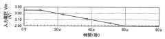
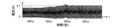
ここで、図5Aは、図2に示すDC/DCコンバータ100の入力電圧Vinの波形を示す図である。また、図5Bは、図2に示すDC/DCコンバータ100のインダクタ3に流れる電流の波形を示す図である。また、図5Cは、図2に示すDC/DCコンバータ100の出力電圧Voutの波形を示す図である。 Here, FIG. 5A is a diagram showing a waveform of the input voltage Vin of the DC / DC converter 100 shown in FIG. FIG. 5B is a diagram showing a waveform of a current flowing through the
図5Aないし図5Cに示すように、入力電圧Vinを3.7Vから3.2Vに50μ秒かけて変化させたときの出力電圧Voutの変化(オーバーシュート)が、6.8mVとなっている。なお、同様の条件で、比較例の構成では、出力電圧Voutの変化(オーバーシュート)が、260mVであった。 As shown in FIGS. 5A to 5C, the change (overshoot) of the output voltage Vout when the input voltage Vin is changed from 3.7 V to 3.2 V over 50 μs is 6.8 mV. Under the same conditions, in the configuration of the comparative example, the change (overshoot) in the output voltage Vout was 260 mV.
このように、本実施例1に係るDC/DCコンバータ100は、入力電圧Vinを急激に変化した場合でも、比較例よりもLine Transient特性が大きく改善され、オーバーシュートが小さくなっている。 As described above, in the DC / DC converter 100 according to the first embodiment, even when the input voltage Vin is suddenly changed, the line transient characteristics are greatly improved and the overshoot is smaller than that in the comparative example.
以上のように、本実施例に係るDC/DCコンバータによれば、出力電圧に対する入力電圧の影響を低減することができる。 As described above, according to the DC / DC converter according to the present embodiment, the influence of the input voltage on the output voltage can be reduced.
実施例1では、昇圧型のDC/DCコンバータの一例について説明した。 In the first embodiment, an example of a step-up DC / DC converter has been described.
ここで、本発明は、反転型のDC/DCコンバータにも適用することができる。 Here, the present invention can also be applied to an inverting DC / DC converter.
この反転型のDC/DCコンバータは、スイッチングトランジスタをオンするとインダクタにエネルギーが蓄えられる。そして、このDC/DCコンバータは、スイッチングトランジスタをオフすると蓄えられていたエネルギーを流そうとして出力端子に接続されたコンデンサ・ダイオードを通して電流が流れ出力コンデンサに電荷がチャージされる。このとき、出力コンデンサの接地側が正となるため、出力に負の電圧を出力することが可能となる。 In this inverting DC / DC converter, when the switching transistor is turned on, energy is stored in the inductor. In the DC / DC converter, when the switching transistor is turned off, a current flows through a capacitor / diode connected to the output terminal so as to flow the stored energy, and the output capacitor is charged. At this time, since the ground side of the output capacitor is positive, a negative voltage can be output to the output.
ここで、図6は、比較例となる反転型のDC/DCコンバータのスイッチングトランジスタのゲートに印加される電圧SWの変化と、このインダクタに流れる電流ILの変化を示す図である。 Here, FIG. 6 is a diagram showing a change in the voltage SW applied to the gate of the switching transistor of the inverting DC / DC converter as a comparative example and a change in the current IL flowing through the inductor.
既述のように、スイッチングトランジスタがオンするとインダクタにエネルギーが蓄えられる。このときの電流ILの変化は、式(11)のように表される。
そして、スイッチングトランジスタがオフすると蓄えられていたエネルギーが出力される。このときの電流ILの変化は、式(12)のように表される。
また、昇圧型と同様に、インダクタに流れた電流量Itotal(X+Y)のうち実際に出力電流Ioutとして出力端子2に出力されるのは、スイッチングトランジスタがオフしたときの電流量Yとなる。 Similarly to the step-up type, the current amount Itotal (X + Y) flowing through the inductor is actually output to the
このように、スイッチングトランジスタがオン/オフする2つの状態の電流ILの変化が上述の式(11)、(12)のように表される。したがって、スイッチングトランジスタがオン/オフする割合ron:roffは、式(3)のように表される。
ron:roff=Vout:Vin ・・・(13)
In this way, changes in the current IL in two states in which the switching transistor is turned on / off are expressed by the above-described equations (11) and (12). Therefore, the ratio ron: roff at which the switching transistor is turned on / off is expressed as in Expression (3).
ron: roff = Vout: Vin (13)
これにより、以下の式(14)〜(16)が成り立つ。
したがって、式(14)〜(16)に示すように、出力電流Iout(出力電圧Vout)は、入力電圧Vinに比例した関係になる。なお、この式(14)で求められるIoutは、スイッチングトランジスタが1回オン/オフしている期間に、出力端子から出力される電流の平均値である。 Therefore, as shown in the equations (14) to (16), the output current Iout (output voltage Vout) has a relationship proportional to the input voltage Vin. In addition, Iout calculated | required by this Formula (14) is an average value of the electric current output from an output terminal in the period when the switching transistor is turned on / off once.
これにより、昇圧型のDC/DCコンバータと同様に、反転型のDC/DCコンバータでも、入力電圧が変化すると出力電圧に大きなオーバーシュートやリンギングが生じてしまう。 As a result, as with the step-up DC / DC converter, even with the inverting DC / DC converter, when the input voltage changes, a large overshoot or ringing occurs in the output voltage.
そこで、本実施例2では、出力電圧に対する入力電圧の影響を低減することが可能な反転型のDC/DCコンバータの一例について説明する。 In the second embodiment, an example of an inverting DC / DC converter that can reduce the influence of the input voltage on the output voltage will be described.
図7は、本発明の一態様である実施例2に係るDC/DCコンバータ200の構成の一例を示す回路図である。 FIG. 7 is a circuit diagram showing an example of the configuration of a DC / DC converter 200 according to a second embodiment which is an aspect of the present invention.
図7に示すように、DC/DCコンバータ200は、入力端子1と、出力端子2と、インダクタ3aと、スイッチングトランジスタ4aと、ダイオード5aと、コンデンサ6と、分圧回路7と、基準電圧生成回路8と、エラーアンプ9と、補償回路10と、フィードフォワード回路11と、乗算器12と、制御回路13と、ドライバ14と、を備える。 As shown in FIG. 7, the DC / DC converter 200 includes an
なお、図7に示す反転型のDC/DCコンバータ200は、図2に示す昇圧型のDC/DCコンバータ100と比較して、インダクタ3a、スイッチングトランジスタ4a、および、ダイオード5aの構成・接続関係が異なる以外は、同様の構成である。 7 is different from the step-up DC / DC converter 100 shown in FIG. 2 in the configuration and connection relationship of the
スイッチングトランジスタ4aは、入力端子1に一端(ソース)接続されている。このスイッチングトランジスタ4aは、ここでは、pMOSトランジスタである。なお、このスイッチングトランジスタ4aには、必要に応じて、信号の極性を適宜設定することにより、nMOSトランジスタやバイポーラトランジスタを用いてもよい。 The switching
インダクタ3aは、スイッチングトランジスタ4aの他端(ドレイン)と接地GNDとの間に接続されている。 The
ダイオード5aは、スイッチングトランジスタ4aの他端(ドレイン)にカソードが接続され、出力端子2にアノード接続されている。 The
制御回路13は、第3の信号Isに基づいて、分圧電圧VFBと基準電圧Vrefとが等しくなるように、スイッチングトランジスタ4aのオン/オフを制御するための制御信号Vcを出力するようになっている。例えば、制御回路13は、第3の信号Isのレベルが基準レベルよりも高くなったら、スイッチングトランジスタ4aをオンする期間を長くし、また、第3の信号Isのレベルが基準レベルよりも低くなったら、スイッチングトランジスタ4aをオンする期間を短くする。 Based on the third signal Is, the
ドライバ14は、制御回路13が出力した制御信号Vcを増幅してスイッチングトランジスタ4aのゲートに印加するようになっている。 The
ここで、上記構成を有する反転型のDC/DCコンバータ100の出力特性は、既述の昇圧型のDC/DCコンバータと同様である。 Here, the output characteristics of the inverting DC / DC converter 100 having the above-described configuration are the same as those of the step-up DC / DC converter described above.
すなわち、実施例1と同様に、フィードフォワード回路11は、入力電圧Vinを検知し、この入力電圧Vinに反比例した電流Ic3に応じた第2の信号Ifeedを出力するようになっている。 That is, as in the first embodiment, the
そして、既述のように乗算器12により、入力電圧Vinに反比例した信号Ifeedがエラーアンプの出力に乗算され、乗算された結果が信号Isとなる。この信号Isは、入力電圧Vinの既述の影響が相殺されている。この信号Isに基づいて、制御回路13は、スイッチングトランジスタ4を制御することになる。 As described above, the
すなわち、実施例1と同様に、DC/DCコンバータ200は、出力電流Iout(出力電圧Vout)がVinの影響を受けない状態にすることが可能となる。 That is, as in the first embodiment, the DC / DC converter 200 can make the output current Iout (output voltage Vout) unaffected by Vin.
以上のように、本実施例に係るDC/DCコンバータによれば、出力電圧に対する入力電圧の影響を低減することができる。 As described above, according to the DC / DC converter according to the present embodiment, the influence of the input voltage on the output voltage can be reduced.
なお、以上の各実施例においては、フィードフォワード回路11を構成するトランジスタをNPN型バイポーラトランジスタで構成した場合について説明した。 In each of the above-described embodiments, the case where the transistors constituting the
しかし、フィードフォワード回路11を構成するトランジスタをPNP型バイポーラトランジスタや、MOSトランジスタで構成してもよい。 However, the transistors constituting the
1 入力端子
2 出力端子
3 インダクタ
4 スイッチングトランジスタ
5 ダイオード
6 コンデンサ
7 分圧回路
7a 第1の分圧抵抗
7b 第2の分圧抵抗
8 基準電圧生成回路
9 エラーアンプ
10 補償回路
11 フィードフォワード回路
11a 第1の定電流源
11b 第1のトランジスタ
11c 第2のトランジスタ
11d 第2の定電流源
11e 第3のトランジスタ
11f 抵抗素子
11g 第4のトランジスタ
11h 第5のトランジスタ
11i 信号端子
11j 第6のトランジスタ
12 乗算器
13 制御回路
14 ドライバ
15 負荷
100、200 DC/DCコンバータ
11 Feed
Claims (5)
Translated fromJapanese直流電源が接続されるようになっており、入力電圧が入力される入力端子と、
負荷が接続されるようになっており、出力電圧を出力する出力端子と、
前記入力端子に一端が接続されたインダクタと、
前記インダクタの他端と接地との間に接続されたスイッチングトランジスタと、
前記インダクタの他端にアノードが接続され、前記出力端子にカソードが接続されたダイオードと、
前記出力端子と前記接地との間に接続されたコンデンサと、
前記出力端子と前記接地との間に接続され、前記出力電圧を分圧した分圧電圧を出力する分圧回路と、
前記入力電圧に基づいて基準電圧を生成する基準電圧生成回路と、
前記分圧電圧と前記基準電圧とが入力され、前記分圧電圧と前記基準電圧との差に応じた第1の信号を出力するエラーアンプと、
前記入力電圧を検知し、この入力電圧に反比例した電流に応じた第2の信号を出力するフィードフォワード回路と、
前記第1の信号と前記第2の信号とを乗算し、得られた第3の信号を出力する乗算器と、
前記第3の信号に基づいて、前記分圧電圧と前記基準電圧とが等しくなるように、前記スイッチングトランジスタのオン/オフを制御するための制御信号を出力する制御回路と、を備える
ことを特徴とするDC/DCコンバータ。A step-up DC / DC converter,
A DC power supply is connected, and an input terminal to which an input voltage is input,
A load is connected, and an output terminal that outputs an output voltage;
An inductor having one end connected to the input terminal;
A switching transistor connected between the other end of the inductor and ground;
A diode having an anode connected to the other end of the inductor and a cathode connected to the output terminal;
A capacitor connected between the output terminal and the ground;
A voltage dividing circuit which is connected between the output terminal and the ground and outputs a divided voltage obtained by dividing the output voltage;
A reference voltage generation circuit that generates a reference voltage based on the input voltage;
An error amplifier that receives the divided voltage and the reference voltage and outputs a first signal corresponding to a difference between the divided voltage and the reference voltage;
A feedforward circuit that detects the input voltage and outputs a second signal corresponding to a current inversely proportional to the input voltage;
A multiplier for multiplying the first signal by the second signal and outputting a third signal obtained;
A control circuit that outputs a control signal for controlling on / off of the switching transistor so that the divided voltage and the reference voltage are equal to each other based on the third signal. DC / DC converter.
入力電圧が入力される入力端子と、
出力電圧を出力する出力端子と、
前記入力端子に一端が接続されたインダクタと、
前記インダクタの他端と接地との間に接続されたスイッチングトランジスタと、
前記インダクタの他端にアノードが接続され、前記出力端子にカソードが接続されたダイオードと、
前記出力端子と前記接地との間に接続されたコンデンサと、
前記出力端子と前記接地との間に接続され、前記出力電圧を分圧した分圧電圧を出力する分圧回路と、
前記入力電圧に基づいて基準電圧を生成する基準電圧生成回路と、
前記分圧電圧と前記基準電圧とが入力され、前記分圧電圧と前記基準電圧との差に応じた第1の信号を出力するエラーアンプと、
前記入力電圧を検知し、この入力電圧に反比例した電流に応じた第2の信号を出力するフィードフォワード回路と、
前記第1の信号と前記第2の信号とを乗算し、得られた第3の信号を出力する乗算器と、
前記第3の信号に基づいて、前記分圧電圧と前記基準電圧とが等しくなるように、前記スイッチングトランジスタのオン/オフを制御するための制御信号を出力する制御回路と、を備え、
前記フィードフォワード回路は、
前記入力端子に一端が接続された第1の定電流源と、
前記第1の定電流源の他端と接地との間に接続された第1のトランジスタと、
前記入力端子に一端が接続され、前記第1のトランジスタの制御電極に他端が接続され、 前記第1のトランジスタと同一導電型の第2のトランジスタと、
前記第2のトランジスタの他端と接地との間に接続された第2の定電流源と、
前記入力端子に一端が接続され、前記第1のトランジスタの一端に制御電極が接続され、 前記第1のトランジスタと同一導電型の第3のトランジスタと、
前記入力端子に一端が接続された抵抗素子と、
前記抵抗素子の他端と前記接地との間に接続された第4のトランジスタと、
前記第3のトランジスタの他端と前記接地との間に接続され、前記第4のトランジスタに流れる電流をミラーした電流が流れる第5のトランジスタと、
前記第2の信号を出力するための信号端子と、
前記信号端子と前記接地との間に接続され、前記第3のトランジスタの他端に制御電極が接続された第6のトランジスタと、を有する
ことを特徴とするDC/DCコンバータ。A step-up DC / DC converter,
An input terminal to which an input voltage is input;
An output terminal for outputting an output voltage;
An inductor having one end connected to the input terminal;
A switching transistor connected between the other end of the inductor and ground;
A diode having an anode connected to the other end of the inductor and a cathode connected to the output terminal;
A capacitor connected between the output terminal and the ground;
A voltage dividing circuit which is connected between the output terminal and the ground and outputs a divided voltage obtained by dividing the output voltage;
A reference voltage generation circuit that generates a reference voltage based on the input voltage;
An error amplifier that receives the divided voltage and the reference voltage and outputs a first signal corresponding to a difference between the divided voltage and the reference voltage;
A feedforward circuit that detects the input voltage and outputs a second signal corresponding to a current inversely proportional to the input voltage;
A multiplier for multiplying the first signal by the second signal and outputting a third signal obtained;
A control circuit that outputs a control signal for controlling on / off of the switching transistor so that the divided voltage and the reference voltage are equal to each other based on the third signal;
The feedforward circuit is
A first constant current source having one end connected to the input terminal;
A first transistor connected between the other end of the first constant current source and ground;
One end connected to the input terminal, the other end connected to the control electrode of the first transistor, a second transistor of the same conductivity type as the first transistor;
A second constant current source connected between the other end of the second transistor and ground;
One end connected to the input terminal, a control electrode connected to one end of the first transistor, a third transistor of the same conductivity type as the first transistor;
A resistance element having one end connected to the input terminal;
A fourth transistor connected between the other end of the resistance element and the ground;
A fifth transistor connected between the other end of the third transistor and the ground, and through which a current that mirrors a current flowing through the fourth transistor flows;
A signal terminal for outputting the second signal;
A DC / DC converter comprising: a sixth transistor connected between the signal terminal and the ground and having a control electrode connected to the other end of the third transistor.
入力電圧が入力される入力端子と、
出力電圧を出力する出力端子と、
前記入力端子に一端が接続されたスイッチングトランジスタと、
前記スイッチングトランジスタの他端と接地との間に接続されたインダクタと、
前記スイッチングトランジスタの他端にカソードが接続され、前記出力端子にアノードが接続されたダイオードと、
前記出力端子と前記接地との間に接続されたコンデンサと、
前記出力端子と前記接地との間に接続され、前記出力電圧を分圧した分圧電圧を出力する分圧回路と、
前記入力電圧に基づいて基準電圧を生成する基準電圧生成回路と、
前記分圧電圧と前記基準電圧とが入力され、前記分圧電圧と前記基準電圧との差に応じた第1の信号を出力するエラーアンプと、
前記入力電圧を検知し、この入力電圧に反比例した電流に応じた第2の信号を出力するフィードフォワード回路と、
前記第1の信号と前記第2の信号とを乗算し、得られた第3の信号を出力する乗算器と、
前記第3の信号に基づいて、前記分圧電圧と前記基準電圧とが等しくなるように、前記スイッチングトランジスタのオン/オフを制御するための制御信号を出力する制御回路と、を備える
ことを特徴とするDC/DCコンバータ。An inverting DC / DC converter,
An input terminal to which an input voltage is input;
An output terminal for outputting an output voltage;
A switching transistor having one end connected to the input terminal;
An inductor connected between the other end of the switching transistor and ground;
A diode having a cathode connected to the other end of the switching transistor and an anode connected to the output terminal;
A capacitor connected between the output terminal and the ground;
A voltage dividing circuit which is connected between the output terminal and the ground and outputs a divided voltage obtained by dividing the output voltage;
A reference voltage generation circuit that generates a reference voltage based on the input voltage;
An error amplifier that receives the divided voltage and the reference voltage and outputs a first signal corresponding to a difference between the divided voltage and the reference voltage;
A feedforward circuit that detects the input voltage and outputs a second signal corresponding to a current inversely proportional to the input voltage;
A multiplier for multiplying the first signal by the second signal and outputting a third signal obtained;
A control circuit that outputs a control signal for controlling on / off of the switching transistor so that the divided voltage and the reference voltage are equal to each other based on the third signal. DC / DC converter.
Priority Applications (2)
| Application Number | Priority Date | Filing Date | Title |
|---|---|---|---|
| JP2008217068AJP4818334B2 (en) | 2008-08-26 | 2008-08-26 | DC / DC converter |
| US12/547,050US8207722B2 (en) | 2008-08-26 | 2009-08-25 | DC/DC converter |
Applications Claiming Priority (1)
| Application Number | Priority Date | Filing Date | Title |
|---|---|---|---|
| JP2008217068AJP4818334B2 (en) | 2008-08-26 | 2008-08-26 | DC / DC converter |
Publications (2)
| Publication Number | Publication Date |
|---|---|
| JP2010057222A JP2010057222A (en) | 2010-03-11 |
| JP4818334B2true JP4818334B2 (en) | 2011-11-16 |
Family
ID=41724344
Family Applications (1)
| Application Number | Title | Priority Date | Filing Date |
|---|---|---|---|
| JP2008217068AExpired - Fee RelatedJP4818334B2 (en) | 2008-08-26 | 2008-08-26 | DC / DC converter |
Country Status (2)
| Country | Link |
|---|---|
| US (1) | US8207722B2 (en) |
| JP (1) | JP4818334B2 (en) |
Families Citing this family (15)
| Publication number | Priority date | Publication date | Assignee | Title |
|---|---|---|---|---|
| JP5513829B2 (en) | 2009-10-01 | 2014-06-04 | パナソニック株式会社 | Current drive circuit |
| CN101951149B (en)* | 2010-08-05 | 2013-02-27 | 复旦大学 | A Frequency Control Circuit Suitable for Constant Off-time Controlled Boost Converter |
| US9030050B1 (en)* | 2010-11-26 | 2015-05-12 | Senseg Ltd. | Voltage amplifier |
| JP5550591B2 (en)* | 2011-03-28 | 2014-07-16 | 株式会社東芝 | Switching power supply control method and switching power supply at light load or no load |
| JP2014112988A (en)* | 2012-12-05 | 2014-06-19 | Sanken Electric Co Ltd | Switching power-supply device |
| CN103166464B (en)* | 2013-03-29 | 2016-09-07 | 株式会社村田制作所 | Power converter and method for power conversion |
| GB2522201B (en)* | 2014-01-15 | 2018-06-27 | Nidec Control Techniques Ltd | Method and system for controlling a power output of an inverter |
| JP6097237B2 (en)* | 2014-03-10 | 2017-03-15 | 株式会社東芝 | DC-DC converter and semiconductor integrated circuit |
| CN204068695U (en)* | 2014-06-13 | 2014-12-31 | 株式会社村田制作所 | Power conversion system |
| JP6153144B1 (en)* | 2016-03-17 | 2017-06-28 | 三菱電機株式会社 | Control device and control method for DC / DC converter |
| US10181791B2 (en) | 2017-04-14 | 2019-01-15 | Allegro Microsystems, Llc | Converter digital control circuit with adaptive compensation |
| US10386882B2 (en)* | 2017-04-14 | 2019-08-20 | Allegro Microsystems, Llc | Control circuit |
| CN109545123A (en)* | 2019-01-07 | 2019-03-29 | 合肥京东方显示技术有限公司 | Voltage compensating circuit, its voltage compensating method, drive system and display device |
| US11469666B2 (en)* | 2019-10-01 | 2022-10-11 | Allegro Microsystems, Llc | Converter digital control circuit with adaptive feedforward compensation |
| JP2022141252A (en) | 2021-03-15 | 2022-09-29 | 横河電機株式会社 | boost circuit |
Family Cites Families (9)
| Publication number | Priority date | Publication date | Assignee | Title |
|---|---|---|---|---|
| US5708356A (en)* | 1995-08-04 | 1998-01-13 | Kabushiki Kaisha Toshiba | Apparatus for supplying stabilized power to a load having voltage-current characteristics exhibiting partial negative resistance |
| KR100206143B1 (en)* | 1996-08-28 | 1999-07-01 | 윤종용 | High power factor compensation circuit |
| JP4725696B2 (en)* | 2001-05-31 | 2011-07-13 | サンケン電気株式会社 | Switching power supply |
| JP4386746B2 (en) | 2004-01-27 | 2009-12-16 | 新日本無線株式会社 | Step-up switching regulator |
| US20060043942A1 (en)* | 2004-05-13 | 2006-03-02 | Isaac Cohen | Power converter apparatus and methods using output current feedforward control |
| US7317625B2 (en)* | 2004-06-04 | 2008-01-08 | Iwatt Inc. | Parallel current mode control using a direct duty cycle algorithm with low computational requirements to perform power factor correction |
| JP4932584B2 (en)* | 2005-11-25 | 2012-05-16 | 株式会社リコー | Synchronous rectification type switching regulator |
| US7313007B2 (en)* | 2006-04-20 | 2007-12-25 | Tsai-Fu Wu | Power factor correction controller |
| JP4931129B2 (en)* | 2007-01-29 | 2012-05-16 | 東芝三菱電機産業システム株式会社 | Power converter |
- 2008
- 2008-08-26JPJP2008217068Apatent/JP4818334B2/ennot_activeExpired - Fee Related
- 2009
- 2009-08-25USUS12/547,050patent/US8207722B2/ennot_activeExpired - Fee Related
Also Published As
| Publication number | Publication date |
|---|---|
| US20100052627A1 (en) | 2010-03-04 |
| US8207722B2 (en) | 2012-06-26 |
| JP2010057222A (en) | 2010-03-11 |
Similar Documents
| Publication | Publication Date | Title |
|---|---|---|
| JP4818334B2 (en) | DC / DC converter | |
| US10075073B2 (en) | DC/DC converter and switching power supply having overcurrent protection | |
| JP5332248B2 (en) | Power supply | |
| KR100967474B1 (en) | Switching regulators and electronics with them | |
| US20050007167A1 (en) | PWM switching regulator control circuit | |
| JP5513778B2 (en) | Switching power supply circuit | |
| JP2013153563A (en) | Semiconductor integrated circuit device and dc-dc converter | |
| TW201444242A (en) | DC-DC converter controller | |
| JP2015130744A (en) | Power circuit | |
| JP5642349B2 (en) | Pulse width modulation circuit, pulse width modulation method and regulator | |
| US20180316265A1 (en) | Boost dc-dc converter having digital control and reference pwm generators | |
| JP6160188B2 (en) | Switching regulator | |
| KR20060049915A (en) | DC-DC converter circuit | |
| JP2015012694A (en) | Power circuit | |
| JP5514460B2 (en) | Input current limiting circuit and power supply device using the same | |
| JP2012016123A (en) | Dc-dc converter | |
| JP2009153249A (en) | DC-DC converter | |
| JP2010226821A (en) | Output current limiting circuit and power unit using the same | |
| JP2010283999A (en) | Power supply device, control circuit, and control method for power supply device | |
| JP2011030391A (en) | Power supply unit | |
| JP7381397B2 (en) | power supply | |
| JP6177813B2 (en) | DC-DC converter | |
| JP2012034472A (en) | Power supply control circuit and power supply circuit | |
| JP5094512B2 (en) | Switching regulator | |
| JP2009171670A (en) | Power supply circuit and power supply system |
Legal Events
| Date | Code | Title | Description |
|---|---|---|---|
| A621 | Written request for application examination | Free format text:JAPANESE INTERMEDIATE CODE: A621 Effective date:20100804 | |
| A977 | Report on retrieval | Free format text:JAPANESE INTERMEDIATE CODE: A971007 Effective date:20101118 | |
| A131 | Notification of reasons for refusal | Free format text:JAPANESE INTERMEDIATE CODE: A131 Effective date:20101130 | |
| A521 | Written amendment | Free format text:JAPANESE INTERMEDIATE CODE: A523 Effective date:20110128 | |
| TRDD | Decision of grant or rejection written | ||
| A01 | Written decision to grant a patent or to grant a registration (utility model) | Free format text:JAPANESE INTERMEDIATE CODE: A01 Effective date:20110802 | |
| A01 | Written decision to grant a patent or to grant a registration (utility model) | Free format text:JAPANESE INTERMEDIATE CODE: A01 | |
| A61 | First payment of annual fees (during grant procedure) | Free format text:JAPANESE INTERMEDIATE CODE: A61 Effective date:20110830 | |
| FPAY | Renewal fee payment (event date is renewal date of database) | Free format text:PAYMENT UNTIL: 20140909 Year of fee payment:3 | |
| R151 | Written notification of patent or utility model registration | Ref document number:4818334 Country of ref document:JP Free format text:JAPANESE INTERMEDIATE CODE: R151 | |
| FPAY | Renewal fee payment (event date is renewal date of database) | Free format text:PAYMENT UNTIL: 20140909 Year of fee payment:3 | |
| LAPS | Cancellation because of no payment of annual fees |