JP4817210B2 - Film forming apparatus and film forming method - Google Patents
Film forming apparatus and film forming methodDownload PDFInfo
- Publication number
- JP4817210B2 JP4817210B2JP2001000183AJP2001000183AJP4817210B2JP 4817210 B2JP4817210 B2JP 4817210B2JP 2001000183 AJP2001000183 AJP 2001000183AJP 2001000183 AJP2001000183 AJP 2001000183AJP 4817210 B2JP4817210 B2JP 4817210B2
- Authority
- JP
- Japan
- Prior art keywords
- process gas
- gas
- support member
- substrate
- gas discharge
- Prior art date
- Legal status (The legal status is an assumption and is not a legal conclusion. Google has not performed a legal analysis and makes no representation as to the accuracy of the status listed.)
- Expired - Fee Related
Links
- 238000000034methodMethods0.000titleclaimsdescription145
- 239000000758substrateSubstances0.000claimsdescription103
- 238000010926purgeMethods0.000claimsdescription75
- 238000007599dischargingMethods0.000claimsdescription21
- 238000010438heat treatmentMethods0.000claimsdescription20
- 238000004140cleaningMethods0.000claimsdescription11
- 230000015572biosynthetic processEffects0.000claimsdescription6
- 150000001875compoundsChemical class0.000claimsdescription6
- 238000001179sorption measurementMethods0.000claimsdescription5
- 229910052719titaniumInorganic materials0.000claimsdescription5
- 229910004541SiNInorganic materials0.000claimsdescription4
- 229910004166TaNInorganic materials0.000claimsdescription4
- 238000000151depositionMethods0.000claimsdescription4
- 229910052707rutheniumInorganic materials0.000claimsdescription4
- 229910052710siliconInorganic materials0.000claimsdescription4
- 229910052814silicon oxideInorganic materials0.000claimsdescription4
- 229910052715tantalumInorganic materials0.000claimsdescription4
- 229910052721tungstenInorganic materials0.000claimsdescription4
- 229910052726zirconiumInorganic materials0.000claimsdescription4
- 229910020177SiOFInorganic materials0.000claimsdescription3
- ATJFFYVFTNAWJD-UHFFFAOYSA-NTinChemical compound[Sn]ATJFFYVFTNAWJD-UHFFFAOYSA-N0.000claimsdescription3
- 229910052782aluminiumInorganic materials0.000claimsdescription3
- 230000008021depositionEffects0.000claimsdescription3
- 229910052718tinInorganic materials0.000claimsdescription3
- 229910018072Al 2 O 3Inorganic materials0.000claims2
- 229910004298SiO 2Inorganic materials0.000claims2
- 239000012528membraneSubstances0.000claims2
- 239000007789gasSubstances0.000description292
- 235000012431wafersNutrition0.000description73
- 239000010408filmSubstances0.000description50
- 239000010410layerSubstances0.000description22
- NRTOMJZYCJJWKI-UHFFFAOYSA-NTitanium nitrideChemical compound[Ti]#NNRTOMJZYCJJWKI-UHFFFAOYSA-N0.000description15
- 238000005229chemical vapour depositionMethods0.000description14
- 229910003074TiCl4Inorganic materials0.000description12
- 238000000231atomic layer depositionMethods0.000description10
- 239000010936titaniumSubstances0.000description10
- 150000002736metal compoundsChemical class0.000description7
- 229910020323ClF3Inorganic materials0.000description6
- 239000002356single layerSubstances0.000description6
- 239000004065semiconductorSubstances0.000description5
- VYPSYNLAJGMNEJ-UHFFFAOYSA-NSilicium dioxideChemical compoundO=[Si]=OVYPSYNLAJGMNEJ-UHFFFAOYSA-N0.000description4
- 239000010409thin filmSubstances0.000description4
- MCMNRKCIXSYSNV-UHFFFAOYSA-NZrO2Inorganic materialsO=[Zr]=OMCMNRKCIXSYSNV-UHFFFAOYSA-N0.000description3
- 238000005240physical vapour depositionMethods0.000description3
- 239000012159carrier gasSubstances0.000description2
- 229910052681coesiteInorganic materials0.000description2
- 229910052906cristobaliteInorganic materials0.000description2
- WOCIAKWEIIZHES-UHFFFAOYSA-Nruthenium(IV) oxideInorganic materialsO=[Ru]=OWOCIAKWEIIZHES-UHFFFAOYSA-N0.000description2
- 238000000926separation methodMethods0.000description2
- 239000000377silicon dioxideSubstances0.000description2
- 229910052682stishoviteInorganic materials0.000description2
- 229910052905tridymiteInorganic materials0.000description2
- 229910007264Si2H6Inorganic materials0.000description1
- 229910003910SiCl4Inorganic materials0.000description1
- 229910003818SiH2Cl2Inorganic materials0.000description1
- BLRPTPMANUNPDV-UHFFFAOYSA-NSilaneChemical compound[SiH4]BLRPTPMANUNPDV-UHFFFAOYSA-N0.000description1
- -1Ta (OC2H5)5Chemical compound0.000description1
- 229910008484TiSiInorganic materials0.000description1
- 229910009035WF6Inorganic materials0.000description1
- 230000004888barrier functionEffects0.000description1
- PZPGRFITIJYNEJ-UHFFFAOYSA-NdisilaneChemical compound[SiH3][SiH3]PZPGRFITIJYNEJ-UHFFFAOYSA-N0.000description1
- 230000000694effectsEffects0.000description1
- 239000012530fluidSubstances0.000description1
- 230000010354integrationEffects0.000description1
- 238000010030laminatingMethods0.000description1
- 238000004519manufacturing processMethods0.000description1
- 230000002093peripheral effectEffects0.000description1
- FDNAPBUWERUEDA-UHFFFAOYSA-Nsilicon tetrachlorideChemical compoundCl[Si](Cl)(Cl)ClFDNAPBUWERUEDA-UHFFFAOYSA-N0.000description1
- GCPVYIPZZUPXPB-UHFFFAOYSA-Itantalum(v) bromideChemical compoundBr[Ta](Br)(Br)(Br)BrGCPVYIPZZUPXPB-UHFFFAOYSA-I0.000description1
- 229910021341titanium silicideInorganic materials0.000description1
- WQJQOUPTWCFRMM-UHFFFAOYSA-Ntungsten disilicideChemical compound[Si]#[W]#[Si]WQJQOUPTWCFRMM-UHFFFAOYSA-N0.000description1
- 229910021342tungsten silicideInorganic materials0.000description1
Images


Classifications
- C—CHEMISTRY; METALLURGY
- C23—COATING METALLIC MATERIAL; COATING MATERIAL WITH METALLIC MATERIAL; CHEMICAL SURFACE TREATMENT; DIFFUSION TREATMENT OF METALLIC MATERIAL; COATING BY VACUUM EVAPORATION, BY SPUTTERING, BY ION IMPLANTATION OR BY CHEMICAL VAPOUR DEPOSITION, IN GENERAL; INHIBITING CORROSION OF METALLIC MATERIAL OR INCRUSTATION IN GENERAL
- C23C—COATING METALLIC MATERIAL; COATING MATERIAL WITH METALLIC MATERIAL; SURFACE TREATMENT OF METALLIC MATERIAL BY DIFFUSION INTO THE SURFACE, BY CHEMICAL CONVERSION OR SUBSTITUTION; COATING BY VACUUM EVAPORATION, BY SPUTTERING, BY ION IMPLANTATION OR BY CHEMICAL VAPOUR DEPOSITION, IN GENERAL
- C23C16/00—Chemical coating by decomposition of gaseous compounds, without leaving reaction products of surface material in the coating, i.e. chemical vapour deposition [CVD] processes
- C23C16/44—Chemical coating by decomposition of gaseous compounds, without leaving reaction products of surface material in the coating, i.e. chemical vapour deposition [CVD] processes characterised by the method of coating
- C23C16/455—Chemical coating by decomposition of gaseous compounds, without leaving reaction products of surface material in the coating, i.e. chemical vapour deposition [CVD] processes characterised by the method of coating characterised by the method used for introducing gases into reaction chamber or for modifying gas flows in reaction chamber
- C23C16/45523—Pulsed gas flow or change of composition over time
- C23C16/45525—Atomic layer deposition [ALD]
- C23C16/45544—Atomic layer deposition [ALD] characterized by the apparatus
- C23C16/45548—Atomic layer deposition [ALD] characterized by the apparatus having arrangements for gas injection at different locations of the reactor for each ALD half-reaction
- C23C16/45551—Atomic layer deposition [ALD] characterized by the apparatus having arrangements for gas injection at different locations of the reactor for each ALD half-reaction for relative movement of the substrate and the gas injectors or half-reaction reactor compartments
Landscapes
- Chemical & Material Sciences (AREA)
- General Chemical & Material Sciences (AREA)
- Chemical Kinetics & Catalysis (AREA)
- Engineering & Computer Science (AREA)
- Materials Engineering (AREA)
- Mechanical Engineering (AREA)
- Metallurgy (AREA)
- Organic Chemistry (AREA)
- Chemical Vapour Deposition (AREA)
- Electrodes Of Semiconductors (AREA)
Description
Translated fromJapanese【0001】
【発明の属する技術分野】
本発明は、TiN膜等をALD(Atomic Layer Deposition)法を利用して成膜する成膜装置および成膜方法に関する。
【0002】
【従来の技術】
半導体製造工程においては、被処理体である半導体ウエハ(以下、単にウエハと記す)に形成された配線間のホールを埋め込むために、あるいはバリア層として、WSi(タングステンシリサイド)、TiN(チタンナイトライド)、TiSi(チタンシリサイド)等の金属化合物を堆積させて薄膜を形成している。
【0003】
従来、これら金属化合物薄膜は物理的蒸着(PVD)を用いて成膜されていたが、最近のようにデバイスの微細化および高集積化が特に要求され、デザインルールが特に厳しくなっており、埋め込み性の悪いPVDでは十分な特性を得ることが困難となっている。そこで、TiN膜をより良質の膜を形成することが期待できる化学的蒸着(CVD)で成膜することが行われている。
【0004】
しかしながら、CVDによっても、膜質、ステップカバレージ、膜の密着性が必ずしも十分とはいえなくなっている。また、10nm以下の超薄膜を形成する際の膜厚制御が非常に困難である。
【0005】
一方、良好な膜質の金属化合物薄膜を密着性およびステップカバレージ良く形成する技術として、近時、ALD法が注目されている(特開昭55−130896号公報等)。したがって、上記金属化合物の堆積においてもALD法を利用することが考えられる。具体的には、例えばTiN膜を成膜する際には、チャンバー内に1枚のウエハを配置し、まずチャンバー内にTiCl4ガスを供給してTiの単原子層を吸着させ、次いでNH3ガスを供給してその上にNの単原子層を堆積させてこれらを反応させる。この操作を所定回数繰り返すことにより、所定厚さのTiN膜を得る。
【0006】
【発明が解決しようとする課題】
しかしながら、ALD法を利用して金属化合物薄膜を形成する際には、供給するガスの切り替えを高速で行わなければならず、そのために高速スイッチングバルブを用いるが、このような高速スイッチングバルブは寿命が短いという問題点がある。また、このように単原子層を積層する際には、一方のガスを供給してから他方のガスを供給する間にパージガスを供給して前のガスをパージする必要があるため、成膜に時間がかかり生産性が悪いという問題点もある。
【0007】
本発明はかかる事情に鑑みてなされたものであって、高速スイッチングバルブを用いずにかつ高い生産性で、ALD法を利用することができる成膜装置および成膜方法を提供することを目的とする。
【0008】
上記課題を解決するため、本発明は、基板を収容するチャンバーと、
前記チャンバー内で複数の基板を平面的に支持する基板支持部材と、
前記チャンバー内に設けられ、前記基板支持部材の上方に対向させた状態で第1の処理ガスを吐出する複数の吐出口を有する第1の処理ガス吐出部と、
前記チャンバー内の前記第1の処理ガス吐出部とは異なる位置に設けられ、前記基板支持部材の上方に対向させた状態で第2の処理ガスを吐出する複数の吐出口を有する第2の処理ガス吐出部と、
前記第1の処理ガス吐出部と前記第2の処理ガス吐出部との間に前記基板支持部材の上方に対向させた状態で配置された、パージガスを吐出するパージガス吐出部と、
前記基板支持部材を回転させる回転機構と、
前記基板を加熱する加熱手段と、
前記チャンバーの底部に設けられた排気口と
を具備し、
前記第1の処理ガス吐出部と前記第2の処理ガス吐出部とは、前記回転機構の回転軸を中心として、円周状に交互に配置されており、
前記パージガス吐出部は、その内部に多数の吐出口を有し、かつ前記多数の吐出口よりも下方に延び、前記パージガスの流れが拡散することを防止するスカート部を有し、吐出された前記パージガスが前記スカート部によってエアカーテンとなり、このエアカーテンにより前記第1の処理ガスの雰囲気と前記第2の処理ガスの雰囲気とが分離され、
前記回転機構は、前記基板支持部材に支持された基板が前記第1の処理ガス吐出部および前記第2の処理ガス吐出部の直下を通過するように前記基板支持部材を回転させ、
前記回転機構により前記基板支持部材を回転させることにより、基板の上方の前記第1の処理ガス吐出部および前記第2の処理ガス吐出部から底部の前記排気口に向けた、パージガスで分離された状態の前記第1の処理ガスの流れおよび前記第2の処理ガスの流れの中に前記加熱手段により加熱された状態の基板を通過させ、基板上に、前記第1の処理ガスおよび前記第2の処理ガスを、互いに混合することなく交互に吸着させて、前記第1の処理ガスによる単原子層および前記第2の処理ガスによる単原子層とを交互に形成し、これらを熱的に反応させて化合物の膜を形成することを特徴とする成膜装置を提供する。
【0009】
また、本発明は、基板を収容するチャンバーと、
前記チャンバー内で複数の基板を平面的に支持する基板支持部材と、
前記チャンバー内に設けられ、前記基板支持部材の上方に対向させた状態で第1の処理ガスを吐出する複数の吐出口を有する第1の処理ガス吐出部と、
前記チャンバー内の前記第1の処理ガス吐出部とは異なる位置に設けられ、前記基板支持部材の上方に対向させた状態で第2の処理ガスを吐出する複数の吐出口を有する第2の処理ガス吐出部と、
前記第1の処理ガス吐出部と前記第2の処理ガス吐出部との間に前記基板支持部材の上方に対向させた状態で配置された、パージガスを吐出するパージガス吐出部と、
前記基板支持部材を回転させる回転機構と、
前記基板を加熱する加熱手段と、
前記チャンバーの底部に設けられた排気口と
を具備し、
前記第1の処理ガス吐出部と前記第2の処理ガス吐出部とは、前記回転機構の回転軸を中心として、円周状に交互に配置されており、
前記パージガス吐出部は、その内部に多数の吐出口を有し、かつ前記多数の吐出口よりも下方に延び、前記パージガスの流れが拡散することを防止するスカート部を有し、
前記回転機構は、前記基板支持部材に支持された基板が前記第1の処理ガス吐出部および前記第2の処理ガス吐出部の直下を通過するように前記基板支持部材を回転させる成膜装置を用いて基板上に化合物膜を成膜する成膜方法であって、
前記パージガス吐出部から吐出された前記パージガスを前記スカート部によってエアカーテンとし、このエアカーテンにより前記第1の処理ガスの雰囲気と前記第2の処理ガスの雰囲気とを分離し、基板の上方の前記第1の処理ガス吐出部および前記第2の処理ガス吐出部から底部の前記排気口に向けた、パージガスで分離された状態の前記第1の処理ガスおよび前記第2の処理ガスの流れを形成し、
前記回転機構により前記基板支持部材を回転させることにより、前記第1の処理ガスおよび前記第2の処理ガスの流れの中に前記加熱手段により加熱された状態の基板を通過させ、
前記加熱された基板上に、前記第1の処理ガスおよび前記第2の処理ガスを、互いに混合することなく交互に吸着させて、前記第1の処理ガスによる単原子層および前記第2の処理ガスによる単原子層とを交互に形成し、これらを熱的に反応させて化合物の膜を形成することを特徴とする成膜方法を提供する。
【0011】
本発明によれば、ALD法を利用して成膜を行うにあたり、互いに異なる位置に設けられた第1の処理ガス吐出部および第2の処理ガス吐出部からそれぞれ第1の処理ガスおよび第2の処理ガスを吐出し、その間にエアカーテン状のパージガスを吐出して第1の処理ガスおよび第2の処理ガスを分離し、パージガスで分離された状態の第1の処理ガスの流れおよび第2の処理ガスの流れの中に、回転機構により基板支持部材を回転させることによって加熱手段により加熱された状態の基板を通過させるので、高速スイッチングバルブを用いることなく、第1の処理ガスおよび第2の処理ガスを確実に分離した状態で基板上に第1の処理ガスと第2の処理ガスとを交互に供給して吸着させ、第1の処理ガスによる単原子層と、第2の処理ガスによる単原子層とを交互に形成することができる。また、第1の処理ガス吐出部と第2の処理ガス吐出部とが、回転機構の回転軸を中心として、円周状に交互に配置され、かつ基板支持部材に複数の基板を支持した状態で処理を行うので、一度に複数枚数の基板の成膜処理を行うことができ、生産性を高めることができる。
【0012】
前記成膜装置において、前記第1の処理ガス吐出部および前記第2の処理ガス吐出部は、処理ガスがシャワー状に吐出されるように多数の吐出口を有していることが好ましい。
【0013】
前記パージガス吐出部は、前記パージガスを吐出する吐出口と、その下方に位置する前記基板保持部材に保持された基板との間の距離が0.1〜50mmとなるように配置されていることが好ましい。また、前記パージガス吐出部は、その下端と前記基板保持部材上面との間の距離が1.1〜50mmとなるように配置されていることが好ましい。さらに、前記パージガス吐出部の吐出口の高さ位置が、前記第1の処理ガス吐出部における吐出口の高さ位置および前記第2の処理ガス吐出部における吐出口の高さ位置よりも高いことが好ましい。このようにパージガス吐出部を設けることにより、第1の処理ガスと第2の処理ガスとの分離性をより高めることができる。
【0014】
前記回転機構の回転速度は、前記第1の処理ガスおよび前記第2の処理ガスの吸着速度に応じて可変であることが好ましい。
【0015】
前記基板を自転させる基板回転機構をさらに有することが好ましい。このように基板を自転させることにより、成膜の均一性をより高めることができる。
【0016】
前記加熱手段は、前記基板支持部材の下方に前記基板支持部材から離隔したヒーター支持部材に支持されたヒーターを有することが好ましい。さらに、前記ヒーターは、前記基板支持部材の回転にともなう基板の移動軌跡に沿って円環状に形成されていることが好ましい。
【0017】
前記成膜方法において、さらに基板を自転させることが好ましい。また、第1および第2の処理ガスの吸着速度合わせて前記基板支持部材を回転させることが好ましい。
【0018】
前記第1の処理ガスは、Al、Zr、Ti、Ta、Si、WおよびRuのうちいずれか1種を含むものを用いることができ、前記第2の処理ガスはNまたはOを含むものを用いることができる。
【0019】
前記成膜装置および前記成膜方法は、Al2O3、ZrO2、TiN、TaN、SiO2、SiN、SiON、SiOF、WN、WSiおよびRuO2のうちいずれか1種の成膜に適用することができる。また、前記第1の処理ガス吐出部および前記第2の処理ガス吐出部は、クリーニングガスを吐出してチャンバー内をクリーニングするようにすることができる。この場合に、前記クリーニングガスとしてClF3を用いることができる。
【0020】
【発明の実施の形態】
以下、添付図面を参照して、本発明の実施の形態について詳細に説明する。 図1は、本発明の一実施形態に係る成膜装置を示す断面図、図2はその内部の平面図である。ここではALD法を利用したCVD成膜装置によりTiN膜を成膜する場合について説明する。
【0021】
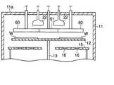
このCVD成膜装置10は、真空引き可能に構成された略円筒状のチャンバー11を有しており、その中には被処理体であるウエハWを水平に4枚支持可能なウエハ支持部材12が設けられている。ウエハ支持部材12は、図2に示すように、4つのウエハ支持部12aを有しており、これらにウエハWが支持されるようになっている。また、ウエハ支持部材12の中心には下方に延びる回転軸13が設けられており、この回転軸13はモーター14の軸に取り付けられている。そして、このモーター14を回転させることにより、回転軸13を介してウエハ支持部材12が図2の矢印方向に沿って回転されるようになっている。したがって、ウエハ支持部12aに支持されたウエハWは、ウエハ支持部材12の回転によって回転軸13の回りを公転するようになっている。
【0022】
ウエハ支持部材12の下方には、ヒーター支持部材15が設けられており、このヒーター支持部材15には、ウエハWの移動軌跡に沿って内側および外側2つの円環状のヒーター16が支持されている。
【0023】
チャンバー11の天壁11aには、第1の処理ガス吐出ノズル(第1の処理ガス吐出部)20および第2の処理ガス吐出ノズル(第2の処理ガス吐出部)21が、そのガス吐出口20a,20bをウエハ支持部材12の上面に対向させた状態で設けられている。これら第1の処理ガス吐出ノズル20および第2の処理ガス吐出ノズル21は、図2に示すように2つずつ、中心側から外周側に向けて放射状に設けられており、これらは交互にウエハWの移動軌跡に沿って円周状に配置されている。これら第1の処理ガス吐出ノズル20および第2の処理ガス吐出ノズル21は、チャンバー11の径方向に長く、チャンバー11の周方向に短い扁平状をなしており、径方向の長さが支持部材12に支持されたウエハWの直径よりも長くなるように設けられている。また、隣接する第1の処理ガス吐出ノズル20および第2の処理ガス吐出ノズル21は回転軸13を中心として90°の角度で配置されている。また、チャンバー11の天壁11aには、4つのパージガス吐出ノズル(パージガス吐出部)22が隣接する第1の処理ガス吐出ノズル20および第2の処理ガス吐出ノズル21の間に位置するように設けられている。これら4つのパージガス吐出ノズル22はそれぞれ独立した状態で中心側から外周側に向けて放射状に設けられており、チャンバー11の径方向に長く、チャンバー11の周方向に短い扁平状をなしている。また、パージガス吐出ノズル22は、径方向の長さが支持部材12に支持されたウエハWの直径よりも長くなるように設けられている。
【0024】
図3(a)は第1の処理ガス吐出ノズル20および第2の処理ガス吐出ノズル21の断面図である。図3(a)に示すように、第1および第2の処理ガス吐出ノズル20,21は、それぞれ多数のガス吐出口20a,21aを有しており、この多数の吐出口20a,21aからチャンバー11内にシャワー状に処理ガスを吐出するように構成されている。また、図3(b)はパージガス吐出ノズル22の断面図である。図3(b)に示すように、パージガス吐出ノズル22の内部には多数の吐出口22aが設けられている。この多数の吐出口22aからは、ウエハ支持部材12に向けて直接ガスが吐出される。また、このパージガス吐出ノズル22は、多数の吐出口22aの下方に延びるように設けられたスカート部22bを有しており、吐出口22aからチャンバー11内にシャワー状にパージガスを吐出するとともに、スカート部22bによりシャワー状に吐出されたパージガスの流れが拡散することを防止しており、これによりパージガスのダウンフローがエアカーテンをなすように構成されている。そして、上述したように、パージガス吐出ノズル22は放射状に設けられ、その径方向の長さがウエハ支持部材12上のウエハWの長さよりも長いので、多数の吐出口22aも放射状にかつ支持部材12上のウエハWの長さよりも長い長さで分布し、吐出口22aから吐出されたパージガスのエアカーテンをウエハ支持部材12が通過する際に、その上のウエハWの全面がもれなくパージガスのエアカーテンを通過するようになる。すなわち、支持部材12上のウエハWを基準にすると、そのウエハW上をパージガスのエアカーテンが漏れなく走査可能となっている。このようなパージガスのエアカーテンにより、2つの処理ガスの分離性を高めることができる。
【0025】
また、パージガス吐出ノズル22のガス吐出口22aは、第1の処理ガス吐出ノズル20および第2の処理ガス吐出ノズル21のガス吐出口20a,21aよりも上方に設けられており、これにより第1の処理ガス雰囲気と第2の処理ガス雰囲気とをパージガスのエアカーテンにより分離可能になっている。これらノズル20,21,22からは、後述するガス供給機構30から所定のガスが供給されるようになっている。
【0026】
ガス供給機構30は、クリーニングガスであるClF3を供給するClF3供給源31、Arを供給するAr供給源32、TiCl4を供給するTiCl4供給源33、NH3を供給するNH3供給源34を有している。そして、ClF3供給源31にはClF3ガスライン35が、Ar供給源32にはArガスライン36が、TiCl4供給源33にはTiCl4ガスライン37が、NH3供給源34にはNH3ガスライン38がそれぞれ接続されている。そして、各ラインにはバルブ40およびマスフローコントローラ41が設けられている。
【0027】
TiCl4供給源33から延びるTiCl4ガスライン37は、第1の処理ガス吐出ノズル20から延びるガス配管42に接続されている。また、TiCl4ガスライン37にはArガスライン36から延びる配管45が接続されており、ArガスにキャリアされたTiCl4ガスが配管42を通って第1の処理ガス吐出ノズル20から吐出される。また、NH3供給源34から延びるNH3ガスライン38は、第2の処理ガス吐出ノズル21から延びるガス配管43に接続されており、NH3ガスがNH3ガスライン38およびガス配管43を通って第2の処理ガス吐出ノズル21から吐出される。さらに、Ar供給源32から延びるArガスライン36は、パージガス吐出ノズル22から延びる配管44に接続されており、ArガスがArガスライン36および配管44を通ってパージガス吐出ノズル22から吐出される。さらにまた、ClF3供給源31から延びるClF3ガスライン35には、配管46,47,48が接続されており、これら配管46,47,48から配管42,43,44を介して第1の処理ガス吐出ノズル20、第2の処理ガス吐出ノズル21、およびパージガス吐出ノズル22からクリーニングガスであるClF3ガスを吐出可能となっている。なお、配管45,46,47,48には、それぞれバルブ45a,46a,47a,48aが設けられている。
【0028】
チャンバー11の底壁11bには、その中央部に排気口25が設けられており、この排気口25には排気管26が接続されている。この排気管26には排気装置28が接続されており、排気装置28を作動させることによりチャンバー11内を所定の真空度まで減圧することができる。
【0029】
なお、排気管26は排気口25から垂直方向下方に延び途中で水平方向に屈曲しており、前記回転軸13は排気管26の垂直部の中を通って、排気管26の水平部の管壁を貫通して下方へ延びており、その管壁と回転軸13との間には、流体シール27が設けられている。
【0030】
このように構成されたCVD成膜装置においては、まず、チャンバー11内に半導体ウエハWを装入し、ウエハ支持部材12のウエハ支持部12aにウエハWを載置する。次いで、ヒーター16よりウエハWを加熱しながらウエハ支持部材12を回転させ、排気装置28によりチャンバー11内を排気してチャンバー11内を所定の真空状態にする。引き続き、第1の処理ガス吐出ノズル20からArにキャリアさせたTiCl4ガスを、第2の処理ガス吐出ノズル21からNH3ガスを、パージガス吐出ノズル22からパージガスとしてのArガスをそれぞれ吐出させる。
【0031】
ウエハ支持部材12のウエハ支持部12aのウエハWのうち、最初に第1の処理ガス吐出ノズル20から吐出されたTiCl4ガスが供給される2枚については、供給されたTiCl4ガスによりTiの単原子層が吸着した後、ウエハ支持部材12の回転により、パージガス吐出ノズル22から吐出されたArガスのエアカーテンを通過して、第2の処理ガス吐出ノズル21から吐出されたNH3ガスによりTiの単原子層の上にNの単原子層が堆積され、これらが反応してTiNが形成される。さらに、パージガス吐出ノズル22から吐出されたArガスのエアカーテンを通過した後、同様にしてTiの単原子層およびNの単原子層が供給され、これが所定回数繰り返されて所定厚さのTiN膜が形成される。また、最初に第2の処理ガス吐出ノズル21から吐出されたNH3ガスが供給される他の2枚については、供給されたNH3ガスによりNの単原子層が吸着した後、ウエハ支持部材12の回転により、パージガス吐出ノズル22から吐出されたArガスのエアカーテンを通過して、第1の処理ガス吐出ノズル20から吐出されたTiCl4ガスによりNの単原子層の上にTiの単原子層が堆積され、これらが反応してTiNが形成される。さらに、パージガス吐出ノズル22から吐出されたArガスのエアカーテンを通過した後、同様にしてNの単原子層およびTiの単原子層が供給され、これが所定回数繰り返されて所定厚さのTiN膜が形成される。この場合に、ウエハ支持部材12の回転速度は、処理ガスであるTiCl4ガスおよびNH3ガスの吸着速度に応じて決定される。
【0032】
また、この場合における第1の処理ガス吐出ノズル20および第2の処理ガス吐出ノズル21の形状およびウエハWとの間隔、さらにはガス流量は、ウエハWに均等に単原子層が吸着するような流れを形成することができるように設定される。また、パージガス吐出ノズル22とウエハWとの間隔、さらにはガス流量は、パージガスがTiCl4ガス雰囲気およびNH3ガス雰囲気を十分に分離可能なエアカーテンとして機能する流れを形成することができるように設定される。また、ヒーター16の加熱温度はTiとNとの反応に適した適宜の温度に設定される。以下、これらの設定値について具体的に述べる。
【0033】
図3(a)に示した構造を有する第1の処理ガス吐出ノズル20および第2の処理ガス吐出ノズル21は、吐出口20a,21aとその下方に位置する基板支持部材12に保持されたウエハW表面との間の距離h1が0.1〜10mmとなるように配置することができる。また、図3(b)に示した構造を有するパージガス吐出ノズル22は、吐出口22aとその下方に位置する基板支持部材12に保持されたウエハW表面との間の距離h2が0.1〜50mmとなるように配置することができ、その下端と基板支持部材12上面との間の距離h3が1.1〜50mmとなるように配置することができる。好ましくは、h1が0.1〜5mm、h2が0.2〜10mm、h3が1.2〜11mmとなるようにノズル20,21,22を配置する。
【0034】
また、TiN成膜時におけるそれぞれのガス流量、チャンバー内圧力および加熱温度は、以下のように設定することができる。
TiCl4ガス流量:1〜50sccm(0.001〜0.05L/min)、好ましくは5〜20sccm(0.005〜0.02L/min)
Arガス(キャリアガス)流量:10〜100sccm(0.01〜0.1L/min)、TiCl4ガスが低流量の場合にはキャリアガスは用いなくてもよい
NH3ガス流量:50〜1000sccm(0.05〜1L/min)、好ましくは50〜500sccm(0.05〜0.5L/min)
パージガス流量:100〜1000sccm(0.1〜1L/min)
チャンバー内圧力:100mTorr〜5Torr(13.3Pa〜665Pa)、好ましくは100mTorr〜1Torr(13.3Pa〜133Pa)
加熱温度:300〜700℃、好ましくは400〜600℃
【0035】
以上のようにして、交互に配置された第1の処理ガス吐出ノズル20および第2の処理ガス吐出ノズル21からそれぞれTiCl4ガスおよびNH3ガスを供給しつつ、ウエハ支持部材12を回転させて、ウエハWにTiCl4ガスおよびNH3ガスを交互に供給するので、高速スイッチングバルブを用いることなく、ALD法によりTiの単原子層およびNの単原子層を交互に形成して所望のTiN膜を形成することができる。また、このようにウエハ支持部材12に複数枚のウエハWを載置し、一回の処理で複数枚の成膜処理を行うから、生産性が高い。また、パージガス吐出ノズル22からパージガスとしてのArガスを吐出してエアカーテンを形成することにより、TiCl4ガスおよびNH3ガスが混合することを極力防止することができ、また、パージガスであるArガスを吐出することにより、ウエハWの単原子層の形成が終了した部分の処理ガスを速やかに除去して余分な反応を防止することができるので、より良質の膜を形成することができる。
【0036】
このようなTiN膜の形成を繰り返し行い、所定枚数のウエハWの成膜処理が終了した時点で、ClF3源31からガスライン35、配管46,47,48および配管42,43,44を介してノズル20,21,22からClF3ガスを吐出させてチャンバー11内をクリーニングする。
【0037】
このクリーニング時におけるClF3ガス流量、チャンバー内圧力、クリーニング温度は、例えば以下に示すように設定することができる。
ClF3ガス流量:100〜500sccm(0.1〜0.5L/min)、好ましくは200〜300sccm(0.2〜0.3L/min)
チャンバー内圧力:1〜10Torr(133〜1330Pa)、好ましくは1〜5Torr(133〜665Pa)
クリーニング温度:200〜500℃、好ましくは200〜300℃
【0038】
次に、他の実施形態に係るCVD成膜装置について説明する。図4は他の実施形態に係るCVD成膜装置を部分的に示す断面図である。ここでは、ウエハ支持部材12の代わりにウエハ支持部材12’を用いてウエハWを自転させる構成となっている。すなわち、ウエハ支持部材12’は、ベース部材51の上に、4つ(図4では2つのみ図示)のウエハテーブル52が回転可能に設けられ、これらウエハテーブル52をモーター53により回転させることにより、ウエハテーブル52上のウエハWを自転させる。これにより、処理ガスとしてのTiCl4ガスおよびNH3ガスをより一層均一にウエハWに供給することができ、より均一な単原子層を形成することができる。この場合に、図1のようにヒーター16がウエハ支持部材の下にあると、加熱効率が悪くなるため、図4のようにウエハWの上方にヒーター16’を設けることが好ましい。15’はヒーター16’を支持するヒーター支持部材である。このようにヒーターを設けた場合には、処理ガスがウエハWに有効に供給されるようにヒーター16’およびヒーター支持部材15’にガス通過可能な多数の孔を設けることが好ましい。
【0039】
さらに、図5の実施形態では、処理ガスとしてのTiCl4ガスおよびNH3ガスをそれぞれシャワーヘッド60およびシャワーヘッド61から供給するようにしている。シャワーヘッド60は、図6に示すように、ディスク状をなす中空の本体60aの下面に多数のガス吐出孔60bが形成されており、このガス吐出孔60bから均一にガスを吐出する。シャワーヘッド61も同様に構成されている。このようにノズルの代わりにシャワーヘッドを用いることによってもウエハWに均一にTiCl4ガスおよびNH3ガスを供給することができる。
【0040】
さらにまた、図7の実施形態では、第1の処理ガス吐出ノズル20および第2の処理ガス吐出ノズル21の直下に排気口70を設けている(第1の処理ガス吐出ノズル20に対応する排気口のみ図示)。このようにすることにより、不要なTiCl4ガスおよびNH3ガスを排気口70に接続された排気管71を介して速やかに排出することができる。
【0041】
なお、本発明は、上記実施の形態に限定されることなく種々変形可能である。例えば、上記実施形態では、TiN膜を成膜する例について示したが、Al2O3、ZrO2、TaN、SiO2、SiN、SiON、WN、WSi、RuO2等、他の金属化合物も同様にして成膜することができる。また、上記実施形態では、第1の処理ガスとしてTiCl4を用い、第2の処理ガスとしてNH3ガスを用いたが、第1の処理ガスと第2の処理ガスとは成膜する金属化合物膜に応じた適宜のガスを用いることができる。このような場合における第1の処理ガスとしては、TiCl4の他に、TaBr5、Ta(OC2H5)5、SiCl4、SiH4、Si2H6、SiH2Cl2、WF6等のAl、Zr、Ti、Ta、Si、WおよびRuのうち1種を含むものを挙げることができ、第2の処理ガスとしては、NH3の他に、NH3(N2)、O2、O3、NO、N2O、N2O3、N2O5等のNまたはOを含むものを挙げることができる。
【0042】
また、ヒーターの位置を図1の例ではウエハの下方に、図4の例ではウエハの上方に設けたが、これら両方に設けてもよいし、均一に加熱することができれば他の位置に設けてもよい。さらに、パージガスとしてArガスを用いたが、N2ガス等他のガスであってもよい。また、2つの処理ガスを有効に遮断することができれば、パージガスを用いなくてもよい。さらにまた、用いる基板としては、半導体ウエハに限らず他のものであってもよく、また、表面上に他の層を形成した基板であってもよい。
【0043】
【発明の効果】
以上説明したように、本発明によれば、ALD法を利用した成膜を行うにあたり、互いに異なる位置に設けられた第1の処理ガス吐出部および第2の処理ガスを吐出する第2の処理ガス吐出部からそれぞれ第1の処理ガスおよび第2の処理ガスを吐出し、基板支持部材を回転させるので、高速スイッチングバルブを用いることなく、基板上に第1の処理ガスと第2の処理ガスとを交互に供給して吸着させ、第1の処理ガスによる単原子層と、第2の処理ガスによる単原子層とを交互に形成することができる。また、基板支持部材に複数の基板を支持した状態で処理を行うので、一度に複数枚数の基板の成膜処理を行うことができ、生産性を高めることができる。
【図面の簡単な説明】
【図1】本発明の一実施形態に係るCVD成膜装置を示す断面図。
【図2】図1のCVD成膜装置の内部を示す平面図。
【図3】図1のCVD成膜装置における第1の処理ガス吐出ノズルおよびパージガス吐出ノズルの断面図。
【図4】本発明の他の実施形態に係るCVD成膜装置を部分的に示す断面図。
【図5】本発明のさらに他の実施形態に係るCVD成膜装置を部分的に示す断面図。
【図6】図4の装置に用いたシャワーヘッドを示す斜視図。
【図7】本発明のさらに他の実施形態に係るCVD成膜装置を部分的に示す断面図。
【符号の説明】
11;チャンバー
12,12’;ウエハ支持部材
12a;ウエハ支持部
13;回転軸
14;モーター
16,16’;ヒーター
20,21;処理ガス吐出ノズル
22;パージガス吐出ノズル
30;ガス供給機構
25,70;排気口
26,71;排気管
28;排気装置
52;ウエハテーブル
53;モーター
60,61;シャワーヘッド
W;半導体ウエハ[0001]
BACKGROUND OF THE INVENTION
The present invention relates to a film forming apparatus and a film forming method for forming a TiN film or the like using an ALD (Atomic Layer Deposition) method.
[0002]
[Prior art]
In a semiconductor manufacturing process, WSi (tungsten silicide), TiN (titanium nitride) are used as a barrier layer for embedding holes between wirings formed in a semiconductor wafer (hereinafter simply referred to as a wafer) as an object to be processed. ), A metal compound such as TiSi (titanium silicide) is deposited to form a thin film.
[0003]
Conventionally, these metal compound thin films have been formed using physical vapor deposition (PVD), but recently, miniaturization and high integration of devices are particularly required, and design rules have become particularly strict, It is difficult to obtain sufficient characteristics with PVD having poor properties. Therefore, a TiN film is formed by chemical vapor deposition (CVD) that can be expected to form a higher quality film.
[0004]
However, even with CVD, film quality, step coverage, and film adhesion are not necessarily sufficient. Further, it is very difficult to control the film thickness when forming an ultrathin film of 10 nm or less.
[0005]
On the other hand, the ALD method has recently attracted attention as a technique for forming a metal compound thin film with good film quality with good adhesion and step coverage (Japanese Patent Laid-Open No. 55-130896, etc.). Therefore, it is conceivable to use the ALD method also in the deposition of the metal compound. Specifically, for example, when forming a TiN film, a single wafer is placed in the chamber, and TiCl is first placed in the chamber.4A gas is supplied to adsorb the Ti monolayer and then NH3A gas is supplied to deposit a monolayer of N thereon and react them. By repeating this operation a predetermined number of times, a TiN film having a predetermined thickness is obtained.
[0006]
[Problems to be solved by the invention]
However, when forming a metal compound thin film using the ALD method, the supplied gas must be switched at a high speed. For this reason, a high-speed switching valve is used. There is a problem that it is short. In addition, when laminating monoatomic layers in this way, it is necessary to purge the previous gas by supplying a purge gas while supplying one gas and then supplying the other gas. There is also the problem that it takes time and productivity is poor.
[0007]
The present invention has been made in view of such circumstances, and an object thereof is to provide a film forming apparatus and a film forming method that can use the ALD method without using a high-speed switching valve and with high productivity. To do.
[0008]
In order to solve the above problems, the present invention includes a chamber for accommodating a substrate,
A substrate support member for planarly supporting a plurality of substrates in the chamber;
The substrate support member provided in the chamberAboveA first processing gas discharge section having a plurality of discharge ports for discharging the first processing gas in a state of being opposed to each other;
Provided in a position different from the first processing gas discharge section in the chamber,substrateSupport memberAboveA second processing gas discharge section having a plurality of discharge ports for discharging the second processing gas in a state of being opposed to each other;
A purge gas discharge section for discharging a purge gas, disposed in a state of being opposed to the upper side of the substrate support member between the first process gas discharge section and the second process gas discharge section;
A rotation mechanism for rotating the substrate support member;
Heating means for heating the substrate;
An exhaust port provided at the bottom of the chamber;
Comprising
The first process gas discharge part and the second process gas discharge part are alternately arranged in a circle around the rotation axis of the rotation mechanism,
The purge gas discharge portion has a plurality of discharge ports therein, and extends downward from the plurality of discharge ports, and has a skirt portion that prevents the purge gas flow from being diffused. The purge gas becomes an air curtain by the skirt portion, and the atmosphere of the first processing gas and the atmosphere of the second processing gas are separated by the air curtain,
The rotation mechanism rotates the substrate support member so that the substrate supported by the substrate support member passes immediately below the first process gas discharge unit and the second process gas discharge unit,
By rotating the substrate support member by the rotation mechanism, the substrate support member was separated by a purge gas from the first process gas discharge unit and the second process gas discharge unit above the substrate toward the exhaust port at the bottom. Passing the substrate heated by the heating means through the first process gas flow and the second process gas flow in a state;On the substrate, the first processing gas and the second processing gas,Without mixing with each otherAlternately adsorbing to form a monoatomic layer of the first process gas and a monoatomic layer of the second process gas, and reacting them thermally to form a compound film. A characteristic film forming apparatus is provided.
[0009]
The present invention also provides:A chamber for housing the substrate;
A substrate support member for planarly supporting a plurality of substrates in the chamber;
A first processing gas discharge unit provided in the chamber and having a plurality of discharge ports for discharging the first processing gas in a state of being opposed to the upper side of the substrate support member;
A second process is provided in the chamber at a position different from the first process gas discharge part, and has a plurality of discharge ports for discharging a second process gas in a state of being opposed to the upper side of the substrate support member. A gas discharge part;
A purge gas discharge section for discharging a purge gas, disposed in a state of being opposed to the upper side of the substrate support member between the first process gas discharge section and the second process gas discharge section;
A rotation mechanism for rotating the substrate support member;
Heating means for heating the substrate;
An exhaust port provided at the bottom of the chamber;
Comprising
The first process gas discharge part and the second process gas discharge part are alternately arranged in a circle around the rotation axis of the rotation mechanism,
The purge gas discharge portion has a plurality of discharge ports therein, and has a skirt portion that extends downward from the plurality of discharge ports and prevents the purge gas flow from diffusing,
The rotation mechanism is a film forming apparatus that rotates the substrate support member so that the substrate supported by the substrate support member passes immediately below the first process gas discharge unit and the second process gas discharge unit. A film forming method for forming a compound film on a substrate using a method,
The purge gas discharged from the purge gas discharge part is used as an air curtain by the skirt part, and the atmosphere of the first process gas and the atmosphere of the second process gas are separated by the air curtain, and the atmosphere above the substrate is A flow of the first process gas and the second process gas separated from each other by a purge gas is formed from the first process gas discharge unit and the second process gas discharge unit toward the exhaust port at the bottom. And
By rotating the substrate support member by the rotation mechanism, the substrate heated by the heating means is passed through the flow of the first processing gas and the second processing gas,
The first processing gas and the second processing gas are alternately adsorbed on the heated substrate without being mixed with each other, so that the monoatomic layer and the second processing by the first processing gas are used. A method of forming a film comprising alternately forming monoatomic layers of gas and thermally reacting them to form a compound filmI will provide a.
[0011]
According to the present invention, when the film formation is performed using the ALD method, the first process gas discharge section and the first process gas discharge section provided at different positions are provided.SecondThe first processing gas and the second processing gas are discharged from the two processing gas discharge portions,In the meantime, an air curtain-like purge gas is discharged to separate the first processing gas and the second processing gas, and in the flow of the first processing gas and the second processing gas separated by the purge gas. In addition, the substrate heated by the heating means is passed by rotating the substrate support member by the rotation mechanism.So without using a high speed switching valveIn a state where the first processing gas and the second processing gas are reliably separatedA first processing gas and a second processing gas are alternately supplied and adsorbed on the substrate to alternately form a monoatomic layer of the first processing gas and a monoatomic layer of the second processing gas. be able to. Also,The first process gas discharge part and the second process gas discharge part are alternately arranged in a circle around the rotation axis of the rotation mechanism, andSince the processing is performed in a state where a plurality of substrates are supported on the substrate support member, a plurality of substrates can be formed at a time, and productivity can be improved.
[0012]
In the film forming apparatus, it is preferable that the first process gas discharge unit and the second process gas discharge unit have a large number of discharge ports so that the process gas is discharged in a shower shape.Yes.
[0013]
in frontThe purge gas discharge section is arranged so that a distance between the discharge port for discharging the purge gas and the substrate held by the substrate holding member located below is 0.1 to 50 mm. preferable. Moreover, it is preferable that the said purge gas discharge part is arrange | positioned so that the distance between the lower end and the said board | substrate holding member upper surface may be 1.1-50 mm. Further, the height position of the discharge port of the purge gas discharge portion is higher than the height position of the discharge port in the first processing gas discharge portion and the height position of the discharge port in the second processing gas discharge portion. Is preferred. By providing the purge gas discharge portion in this way, the separation between the first processing gas and the second processing gas is improved.ThanCan be increased.
[0014]
in frontThe rotation speed of the rotation mechanism is preferably variable according to the adsorption speed of the first process gas and the second process gas.
[0015]
It is preferable to further have a substrate rotation mechanism for rotating the substrate. By rotating the substrate in this manner, the uniformity of film formation can be further improved.
[0016]
It is preferable that the heating unit includes a heater supported by a heater support member that is separated from the substrate support member below the substrate support member.further,The heater isSaidsubstrateAlong the movement trajectory of the substrate as the support member rotatesCircleRingFormed inIt is preferable.
[0017]
In the film forming method, it is preferable to further rotate the substrate. Also, according to the adsorption speed of the first and second processing gasesThe substrate support memberIs preferably rotated.
[0018]
The first processing gas may include any one of Al, Zr, Ti, Ta, Si, W, and Ru, and the second processing gas may include N or O. Can be used.
[0019]
The film forming apparatus and the film forming method are made of Al.2O3, ZrO2TiN, TaN, SiO2, SiN, SiON, SiOF, WN, WSi and RuO2It can apply to any 1 type of film-forming.Further, the first process gas discharge unit and the second process gas discharge unit can discharge the cleaning gas to clean the inside of the chamber. In this case, ClF is used as the cleaning gas.3Can be used.
[0020]
DETAILED DESCRIPTION OF THE INVENTION
Embodiments of the present invention will be described below in detail with reference to the accompanying drawings. FIG. 1 is a sectional view showing a film forming apparatus according to an embodiment of the present invention, and FIG. 2 is a plan view of the inside thereof. Here, a case where a TiN film is formed by a CVD film forming apparatus using the ALD method will be described.
[0021]
The CVD
[0022]
A
[0023]
A first process gas discharge nozzle (first process gas discharge unit) 20 and a second process gas discharge nozzle (second process gas discharge unit) 21 are provided on the
[0024]
FIG. 3A is a cross-sectional view of the first process
[0025]
Further, the
[0026]
The
[0027]
TiCl4TiCl extending from
[0028]
The
[0029]
The
[0030]
In the CVD film forming apparatus configured as described above, first, the semiconductor wafer W is loaded into the
[0031]
Of the wafer W of the
[0032]
In this case, the shape of the first process
[0033]
The first processing
[0034]
Further, each gas flow rate, chamber internal pressure, and heating temperature during TiN film formation can be set as follows.
TiCl4Gas flow rate: 1-50 sccm (0.001-0.05 L / min), preferably 5-20 sccm (0.005-0.02 L / min)
Ar gas (carrier gas) flow rate: 10 to 100 sccm (0.01 to 0.1 L / min), TiCl4Carrier gas may not be used when the gas has a low flow rate.
NH3Gas flow rate: 50 to 1000 sccm (0.05 to 1 L / min), preferably 50 to 500 sccm (0.05 to 0.5 L / min)
Purge gas flow rate: 100 to 1000 sccm (0.1 to 1 L / min)
Pressure in chamber: 100 mTorr to 5 Torr (13.3 Pa to 665 Pa), preferably 100 mTorr to 1 Torr (13.3 Pa to 133 Pa)
Heating temperature: 300-700 ° C, preferably 400-600 ° C
[0035]
As described above, each of the first processing
[0036]
When such a TiN film is repeatedly formed and a predetermined number of wafers W have been formed, ClF3ClF from the
[0037]
ClF during this cleaning3The gas flow rate, the pressure in the chamber, and the cleaning temperature can be set as shown below, for example.
ClF3Gas flow rate: 100 to 500 sccm (0.1 to 0.5 L / min), preferably 200 to 300 sccm (0.2 to 0.3 L / min)
Pressure in chamber: 1 to 10 Torr (133 to 1330 Pa), preferably 1 to 5 Torr (133 to 665 Pa)
Cleaning temperature: 200-500 ° C, preferably 200-300 ° C
[0038]
Next, a CVD film forming apparatus according to another embodiment will be described. FIG. 4 is a sectional view partially showing a CVD film forming apparatus according to another embodiment. Here, the wafer W is rotated using a
[0039]
Further, in the embodiment of FIG. 5, TiCl as a processing gas is used.4Gas and NH3Gas is supplied from the
[0040]
Furthermore, in the embodiment of FIG. 7, an
[0041]
The present invention can be variously modified without being limited to the above embodiment. For example, in the above embodiment, an example in which a TiN film is formed has been described.2O3, ZrO2, TaN, SiO2, SiN, SiON, WN, WSi, RuO2Other metal compounds can be formed in the same manner. In the above embodiment, TiCl is used as the first processing gas.4And NH as the second process gas3Although the gas is used, the first processing gas and the second processing gas can be any gas suitable for the metal compound film to be formed. The first process gas in such a case is TiCl.4Besides, TaBr5, Ta (OC2H5)5, SiCl4, SiH4, Si2H6, SiH2Cl2, WF6Examples of the second processing gas include NH, Zr, Ti, Ta, Si, W, and Ru.3Besides, NH3(N2), O2, O3, NO, N2O, N2O3, N2O5And the like containing N or O.
[0042]
Further, although the heater is provided below the wafer in the example of FIG. 1 and above the wafer in the example of FIG. 4, it may be provided on both of them, or provided at other positions if uniform heating is possible. May be. Furthermore, Ar gas was used as the purge gas, but N2Other gases such as gas may be used. In addition, the purge gas may not be used as long as the two processing gases can be effectively shut off. Furthermore, the substrate to be used is not limited to a semiconductor wafer, and may be a substrate in which another layer is formed on the surface.
[0043]
【The invention's effect】
As described above, according to the present invention, when performing film formation using the ALD method, the first process gas discharge unit and the second process gas that discharge the second process gas provided at different positions are used. The first processing gas and the second processing gas are discharged from the gas discharge unit, respectively, and the substrate support member is rotated.MakeSo without using a fast switching valveThe first processing gas and the second processing gas are alternately supplied onto the substrate to be adsorbed.A monoatomic layer made of the first processing gas and a monoatomic layer made of the second processing gas can be alternately formed. In addition, since the processing is performed in a state where a plurality of substrates are supported on the substrate support member, a plurality of substrates can be formed at a time, and productivity can be improved.
[Brief description of the drawings]
FIG. 1 is a cross-sectional view showing a CVD film forming apparatus according to an embodiment of the present invention.
FIG. 2 is a plan view showing the inside of the CVD film forming apparatus of FIG.
3 is a cross-sectional view of a first process gas discharge nozzle and a purge gas discharge nozzle in the CVD film forming apparatus of FIG. 1. FIG.
FIG. 4 is a cross-sectional view partially showing a CVD film forming apparatus according to another embodiment of the present invention.
FIG. 5 is a cross-sectional view partially showing a CVD film forming apparatus according to still another embodiment of the present invention.
6 is a perspective view showing a shower head used in the apparatus of FIG. 4;
FIG. 7 is a sectional view partially showing a CVD film forming apparatus according to still another embodiment of the present invention.
[Explanation of symbols]
11; chamber
12, 12 '; Wafer support member
12a: Wafer support
13: Rotating shaft
14; Motor
16, 16 '; heater
20, 21; processing gas discharge nozzle
22: Purge gas discharge nozzle
30; Gas supply mechanism
25, 70; exhaust port
26, 71; exhaust pipe
28; exhaust system
52; Wafer table
53; Motor
60, 61; shower head
W: Semiconductor wafer
Claims (20)
Translated fromJapanese前記チャンバー内で複数の基板を平面的に支持する基板支持部材と、
前記チャンバー内に設けられ、前記基板支持部材の上方に対向させた状態で第1の処理ガスを吐出する複数の吐出口を有する第1の処理ガス吐出部と、
前記チャンバー内の前記第1の処理ガス吐出部とは異なる位置に設けられ、前記基板支持部材の上方に対向させた状態で第2の処理ガスを吐出する複数の吐出口を有する第2の処理ガス吐出部と、
前記第1の処理ガス吐出部と前記第2の処理ガス吐出部との間に前記基板支持部材の上方に対向させた状態で配置された、パージガスを吐出するパージガス吐出部と、
前記基板支持部材を回転させる回転機構と、
前記基板を加熱する加熱手段と、
前記チャンバーの底部に設けられた排気口と
を具備し、
前記第1の処理ガス吐出部と前記第2の処理ガス吐出部とは、前記回転機構の回転軸を中心として、円周状に交互に配置されており、
前記パージガス吐出部は、その内部に多数の吐出口を有し、かつ前記多数の吐出口よりも下方に延び、前記パージガスの流れが拡散することを防止するスカート部を有し、吐出された前記パージガスが前記スカート部によってエアカーテンとなり、このエアカーテンにより前記第1の処理ガスの雰囲気と前記第2の処理ガスの雰囲気とが分離され、
前記回転機構は、前記基板支持部材に支持された基板が前記第1の処理ガス吐出部および前記第2の処理ガス吐出部の直下を通過するように前記基板支持部材を回転させ、
前記回転機構により前記基板支持部材を回転させることにより、基板の上方の前記第1の処理ガス吐出部および前記第2の処理ガス吐出部から底部の前記排気口に向けた、パージガスで分離された状態の前記第1の処理ガスの流れおよび前記第2の処理ガスの流れの中に前記加熱手段により加熱された状態の基板を通過させ、基板上に、前記第1の処理ガスおよび前記第2の処理ガスを、互いに混合することなく交互に吸着させて、前記第1の処理ガスによる単原子層および前記第2の処理ガスによる単原子層とを交互に形成し、これらを熱的に反応させて化合物の膜を形成することを特徴とする成膜装置。A chamber for housing the substrate;
A substrate support member for planarly supporting a plurality of substrates in the chamber;
A first processing gas discharge unit provided in the chamber and having a plurality of discharge ports for discharging the first processing gas in a state ofbeing opposed tothe upper side of the substrate support member;
A second process is provided in the chamber at a position different from the first process gas discharge part, and has a plurality of discharge ports for discharging a second process gas in a state ofbeing opposed tothe upper side of thesubstrate support member. A gas discharge part;
A purge gas discharge section for discharging a purge gas, disposed in a state of being opposed to the upper side of the substrate support member between the first process gas discharge section and the second process gas discharge section;
A rotation mechanism for rotating the substrate support member;
Heating means for heating the substrate;
An exhaust port provided at the bottom of the chamber;
The first process gas discharge part and the second process gas discharge part are alternately arranged in a circle around the rotation axis of the rotation mechanism,
The purge gas discharge portion has a plurality of discharge ports therein, and extends downward from the plurality of discharge ports, and has a skirt portion that prevents the purge gas flow from being diffused. The purge gas becomes an air curtain by the skirt portion, and the atmosphere of the first processing gas and the atmosphere of the second processing gas are separated by the air curtain,
The rotation mechanism rotates the substrate support member so that the substrate supported by the substrate support member passes immediately below the first process gas discharge unit and the second process gas discharge unit,
By rotating the substrate support member by the rotation mechanism, the substrate support member was separated by a purge gas from the first process gas discharge unit and the second process gas discharge unit above the substrate toward the exhaust port at the bottom. A substrate heated by the heating means is passed through the first process gas flow and the second process gas flow in a state, and the first process gas and the second process gasare passed over the substrate. The process gas is alternately adsorbedwithout beingmixed with each other, so that a monoatomic layer of the first process gas and a monoatomic layer of the second process gas are alternately formed, and these are reacted thermally. And forming a film of the compound.
前記チャンバー内で複数の基板を平面的に支持する基板支持部材と、 A substrate support member for planarly supporting a plurality of substrates in the chamber;
前記チャンバー内に設けられ、前記基板支持部材の上方に対向させた状態で第1の処理ガスを吐出する複数の吐出口を有する第1の処理ガス吐出部と、 A first processing gas discharge unit provided in the chamber and having a plurality of discharge ports for discharging the first processing gas in a state of being opposed to the upper side of the substrate support member;
前記チャンバー内の前記第1の処理ガス吐出部とは異なる位置に設けられ、前記基板支持部材の上方に対向させた状態で第2の処理ガスを吐出する複数の吐出口を有する第2の処理ガス吐出部と、 A second process is provided in the chamber at a position different from the first process gas discharge part, and has a plurality of discharge ports for discharging a second process gas in a state of being opposed to the upper side of the substrate support member. A gas discharge part;
前記第1の処理ガス吐出部と前記第2の処理ガス吐出部との間に前記基板支持部材の上方に対向させた状態で配置された、パージガスを吐出するパージガス吐出部と、 A purge gas discharge section for discharging a purge gas, disposed in a state of being opposed to the upper side of the substrate support member between the first process gas discharge section and the second process gas discharge section;
前記基板支持部材を回転させる回転機構と、 A rotation mechanism for rotating the substrate support member;
前記基板を加熱する加熱手段と、 Heating means for heating the substrate;
前記チャンバーの底部に設けられた排気口と An exhaust port provided at the bottom of the chamber;
を具備し、Comprising
前記第1の処理ガス吐出部と前記第2の処理ガス吐出部とは、前記回転機構の回転軸を中心として、円周状に交互に配置されており、 The first process gas discharge part and the second process gas discharge part are alternately arranged in a circle around the rotation axis of the rotation mechanism,
前記パージガス吐出部は、その内部に多数の吐出口を有し、かつ前記多数の吐出口よりも下方に延び、前記パージガスの流れが拡散することを防止するスカート部を有し、 The purge gas discharge portion has a plurality of discharge ports therein, and has a skirt portion that extends downward from the plurality of discharge ports and prevents the purge gas flow from diffusing,
前記回転機構は、前記基板支持部材に支持された基板が前記第1の処理ガス吐出部および前記第2の処理ガス吐出部の直下を通過するように前記基板支持部材を回転させる成膜装置を用いて基板上に化合物膜を成膜する成膜方法であって、 The rotation mechanism is a film forming apparatus that rotates the substrate support member so that the substrate supported by the substrate support member passes immediately below the first process gas discharge unit and the second process gas discharge unit. A film forming method for forming a compound film on a substrate using a method,
前記パージガス吐出部から吐出された前記パージガスを前記スカート部によってエアカーテンとし、このエアカーテンにより前記第1の処理ガスの雰囲気と前記第2の処理ガスの雰囲気とを分離し、基板の上方の前記第1の処理ガス吐出部および前記第2の処理ガス吐出部から底部の前記排気口に向けた、パージガスで分離された状態の前記第1の処理ガスおよび前記第2の処理ガスの流れを形成し、 The purge gas discharged from the purge gas discharge part is used as an air curtain by the skirt part, and the atmosphere of the first process gas and the atmosphere of the second process gas are separated by the air curtain, and the atmosphere above the substrate is A flow of the first process gas and the second process gas separated from each other by a purge gas is formed from the first process gas discharge unit and the second process gas discharge unit toward the exhaust port at the bottom. And
前記回転機構により前記基板支持部材を回転させることにより、前記第1の処理ガスおよび前記第2の処理ガスの流れの中に前記加熱手段により加熱された状態の基板を通過させ、 By rotating the substrate support member by the rotation mechanism, the substrate heated by the heating means is passed through the flow of the first processing gas and the second processing gas,
前記加熱された基板上に、前記第1の処理ガスおよび前記第2の処理ガスを、互いに混合することなく交互に吸着させて、前記第1の処理ガスによる単原子層および前記第2の処理ガスによる単原子層とを交互に形成し、これらを熱的に反応させて化合物の膜を形成することを特徴とする成膜方法。 The first processing gas and the second processing gas are alternately adsorbed on the heated substrate without being mixed with each other, so that the monoatomic layer and the second processing by the first processing gas are used. A film forming method comprising alternately forming monoatomic layers of gas and thermally reacting them to form a compound film.
Priority Applications (1)
| Application Number | Priority Date | Filing Date | Title |
|---|---|---|---|
| JP2001000183AJP4817210B2 (en) | 2000-01-06 | 2001-01-04 | Film forming apparatus and film forming method |
Applications Claiming Priority (4)
| Application Number | Priority Date | Filing Date | Title |
|---|---|---|---|
| JP2000000590 | 2000-01-06 | ||
| JP2000000590 | 2000-01-06 | ||
| JP2000-590 | 2000-01-06 | ||
| JP2001000183AJP4817210B2 (en) | 2000-01-06 | 2001-01-04 | Film forming apparatus and film forming method |
Related Child Applications (4)
| Application Number | Title | Priority Date | Filing Date |
|---|---|---|---|
| JP2008089537ADivisionJP4817268B2 (en) | 2000-01-06 | 2008-03-31 | Film forming apparatus and film forming method |
| JP2008089536ADivisionJP4817267B2 (en) | 2000-01-06 | 2008-03-31 | Film forming apparatus and film forming method |
| JP2008089538ADivisionJP2008208462A (en) | 2000-01-06 | 2008-03-31 | Film depositing apparatus and film depositing method |
| JP2008089535ADivisionJP4817266B2 (en) | 2000-01-06 | 2008-03-31 | Film forming apparatus and film forming method |
Publications (3)
| Publication Number | Publication Date |
|---|---|
| JP2001254181A JP2001254181A (en) | 2001-09-18 |
| JP2001254181A5 JP2001254181A5 (en) | 2011-04-07 |
| JP4817210B2true JP4817210B2 (en) | 2011-11-16 |
Family
ID=26583182
Family Applications (1)
| Application Number | Title | Priority Date | Filing Date |
|---|---|---|---|
| JP2001000183AExpired - Fee RelatedJP4817210B2 (en) | 2000-01-06 | 2001-01-04 | Film forming apparatus and film forming method |
Country Status (1)
| Country | Link |
|---|---|
| JP (1) | JP4817210B2 (en) |
Cited By (2)
| Publication number | Priority date | Publication date | Assignee | Title |
|---|---|---|---|---|
| US10072336B2 (en) | 2014-10-31 | 2018-09-11 | Tokyo Electron Limited | Film forming apparatus, film forming method, and recording medium |
| US10683573B2 (en) | 2014-11-13 | 2020-06-16 | Tokyo Electron Limited | Film forming apparatus |
Families Citing this family (147)
| Publication number | Priority date | Publication date | Assignee | Title |
|---|---|---|---|---|
| KR100385946B1 (en)* | 1999-12-08 | 2003-06-02 | 삼성전자주식회사 | Method for forming a metal layer by an atomic layer deposition and a semiconductor device with the metal layer as a barrier metal layer, an upper electrode, or a lower electrode of capacitor |
| US6974766B1 (en) | 1998-10-01 | 2005-12-13 | Applied Materials, Inc. | In situ deposition of a low κ dielectric layer, barrier layer, etch stop, and anti-reflective coating for damascene application |
| US6620723B1 (en) | 2000-06-27 | 2003-09-16 | Applied Materials, Inc. | Formation of boride barrier layers using chemisorption techniques |
| US7101795B1 (en) | 2000-06-28 | 2006-09-05 | Applied Materials, Inc. | Method and apparatus for depositing refractory metal layers employing sequential deposition techniques to form a nucleation layer |
| US6551929B1 (en) | 2000-06-28 | 2003-04-22 | Applied Materials, Inc. | Bifurcated deposition process for depositing refractory metal layers employing atomic layer deposition and chemical vapor deposition techniques |
| US6936538B2 (en) | 2001-07-16 | 2005-08-30 | Applied Materials, Inc. | Method and apparatus for depositing tungsten after surface treatment to improve film characteristics |
| US7732327B2 (en) | 2000-06-28 | 2010-06-08 | Applied Materials, Inc. | Vapor deposition of tungsten materials |
| US7405158B2 (en) | 2000-06-28 | 2008-07-29 | Applied Materials, Inc. | Methods for depositing tungsten layers employing atomic layer deposition techniques |
| US7964505B2 (en) | 2005-01-19 | 2011-06-21 | Applied Materials, Inc. | Atomic layer deposition of tungsten materials |
| US6825447B2 (en) | 2000-12-29 | 2004-11-30 | Applied Materials, Inc. | Apparatus and method for uniform substrate heating and contaminate collection |
| US6765178B2 (en) | 2000-12-29 | 2004-07-20 | Applied Materials, Inc. | Chamber for uniform substrate heating |
| US6998579B2 (en) | 2000-12-29 | 2006-02-14 | Applied Materials, Inc. | Chamber for uniform substrate heating |
| JP4590744B2 (en)* | 2001-01-25 | 2010-12-01 | ソニー株式会社 | Nonvolatile semiconductor memory device and manufacturing method thereof |
| US6951804B2 (en) | 2001-02-02 | 2005-10-04 | Applied Materials, Inc. | Formation of a tantalum-nitride layer |
| US6660126B2 (en) | 2001-03-02 | 2003-12-09 | Applied Materials, Inc. | Lid assembly for a processing system to facilitate sequential deposition techniques |
| US6878206B2 (en) | 2001-07-16 | 2005-04-12 | Applied Materials, Inc. | Lid assembly for a processing system to facilitate sequential deposition techniques |
| US6734020B2 (en) | 2001-03-07 | 2004-05-11 | Applied Materials, Inc. | Valve control system for atomic layer deposition chamber |
| US6596643B2 (en) | 2001-05-07 | 2003-07-22 | Applied Materials, Inc. | CVD TiSiN barrier for copper integration |
| US7211144B2 (en) | 2001-07-13 | 2007-05-01 | Applied Materials, Inc. | Pulsed nucleation deposition of tungsten layers |
| US9051641B2 (en) | 2001-07-25 | 2015-06-09 | Applied Materials, Inc. | Cobalt deposition on barrier surfaces |
| US20090004850A1 (en) | 2001-07-25 | 2009-01-01 | Seshadri Ganguli | Process for forming cobalt and cobalt silicide materials in tungsten contact applications |
| US8110489B2 (en) | 2001-07-25 | 2012-02-07 | Applied Materials, Inc. | Process for forming cobalt-containing materials |
| US20030029715A1 (en) | 2001-07-25 | 2003-02-13 | Applied Materials, Inc. | An Apparatus For Annealing Substrates In Physical Vapor Deposition Systems |
| JP2005504885A (en) | 2001-07-25 | 2005-02-17 | アプライド マテリアルズ インコーポレイテッド | Barrier formation using a novel sputter deposition method |
| US7085616B2 (en) | 2001-07-27 | 2006-08-01 | Applied Materials, Inc. | Atomic layer deposition apparatus |
| US6936906B2 (en) | 2001-09-26 | 2005-08-30 | Applied Materials, Inc. | Integration of barrier layer and seed layer |
| CN102361004B (en)* | 2001-09-26 | 2016-02-10 | 应用材料公司 | Barrier layer and seed layer integrated |
| US7049226B2 (en) | 2001-09-26 | 2006-05-23 | Applied Materials, Inc. | Integration of ALD tantalum nitride for copper metallization |
| US6916398B2 (en) | 2001-10-26 | 2005-07-12 | Applied Materials, Inc. | Gas delivery apparatus and method for atomic layer deposition |
| US7780785B2 (en) | 2001-10-26 | 2010-08-24 | Applied Materials, Inc. | Gas delivery apparatus for atomic layer deposition |
| US7081271B2 (en) | 2001-12-07 | 2006-07-25 | Applied Materials, Inc. | Cyclical deposition of refractory metal silicon nitride |
| US6729824B2 (en) | 2001-12-14 | 2004-05-04 | Applied Materials, Inc. | Dual robot processing system |
| US6620670B2 (en) | 2002-01-18 | 2003-09-16 | Applied Materials, Inc. | Process conditions and precursors for atomic layer deposition (ALD) of AL2O3 |
| US6998014B2 (en) | 2002-01-26 | 2006-02-14 | Applied Materials, Inc. | Apparatus and method for plasma assisted deposition |
| US6911391B2 (en) | 2002-01-26 | 2005-06-28 | Applied Materials, Inc. | Integration of titanium and titanium nitride layers |
| US6827978B2 (en) | 2002-02-11 | 2004-12-07 | Applied Materials, Inc. | Deposition of tungsten films |
| US6833161B2 (en) | 2002-02-26 | 2004-12-21 | Applied Materials, Inc. | Cyclical deposition of tungsten nitride for metal oxide gate electrode |
| JP4361921B2 (en)* | 2002-03-26 | 2009-11-11 | 東京エレクトロン株式会社 | Substrate processing equipment |
| US7439191B2 (en) | 2002-04-05 | 2008-10-21 | Applied Materials, Inc. | Deposition of silicon layers for active matrix liquid crystal display (AMLCD) applications |
| US7279432B2 (en) | 2002-04-16 | 2007-10-09 | Applied Materials, Inc. | System and method for forming an integrated barrier layer |
| JP4158139B2 (en)* | 2002-04-30 | 2008-10-01 | スズキ株式会社 | Thin film manufacturing method and apparatus |
| KR100498609B1 (en)* | 2002-05-18 | 2005-07-01 | 주식회사 하이닉스반도체 | Batch type atomic layer deposition equipment |
| US6838114B2 (en) | 2002-05-24 | 2005-01-04 | Micron Technology, Inc. | Methods for controlling gas pulsing in processes for depositing materials onto micro-device workpieces |
| US7041335B2 (en) | 2002-06-04 | 2006-05-09 | Applied Materials, Inc. | Titanium tantalum nitride silicide layer |
| US6821347B2 (en) | 2002-07-08 | 2004-11-23 | Micron Technology, Inc. | Apparatus and method for depositing materials onto microelectronic workpieces |
| US6838125B2 (en) | 2002-07-10 | 2005-01-04 | Applied Materials, Inc. | Method of film deposition using activated precursor gases |
| US20040014327A1 (en)* | 2002-07-18 | 2004-01-22 | Bing Ji | Method for etching high dielectric constant materials and for cleaning deposition chambers for high dielectric constant materials |
| KR100476370B1 (en)* | 2002-07-19 | 2005-03-16 | 주식회사 하이닉스반도체 | Batch type Atomic Layer Deposition and method for insitu-cleaning in the batch type atomic layer deposition |
| TW200411923A (en)* | 2002-07-19 | 2004-07-01 | Asml Us Inc | In-situ formation of metal insulator metal capacitors |
| US6955725B2 (en) | 2002-08-15 | 2005-10-18 | Micron Technology, Inc. | Reactors with isolated gas connectors and methods for depositing materials onto micro-device workpieces |
| US6821563B2 (en) | 2002-10-02 | 2004-11-23 | Applied Materials, Inc. | Gas distribution system for cyclical layer deposition |
| JP4113755B2 (en)* | 2002-10-03 | 2008-07-09 | 東京エレクトロン株式会社 | Processing equipment |
| US7244683B2 (en) | 2003-01-07 | 2007-07-17 | Applied Materials, Inc. | Integration of ALD/CVD barriers with porous low k materials |
| US7262133B2 (en) | 2003-01-07 | 2007-08-28 | Applied Materials, Inc. | Enhancement of copper line reliability using thin ALD tan film to cap the copper line |
| JP3973567B2 (en)* | 2003-01-17 | 2007-09-12 | 東京エレクトロン株式会社 | Thin film forming method and thin film forming apparatus |
| JP4257576B2 (en) | 2003-03-25 | 2009-04-22 | ローム株式会社 | Deposition equipment |
| US7211508B2 (en) | 2003-06-18 | 2007-05-01 | Applied Materials, Inc. | Atomic layer deposition of tantalum based barrier materials |
| KR101070353B1 (en)* | 2003-06-25 | 2011-10-05 | 주성엔지니어링(주) | Gas injector for use in semiconductor fabrication apparatus |
| US7344755B2 (en) | 2003-08-21 | 2008-03-18 | Micron Technology, Inc. | Methods and apparatus for processing microfeature workpieces; methods for conditioning ALD reaction chambers |
| US7235138B2 (en) | 2003-08-21 | 2007-06-26 | Micron Technology, Inc. | Microfeature workpiece processing apparatus and methods for batch deposition of materials on microfeature workpieces |
| US7422635B2 (en) | 2003-08-28 | 2008-09-09 | Micron Technology, Inc. | Methods and apparatus for processing microfeature workpieces, e.g., for depositing materials on microfeature workpieces |
| JP2005089781A (en)* | 2003-09-12 | 2005-04-07 | Mitsui Eng & Shipbuild Co Ltd | Thin film forming equipment |
| US7056806B2 (en) | 2003-09-17 | 2006-06-06 | Micron Technology, Inc. | Microfeature workpiece processing apparatus and methods for controlling deposition of materials on microfeature workpieces |
| US7282239B2 (en) | 2003-09-18 | 2007-10-16 | Micron Technology, Inc. | Systems and methods for depositing material onto microfeature workpieces in reaction chambers |
| US7323231B2 (en) | 2003-10-09 | 2008-01-29 | Micron Technology, Inc. | Apparatus and methods for plasma vapor deposition processes |
| US7581511B2 (en) | 2003-10-10 | 2009-09-01 | Micron Technology, Inc. | Apparatus and methods for manufacturing microfeatures on workpieces using plasma vapor processes |
| US7647886B2 (en) | 2003-10-15 | 2010-01-19 | Micron Technology, Inc. | Systems for depositing material onto workpieces in reaction chambers and methods for removing byproducts from reaction chambers |
| US7258892B2 (en) | 2003-12-10 | 2007-08-21 | Micron Technology, Inc. | Methods and systems for controlling temperature during microfeature workpiece processing, e.g., CVD deposition |
| US7906393B2 (en) | 2004-01-28 | 2011-03-15 | Micron Technology, Inc. | Methods for forming small-scale capacitor structures |
| US7584942B2 (en) | 2004-03-31 | 2009-09-08 | Micron Technology, Inc. | Ampoules for producing a reaction gas and systems for depositing materials onto microfeature workpieces in reaction chambers |
| KR101178743B1 (en)* | 2004-04-12 | 2012-09-07 | 가부시키가이샤 알박 | Method for forming barrier film, and method for forming electrode film |
| US8133554B2 (en) | 2004-05-06 | 2012-03-13 | Micron Technology, Inc. | Methods for depositing material onto microfeature workpieces in reaction chambers and systems for depositing materials onto microfeature workpieces |
| US20050252449A1 (en) | 2004-05-12 | 2005-11-17 | Nguyen Son T | Control of gas flow and delivery to suppress the formation of particles in an MOCVD/ALD system |
| US8323754B2 (en) | 2004-05-21 | 2012-12-04 | Applied Materials, Inc. | Stabilization of high-k dielectric materials |
| US7699932B2 (en) | 2004-06-02 | 2010-04-20 | Micron Technology, Inc. | Reactors, systems and methods for depositing thin films onto microfeature workpieces |
| JP2006028577A (en)* | 2004-07-15 | 2006-02-02 | Canon Anelva Corp | CVD equipment |
| JP4515227B2 (en)* | 2004-11-15 | 2010-07-28 | 古河機械金属株式会社 | Vapor growth equipment |
| US7429402B2 (en) | 2004-12-10 | 2008-09-30 | Applied Materials, Inc. | Ruthenium as an underlayer for tungsten film deposition |
| JP2007112677A (en)* | 2005-10-21 | 2007-05-10 | Takao Kamiyama | Continuous manufacturing apparatus of nano carbon and its continuous manufacture method |
| TWI332532B (en) | 2005-11-04 | 2010-11-01 | Applied Materials Inc | Apparatus and process for plasma-enhanced atomic layer deposition |
| DE102005055468A1 (en)* | 2005-11-22 | 2007-05-24 | Aixtron Ag | Coating one or more substrates comprises supplying gases to process chamber via chambers with gas outlet openings |
| US20070234956A1 (en)* | 2006-04-05 | 2007-10-11 | Dalton Jeremie J | Method and apparatus for providing uniform gas delivery to a reactor |
| US7798096B2 (en) | 2006-05-05 | 2010-09-21 | Applied Materials, Inc. | Plasma, UV and ion/neutral assisted ALD or CVD in a batch tool |
| KR100794657B1 (en) | 2006-06-28 | 2008-01-14 | 삼성전자주식회사 | Method of forming barrier metal film in semiconductor device |
| RU2331717C2 (en)* | 2006-10-02 | 2008-08-20 | Общество с ограниченной ответственностью "Наноинженерия"(ООО "Наноинженерия") | Device for thin film coating of semi-conductors and dielectrics |
| US7521379B2 (en) | 2006-10-09 | 2009-04-21 | Applied Materials, Inc. | Deposition and densification process for titanium nitride barrier layers |
| US8043432B2 (en)* | 2007-02-12 | 2011-10-25 | Tokyo Electron Limited | Atomic layer deposition systems and methods |
| US8465592B2 (en) | 2008-08-25 | 2013-06-18 | Tokyo Electron Limited | Film deposition apparatus |
| US8465591B2 (en) | 2008-06-27 | 2013-06-18 | Tokyo Electron Limited | Film deposition apparatus |
| JP5310283B2 (en)* | 2008-06-27 | 2013-10-09 | 東京エレクトロン株式会社 | Film forming method, film forming apparatus, substrate processing apparatus, and storage medium |
| US8808456B2 (en) | 2008-08-29 | 2014-08-19 | Tokyo Electron Limited | Film deposition apparatus and substrate process apparatus |
| US9416448B2 (en) | 2008-08-29 | 2016-08-16 | Tokyo Electron Limited | Film deposition apparatus, substrate processing apparatus, film deposition method, and computer-readable storage medium for film deposition method |
| JP5195175B2 (en) | 2008-08-29 | 2013-05-08 | 東京エレクトロン株式会社 | Film forming apparatus, film forming method, and storage medium |
| JP5423205B2 (en) | 2008-08-29 | 2014-02-19 | 東京エレクトロン株式会社 | Deposition equipment |
| JP5253933B2 (en) | 2008-09-04 | 2013-07-31 | 東京エレクトロン株式会社 | Film forming apparatus, substrate processing apparatus, film forming method, and storage medium |
| JP5107185B2 (en) | 2008-09-04 | 2012-12-26 | 東京エレクトロン株式会社 | Film forming apparatus, substrate processing apparatus, film forming method, and recording medium recording program for executing this film forming method |
| JP5276387B2 (en)* | 2008-09-04 | 2013-08-28 | 東京エレクトロン株式会社 | Film forming apparatus, substrate processing apparatus, film forming method, and recording medium recording program for executing this film forming method |
| JP5276388B2 (en) | 2008-09-04 | 2013-08-28 | 東京エレクトロン株式会社 | Film forming apparatus and substrate processing apparatus |
| US8961691B2 (en) | 2008-09-04 | 2015-02-24 | Tokyo Electron Limited | Film deposition apparatus, film deposition method, computer readable storage medium for storing a program causing the apparatus to perform the method |
| JP5253932B2 (en) | 2008-09-04 | 2013-07-31 | 東京エレクトロン株式会社 | Film forming apparatus, substrate processing apparatus, film forming method, and storage medium |
| US20100062149A1 (en) | 2008-09-08 | 2010-03-11 | Applied Materials, Inc. | Method for tuning a deposition rate during an atomic layer deposition process |
| US8491967B2 (en) | 2008-09-08 | 2013-07-23 | Applied Materials, Inc. | In-situ chamber treatment and deposition process |
| JP5544697B2 (en)* | 2008-09-30 | 2014-07-09 | 東京エレクトロン株式会社 | Deposition equipment |
| JP5445044B2 (en)* | 2008-11-14 | 2014-03-19 | 東京エレクトロン株式会社 | Deposition equipment |
| JP5031013B2 (en)* | 2008-11-19 | 2012-09-19 | 東京エレクトロン株式会社 | Film forming apparatus, film forming apparatus cleaning method, program, and computer-readable storage medium storing program |
| US9297072B2 (en) | 2008-12-01 | 2016-03-29 | Tokyo Electron Limited | Film deposition apparatus |
| JP5056735B2 (en) | 2008-12-02 | 2012-10-24 | 東京エレクトロン株式会社 | Deposition equipment |
| JP5068780B2 (en)* | 2009-03-04 | 2012-11-07 | 東京エレクトロン株式会社 | Film forming apparatus, film forming method, program, and computer-readable storage medium |
| JP5093162B2 (en)* | 2009-03-12 | 2012-12-05 | 東京エレクトロン株式会社 | Film forming apparatus, film forming method, and storage medium |
| US20100227059A1 (en)* | 2009-03-04 | 2010-09-09 | Tokyo Electron Limited | Film deposition apparatus, film deposition method, and computer readable storage medium |
| JP5141607B2 (en)* | 2009-03-13 | 2013-02-13 | 東京エレクトロン株式会社 | Deposition equipment |
| JP5131240B2 (en) | 2009-04-09 | 2013-01-30 | 東京エレクトロン株式会社 | Film forming apparatus, film forming method, and storage medium |
| JP5181100B2 (en) | 2009-04-09 | 2013-04-10 | 東京エレクトロン株式会社 | Substrate processing apparatus, substrate processing method, and storage medium |
| KR101108879B1 (en)* | 2009-08-31 | 2012-01-30 | 주식회사 원익아이피에스 | Gas injection device and substrate processing device using the same |
| KR101625078B1 (en)* | 2009-09-02 | 2016-05-27 | 주식회사 원익아이피에스 | Gas injecting device and Substrate processing apparatus using the same |
| JP5434484B2 (en) | 2009-11-02 | 2014-03-05 | 東京エレクトロン株式会社 | Film forming apparatus, film forming method, and storage medium |
| JP5553588B2 (en)* | 2009-12-10 | 2014-07-16 | 東京エレクトロン株式会社 | Deposition equipment |
| US8034723B2 (en) | 2009-12-25 | 2011-10-11 | Tokyo Electron Limited | Film deposition apparatus and film deposition method |
| JP5392069B2 (en)* | 2009-12-25 | 2014-01-22 | 東京エレクトロン株式会社 | Deposition equipment |
| JP5396264B2 (en)* | 2009-12-25 | 2014-01-22 | 東京エレクトロン株式会社 | Deposition equipment |
| JP5482196B2 (en)* | 2009-12-25 | 2014-04-23 | 東京エレクトロン株式会社 | Film forming apparatus, film forming method, and storage medium |
| KR101205433B1 (en) | 2010-07-28 | 2012-11-28 | 국제엘렉트릭코리아 주식회사 | Substrate susceptor and depositon apparatus using sysceptor |
| JP5602711B2 (en) | 2011-05-18 | 2014-10-08 | 東京エレクトロン株式会社 | Film forming method and film forming apparatus |
| JP5696619B2 (en)* | 2011-08-17 | 2015-04-08 | 東京エレクトロン株式会社 | Deposition equipment |
| US20130196078A1 (en)* | 2012-01-31 | 2013-08-01 | Joseph Yudovsky | Multi-Chamber Substrate Processing System |
| US20130192761A1 (en)* | 2012-01-31 | 2013-08-01 | Joseph Yudovsky | Rotary Substrate Processing System |
| KR20130106906A (en)* | 2012-03-21 | 2013-10-01 | 주식회사 윈텔 | Substrate processing apparatus and substrate processing method |
| JP5403113B2 (en)* | 2012-06-15 | 2014-01-29 | 東京エレクトロン株式会社 | Deposition equipment |
| JP5953994B2 (en)* | 2012-07-06 | 2016-07-20 | 東京エレクトロン株式会社 | Film forming apparatus and film forming method |
| JP6262115B2 (en) | 2014-02-10 | 2018-01-17 | 東京エレクトロン株式会社 | Substrate processing method and substrate processing apparatus |
| JP5800952B1 (en)* | 2014-04-24 | 2015-10-28 | 株式会社日立国際電気 | Substrate processing apparatus, semiconductor device manufacturing method, program, and recording medium |
| JP5764246B1 (en)* | 2014-09-24 | 2015-08-19 | 株式会社日立国際電気 | Substrate processing apparatus, gas introduction shaft and gas supply plate |
| JP6441050B2 (en)* | 2014-12-01 | 2018-12-19 | 東京エレクトロン株式会社 | Deposition method |
| JP6557992B2 (en)* | 2015-02-25 | 2019-08-14 | 東京エレクトロン株式会社 | Film forming apparatus, film forming method, and storage medium |
| CN107835868B (en)* | 2015-06-17 | 2020-04-10 | 应用材料公司 | Gas control in a processing chamber |
| JP6507953B2 (en)* | 2015-09-08 | 2019-05-08 | 東京エレクトロン株式会社 | Substrate processing apparatus and substrate processing method |
| JP6548586B2 (en) | 2016-02-03 | 2019-07-24 | 東京エレクトロン株式会社 | Deposition method |
| JP6697067B2 (en)* | 2016-02-23 | 2020-05-20 | 株式会社Kokusai Electric | Substrate processing apparatus, semiconductor device manufacturing method, and computer-readable recording medium |
| JP6708167B2 (en)* | 2016-08-03 | 2020-06-10 | 東京エレクトロン株式会社 | Film forming apparatus, film forming method and storage medium |
| KR101861008B1 (en) | 2016-08-26 | 2018-05-25 | 한양대학교 산학협력단 | Atomic Layer Deposition Apparatus and Deposition Method Using the Same |
| JP6767844B2 (en) | 2016-11-11 | 2020-10-14 | 東京エレクトロン株式会社 | Film formation equipment and film formation method |
| JP6733516B2 (en) | 2016-11-21 | 2020-08-05 | 東京エレクトロン株式会社 | Method of manufacturing semiconductor device |
| US11574826B2 (en)* | 2019-07-12 | 2023-02-07 | Applied Materials, Inc. | High-density substrate processing systems and methods |
| US20210013069A1 (en)* | 2019-07-12 | 2021-01-14 | Applied Materials, Inc. | Multi-lid structure for semiconductor processing system |
| JP7325313B2 (en)* | 2019-12-11 | 2023-08-14 | 東京エレクトロン株式会社 | Rotation drive device, substrate processing device, and rotation drive method |
| KR20230065384A (en)* | 2020-05-20 | 2023-05-11 | 램 리써치 코포레이션 | Remote-plasma clean (rpc) directional-flow device |
| KR102793771B1 (en)* | 2024-07-22 | 2025-04-11 | 주식회사 피앤에스인터내셔날 | Work table changing structure for semiconductor grinding apparatus |
Family Cites Families (5)
| Publication number | Priority date | Publication date | Assignee | Title |
|---|---|---|---|---|
| JPS6226811A (en)* | 1985-07-26 | 1987-02-04 | Fujitsu Ltd | Semiconductor manufacturing equipment |
| JPH04287912A (en)* | 1991-02-19 | 1992-10-13 | Mitsubishi Electric Corp | Semiconductor manufacturing device |
| JPH05251701A (en)* | 1992-03-04 | 1993-09-28 | Fujitsu Ltd | Method of forming thin film transistor |
| JP2963973B2 (en)* | 1993-09-17 | 1999-10-18 | 東京エレクトロン株式会社 | Batch type cold wall processing apparatus and cleaning method thereof |
| JP4114972B2 (en)* | 1997-05-27 | 2008-07-09 | キヤノンアネルバ株式会社 | Substrate processing equipment |
- 2001
- 2001-01-04JPJP2001000183Apatent/JP4817210B2/ennot_activeExpired - Fee Related
Cited By (3)
| Publication number | Priority date | Publication date | Assignee | Title |
|---|---|---|---|---|
| US10072336B2 (en) | 2014-10-31 | 2018-09-11 | Tokyo Electron Limited | Film forming apparatus, film forming method, and recording medium |
| US11085113B2 (en) | 2014-10-31 | 2021-08-10 | Tokyo Electron Limited | Film forming method and recording medium |
| US10683573B2 (en) | 2014-11-13 | 2020-06-16 | Tokyo Electron Limited | Film forming apparatus |
Also Published As
| Publication number | Publication date |
|---|---|
| JP2001254181A (en) | 2001-09-18 |
Similar Documents
| Publication | Publication Date | Title |
|---|---|---|
| JP4817210B2 (en) | Film forming apparatus and film forming method | |
| JP4817267B2 (en) | Film forming apparatus and film forming method | |
| JP6690496B2 (en) | Film forming method and film forming apparatus | |
| US7763115B2 (en) | Vacuum film-forming apparatus | |
| JP5482196B2 (en) | Film forming apparatus, film forming method, and storage medium | |
| JP4288767B2 (en) | Manufacturing method of semiconductor device | |
| CN102134709B (en) | Film deposition apparatus | |
| JPWO2006041169A1 (en) | Substrate processing apparatus and semiconductor device manufacturing method | |
| TWI390076B (en) | Method for depositing thin film and thin film deposition system having separate jet orifices for spraying purge gas | |
| JP2021125610A (en) | Film formation method and film forming device | |
| KR101862907B1 (en) | Film forming method | |
| US11710633B2 (en) | Deposition method and deposition apparatus | |
| KR101485506B1 (en) | Method for depositing thin film on wafer | |
| JP6971887B2 (en) | Film formation method and film formation equipment | |
| JP6910118B2 (en) | Film formation method and film formation system, and surface treatment method | |
| JP2004277772A (en) | Treatment device | |
| JP6544232B2 (en) | Film forming method and film forming apparatus | |
| CN112391612B (en) | Film forming method and film forming apparatus | |
| KR100422398B1 (en) | Apparatus for depositing a thin film | |
| JP7243521B2 (en) | Film forming method and film forming apparatus | |
| JP7279605B2 (en) | Deposition apparatus and operation method of the deposition apparatus | |
| TWI576461B (en) | Thin film deposition method | |
| JP2004217956A (en) | Substrate processing equipment |
Legal Events
| Date | Code | Title | Description |
|---|---|---|---|
| A521 | Written amendment | Free format text:JAPANESE INTERMEDIATE CODE: A523 Effective date:20071228 | |
| A621 | Written request for application examination | Free format text:JAPANESE INTERMEDIATE CODE: A621 Effective date:20071228 | |
| A521 | Written amendment | Free format text:JAPANESE INTERMEDIATE CODE: A523 Effective date:20080501 | |
| A521 | Written amendment | Free format text:JAPANESE INTERMEDIATE CODE: A821 Effective date:20080501 | |
| A977 | Report on retrieval | Free format text:JAPANESE INTERMEDIATE CODE: A971007 Effective date:20100412 | |
| A521 | Written amendment | Free format text:JAPANESE INTERMEDIATE CODE: A523 Effective date:20101210 | |
| A131 | Notification of reasons for refusal | Free format text:JAPANESE INTERMEDIATE CODE: A131 Effective date:20110531 | |
| A521 | Written amendment | Free format text:JAPANESE INTERMEDIATE CODE: A523 Effective date:20110721 | |
| TRDD | Decision of grant or rejection written | ||
| A01 | Written decision to grant a patent or to grant a registration (utility model) | Free format text:JAPANESE INTERMEDIATE CODE: A01 Effective date:20110824 | |
| A01 | Written decision to grant a patent or to grant a registration (utility model) | Free format text:JAPANESE INTERMEDIATE CODE: A01 | |
| A61 | First payment of annual fees (during grant procedure) | Free format text:JAPANESE INTERMEDIATE CODE: A61 Effective date:20110824 | |
| FPAY | Renewal fee payment (event date is renewal date of database) | Free format text:PAYMENT UNTIL: 20140909 Year of fee payment:3 | |
| R150 | Certificate of patent or registration of utility model | Free format text:JAPANESE INTERMEDIATE CODE: R150 Ref document number:4817210 Country of ref document:JP Free format text:JAPANESE INTERMEDIATE CODE: R150 | |
| R250 | Receipt of annual fees | Free format text:JAPANESE INTERMEDIATE CODE: R250 | |
| R250 | Receipt of annual fees | Free format text:JAPANESE INTERMEDIATE CODE: R250 | |
| LAPS | Cancellation because of no payment of annual fees |