JP4816668B2 - Display device with touch sensor - Google Patents
Display device with touch sensorDownload PDFInfo
- Publication number
- JP4816668B2 JP4816668B2JP2008087739AJP2008087739AJP4816668B2JP 4816668 B2JP4816668 B2JP 4816668B2JP 2008087739 AJP2008087739 AJP 2008087739AJP 2008087739 AJP2008087739 AJP 2008087739AJP 4816668 B2JP4816668 B2JP 4816668B2
- Authority
- JP
- Japan
- Prior art keywords
- electrode
- display
- touch
- common electrode
- touch sensor
- Prior art date
- Legal status (The legal status is an assumption and is not a legal conclusion. Google has not performed a legal analysis and makes no representation as to the accuracy of the status listed.)
- Active
Links
Images


Classifications
- G—PHYSICS
- G02—OPTICS
- G02F—OPTICAL DEVICES OR ARRANGEMENTS FOR THE CONTROL OF LIGHT BY MODIFICATION OF THE OPTICAL PROPERTIES OF THE MEDIA OF THE ELEMENTS INVOLVED THEREIN; NON-LINEAR OPTICS; FREQUENCY-CHANGING OF LIGHT; OPTICAL LOGIC ELEMENTS; OPTICAL ANALOGUE/DIGITAL CONVERTERS
- G02F1/00—Devices or arrangements for the control of the intensity, colour, phase, polarisation or direction of light arriving from an independent light source, e.g. switching, gating or modulating; Non-linear optics
- G02F1/01—Devices or arrangements for the control of the intensity, colour, phase, polarisation or direction of light arriving from an independent light source, e.g. switching, gating or modulating; Non-linear optics for the control of the intensity, phase, polarisation or colour
- G02F1/13—Devices or arrangements for the control of the intensity, colour, phase, polarisation or direction of light arriving from an independent light source, e.g. switching, gating or modulating; Non-linear optics for the control of the intensity, phase, polarisation or colour based on liquid crystals, e.g. single liquid crystal display cells
- G02F1/133—Constructional arrangements; Operation of liquid crystal cells; Circuit arrangements
- G02F1/1333—Constructional arrangements; Manufacturing methods
- G02F1/13338—Input devices, e.g. touch panels
- G—PHYSICS
- G06—COMPUTING OR CALCULATING; COUNTING
- G06F—ELECTRIC DIGITAL DATA PROCESSING
- G06F3/00—Input arrangements for transferring data to be processed into a form capable of being handled by the computer; Output arrangements for transferring data from processing unit to output unit, e.g. interface arrangements
- G06F3/01—Input arrangements or combined input and output arrangements for interaction between user and computer
- G06F3/03—Arrangements for converting the position or the displacement of a member into a coded form
- G06F3/041—Digitisers, e.g. for touch screens or touch pads, characterised by the transducing means
- G06F3/0412—Digitisers structurally integrated in a display
- G—PHYSICS
- G02—OPTICS
- G02F—OPTICAL DEVICES OR ARRANGEMENTS FOR THE CONTROL OF LIGHT BY MODIFICATION OF THE OPTICAL PROPERTIES OF THE MEDIA OF THE ELEMENTS INVOLVED THEREIN; NON-LINEAR OPTICS; FREQUENCY-CHANGING OF LIGHT; OPTICAL LOGIC ELEMENTS; OPTICAL ANALOGUE/DIGITAL CONVERTERS
- G02F1/00—Devices or arrangements for the control of the intensity, colour, phase, polarisation or direction of light arriving from an independent light source, e.g. switching, gating or modulating; Non-linear optics
- G02F1/01—Devices or arrangements for the control of the intensity, colour, phase, polarisation or direction of light arriving from an independent light source, e.g. switching, gating or modulating; Non-linear optics for the control of the intensity, phase, polarisation or colour
- G02F1/13—Devices or arrangements for the control of the intensity, colour, phase, polarisation or direction of light arriving from an independent light source, e.g. switching, gating or modulating; Non-linear optics for the control of the intensity, phase, polarisation or colour based on liquid crystals, e.g. single liquid crystal display cells
- G02F1/133—Constructional arrangements; Operation of liquid crystal cells; Circuit arrangements
- G02F1/1333—Constructional arrangements; Manufacturing methods
- G02F1/1343—Electrodes
- G02F1/134309—Electrodes characterised by their geometrical arrangement
- G02F1/134363—Electrodes characterised by their geometrical arrangement for applying an electric field parallel to the substrate, i.e. in-plane switching [IPS]
- G—PHYSICS
- G06—COMPUTING OR CALCULATING; COUNTING
- G06F—ELECTRIC DIGITAL DATA PROCESSING
- G06F3/00—Input arrangements for transferring data to be processed into a form capable of being handled by the computer; Output arrangements for transferring data from processing unit to output unit, e.g. interface arrangements
- G06F3/01—Input arrangements or combined input and output arrangements for interaction between user and computer
- G06F3/03—Arrangements for converting the position or the displacement of a member into a coded form
- G06F3/041—Digitisers, e.g. for touch screens or touch pads, characterised by the transducing means
- G06F3/044—Digitisers, e.g. for touch screens or touch pads, characterised by the transducing means by capacitive means
- G06F3/0443—Digitisers, e.g. for touch screens or touch pads, characterised by the transducing means by capacitive means using a single layer of sensing electrodes
- G—PHYSICS
- G06—COMPUTING OR CALCULATING; COUNTING
- G06F—ELECTRIC DIGITAL DATA PROCESSING
- G06F3/00—Input arrangements for transferring data to be processed into a form capable of being handled by the computer; Output arrangements for transferring data from processing unit to output unit, e.g. interface arrangements
- G06F3/01—Input arrangements or combined input and output arrangements for interaction between user and computer
- G06F3/03—Arrangements for converting the position or the displacement of a member into a coded form
- G06F3/041—Digitisers, e.g. for touch screens or touch pads, characterised by the transducing means
- G06F3/044—Digitisers, e.g. for touch screens or touch pads, characterised by the transducing means by capacitive means
- G06F3/0445—Digitisers, e.g. for touch screens or touch pads, characterised by the transducing means by capacitive means using two or more layers of sensing electrodes, e.g. using two layers of electrodes separated by a dielectric layer
- G—PHYSICS
- G06—COMPUTING OR CALCULATING; COUNTING
- G06F—ELECTRIC DIGITAL DATA PROCESSING
- G06F3/00—Input arrangements for transferring data to be processed into a form capable of being handled by the computer; Output arrangements for transferring data from processing unit to output unit, e.g. interface arrangements
- G06F3/01—Input arrangements or combined input and output arrangements for interaction between user and computer
- G06F3/03—Arrangements for converting the position or the displacement of a member into a coded form
- G06F3/041—Digitisers, e.g. for touch screens or touch pads, characterised by the transducing means
- G06F3/044—Digitisers, e.g. for touch screens or touch pads, characterised by the transducing means by capacitive means
- G06F3/0446—Digitisers, e.g. for touch screens or touch pads, characterised by the transducing means by capacitive means using a grid-like structure of electrodes in at least two directions, e.g. using row and column electrodes
- G—PHYSICS
- G02—OPTICS
- G02F—OPTICAL DEVICES OR ARRANGEMENTS FOR THE CONTROL OF LIGHT BY MODIFICATION OF THE OPTICAL PROPERTIES OF THE MEDIA OF THE ELEMENTS INVOLVED THEREIN; NON-LINEAR OPTICS; FREQUENCY-CHANGING OF LIGHT; OPTICAL LOGIC ELEMENTS; OPTICAL ANALOGUE/DIGITAL CONVERTERS
- G02F1/00—Devices or arrangements for the control of the intensity, colour, phase, polarisation or direction of light arriving from an independent light source, e.g. switching, gating or modulating; Non-linear optics
- G02F1/01—Devices or arrangements for the control of the intensity, colour, phase, polarisation or direction of light arriving from an independent light source, e.g. switching, gating or modulating; Non-linear optics for the control of the intensity, phase, polarisation or colour
- G02F1/13—Devices or arrangements for the control of the intensity, colour, phase, polarisation or direction of light arriving from an independent light source, e.g. switching, gating or modulating; Non-linear optics for the control of the intensity, phase, polarisation or colour based on liquid crystals, e.g. single liquid crystal display cells
- G02F1/133—Constructional arrangements; Operation of liquid crystal cells; Circuit arrangements
- G02F1/1333—Constructional arrangements; Manufacturing methods
- G02F1/1343—Electrodes
- G02F1/134309—Electrodes characterised by their geometrical arrangement
- G02F1/134372—Electrodes characterised by their geometrical arrangement for fringe field switching [FFS] where the common electrode is not patterned
- G—PHYSICS
- G02—OPTICS
- G02F—OPTICAL DEVICES OR ARRANGEMENTS FOR THE CONTROL OF LIGHT BY MODIFICATION OF THE OPTICAL PROPERTIES OF THE MEDIA OF THE ELEMENTS INVOLVED THEREIN; NON-LINEAR OPTICS; FREQUENCY-CHANGING OF LIGHT; OPTICAL LOGIC ELEMENTS; OPTICAL ANALOGUE/DIGITAL CONVERTERS
- G02F2201/00—Constructional arrangements not provided for in groups G02F1/00 - G02F7/00
- G02F2201/12—Constructional arrangements not provided for in groups G02F1/00 - G02F7/00 electrode
- G—PHYSICS
- G06—COMPUTING OR CALCULATING; COUNTING
- G06F—ELECTRIC DIGITAL DATA PROCESSING
- G06F2203/00—Indexing scheme relating to G06F3/00 - G06F3/048
- G06F2203/041—Indexing scheme relating to G06F3/041 - G06F3/045
- G06F2203/04107—Shielding in digitiser, i.e. guard or shielding arrangements, mostly for capacitive touchscreens, e.g. driven shields, driven grounds
- G—PHYSICS
- G09—EDUCATION; CRYPTOGRAPHY; DISPLAY; ADVERTISING; SEALS
- G09G—ARRANGEMENTS OR CIRCUITS FOR CONTROL OF INDICATING DEVICES USING STATIC MEANS TO PRESENT VARIABLE INFORMATION
- G09G3/00—Control arrangements or circuits, of interest only in connection with visual indicators other than cathode-ray tubes
- G09G3/20—Control arrangements or circuits, of interest only in connection with visual indicators other than cathode-ray tubes for presentation of an assembly of a number of characters, e.g. a page, by composing the assembly by combination of individual elements arranged in a matrix no fixed position being assigned to or needed to be assigned to the individual characters or partial characters
- G09G3/34—Control arrangements or circuits, of interest only in connection with visual indicators other than cathode-ray tubes for presentation of an assembly of a number of characters, e.g. a page, by composing the assembly by combination of individual elements arranged in a matrix no fixed position being assigned to or needed to be assigned to the individual characters or partial characters by control of light from an independent source
- G09G3/36—Control arrangements or circuits, of interest only in connection with visual indicators other than cathode-ray tubes for presentation of an assembly of a number of characters, e.g. a page, by composing the assembly by combination of individual elements arranged in a matrix no fixed position being assigned to or needed to be assigned to the individual characters or partial characters by control of light from an independent source using liquid crystals
- G09G3/3611—Control of matrices with row and column drivers
- G09G3/3648—Control of matrices with row and column drivers using an active matrix
Landscapes
- Engineering & Computer Science (AREA)
- Physics & Mathematics (AREA)
- Theoretical Computer Science (AREA)
- General Engineering & Computer Science (AREA)
- General Physics & Mathematics (AREA)
- Nonlinear Science (AREA)
- Human Computer Interaction (AREA)
- Mathematical Physics (AREA)
- Chemical & Material Sciences (AREA)
- Crystallography & Structural Chemistry (AREA)
- Optics & Photonics (AREA)
- Geometry (AREA)
- Position Input By Displaying (AREA)
- Liquid Crystal (AREA)
- Liquid Crystal Display Device Control (AREA)
Abstract
Description
Translated fromJapanese本発明は、液晶表示装置等の表示装置に係わり、特に、ユーザが指等で触れることにより情報入力が可能な静電容量式のタッチセンサを備えたタッチセンサ付き表示装置に関する。 The present invention relates to a display device such as a liquid crystal display device, and more particularly to a display device with a touch sensor provided with a capacitive touch sensor capable of inputting information when a user touches with a finger or the like.
近年、いわゆるタッチパネルと呼ばれる接触検出装置(以下、タッチセンサという。)を液晶表示装置上に直接装着すると共に、液晶表示装置に各種のボタンを表示させることにより、通常のボタンの代わりとして情報入力を可能とするようにした表示装置が注目されている。この技術は、モバイル機器の画面の大型化傾向の中にあって、ディスプレイとボタンの配置の共用化を可能にすることから、省スペース化や部品点数の削減という大きなメリットをもたらす。しかしながら、この技術には、タッチパネルの装着によって液晶モジュールの全体の厚さが厚くなるという問題があった。特にモバイル機器用途においては、タッチパネルの傷防止のための保護層が必要となることから、液晶モジュールが益々厚くなる傾向があり、薄型化のトレンドに反するという問題があった。 In recent years, a touch detection device called a touch panel (hereinafter referred to as a touch sensor) is directly mounted on a liquid crystal display device, and various buttons are displayed on the liquid crystal display device, so that information can be input instead of a normal button. Attention has been focused on display devices that can be used. This technology is in the trend of increasing the screen size of mobile devices, and can share the arrangement of the display and buttons, which brings great advantages such as space saving and reduction of the number of parts. However, this technique has a problem that the entire thickness of the liquid crystal module is increased by mounting the touch panel. Particularly in mobile device applications, since a protective layer for preventing scratches on the touch panel is required, the liquid crystal module tends to become thicker, which is against the trend of thinning.
そこで、例えば特許文献1には、液晶表示素子の観察側基板とその外面に配置された観察用偏光板との間にタッチパネル用導電膜を設け、このタッチパネル用導電膜と偏光板の外面との間に、偏光板の外面をタッチ面とした静電容量型タッチパネルを形成したタッチパネル付き液晶表示素子が提案され、薄型化が図られている。 Therefore, for example, in Patent Document 1, a conductive film for a touch panel is provided between the observation side substrate of the liquid crystal display element and the polarizing plate for observation arranged on the outer surface thereof, and the conductive film for touch panel and the outer surface of the polarizing plate are provided. In the meantime, a liquid crystal display element with a touch panel in which a capacitive touch panel with the outer surface of a polarizing plate as a touch surface is formed has been proposed, and the thickness has been reduced.
しかしながら、上記特許文献1に開示されたタッチパネル付き液晶表示素子では、原理的に、タッチパネル用導電膜が利用者と同電位にあることが必要であり、利用者がきちんと接地されている必要がある。したがって、コンセントから電源を取っているような据置型のテレビジョン受像機はともかく、モバイル機器用途に適用するのは現実的に見て困難である。また、上記技術では、タッチパネル用導電膜が利用者の指に極めて接近していることが必要なので、液晶表示素子の例えば奥深い部分に配設することが無理である等、配設部位が制限される。すなわち、設計の自由度が小さい。さらに、上記技術では、その構成上、タッチパネル駆動部や座標検出部といった回路部分を、液晶表示素子の表示駆動回路部とは別個に設けなければならず、装置全体としての回路の集積化が困難である。 However, in the liquid crystal display element with a touch panel disclosed in Patent Document 1, in principle, the touch panel conductive film needs to be at the same potential as the user, and the user needs to be properly grounded. . Therefore, aside from a stationary television receiver that is powered from an outlet, it is practically difficult to apply to a mobile device. In addition, since the touch panel conductive film needs to be extremely close to the user's finger in the above technique, the arrangement site is limited, for example, it is impossible to arrange the liquid crystal display element in a deep part, for example. The That is, the degree of design freedom is small. Furthermore, in the above technique, circuit parts such as a touch panel drive unit and a coordinate detection unit must be provided separately from the display drive circuit unit of the liquid crystal display element because of the configuration, and it is difficult to integrate the circuit as the entire device. It is.
本発明はかかる問題点に鑑みてなされたもので、その第1の目的は、特にモバイル機器用途に適したタッチセンサ付き表示装置を提供することにある。その第2の目的は、設計の自由度が高いタッチセンサ付き表示装置を提供することにある。その第3の目的は、回路の集積化が容易な構造を有するタッチセンサ付き表示装置を提供することにある。 The present invention has been made in view of such problems, and a first object thereof is to provide a display device with a touch sensor particularly suitable for mobile device applications. The second object is to provide a display device with a touch sensor having a high degree of design freedom. A third object of the present invention is to provide a display device with a touch sensor having a structure that facilitates circuit integration.
本発明の第1のタッチセンサ付き表示装置は、複数の表示画素電極と、表示画素電極と対向して設けられた共通電極と、画像表示機能を有する表示機能層と、画像信号に基づいて表示画素電極と共通電極との間に表示用電圧を印加して表示機能層の表示機能を発揮させるように画像表示制御を行う表示制御回路と、共通電極と対向して、または並んで設けられ、共通電極との間に静電容量を形成するタッチ検出電極と、表示制御回路により共通電極に印加される表示用駆動電圧をタッチセンサ用駆動信号として利用し、タッチ検出電極から得られる検出信号に基づき、物体の接触位置を検出するタッチ検出回路と、回路基板と、回路基板と対向して配設された対向基板とを備えている。上記回路基板には、表示制御回路およびタッチ検出電極が形成されるとともに、共通電極および表示画素電極が絶縁層を介して順に積層されている。回路基板の表示画素電極と、対向基板との間には、表示機能層が挿設されている。
本発明の第2のタッチセンサ付き表示装置は、複数の表示画素電極と、表示画素電極と対向して設けられた共通電極と、画像表示機能を有する表示機能層と、画像信号に基づいて、表示画素電極と共通電極との間に表示用電圧を印加して表示機能層の表示機能を発揮させるように画像表示制御を行う表示制御回路と、共通電極と対向して設けられ、共通電極との間に静電容量を形成するタッチ検出電極と、表示制御回路により共通電極に印加される表示用駆動電圧をタッチセンサ用駆動信号として利用し、タッチ検出電極から得られる検出信号に基づき、物体の接触位置を検出するタッチ検出回路と、回路基板と、回路基板と対向して配設された対向基板とを備えている。上記対向基板にはタッチ検出電極が形成されている。上記回路基板には、表示制御回路が形成されるとともに、共通電極および表示画素電極が絶縁層を介して順に積層されている。回路基板の表示画素電極と、対向基板との間には、表示機能層が挿設されている。A display device with afirst touch sensor according tothe present invention includes a plurality of display pixel electrodes, a common electrode provided to face the display pixel electrodes, a display functional layer having an image display function, and display based on an image signal. A display control circuit that performs image display control so as to exert a display function of the display functional layer by applying a display voltage between the pixel electrode and the common electrode, and is provided opposite to or in parallel with the common electrode; A touch detection electrode that forms capacitance between the common electrode and thedisplay drive voltage applied to the common electrode by the display control circuit is used as a touch sensor drive signal. A touch detection circuit that detects a contact position of an object, a circuit board, and a counter substrate disposed to face the circuit board are provided. A display control circuit and a touch detection electrode are formed on the circuit board, and a common electrode and a display pixel electrode are sequentially stacked via an insulating layer. A display functional layer is inserted between the display pixel electrode of the circuit board and the counter substrate.
The second display device with a touch sensor according to the present invention is based on a plurality of display pixel electrodes, a common electrode provided to face the display pixel electrodes, a display functional layer having an image display function, and an image signal. A display control circuit for performing image display control so as to exert a display function of the display functional layer by applying a display voltage between the display pixel electrode and the common electrode; A touch detection electrode that forms a capacitance between them and a display drive voltage applied to the common electrode by the display control circuit as a drive signal for the touch sensor, and based on the detection signal obtained from the touch detection electrode, A touch detection circuit for detecting the contact position, a circuit board, and a counter substrate disposed to face the circuit board. Touch detection electrodes are formed on the counter substrate. A display control circuit is formed on the circuit board, and a common electrode and a display pixel electrode are sequentially stacked via an insulating layer. A display functional layer is inserted between the display pixel electrode of the circuit board and the counter substrate.
本発明のタッチセンサ付き表示装置では、元々表示用駆動電圧の印加用に設けられた共通電極と、新たに設けたタッチ検出電極との間に静電容量が形成される。この静電容量は、物体の接触の有無によって変化する。したがって、表示制御部により共通電極に印加される表示用駆動電圧をタッチセンサ用駆動信号としても利用(兼用)するようにすれば、静電容量の変化に応じた検出信号がタッチ検出電極から得られる。そして、この検出信号をタッチ検出回路に入力するようにすれば、物体の接触の有無が検出可能になる。さらに、タッチ検出電極を複数の電極パターンに分割して個別に駆動すれば、物体の接触位置が検出可能になる。表示機能層としては、例えば液晶層が用いられる。 In the display device with a touch sensor of the present invention, a capacitance is formed between the common electrode originally provided for applying the display drive voltage and the newly provided touch detection electrode. This capacitance varies depending on whether or not an object is in contact. Therefore, if the display drive voltage applied to the common electrode by the display control unit is also used (shared) as the touch sensor drive signal, a detection signal corresponding to the change in capacitance is obtained from the touch detection electrode. It is done. If this detection signal is input to the touch detection circuit, it is possible to detect the presence or absence of contact with the object. Furthermore, if the touch detection electrode is divided into a plurality of electrode patterns and individually driven, the contact position of the object can be detected. As the display functional layer, for example, a liquid crystal layer is used.
本発明のタッチセンサ付き表示装置では、表示制御回路を形成した回路基板と対向させて対向基板を配設すると共に、回路基板に共通電極および表示画素電極を絶縁層を介して順に積層し、回路基板の表示画素電極と対向基板との間に表示機能層を挿設するように構成してもよい。この構成は、表示機能層が、例えばFFS(フリンジフィールドスイッチング)モード等のいわゆる横電界モードの液晶である場合に適している。この場合、タッチ検出電極は、対向基板側に形成してもよいし、回路基板側に形成してもよい。タッチ検出回路は、回路基板に形成することが好ましい。タッチ検出電極を回路基板側に形成する場合には、共通電極を回路基板の表示領域の内側に配設すると共に、タッチ検出電極を回路基板上の額縁領域に共通電極と同一階層の電極層として共通電極から隔てて形成するように構成することも可能である。タッチ検出電極を対向基板側に形成すると共に、タッチ検出回路を回路基板に形成するようにした場合には、対向基板側のタッチ検出電極と回路基板側のタッチ検出回路との間を接続する導電経路を形成すればよい。あるいは、対向基板側のタッチ検出電極と回路基板側のタッチ検出回路との間を容量結合する容量結合経路を形成するようにしてもよい。In the display device with a touch sensor according to thepresent invention, a counter substrate is disposed so as to face a circuit substrate on which a display control circuit is formed, and a common electrode and a display pixel electrode are sequentially stacked on the circuit substrate via an insulating layer. You may comprise so that a display function layer may be inserted between the display pixel electrode of a board | substrate, and a counter substrate. This configuration is suitable when the display functional layer is a so-called lateral electric field mode liquid crystal such as an FFS (fringe field switching) mode. In this case, the touch detection electrode may be formed on the counter substrate side or on the circuit board side. The touch detection circuit is preferably formed on a circuit board. When the touch detection electrode is formed on the circuit board side, the common electrode is disposed inside the display area of the circuit board, and the touch detection electrode is formed in the frame area on the circuit board as an electrode layer on the same level as the common electrode. It is also possible to configure so as to be formed away from the common electrode. When the touch detection electrode is formed on the counter substrate side and the touch detection circuit is formed on the circuit board, the conductive connection that connects between the touch detection electrode on the counter substrate side and the touch detection circuit on the circuit board side is performed. A route may be formed. Alternatively, a capacitive coupling path that capacitively couples between the touch detection electrode on the counter substrate side and the touch detection circuit on the circuit board side may be formed.
本発明の第1および第2のタッチセンサ付き表示装置によれば、表示用駆動電圧の印加用に元々設けられている共通電極と、新たに設けたタッチ検出電極との間に静電容量を形成し、この静電容量が物体(利用者の指)の接触によって変化することを利用してタッチ検出を行うようにしたので、利用者の電位が不定であることが多いモバイル機器用途にも適合可能なタッチセンサ付き表示装置を得ることができる。特に、表示用の共通電極に印加すべく元々用意されている既存の表示用駆動電圧をタッチセンサ用駆動信号としても利用(兼用)するようにすれば、静電容量の変化に応じた検出信号がタッチ検出電極から得られるので、新たなセンサ駆動信号を用意する必要がない。また、さらに、タッチ検出電極を複数の電極パターンに分割して個別に駆動すれば、タッチ位置の検出も可能になる。According tothe first and second display devices witha touch sensor ofthe present invention, a capacitance is generated between the common electrode originally provided for applying the display drive voltage and the newly provided touch detection electrode. Since the touch detection is performed by using the fact that this capacitance is changed by the contact of the object (user's finger), the potential of the user is often indefinite. An adaptable display device with a touch sensor can be obtained. In particular, if the existing display drive voltage originally prepared to be applied to the common electrode for display is also used (shared) as the drive signal for the touch sensor, the detection signal corresponding to the change in capacitance is detected. Can be obtained from the touch detection electrode, it is not necessary to prepare a new sensor drive signal. Furthermore, if the touch detection electrode is divided into a plurality of electrode patterns and individually driven, the touch position can be detected.
また、本発明の第1および第2のタッチセンサ付き表示装置によれば、タッチ検出電極を対向基板側に形成するか、あるいは画素基板側に形成するかを適宜選択可能であるので、設計の自由度が高いタッチセンサ付き表示装置を得ることができる。Further,according to thefirst and second display device with the touch sensor of the presentinvention, either to formother pitch detection electrode on the counter substrate side, or whether because the can be appropriately selected to form the pixel substrate side, A display device with a touch sensor having a high degree of design freedom can be obtained.
また、本発明の第1のタッチセンサ付き表示装置によれば、タッチ検出電極を回路基板側に形成したので、タッチ検出回路を回路基板に形成することが構造設計上有利であり、表示用の回路とセンサ用の回路とを1つの回路基板上に一体に集積することが容易になる。すなわち、回路の集積化が容易である。Further,according tothe first display device with the touch sensor of the presentinvention,since the formdata pitch detection electrode on the circuit board side, it is advantageous for the structural design of forming a touch detection circuit in a circuit board, a display It becomes easy to integrate the circuit for the sensor and the circuit for the sensor integrally on one circuit board. That is, circuit integration is easy.
以下、本発明を実施するための最良の形態(以下、単に実施の形態という。)について、図面を参照して詳細に説明する。 Hereinafter, the best mode for carrying out the present invention (hereinafter simply referred to as an embodiment) will be described in detail with reference to the drawings.
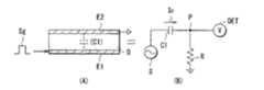
まず最初に、図1ないし図3を参照して、本実施の形態のタッチセンサ付き表示装置におけるタッチ検出方式の基本原理を表すものである。このタッチ検出方式は、静電容量型タッチセンサとして具現化されるものであり、図1(A)に示したように、誘電体Dを挟んで互いに対向配置された一対の電極(駆動電極E1および検出電極E2)を用い、容量素子を構成する。この構造は、図1(B)に示した等価回路として表される。駆動電極E1、検出電極E2および誘電体Dによって容量素子C1が構成される。容量素子C1は、その一端が交流信号源Sに接続され、他端Pは抵抗Rを介して接地されると共に電圧検出器DETに接続される。交流信号源Sから駆動電極E1(容量素子C1の一端)に所定の周波数(例えば数kHz〜十数kHz程度)の交流矩形波Sg(図3(B))を印加すると、検出電極E2(容量素子C1の他端P)に、図3(A)に示したような出力波形(検出信号Vdet )が現れる。なお、この交流矩形波Sgは、後述するコモン駆動信号Vcom に相当するものである。 First, referring to FIGS. 1 to 3, the basic principle of the touch detection method in the display device with a touch sensor according to the present embodiment will be described. This touch detection method is embodied as a capacitive touch sensor, and as shown in FIG. 1A, a pair of electrodes (drive electrodes E1) arranged opposite to each other with a dielectric D interposed therebetween. And the detection electrode E2) to form a capacitive element. This structure is expressed as an equivalent circuit shown in FIG. The drive element E1, the detection electrode E2, and the dielectric D constitute a capacitive element C1. One end of the capacitive element C1 is connected to the AC signal source S, and the other end P is grounded via the resistor R and connected to the voltage detector DET. When an AC rectangular wave Sg (FIG. 3B) having a predetermined frequency (for example, about several kHz to several tens of kHz) is applied from the AC signal source S to the drive electrode E1 (one end of the capacitive element C1), the detection electrode E2 (capacitance) An output waveform (detection signal Vdet) as shown in FIG. 3A appears at the other end P) of the element C1. The AC rectangular wave Sg corresponds to a common drive signal Vcom described later.
指を接触していない状態では、図1に示したように、容量素子C1に対する充放電に伴って、容量素子C1の容量値に応じた電流I0が流れる。このときの容量素子C1の他端Pの電位波形は、例えば図3(A)の波形V0のようになり、これが電圧検出器DETによって検出される。 In a state where the finger is not in contact, as shown in FIG. 1, a current I0 corresponding to the capacitance value of the capacitive element C1 flows along with charging / discharging of the capacitive element C1. The potential waveform at the other end P of the capacitive element C1 at this time is, for example, a waveform V0 in FIG. 3A, which is detected by the voltage detector DET.
一方、指を接触した状態では、図2に示したように、指によって形成される容量素子C2が容量素子C1に直列に追加された形となる。この状態では、容量素子C1,C2に対する充放電に伴って、それぞれ電流I1,I2が流れる。このときの容量素子C1の他端Pの電位波形は、例えば図3(A)の波形V1のようになり、これが電圧検出器DETによって検出される。このとき、点Pの電位は、容量素子C1,C2を流れる電流I1,I2の値によって定まる分圧電位となる。このため、波形V1は、非接触状態での波形V0よりも小さい値となる。電圧検出器DETは、後述するように、検出した電圧を所定のしきい値電圧Vthと比較し、このしきい値電圧以下であれば非接触状態と判断する一方、しきい値電圧以上であれば接触状態と判断する。このようにして、タッチ検出が可能となる。 On the other hand, when the finger is in contact, as shown in FIG. 2, the capacitive element C2 formed by the finger is added in series to the capacitive element C1. In this state, currents I1 and I2 flow with charging / discharging of the capacitive elements C1 and C2, respectively. The potential waveform at the other end P of the capacitive element C1 at this time is, for example, a waveform V1 in FIG. 3A, and this is detected by the voltage detector DET. At this time, the potential at the point P is a divided potential determined by the values of the currents I1 and I2 flowing through the capacitive elements C1 and C2. For this reason, the waveform V1 is smaller than the waveform V0 in the non-contact state. As will be described later, the voltage detector DET compares the detected voltage with a predetermined threshold voltage Vth, and determines that it is in a non-contact state if it is below this threshold voltage, while it is above the threshold voltage. It is determined that the contact state. In this way, touch detection is possible.
[第1の実施の形態]
図4は、本実施の形態のタッチセンサ付き表示装置の要部断面構造を表すものである。このタッチセンサ付き表示装置は、表示素子として液晶表示素子を用いると共に、この液晶表示素子に元々備えられている電極の一部(後述する共通電極43)および表示用駆動信号(後述するコモン駆動信号Vcom )を兼用して静電容量型タッチセンサを構成したものである。[First Embodiment]
FIG. 4 illustrates a cross-sectional structure of a main part of the display device with a touch sensor according to this embodiment. This display device with a touch sensor uses a liquid crystal display element as a display element, and part of electrodes originally provided in the liquid crystal display element (a
図4に示したように、このタッチセンサ付き表示装置は、画素基板2と、この画素基板2に対向して配置された対向基板4と、画素基板2と対向基板4との間に挿設された液晶層6とを備えている。 As shown in FIG. 4, the display device with a touch sensor includes a pixel substrate 2, a counter substrate 4 disposed to face the pixel substrate 2, and the pixel substrate 2 and the counter substrate 4. The
画素基板2は、回路基板としてのTFT基板21と、このTFT基板21上にマトリクス状に配設された複数の画素電極22とを有する。TFT基板21には、各画素電極22を駆動するための図示しない表示ドライバやTFT(薄膜トランジスタ)のほか、各画素電極に画素信号を供給するソース線や、各TFTを駆動するゲート線等の配線が形成されている。TFT基板21にはまた、後述するタッチ検出動作を行う検出回路(図6)が形成されていてもよい。 The pixel substrate 2 includes a
対向基板4は、ガラス基板41と、このガラス基板41の一方の面に形成されたカラーフィルタ42と、このカラーフィルタ42の上に形成された共通電極43とを有する。カラーフィルタ42は、例えば赤(R)、緑(G)、青(B)の3色のカラーフィルタ層を周期的に配列して構成したもので、各表示画素(画素電極22)ごとにR、G、Bの3色が1組として対応付けられている。共通電極43は、タッチ検出動作を行うタッチセンサの一部を構成するセンサ用駆動電極としても兼用されるものであり、図1における駆動電極E1に相当する。 The counter substrate 4 includes a
共通電極43は、コンタクト導電柱7によってTFT基板21と連結されている。このコンタクト導電柱7を介して、TFT基板21から共通電極43に交流矩形波形のコモン駆動信号Vcom が印加されるようになっている。このコモン駆動信号Vcom は、画素電極22に印加される画素電圧とともに各画素の表示電圧を画定するものであるが、タッチセンサの駆動信号としても兼用されるものであり、図1の駆動信号源Sから供給される交流矩形波Sgに相当する。 The
ガラス基板41の他方の面には、センサ用検出電極44が形成され、さらに、このセンサ用検出電極44の上には、偏光板45が配設されている。センサ用検出電極44は、タッチセンサの一部を構成するもので、図1における検出電極E2に相当する。 A
液晶層6は、電界の状態に応じてそこを通過する光を変調するものであり、例えば、TN(ツイステッドネマティック)、VA(垂直配向)、ECB(電界制御複屈折)等の各種モードの液晶が用いられる。 The
なお、液晶層6と画素基板2との間、および液晶層6と対向基板4との間には、それぞれ配向膜が配設され、また、画素基板2の下面側には入射側偏光板が配置されるが、ここでは図示を省略している。 An alignment film is provided between the
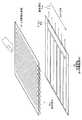
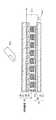
図5は、対向基板4における共通電極43およびセンサ用検出電極44の一構成例を斜視状態にて表したものである。この例では、共通電極43は、図の左右方向に延在する複数のストライプ状の電極パターンに分割されている。各電極パターンには、ドライバ43Dによってコモン駆動信号Vcom が順次供給され、時分割的に線順次走査駆動が行われるようになっている。一方、センサ用検出電極44は、共通電極43の電極パターンの延在方向と直交する方向に延びる複数のストライプ状の電極パターンから構成されている。センサ用検出電極44の各電極パターンからは、それぞれ、検出信号Vdet が出力され、図6に示した検出回路8に入力されるようになっている。 FIG. 5 illustrates a configuration example of the
図6は、タッチ検出動作を行う検出回路8の一構成例を表すものである。この検出回路8は、信号増幅用のオペアンプ81と、高域をカットし低域を通過させるローパスフィルタ(LPF)82と、高域を通過させるハイパスフィルタ(HPF)83と、整流平滑部84と、コンパレータ85とを有する。オペアンプ81の正入力端(+)には、入力端子Tinが接続され、ここから検出信号Vdet が入力されるようになっている。オペアンプ81の出力端は、LPF82を介して整流平滑部84に接続されている。LPF82にはHPF83が接続されている。LPF82は、抵抗82Rとキャパシタ82Cとを並列接続した構成であり、HPF83は、接地との間に抵抗83Rとキャパシタ83Cとを直列接続した構成である。LPF82とHPF83との接続点はオペアンプ81の負入力端(−)に接続されている。整流平滑部84は、半波整流用のダイオード84Dからなる整流部と、接地との間に抵抗84Rおよびキャパシタ82Cを並列接続してなる平滑部とを含む。整流平滑部84の出力端はコンパレータ85の正入力端(+)に接続されている。このコンパレータ85の負入力端(−)には所定のしきい値電圧Vth(図3参照)が入力されている。コンパレータ85の出力端は出力端子Tout に接続され、ここから検出結果(タッチされたか否か)が出力されるようになっている。 FIG. 6 illustrates a configuration example of the detection circuit 8 that performs the touch detection operation. The detection circuit 8 includes an
このような構成の検出回路8は、次のように動作する。入力端子Tinに入力された検出信号Vdet は、オペアンプ81によって増幅されたのち、その低周波成分はLPF82を通過し、高周波成分はHPF83を介して除去される。LPF82を通過した低周波の交流成分は、整流平滑部84のダイオード84Dによって半波整流されたのち、平滑化されてレベル信号となり、コンパレータ85に入力される。コンパレータ85は、入力されたレベル信号をしきい値電圧Vthと比較し、しきい値電圧Vth以下であったときに、タッチ検出信号を出力するようになっている。 The detection circuit 8 having such a configuration operates as follows. After the detection signal Vdet input to the input terminal Tin is amplified by the
なお、検出回路8は、対向基板4上の周辺領域(非表示領域または額縁領域)に形成するようにしてもよいし、あるいは、画素基板2上の周辺領域に形成するようにしてもよい。但し、画素基板2上に形成すれば、元々画素基板2上に形成されている表示制御用の各種回路素子等との集積化が図れるので、回路の集積化による簡略化という観点でより好ましい。この場合には、コンタクト導電柱7と同様のコンタクト導電柱(図示せず)によって、センサ用検出電極44の各電極パターンと画素基板2の検出回路8との間を接続し、検出信号Vdet をセンサ用検出電極44から検出回路8に伝送するようにすればよい。 The detection circuit 8 may be formed in a peripheral region (non-display region or frame region) on the counter substrate 4 or may be formed in a peripheral region on the pixel substrate 2. However, if it is formed on the pixel substrate 2, it can be integrated with various circuit elements for display control originally formed on the pixel substrate 2, so that it is more preferable from the viewpoint of simplification by circuit integration. In this case, a contact conductive column (not shown) similar to the contact
次に、以上のような構成のタッチセンサ付き表示装置の動作を説明する。 Next, the operation of the display device with a touch sensor configured as described above will be described.
画素基板2の表示ドライバ(図示せず)は、共通電極43の各電極パターンに対してコモン駆動信号Vcom を線順次で供給する。表示ドライバはまた、ソース線を介して画素電極22へ画素信号を供給すると共に、これに同期して、ゲート線を介して各画素電極のTFTのスイッチングを線順次で制御する。これにより、液晶層6には、画素ごとに、コモン駆動信号Vcom と各画素信号とにより定まる縦方向(基板に垂直な方向)の電界が印加されて液晶状態の変調が行われる。このようにして、いわゆる反転駆動による表示が行われる。 A display driver (not shown) of the pixel substrate 2 supplies a common drive signal Vcom to each electrode pattern of the
一方、対向基板4の側では、共通電極43の各電極パターンと、センサ用検出電極44の各電極パターンとの交差部分にそれぞれ容量素子C1が形成される。共通電極43の各電極パターンにコモン駆動信号Vcom を時分割的に順次印加していくと、その印加された共通電極43の電極パターンとセンサ用検出電極44の各電極パターンとの交差部分に形成されている一列分の容量素子C1の各々に対する充放電が行われる。その結果、容量素子C1の容量値に応じた大きさの検出信号Vdet が、センサ用検出電極44の各電極パターンからそれぞれ出力される。対向基板4の表面にユーザの指が触れられていない状態においては、この検出信号Vdet の大きさはほぼ一定となる。コモン駆動信号Vcom のスキャンに伴い、充放電の対象となる容量素子C1の列が線順次的に移動していく。 On the other hand, on the side of the counter substrate 4, capacitive elements C <b> 1 are formed at intersections between the electrode patterns of the
ここで、対向基板4の表面のいずれかの場所にユーザの指が触れると、そのタッチ箇所に元々形成されている容量素子C1に、指による容量素子C2が付加される。その結果、そのタッチ箇所がスキャンされた時点(すなわち、共通電極43の電極パターンのうち、そのタッチ箇所に対応する電極パターンにコモン駆動信号Vcom が印加されたとき)の検出信号Vdet の値が他の箇所よりも小さくなる。検出回路8(図6)は、この検出信号Vdet をしきい値電圧Vthと比較して、しきい値電圧Vth以下の場合に、その箇所をタッチ箇所として判定する。このタッチ箇所は、コモン駆動信号Vcom の印加タイミングと、しきい値電圧Vth以下の検出信号Vdet の検出タイミングとから割り出すことができる。 Here, when a user's finger touches any location on the surface of the counter substrate 4, the capacitive element C <b> 2 by the finger is added to the capacitive element C <b> 1 originally formed at the touched location. As a result, the value of the detection signal Vdet at the time when the touch location is scanned (that is, when the common drive signal Vcom is applied to the electrode pattern corresponding to the touch location among the electrode patterns of the common electrode 43) It becomes smaller than the part. The detection circuit 8 (FIG. 6) compares the detection signal Vdet with the threshold voltage Vth, and determines that the location is a touch location when it is equal to or lower than the threshold voltage Vth. This touch location can be determined from the application timing of the common drive signal Vcom and the detection timing of the detection signal Vdet below the threshold voltage Vth.
このように、本実施の形態によれば、液晶表示素子に元々備えられている共通電極43を、駆動電極と検出電極とからなる一対のタッチセンサ用電極のうちの一方として兼用すると共に、表示用駆動信号としてのコモン駆動信号Vcom を、タッチセンサ用駆動信号として共用するようにして静電容量型タッチセンサを構成したので、新たに設ける電極はセンサ用検出電極44だけでよく、また、タッチセンサ用駆動信号を新たに用意する必要がない。したがって、構成が簡単である。 As described above, according to the present embodiment, the
また、従来のタッチパネル付き表示装置(特許文献1)では、センサに流れる電流の大きさを正確に測定し、その測定値に基づいてタッチ位置をアナログ演算により求めるようにしているのに対し、本実施の形態では、タッチの有無に応じた電流の相対変化(電位変化)の有無をデジタル的に検知するだけでよいので、簡単な検出回路構成で検出精度を高めることができる。また、コモン駆動信号Vcom の印加用に元々設けられている共通電極43と、新たに設けたセンサ用検出電極44との間に静電容量を形成し、この静電容量が利用者の指の接触によって変化することを利用してタッチ検出を行うようにしたので、利用者の電位が不定であることが多いモバイル機器用途にも適合可能である。 Further, in the conventional display device with a touch panel (Patent Document 1), the magnitude of the current flowing through the sensor is accurately measured, and the touch position is obtained by analog calculation based on the measured value. In the embodiment, since it is only necessary to digitally detect the presence / absence of a relative change (potential change) in accordance with the presence / absence of a touch, the detection accuracy can be improved with a simple detection circuit configuration. Further, a capacitance is formed between the
また、センサ用検出電極44を複数の電極パターンに分割して個別に時分割的に駆動するようにしたので、タッチ位置の検出も可能になる。 In addition, since the
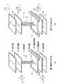
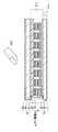
なお、上記説明では、図5に示したように、共通電極43およびセンサ用検出電極44の両方とも、互いに交差するように延在する複数の電極パターンとして形成するようにしたが、これには限定されない。例えば図7に示したように、共通電極43を一面ベタの単一電極として形成すると共に、センサ用検出電極44を、マトリクス状に配設された複数の個別電極として形成するようにしてもよい。この場合には、センサ用検出電極44を構成する各個別電極からの検出信号Vdet によって、直ちにタッチ位置を割り出すことができる。 In the above description, as shown in FIG. 5, both the
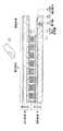
あるいは、図8に示したように、共通電極43を、図5と同様に、ストライプ状に分割された複数の電極パターンとして形成すると共に、センサ用検出電極44については、図7と同様に、マトリクス状に配設された複数の個別電極として形成するようにしてもよい。この場合においても、共通電極43の複数の電極パターンをコモン駆動信号Vcom で順次スキャンしながら検出を行うことができる。 Alternatively, as shown in FIG. 8, the
[第2の実施の形態]
次に、第2の実施の形態について説明する。本実施の形態は、上記第1の実施の形態の場合とは異なり、表示素子として横電界モードの液晶素子を用いるようにしたものである。[Second Embodiment]
Next, a second embodiment will be described. In the present embodiment, unlike the first embodiment, a liquid crystal element in a horizontal electric field mode is used as a display element.
図9は、本実施の形態のタッチセンサ付き表示装置の要部断面構造を表し、図10はその斜視構造を表すものである。これらの図で、上記の図4と同一部分には同一の符号を付し、適宜説明を省略する。 FIG. 9 illustrates a cross-sectional structure of a main part of the display device with a touch sensor according to the present embodiment, and FIG. 10 illustrates a perspective structure thereof. In these drawings, the same parts as those in FIG. 4 are denoted by the same reference numerals, and description thereof will be omitted as appropriate.
本実施の形態のタッチセンサ付き表示装置は、画素基板2Aと、この画素基板2Aに対向して配置された対向基板4Aと、画素基板2Aと対向基板4Aとの間に挿設された液晶層6とを備えている。 The display device with a touch sensor according to the present embodiment includes a
画素基板2Aは、TFT基板21と、このTFT基板21上に配設された共通電極43と、この共通電極43の上に絶縁層23を介してマトリクス状に配設された複数の画素電極22とを有する。TFT基板21には、各画素電極22を駆動するための図示しない表示ドライバやTFTのほか、各画素電極に画素信号を供給するソース線や、各TFTを駆動するゲート線等の配線が形成されている。TFT基板21にはまた、タッチ検出動作を行う検出回路(図6)が形成されている。共通電極43は、タッチ検出動作を行うタッチセンサの一部を構成するセンサ用駆動電極としても兼用されるものであり、図1における駆動電極E1に相当する。 The pixel substrate 2 </ b> A includes a
対向基板4Aは、ガラス基板41と、このガラス基板41の一方の面に形成されたカラーフィルタ42とを有する。ガラス基板41の他方の面には、センサ用検出電極44が形成され、さらに、このセンサ用検出電極44の上に偏光板45が配設されている。センサ用検出電極44は、タッチセンサの一部を構成するもので、図1における検出電極E2に相当する。センサ用検出電極44は、図5,図7または図8に示したように、複数の電極パターンに分割されて構成される。センサ用検出電極44は、薄膜プロセスにより対向基板4Aの上に直接形成してもよいが、間接的に形成してもよい。この場合には、タッチ検出電極44を図示しないフィルム基体上に形成すると共に、このタッチ検出電極44の形成されたフィルム基体を対向基板4Aの表面に貼り付けるようにすればよい。この場合、ガラスと偏光板の間だけでなく偏光板の上面に貼り付けることも可能であり、さらには偏光板を構成するフィルム内に作成してもよい。 The counter substrate 4 </ b> A includes a
共通電極43は、TFT基板21から交流矩形波形のコモン駆動信号Vcom が印加されるようになっている。このコモン駆動信号Vcom は、画素電極22に印加される画素電圧とともに各画素の表示電圧を画定するものであるが、タッチセンサの駆動信号としても兼用されるものであり、図1の駆動信号源Sから供給される交流矩形波Sgに相当する。 A common drive signal Vcom having an AC rectangular waveform is applied to the
液晶層6は、電界の状態に応じてそこを通過する光を変調するものであり、例えば、FFS(フリンジフィールドスイッチング)モードや、IPS(インプレーンスイッチング)モード等の横電界モードの液晶が用いられる。 The
画素基板2Aにおける共通電極43および対向基板4Aにおけるセンサ用検出電極44の構成は、例えば図5に示したものと同様であり、両方とも、互いに交差するように延在する複数の電極パターンとして形成されている。但し、上記の図7または図8に示したような構成であってもよい。 The configurations of the
図10を参照して、より詳細に説明する。ここに示したようなFFSモードの液晶素子においては、画素基板2A上に形成された共通電極43の上に、絶縁層23を介して、櫛歯状にパターニングされた画素電極22が配置され、これを覆うように配向膜26が形成される。この配向膜26と、対向基板4A側の配向膜46との間に、液晶層6が挟持される。2枚の偏光板24,45は、クロスニコルの状態で配置される。2枚の配向膜26,46のラビング方向は、2枚の偏光板24,45の一方の透過軸と一致している。図10では、ラビング方向が出射側の偏光板45の透過軸と一致している場合を図示してある。さらに、2枚の配向膜26,46のラビング方向および偏光板45の透過軸の方向は、液晶分子が回転する方向が規定される範囲で、画素電極22の延設方向(櫛歯の長手方向)とほぼ平行に設定されている。 This will be described in more detail with reference to FIG. In the FFS mode liquid crystal element as shown here, the
次に、以上のような構成のタッチセンサ付き表示装置の動作を説明する。 Next, the operation of the display device with a touch sensor configured as described above will be described.
ここではまず、図10および図11を参照して、FFSモードの液晶素子の表示動作原理について簡単に説明する。ここで、図11は液晶素子の要部断面を拡大して表したものである。これらの図で、(A)は電界非印加時、(B)は電界印加時における液晶素子の状態を示す。 Here, first, the display operation principle of the FFS mode liquid crystal element will be briefly described with reference to FIGS. Here, FIG. 11 shows an enlarged cross-sectional view of the main part of the liquid crystal element. In these figures, (A) shows the state of the liquid crystal element when no electric field is applied, and (B) shows the state of the liquid crystal element when the electric field is applied.
共通電極43と画素電極22との間に電圧を印加していない状態では(図10(A)、図11(A))、液晶層6を構成する液晶分子61の軸が入射側の偏光板24の透過軸と直交し、かつ、出射側の偏光板45の透過軸と平行な状態となる。このため、入射側の偏光板24を透過した入射光hは、液晶層6内において位相差を生じることなく出射側の偏光板45に達し、ここで吸収されるため、黒表示となる。一方、共通電極43と画素電極22との間に電圧を印加した状態では(図10(B)、図11(B))、液晶分子61の配向方向が、画素電極間に生じる横電界Eにより、画素電極22の延設方向に対して斜め方向に回転する。この際、液晶層6の厚み方向の中央に位置する液晶分子61が約45度回転するように白表示時の電界強度を最適化する。これにより、入射側の偏光板24を透過した入射光hには、液晶層6内を透過する間に位相差が生じ、90度回転した直線偏光となり、出射側の偏光板45を通過するため、白表示となる。 In a state where no voltage is applied between the
次にタッチセンサ付き表示装置の表示制御動作およびタッチ検出動作を説明する。これらの動作は、上記第1の実施の形態における動作と同様なので、適宜省略する。 Next, a display control operation and a touch detection operation of the display device with a touch sensor will be described. Since these operations are the same as those in the first embodiment, they will be omitted as appropriate.
画素基板2Aの表示ドライバ(図示せず)は、共通電極43の各電極パターンに対してコモン駆動信号Vcom を線順次で供給する。表示ドライバはまた、ソース線を介して画素電極22へ画素信号を供給すると共に、これに同期して、ゲート線を介して各画素電極のTFTのスイッチングを線順次で制御する。これにより、液晶層6には、画素ごとに、コモン駆動信号Vcom と各画素信号とにより定まる横方向(基板に平行な方向)の電界が印加されて液晶状態の変調が行われる。このようにして、いわゆる反転駆動による表示が行われる。 A display driver (not shown) of the pixel substrate 2 </ b> A supplies a common drive signal Vcom to each electrode pattern of the
一方、対向基板4Aの側では、共通電極43の各電極パターンにコモン駆動信号Vcom を時分割的に順次印加していくと、その印加された共通電極43の電極パターンとセンサ用検出電極44の各電極パターンとの交差部分に形成されている一列分の容量素子C1の各々に対する充放電が行われ、容量素子C1の容量値に応じた大きさの検出信号Vdet が、センサ用検出電極44の各電極パターンからそれぞれ出力される。対向基板4Aの表面にユーザの指が触れられていない状態においては、この検出信号Vdet の大きさはほぼ一定となる。対向基板4Aの表面のいずれかの場所にユーザの指が触れると、そのタッチ箇所に元々形成されている容量素子C1に、指による容量素子C2が付加される結果、そのタッチ箇所がスキャンされた時点の検出信号Vdet の値が他の箇所よりも小さくなる。検出回路8(図6)は、この検出信号Vdet をしきい値電圧Vthと比較して、しきい値電圧Vth以下の場合に、その箇所をタッチ箇所として判定する。このタッチ箇所は、コモン駆動信号Vcom の印加タイミングと、しきい値電圧Vth以下の検出信号Vdet の検出タイミングとから割り出される。 On the other hand, on the
このように、本実施の形態によれば、上記第1の実施の形態(図5)の場合と同様に、液晶表示素子に元々備えられている共通電極43を、駆動電極と検出電極とからなる一対のタッチセンサ用電極のうちの一方として兼用すると共に、表示用駆動信号としてのコモン駆動信号Vcom を、タッチセンサ用駆動信号として共用して静電容量型タッチセンサを構成したので、新たに設ける電極はセンサ用検出電極44だけでよく、また、タッチセンサ用駆動信号を新たに用意する必要がない。したがって、構成が簡単である。 As described above, according to the present embodiment, as in the case of the first embodiment (FIG. 5), the
特に、本実施の形態では、タッチセンサ用駆動電極としての共通電極43が画素基板2の側(TFT基板21の上)に設けられた構造を有していることから、TFT基板21から共通電極43にコモン駆動信号Vcom を供給することが極めて容易であると共に、必要な回路や電極パターンおよび配線等を画素基板2に集中させることができ、回路の集積化が図られる。したがって、上記第1の実施の形態(図5)において必要であった、画素基板2側から対向基板4側へのコモン駆動信号Vcom の供給経路(コンタクト導電柱7)が不要となり、構造がより簡単になる。 In particular, in the present embodiment, since the
なお、検出回路8(図6)は、対向基板4上の周辺領域(非表示領域または額縁領域)に形成するようにしてもよいが、画素基板2上の周辺領域に形成するのが好ましい。画素基板2上に形成すれば、元々画素基板2上に形成されている表示制御用の各種回路素子等との集積化が図れるからである。この場合には、例えば図12に示したように、周辺領域にコンタクト導電柱7Aを形成して、画素基板2に形成された検出回路8(図示せず)と、対向基板4のカラーフィルタ42の表面との間を接続することにより、センサ用検出電極44と検出回路8との間に容量結合経路を形成し、この容量結合経路を介して検出信号Vdet をセンサ用検出電極44から検出回路8に伝送するようにすればよい。但し、この場合には、センサ用検出電極44がフローティング状態になってしまうため、これを回避すべく、高抵抗10を介してセンサ用検出電極44を接地に接続することが好ましい。なお、このように接地することは、静電気を接地に逃がすことができる点でもメリットがある。 The detection circuit 8 (FIG. 6) may be formed in the peripheral region (non-display region or frame region) on the counter substrate 4, but is preferably formed in the peripheral region on the pixel substrate 2. This is because if formed on the pixel substrate 2, integration with various circuit elements for display control originally formed on the pixel substrate 2 can be achieved. In this case, for example, as shown in FIG. 12, a contact
[変形例]
第2の実施の形態では、センサ用検出電極44をガラス基板41の表面側(液晶層6と反対側)に設けるようにしたが、次のような変形が可能である。[Modification]
In the second embodiment, the
例えば図13に示したように、センサ用検出電極44をカラーフィルタ42よりも液晶層6の側に設けるようにしてもよい。 For example, as shown in FIG. 13, the
あるいは、図14に示したように、センサ用検出電極44をガラス基板41とカラーフィルタ42との間に設けたほうが好ましい。横電界モードの場合、縦方向に電極があると縦方向に電界がかかり、液晶が立ち上がってしまい視野角等が大きく悪化してしまう。カラーフィルター42等の誘電体をはさんでセンサ用検出電極44を配置すれば、この問題は大きく低減することができる。なお、この場合には、例えば図15に示したように、コンタクト導電柱7Bによって、画素基板2に形成された検出回路8(図示せず)と、対向基板4のセンサ用検出電極44との間を接続することにより、センサ用検出電極44と検出回路8との間に導電経路を形成し、この導電経路を介して検出信号Vdet をセンサ用検出電極44から検出回路8に伝送するようにすればよい。 Alternatively, as shown in FIG. 14, it is preferable to provide the
[第3の実施の形態]
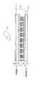
上記第1および第2の実施の形態では、センサ用検出電極44を表示領域に配設するようにしたが、本実施の形態は、図16,図17に示したように、センサ用検出電極44を表示領域Dの周りの領域(額縁領域F)に設けるようにしたものである。なお、図17は本実施の形態のタッチセンサ付き表示装置の平面構成を表し、図16は、図17におけるA−A矢視断面を表す。[Third Embodiment]
In the first and second embodiments, the
このタッチセンサ付き表示装置では、画素基板2B側に共通電極43およびセンサ用検出電極44の両方が形成され、対向基板4側にはいずれの電極も配設されていない。具体的には、表示領域Dの全体にわたってTFT基板21上に共通電極43が形成される一方、額縁領域Fにのみ、TFT基板21上にセンサ用検出電極44が配設されている。センサ用検出電極44は、複数の個別電極群として形成される。各個別電極は、例えば表示アプリケーションの各種機能に対応した操作ボタンとして割り当てられる。センサ用検出電極44の各個別電極は、スキャン信号線52によってスイッチング制御されるTFT50のソース・ドレインを介してセンサ用検出信号線51に接続されるようになっている。スキャン信号線52やTFT50を画素の駆動回路と同時に形成すると共に、各個別電極を順次時分割的にスキャンするように構成することにより、検出回路を分割数持つ必要がなくなり非常に効率的である。 In the display device with a touch sensor, both the
このような構成のタッチセンサ付き表示装置では、センサ用検出電極44の各個別電極は、共通電極43の形成面と同じ平面上に、共通電極43から隔てて配設されていることから、センサ用検出電極44の各個別電極と共通電極43との間には横方向の容量結合が生じ、容量素子C1が形成される。共通電極43(図17の例では一面ベタの電極)にコモン駆動信号Vcom が印加されると共に、スキャン信号線52によってTFT50を順次オンさせることにより、センサ用検出電極44の各個別電極から検出信号Vdet を時分割的に順次取り出す。取り出された検出信号Vdet は、センサ用検出信号線51を介して、図6に示したような構成の検出回路8(図16では図示せず)に入力される。 In the display device with a touch sensor having such a configuration, each individual electrode of the
対向基板4Dの表面にユーザの指が触れられていない状態においては、この検出信号Vdet の大きさはほぼ一定となる。一方、対向基板4Aの表面のいずれかの場所(センサ用検出電極44のいずれかの個別電極に対応した位置)にユーザの指が触れると、そのタッチ箇所に元々形成されている容量素子C1に、指による容量素子C2が付加される結果、そのタッチ箇所がスキャンされた時点の検出信号Vdet の値が小さく変化する。検出回路8(図6)は、この検出信号Vdet をしきい値電圧Vthと比較して、しきい値電圧Vth以下の場合に、その箇所をタッチ箇所として判定する。このタッチ箇所は、スキャン信号によるセンサ用検出電極44の個別電極スキャンのタイミングと、しきい値電圧Vth以下の検出信号Vdet の検出タイミングとから割り出される。 When the user's finger is not touching the surface of the counter substrate 4D, the magnitude of the detection signal Vdet is substantially constant. On the other hand, when a user's finger touches any location on the surface of the
このように、本実施の形態によれば、共通電極43およびセンサ用検出電極44の両方を画素基板2の側に配設するようにしたので、TFT基板21に形成したセンサ駆動回路(図示せず)と共通電極43との間のコモン駆動信号Vcom の伝送経路や、センサ用検出電極44と検出回路8との間の検出信号Vdet の伝送経路を、コンタクト導電柱を介することなく容易に形成することができる。したがって、共通電極43およびセンサ用検出電極44、表示用回路、タッチセンサの駆動回路および検出回路をTFT基板21に集中的に集積化することが極めて容易となる。 As described above, according to the present embodiment, since both the
なお、本実施の形態のように、共通電極43とセンサ用検出電極44とを並べて配設して、両者間に横方向容量結合による容量素子C1を形成するようにした場合には、共通電極43からTFT基板21内部の回路素子(TFT50等)へのノイズ飛びが問題になる場合がある。そこで、これを防ぐために、図18に示したように、センサ用検出電極44の下側にシールド電極53を設けることが好ましい。但し、上記シールド層は、特に専用の新しい層を設けるのではなく、金属配線や画素電極を構成する透明電極膜を流用することも可能である。 In the case where the
[変形例]
上記第3の実施の形態では、TFT基板21上に共通電極43とセンサ用検出電極44とを並べて配設し、横方向容量結合により容量素子C1を形成するようにしたが、これとは異なり、縦方向容量結合により容量素子C1を形成することも可能である。例えば図19に示したように、共通電極43をTFT基板21上の表示領域Dのみならず額縁領域Fにまで延在させると共に、センサ用検出電極44を、TFT基板21の額縁領域Fにおいて、共通電極43と異なる階層の電極層として共通電極43に対向するように形成する。これにより、共通電極43とセンサ用検出電極44との間に容量素子C1が形成される。この場合には、センサ用検出電極44とTFT基板21との間を結ぶコンタクト導電柱7Cを設け、これにより、センサ用検出電極44からの検出信号Vdet をTFT基板21側に伝送するようにすればよい。[Modification]
In the third embodiment, the
以上の第1〜第3の実施の形態の説明から明らかなように、表示機能層としての液晶層のタイプに応じて、センサ用検出電極44を対向基板4の側に形成するか、あるいは画素基板2の側に形成するかを適宜選択可能であるので、構造設計の自由度が高いというメリットがある。 As is apparent from the description of the first to third embodiments, the
以上、いくつかの実施の形態を挙げて本発明を説明したが、本発明はこれらの実施の形態に限定されず、種々の変形が可能である。例えば、上記の第2、第3の実施の形態では、横電界モードとしてFFSモードの液晶素子を例に説明したが、IPSモードの液晶について同様に適用可能である。 Although the present invention has been described with reference to some embodiments, the present invention is not limited to these embodiments, and various modifications can be made. For example, in the second and third embodiments described above, the FFS mode liquid crystal element is described as an example of the transverse electric field mode, but the present invention can be similarly applied to an IPS mode liquid crystal.
また、上記実施の形態では、表示素子として液晶表示素子を用いた表示装置について説明したが、それ以外の表示素子、例えば有機EL素子を用いた表示装置にも適用可能である。 In the above embodiment, a display device using a liquid crystal display element as a display element has been described. However, the present invention can also be applied to a display device using another display element, for example, an organic EL element.
2,2A,2B,2C,2D…画素基板、21…TFT基板、22…画素電極、4,4A,4B,4C,4D,4E…対向基板、41…ガラス基板、42…カラーフィルタ、43…共通電極(兼センサ用駆動電極)、43D…ドライバ、44…センサ用検出電極、45…偏光板、50…TFT、51…センサ用検出信号線、52…スキャン信号線、53…シールド電極、6…液晶層、7,7A,7B,7C…コンタクト導電柱、8…検出回路、81…オペアンプ、82…LPF、83…HPF、84…整流平滑部、85…コンパレータ、C1,C2…容量素子、Sg …交流矩形波、E1…駆動電極、E2…検出電極、Vcom …コモン駆動信号、Vdet …検出信号、Vth…しきい値電圧。 2, 2A, 2B, 2C, 2D ... pixel substrate, 21 ... TFT substrate, 22 ... pixel electrode, 4, 4A, 4B, 4C, 4D, 4E ... counter substrate, 41 ... glass substrate, 42 ... color filter, 43 ... Common electrode (cumulative sensor drive electrode), 43D ... driver, 44 ... sensor detection electrode, 45 ... polarizing plate, 50 ... TFT, 51 ... sensor detection signal line, 52 ... scan signal line, 53 ... shield electrode, 6 ... liquid crystal layer, 7, 7A, 7B, 7C ... contact conductive column, 8 ... detection circuit, 81 ... operational amplifier, 82 ... LPF, 83 ... HPF, 84 ... rectifying / smoothing unit, 85 ... comparator, C1, C2 ... capacitive element, Sg: AC rectangular wave, E1: Drive electrode, E2: Detection electrode, Vcom: Common drive signal, Vdet: Detection signal, Vth: Threshold voltage
Claims (14)
Translated fromJapanese前記表示画素電極と対向して設けられた共通電極と、
画像表示機能を有する表示機能層と、
画像信号に基づいて、前記表示画素電極と前記共通電極との間に表示用電圧を印加して前記表示機能層の表示機能を発揮させるように画像表示制御を行う表示制御回路と、
前記共通電極と対向して、または並んで設けられ、前記共通電極との間に静電容量を形成するタッチ検出電極と、
前記表示制御回路により前記共通電極に印加される表示用駆動電圧をタッチセンサ用駆動信号として利用し、前記タッチ検出電極から得られる検出信号に基づき、物体の接触位置を検出するタッチ検出回路と、
回路基板と、
前記回路基板と対向して配設された対向基板と
を備え、
前記回路基板には、前記表示制御回路および前記タッチ検出電極が形成されるとともに、前記共通電極および前記表示画素電極が絶縁層を介して順に積層され、
前記回路基板の前記表示画素電極と、前記対向基板との間に、前記表示機能層が挿設されている
タッチセンサ付き表示装置。A plurality of display pixel electrodes;
A common electrode provided facing the display pixel electrode;
A display function layer having an image display function;
A display control circuit that performs image display control so as to exert a display function of the display function layer by applying a display voltage between the display pixel electrode and the common electrode based on an image signal;
A touch detection electrode provided opposite to or side by side with the common electrode, and forming a capacitance between the common electrode;
A touch detection circuit that uses a display drive voltage applied to the common electrode by the display control circuit as a touch sensor drive signal and detects a contact position of an object based on a detection signal obtained from the touch detection electrode;
A circuit board;
A counter substrate disposed opposite to the circuit board;
With
On the circuit board, the display control circuit and the touch detection electrode are formed, and the common electrode and the display pixel electrode are sequentially stacked via an insulating layer,
The display functional layer is inserted between the display pixel electrode of the circuit board and the counter substrate.
Data Tchisensa with a display device.
前記タッチ検出電極が、前記回路基板上の前記表示領域を取り囲む額縁領域に、前記共通電極と同一階層の電極層として前記共通電極から隔てて形成されている
請求項1に記載のタッチセンサ付き表示装置。The common electrode is disposed inside a display area of the circuit board;
The touch detection electrode, the frame area surrounding the display area on the circuit board,that is formed at from the common electrode as the electrode layer of the common electrode and the same layer
The display device with a touch sensor according toclaim 1 .
前記タッチ検出電極が、前記回路基板の前記額縁領域において、前記共通電極と異なる階層の電極層として前記共通電極に対向して形成されている
請求項1に記載のタッチセンサ付き表示装置。The common electrode extends from the display area on the circuit board to the frame area;
The touch detection electrode, in the frame region of the circuit board,that are formed opposite to the common electrode as the electrode layer of the common electrode and the different layers
The display device with a touch sensor according toclaim 1 .
請求項1から請求項3のいずれか一項に記載のタッチセンサ付き表示装置。Isthat is disposed the shield electrode for shielding the touch detection electrode electromagnetically
The display device with a touch sensor according toany one of claims 1 to 3 .
前記表示画素電極と対向して設けられた共通電極と、
画像表示機能を有する表示機能層と、
画像信号に基づいて、前記表示画素電極と前記共通電極との間に表示用電圧を印加して前記表示機能層の表示機能を発揮させるように画像表示制御を行う表示制御回路と、
前記共通電極と対向して設けられ、前記共通電極との間に静電容量を形成するタッチ検出電極と、
前記表示制御回路により前記共通電極に印加される表示用駆動電圧をタッチセンサ用駆動信号として利用し、前記タッチ検出電極から得られる検出信号に基づき、物体の接触位置を検出するタッチ検出回路と、
回路基板と、
前記回路基板と対向して配設された対向基板と
を備え、
前記対向基板には前記タッチ検出電極が形成され、
前記回路基板には、前記表示制御回路が形成されるとともに、前記共通電極および前記表示画素電極が絶縁層を介して順に積層され、
前記回路基板の前記表示画素電極と、前記対向基板との間に、前記表示機能層が挿設されている
タッチセンサ付き表示装置。A plurality of display pixel electrodes;
A common electrode provided facing the display pixel electrode;
A display function layer having an image display function;
A display control circuit that performs image display control so as to exert a display function of the display function layer by applying a display voltage between the display pixel electrode and the common electrode based on an image signal;
A touch detection electrode for forming a capacitance between the common electrode and the counterto set the vignetting, the commonelectrode,
A touch detection circuit that uses a display drive voltage applied to the common electrode by the display control circuit as a touch sensor drive signal and detects a contact position of an object based on a detection signal obtained from the touch detection electrode;
A circuit board;
A counter substrate disposed opposite to the circuit board;
With
The touch detection electrode is formed on the counter substrate,
On the circuit board, the display control circuit is formed, and the common electrode and the display pixel electrode are sequentially stacked via an insulating layer,
The display functional layer is inserted between the display pixel electrode of the circuit board and the counter substrate.
Data Tchisensa with a display device.
請求項5に記載のタッチセンサ付き表示装置。The touch detection electrode, the counter substrate,that is disposed closer to the circuit board
The display device with a touch sensor according toclaim 5 .
請求項5に記載のタッチセンサ付き表示装置。The touch detection electrode, the counter substrate,that is disposed on the opposite side to the circuit board
The display device with a touch sensor according toclaim 5 .
請求項7に記載のタッチセンサ付き表示装置。The touch detection electrode,that is directly formed on the opposing substrate by a thin film process
The display device with a touch sensor according toclaim 7 .
請求項7に記載のタッチセンサ付き表示装置。The touch detection electrode is formed on the film substrate,that formed film substrates of the touch detection electrode is not attached to the counter substrate
The display device with a touch sensor according toclaim 7 .
請求項5に記載のタッチセンサ付き表示装置。The touch detection circuit,that is formed on the circuit board
The display device with a touch sensor according toclaim 5 .
請求項10に記載のタッチセンサ付き表示装置。Conductive path connecting thethat is formed between the touch detection circuit of the circuit board and the touch detection electrode of the counter substrate
The display device with a touch sensor according toclaim 10 .
請求項10に記載のタッチセンサ付き表示装置。Coupling capacitively coupling pathsthat are formed capacitance between the touch detection circuit of the circuit board and the touch detection electrode of the counter substrate
The display device with a touch sensor according toclaim 10 .
請求項12に記載のタッチセンサ付き表示装置。That is grounded the touch detection electrode of the counter substrate through the high-resistance
The display device with a touch sensor according toclaim 12 .
請求項1から請求項13のいずれか一項に記載のタッチセンサ付き表示装置。The display function layer is a liquid crystal layer,Ru is performed LCD in the transverse electric field mode
The display device with a touch sensor according toany one of claims 1 to 13 .
Priority Applications (13)
| Application Number | Priority Date | Filing Date | Title |
|---|---|---|---|
| JP2008087739AJP4816668B2 (en) | 2008-03-28 | 2008-03-28 | Display device with touch sensor |
| TW098109245ATWI406047B (en) | 2008-03-28 | 2009-03-20 | A display device with a touch sensor |
| CN200980000383.XACN101681221B (en) | 2008-03-28 | 2009-03-25 | Display device with touch sensor |
| PCT/JP2009/055949WO2009119664A1 (en) | 2008-03-28 | 2009-03-25 | Display device provided with touch sensor |
| KR1020097024574AKR101599072B1 (en) | 2008-03-28 | 2009-03-25 | Display device provided with touch sensor |
| US12/601,310US8786557B2 (en) | 2008-03-28 | 2009-03-25 | Display device with touch sensor |
| US14/168,871US9335875B2 (en) | 2008-03-28 | 2014-01-30 | Display device with touch sensor |
| US14/302,481US9542047B2 (en) | 2008-03-28 | 2014-06-12 | Display device with touch sensor |
| US15/226,192US10037116B2 (en) | 2008-03-28 | 2016-08-02 | Display device with touch sensor |
| US16/016,055US10768755B2 (en) | 2008-03-28 | 2018-06-22 | Display device with touch sensor |
| US16/927,599US11402682B2 (en) | 2008-03-28 | 2020-07-13 | Touch sensor device |
| US17/847,428US11686964B2 (en) | 2008-03-28 | 2022-06-23 | Touch sensor device |
| US18/315,566US12025875B2 (en) | 2008-03-28 | 2023-05-11 | Touch sensor device |
Applications Claiming Priority (1)
| Application Number | Priority Date | Filing Date | Title |
|---|---|---|---|
| JP2008087739AJP4816668B2 (en) | 2008-03-28 | 2008-03-28 | Display device with touch sensor |
Related Child Applications (1)
| Application Number | Title | Priority Date | Filing Date |
|---|---|---|---|
| JP2011152880ADivisionJP2011227923A (en) | 2011-07-11 | 2011-07-11 | Display device with touch sensor |
Publications (3)
| Publication Number | Publication Date |
|---|---|
| JP2009244958A JP2009244958A (en) | 2009-10-22 |
| JP2009244958A5 JP2009244958A5 (en) | 2009-12-03 |
| JP4816668B2true JP4816668B2 (en) | 2011-11-16 |
Family
ID=41113855
Family Applications (1)
| Application Number | Title | Priority Date | Filing Date |
|---|---|---|---|
| JP2008087739AActiveJP4816668B2 (en) | 2008-03-28 | 2008-03-28 | Display device with touch sensor |
Country Status (6)
| Country | Link |
|---|---|
| US (8) | US8786557B2 (en) |
| JP (1) | JP4816668B2 (en) |
| KR (1) | KR101599072B1 (en) |
| CN (1) | CN101681221B (en) |
| TW (1) | TWI406047B (en) |
| WO (1) | WO2009119664A1 (en) |
Cited By (5)
| Publication number | Priority date | Publication date | Assignee | Title |
|---|---|---|---|---|
| JP2009258182A (en)* | 2008-04-11 | 2009-11-05 | Sony Corp | Display device and method of driving the same |
| US9599849B2 (en) | 2014-02-06 | 2017-03-21 | Japan Display Inc. | Display device with a touch sensor |
| US10055058B2 (en) | 2014-02-28 | 2018-08-21 | Toppan Printing Co., Ltd. | Liquid crystal display device with touch sensing function and plurality of transparent electrode patterns |
| US10126585B2 (en) | 2014-02-28 | 2018-11-13 | Toppan Printing Co., Ltd. | Liquid crystal display device |
| US10386950B2 (en) | 2015-07-22 | 2019-08-20 | Sharp Kabushiki Kaisha | Touch-panel-equipped display device and method for manufacturing touch-panel-equipped display device |
Families Citing this family (366)
| Publication number | Priority date | Publication date | Assignee | Title |
|---|---|---|---|---|
| US7663607B2 (en) | 2004-05-06 | 2010-02-16 | Apple Inc. | Multipoint touchscreen |
| CN102981678B (en) | 2006-06-09 | 2015-07-22 | 苹果公司 | Touch screen liquid crystal display |
| CN104965621B (en) | 2006-06-09 | 2018-06-12 | 苹果公司 | Touch screen LCD and its operating method |
| US9710095B2 (en) | 2007-01-05 | 2017-07-18 | Apple Inc. | Touch screen stack-ups |
| JP4816668B2 (en)* | 2008-03-28 | 2011-11-16 | ソニー株式会社 | Display device with touch sensor |
| TW200942459A (en)* | 2008-04-07 | 2009-10-16 | rui-yang Zhang | Auto-inflatable capsule |
| JP5206250B2 (en)* | 2008-05-02 | 2013-06-12 | セイコーエプソン株式会社 | Display device and electronic device |
| KR101350573B1 (en)* | 2008-12-30 | 2014-01-10 | 엘지디스플레이 주식회사 | Electrophoresis display device |
| US8643624B2 (en)* | 2009-03-18 | 2014-02-04 | Synaptics Incorporated | Capacitive sensing using a segmented common voltage electrode of a display |
| JP5366051B2 (en)* | 2009-04-20 | 2013-12-11 | 株式会社ジャパンディスプレイ | Information input device, display device |
| TWI431362B (en)* | 2009-05-29 | 2014-03-21 | Japan Display West Inc | Touch sensor, display and electronic device |
| US8456586B2 (en)* | 2009-06-11 | 2013-06-04 | Apple Inc. | Portable computer display structures |
| KR101073194B1 (en) | 2009-10-06 | 2011-10-12 | 삼성모바일디스플레이주식회사 | Liquid Crystal Display with a Built-in Touch Screen |
| KR101073345B1 (en) | 2009-10-06 | 2011-10-14 | 삼성모바일디스플레이주식회사 | Liquid Crystal Display with a Built-in Touch Screen |
| CN102043184B (en)* | 2009-10-09 | 2013-10-09 | Lg化学株式会社 | Integrated touch polarizer and touch panel comprising the same |
| JP5439114B2 (en)* | 2009-10-21 | 2014-03-12 | 株式会社ジャパンディスプレイ | Capacitance type input device and electro-optical device with input device |
| US8408780B2 (en) | 2009-11-03 | 2013-04-02 | Apple Inc. | Portable computer housing with integral display |
| US8743309B2 (en) | 2009-11-10 | 2014-06-03 | Apple Inc. | Methods for fabricating display structures |
| CN102096489B (en)* | 2009-12-11 | 2013-04-03 | 胜华科技股份有限公司 | Touch Display Panel |
| TWI420197B (en)* | 2010-01-21 | 2013-12-21 | Tpk Touch Solutions Inc | Embedded touch sensitive display and a method of manufacturing the same |
| CN201622554U (en)* | 2010-02-04 | 2010-11-03 | 深圳市汇顶科技有限公司 | Capacitance touch sensor, touch detection device, and touch control terminal |
| ES2655729T3 (en)* | 2010-02-10 | 2018-02-21 | Microchip Technology Germany Gmbh | System and procedure for generating a correlated signal with a manual input operation |
| TWI420117B (en)* | 2010-02-11 | 2013-12-21 | Novatek Microelectronics Corp | Capacitance sensing apparatus and touch sensing system |
| CN102884496B (en)* | 2010-02-26 | 2017-06-30 | 辛纳普蒂克斯公司 | Modify demodulation to avoid interference |
| KR101633601B1 (en)* | 2010-03-04 | 2016-06-27 | 엘지디스플레이 주식회사 | Liquid crystal display panel with a built-in touch screen, and liquid crystal display device having the same |
| KR101298234B1 (en) | 2010-03-19 | 2013-08-22 | 엘지디스플레이 주식회사 | In-plane switching mode liquid crystal display device having touch sensing function and method of fabricating the same |
| KR101307962B1 (en) | 2010-03-19 | 2013-09-12 | 엘지디스플레이 주식회사 | In-plane switching mode liquid crystal display device having touch sensing function and method of fabricating the same |
| JPWO2011122352A1 (en)* | 2010-03-29 | 2013-07-08 | シャープ株式会社 | Display device, pressure detection device, and display device manufacturing method |
| TWI435140B (en)* | 2010-04-09 | 2014-04-21 | Wintek Corp | Display with touch panel |
| US8941395B2 (en) | 2010-04-27 | 2015-01-27 | 3M Innovative Properties Company | Integrated passive circuit elements for sensing devices |
| JP2011233019A (en) | 2010-04-28 | 2011-11-17 | Sony Corp | Display device with touch detection function, drive circuit, drive system, and electronic equipment |
| JP5455126B2 (en) | 2010-04-28 | 2014-03-26 | 株式会社ジャパンディスプレイ | Display device with touch detection function, driving method, and electronic device |
| US9898121B2 (en) | 2010-04-30 | 2018-02-20 | Synaptics Incorporated | Integrated capacitive sensing and displaying |
| JP5523191B2 (en)* | 2010-04-30 | 2014-06-18 | 株式会社ジャパンディスプレイ | Display device with touch detection function |
| CN101825796B (en) | 2010-05-19 | 2012-06-13 | 北京富纳特创新科技有限公司 | Touch liquid crystal screen |
| KR101274649B1 (en)* | 2010-05-27 | 2013-06-12 | 엘지디스플레이 주식회사 | Liquid Crystal Display Device including Touch Panel and Method for Manufacturing the Same |
| JP5237330B2 (en)* | 2010-06-15 | 2013-07-17 | 信越ポリマー株式会社 | Sensor sheet and input device |
| KR101735386B1 (en)* | 2010-06-25 | 2017-05-30 | 엘지디스플레이 주식회사 | Liquid crystal display device having touch sensor embedded therein, method for driving the same and method for fabricating the same |
| KR20120010795A (en)* | 2010-07-27 | 2012-02-06 | 삼성전기주식회사 | Touch panel integrated electronic paper |
| JP5513308B2 (en)* | 2010-08-19 | 2014-06-04 | 株式会社ジャパンディスプレイ | Display device with touch detection function and electronic device |
| KR20120017587A (en)* | 2010-08-19 | 2012-02-29 | 삼성모바일디스플레이주식회사 | Touch Screen Panel Integrated LCD |
| JP5653686B2 (en) | 2010-08-24 | 2015-01-14 | 株式会社ジャパンディスプレイ | Display device with touch detection function |
| JP5722573B2 (en) | 2010-08-24 | 2015-05-20 | 株式会社ジャパンディスプレイ | Display device with touch detection function |
| WO2012030183A2 (en)* | 2010-09-01 | 2012-03-08 | Lee Sung Ho | Capacitive touch detection apparatus using level shift, detection method using level shift, and display device having the detection apparatus built therein |
| JP5458443B2 (en) | 2010-09-14 | 2014-04-02 | 株式会社ジャパンディスプレイ | Display device with touch detection function and electronic device |
| KR101733140B1 (en) | 2010-09-14 | 2017-05-08 | 삼성디스플레이 주식회사 | Display Device Integrated Touch Screen Panel and Fabricating Method Thereof |
| JP5667824B2 (en) | 2010-09-24 | 2015-02-12 | 株式会社ジャパンディスプレイ | Touch detection device and driving method thereof, display device with touch detection function, and electronic device |
| JP5615647B2 (en)* | 2010-09-24 | 2014-10-29 | 株式会社ジャパンディスプレイ | Display device with touch detection function and electronic device |
| JP5616184B2 (en)* | 2010-09-28 | 2014-10-29 | 株式会社ジャパンディスプレイ | Display device with touch detection function and electronic device |
| JP5766928B2 (en) | 2010-09-29 | 2015-08-19 | 株式会社ジャパンディスプレイ | Display device with touch detection function and electronic device |
| KR101188983B1 (en) | 2010-09-30 | 2012-10-08 | 삼성디스플레이 주식회사 | 3 Dimension Plat Panel Display having a Touch Screen Panel |
| KR101790977B1 (en) | 2010-10-08 | 2017-10-26 | 엘지디스플레이 주식회사 | Liquid crystal display device |
| KR101897969B1 (en)* | 2010-10-12 | 2018-09-12 | 엘지디스플레이 주식회사 | Liquid crystal display device |
| US8467177B2 (en) | 2010-10-29 | 2013-06-18 | Apple Inc. | Displays with polarizer windows and opaque masking layers for electronic devices |
| KR101230196B1 (en)* | 2010-10-29 | 2013-02-06 | 삼성디스플레이 주식회사 | Liquid Crystal Display having a Touch Screen Panel |
| KR20120045290A (en)* | 2010-10-29 | 2012-05-09 | 삼성모바일디스플레이주식회사 | Liquid crystal display integrated touch screen panel |
| KR101230146B1 (en) | 2010-10-29 | 2013-02-05 | 삼성디스플레이 주식회사 | Liquid Crystal Display integrated Touch Screen Panel and Driving Method thereof |
| CN102455536B (en)* | 2010-10-29 | 2014-11-19 | 三星显示有限公司 | Liquid crystal display with integrated touch screen panel and driving method thereof |
| US9143668B2 (en) | 2010-10-29 | 2015-09-22 | Apple Inc. | Camera lens structures and display structures for electronic devices |
| KR101755601B1 (en) | 2010-11-04 | 2017-07-10 | 삼성디스플레이 주식회사 | Liquid Crystal Display integrated Touch Screen Panel |
| KR101799029B1 (en)* | 2010-11-08 | 2017-11-20 | 삼성디스플레이 주식회사 | Liquid Crystal Display integrated Touch Screen Panel |
| WO2012063787A1 (en)* | 2010-11-10 | 2012-05-18 | シャープ株式会社 | Display device |
| JP5555142B2 (en)* | 2010-11-25 | 2014-07-23 | 株式会社ジャパンディスプレイ | Display device |
| KR101770319B1 (en)* | 2010-11-25 | 2017-08-22 | 엘지디스플레이 주식회사 | Liquid crystal display device |
| CN102479011B (en)* | 2010-11-29 | 2015-07-22 | 北京京东方光电科技有限公司 | Capacitive touch screen |
| US8804056B2 (en)* | 2010-12-22 | 2014-08-12 | Apple Inc. | Integrated touch screens |
| KR20120072864A (en)* | 2010-12-24 | 2012-07-04 | 삼성전자주식회사 | Display apparatus |
| CN102541330B (en)* | 2010-12-27 | 2015-04-29 | 上海天马微电子有限公司 | Touch screen and touch display device |
| CN102156565B (en)* | 2010-12-31 | 2014-11-05 | 深圳超多维光电子有限公司 | Display equipment and method, and naked eye three-dimensional display device |
| TWI471796B (en)* | 2011-02-11 | 2015-02-01 | Wintek Corp | Touch-sensitive display device |
| JP5927532B2 (en)* | 2011-03-22 | 2016-06-01 | 株式会社Joled | Display device and electronic device |
| CN102736287B (en)* | 2011-03-29 | 2015-08-12 | 瀚宇彩晶股份有限公司 | touch display device |
| JP5789113B2 (en) | 2011-03-31 | 2015-10-07 | 株式会社Joled | Display device and electronic device |
| KR101819677B1 (en)* | 2011-04-01 | 2018-01-17 | 엘지디스플레이 주식회사 | Touch sensor integrated type display device |
| JP5788766B2 (en)* | 2011-11-04 | 2015-10-07 | 株式会社ジャパンディスプレイ | Display panel with touch detection function, driving method thereof, driving circuit, and electronic device |
| US9141247B2 (en) | 2011-04-13 | 2015-09-22 | Japan Display Inc. | Display panel with touch detection function, method of driving the same, driving circuit, and electronic unit |
| US8791916B2 (en)* | 2011-04-13 | 2014-07-29 | Japan Display West, Inc. | Display panel with touch detection function, method of driving the same, driving circuit, and electronic unit |
| JP5710449B2 (en)* | 2011-04-13 | 2015-04-30 | 株式会社ジャパンディスプレイ | Display device, driving circuit, driving method, and electronic apparatus |
| JP5726606B2 (en) | 2011-04-13 | 2015-06-03 | 株式会社ジャパンディスプレイ | Display panel with touch detection function, driving method thereof, driving circuit, and electronic device |
| JP5685132B2 (en)* | 2011-04-13 | 2015-03-18 | 株式会社ジャパンディスプレイ | Display panel with touch detection function, drive circuit, and electronic device |
| JP2013012182A (en)* | 2011-05-27 | 2013-01-17 | Kyocera Corp | Input unit, display unit, and electronic device |
| JP2012248743A (en)* | 2011-05-30 | 2012-12-13 | Japan Display West Co Ltd | Semiconductor device, manufacturing method of the semiconductor device, display device, and electronic apparatus |
| CN102650775B (en)* | 2011-06-03 | 2015-09-30 | 北京京东方光电科技有限公司 | Color membrane substrates and manufacture method, touch controlled type display panels |
| JP5811638B2 (en)* | 2011-07-01 | 2015-11-11 | 凸版印刷株式会社 | Color filter with wiring for touch panel |
| CN102880327B (en)* | 2011-07-12 | 2016-03-30 | 宸鸿光电科技股份有限公司 | Touch screen touch circuit and touch pressure point detection method |
| US8970545B2 (en) | 2011-07-13 | 2015-03-03 | Synaptics Incorporated | Trace shielding for input devices |
| JP2013029949A (en) | 2011-07-28 | 2013-02-07 | Japan Display East Co Ltd | Touch panel and touch panel built-in display device |
| WO2013018495A1 (en)* | 2011-07-29 | 2013-02-07 | シャープ株式会社 | Touch panel substrate and display panel |
| US9470941B2 (en) | 2011-08-19 | 2016-10-18 | Apple Inc. | In-cell or on-cell touch sensor with color filter on array |
| US8907921B2 (en) | 2011-08-30 | 2014-12-09 | Synaptics Incorporated | Interference sensing within a display device with an integrated sensing device |
| JP5925896B2 (en) | 2011-09-07 | 2016-05-25 | シナプティクス インコーポレイテッド | Capacitive detection during hidden update time |
| JP5685512B2 (en) | 2011-09-29 | 2015-03-18 | 株式会社ジャパンディスプレイ | Display device, touch detection device, driving method, and electronic device |
| KR101848274B1 (en)* | 2011-09-29 | 2018-04-13 | 주식회사 지2터치 | Touch detecting means, method and touch screen panel using driving back, and display device embedding said the touch screen panel |
| TWI461999B (en)* | 2011-10-06 | 2014-11-21 | Mstar Semiconductor Inc | Mutual-capacitance touch sensing device and mutual-capacitance touch sensing electronic system including the same |
| JP5734805B2 (en) | 2011-10-12 | 2015-06-17 | 株式会社ジャパンディスプレイ | Display device, driving circuit, driving method, and electronic apparatus |
| US9298304B2 (en) | 2011-10-12 | 2016-03-29 | Htc Corporation | Electronic device and touch-sensing method |
| JP5667960B2 (en)* | 2011-10-14 | 2015-02-12 | 株式会社ジャパンディスプレイ | Display device, touch detection device, and electronic device |
| JP5628774B2 (en)* | 2011-11-07 | 2014-11-19 | 株式会社ジャパンディスプレイ | Display device with touch sensor, potential control method, and program |
| JP2013101420A (en)* | 2011-11-07 | 2013-05-23 | Japan Display West Co Ltd | Display device and electronic apparatus |
| JP5327408B1 (en)* | 2011-11-11 | 2013-10-30 | パナソニック株式会社 | Touch panel device |
| US9001080B2 (en)* | 2011-11-11 | 2015-04-07 | Panasonic Intellectual Property Management Co., Ltd. | Touch-panel device |
| JP5896692B2 (en)* | 2011-11-16 | 2016-03-30 | 日東電工株式会社 | Input display device |
| JP5635480B2 (en) | 2011-11-22 | 2014-12-03 | 株式会社ジャパンディスプレイ | Display device with touch sensor, potential control method, and program |
| US8922523B2 (en) | 2011-11-29 | 2014-12-30 | Apple Inc. | Embedded force measurement |
| TWI456262B (en)* | 2011-12-16 | 2014-10-11 | Wintek Corp | Switchable touch stereoscopic image device |
| KR101524449B1 (en) | 2011-12-22 | 2015-06-02 | 엘지디스플레이 주식회사 | Liquid crystal display device and Method for manufacturing the same |
| WO2013096860A1 (en)* | 2011-12-22 | 2013-06-27 | Bo Pi | A capacitive touch sensor partially integrated with lcd display |
| JP6052914B2 (en) | 2012-01-12 | 2016-12-27 | シナプティクス インコーポレイテッド | Single-layer capacitive imaging sensor |
| JP6022164B2 (en)* | 2012-01-24 | 2016-11-09 | 株式会社ジャパンディスプレイ | Liquid crystal display |
| US8970547B2 (en) | 2012-02-01 | 2015-03-03 | Synaptics Incorporated | Noise-adapting touch sensing window |
| CN103246406B (en)* | 2012-02-02 | 2016-08-31 | 群康科技(深圳)有限公司 | Contact panel and comprise the touch control display apparatus of contact panel |
| JP5905730B2 (en) | 2012-02-09 | 2016-04-20 | 株式会社ジャパンディスプレイ | Liquid crystal display with touch panel |
| KR101859515B1 (en) | 2012-02-14 | 2018-05-21 | 삼성디스플레이 주식회사 | Touch panel |
| JP2013168097A (en) | 2012-02-17 | 2013-08-29 | Japan Display West Co Ltd | Display apparatus and display method |
| KR101330320B1 (en) | 2012-02-20 | 2013-11-14 | 엘지디스플레이 주식회사 | Display device with integrated touch screen and method for driving the same |
| JP5726111B2 (en) | 2012-03-14 | 2015-05-27 | 株式会社ジャパンディスプレイ | Image display device |
| KR101466556B1 (en) | 2012-03-29 | 2014-11-28 | 엘지디스플레이 주식회사 | Liquid crystal display device and Method for manufacturing the same |
| KR101380479B1 (en)* | 2012-03-30 | 2014-04-01 | 엘지디스플레이 주식회사 | Touch screen integrated display device and method of fabricating the same |
| JP5991709B2 (en)* | 2012-05-01 | 2016-09-14 | 株式会社ジャパンディスプレイ | LCD with built-in touch panel |
| CN102692748B (en)* | 2012-05-03 | 2014-03-26 | 北京京东方光电科技有限公司 | Touch control grating, display device and method for realizing 3D and touch control functions |
| CN102707514B (en)* | 2012-05-03 | 2014-03-26 | 北京京东方光电科技有限公司 | 3D (3-dimensional) touch liquid crystal lens grating, display device and manufacturing methods of 3D touch liquid crystal lens grating and display device |
| TW201346662A (en)* | 2012-05-09 | 2013-11-16 | Wintek Corp | Touch-sensing device and driving method thereof |
| TWI607258B (en) | 2012-05-14 | 2017-12-01 | 友達光電股份有限公司 | Touch display and method for driving a touch display |
| CN103425310A (en)* | 2012-05-22 | 2013-12-04 | 联胜(中国)科技有限公司 | Touch display device and driving method thereof |
| KR101905793B1 (en) | 2012-06-04 | 2018-10-11 | 삼성디스플레이 주식회사 | Organic Light Emitting Display integrated Touch Screen Panel |
| CN103576368A (en)* | 2012-07-23 | 2014-02-12 | 天津富纳源创科技有限公司 | Color filter substrate, touch liquid crystal display panel and device |
| JP6050728B2 (en)* | 2012-07-24 | 2016-12-21 | 株式会社ジャパンディスプレイ | Liquid crystal display device with touch sensor and electronic device |
| KR101902929B1 (en)* | 2012-07-25 | 2018-10-01 | 삼성전자주식회사 | Touch panel, touch screen apparatus and method of driving the same |
| JP6055225B2 (en) | 2012-07-30 | 2016-12-27 | 株式会社ジャパンディスプレイ | Display device with touch panel |
| JP5854947B2 (en) | 2012-08-01 | 2016-02-09 | 株式会社ジャパンディスプレイ | Display device with input device, method for manufacturing the same, and electronic device |
| JP2014032438A (en) | 2012-08-01 | 2014-02-20 | Japan Display Inc | Input device and display device with input device |
| JP5968275B2 (en) | 2012-08-07 | 2016-08-10 | 株式会社ジャパンディスプレイ | Display device with touch sensor and electronic device |
| TW201407249A (en)* | 2012-08-10 | 2014-02-16 | Yan-Hong Du | Active electronic paper touch apparatus |
| US10073568B2 (en) | 2012-08-15 | 2018-09-11 | Synaptics Incorporated | System and method for interference avoidance for a display device comprising an integrated sensing device |
| CN102866815B (en)* | 2012-09-03 | 2015-07-01 | 北京京东方光电科技有限公司 | Capacitance type embedded touch screen and display device |
| US10073550B2 (en) | 2012-09-20 | 2018-09-11 | Synaptics Incorporated | Concurrent input sensing and display updating |
| CN103163676B (en)* | 2012-09-26 | 2016-03-09 | 敦泰电子有限公司 | The liquid crystal display touch screen of integrated single-layer capacitance sensor and application apparatus thereof |
| JP6067302B2 (en)* | 2012-09-28 | 2017-01-25 | シナプティクス・ジャパン合同会社 | Semiconductor device |
| TWI492111B (en)* | 2012-10-02 | 2015-07-11 | 傑聖科技股份有限公司 | Touch panel and manufacturing method |
| TWI495927B (en)* | 2012-10-08 | 2015-08-11 | Innocom Tech Shenzhen Co Ltd | In-cell touch display and electronic apparatus thereof |
| CN103713413B (en)* | 2012-10-08 | 2017-01-25 | 群康科技(深圳)有限公司 | Embedded touch display and electronic device |
| TWI681233B (en)* | 2012-10-12 | 2020-01-01 | 日商半導體能源研究所股份有限公司 | Liquid crystal display device, touch panel and method for manufacturing liquid crystal display device |
| JP6351947B2 (en) | 2012-10-12 | 2018-07-04 | 株式会社半導体エネルギー研究所 | Method for manufacturing liquid crystal display device |
| KR102008779B1 (en)* | 2012-10-22 | 2019-08-09 | 엘지디스플레이 주식회사 | Display Device With Integrated Touch Screen and Method for Driving The Same |
| JP6022320B2 (en)* | 2012-11-20 | 2016-11-09 | 株式会社ジャパンディスプレイ | Liquid crystal display |
| JP6025697B2 (en) | 2012-12-05 | 2016-11-16 | 株式会社ジャパンディスプレイ | Display device with touch detection function, driving method thereof, and electronic device |
| KR101595626B1 (en) | 2012-12-05 | 2016-02-18 | 가부시키가이샤 재팬 디스프레이 | Display device having touch detection functions, driving method thereof, and electronic apparatus |
| JP6097676B2 (en) | 2012-12-05 | 2017-03-15 | 株式会社ジャパンディスプレイ | Display device with touch detection function and electronic device |
| KR101579353B1 (en)* | 2012-12-05 | 2015-12-21 | 가부시키가이샤 재팬 디스프레이 | Display device with touch detection function and electronic apparutus |
| KR101993856B1 (en)* | 2012-12-31 | 2019-06-28 | 삼성디스플레이 주식회사 | Liquid Crystal Display integrated Touch Sensor |
| KR20140095152A (en)* | 2013-01-23 | 2014-08-01 | 삼성디스플레이 주식회사 | Display device |
| KR102023436B1 (en)* | 2013-01-30 | 2019-09-20 | 엘지디스플레이 주식회사 | Apparatus for display including touch electrode |
| JP5909201B2 (en)* | 2013-01-30 | 2016-04-26 | 株式会社ジャパンディスプレイ | Touch detection device, display device with touch detection function and electronic device including the same |
| JP2014153936A (en) | 2013-02-08 | 2014-08-25 | Japan Display Inc | Touch position detection device and touch position detection method |
| US20140232665A1 (en)* | 2013-02-21 | 2014-08-21 | Htc Corporation | Electronic apparatus with a display module integrated with a touch sensor |
| JP2014167514A (en) | 2013-02-28 | 2014-09-11 | Japan Display Central Co Ltd | Liquid crystal display device and driving method of the same |
| JP5508561B2 (en)* | 2013-03-01 | 2014-06-04 | 株式会社ジャパンディスプレイ | Display device |
| JP2014174760A (en)* | 2013-03-08 | 2014-09-22 | Japan Display Inc | Display device attached with touch detection function, and electronic device |
| JP2014174851A (en) | 2013-03-11 | 2014-09-22 | Japan Display Inc | Touch sensor device, display device and electronic device |
| KR102141459B1 (en) | 2013-03-22 | 2020-08-05 | 가부시키가이샤 한도오따이 에네루기 켄큐쇼 | Liquid crystal display device |
| JP2014186537A (en) | 2013-03-22 | 2014-10-02 | Japan Display Inc | Display device, and electronic apparatus |
| JP2014186409A (en)* | 2013-03-22 | 2014-10-02 | Kyocera Corp | Display device |
| JP2014191660A (en) | 2013-03-27 | 2014-10-06 | Japan Display Inc | Display device with touch detection function and electronic apparatus |
| JP5531135B2 (en)* | 2013-03-28 | 2014-06-25 | 信越ポリマー株式会社 | Sensor sheet and input device |
| TWI506773B (en)* | 2013-03-29 | 2015-11-01 | Ye Xin Technology Consulting Co Ltd | Organic electroluminescent type touch display panel |
| JP5865286B2 (en) | 2013-03-29 | 2016-02-17 | 株式会社ジャパンディスプレイ | Electronic device and control method of electronic device |
| JP5865287B2 (en) | 2013-03-29 | 2016-02-17 | 株式会社ジャパンディスプレイ | Electronic device and control method of electronic device |
| JP5807035B2 (en) | 2013-03-29 | 2015-11-10 | 株式会社ジャパンディスプレイ | Display device with touch detection function, electronic device, and touch detection device |
| JP5845204B2 (en) | 2013-03-29 | 2016-01-20 | 株式会社ジャパンディスプレイ | Electronic device and control method of electronic device |
| JP5953258B2 (en) | 2013-03-29 | 2016-07-20 | 株式会社ジャパンディスプレイ | Electronic device and control method of electronic device |
| JP5866311B2 (en)* | 2013-03-29 | 2016-02-17 | 株式会社ジャパンディスプレイ | Electronic device, electronic device control method |
| JP5914403B2 (en) | 2013-03-29 | 2016-05-11 | 株式会社ジャパンディスプレイ | Display device with touch detection function and electronic device |
| JP2014203421A (en)* | 2013-04-10 | 2014-10-27 | 株式会社タッチパネル研究所 | Capacitive touch panel |
| US10416504B2 (en) | 2013-05-21 | 2019-09-17 | Semiconductor Energy Laboratory Co., Ltd. | Liquid crystal display device |
| KR20140139261A (en) | 2013-05-27 | 2014-12-05 | 삼성디스플레이 주식회사 | Display device including touch sensor and driving method thereof |
| CN103279245B (en)* | 2013-06-06 | 2017-03-15 | 敦泰电子有限公司 | Touch control display apparatus |
| CN103294321A (en)* | 2013-06-06 | 2013-09-11 | 敦泰科技有限公司 | Touch control display device |
| TW201447450A (en) | 2013-06-07 | 2014-12-16 | Chunghwa Picture Tubes Ltd | Touch display panel and manufacturing method thereof |
| CN103308817B (en)* | 2013-06-20 | 2015-11-25 | 京东方科技集团股份有限公司 | Array base palte line detection apparatus and detection method |
| JP6121812B2 (en) | 2013-06-25 | 2017-04-26 | 株式会社ジャパンディスプレイ | Liquid crystal display with touch panel |
| JP6131123B2 (en) | 2013-06-25 | 2017-05-17 | 株式会社ジャパンディスプレイ | Display device with touch panel |
| JP2015007924A (en) | 2013-06-25 | 2015-01-15 | 株式会社ジャパンディスプレイ | Liquid crystal display device with touch panel |
| JP6216167B2 (en) | 2013-06-26 | 2017-10-18 | 株式会社ジャパンディスプレイ | Terminal connection structure and display device with built-in touch sensor |
| EP3017354A4 (en)* | 2013-07-01 | 2017-02-22 | Texas Instruments Incorporated | Tapered mutual capacitive sensing pattern for single touch |
| JP6306295B2 (en)* | 2013-07-09 | 2018-04-04 | 株式会社ジャパンディスプレイ | Display device |
| JP6255179B2 (en) | 2013-07-10 | 2017-12-27 | 株式会社ジャパンディスプレイ | Display device |
| TWI636309B (en) | 2013-07-25 | 2018-09-21 | 日商半導體能源研究所股份有限公司 | Liquid crystal display device and electronic device |
| KR101681305B1 (en)* | 2014-08-01 | 2016-12-02 | 주식회사 하이딥 | Touch input device |
| CN103425347B (en)* | 2013-08-02 | 2018-01-02 | 敦泰电子有限公司 | Touch control display apparatus |
| US9552089B2 (en) | 2013-08-07 | 2017-01-24 | Synaptics Incorporated | Capacitive sensing using a matrix electrode pattern |
| JP2015041235A (en) | 2013-08-21 | 2015-03-02 | 株式会社ジャパンディスプレイ | Liquid crystal display with touch panel |
| JP6076866B2 (en)* | 2013-09-03 | 2017-02-08 | アルプス電気株式会社 | Capacitance type input device |
| TW201510802A (en)* | 2013-09-14 | 2015-03-16 | Wintek Corp | Touch panel |
| US20150091842A1 (en) | 2013-09-30 | 2015-04-02 | Synaptics Incorporated | Matrix sensor for image touch sensing |
| US10042489B2 (en) | 2013-09-30 | 2018-08-07 | Synaptics Incorporated | Matrix sensor for image touch sensing |
| US9298325B2 (en) | 2013-09-30 | 2016-03-29 | Synaptics Incorporated | Processing system for a capacitive sensing device |
| JP2015072549A (en) | 2013-10-02 | 2015-04-16 | 株式会社ジャパンディスプレイ | Liquid crystal display device with touch panel |
| US9459367B2 (en) | 2013-10-02 | 2016-10-04 | Synaptics Incorporated | Capacitive sensor driving technique that enables hybrid sensing or equalization |
| US9442615B2 (en) | 2013-10-02 | 2016-09-13 | Synaptics Incorporated | Frequency shifting for simultaneous active matrix display update and in-cell capacitive touch |
| JP6165584B2 (en) | 2013-10-08 | 2017-07-19 | 株式会社ジャパンディスプレイ | Display device |
| JP6473581B2 (en) | 2013-10-09 | 2019-02-20 | 株式会社ジャパンディスプレイ | Display device and control method of display device |
| JP6254812B2 (en)* | 2013-10-10 | 2017-12-27 | 株式会社ジャパンディスプレイ | LCD device with built-in touch panel function |
| US9274662B2 (en) | 2013-10-18 | 2016-03-01 | Synaptics Incorporated | Sensor matrix pad for performing multiple capacitive sensing techniques |
| CN105765498B (en) | 2013-10-22 | 2018-11-20 | 夏普株式会社 | Display device with touch sensor |
| US9495046B2 (en) | 2013-10-23 | 2016-11-15 | Synaptics Incorporated | Parasitic capacitance filter for single-layer capacitive imaging sensors |
| US9081457B2 (en) | 2013-10-30 | 2015-07-14 | Synaptics Incorporated | Single-layer muti-touch capacitive imaging sensor |
| CN104635967B (en)* | 2013-11-12 | 2018-04-10 | 宸鸿光电科技股份有限公司 | organic light emitting diode touch display device |
| CN104637976B (en)* | 2013-11-12 | 2018-10-19 | 宸鸿光电科技股份有限公司 | organic light emitting diode touch display device |
| CN104637977A (en)* | 2013-11-12 | 2015-05-20 | 宸鸿光电科技股份有限公司 | Light emitting display device |
| TWI636300B (en)* | 2013-11-15 | 2018-09-21 | 禾瑞亞科技股份有限公司 | Touch display and method for driving a plurality of touch driving electrodes of touch display |
| CN104656297B (en)* | 2013-11-19 | 2017-06-13 | 苏州汉朗光电有限公司 | Touch controlled type smectic liquid crystal display |
| KR102063349B1 (en)* | 2013-11-19 | 2020-01-08 | 엘지디스플레이 주식회사 | Display device and driving method thereof |
| CN104678628A (en)* | 2013-11-26 | 2015-06-03 | 瀚宇彩晶股份有限公司 | Embedded touch display panel and driving method thereof |
| KR101712346B1 (en)* | 2014-09-19 | 2017-03-22 | 주식회사 하이딥 | Touch input device |
| KR102261761B1 (en) | 2013-12-12 | 2021-06-07 | 삼성디스플레이 주식회사 | Display device |
| JP6046600B2 (en)* | 2013-12-16 | 2016-12-21 | 株式会社ジャパンディスプレイ | Display device with touch detection function and electronic device |
| TWI609299B (en)* | 2013-12-24 | 2017-12-21 | 鴻海精密工業股份有限公司 | In-cell touch display device |
| JP5687757B2 (en)* | 2013-12-27 | 2015-03-18 | 株式会社ジャパンディスプレイ | Display device with touch detection function, driving method, and electronic device |
| CN103744226B (en)* | 2013-12-30 | 2017-11-03 | 深圳市华星光电技术有限公司 | Touch control display apparatus |
| JP6320227B2 (en) | 2014-01-17 | 2018-05-09 | 株式会社ジャパンディスプレイ | Display device |
| JP6375223B2 (en)* | 2014-01-31 | 2018-08-15 | 株式会社ジャパンディスプレイ | Display device with sensor and driving method thereof |
| WO2015125864A1 (en)* | 2014-02-20 | 2015-08-27 | シャープ株式会社 | Touch panel |
| US9798429B2 (en) | 2014-02-28 | 2017-10-24 | Synaptics Incorporated | Guard electrodes in a sensing stack |
| US9582099B2 (en) | 2014-03-31 | 2017-02-28 | Synaptics Incorporated | Serrated input sensing intervals |
| US10133421B2 (en) | 2014-04-02 | 2018-11-20 | Synaptics Incorporated | Display stackups for matrix sensor |
| JP2015200739A (en)* | 2014-04-07 | 2015-11-12 | 株式会社ジャパンディスプレイ | Display device |
| CN105022184A (en)* | 2014-04-17 | 2015-11-04 | 株式会社日本显示器 | Display device |
| JP2015215606A (en)* | 2014-04-22 | 2015-12-03 | 株式会社半導体エネルギー研究所 | Liquid crystal display device and electronic device including the same |
| US9927832B2 (en) | 2014-04-25 | 2018-03-27 | Synaptics Incorporated | Input device having a reduced border region |
| US20150309636A1 (en)* | 2014-04-25 | 2015-10-29 | Japan Display Inc. | Sensor-equipped display device |
| US9298309B2 (en) | 2014-04-29 | 2016-03-29 | Synaptics Incorporated | Source driver touch transmitter in parallel with display drive |
| KR20150131577A (en)* | 2014-05-15 | 2015-11-25 | 엘지전자 주식회사 | Glass Type Terminal |
| US9690397B2 (en) | 2014-05-20 | 2017-06-27 | Synaptics Incorporated | System and method for detecting an active pen with a matrix sensor |
| CN103984442B (en)* | 2014-05-27 | 2017-10-31 | 上海和辉光电有限公司 | Embedded active matrix organic light-emitting diode contact panel |
| CN104020907B (en)* | 2014-05-30 | 2017-02-15 | 京东方科技集团股份有限公司 | In cell touch panel and display device |
| CN104035640B (en) | 2014-05-30 | 2017-10-27 | 京东方科技集团股份有限公司 | A kind of In-cell touch panel and display device |
| CN104020891A (en) | 2014-05-30 | 2014-09-03 | 京东方科技集团股份有限公司 | In cell touch panel and display device |
| JP2015230599A (en) | 2014-06-05 | 2015-12-21 | 株式会社ジャパンディスプレイ | Display device with sensor and driving method thereof |
| CN110310962A (en)* | 2014-06-13 | 2019-10-08 | 株式会社半导体能源研究所 | display device |
| US9471173B2 (en)* | 2014-06-30 | 2016-10-18 | Synaptics Incorporated | Capacitive input sensing in the presence of a uniform conductor |
| JP2016024292A (en) | 2014-07-18 | 2016-02-08 | 株式会社ジャパンディスプレイ | Display device with sensor |
| JP5893697B2 (en)* | 2014-09-11 | 2016-03-23 | 株式会社ジャパンディスプレイ | Display device with touch detection function and electronic device |
| JP6310831B2 (en) | 2014-09-26 | 2018-04-11 | 株式会社ジャパンディスプレイ | Display device with sensor and control method of display device |
| CN104391392A (en) | 2014-09-28 | 2015-03-04 | 京东方科技集团股份有限公司 | 3D (three-dimensional) touch display device as well as production method and drive method thereof |
| CN104281350A (en)* | 2014-09-30 | 2015-01-14 | 京东方科技集团股份有限公司 | Display panel and display device |
| JP6358935B2 (en) | 2014-11-25 | 2018-07-18 | 株式会社ジャパンディスプレイ | Display device and touch detection method |
| JP2016102868A (en)* | 2014-11-27 | 2016-06-02 | 株式会社ジャパンディスプレイ | Display device |
| WO2016084725A1 (en)* | 2014-11-28 | 2016-06-02 | シャープ株式会社 | Display device fitted with position input function |
| CN104375732B (en)* | 2014-11-28 | 2018-09-14 | 京东方科技集团股份有限公司 | Embedded touch module, driving method, touch-control display panel and display device |
| JP6698321B2 (en)* | 2014-12-02 | 2020-05-27 | 株式会社半導体エネルギー研究所 | Display device |
| CN104484085B (en) | 2014-12-22 | 2018-05-25 | 上海天马微电子有限公司 | Capacitive touch screen, touch positioning method thereof and display device |
| US10088718B2 (en) | 2014-12-22 | 2018-10-02 | Shanghai Tianma Micro-electronics Co., Ltd. | Touch liquid crystal display and method of controlling the same |
| US10175827B2 (en) | 2014-12-23 | 2019-01-08 | Synaptics Incorporated | Detecting an active pen using a capacitive sensing device |
| US10275070B2 (en) | 2015-01-05 | 2019-04-30 | Synaptics Incorporated | Time sharing of display and sensing data |
| US10394391B2 (en) | 2015-01-05 | 2019-08-27 | Synaptics Incorporated | System and method for reducing display artifacts |
| US10795471B2 (en) | 2015-01-05 | 2020-10-06 | Synaptics Incorporated | Modulating a reference voltage to perform capacitive sensing |
| CN104636015A (en)* | 2015-01-13 | 2015-05-20 | 昆山龙腾光电有限公司 | Touch display device |
| US20160202525A1 (en)* | 2015-01-14 | 2016-07-14 | Japan Display Inc. | Display device |
| JP2016142880A (en)* | 2015-01-30 | 2016-08-08 | 株式会社ジャパンディスプレイ | Display device |
| KR102560704B1 (en)* | 2015-02-17 | 2023-07-28 | 삼성디스플레이 주식회사 | Display apparatus and method for manufacturing display apparatus |
| WO2016136664A1 (en)* | 2015-02-24 | 2016-09-01 | シャープ株式会社 | Liquid crystal display device with touch sensor |
| TWI765634B (en) | 2015-03-27 | 2022-05-21 | 日商半導體能源研究所股份有限公司 | Touch panel |
| JP6489900B2 (en)* | 2015-03-30 | 2019-03-27 | 株式会社ジャパンディスプレイ | Input device and display device |
| JP6395651B2 (en)* | 2015-03-30 | 2018-09-26 | 株式会社ジャパンディスプレイ | Input device and display device |
| CN104698699A (en)* | 2015-04-01 | 2015-06-10 | 上海天马微电子有限公司 | Array substrate, display panel, display device and driving method thereof |
| US9939972B2 (en) | 2015-04-06 | 2018-04-10 | Synaptics Incorporated | Matrix sensor with via routing |
| US20180136502A1 (en)* | 2015-04-06 | 2018-05-17 | Sharp Kabushiki Kaisha | Touch-sensor-equipped liquid crystal display device |
| US10372274B2 (en) | 2015-04-13 | 2019-08-06 | Semiconductor Energy Laboratory Co., Ltd. | Semiconductor device and touch panel |
| JP2016206790A (en) | 2015-04-17 | 2016-12-08 | 株式会社ジャパンディスプレイ | Touch control method, touch control device, and display device with touch detection function |
| US10002970B2 (en) | 2015-04-30 | 2018-06-19 | Semiconductor Energy Laboratory Co., Ltd. | Semiconductor device, manufacturing method of the same, or display device including the same |
| US10671204B2 (en) | 2015-05-04 | 2020-06-02 | Semiconductor Energy Laboratory Co., Ltd. | Touch panel and data processor |
| US9733756B2 (en)* | 2015-05-12 | 2017-08-15 | Synaptics Incorporated | Integrated display device and sensing device with force sensing |
| TWI611322B (en)* | 2015-05-15 | 2018-01-11 | 瑞鼎科技股份有限公司 | In-cell touch panel |
| US10139663B2 (en)* | 2015-05-29 | 2018-11-27 | Semiconductor Energy Laboratory Co., Ltd. | Input/output device and electronic device |
| KR102619052B1 (en) | 2015-06-15 | 2023-12-29 | 가부시키가이샤 한도오따이 에네루기 켄큐쇼 | Display device |
| JP2017009654A (en) | 2015-06-17 | 2017-01-12 | 株式会社ジャパンディスプレイ | Display device |
| JP6879678B2 (en)* | 2015-06-22 | 2021-06-02 | 株式会社半導体エネルギー研究所 | Semiconductor device |
| JP2015212962A (en)* | 2015-06-24 | 2015-11-26 | 株式会社ジャパンディスプレイ | Display device and electronic apparatus |
| US9715304B2 (en) | 2015-06-30 | 2017-07-25 | Synaptics Incorporated | Regular via pattern for sensor-based input device |
| US9720541B2 (en) | 2015-06-30 | 2017-08-01 | Synaptics Incorporated | Arrangement of sensor pads and display driver pads for input device |
| US10095948B2 (en) | 2015-06-30 | 2018-10-09 | Synaptics Incorporated | Modulation scheme for fingerprint sensing |
| JP6514593B2 (en)* | 2015-07-17 | 2019-05-15 | パナソニック液晶ディスプレイ株式会社 | Display unit with touch detection function |
| CN205028263U (en) | 2015-09-07 | 2016-02-10 | 辛纳普蒂克斯公司 | Capacitance sensor |
| JP6807683B2 (en) | 2015-09-11 | 2021-01-06 | 株式会社半導体エネルギー研究所 | Input / output panel |
| US10591764B2 (en)* | 2015-09-15 | 2020-03-17 | Boe Technology Group Co., Ltd. | Display device having a touch electrode in the peripheral area |
| JP6320358B2 (en)* | 2015-09-29 | 2018-05-09 | 日東電工株式会社 | Liquid crystal panel with touch sensing function and liquid crystal display device |
| US10037112B2 (en) | 2015-09-30 | 2018-07-31 | Synaptics Incorporated | Sensing an active device'S transmission using timing interleaved with display updates |
| JP6777384B2 (en)* | 2015-09-30 | 2020-10-28 | 日東電工株式会社 | In-cell liquid crystal panel and liquid crystal display device |
| JP6913435B2 (en)* | 2015-09-30 | 2021-08-04 | 日東電工株式会社 | In-cell liquid crystal panel and liquid crystal display device |
| JP6830313B2 (en)* | 2015-09-30 | 2021-02-17 | 日東電工株式会社 | In-cell liquid crystal panel and liquid crystal display |
| CN105259690A (en)* | 2015-10-10 | 2016-01-20 | 武汉华星光电技术有限公司 | Manufacturing method of array substrate, array substrate, and touch control liquid crystal display apparatus |
| CN106610749B (en) | 2015-10-21 | 2019-08-13 | 敦泰电子股份有限公司 | Touch display device and driving method thereof |
| JP6603544B2 (en) | 2015-10-28 | 2019-11-06 | 株式会社ジャパンディスプレイ | Touch detection device, display device with touch detection function |
| TWM523910U (en) | 2015-10-28 | 2016-06-11 | 敦泰電子股份有限公司 | Touch display device |
| JP6549976B2 (en) | 2015-11-27 | 2019-07-24 | 株式会社ジャパンディスプレイ | Touch detection device and display device with touch detection function |
| CN105353921B (en)* | 2015-12-08 | 2018-01-23 | 上海天马微电子有限公司 | Integrated touch display panel and touch display device |
| KR102512296B1 (en) | 2015-12-29 | 2023-03-23 | 삼성디스플레이 주식회사 | Display device |
| US10067587B2 (en)* | 2015-12-29 | 2018-09-04 | Synaptics Incorporated | Routing conductors in an integrated display device and sensing device |
| US10592022B2 (en) | 2015-12-29 | 2020-03-17 | Synaptics Incorporated | Display device with an integrated sensing device having multiple gate driver circuits |
| CN106933400B (en) | 2015-12-31 | 2021-10-29 | 辛纳普蒂克斯公司 | Single-layer sensor pattern and sensing method |
| CN115185395A (en) | 2016-01-20 | 2022-10-14 | 株式会社半导体能源研究所 | Input device, input/output device and data processing device |
| JP6581927B2 (en)* | 2016-03-09 | 2019-09-25 | 株式会社ジャパンディスプレイ | Detection device, display device, and electronic device |
| KR20170106200A (en) | 2016-03-11 | 2017-09-20 | 가부시키가이샤 한도오따이 에네루기 켄큐쇼 | Input/output panel and input/output device |
| CN115808825A (en) | 2016-03-15 | 2023-03-17 | 株式会社半导体能源研究所 | Display device, module, and electronic apparatus |
| JP6562862B2 (en) | 2016-03-29 | 2019-08-21 | 株式会社ジャパンディスプレイ | Touch detection device and display device with touch detection function |
| CN105759525A (en)* | 2016-05-13 | 2016-07-13 | 京东方科技集团股份有限公司 | Array substrate, display panel and display device |
| CN107562249B (en)* | 2016-07-01 | 2024-04-30 | 瀚宇彩晶股份有限公司 | Touch display device |
| KR102365490B1 (en) | 2016-07-13 | 2022-02-18 | 가부시키가이샤 한도오따이 에네루기 켄큐쇼 | Input/output panel, input/output device, and semiconductor device |
| KR101913394B1 (en) | 2016-07-29 | 2018-10-31 | 삼성디스플레이 주식회사 | Display device |
| TWI656461B (en)* | 2016-07-31 | 2019-04-11 | 矽創電子股份有限公司 | Touch display device |
| CN106444173B (en) | 2016-08-19 | 2020-03-24 | 京东方科技集团股份有限公司 | Array substrate, display panel and display device |
| TWI607364B (en) | 2016-09-22 | 2017-12-01 | 友達光電股份有限公司 | Touch display panel and driving method thereof |
| JP2018054719A (en) | 2016-09-27 | 2018-04-05 | 株式会社ジャパンディスプレイ | Semiconductor device and display device |
| CN109791320B (en)* | 2016-09-30 | 2021-12-31 | 凸版印刷株式会社 | Light modulation device |
| CN116795221A (en) | 2016-10-06 | 2023-09-22 | 株式会社和冠 | Controller, sensor, system and method |
| US10345977B2 (en) | 2016-10-14 | 2019-07-09 | Semiconductor Energy Laboratory Co., Ltd. | Input/output panel and semiconductor device having a current sensing circuit |
| JP6915977B2 (en)* | 2016-10-14 | 2021-08-11 | 株式会社半導体エネルギー研究所 | Display panel, display device, input / output device, information processing device |
| WO2018092758A1 (en) | 2016-11-21 | 2018-05-24 | シャープ株式会社 | Liquid crystal display apparatus with touch sensor and method for driving same |
| CN206193734U (en) | 2016-11-24 | 2017-05-24 | 中华映管股份有限公司 | Touch sensing device |
| JP2018112937A (en)* | 2017-01-12 | 2018-07-19 | 株式会社ジャパンディスプレイ | Display device |
| US10248243B2 (en)* | 2017-01-19 | 2019-04-02 | Hideep Inc. | Touch input device |
| JP6840554B2 (en)* | 2017-01-30 | 2021-03-10 | 株式会社ジャパンディスプレイ | Detection device and display device |
| JP6836415B2 (en) | 2017-02-13 | 2021-03-03 | 株式会社ジャパンディスプレイ | Display device with touch detection function and control device |
| US11353754B2 (en) | 2017-02-21 | 2022-06-07 | Semiconductor Energy Laboratory Co., Ltd. | Display panel, display device, input/output device, and data processing device |
| JP2018147396A (en) | 2017-03-08 | 2018-09-20 | 株式会社ジャパンディスプレイ | Display device |
| JP6366761B2 (en)* | 2017-03-08 | 2018-08-01 | 株式会社ジャパンディスプレイ | Display device with touch detection function |
| KR102846995B1 (en)* | 2017-03-28 | 2025-08-20 | 닛토덴코 가부시키가이샤 | Polarizing film with added adhesive layer, polarizing film with added adhesive layer for in-cell liquid crystal panel, in-cell liquid crystal panel, and liquid crystal display device |
| US20200026123A1 (en)* | 2017-03-28 | 2020-01-23 | Nitto Denko Corporation | Polarizing film with added adhesive layer, polarizing film with added adhesive layer for in-cell liquid crystal panel, in-cell liquid crystal panel, and liquid crystal display device |
| TWI745692B (en)* | 2017-03-28 | 2021-11-11 | 日商日東電工股份有限公司 | Polarizing film with adhesive layer, polarizing film with adhesive layer for built-in liquid crystal panel, and liquid crystal display device |
| JP6714718B2 (en) | 2017-03-28 | 2020-06-24 | 日東電工株式会社 | In-cell type liquid crystal panel and liquid crystal display device |
| KR102407435B1 (en) | 2017-03-28 | 2022-06-10 | 닛토덴코 가부시키가이샤 | In-cell liquid crystal panel and liquid crystal display device |
| US20210109390A1 (en)* | 2017-03-28 | 2021-04-15 | Nitto Denko Corporation | Polarizing film with added adhesive layer, polarizing film with added adhesive layer for in-cell liquid crystal panel, in-cell liquid crystal panel, and liquid crystal display device |
| TWI883786B (en)* | 2017-03-28 | 2025-05-11 | 日商日東電工股份有限公司 | Polarizing film with adhesive layer and polarizing film with adhesive layer for built-in liquid crystal panel |
| JP6849501B2 (en)* | 2017-03-29 | 2021-03-24 | 株式会社ジャパンディスプレイ | Display device |
| JP2018181151A (en) | 2017-04-19 | 2018-11-15 | 株式会社ジャパンディスプレイ | Display device |
| JP6759154B2 (en) | 2017-06-05 | 2020-09-23 | 株式会社ジャパンディスプレイ | Detection device and display device |
| JP2019016154A (en) | 2017-07-06 | 2019-01-31 | 株式会社ジャパンディスプレイ | Display device |
| US10564754B2 (en) | 2017-07-12 | 2020-02-18 | Japan Display Inc. | Display device |
| JP6901949B2 (en) | 2017-09-29 | 2021-07-14 | 株式会社ジャパンディスプレイ | Detection device and display device |
| KR102380866B1 (en) | 2017-09-29 | 2022-03-31 | 엘지디스플레이 주식회사 | Touch display device, touch display panel, and driving circuit |
| JP2019067143A (en) | 2017-09-29 | 2019-04-25 | 株式会社ジャパンディスプレイ | Detection device and display device |
| US10754481B2 (en) | 2017-11-13 | 2020-08-25 | Japan Display Inc. | Detection device and display device |
| WO2019119147A1 (en)* | 2017-12-22 | 2019-06-27 | 1004335 Ontario Inc. carrying on business as A D Metro | Capacitive touch sensor apparatus having electromechanical resonators |
| JP7011159B2 (en)* | 2018-01-12 | 2022-01-26 | Tianma Japan株式会社 | Capacitance detection circuit and capacitance sensor device |
| JP6786547B2 (en)* | 2018-04-03 | 2020-11-18 | 日東電工株式会社 | Polarizing film with adhesive layer |
| TWI668617B (en) | 2018-08-17 | 2019-08-11 | 友達光電股份有限公司 | Non-rectangular free from touch device |
| CN109101138A (en)* | 2018-08-21 | 2018-12-28 | 武汉华星光电半导体显示技术有限公司 | Array substrate and display panel |
| JP6868069B2 (en) | 2018-09-19 | 2021-05-12 | シャープ株式会社 | Liquid crystal display device with touch sensor using active matrix board and active matrix board |
| JP6804603B2 (en) | 2018-09-19 | 2020-12-23 | シャープ株式会社 | Manufacturing method of active matrix substrate and manufacturing method of liquid crystal display device with touch sensor using active matrix substrate |
| TWI674464B (en)* | 2018-10-12 | 2019-10-11 | 友達光電股份有限公司 | Array substrate |
| JP6748279B2 (en)* | 2018-11-29 | 2020-08-26 | 日東電工株式会社 | Liquid crystal panel with touch sensing function, liquid crystal display device, and polarizing film with adhesive layer |
| WO2020111236A1 (en)* | 2018-11-29 | 2020-06-04 | 日東電工株式会社 | Liquid crystal panel with touch sensing function, liquid crystal display device, and polarizing film with adhesive layer |
| TWI718540B (en)* | 2019-05-23 | 2021-02-11 | 元太科技工業股份有限公司 | Touch structure and manufacturing method thereof and touch display device |
| JP7353903B2 (en)* | 2019-10-07 | 2023-10-02 | 株式会社ジャパンディスプレイ | Display device and clock |
| US11637919B2 (en) | 2019-12-03 | 2023-04-25 | Apple Inc. | Handheld electronic device |
| US11838432B2 (en) | 2019-12-03 | 2023-12-05 | Apple Inc. | Handheld electronic device |
| CN111103488A (en)* | 2019-12-25 | 2020-05-05 | 心核心科技(北京)有限公司 | Touch detection circuit, touch sensor and ring receiver |
| JP2021148617A (en)* | 2020-03-19 | 2021-09-27 | 株式会社ジャパンディスプレイ | Display device and watch |
| JP7113061B2 (en)* | 2020-12-10 | 2022-08-04 | 株式会社ワコム | Methods and systems performed by a controller for performing stylus sensing operations |
| JP2022110853A (en)* | 2021-01-19 | 2022-07-29 | 株式会社ジャパンディスプレイ | Display device |
| US12003657B2 (en) | 2021-03-02 | 2024-06-04 | Apple Inc. | Handheld electronic device |
| JP7031037B2 (en)* | 2021-03-04 | 2022-03-07 | 株式会社ジャパンディスプレイ | Display device |
| JP2022167632A (en) | 2021-04-23 | 2022-11-04 | シャープディスプレイテクノロジー株式会社 | Active matrix substrate, method for manufacturing active matrix substrate, and liquid crystal display with touch sensor using active matrix substrate |
| CN114217482B (en)* | 2021-12-11 | 2024-08-06 | 重庆惠科金渝光电科技有限公司 | Display device |
| US12267449B2 (en) | 2022-03-03 | 2025-04-01 | Apple Inc. | Handheld electronic device |
| JP2024076261A (en)* | 2022-11-24 | 2024-06-05 | 株式会社ジャパンディスプレイ | Display device |
Family Cites Families (138)
| Publication number | Priority date | Publication date | Assignee | Title |
|---|---|---|---|---|
| JPS56135276A (en) | 1980-03-25 | 1981-10-22 | Fujitsu Ltd | Input operating device |
| JPS59216177A (en)* | 1983-05-25 | 1984-12-06 | 株式会社日立製作所 | Information holder |
| JPS606925A (en) | 1983-06-24 | 1985-01-14 | Hosiden Electronics Co Ltd | Liquid crystal display element with switch |
| JP3211570B2 (en)* | 1994-06-08 | 2001-09-25 | カシオ計算機株式会社 | Liquid crystal drive device and liquid crystal drive device inspection method |
| TW454101B (en)* | 1995-10-04 | 2001-09-11 | Hitachi Ltd | In-plane field type liquid crystal display device comprising liquid crystal molecules with more than two different kinds of reorientation directions and its manufacturing method |
| JP3258216B2 (en) | 1995-10-24 | 2002-02-18 | アルプス電気株式会社 | Liquid crystal display with tablet |
| WO1997034188A1 (en)* | 1996-03-14 | 1997-09-18 | Seiko Epson Corporation | Liquid crystal device and electronic equipment |
| US5940065A (en)* | 1996-03-15 | 1999-08-17 | Elo Touchsystems, Inc. | Algorithmic compensation system and method therefor for a touch sensor panel |
| EP0802500B1 (en)* | 1996-04-15 | 1999-08-18 | Pressenk Instruments Inc. | Padless touch sensor |
| KR100382061B1 (en)* | 1996-04-16 | 2003-07-12 | 삼성에스디아이 주식회사 | Finger touch panel input device |
| US6751898B2 (en)* | 1996-07-23 | 2004-06-22 | George W. Heropoulos | Electroluminescent display apparatus |
| US6650319B1 (en)* | 1996-10-29 | 2003-11-18 | Elo Touchsystems, Inc. | Touch screen based topological mapping with resistance framing design |
| SE511349C2 (en)* | 1997-03-06 | 1999-09-13 | Jan Rudeke | Capacitive sensor for presence indication |
| JP3394187B2 (en)* | 1997-08-08 | 2003-04-07 | シャープ株式会社 | Coordinate input device and display integrated type coordinate input device |
| US5933102A (en)* | 1997-09-24 | 1999-08-03 | Tanisys Technology, Inc. | Capacitive sensitive switch method and system |
| KR100293435B1 (en)* | 1997-10-31 | 2001-08-07 | 구본준, 론 위라하디락사 | Position sensable liquid crystal and moethod for fabricating the same |
| US7663607B2 (en)* | 2004-05-06 | 2010-02-16 | Apple Inc. | Multipoint touchscreen |
| US6057903A (en)* | 1998-08-18 | 2000-05-02 | International Business Machines Corporation | Liquid crystal display device employing a guard plane between a layer for measuring touch position and common electrode layer |
| JP2000148376A (en)* | 1998-11-09 | 2000-05-26 | Toshiba Corp | Data input device |
| JP3306021B2 (en)* | 1999-04-09 | 2002-07-24 | コナミ株式会社 | Sheet foot switch |
| US6727895B2 (en)* | 2000-02-02 | 2004-04-27 | 3M Innovative Properties Company | Touch screen panel with integral wiring traces |
| JP2001282454A (en)* | 2000-03-31 | 2001-10-12 | Nissha Printing Co Ltd | Touch panel with light shielding effect on its peripheral part |
| JP3723747B2 (en)* | 2000-06-16 | 2005-12-07 | 松下電器産業株式会社 | Display device and driving method thereof |
| JP4689806B2 (en)* | 2000-09-28 | 2011-05-25 | Nec液晶テクノロジー株式会社 | Liquid crystal display |
| JP2002123226A (en)* | 2000-10-12 | 2002-04-26 | Hitachi Ltd | Liquid crystal display |
| KR100522528B1 (en)* | 2000-10-13 | 2005-10-19 | 가부시키가이샤 덴소 | Touch panel and display device |
| KR100750916B1 (en)* | 2000-12-18 | 2007-08-22 | 삼성전자주식회사 | Liquid Crystal Display Using Swing Common Electrode Voltage and Its Driving Method |
| JP2002343560A (en)* | 2001-03-16 | 2002-11-29 | Seiko Epson Corp | Organic electroluminescence device, electronic equipment |
| JP3788259B2 (en)* | 2001-03-29 | 2006-06-21 | 株式会社日立製作所 | Liquid crystal display |
| US7256589B2 (en)* | 2001-04-27 | 2007-08-14 | Atrua Technologies, Inc. | Capacitive sensor system with improved capacitance measuring sensitivity |
| US7259573B2 (en)* | 2001-05-22 | 2007-08-21 | Atrua Technologies, Inc. | Surface capacitance sensor system using buried stimulus electrode |
| GB0114456D0 (en)* | 2001-06-14 | 2001-08-08 | Koninkl Philips Electronics Nv | Object sensing |
| CN1275131C (en)* | 2001-08-22 | 2006-09-13 | 夏普株式会社 | Touch sensor, display device with touch sensor and position data generation method |
| JP2003114764A (en)* | 2001-10-04 | 2003-04-18 | Matsushita Electric Ind Co Ltd | Touch panel and electronic device using the same |
| JP4095784B2 (en)* | 2001-10-19 | 2008-06-04 | 富士通日立プラズマディスプレイ株式会社 | Plasma display device |
| US6977646B1 (en)* | 2001-11-30 | 2005-12-20 | 3M Innovative Properties Co. | Touch screen calibration system and method |
| KR100485648B1 (en)* | 2002-03-27 | 2005-04-27 | 주식회사 이노터치테크놀로지 | Touch panel structure for increasing active area |
| US7006078B2 (en)* | 2002-05-07 | 2006-02-28 | Mcquint, Inc. | Apparatus and method for sensing the degree and touch strength of a human body on a sensor |
| JP4090939B2 (en)* | 2002-05-29 | 2008-05-28 | ニッタ株式会社 | Capacitive sensor and manufacturing method thereof |
| GB0213237D0 (en)* | 2002-06-07 | 2002-07-17 | Koninkl Philips Electronics Nv | Input system |
| US7656393B2 (en)* | 2005-03-04 | 2010-02-02 | Apple Inc. | Electronic device having display and surrounding touch sensitive bezel for user interface and control |
| AU2003258027A1 (en)* | 2002-08-02 | 2004-02-23 | Cirque Corporation | Single-layer touchpad having touch zones |
| CN1685388A (en)* | 2002-09-25 | 2005-10-19 | 西铁城时计株式会社 | display screen |
| KR100459230B1 (en)* | 2002-11-14 | 2004-12-03 | 엘지.필립스 엘시디 주식회사 | touch panel for display device |
| GB0229236D0 (en)* | 2002-12-12 | 2003-01-22 | Koninkl Philips Electronics Nv | AMLCD with integrated touch input |
| KR100685954B1 (en)* | 2002-12-24 | 2007-02-23 | 엘지.필립스 엘시디 주식회사 | Touch panel |
| KR100451775B1 (en)* | 2002-12-31 | 2004-10-08 | 엘지.필립스 엘시디 주식회사 | Touch panel |
| JP4112415B2 (en)* | 2003-04-01 | 2008-07-02 | 三菱電機株式会社 | Driving method of liquid crystal display device |
| KR100741894B1 (en)* | 2003-07-04 | 2007-07-23 | 엘지.필립스 엘시디 주식회사 | Driving Method of Transverse Electric Field Liquid Crystal Display |
| GB0326853D0 (en)* | 2003-11-19 | 2003-12-24 | Cambridge Display Tech Ltd | Optical device |
| WO2005073839A2 (en)* | 2004-01-27 | 2005-08-11 | Tyco Electronics Corporation | Capacitive touch sensor |
| JP4056480B2 (en)* | 2004-02-03 | 2008-03-05 | Nec液晶テクノロジー株式会社 | Display device and electronic device |
| US7321672B2 (en)* | 2004-03-26 | 2008-01-22 | Casio Computer Co., Ltd. | Image reading apparatus and image reading system equipped with the image reading apparatus |
| US20060017659A1 (en)* | 2004-04-28 | 2006-01-26 | Matsushita Electric Industrial Co., Ltd. | Electronic paper display system |
| US7358741B2 (en)* | 2004-05-25 | 2008-04-15 | Alps Electric Co., Ltd | Electrostatic detection apparatus and method, and coordinate detection program |
| US7382139B2 (en)* | 2004-06-03 | 2008-06-03 | Synaptics Incorporated | One layer capacitive sensing apparatus having varying width sensing elements |
| KR100460194B1 (en)* | 2004-07-22 | 2004-12-04 | (주)디지텍시스템스 | Device for controlling touch panel |
| US7737953B2 (en)* | 2004-08-19 | 2010-06-15 | Synaptics Incorporated | Capacitive sensing apparatus having varying depth sensing elements |
| WO2006030745A1 (en) | 2004-09-17 | 2006-03-23 | Sharp Kabushiki Kaisha | Display, viewing angle controller, and electronic apparatus |
| JPWO2006035966A1 (en)* | 2004-09-27 | 2008-05-15 | 株式会社横浜システム研究所 | Gas cell for electrostatic induction touch input device |
| JP2006146895A (en)* | 2004-10-22 | 2006-06-08 | Sharp Corp | Display device with touch sensor and driving method thereof |
| JP4346572B2 (en)* | 2005-03-23 | 2009-10-21 | 富士通株式会社 | Control method and apparatus for removing noise in touch panel device, and touch panel device |
| US20060227114A1 (en)* | 2005-03-30 | 2006-10-12 | Geaghan Bernard O | Touch location determination with error correction for sensor movement |
| US9298311B2 (en)* | 2005-06-23 | 2016-03-29 | Apple Inc. | Trackpad sensitivity compensation |
| KR101136282B1 (en)* | 2005-06-30 | 2012-04-19 | 엘지디스플레이 주식회사 | Liquid Crystal Display |
| GB2428306B (en)* | 2005-07-08 | 2007-09-26 | Harald Philipp | Two-dimensional capacitive position sensor |
| US7839392B2 (en)* | 2005-08-05 | 2010-11-23 | Samsung Electronics Co., Ltd. | Sensing circuit and display device having the same |
| US8284169B2 (en)* | 2005-09-01 | 2012-10-09 | Sharp Kabushiki Kaisha | Display device |
| JP4394057B2 (en)* | 2005-09-21 | 2010-01-06 | アルプス電気株式会社 | Input device |
| JP4510738B2 (en)* | 2005-09-28 | 2010-07-28 | 株式会社 日立ディスプレイズ | Display device |
| JP2007164470A (en)* | 2005-12-14 | 2007-06-28 | Alps Electric Co Ltd | Input device and electronic appliance using the input device |
| KR101210887B1 (en)* | 2005-12-22 | 2012-12-11 | 엘지디스플레이 주식회사 | Liquid Crystal Display Device and Driving Method Thereof |
| JP4557891B2 (en)* | 2006-01-06 | 2010-10-06 | キヤノン株式会社 | Driving method of electrophoretic display device |
| KR20070074985A (en)* | 2006-01-11 | 2007-07-18 | 삼성전자주식회사 | Display device and its driving method |
| US8013943B2 (en)* | 2006-03-08 | 2011-09-06 | Sharp Kabushiki Kaisha | Display device |
| US8144115B2 (en) | 2006-03-17 | 2012-03-27 | Konicek Jeffrey C | Flat panel display screen operable for touch position determination system and methods |
| TWI322374B (en)* | 2006-04-14 | 2010-03-21 | Ritdisplay Corp | Light transmission touch panel and manufacturing method thereof |
| US20070247437A1 (en)* | 2006-04-20 | 2007-10-25 | Fu-Tien Ku | Capacitive touch panel with improved electrode patterns |
| GB2437827B (en)* | 2006-05-05 | 2008-03-26 | Harald Philipp | Touch screen element |
| US7903092B2 (en)* | 2006-05-25 | 2011-03-08 | Atmel Corporation | Capacitive keyboard with position dependent reduced keying ambiguity |
| US8619054B2 (en)* | 2006-05-31 | 2013-12-31 | Atmel Corporation | Two dimensional position sensor |
| CN102981678B (en)* | 2006-06-09 | 2015-07-22 | 苹果公司 | Touch screen liquid crystal display |
| GB2451210B8 (en) | 2006-06-09 | 2011-03-02 | Apple Inc | Touch screen liquid crystal display. |
| US8259078B2 (en)* | 2006-06-09 | 2012-09-04 | Apple Inc. | Touch screen liquid crystal display |
| JP4733184B2 (en) | 2006-06-12 | 2011-07-27 | シャープ株式会社 | Touch panel, display device, and method for manufacturing touch panel |
| US20080001868A1 (en)* | 2006-06-16 | 2008-01-03 | Wintek Corporation | Method of fabricating resistive touch panel |
| JP2008009750A (en) | 2006-06-29 | 2008-01-17 | Casio Comput Co Ltd | LCD with touch panel |
| US9360967B2 (en)* | 2006-07-06 | 2016-06-07 | Apple Inc. | Mutual capacitance touch sensing device |
| US8743060B2 (en)* | 2006-07-06 | 2014-06-03 | Apple Inc. | Mutual capacitance touch sensing device |
| KR100866485B1 (en)* | 2006-08-22 | 2008-11-03 | 삼성전자주식회사 | Multi-contact position change detection device, method, and mobile device using same |
| KR101274034B1 (en)* | 2006-08-25 | 2013-06-12 | 삼성디스플레이 주식회사 | Touch screen display device and method of manufacturing the same |
| US20080047764A1 (en)* | 2006-08-28 | 2008-02-28 | Cypress Semiconductor Corporation | Temperature compensation method for capacitive sensors |
| US8471822B2 (en)* | 2006-09-06 | 2013-06-25 | Apple Inc. | Dual-sided track pad |
| WO2008032476A1 (en)* | 2006-09-11 | 2008-03-20 | Sharp Kabushiki Kaisha | Display device provided with touch panel |
| JP2008097283A (en)* | 2006-10-11 | 2008-04-24 | Hosiden Corp | Touch panel input device |
| JP2008134764A (en)* | 2006-11-28 | 2008-06-12 | Smk Corp | Non-contact input device |
| JP4916852B2 (en)* | 2006-11-29 | 2012-04-18 | 株式会社 日立ディスプレイズ | LCD with touch panel |
| CH698425B1 (en)* | 2006-12-01 | 2009-08-14 | Hsr Hochschule Fuer Technik Ra | System for measuring a physical quantity. |
| KR101351373B1 (en)* | 2006-12-07 | 2014-01-15 | 엘지디스플레이 주식회사 | Liquid Crystal Display and Driving Method Thereof |
| US7719367B2 (en)* | 2007-01-03 | 2010-05-18 | Apple Inc. | Automatic frequency calibration |
| US7986193B2 (en)* | 2007-01-03 | 2011-07-26 | Apple Inc. | Noise reduction within an electronic device using automatic frequency modulation |
| JP5008026B2 (en)* | 2007-01-30 | 2012-08-22 | ソニーモバイルディスプレイ株式会社 | Display device with input function |
| US20100053114A1 (en)* | 2007-02-08 | 2010-03-04 | Hiroyuki Kaigawa | Touch panel apparatus and method for manufacturing the same |
| JP4934457B2 (en)* | 2007-02-20 | 2012-05-16 | 株式会社 日立ディスプレイズ | Image display device with screen input function |
| KR100885730B1 (en)* | 2007-03-05 | 2009-02-26 | (주)멜파스 | Touch location sensing pannel having a simple layer structure |
| JP2008216726A (en)* | 2007-03-06 | 2008-09-18 | Seiko Epson Corp | Liquid crystal device, driving method of liquid crystal device, and electronic apparatus |
| JP4356757B2 (en)* | 2007-03-13 | 2009-11-04 | セイコーエプソン株式会社 | Liquid crystal device, electronic device and position specifying method |
| JP4453710B2 (en)* | 2007-03-19 | 2010-04-21 | セイコーエプソン株式会社 | Liquid crystal device, electronic apparatus and position detection method |
| US8456427B2 (en)* | 2007-03-29 | 2013-06-04 | Cirque Corporation | Floating capacitive couplers used to enhance signal coupling in a capacitive touchpad |
| JP4967780B2 (en)* | 2007-04-20 | 2012-07-04 | セイコーエプソン株式会社 | Coordinate input device and display device |
| TW200842681A (en)* | 2007-04-27 | 2008-11-01 | Tpk Touch Solutions Inc | Touch pattern structure of a capacitive touch panel |
| US8040326B2 (en)* | 2007-06-13 | 2011-10-18 | Apple Inc. | Integrated in-plane switching display and touch sensor |
| JP5060845B2 (en)* | 2007-06-27 | 2012-10-31 | 株式会社ジャパンディスプレイイースト | Screen input type image display device |
| WO2009016382A2 (en)* | 2007-07-31 | 2009-02-05 | Qrg Limited | Sensor and method of sensing |
| JP4421639B2 (en)* | 2007-08-03 | 2010-02-24 | 株式会社 日立ディスプレイズ | Liquid crystal display |
| JP5380723B2 (en)* | 2007-08-07 | 2014-01-08 | Nltテクノロジー株式会社 | Surface display device and electronic device |
| US20090040191A1 (en)* | 2007-08-08 | 2009-02-12 | Synaptics Incorporated | Capacitive touch sensor with conductive trace lines in bonding region |
| CN101118325A (en)* | 2007-08-20 | 2008-02-06 | 深圳市和而泰电子科技有限公司 | Touch screen LCD |
| WO2009027629A1 (en)* | 2007-08-26 | 2009-03-05 | Qrg Limited | Capacitive sensor with reduced noise |
| US8633915B2 (en)* | 2007-10-04 | 2014-01-21 | Apple Inc. | Single-layer touch-sensitive display |
| US7924350B2 (en)* | 2007-10-12 | 2011-04-12 | Au Optronics Corporation | Capacitance type touch panel |
| JP5023272B2 (en)* | 2007-11-02 | 2012-09-12 | 株式会社ジャパンディスプレイイースト | Screen input type image display system |
| JP2009116090A (en)* | 2007-11-07 | 2009-05-28 | Hitachi Displays Ltd | Liquid crystal display device |
| US8154523B2 (en)* | 2007-12-13 | 2012-04-10 | Eastman Kodak Company | Electronic device, display and touch-sensitive user interface |
| US7830158B2 (en)* | 2007-12-28 | 2010-11-09 | 3M Innovative Properties Company | Time-sloped capacitance measuring circuits and methods |
| US8525798B2 (en)* | 2008-01-28 | 2013-09-03 | Cypress Semiconductor Corporation | Touch sensing |
| US20090194344A1 (en)* | 2008-01-31 | 2009-08-06 | Avago Technologies Ecbu Ip (Singapore) Pte. Ltd. | Single Layer Mutual Capacitance Sensing Systems, Device, Components and Methods |
| JP4945483B2 (en)* | 2008-02-27 | 2012-06-06 | 株式会社 日立ディスプレイズ | Display panel |
| KR101286535B1 (en)* | 2008-03-05 | 2013-07-16 | 엘지디스플레이 주식회사 | Driving circuit for liquid crystal display device and method for driving the same |
| JP4816668B2 (en)* | 2008-03-28 | 2011-11-16 | ソニー株式会社 | Display device with touch sensor |
| JP5481040B2 (en)* | 2008-04-11 | 2014-04-23 | 株式会社ジャパンディスプレイ | Display device and driving method thereof |
| US8576193B2 (en)* | 2008-04-25 | 2013-11-05 | Apple Inc. | Brick layout and stackup for a touch screen |
| US8120371B2 (en)* | 2008-06-27 | 2012-02-21 | Synaptics, Inc. | Object position sensing apparatus |
| US8508495B2 (en)* | 2008-07-03 | 2013-08-13 | Apple Inc. | Display with dual-function capacitive elements |
| US8614690B2 (en)* | 2008-09-26 | 2013-12-24 | Apple Inc. | Touch sensor panel using dummy ground conductors |
| US8749496B2 (en)* | 2008-12-05 | 2014-06-10 | Apple Inc. | Integrated touch panel for a TFT display |
| US8633879B2 (en)* | 2009-02-13 | 2014-01-21 | Apple Inc. | Undulating electrodes for improved viewing angle and color shift |
| US8497786B2 (en)* | 2009-03-26 | 2013-07-30 | Freescale Semiconductor, Inc. | Capacitive keyboard with enhanced electrode areas |
- 2008
- 2008-03-28JPJP2008087739Apatent/JP4816668B2/enactiveActive
- 2009
- 2009-03-20TWTW098109245Apatent/TWI406047B/enactive
- 2009-03-25WOPCT/JP2009/055949patent/WO2009119664A1/enactiveApplication Filing
- 2009-03-25CNCN200980000383.XApatent/CN101681221B/enactiveActive
- 2009-03-25USUS12/601,310patent/US8786557B2/enactiveActive
- 2009-03-25KRKR1020097024574Apatent/KR101599072B1/enactiveActive
- 2014
- 2014-01-30USUS14/168,871patent/US9335875B2/enactiveActive
- 2014-06-12USUS14/302,481patent/US9542047B2/enactiveActive
- 2016
- 2016-08-02USUS15/226,192patent/US10037116B2/enactiveActive
- 2018
- 2018-06-22USUS16/016,055patent/US10768755B2/enactiveActive
- 2020
- 2020-07-13USUS16/927,599patent/US11402682B2/enactiveActive
- 2022
- 2022-06-23USUS17/847,428patent/US11686964B2/enactiveActive
- 2023
- 2023-05-11USUS18/315,566patent/US12025875B2/enactiveActive
Cited By (5)
| Publication number | Priority date | Publication date | Assignee | Title |
|---|---|---|---|---|
| JP2009258182A (en)* | 2008-04-11 | 2009-11-05 | Sony Corp | Display device and method of driving the same |
| US9599849B2 (en) | 2014-02-06 | 2017-03-21 | Japan Display Inc. | Display device with a touch sensor |
| US10055058B2 (en) | 2014-02-28 | 2018-08-21 | Toppan Printing Co., Ltd. | Liquid crystal display device with touch sensing function and plurality of transparent electrode patterns |
| US10126585B2 (en) | 2014-02-28 | 2018-11-13 | Toppan Printing Co., Ltd. | Liquid crystal display device |
| US10386950B2 (en) | 2015-07-22 | 2019-08-20 | Sharp Kabushiki Kaisha | Touch-panel-equipped display device and method for manufacturing touch-panel-equipped display device |
Also Published As
| Publication number | Publication date |
|---|---|
| US20200341571A1 (en) | 2020-10-29 |
| US20140292718A1 (en) | 2014-10-02 |
| US10768755B2 (en) | 2020-09-08 |
| US20220357610A1 (en) | 2022-11-10 |
| US9335875B2 (en) | 2016-05-10 |
| US12025875B2 (en) | 2024-07-02 |
| US20140146013A1 (en) | 2014-05-29 |
| US10037116B2 (en) | 2018-07-31 |
| US8786557B2 (en) | 2014-07-22 |
| WO2009119664A1 (en) | 2009-10-01 |
| US20100182273A1 (en) | 2010-07-22 |
| TWI406047B (en) | 2013-08-21 |
| CN101681221A (en) | 2010-03-24 |
| KR20100127164A (en) | 2010-12-03 |
| US20160342255A1 (en) | 2016-11-24 |
| JP2009244958A (en) | 2009-10-22 |
| US9542047B2 (en) | 2017-01-10 |
| US20230280610A1 (en) | 2023-09-07 |
| CN101681221B (en) | 2012-08-08 |
| US20180299995A1 (en) | 2018-10-18 |
| US11402682B2 (en) | 2022-08-02 |
| US11686964B2 (en) | 2023-06-27 |
| TW201001010A (en) | 2010-01-01 |
| KR101599072B1 (en) | 2016-03-02 |
Similar Documents
| Publication | Publication Date | Title |
|---|---|---|
| JP4816668B2 (en) | Display device with touch sensor | |
| JP2011227923A (en) | Display device with touch sensor | |
| TWI470517B (en) | Display device with touch detection function | |
| JP5616184B2 (en) | Display device with touch detection function and electronic device | |
| JP5701745B2 (en) | Touch sensor and display device | |
| JP5203291B2 (en) | Display device and electronic device | |
| JP5481040B2 (en) | Display device and driving method thereof | |
| JP5164930B2 (en) | Touch panel, display panel, and display device | |
| US20170115814A1 (en) | Display device with touch detection function and electronic apparatus | |
| KR102571357B1 (en) | Touch sensor integrated type display device | |
| JP2013222421A (en) | Display device | |
| KR20120049428A (en) | Liquid crystal display integrated touch screen panel | |
| JP5600197B2 (en) | Display device with touch sensor | |
| JP2010003060A (en) | Display with touch panel | |
| JP2014241157A (en) | Display device with touch sensor | |
| JP5893697B2 (en) | Display device with touch detection function and electronic device |
Legal Events
| Date | Code | Title | Description |
|---|---|---|---|
| A521 | Request for written amendment filed | Free format text:JAPANESE INTERMEDIATE CODE: A523 Effective date:20090826 | |
| A621 | Written request for application examination | Free format text:JAPANESE INTERMEDIATE CODE: A621 Effective date:20090826 | |
| A131 | Notification of reasons for refusal | Free format text:JAPANESE INTERMEDIATE CODE: A131 Effective date:20110510 | |
| A521 | Request for written amendment filed | Free format text:JAPANESE INTERMEDIATE CODE: A523 Effective date:20110711 | |
| TRDD | Decision of grant or rejection written | ||
| A01 | Written decision to grant a patent or to grant a registration (utility model) | Free format text:JAPANESE INTERMEDIATE CODE: A01 Effective date:20110802 | |
| A01 | Written decision to grant a patent or to grant a registration (utility model) | Free format text:JAPANESE INTERMEDIATE CODE: A01 | |
| A61 | First payment of annual fees (during grant procedure) | Free format text:JAPANESE INTERMEDIATE CODE: A61 Effective date:20110815 | |
| FPAY | Renewal fee payment (event date is renewal date of database) | Free format text:PAYMENT UNTIL: 20140909 Year of fee payment:3 | |
| R151 | Written notification of patent or utility model registration | Ref document number:4816668 Country of ref document:JP Free format text:JAPANESE INTERMEDIATE CODE: R151 | |
| FPAY | Renewal fee payment (event date is renewal date of database) | Free format text:PAYMENT UNTIL: 20140909 Year of fee payment:3 | |
| FPAY | Renewal fee payment (event date is renewal date of database) | Free format text:PAYMENT UNTIL: 20140909 Year of fee payment:3 | |
| S111 | Request for change of ownership or part of ownership | Free format text:JAPANESE INTERMEDIATE CODE: R313113 | |
| FPAY | Renewal fee payment (event date is renewal date of database) | Free format text:PAYMENT UNTIL: 20140909 Year of fee payment:3 | |
| R350 | Written notification of registration of transfer | Free format text:JAPANESE INTERMEDIATE CODE: R350 | |
| R250 | Receipt of annual fees | Free format text:JAPANESE INTERMEDIATE CODE: R250 | |
| R250 | Receipt of annual fees | Free format text:JAPANESE INTERMEDIATE CODE: R250 | |
| R250 | Receipt of annual fees | Free format text:JAPANESE INTERMEDIATE CODE: R250 | |
| R250 | Receipt of annual fees | Free format text:JAPANESE INTERMEDIATE CODE: R250 | |
| R250 | Receipt of annual fees | Free format text:JAPANESE INTERMEDIATE CODE: R250 | |
| R250 | Receipt of annual fees | Free format text:JAPANESE INTERMEDIATE CODE: R250 | |
| R250 | Receipt of annual fees | Free format text:JAPANESE INTERMEDIATE CODE: R250 | |
| S111 | Request for change of ownership or part of ownership | Free format text:JAPANESE INTERMEDIATE CODE: R313111 | |
| R350 | Written notification of registration of transfer | Free format text:JAPANESE INTERMEDIATE CODE: R350 | |
| R250 | Receipt of annual fees | Free format text:JAPANESE INTERMEDIATE CODE: R250 | |
| R250 | Receipt of annual fees | Free format text:JAPANESE INTERMEDIATE CODE: R250 | |
| R250 | Receipt of annual fees | Free format text:JAPANESE INTERMEDIATE CODE: R250 | |
| R250 | Receipt of annual fees | Free format text:JAPANESE INTERMEDIATE CODE: R250 | |
| S111 | Request for change of ownership or part of ownership | Free format text:JAPANESE INTERMEDIATE CODE: R313113 | |
| R350 | Written notification of registration of transfer | Free format text:JAPANESE INTERMEDIATE CODE: R350 | |
| R250 | Receipt of annual fees | Free format text:JAPANESE INTERMEDIATE CODE: R250 |