JP4815623B2 - High frequency passive device and method for manufacturing the same - Google Patents
High frequency passive device and method for manufacturing the sameDownload PDFInfo
- Publication number
- JP4815623B2 JP4815623B2JP2007232862AJP2007232862AJP4815623B2JP 4815623 B2JP4815623 B2JP 4815623B2JP 2007232862 AJP2007232862 AJP 2007232862AJP 2007232862 AJP2007232862 AJP 2007232862AJP 4815623 B2JP4815623 B2JP 4815623B2
- Authority
- JP
- Japan
- Prior art keywords
- winding conductor
- conductor
- frequency passive
- winding
- passive element
- Prior art date
- Legal status (The legal status is an assumption and is not a legal conclusion. Google has not performed a legal analysis and makes no representation as to the accuracy of the status listed.)
- Expired - Fee Related
Links
Images


Landscapes
- Coils Or Transformers For Communication (AREA)
- Semiconductor Integrated Circuits (AREA)
- Micromachines (AREA)
- Thin Magnetic Films (AREA)
- Manufacturing Cores, Coils, And Magnets (AREA)
Description
Translated fromJapanese本発明は、高周波受動素子に関し、特に、複数の巻線導体を備えた高周波受動素子およびその製造方法に関する。 The present invention relates to a high-frequency passive element, and more particularly to a high-frequency passive element having a plurality of winding conductors and a method for manufacturing the same.
近年、マイクロマシニング技術を用いた高周波デバイスである、いわゆるRFMEMS(Radio Frequency Micro-Electro-Mechanical-Systems)デバイスが注目されている。マイクロマシニング技術では、高アスペクトの3次元構造、中空構造および可変構造などが容易に製作可能である。このため、安価なシリコン基板上に低損失および高アイソレーションな高性能高周波デバイスおよび高性能高周波回路を低コストで製作することが期待できる。また、近年、メカニカルなスイッチを中心にしたRFMEMS能動素子とRFMEMS受動素子とで構成されるRFMEMS高周波回路を、既存のCMOS(Complementary Metal Oxide Semiconductor)高周波回路と共に集積化することにより、高周波用モジュールを高機能化することが期待されている。 In recent years, so-called RF MEMS (Radio Frequency Micro-Electro-Mechanical-Systems) devices, which are high-frequency devices using micromachining technology, have attracted attention. With micromachining technology, high aspect three-dimensional structures, hollow structures, variable structures, and the like can be easily manufactured. For this reason, it can be expected that a low-loss and high-isolation high-performance high-frequency device and high-performance high-frequency circuit are manufactured on an inexpensive silicon substrate at a low cost. In recent years, an RFMEMs high-frequency circuit composed of RFMEMS active elements and RFMEMS passive elements centered on mechanical switches has been integrated with existing CMOS (Complementary Metal Oxide Semiconductor) high-frequency circuits, so that high-frequency modules can be integrated. High functionality is expected.
このような期待に応えるために、マイクロマシニング技術を用いた高周波デバイスの研究開発が進められており、たとえば、特許文献1には、以下のような3次元金属素子およびその製造方法が開示されている。すなわち、この3次元金属素子は、半導体基板の上で空中に浮動するように形成される。この3次元金属素子の製造方法では、まず、半導体基板上にレジストなどによって構成される3次元犠牲モールドを形成し、その3次元犠牲モールドにおいて異なる深さを持つパターンを得るために2段階に分けて紫外線を露光させる。そして、メッキなどを用いて3次元金属素子の線路を厚膜化する。これらの工程を繰り返し、最後に3次元犠牲モールドを除去することにより空中に浮動した3次元金属素子が得られる。 In order to meet such expectations, research and development of high-frequency devices using micromachining technology has been promoted. For example,
また、特許文献2には、以下のような高周波インダクタ素子およびその製造方法が開示されている。すなわち、この高周波インダクタ素子は、空気層および絶縁支持膜と、この絶縁支持膜の上下に形成される巻き線路とからなる立体構造を持つ。この高周波インダクタ素子の製造方法では、まず、空気層の形成のため基板に凹部を形成する。そして、犠牲層で凹部を埋めた後、研磨工程により犠牲層を平坦化する。そして、この犠牲層の上に金属材料で第1巻き線路を形成し、また、犠牲層および第1巻き線路の上に絶縁支持膜を形成する。この絶縁支持膜の上下にそれぞれ形成する第1巻き線路および第2巻き線路を接続するためのスルーホールを形成する。そして、絶縁支持膜の上に金属材料で第2巻き線路を形成することにより、第1巻き線路と第2巻き線路とは絶縁支持膜におけるスルーホールを通して接続されるため、全体で1つの巻き線路になる。また、犠牲層はエッチングホールを通して除去する。絶縁支持膜の下にも絶縁支持膜の上に形成される巻き線路と同じような巻き線路を自由に形成することができるため、2つの巻き線路を重ねることにより、高いインダクタンスが得られる。
しかしながら、特許文献1記載の3次元金属素子およびその製造方法では、3次元金属素子は中空構造になっているため、3次元金属素子の機械的な強度が非常に弱い。このため、平面方向および高さ方向への素子サイズが制限されることから、インダクタンスなどの設計値が限定されるという欠点がある。 However, in the three-dimensional metal element and the manufacturing method thereof described in
また、基板の影響を受けにくくするためにかなりの高さを持って3次元金属素子を空中に浮かせる必要があることから、略2次元の集積回路と共に集積される場合には、3次元金属素子の高さによって実装容積が大きくなる欠点がある。 Further, since it is necessary to float the three-dimensional metal element in the air with a considerable height in order to make it less susceptible to the influence of the substrate, the three-dimensional metal element is used when integrated with a substantially two-dimensional integrated circuit. There is a disadvantage that the mounting volume becomes large depending on the height of.
また、スペーサと、信号の入出力部分からスペーサまでの線路の一部とが基板に接しているため、接している部分に対応した損失が発生するという欠点がある。 Further, since the spacer and a part of the line from the signal input / output portion to the spacer are in contact with the substrate, there is a disadvantage that a loss corresponding to the contact portion occurs.
また、特許文献2記載の高周波インダクタ素子およびその製造方法では、バルクマイクロマシニング技術を用いて基板に作製された凹部による空気層と、絶縁支持膜とによって高周波インダクタ素子が作製される。しかしながら、高周波インダクタ素子の面積が大きくなる場合には、基板に作製される凹部の面積も大きくなるため、凹部の上に形成される絶縁支持膜が撓みやすくなる。そうすると、その撓んだ絶縁支持膜の上下に形成される導体線路により電気特性が劣化するため、設計どおりの特性が得られない欠点がある。 Further, in the high frequency inductor element and the manufacturing method thereof described in
また、絶縁支持膜の下に形成する巻き線路を厚膜にする場合、絶縁支持膜が激しい段差を持つことになるため、絶縁支持膜の上に形成する巻き線路の位置が限られてしまい、絶縁支持膜上下の巻状線路間の磁気カプリングにも制限が発生するという欠点がある。 In addition, when the winding line formed under the insulating support film is made thick, the insulating support film has a severe step, so the position of the winding line formed on the insulating support film is limited, There is a drawback that the magnetic coupling between the winding lines above and below the insulating support film is also limited.
また、メッキによる厚膜化工程を行なう際に、熱および応力によって犠牲層の上面が変形し易くなるため、犠牲層の上に形成される巻き線路の平坦度が悪くなることから、電気特性が劣化する欠点がある。 In addition, when performing the thickening process by plating, the upper surface of the sacrificial layer is easily deformed by heat and stress, and the flatness of the winding line formed on the sacrificial layer is deteriorated. There is a defect that deteriorates.
それゆえに、本発明の目的は、良好な特性を実現し、かつ小型化を図ることが可能な高周波受動素子およびその製造方法を提供することである。 Therefore, an object of the present invention is to provide a high-frequency passive element that can achieve good characteristics and can be miniaturized, and a method for manufacturing the same.
上記課題を解決するために、この発明のある局面に係わる高周波受動素子は、第1の凹部が主表面に形成された基板と、第1の凹部の底面に形成され、かつ上面が基板の主表面と略平行になるように形成された第1巻き線導体と、第1巻き線導体および基板の主表面上に平坦に形成された絶縁膜と、絶縁膜上に形成された第2巻き線導体とを備える。 In order to solve the above-mentioned problems, a high-frequency passive device according to an aspect of the present invention includes a substrate having a first recess formed on a main surface, a bottom surface of the first recess, and an upper surface being a main surface of the substrate. A first winding conductor formed so as to be substantially parallel to the surface; an insulating film formed flat on the main surface of the first winding conductor and the substrate; and a second winding formed on the insulating film. A conductor.
上記課題を解決するために、この発明のある局面に係わる高周波受動素子の製造方法は、基板の主表面に第1の凹部を形成するステップと、第1の凹部の底面に、上面が基板の主表面と略平行である第1巻き線導体を形成するステップと、第1巻き線導体および基板の主表面上に平坦な絶縁膜を形成するステップと、絶縁膜上に第2巻き線導体を形成するステップとを含む。 In order to solve the above problems, a method of manufacturing a high-frequency passive device according to an aspect of the present invention includes a step of forming a first recess on a main surface of a substrate, a bottom surface of the first recess, and an upper surface of the substrate. Forming a first winding conductor substantially parallel to the main surface; forming a flat insulating film on the first winding conductor and the main surface of the substrate; and forming a second winding conductor on the insulating film. Forming.
本発明によれば、良好な特性を実現し、かつ小型化を図ることができる。 According to the present invention, good characteristics can be realized and downsizing can be achieved.
以下、本発明の実施の形態について図面を用いて説明する。なお、図中同一または相当部分には同一符号を付してその説明は繰り返さない。 Hereinafter, embodiments of the present invention will be described with reference to the drawings. In the drawings, the same or corresponding parts are denoted by the same reference numerals and description thereof will not be repeated.
<第1の実施の形態>
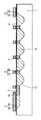
図1は、本発明の第1の実施の形態に係る高周波受動素子の外観を示す斜視図である。<First Embodiment>
FIG. 1 is a perspective view showing an appearance of a high-frequency passive device according to the first embodiment of the present invention.
図1を参照して、高周波受動素子101は、マイクロマシニング技術を用いて形成され、マイクロ波、準ミリ波およびミリ波などの高周波帯で用いられる。 Referring to FIG. 1, a high-frequency
図2〜図10は、本発明の第1の実施の形態に係る高周波受動素子の製造方法を示す断面図である。図10は、本発明の第1の実施の形態に係る高周波受動素子の図1におけるX−X断面を示す断面図である。また、図2〜図9は、本発明の第1の実施の形態に係る高周波受動素子の図1におけるX−X断面に対応している。 2-10 is sectional drawing which shows the manufacturing method of the high frequency passive element based on the 1st Embodiment of this invention. 10 is a cross-sectional view showing the XX cross section in FIG. 1 of the high-frequency passive device according to the first embodiment of the present invention. 2 to 9 correspond to the XX cross section in FIG. 1 of the high-frequency passive device according to the first embodiment of the present invention.
図1および図10を参照して、高周波受動素子101は、シリコン基板1と、第1巻き線導体2と、絶縁支持膜3と、第2巻き線導体4と、接続部5,31と、ホール6と、信号線7,33と、グランド導体8,32と、凹部9,13とを備える。 Referring to FIGS. 1 and 10, the high-frequency
入力部36は、信号線7の第1端およびグランド導体8,32の第1端で構成される。出力部37は、信号線33の第1端およびグランド導体8,32の第2端で構成される。 The
シリコン基板1は主表面S1を有し、主表面S1に凹部9が形成されている。第1巻き線導体2は、凹部9の底面に形成されている。また、第1巻き線導体2の上面は、主表面S1と略平行である。また、凹部9の底面において、第1巻き線導体2の線導体間に微小な凹部13が形成されている。
絶縁支持膜3は、凹部9の開口部および凹部13の開口部を覆うように第1巻き線導体2およびシリコン基板1の主表面S1上に平坦に形成されている。
第2巻き線導体4は、絶縁支持膜3上に形成されている。接続部31は、入力部36付近において絶縁支持膜3を貫通することにより信号線7と第1巻き線導体2とを電気的に接続する。 The second winding
接続部5は、シリコン基板1の中央部付近において絶縁支持膜3を貫通することにより第1巻き線導体2と第2巻き線導体4とを電気的に接続する。このような構成により、第1巻き線導体2および第2巻き線導体4が全体で1つの線導体になる、すなわち2重巻き線導体となる。 The
また、第1巻き線導体2および第2巻き線導体4の各々は、シリコン基板1の厚み方向において互いに完全に重なる線導体を含んでいる。 Further, each of the
ホール6は、後述する犠牲材料14を除去するために設けられている。
次に、本発明の第1の実施の形態に係る高周波受動素子の製造方法について説明する。The
Next, a method for manufacturing the high-frequency passive element according to the first embodiment of the present invention will be described.
図2を参照して、まず、シリコン基板1にウェットエッチングを施すことにより、凹部9を設ける。 Referring to FIG. 2, first,
図3を参照して、次に、たとえば金をスパッタすることによりメッキ用のシード層10を形成する。そして、メッキ用のレジスト11を塗布することによってパターニングを行なった後、金メッキなどにより厚膜導体12を形成する。なお、本発明の実施の形態において、「厚膜」とは、たとえば数μm以上の厚さを有する膜を意味する。 Referring to FIG. 3, next, plating
図4を参照して、次に、メッキ用のレジスト11を除去し、エッチバックによりシード層10をエッチングする。このとき、厚膜導体12もエッチングされ、その結果残る厚膜導体12と、その厚膜導体12の下に残っているシード層10とが第1巻き線導体2になる。第1巻き線導体2の高さは凹部9の深さと同じになるように形成する、すなわち第1巻き線導体2の上面が主表面S1と略平行になるように形成する。第1巻き線導体2は、たとえば約5μm以上の厚膜に形成する。 Referring to FIG. 4, next, plating resist 11 is removed, and
図5を参照して、次に、凹部9の底面において、第1巻き線導体2の線導体間に凹部13をウェットエチングにより形成する。 With reference to FIG. 5, next, on the bottom surface of the
図6を参照して、次に、たとえばレジストなどの犠牲材料14を凹部9および凹部13に充填する。そして、犠牲材料14の上面と基板1の上面とが一致するように犠牲材料14を研磨する。 Referring to FIG. 6, next,
図7を参照して、次に、凹部9の開口部および凹部13の開口部を覆うようにたとえば約1μm厚さを有する窒化膜からなる平坦な絶縁支持膜3を第1巻き線導体2およびシリコン基板1の主表面S1上に設ける。そして、絶縁支持膜3を貫通することにより、信号線7と第1巻き線導体2とを電気的に接続するための接続部31をドライエッチングにより形成する。また、絶縁支持膜3を貫通することにより、第1巻き線導体2と第2巻き線導体4とを電気的に接続するための接続部5をドライエッチングにより形成する。 Referring to FIG. 7, next, flat insulating
図8を参照して、次に、たとえば金をスパッタし、メッキ用のシード層20を形成し、メッキ用のレジスト21を塗布し、パターニングした後、金メッキなどにより厚膜導体22を形成する。 Referring to FIG. 8, next, for example, gold is sputtered to form a
図9を参照して、次に、メッキ用のレジスト21を除去し、エッチバックによりシード層20をエッチングする。このとき、厚膜導体22もエッチングされ、その結果残る厚膜導体22と、厚膜導体22の下に残っているシード層20とが第2巻き線導体4および信号線7,33になる。なお、第2巻き線導体4の厚みは、約5μm以上であることが好ましい。 Referring to FIG. 9, next, resist 21 for plating is removed, and
図10を参照して、次に、犠牲材料14を除去するためのホール6をドライエッチングにより形成する。最後に、ウェットエッチングを実施することでホール6を介して犠牲材料14を除去することにより、空気層に囲まれた2重の巻き線導体からなるインダクタが得られる。 Referring to FIG. 10, next, a
次に、本発明の第1の実施の形態に係る高周波受動素子の動作について説明する。
入力部36に高周波信号が入力されると、高周波信号は、巻き線導体2および巻き線導体4を通って出力部37から出力される。Next, the operation of the high-frequency passive element according to the first embodiment of the present invention will be described.
When a high frequency signal is input to the
これにより、高周波信号すなわち高周波電流が略円形の渦巻き形状の経路を流れる。すなわち、第1巻き線導体2は渦巻き形状であるため、第1巻き線導体2において隣り合う線導体に流れる高周波電流の向きは同じである。同様に、第2巻き線導体4は渦巻き形状であるため、第2巻き線導体4において隣り合う線導体に流れる高周波電流の向きは同じである。 Thereby, a high-frequency signal, that is, a high-frequency current flows through a substantially circular spiral path. That is, since the
また、第1巻き線導体2および第2巻き線導体4は、シリコン基板1の厚み方向において重なる線導体を含み、かつ重なった線導体における電流の向きが同じになるように形成されている。 Further, the first winding
このような構成により、第1巻き線導体2および第2巻き線導体4は、1個のインダクタとして働くことから、第1巻き線導体2および第2巻き線導体4の各々の自己インダクタンスに加えて、第1巻き線導体2および第2巻き線導体4による相互インダクタンスがさらに追加される。 With such a configuration, the first winding
また、第1巻き線導体2および第2巻き線導体4は、シリコン基板1の厚み方向において互いに完全に重なる線導体を含む。このような構成により、完全に重なった線導体における相互インダクタンスは最大になるため、単位面積あたりで高いインダクタンスを得ることができる。 The first winding
第1巻き線導体2および第2巻き線導体4において互いに重なる線導体の長さを変更することにより、相互インダクタンスを調整することができる。また、シリコン基板1の厚み方向において重なっている第1巻き線導体2における線導体および第2巻き線導体4における線導体の重なり度合いを変更することにより、相互インダクタンスを調整することができる。 The mutual inductance can be adjusted by changing the lengths of the line conductors that overlap each other in the first winding
本発明の第1の実施の形態に係る高周波受動素子およびその製造方法では、第1巻き線導体2は、凹部9の底面に形成されることから厚膜化が容易である。これにより、高周波受動素子の低損失化を図ることができる。 In the high-frequency passive element and the method for manufacturing the same according to the first embodiment of the present invention, the first winding
また、図10に示す高周波受動素子101の断面で見た場合、微小な多数の凹部間に形成された第1巻き線導体2の上に絶縁支持膜3が形成されることから、絶縁支持膜3は、特許文献2記載の高周波インダクタ素子のような広い凹部の上に形成される絶縁支持膜よりも撓みにくくなるため、平坦に形成することができ、かつ機械的な強度を向上させることができる。 Further, when viewed in the cross section of the high-frequency
そして、第1巻き線導体2および第2巻き線導体4は、撓み難い絶縁支持膜3の上下に形成されることから、第1巻き線導体2および第2巻き線導体4の両方を平坦に形成することができる。このため、第1巻き線導体2と同様に第2巻き線導体4の厚膜化も容易であることから、高周波受動素子の低損失化を図ることができる。また、第1巻き線導体2および第2巻き線導体4の両方を平坦に形成することができることから、設計どおりの電気的特性を得ることができる。 And since the
さらに、絶縁支持膜3を平坦に形成することができるため、第2巻き線導体4の形成位置がフレキシブルになり、相互インダクタンスを容易に調整することができる。 Furthermore, since the insulating
また、凹部9の底面において、第1巻き線導体2の線導体間に微小な凹部13が形成されることにより、シリコン基板1を介した寄生容量すなわち第1巻き線導体2における線導体間の寄生容量を低減することができるため、高周波受動素子の低損失化を図ることができる。 Further, by forming a
また、絶縁支持膜3を介してシード層20を形成することにより、メッキによる厚膜化工程の際に熱および応力による犠牲材料上面の変形を抑制することができるため、特許文献2記載の高周波インダクタ素子のように、犠牲材料の上にシード層が形成される構成よりも第2巻き線導体4を平坦にすることができる。 Further, since the
また、本発明の第1の実施の形態に係る高周波受動素子およびその製造方法では、積層構造を有する3次元金属素子を空中に浮かぶように作製する必要がないため、略2次元の集積回路と共に集積されても実装容積が大きくなることはない。 Further, in the high-frequency passive element and the manufacturing method thereof according to the first embodiment of the present invention, it is not necessary to manufacture a three-dimensional metal element having a laminated structure so as to float in the air. Even if they are integrated, the mounting volume does not increase.
したがって、本発明の第1の実施の形態に係る高周波受動素子およびその製造方法では、絶縁膜下に形成される導体線路の厚膜化を容易にし、かつ絶縁膜を平坦に形成することにより、良好な特性を実現し、かつ小型化を図ることができる。 Therefore, in the high-frequency passive element and the manufacturing method thereof according to the first embodiment of the present invention, by facilitating the thickening of the conductor line formed under the insulating film and forming the insulating film flat, Good characteristics can be realized and downsizing can be achieved.
また、特許文献1記載の3次元金属素子およびその製造方法では、メッキ工程の反復と2重露光法とを用いることにより、3次元金属素子が積層構造を有するように作製される。さらに、低損失にするために3次元金属素子を空中に浮かぶように作製することから、作製工程が複雑となり、コストがかかる欠点がある。 Further, in the three-dimensional metal element and the manufacturing method thereof described in
しかしながら、本発明の第1の実施の形態に係る高周波受動素子およびその製造方法では、積層構造を有する3次元金属素子を空中に浮かぶように作製する必要がないため、製造コストの低減を図ることができる。 However, in the high-frequency passive element and the manufacturing method thereof according to the first embodiment of the present invention, it is not necessary to manufacture a three-dimensional metal element having a laminated structure so as to float in the air, so that the manufacturing cost can be reduced. Can do.
また、特許文献2記載の高周波インダクタ素子およびその製造方法では、基板に形成された広い凹部を犠牲層で埋め込む必要があるため、コストがかかる欠点がある。 In addition, the high-frequency inductor element described in
しかしながら、本発明の第1の実施の形態に係る高周波受動素子およびその製造方法では、凹部13を第1巻き線導体2の線導体間だけに形成する。これにより、凹部13が微小幅となるため、埋め込む犠牲材料の量を少なくすることができ、製造コストの低減を図ることができる。 However, in the high-frequency passive element and the method for manufacturing the same according to the first embodiment of the present invention, the
また、特許文献2記載の高周波インダクタ素子およびその製造方法では、レジストなどによって構成される犠牲層の上面に導体線路の厚膜化のためにシード層が形成される場合には、犠牲層とシード層との密着力が弱いためにシード層が剥がれやすくなることから、製造歩留まりが低くなる欠点がある。 Further, in the high-frequency inductor element and the manufacturing method thereof described in
しかしながら、本発明の第1の実施の形態に係る高周波受動素子およびその製造方法では、第2巻き線導体4を構成するシード層20は、絶縁支持膜3を介して形成されるため、犠牲材料の上にシード層が形成される構成よりも密着力が強くなることから剥がれにくくなる。これにより、メッキによる膜厚分布が安定するため、製造歩留まりを向上させることができる。 However, in the high-frequency passive device and the method for manufacturing the same according to the first embodiment of the present invention, the
次に、本発明の他の実施の形態について図面を用いて説明する。なお、図中同一または相当部分には同一符号を付してその説明は繰り返さない。 Next, another embodiment of the present invention will be described with reference to the drawings. In the drawings, the same or corresponding parts are denoted by the same reference numerals and description thereof will not be repeated.
<第2の実施の形態>
本実施の形態は、第1巻き線導体2および第2巻き線導体4を電気的に分離した高周波受動素子に関する。以下で説明する内容以外は第1の実施の形態に係る高周波受動素子と同様である。<Second Embodiment>
The present embodiment relates to a high-frequency passive element in which the first winding
図11は、本発明の第2の実施の形態に係る高周波受動素子の構成を示す断面図である。 FIG. 11 is a cross-sectional view showing the configuration of the high-frequency passive element according to the second embodiment of the present invention.
図11を参照して、高周波受動素子102は、本発明の第1の実施の形態に係る高周波受動素子と比べて、接続部5を備えない構成である。すなわち、絶縁支持膜3の上下に形成される第1巻き線導体2と第2巻き線導体4とが絶縁支持膜3により電気的に分離されている。 Referring to FIG. 11, the high-frequency
また、第1巻き線導体2および第2巻き線導体4は、シリコン基板1の厚み方向において重なる線導体を含み、かつ重なった線導体における電流の向きが逆になるように形成されている。 The first winding
このような構成により、入力部36に入力された高周波信号が第1巻き線導体2に流れ、電磁気誘導により第2巻き線導体4へ伝送され、そして出力部37から出力されるトランスフォーマが得られる。 With this configuration, a high-frequency signal input to the
また、本発明の第1の実施の形態に係る高周波受動素子およびその製造方法と同様に、第1巻き線導体2および第2巻き線導体の厚膜化が容易であり、また、凹部13により第1巻き線導体2における線導体間の寄生容量も小さくなることから、低損失なトランスフォーマを得ることができる。 Further, similarly to the high-frequency passive element and the manufacturing method thereof according to the first embodiment of the present invention, it is easy to increase the thickness of the first winding
その他の構成および動作は第1の実施の形態に係る高周波受動素子と同様であるため、ここでは詳細な説明を繰り返さない。したがって、本発明の第2の実施の形態に係る高周波受動素子では、絶縁膜下に形成される導体線路の厚膜化を容易にし、かつ絶縁膜を平坦に形成することにより、良好な特性を実現し、小型化を図り、製造コストを低減し、かつ高い歩留まりを実現することができる。 Since other configurations and operations are the same as those of the high-frequency passive device according to the first embodiment, detailed description thereof will not be repeated here. Therefore, in the high-frequency passive device according to the second embodiment of the present invention, it is easy to increase the thickness of the conductor line formed under the insulating film, and the insulating film is formed flat, thereby providing good characteristics. Realization, downsizing, manufacturing cost reduction, and high yield can be realized.
次に、本発明の他の実施の形態について図面を用いて説明する。なお、図中同一または相当部分には同一符号を付してその説明は繰り返さない。 Next, another embodiment of the present invention will be described with reference to the drawings. In the drawings, the same or corresponding parts are denoted by the same reference numerals and description thereof will not be repeated.
<第3の実施の形態>
本実施の形態は、第2の実施の形態に係る高周波受動素子と比べて巻き線導体を追加した高周波受動素子に関する。以下で説明する内容以外は第2の実施の形態に係る高周波受動素子と同様である。<Third Embodiment>
The present embodiment relates to a high-frequency passive element in which a winding conductor is added compared to the high-frequency passive element according to the second embodiment. The contents other than those described below are the same as those of the high-frequency passive element according to the second embodiment.
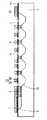
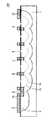
図12は、本発明の第3の実施の形態に係る高周波受動素子の外観を示す斜視図である。 FIG. 12 is a perspective view showing an appearance of a high-frequency passive device according to the third embodiment of the present invention.
図13は、本発明の第3の実施の形態に係る高周波受動素子の図12におけるXIII−XIII断面を示す断面図である。 FIG. 13 is a cross-sectional view showing the XIII-XIII cross section in FIG. 12 of the high-frequency passive device according to the third embodiment of the present invention.
図12を参照して、高周波受動素子103は、本発明の第2の実施の形態に係る高周波受動素子と比べて、さらに、第3巻き線導体15と、グランド導体34と、信号線35とを備える。 Referring to FIG. 12, the high-frequency
入力部36は、信号線7の第1端およびグランド導体8,32の第1端で構成される。出力部37は、信号線33の第1端およびグランド導体8,34の第2端で構成される。出力部38は、信号線35の第1端、グランド導体32の第2端およびグランド導体34の第1端で構成される。 The
また、第3巻き線導体15の形成は、第2巻き線導体4が形成される工程(図9)において行なわれる。すなわち、メッキ用のレジスト21を除去し、エッチバックによりシード層20をエッチングする。このとき、厚膜導体22もエッチングされ、その結果残る厚膜導体22と、厚膜導体22の下に残っているシード層20とが第2巻き線導体4、第3巻き線導体15および信号線7,33,35になる。第2巻き線導体4および第3巻き線導体15の厚みは、約5μm以上であることが好ましい。第3巻き線導体15は、第2巻き線導体4に沿うように絶縁支持膜3上に形成される、すなわち、第2巻き線導体4から離間し、かつ第2巻き線導体4の線導体間に形成される。 Further, the third winding
入力部36に入力された高周波信号は第1巻き線導体2に流れ、電磁気誘導により第2巻き線導体4および第3巻き線導体15へそれぞれ伝送され、そして、出力部37および38からそれぞれ出力される。 The high-frequency signal input to the
このような構成により、第1巻き線導体2から第2巻き線導体4へ、かつ第1巻き線導体2から第3巻き線導体15へそれぞれ特性が異なる高周波信号が電磁気誘導によって分配されるトランスフォーマが得られる。 With such a configuration, a high-frequency signal having different characteristics from the first winding
ここで、第1巻き線導体2と第2巻き線導体4との位置関係、および第1巻き線導体2と第3巻き線導体15との位置関係は、第2巻き線導体4および第3巻き線導体15へそれぞれ分配したい高周波信号の特性に応じて決定される。 Here, the positional relationship between the first winding
また、第3巻き線導体15は、第2巻き線導体4と同様の理由により厚膜化が容易であり、また、凹部13により第1巻き線導体2における線導体間の寄生容量も小さくなることから、低損失なトランスフォーマを得ることができる。 Further, the third winding
また、絶縁支持膜3を平坦に形成することができるため、第2巻き線導体4および第3巻き線導体15の形成位置がフレキシブルになり、相互インダクタンスを容易に調整することができる、すなわち、第2巻き線導体4および第3巻き線導体15へそれぞれ分配される高周波信号の特性を容易に調整することができる。 Further, since the insulating
その他の構成および動作は第2の実施の形態に係る高周波受動素子と同様であるため、ここでは詳細な説明を繰り返さない。したがって、本発明の第3の実施の形態に係る高周波受動素子では、絶縁膜下に形成される導体線路の厚膜化を容易にし、かつ絶縁膜を平坦に形成することにより、良好な特性を実現し、小型化を図り、製造コストを低減し、かつ高い歩留まりを実現することができる。 Since other configurations and operations are the same as those of the high-frequency passive device according to the second embodiment, detailed description thereof will not be repeated here. Therefore, in the high-frequency passive device according to the third embodiment of the present invention, it is easy to increase the thickness of the conductor line formed under the insulating film, and the insulating film is formed flat, thereby providing good characteristics. Realization, downsizing, manufacturing cost reduction, and high yield can be realized.
次に、本発明の他の実施の形態について図面を用いて説明する。なお、図中同一または相当部分には同一符号を付してその説明は繰り返さない。 Next, another embodiment of the present invention will be described with reference to the drawings. In the drawings, the same or corresponding parts are denoted by the same reference numerals and description thereof will not be repeated.
<第4の実施の形態>
本実施の形態は、第1の実施の形態に係る高周波受動素子と比べてさらに低損失化を図った高周波受動素子に関する。以下で説明する内容以外は第1の実施の形態に係る高周波受動素子と同様である。<Fourth embodiment>
The present embodiment relates to a high-frequency passive element that is further reduced in loss compared to the high-frequency passive element according to the first embodiment. The contents other than those described below are the same as those of the high-frequency passive device according to the first embodiment.
図14は、本発明の第4の実施の形態に係る高周波受動素子の構成を示す断面図である。図14は、本発明の第1の実施の形態に係る高周波受動素子およびその製造方法の図1におけるX−X断面に対応する位置の断面を示している。 FIG. 14 is a cross-sectional view showing the configuration of the high-frequency passive element according to the fourth embodiment of the present invention. FIG. 14 shows a cross-section at a position corresponding to the XX cross-section in FIG. 1 of the high-frequency passive device and the manufacturing method thereof according to the first embodiment of the present invention.
図14を参照して、高周波受動素子104は、本発明の第1の実施の形態に係る高周波受動素子と比べて、さらに、空気層16を備える。空気層16は、第1巻き線導体2および凹部13の下に形成される。 Referring to FIG. 14, the high-frequency
シリコン基板1の比抵抗が非常に低い場合には、本発明の第1の実施の形態に係る高周波受動素子の製造方法において犠牲材料14を除去する工程(図10)の後、図14に示すように等方性ドライエッチングを行なって第1巻き線導体2の下部および凹部13の下部を空気層16にする。このような構成により、シリコン基板1を介して生じる第1巻き線導体2の線導体間の寄生容量をさらに低減することができる。 When the specific resistance of the
その他の構成および動作は第1の実施の形態に係る高周波受動素子と同様であるため、ここでは詳細な説明を繰り返さない。したがって、本発明の第4の実施の形態に係る高周波受動素子では、絶縁膜下に形成される導体線路の厚膜化を容易にし、かつ絶縁膜を平坦に形成することにより、良好な特性を実現し、小型化を図り、製造コストを低減し、かつ高い歩留まりを実現することができる。 Since other configurations and operations are the same as those of the high-frequency passive device according to the first embodiment, detailed description thereof will not be repeated here. Therefore, in the high-frequency passive device according to the fourth embodiment of the present invention, it is easy to increase the thickness of the conductor line formed under the insulating film, and the insulating film is formed flat, thereby providing good characteristics. Realization, downsizing, manufacturing cost reduction, and high yield can be realized.
なお、本発明の第1〜第4の実施の形態に係る高周波受動素子の製造方法では、絶縁支持膜3としてたとえば窒化膜を使用したが、これに限定するものではない。フォトリソグラフィー技術によりパターニングおよびエッチングの処理を実行することができ、かつ酸化薄膜および磁性薄膜などの比較的小さい誘電損失を有する材料を絶縁支持膜3として使用する構成であってもよい。 In the high-frequency passive element manufacturing method according to the first to fourth embodiments of the present invention, for example, a nitride film is used as the insulating
また、本発明の第1〜第4の実施の形態に係る高周波受動素子の製造方法では、凹部9および13をウェットエチング法により形成したが、これに限定するものではなく、ドライエッチング法により形成してもよい。 Moreover, in the manufacturing method of the high frequency passive element according to the first to fourth embodiments of the present invention, the
また、本発明の第1〜第4の実施の形態に係る高周波受動素子の製造方法では、第1巻き線導体2、第2巻き線導体4および第3巻き線導体15の材料として金を用いたが、これに限定するものではない。金以外にもフォトリソグラフィー技術によりパターニングおよびエッチング処理を実行できる金属であれば、これら巻き線導体の材料として用いることができる。 Moreover, in the manufacturing method of the high frequency passive element which concerns on the 1st-4th embodiment of this invention, gold is used as a material of the
また、本発明の第1〜第4の実施の形態に係る高周波受動素子の製造方法では、第1巻き線導体2、第2巻き線導体4および第3巻き線導体15は略円形の渦巻き形状であるとしたが、これに限定するものではなく、たとえば多角形であってもよい。 Moreover, in the manufacturing method of the high frequency passive element which concerns on the 1st-4th embodiment of this invention, the
また、本発明の第1〜第4の実施の形態に係る高周波受動素子の製造方法では、シリコン基板を使用したが、これに限定するものではなく、基板の材質はガラスなど微細な加工が可能な材料であればよい。 Moreover, although the silicon substrate was used in the manufacturing method of the high frequency passive element according to the first to fourth embodiments of the present invention, the substrate material is not limited to this, and the substrate material can be finely processed such as glass. Any material can be used.
今回開示された実施の形態はすべての点で例示であって制限的なものではないと考えられるべきである。本発明の範囲は上記した説明ではなくて特許請求の範囲によって示され、特許請求の範囲と均等の意味および範囲内でのすべての変更が含まれることが意図される。 The embodiment disclosed this time should be considered as illustrative in all points and not restrictive. The scope of the present invention is defined by the terms of the claims, rather than the description above, and is intended to include any modifications within the scope and meaning equivalent to the terms of the claims.
1 シリコン基板、2 第1巻き線導体、3 絶縁支持膜、4 第2巻き線導体、5,31 接続部、6 ホール、7,33,35 信号線、8,32,34 グランド導体、9,13 凹部、10,20 シード層、11,21 レジスト、12,22 厚膜導体、14 犠牲材料、15 第3巻き線導体、16 空気層、36 入力部、37,38 出力部、101〜104 高周波受動素子、S1 主表面。 DESCRIPTION OF
Claims (14)
Translated fromJapanese前記第1の凹部の底面に形成され、かつ上面が前記基板の前記主表面と略平行になるように形成された第1巻き線導体と、
前記第1巻き線導体および前記基板の前記主表面上に平坦に形成された絶縁膜と、
前記絶縁膜上に形成された第2巻き線導体とを備える高周波受動素子。A substrate having a first recess formed on a main surface;
A first winding conductor formed on the bottom surface of the first recess and having an upper surface substantially parallel to the main surface of the substrate;
An insulating film formed flat on the main surface of the first winding conductor and the substrate;
A high-frequency passive element comprising: a second winding conductor formed on the insulating film.
前記絶縁膜を貫通することにより前記第1巻き線導体と前記第2巻き線導体とを電気的に接続する接続部を備え、
前記第1巻き線導体および前記第2巻き線導体は、前記基板の厚み方向において重なる線導体を含み、かつ前記重なった線導体における電流の向きが同じになるように形成された請求項1記載の高周波受動素子。The high-frequency passive element further includes:
A connecting portion for electrically connecting the first winding conductor and the second winding conductor by penetrating the insulating film;
The said 1st winding conductor and the said 2nd winding conductor are formed so that the direction of the electric current in the said overlapping line conductor may be the same including the line conductor which overlaps in the thickness direction of the said board | substrate. High frequency passive element.
前記絶縁膜上かつ前記第2巻き線導体の線導体間において前記第2巻き線導体から離間して形成された第3巻き線導体を備える請求項1記載の高周波受動素子。The high-frequency passive element further includes:
2. The high-frequency passive element according to claim 1, further comprising a third winding conductor formed on the insulating film and between the line conductors of the second winding conductor so as to be separated from the second winding conductor.
前記第1の凹部の底面に、上面が前記基板の前記主表面と略平行である第1巻き線導体を形成するステップと、
前記第1巻き線導体および前記基板の前記主表面上に平坦な絶縁膜を形成するステップと、
前記絶縁膜上に第2巻き線導体を形成するステップとを含む高周波受動素子の製造方法。Forming a first recess in the main surface of the substrate;
Forming a first wound conductor on the bottom surface of the first recess, the upper surface of which is substantially parallel to the main surface of the substrate;
Forming a flat insulating film on the main surface of the first winding conductor and the substrate;
Forming a second winding conductor on the insulating film.
前記第1の凹部の底面において、前記第1巻き線導体の線導体間に第2の凹部を形成するステップを含む請求項8記載の高周波受動素子の製造方法。The method for manufacturing the high-frequency passive device further includes:
The method for manufacturing a high-frequency passive element according to claim 8, further comprising a step of forming a second recess between the line conductors of the first winding conductor on the bottom surface of the first recess.
前記基板の厚み方向において前記第1巻き線導体が含む線導体と完全に重なる線導体を含む第2巻き線導体を形成する請求項8記載の高周波受動素子の製造方法。In the step of forming the second winding conductor,
The method of manufacturing a high-frequency passive element according to claim 8, wherein a second winding conductor including a line conductor that completely overlaps with the line conductor included in the first winding conductor is formed in the thickness direction of the substrate.
前記絶縁膜を貫通することにより前記第1巻き線導体と前記第2巻き線導体とを電気的に接続する接続部を形成するステップを含み、
前記第2巻き線導体を形成するステップにおいては、
前記基板の厚み方向において前記第1巻き線導体が含む線導体と重なる線導体を含み、かつ前記重なった線導体における電流の向きが前記第1巻き線導体の含む線導体と同じである第2巻き線導体を形成する請求項8記載の高周波受動素子の製造方法。The method for manufacturing the high-frequency passive device further includes:
Forming a connection portion that electrically connects the first winding conductor and the second winding conductor by penetrating the insulating film;
In the step of forming the second winding conductor,
A second conductor that includes a line conductor that overlaps the line conductor included in the first winding conductor in the thickness direction of the substrate, and that has a current direction that is the same as the line conductor included in the first winding conductor. The manufacturing method of the high frequency passive element of Claim 8 which forms a winding conductor.
前記第1巻き線導体と電気的に絶縁され、前記基板の厚み方向において前記第1巻き線導体が含む線導体と重なる線導体を含み、かつ前記重なった線導体における電流の向きが前記第1巻き線導体の含む線導体と逆である第2巻き線導体を形成する請求項8記載の高周波受動素子の製造方法。The method for manufacturing the high-frequency passive device further includes:
The first winding conductor includes a line conductor that is electrically insulated from the first winding conductor and overlaps the line conductor included in the first winding conductor in the thickness direction of the substrate, and the direction of the current in the overlapping line conductor is the first The manufacturing method of the high frequency passive element of Claim 8 which forms the 2nd winding conductor reverse to the line conductor which a winding conductor contains.
前記絶縁膜上かつ前記第2巻き線導体の線導体間において前記第2巻き線導体から離間した第3巻き線導体を形成するステップを含む請求項8記載の高周波受動素子の製造方法。The method for manufacturing the high-frequency passive device further includes:
9. The method of manufacturing a high-frequency passive element according to claim 8, further comprising a step of forming a third winding conductor spaced from the second winding conductor on the insulating film and between the line conductors of the second winding conductor.
前記基板において、前記第1巻き線導体の下部の領域を含む空気層を形成するステップを含む請求項8記載の高周波受動素子の製造方法。The method for manufacturing the high-frequency passive device further includes:
The method for manufacturing a high-frequency passive element according to claim 8, further comprising: forming an air layer including a lower region of the first winding conductor on the substrate.
Priority Applications (1)
| Application Number | Priority Date | Filing Date | Title |
|---|---|---|---|
| JP2007232862AJP4815623B2 (en) | 2007-09-07 | 2007-09-07 | High frequency passive device and method for manufacturing the same |
Applications Claiming Priority (1)
| Application Number | Priority Date | Filing Date | Title |
|---|---|---|---|
| JP2007232862AJP4815623B2 (en) | 2007-09-07 | 2007-09-07 | High frequency passive device and method for manufacturing the same |
Publications (2)
| Publication Number | Publication Date |
|---|---|
| JP2009065042A JP2009065042A (en) | 2009-03-26 |
| JP4815623B2true JP4815623B2 (en) | 2011-11-16 |
Family
ID=40559347
Family Applications (1)
| Application Number | Title | Priority Date | Filing Date |
|---|---|---|---|
| JP2007232862AExpired - Fee RelatedJP4815623B2 (en) | 2007-09-07 | 2007-09-07 | High frequency passive device and method for manufacturing the same |
Country Status (1)
| Country | Link |
|---|---|
| JP (1) | JP4815623B2 (en) |
Families Citing this family (6)
| Publication number | Priority date | Publication date | Assignee | Title |
|---|---|---|---|---|
| JP6405742B2 (en)* | 2014-06-26 | 2018-10-17 | 富士通株式会社 | Coil component and method of manufacturing coil component |
| US20160284461A1 (en)* | 2015-03-28 | 2016-09-29 | Intel IP Corporation | Tuning inductance ratio of a passive device |
| JP7032214B2 (en)* | 2018-04-02 | 2022-03-08 | 株式会社村田製作所 | Laminated coil parts |
| CN109887707B (en)* | 2017-11-27 | 2022-04-12 | 株式会社村田制作所 | Laminated coil components |
| JP6954216B2 (en) | 2018-04-02 | 2021-10-27 | 株式会社村田製作所 | Laminated coil parts |
| JP6954217B2 (en) | 2018-04-02 | 2021-10-27 | 株式会社村田製作所 | Laminated coil parts |
Family Cites Families (12)
| Publication number | Priority date | Publication date | Assignee | Title |
|---|---|---|---|---|
| JPS5246787A (en)* | 1975-10-11 | 1977-04-13 | Hitachi Ltd | Coil for integrated circuit and process for production of same |
| DE4331798B4 (en)* | 1993-09-18 | 2004-08-26 | Robert Bosch Gmbh | Process for the production of micromechanical components |
| US5596226A (en)* | 1994-09-06 | 1997-01-21 | International Business Machines Corporation | Semiconductor chip having a chip metal layer and a transfer metal and corresponding electronic module |
| JPH08222438A (en)* | 1995-02-16 | 1996-08-30 | Matsushita Electric Works Ltd | Inductance and transformer |
| US5825092A (en)* | 1996-05-20 | 1998-10-20 | Harris Corporation | Integrated circuit with an air bridge having a lid |
| US6492705B1 (en)* | 1996-06-04 | 2002-12-10 | Intersil Corporation | Integrated circuit air bridge structures and methods of fabricating same |
| EP1130631A1 (en)* | 2000-02-29 | 2001-09-05 | STMicroelectronics S.r.l. | Process for forming a buried cavity in a semiconductor material wafer |
| KR100382765B1 (en)* | 2001-06-15 | 2003-05-09 | 삼성전자주식회사 | Passive devices and modules for transceiver and manufacturing method thereof |
| JP4159378B2 (en)* | 2002-04-25 | 2008-10-01 | 三菱電機株式会社 | High frequency device and manufacturing method thereof |
| JP2005244084A (en)* | 2004-02-27 | 2005-09-08 | Mitsubishi Electric Corp | Spiral high frequency coil and manufacturing method thereof |
| KR100548388B1 (en)* | 2004-07-20 | 2006-02-02 | 삼성전자주식회사 | Low Loss Inductor Device and Manufacturing Method Thereof |
| JP2007165343A (en)* | 2005-12-09 | 2007-06-28 | Nec Electronics Corp | Thin film transformer and manufacturing method thereof |
- 2007
- 2007-09-07JPJP2007232862Apatent/JP4815623B2/ennot_activeExpired - Fee Related
Also Published As
| Publication number | Publication date |
|---|---|
| JP2009065042A (en) | 2009-03-26 |
Similar Documents
| Publication | Publication Date | Title |
|---|---|---|
| US7408434B2 (en) | Inductor embedded in substrate, manufacturing method thereof, micro device package, and manufacturing method of cap for micro device package | |
| JP4815623B2 (en) | High frequency passive device and method for manufacturing the same | |
| US8826514B2 (en) | Microfabricated inductors with through-wafer vias | |
| JP4159378B2 (en) | High frequency device and manufacturing method thereof | |
| SE534510C2 (en) | Functional encapsulation | |
| JP2000353617A (en) | Micro-elements of the type such as micro-inductors and micro-transformers and methods of manufacturing such micro-elements | |
| KR20060136202A (en) | Inductor and method for manufacturing thereof, micro device package and method for manufacturing cap of the micro device package | |
| JP2004001186A (en) | MEMS device and manufacturing method thereof | |
| CN105742251A (en) | Structure with inductor and metal-insulator-metal capacitor | |
| US6292084B1 (en) | Fine inductor having 3-dimensional coil structure and method for producing the same | |
| KR100469248B1 (en) | MicroInductor for Wireless Communication Module | |
| CN106531882B (en) | Electromagnetic impedance sensing element and manufacturing method thereof | |
| JP2009277617A (en) | Fine electronic mechanical switch and method of manufacturing the same | |
| CN111162050B (en) | A micro-coaxial bonding interface | |
| JP5676423B2 (en) | Isolator and semiconductor device | |
| CN102005439B (en) | High frequency device | |
| JP5621616B2 (en) | MEMS switch and manufacturing method thereof | |
| US6621139B2 (en) | Method for fabricating a tunable, 3-dimensional solenoid and device fabricated | |
| JP2008166476A (en) | Thin film transformer and manufacturing method thereof | |
| US6677659B2 (en) | Method for fabricating 3-dimensional solenoid and device fabricated | |
| CN113540915A (en) | Micro-coaxial radio frequency transmission line and GSG (ground satellite System) adapter thereof | |
| JP2005303778A (en) | Transmission line and manufacturing method thereof | |
| JP2006339197A (en) | High frequency inductor element | |
| CN106531881B (en) | Electromagnetic impedance sensing element and manufacturing method thereof | |
| JP4541718B2 (en) | High frequency integrated circuit and manufacturing method thereof |
Legal Events
| Date | Code | Title | Description |
|---|---|---|---|
| A621 | Written request for application examination | Free format text:JAPANESE INTERMEDIATE CODE: A621 Effective date:20091225 | |
| A977 | Report on retrieval | Free format text:JAPANESE INTERMEDIATE CODE: A971007 Effective date:20110629 | |
| TRDD | Decision of grant or rejection written | ||
| A01 | Written decision to grant a patent or to grant a registration (utility model) | Free format text:JAPANESE INTERMEDIATE CODE: A01 Effective date:20110802 | |
| A01 | Written decision to grant a patent or to grant a registration (utility model) | Free format text:JAPANESE INTERMEDIATE CODE: A01 | |
| A61 | First payment of annual fees (during grant procedure) | Free format text:JAPANESE INTERMEDIATE CODE: A61 Effective date:20110809 | |
| FPAY | Renewal fee payment (event date is renewal date of database) | Free format text:PAYMENT UNTIL: 20140909 Year of fee payment:3 | |
| R150 | Certificate of patent or registration of utility model | Free format text:JAPANESE INTERMEDIATE CODE: R150 | |
| LAPS | Cancellation because of no payment of annual fees |