JP4814498B2 - Manufacturing method of semiconductor substrate - Google Patents
Manufacturing method of semiconductor substrateDownload PDFInfo
- Publication number
- JP4814498B2 JP4814498B2JP2004181527AJP2004181527AJP4814498B2JP 4814498 B2JP4814498 B2JP 4814498B2JP 2004181527 AJP2004181527 AJP 2004181527AJP 2004181527 AJP2004181527 AJP 2004181527AJP 4814498 B2JP4814498 B2JP 4814498B2
- Authority
- JP
- Japan
- Prior art keywords
- substrate
- layer
- peeling
- diffusion
- semiconductor device
- Prior art date
- Legal status (The legal status is an assumption and is not a legal conclusion. Google has not performed a legal analysis and makes no representation as to the accuracy of the status listed.)
- Expired - Fee Related
Links
Images


Classifications
- H—ELECTRICITY
- H10—SEMICONDUCTOR DEVICES; ELECTRIC SOLID-STATE DEVICES NOT OTHERWISE PROVIDED FOR
- H10D—INORGANIC ELECTRIC SEMICONDUCTOR DEVICES
- H10D86/00—Integrated devices formed in or on insulating or conducting substrates, e.g. formed in silicon-on-insulator [SOI] substrates or on stainless steel or glass substrates
- H—ELECTRICITY
- H01—ELECTRIC ELEMENTS
- H01L—SEMICONDUCTOR DEVICES NOT COVERED BY CLASS H10
- H01L21/00—Processes or apparatus adapted for the manufacture or treatment of semiconductor or solid state devices or of parts thereof
- H01L21/67—Apparatus specially adapted for handling semiconductor or electric solid state devices during manufacture or treatment thereof; Apparatus specially adapted for handling wafers during manufacture or treatment of semiconductor or electric solid state devices or components ; Apparatus not specifically provided for elsewhere
- H01L21/683—Apparatus specially adapted for handling semiconductor or electric solid state devices during manufacture or treatment thereof; Apparatus specially adapted for handling wafers during manufacture or treatment of semiconductor or electric solid state devices or components ; Apparatus not specifically provided for elsewhere for supporting or gripping
- H01L21/6835—Apparatus specially adapted for handling semiconductor or electric solid state devices during manufacture or treatment thereof; Apparatus specially adapted for handling wafers during manufacture or treatment of semiconductor or electric solid state devices or components ; Apparatus not specifically provided for elsewhere for supporting or gripping using temporarily an auxiliary support
- H—ELECTRICITY
- H01—ELECTRIC ELEMENTS
- H01L—SEMICONDUCTOR DEVICES NOT COVERED BY CLASS H10
- H01L21/00—Processes or apparatus adapted for the manufacture or treatment of semiconductor or solid state devices or of parts thereof
- H01L21/02—Manufacture or treatment of semiconductor devices or of parts thereof
- H01L21/04—Manufacture or treatment of semiconductor devices or of parts thereof the devices having potential barriers, e.g. a PN junction, depletion layer or carrier concentration layer
- H01L21/18—Manufacture or treatment of semiconductor devices or of parts thereof the devices having potential barriers, e.g. a PN junction, depletion layer or carrier concentration layer the devices having semiconductor bodies comprising elements of Group IV of the Periodic Table or AIIIBV compounds with or without impurities, e.g. doping materials
- H—ELECTRICITY
- H01—ELECTRIC ELEMENTS
- H01L—SEMICONDUCTOR DEVICES NOT COVERED BY CLASS H10
- H01L24/00—Arrangements for connecting or disconnecting semiconductor or solid-state bodies; Methods or apparatus related thereto
- H01L24/93—Batch processes
- H01L24/95—Batch processes at chip-level, i.e. with connecting carried out on a plurality of singulated devices, i.e. on diced chips
- H01L24/97—Batch processes at chip-level, i.e. with connecting carried out on a plurality of singulated devices, i.e. on diced chips the devices being connected to a common substrate, e.g. interposer, said common substrate being separable into individual assemblies after connecting
- H—ELECTRICITY
- H01—ELECTRIC ELEMENTS
- H01L—SEMICONDUCTOR DEVICES NOT COVERED BY CLASS H10
- H01L2221/00—Processes or apparatus adapted for the manufacture or treatment of semiconductor or solid state devices or of parts thereof covered by H01L21/00
- H01L2221/67—Apparatus for handling semiconductor or electric solid state devices during manufacture or treatment thereof; Apparatus for handling wafers during manufacture or treatment of semiconductor or electric solid state devices or components; Apparatus not specifically provided for elsewhere
- H01L2221/683—Apparatus for handling semiconductor or electric solid state devices during manufacture or treatment thereof; Apparatus for handling wafers during manufacture or treatment of semiconductor or electric solid state devices or components; Apparatus not specifically provided for elsewhere for supporting or gripping
- H01L2221/68304—Apparatus for handling semiconductor or electric solid state devices during manufacture or treatment thereof; Apparatus for handling wafers during manufacture or treatment of semiconductor or electric solid state devices or components; Apparatus not specifically provided for elsewhere for supporting or gripping using temporarily an auxiliary support
- H01L2221/68363—Apparatus for handling semiconductor or electric solid state devices during manufacture or treatment thereof; Apparatus for handling wafers during manufacture or treatment of semiconductor or electric solid state devices or components; Apparatus not specifically provided for elsewhere for supporting or gripping using temporarily an auxiliary support used in a transfer process involving transfer directly from an origin substrate to a target substrate without use of an intermediate handle substrate
- H—ELECTRICITY
- H01—ELECTRIC ELEMENTS
- H01L—SEMICONDUCTOR DEVICES NOT COVERED BY CLASS H10
- H01L2924/00—Indexing scheme for arrangements or methods for connecting or disconnecting semiconductor or solid-state bodies as covered by H01L24/00
- H01L2924/01—Chemical elements
- H01L2924/01005—Boron [B]
- H—ELECTRICITY
- H01—ELECTRIC ELEMENTS
- H01L—SEMICONDUCTOR DEVICES NOT COVERED BY CLASS H10
- H01L2924/00—Indexing scheme for arrangements or methods for connecting or disconnecting semiconductor or solid-state bodies as covered by H01L24/00
- H01L2924/01—Chemical elements
- H01L2924/01006—Carbon [C]
- H—ELECTRICITY
- H01—ELECTRIC ELEMENTS
- H01L—SEMICONDUCTOR DEVICES NOT COVERED BY CLASS H10
- H01L2924/00—Indexing scheme for arrangements or methods for connecting or disconnecting semiconductor or solid-state bodies as covered by H01L24/00
- H01L2924/01—Chemical elements
- H01L2924/0101—Neon [Ne]
- H—ELECTRICITY
- H01—ELECTRIC ELEMENTS
- H01L—SEMICONDUCTOR DEVICES NOT COVERED BY CLASS H10
- H01L2924/00—Indexing scheme for arrangements or methods for connecting or disconnecting semiconductor or solid-state bodies as covered by H01L24/00
- H01L2924/01—Chemical elements
- H01L2924/01013—Aluminum [Al]
- H—ELECTRICITY
- H01—ELECTRIC ELEMENTS
- H01L—SEMICONDUCTOR DEVICES NOT COVERED BY CLASS H10
- H01L2924/00—Indexing scheme for arrangements or methods for connecting or disconnecting semiconductor or solid-state bodies as covered by H01L24/00
- H01L2924/01—Chemical elements
- H01L2924/01015—Phosphorus [P]
- H—ELECTRICITY
- H01—ELECTRIC ELEMENTS
- H01L—SEMICONDUCTOR DEVICES NOT COVERED BY CLASS H10
- H01L2924/00—Indexing scheme for arrangements or methods for connecting or disconnecting semiconductor or solid-state bodies as covered by H01L24/00
- H01L2924/01—Chemical elements
- H01L2924/01018—Argon [Ar]
- H—ELECTRICITY
- H01—ELECTRIC ELEMENTS
- H01L—SEMICONDUCTOR DEVICES NOT COVERED BY CLASS H10
- H01L2924/00—Indexing scheme for arrangements or methods for connecting or disconnecting semiconductor or solid-state bodies as covered by H01L24/00
- H01L2924/01—Chemical elements
- H01L2924/01019—Potassium [K]
- H—ELECTRICITY
- H01—ELECTRIC ELEMENTS
- H01L—SEMICONDUCTOR DEVICES NOT COVERED BY CLASS H10
- H01L2924/00—Indexing scheme for arrangements or methods for connecting or disconnecting semiconductor or solid-state bodies as covered by H01L24/00
- H01L2924/01—Chemical elements
- H01L2924/01033—Arsenic [As]
- H—ELECTRICITY
- H01—ELECTRIC ELEMENTS
- H01L—SEMICONDUCTOR DEVICES NOT COVERED BY CLASS H10
- H01L2924/00—Indexing scheme for arrangements or methods for connecting or disconnecting semiconductor or solid-state bodies as covered by H01L24/00
- H01L2924/01—Chemical elements
- H01L2924/01054—Xenon [Xe]
- H—ELECTRICITY
- H01—ELECTRIC ELEMENTS
- H01L—SEMICONDUCTOR DEVICES NOT COVERED BY CLASS H10
- H01L2924/00—Indexing scheme for arrangements or methods for connecting or disconnecting semiconductor or solid-state bodies as covered by H01L24/00
- H01L2924/01—Chemical elements
- H01L2924/01057—Lanthanum [La]
- H—ELECTRICITY
- H01—ELECTRIC ELEMENTS
- H01L—SEMICONDUCTOR DEVICES NOT COVERED BY CLASS H10
- H01L2924/00—Indexing scheme for arrangements or methods for connecting or disconnecting semiconductor or solid-state bodies as covered by H01L24/00
- H01L2924/01—Chemical elements
- H01L2924/01073—Tantalum [Ta]
- H—ELECTRICITY
- H01—ELECTRIC ELEMENTS
- H01L—SEMICONDUCTOR DEVICES NOT COVERED BY CLASS H10
- H01L2924/00—Indexing scheme for arrangements or methods for connecting or disconnecting semiconductor or solid-state bodies as covered by H01L24/00
- H01L2924/01—Chemical elements
- H01L2924/01074—Tungsten [W]
- H—ELECTRICITY
- H01—ELECTRIC ELEMENTS
- H01L—SEMICONDUCTOR DEVICES NOT COVERED BY CLASS H10
- H01L2924/00—Indexing scheme for arrangements or methods for connecting or disconnecting semiconductor or solid-state bodies as covered by H01L24/00
- H01L2924/049—Nitrides composed of metals from groups of the periodic table
- H01L2924/0495—5th Group
- H01L2924/04953—TaN
- H—ELECTRICITY
- H01—ELECTRIC ELEMENTS
- H01L—SEMICONDUCTOR DEVICES NOT COVERED BY CLASS H10
- H01L2924/00—Indexing scheme for arrangements or methods for connecting or disconnecting semiconductor or solid-state bodies as covered by H01L24/00
- H01L2924/10—Details of semiconductor or other solid state devices to be connected
- H01L2924/11—Device type
- H01L2924/12—Passive devices, e.g. 2 terminal devices
- H01L2924/1204—Optical Diode
- H01L2924/12042—LASER
- H—ELECTRICITY
- H01—ELECTRIC ELEMENTS
- H01L—SEMICONDUCTOR DEVICES NOT COVERED BY CLASS H10
- H01L2924/00—Indexing scheme for arrangements or methods for connecting or disconnecting semiconductor or solid-state bodies as covered by H01L24/00
- H01L2924/10—Details of semiconductor or other solid state devices to be connected
- H01L2924/11—Device type
- H01L2924/13—Discrete devices, e.g. 3 terminal devices
- H01L2924/1301—Thyristor
- H—ELECTRICITY
- H01—ELECTRIC ELEMENTS
- H01L—SEMICONDUCTOR DEVICES NOT COVERED BY CLASS H10
- H01L2924/00—Indexing scheme for arrangements or methods for connecting or disconnecting semiconductor or solid-state bodies as covered by H01L24/00
- H01L2924/10—Details of semiconductor or other solid state devices to be connected
- H01L2924/11—Device type
- H01L2924/13—Discrete devices, e.g. 3 terminal devices
- H01L2924/1304—Transistor
- H01L2924/1305—Bipolar Junction Transistor [BJT]
- H—ELECTRICITY
- H01—ELECTRIC ELEMENTS
- H01L—SEMICONDUCTOR DEVICES NOT COVERED BY CLASS H10
- H01L2924/00—Indexing scheme for arrangements or methods for connecting or disconnecting semiconductor or solid-state bodies as covered by H01L24/00
- H01L2924/10—Details of semiconductor or other solid state devices to be connected
- H01L2924/11—Device type
- H01L2924/13—Discrete devices, e.g. 3 terminal devices
- H01L2924/1304—Transistor
- H01L2924/1306—Field-effect transistor [FET]
- H01L2924/13091—Metal-Oxide-Semiconductor Field-Effect Transistor [MOSFET]
- H—ELECTRICITY
- H01—ELECTRIC ELEMENTS
- H01L—SEMICONDUCTOR DEVICES NOT COVERED BY CLASS H10
- H01L2924/00—Indexing scheme for arrangements or methods for connecting or disconnecting semiconductor or solid-state bodies as covered by H01L24/00
- H01L2924/30—Technical effects
- H01L2924/301—Electrical effects
- H01L2924/30105—Capacitance
Landscapes
- Engineering & Computer Science (AREA)
- Computer Hardware Design (AREA)
- Microelectronics & Electronic Packaging (AREA)
- Power Engineering (AREA)
- Physics & Mathematics (AREA)
- Condensed Matter Physics & Semiconductors (AREA)
- General Physics & Mathematics (AREA)
- Manufacturing & Machinery (AREA)
- Thin Film Transistor (AREA)
- Element Separation (AREA)
- Electrodes Of Semiconductors (AREA)
- Recrystallisation Techniques (AREA)
Description
Translated fromJapanese本発明は、半導体基板の製造方法に関するものである。The present invention relatesto a semiconductor substrate manufacturinghow.
従来より、絶縁層の表面に単結晶のシリコン層が形成されたシリコン基板であるSOI(Silicon On Insulator)基板が知られている。SOI基板にトランジスタ等のデバイスを形成することにより、寄生容量を低減すると共に絶縁抵抗を高くすることができる。すなわち、デバイスの高集積化や高性能化を図ることができる。上記絶縁層は、例えばシリコン酸化膜(SiO2)により形成されている。2. Description of the Related Art Conventionally, an SOI (Silicon On Insulator) substrate is known which is a silicon substrate in which a single crystal silicon layer is formed on the surface of an insulating layer. By forming a device such as a transistor on an SOI substrate, parasitic capacitance can be reduced and insulation resistance can be increased. That is, higher integration and higher performance of the device can be achieved. The insulating layer is formed of, for example, a silicon oxide film (SiO2 ).
上記SOI基板は、デバイスの動作速度を高めると共に寄生容量をさらに低減するために、単結晶シリコン層の膜厚を薄く形成することが望ましい。そこで、従来より、一組の基板を貼り合わせてSOI基板を作製する方法が知られている(例えば、非特許文献1参照)。 In order to increase the operation speed of the device and further reduce the parasitic capacitance, the SOI substrate is desirably formed with a thin single crystal silicon layer. Thus, conventionally, a method for manufacturing an SOI substrate by bonding a set of substrates is known (see, for example, Non-Patent Document 1).
ここで、上記貼り合わせによるSOI基板の作製方法について、図35〜図38を参照して説明する。なお、SOI層の薄膜化の方法は、機械研磨や化学ポリッシングやポーラスシリコンを利用した手法など種々あるが、ここでは、水素注入による方法について示す。まず、図35に示すように、第1の基板であるシリコンウェハ101の表面を酸化処理することにより、絶縁層である酸化シリコン(SiO2)層102を形成する。次に、図36に示すように、酸化シリコン(SiO2)層102を介してシリコンウェハ101中に水素イオンを注入する。このことにより、シリコンウェハ101の所定の深さ位置に剥離層104を形成する。続いて、RCA洗浄等の基板表面洗浄処理を行った後、図37に示すように、上記酸化シリコン層102の表面に第2の基板である例えばガラス基板103を貼り付ける。その後、熱処理を行うことにより、剥離層104にマイクロクラックが形成されるため、図38に示すように、シリコンウェハ101の一部を上記剥離104に沿って分離する。こうして、シリコンウェハ101を薄膜化して形成する。なお、分離後、必要に応じて研磨、エッチング等の種々の手法によって所望の膜厚に薄膜化し、また、熱処理等により水素注入によって生成される結晶欠陥修復やシリコン表面の平滑化等を行う。Here, a method for manufacturing an SOI substrate by the above bonding will be described with reference to FIGS. Note that there are various methods for thinning the SOI layer, such as mechanical polishing, chemical polishing, and methods using porous silicon. Here, a method using hydrogen injection is described. First, as shown in FIG. 35, the surface of a
以上のようにして、ガラス基板(第2の基板)103の表面に酸化シリコン層102が形成されると共に、酸化シリコン層102の表面にシリコンウェハ101の一部が薄く形成されたSOI基板が作製される。 As described above, an SOI substrate in which the
また、上記SOI基板作製方法において、水素と同時にホウ素をシリコンウェハ101に注入することも知られている(例えば、非特許文献2参照)。これは、剥離層104に沿って分離させるための熱処理温度を低減させることを目的として水素とホウ素を同時に注入するものである。
しかし、上記従来のSOI基板作製方法では、作製されたSOI基板にトランジスタ等の半導体デバイス部を形成すると、シリコンウェハの一部を剥離するために導入された水素が直接的あるいは間接的に関与し、結果としてN型不純物のような働きをしてしまう。その結果、半導体デバイス部に対し、しきい値電圧シフト等の悪影響を及ぼしてしまうという問題がある。 However, in the above conventional SOI substrate manufacturing method, when a semiconductor device portion such as a transistor is formed on the manufactured SOI substrate, hydrogen introduced to peel off a part of the silicon wafer is directly or indirectly involved. As a result, it works like an N-type impurity. As a result, there is a problem in that the semiconductor device portion is adversely affected such as a threshold voltage shift.
そこで、上記SOI基板を加熱することによって水素を除去することが考えられる。ところが、SOI基板から水素を完全に除去するためには、約800℃以上もの高温で加熱処理する必要がある。さらに、そのような高温環境下では、半導体デバイス部自体の不純物特性が変化してしまうため、実際には、半導体デバイス部が形成されたSOI基板から水素を除去することはできない。また、第2の基板は800℃以上もの高温に晒されることになるため、材料選択の幅が狭まり、例えば軟化温度が500〜700℃程度のガラスなどを使用することができなくなってしまう。 Therefore, it is conceivable to remove hydrogen by heating the SOI substrate. However, in order to completely remove hydrogen from the SOI substrate, it is necessary to perform heat treatment at a high temperature of about 800 ° C. or higher. Further, under such a high temperature environment, the impurity characteristics of the semiconductor device part itself change, so that in reality, hydrogen cannot be removed from the SOI substrate on which the semiconductor device part is formed. Further, since the second substrate is exposed to a high temperature of 800 ° C. or higher, the range of material selection is narrowed, and for example, glass having a softening temperature of about 500 to 700 ° C. cannot be used.
本発明は、斯かる諸点に鑑みてなされたものであり、その目的とするところは、基板に対し剥離層を形成して該基板の一部を剥離する手法を用いて製造する半導体基板について、基板に後に形成される或いは既に形成された半導体デバイス部が、剥離用物質の拡散によって受ける悪影響を排除することにある。 The present invention has been made in view of such various points, and the object of the present invention is to provide a semiconductor substrate manufactured using a technique of forming a release layer on a substrate and peeling a part of the substrate. An object of the present invention is to eliminate the adverse effect that a semiconductor device portion formed later or already formed on a substrate receives due to diffusion of a peeling material.
上記の目的を達成するために、この発明では、拡散抑止層を形成することにより、半導体層の一部を分割除去するための剥離用物質を、半導体デバイス部が形成される領域へ移動させないようにした。 In order to achieve the above object, according to the present invention, by forming a diffusion suppression layer, a release substance for dividing and removing a part of the semiconductor layer is not moved to a region where the semiconductor device portion is formed. I made it.
具体的には、本発明に係る半導体基板の製造方法は、基板の一部を剥離するための剥離用物質を前記基板に導入することにより、該基板の内部に剥離層を形成する工程と、前記基板の一方の表面側に半導体デバイス部の少なくとも一部を形成する工程とを含む半導体基板製造方法であって、前記剥離層を形成する前に行われ、前記剥離層が形成される領域と前記半導体デバイス部の少なくとも一部が形成される領域との間に前記剥離用物質の透過拡散を抑止する拡散抑止層を形成する工程を有し、前記拡散抑止層を形成する工程では、前記剥離用物質の拡散を抑止する拡散抑止用物質を前記基板の内部に導入することによって該基板の内部に前記拡散抑止層を形成することを特徴とする。 Specifically, the method of manufacturing a semiconductor substrate according to the present invention includes a step of forming a release layer in the substrate by introducing a release material for peeling a part of the substrate into the substrate, Forming at least a part of a semiconductor device portion on one surface side of the substrate, the method being performed before forming the release layer, and a region where the release layer is formed, And a step of forming a diffusion suppression layer that suppresses permeation diffusion of the peeling material between the region where at least a part of the semiconductor device portion is formed, and in the step of forming the diffusion suppression layer, the peeling The diffusion inhibiting layer is formed inside the substrate by introducing a diffusion inhibiting material that inhibits the diffusion of the substance into the substrate.
さらに、前記剥離層に沿って前記基板の一部を剥離する工程を有し、前記基板は、前記剥離層に沿って一部が剥離される前に、前記半導体デバイス部の少なくとも一部が形成されてもよい。 Furthermore, the method includes a step of peeling a part of the substrate along the peeling layer, and the substrate forms at least a part of the semiconductor device portion before the part is peeled along the peeling layer. May be.
また、前記剥離層に沿って前記基板の一部を剥離する工程と、一部が剥離された前記基板から前記剥離層及び前記拡散抑止層を除去する工程とを有し、前記剥離層及び前記拡散抑止層を前記基板から除去した後に、前記半導体デバイス部の少なくとも一部を形成するようにしてもよい。 A step of peeling a part of the substrate along the peeling layer; and a step of removing the peeling layer and the diffusion suppressing layer from the substrate partially peeled, the peeling layer and the After removing the diffusion suppressing layer from the substrate, at least a part of the semiconductor device portion may be formed.
また、本発明に係る半導体基板の製造方法は、基板の一部を剥離するための剥離用物質を前記基板に導入することにより、該基板の内部に剥離層を形成する工程と、前記基板の一方の表面側に半導体デバイス部の少なくとも一部を形成する工程と、前記剥離層が形成された前記基板における前記半導体デバイス部の少なくとも一部が形成されている側を、他の基板に貼り付ける工程と、前記他の基板に貼り付けられた前記基板の一部を、前記剥離層に沿って剥離する剥離工程とを有する半導体基板の製造方法であって、前記剥離層を形成する前に行われ、前記剥離層が形成される領域と前記半導体デバイス部の少なくとも一部が形成される領域との間に前記剥離用物質の透過拡散を抑止する拡散抑止層を形成する工程を有し、前記拡散抑止層を形成する工程では、前記剥離用物質の拡散を抑止する拡散抑止用物質を前記基板の内部に導入することによって該基板の内部に前記拡散抑止層を形成することを特徴とする。 In addition, the method for manufacturing a semiconductor substrate according to the present invention includes a step of forming a release layer in the substrate by introducing a release substance for peeling a part of the substrate into the substrate, The step of forming at least a part of the semiconductor device portion on one surface side and the side of the substrate on which the release layer is formed, the side where the semiconductor device portion is formed are attached to another substrate A method for manufacturing a semiconductor substrate, comprising: a step of peeling along a part of the substrate attached to the other substrate along the release layer, wherein the method is performed before the release layer is formed. Forming a diffusion suppression layer that suppresses permeation diffusion of the release material between a region where the release layer is formed and a region where at least a part of the semiconductor device portion is formed, Diffusion prevention layer In the step of forming, and forming the diffusion preventing layer on the inside of the substrate by introducing a diffusion suppressing substance which suppresses the diffusion of the delamination material in the interior of the substrate.
また、本発明に係る半導体基板の製造方法は、基板の一部を剥離するための剥離用物質を前記基板に導入することにより、該基板の内部に剥離層を形成する工程と、前記剥離層が形成された前記基板を、他の基板に貼り付ける工程と、前記他の基板に貼り付けられた前記基板の一部を、前記剥離層に沿って剥離する剥離工程と、前記一部が剥離された基板に半導体デバイス部の少なくとも一部を形成する工程とを有する半導体基板の製造方法であって、前記剥離層を形成する前に行われ、前記剥離層が形成される領域と前記半導体デバイス部の少なくとも一部が形成される領域との間に前記剥離用物質の透過拡散を抑止する拡散抑止層を形成する工程を有し、前記拡散抑止層を形成する工程では、前記剥離用物質の拡散を抑止する拡散抑止用物質を前記基板の内部に導入することによって該基板の内部に前記拡散抑止層を形成することを特徴とする。 In addition, the method of manufacturing a semiconductor substrate according to the present invention includes a step of forming a release layer inside the substrate by introducing a release substance for peeling a part of the substrate into the substrate, and the release layer. A step of affixing the substrate on which the substrate is formed to another substrate; a separation step of peeling a part of the substrate affixed to the other substrate along the release layer; Forming at least a part of a semiconductor device portion on the formed substrate, wherein the method is performed before forming the release layer, and the region where the release layer is formed and the semiconductor device A step of forming a diffusion suppression layer that suppresses permeation diffusion of the stripping substance between the region where at least a part of the part is formed, and in the step of forming the diffusion suppression layer, For diffusion suppression to suppress diffusion And forming said diffusion barrier layer on the inside of the substrate by introducing the quality inside the substrate.
さらに、前記剥離用物質は、水素及び希ガスであってもよい。 Further, the peeling material may be hydrogen and a rare gas.
前記拡散抑止層には、前記剥離用物質の拡散を抑止する拡散抑止用物質が含まれ、前記拡散抑止用物質は、ホウ素であることが好ましい。 The diffusion inhibiting layer preferably includes a diffusion inhibiting substance that inhibits diffusion of the stripping substance, and the diffusion inhibiting substance is boron.
前記基板は、単結晶シリコン基板であってもよい。The substrate may be a single crystal silicon substrate.
−作用−
次に、本発明の作用について説明する。-Action-
Next, the operation of the present invention will be described.
なお、本明細書及び特許請求の範囲等において、「半導体基板」とは、半導体層を形成することができる層、又は半導体層を有する基板のことをいうものとする。すなわち、「半導体基板」というときは、シリコンウェハに後に半導体層を形成するもの、シリコンウェハに半導体層を形成したもの、シリコンウェハに半導体デバイス部の一部を形成したもの、シリコンウェハに半導体デバイス部の全部を形成したもの、上記のシリコンウェハのいずれかを或いはそれらを組み合わせてウェハのまま又はダイシング等により分断した後に他の基板に貼り合わせたもの、上記他の基板に貼りあわせた後に更にデバイス形成工程を加えたもの等をすべて含む概念として用いる。 Note that in this specification, the claims, and the like, a “semiconductor substrate” refers to a layer on which a semiconductor layer can be formed or a substrate having a semiconductor layer. In other words, when “semiconductor substrate” is used, a semiconductor layer is later formed on a silicon wafer, a semiconductor layer is formed on a silicon wafer, a semiconductor device part is formed on a silicon wafer, and a semiconductor device is formed on a silicon wafer. One in which all of the portions are formed, one of the above silicon wafers or a combination of them, and the wafer is separated by dicing or the like, and then bonded to another substrate, and further bonded to the other substrate It is used as a concept that includes all devices added with a device formation process.
本発明の半導体基板の製造方法では、剥離用物質を基板に導入することによって、基板の内部に剥離層を形成する。また、基板の一方の表面側に半導体デバイス部の少なくとも一部を形成する。そして、剥離層を形成する前に、拡散抑止用物質を前記基板の内部に導入することによって剥離層が形成される領域と、半導体デバイス部の少なくとも一部が形成される領域との間の基板内部に、拡散抑止層を形成する。ここで、剥離用物質は例えば水素であり、拡散抑止用物質は例えばホウ素である。 In the method for manufacturing a semiconductor substrate of the present invention, a peeling layer is formed inside the substrate by introducing a peeling material into the substrate. Further, at least a part of the semiconductor device portion is formed on one surface side of the substrate. And before forming a peeling layer, the board | substrate between the area | region in which a peeling layer is formed by introduce | transducing the substance for diffusion suppression into the said board | substrate, and the area | region in which at least one part of a semiconductor device part is formed A diffusion suppression layer is formed inside. Here, the peeling material is, for example, hydrogen, and the diffusion suppressing material is, for example, boron.
このように拡散抑止層を配置することによって、熱処理に伴って剥離用物質が拡散した際に、拡散抑止層において剥離用物質の移動が妨げられる。 By disposing the diffusion suppressing layer in this manner, when the peeling material is diffused along with the heat treatment, movement of the peeling material is prevented in the diffusion suppressing layer.
従って、剥離用物質が、半導体基板の半導体層が後に形成される箇所、或いは既に形成された半導体層に移動しにくくなり、剥離用物質が閾値制御性に悪影響を及ぼす可能性を低減することが可能となる。 Accordingly, it becomes difficult for the peeling substance to move to a portion where the semiconductor layer of the semiconductor substrate is formed later or to the already formed semiconductor layer, thereby reducing the possibility that the peeling substance adversely affects the threshold controllability. It becomes possible.
なお、剥離した後は、除去工程において、拡散抑止層を剥離層と共に除去することが好ましい。このことにより、剥離層にあった剥離用物質或いは拡散抑止層にあった拡散抑止用物質が閾値制御性に悪影響を及ぼす可能性を防止することができる。 In addition, after peeling, it is preferable to remove a diffusion suppression layer with a peeling layer in a removal process. Thereby, it is possible to prevent the possibility that the peeling substance in the peeling layer or the diffusion inhibiting substance in the diffusion inhibiting layer adversely affects the threshold controllability.
また、半導体デバイス部を形成する工程を、上記貼り付ける工程よりも前に行うことが好ましい。このことにより、半導体デバイス部を高精度に予め形成した後に、他の基板へ貼り合わせて移すことが可能となる。例えば、ICプロセスで作製したサブミクロンデバイスをガラス基板上に高精度に形成することが可能となる。 Moreover, it is preferable to perform the process of forming a semiconductor device part before the said bonding process. As a result, after the semiconductor device portion is formed in advance with high accuracy, it can be transferred to another substrate. For example, a submicron device manufactured by an IC process can be formed on a glass substrate with high accuracy.
本発明によると、基板に剥離層を形成して基板の一部を剥離する半導体基板において、基板に後に形成される或いは既に形成された半導体デバイス部が、剥離層に配置された剥離用物質の拡散によって受ける悪影響を排除することができる。 According to the present invention, in a semiconductor substrate in which a peeling layer is formed on a substrate and a part of the substrate is peeled off, a semiconductor device portion formed later or already formed on the substrate is formed of a peeling substance disposed on the peeling layer. The adverse effect caused by diffusion can be eliminated.
以下、本発明の実施形態を図面に基づいて詳細に説明する。尚、本発明は、以下の実施形態に限定されるものではない。 Hereinafter, embodiments of the present invention will be described in detail with reference to the drawings. The present invention is not limited to the following embodiment.
《発明の実施形態1》
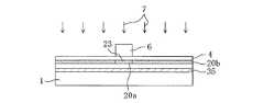
図1〜図11は、本発明に係る実施形態1にかかる断面図である。本実施形態1においては、一方の基板に半導体デバイス部Tを全て形成した後、他の基板K(以下、基板Kと称する。)に貼り合せて半導体装置Sを形成する場合について説明する。また、説明の便宜上、上下左右といった位置或いは方向を示す記載については、図面を正面視した場合を基準として記載している。
FIGS. 1-11 is sectional
なお、通常、半導体デバイス部Tは複数個のNMOSトランジスタ及び/またはPMOSトランジスタが同一基板上に複数作りこまれた構造となるものであるが、説明をわかり易く簡素化するため、1個のNMOSトランジスタを形成する場合を例として説明する。PMOSトランジスタについては示さないが、イオン注入時の不純物導電型を適宜変更することでNMOSトランジスタと同様に形成できる。なお、この記載は単一のトランジスタを形成する場合を除外する意図ではない。また、ここでは、素子分離やウェル形成プロセスについて記載していないが、素子分離やウェル形成を行うようにしても構わない。 In general, the semiconductor device portion T has a structure in which a plurality of NMOS transistors and / or PMOS transistors are formed on the same substrate. However, in order to simplify the explanation, one NMOS transistor is used. The case of forming the film will be described as an example. Although the PMOS transistor is not shown, it can be formed in the same manner as the NMOS transistor by appropriately changing the impurity conductivity type during ion implantation. This description is not intended to exclude the case of forming a single transistor. Although element isolation and well formation processes are not described here, element isolation and well formation may be performed.
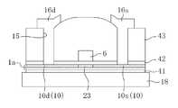
図1は、半導体デバイス部Tを基板Kに貼り合せ半導体基板Sを形成した後の状態を模式的に示す断面図である。すなわち、半導体基板Sは、基板Kと、高密度且つ高精度に形成された半導体デバイス部Tとを含んで構成されている。 FIG. 1 is a cross-sectional view schematically showing the state after the semiconductor device portion T is bonded to the substrate K and the semiconductor substrate S is formed. That is, the semiconductor substrate S includes the substrate K and the semiconductor device portion T formed with high density and high accuracy.
上記基板Kとしては、ガラス基板18が例示できる。 An example of the substrate K is a
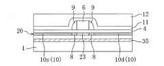
上記半導体デバイス部Tは、保護膜19、半導体層20、ゲート絶縁膜4、ゲート電極6、サイドウォール9、第1層間絶縁膜11、第2層間絶縁膜12、第3層間絶縁膜14、ソース電極16s、ドレイン電極16d、及び絶縁膜17を備え、チャネル領域23および低濃度不純物領域8によってLDD(Lightly Doped Drain)構造を有するMOSトランジスタ(NMOSトランジスタ)を構成している。 The semiconductor device portion T includes a
上記ゲート電極6は、第1層間絶縁膜11とゲート絶縁膜4との間に形成されている。すなわち、図1に示すように、第2層間絶縁膜12には凹部12aが形成され、この凹部12aの表面に沿って第1層間絶縁膜11が凹状に形成されている。上記ゲート電極6は、凹部12aの内部に第1層間絶縁膜11を介して設けられている。また、ゲート電極6の左右側面には、サイドウォール9がそれぞれ形成されている。そして、サイドウォール9及びゲート電極6の上面は、第1層間絶縁膜11の表面と同じ平面を構成している。そして、これらサイドウォール9、ゲート電極6、及び第1層間絶縁膜11の上には、ゲート絶縁膜4を介して半導体層20が設けられている。 The
上記半導体層20は、例えば不純物を有する単結晶シリコン層により構成される。そして、半導体層20は、チャネル領域23と、チャネル領域23の両外側に設けられた低濃度不純物領域8と、低濃度不純物領域8の両外側に設けられた高濃度不純物領域10とを備えている。 The
チャネル領域23は、ゲート絶縁膜4を介してゲート電極6の向かい側に対応して形成され、例えばホウ素等のP型不純物元素が1〜5×1017cm−3程度の濃度になるように注入されている。また、低濃度不純物領域8は、上記ゲート絶縁膜4を介して各サイドウォール9の向かい側に対応して形成されている。低濃度不純物領域8及び高濃度不純物領域10には、リン等のN型不純物元素が注入されており、低濃度不純物領域8は例えば1〜5×1018cm−3程度、高濃度不純物領域10は1×10¹⁹〜1×1020cm−3程度のように低濃度不純物領域8は高濃度不純物領域10よりも低い濃度で形成されている。言い換えれば、半導体層20における不純物濃度は、チャネル領域23、低濃度不純物領域8、及び高濃度不純物領域10の順に高くなっている。The
そして、上記各高濃度不純物領域10の一方がドレイン領域10dを構成する一方、他方がソース領域10sを構成している。さらに、ドレイン領域10dにはドレイン電極16dが接続されると共に、ソース領域10sにはソース電極16sが接続されている。 One of the high-
すなわち、図1に示すように、ドレイン領域10d及びソース領域10sの下方には、第3層間絶縁膜14、第2層間絶縁膜12、第1層間絶縁膜11、ゲート酸化膜4を上下に貫通するコンタクトホール15がそれぞれ形成されている。また、ドレイン領域10dおよびソース領域10sと電気的に接続するためにコンタクトホール15内に金属等の導電材料が充填され、上記ドレイン電極16d及びソース電極16sが形成されている。凹部17aは溝状に延びることにより、凹部17a内の導電材料が配線を構成するようになっている。以上のようにして、半導体デバイス部Tは構成されている。 That is, as shown in FIG. 1, below the
なお、ガラス基板18に対して、半導体デバイス部Tの構造が上下反転した構造であってもよい。 Note that the structure of the semiconductor device portion T may be inverted with respect to the
−製造方法−
次に、本実施形態の半導体基板S及び半導体デバイス部Tの製造方法について、図1〜図12を参照して説明する。-Manufacturing method-
Next, a method for manufacturing the semiconductor substrate S and the semiconductor device unit T according to this embodiment will be described with reference to FIGS.
半導体デバイス部Tの製造方法は、例えばイオン注入による拡散抑止層形成工程と、活性化工程と、例えばイオン注入による剥離層形成工程と、貼り合わせ工程(貼付工程)と、分割工程(剥離工程)と、除去工程とを備えている。 The manufacturing method of the semiconductor device portion T includes, for example, a diffusion suppression layer forming process by ion implantation, an activation process, a peeling layer forming process by, for example, ion implantation, a bonding process (sticking process), and a dividing process (peeling process). And a removal step.
さらに具体的には、半導体デバイス部Tの製造方法は、剥離用物質である水素、あるいは水素および希ガスを単結晶シリコン基板に注入して加熱することにより、単結晶シリコン基板の一部を分割除去する工程を含む製造方法であって、水素の透過拡散を抑止する拡散抑止層35を単結晶シリコン基板に形成する工程と、水素を含む剥離層36を単結晶シリコン基板に形成する工程と、熱処理を行うことにより剥離層36に沿って単結晶シリコン基板の一部を剥離する工程とを備えている。 More specifically, in the method of manufacturing the semiconductor device portion T, a part of the single crystal silicon substrate is divided by injecting hydrogen, which is a peeling material, or hydrogen and a rare gas into the single crystal silicon substrate and heating. A manufacturing method including a step of removing, a step of forming a
本実施形態では、半導体デバイス部Tを形成するデバイス部形成工程は、貼り合わせ工程よりも前に行われる。 In this embodiment, the device part forming process for forming the semiconductor device part T is performed before the bonding process.
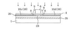
まず、図2に示すように、シリコンウェハ(単結晶シリコン基板)1の表面に保護膜である酸化膜2を20nmの厚みで形成する。その後、MOSトランジスタのしきい値制御の目的で、半導体層20のチャネル領域23を形成するための不純物元素であるホウ素3をイオン注入する。イオン注入の条件は、例えば、注入エネルギーを10〜30KeV程度とし、ドーズ量を1〜5×1012cm−2程度とする。このことにより、半導体層20aを酸化膜2の下方のシリコンウェハ1内に形成する。First, as shown in FIG. 2, an
次に、絶縁層形成工程では、図3に示すように、酸化膜2を除去した後に、シリコンウェハ1(後の半導体層20)の表面に絶縁層であるゲート絶縁膜4を形成する。ゲート絶縁膜4は例えば酸化膜であって、1000℃の酸化雰囲気中で熱処理を行うことにより、シリコンウェハ1の上に20nm程度の厚みに形成する。 Next, in the insulating layer forming step, as shown in FIG. 3, after the
その後、拡散抑止層形成工程では、図3に示すように、シリコンウェハ1に対し、シリコンウェハ1における剥離用物質(本例では水素)の移動を抑止するための拡散抑止用物質であるホウ素をイオン注入等により形成する。このことにより、シリコンウェハ1にホウ素を含む拡散抑止層35を形成する。拡散抑止層35は、半導体層20aよりも深い下方位置に形成する。言い換えれば、半導体層20aは、拡散抑止層35とゲート絶縁膜4との間に形成されている。このように、1000℃の酸化雰囲気で熱処理を行ってゲート絶縁膜4を形成した後に、水素の移動を抑止するためのホウ素を含む拡散抑止層35を形成することにより、熱処理によって拡散抑止層のホウ素元素がシリコンウェハ表面へ拡散することを極力抑えることができ、MOSトランジスタのしきい値電圧等の電気特性の制御性が悪化することを回避している。なお、ゲート絶縁膜4形成時の熱処理温度が低く、ホウ素元素の熱拡散の影響が小さい場合には、拡散抑止層35の形成をゲート絶縁膜4形成工程よりも以前に行っても問題ない。 Thereafter, in the diffusion suppressing layer forming step, as shown in FIG. 3, boron, which is a diffusion suppressing substance for suppressing the movement of the peeling material (hydrogen in this example) on the
上記拡散抑止層35は、半導体デバイス部TであるNMOSトランジスタの電気特性に影響を与えないような深さに形成されている。すなわち、後工程の熱処理により拡散抑止層35のホウ素がシリコンウェハ1の表面へ拡散してNMOSトランジスタのしきい値電圧に影響を与えないように、注入エネルギーを設定する。 The
ここで、プロセスシミュレーションから得られた、ホウ素を単結晶シリコン基板にイオン注入したときの単結晶シリコン基板の深さ位置と、ホウ素の濃度との関係を、図12に示す。ホウ素は、5×1014cm−2のドーズ量で注入した後、900℃で10分間熱処理を行ったものであり、注入エネルギーを、100,200,300,400,500KeVと設定した場合について、それぞれ深さ方向の濃度分布を調べた。Here, FIG. 12 shows the relationship between the depth position of the single crystal silicon substrate and the concentration of boron obtained by ion implantation of boron into the single crystal silicon substrate, obtained from the process simulation. Boron was implanted at a dose of 5 × 1014 cm−2 and then heat treated at 900 ° C. for 10 minutes, and the implantation energy was set to 100, 200, 300, 400, 500 KeV. The concentration distribution in the depth direction was examined.
図12に示すように、ホウ素濃度は、単結晶シリコン基板の表面から深くなるに連れて徐々に高くなり、所定の深さでピークに達する。その後、ホウ素濃度は、深くなるに連れて低くなっていることがわかる。この分布は、シリコンウェハ表面側がその反対側よりもなだらかな曲線を描いて減少する態様となる。すなわち、注入ピーク位置を中心に深さ方向で非対称なピアソン分布となる。また、上記拡散抑止層は、上記濃度分布のうち所定濃度以上となる範囲として規定される。所定濃度とは、例えば注入ピーク位置での濃度の10分の1である。また、注入エネルギーが大きいほど、ホウ素濃度が高くなるピーク深さが、深い位置へ移ることがわかる。 As shown in FIG. 12, the boron concentration gradually increases with increasing depth from the surface of the single crystal silicon substrate, and reaches a peak at a predetermined depth. Thereafter, it can be seen that the boron concentration decreases as the depth increases. This distribution is such that the surface side of the silicon wafer decreases with a gentler curve than the opposite side. In other words, the Pearson distribution is asymmetric in the depth direction around the injection peak position. Further, the diffusion suppression layer is defined as a range in which the predetermined concentration or more is reached in the concentration distribution. The predetermined concentration is, for example, one tenth of the concentration at the injection peak position. It can also be seen that the peak depth at which the boron concentration increases as the implantation energy increases, moves to a deeper position.
ところで、シリコンウェハ1の表面における半導体デバイス部完成時点におけるホウ素濃度は1×1017cm−3以下であることが好ましい。ホウ素濃度が1×1017cm−3よりも高い場合には、MOSトランジスタのチャネル領域23における不純物濃度が高くなりすぎるので、しきい値の制御が困難になり、所望のしきい値を得にくくなってしまうためである。By the way, it is preferable that the boron concentration at the time of completion of the semiconductor device portion on the surface of the
また、シリコンウェハ表面における拡散抑止用ホウ素元素の濃度は、イオン注入条件のドーズ量、注入エネルギー、および半導体デバイス形成プロセス中の熱処理条件の関数として与えられる。例えば、900℃10分間熱処理でのチャネル領域23のゲート電極6側の表面濃度が1×1017cm−3以下を満たすようなホウ素のドーズ量及び注入エネルギー領域は図33の実線よりも下方の領域となる。従って、900℃10分間熱処理でのシリコンウェハ1の表面濃度が1×1017cm−3以下を満たすホウ素のドーズ量D(cm-2)と注入エネルギーE(KeV)の条件は、
D≦2.7×10⁸×E2.78・・・・・・・・・・・・(1)
となる。Further, the concentration of the boron element for suppressing diffusion on the surface of the silicon wafer is given as a function of the dose amount of the ion implantation conditions, the implantation energy, and the heat treatment conditions during the semiconductor device formation process. For example, the boron dose amount and the implantation energy region in which the surface concentration on the
D ≦ 2.7 × 10⁸ × E2.78 (1)
It becomes.
また、一般にICのMOSトランジスタにおけるチャネル領域23の不純物濃度は1〜5×1017cm−3程度であることから、水素に起因して発生するN型不純物濃度が1×1017cm−3程度未満であれば、電気特性に与える影響は小さくなると考えられる。従って、水素に起因して発生するN型不純物濃度が1×1017cm−3程度以上の場合において対策を行えばよいと考えられる。1×1017cm−3程度をドーズ量に換算すると、ホウ素元素の必要下限ドーズ量は1×1012cm−2となる。In general, since the impurity concentration of the
以上をまとめると、ホウ素元素のドーズ量D(cm-2)と注入エネルギーE(KeV)としたとき、好ましいホウ素イオンの注入条件は、
1×1012cm−2≦D≦2.7×10⁸×E2.78・・・(2)
となる。これは、図33の斜線部分に相当する。To summarize the above, when the boron element dose D (cm−2 ) and the implantation energy E (KeV) are used, the preferred boron ion implantation conditions are:
1 × 1012 cm−2 ≦ D ≦ 2.7 × 10⁸ × E2.78 (2)
It becomes. This corresponds to the hatched portion in FIG.
従って、上記(2)の条件を満たすようにイオン注入を行なえば、好適に作動するチャネル領域をシリコンウェハに形成することが可能となる。なお、上記にはチャネル領域23のゲート電極6側の拡散抑止用ホウ素の表面濃度が1×1017cm−3以下を満たすものについて記載したがそれに限られない。すなわち、半導体層20の拡散抑止用ホウ素の表面濃度が1×1017cm−3以下を満たすようにしても、好適に作動させることができる。Therefore, if ion implantation is performed so as to satisfy the above condition (2), a channel region that operates suitably can be formed in the silicon wafer. In the above description, the surface concentration of the diffusion suppressing boron on the
その後、図4に示すように、ゲート絶縁膜4の表面にゲート電極6を形成する。まず、ポリシリコンを300nm程度の厚さにCVD法等により堆積する。さらに、上記ポリシリコン層にN型不純物を拡散させてN型ポリシリコンとした後、フォトリソグラフィ等によりゲート電極6をパターン形成する。 Thereafter, as shown in FIG. 4, a
続いて、図4に示すように、ゲート電極6をマスクとしてN型不純物元素7をイオン注入し、不純物濃度が半導体層20aとは異なる半導体層20b(後の低濃度不純物領域8)を形成する。このとき、イオン注入されなかったゲート電極6の下方の半導体層20aは、チャネル領域23となる。 Subsequently, as shown in FIG. 4, an N-
次に、図5に示すように、ゲート電極6の左右の側壁部分に例えばSiO2のような絶縁性材料により構成されるサイドウォール9を形成する。続いて、上記ゲート電極6及びサイドウォール9をマスクとしてN型不純物元素5をイオン注入し、高濃度不純物領域10を形成する。このとき、サイドウォール9によりマスクされて不純物5が注入されなかった半導体層20bは、低濃度不純物領域8として形成される。Next, as shown in FIG. 5,
続いて、図6に示すように、上記ゲート絶縁膜4、ゲート電極6、及びサイドウォール9を覆うように、例えばSiO2のような絶縁性材料による第1層間絶縁膜11を100nm程度の厚みでCVD等により形成する。Subsequently, as shown in FIG. 6, a first
その後、活性化工程を行う。活性化工程では、熱処理によりイオン注入によってシリコンウェハ中に導入された不純物元素の活性化を行う。熱処理としては例えば900℃で10分間の処理を行うことが好ましい。このことにより、拡散抑止層35のホウ素イオンが加熱により活性化する。なお、熱処理温度は、ホウ素イオンの拡散をなるべく抑えるためにより低温であることが望ましい。また、RTA(ラピッドサーマルアニール)などの短時間熱処理も好ましい。このことにより、注入されたホウ素イオン13は、シリコン元素(Si)の置換位置に収まってドナー不純物となる。 Thereafter, an activation process is performed. In the activation step, the impurity element introduced into the silicon wafer by ion implantation is activated by heat treatment. For example, the heat treatment is preferably performed at 900 ° C. for 10 minutes. As a result, the boron ions in the
次に、図7に示すように、上記第1層間絶縁膜11を覆うように、第2層間絶縁膜12を形成した後、第2層間絶縁膜12の表面を、例えばCMP(Chemical Mechanical Polishing)等により平坦化する。尚、表面を平坦化する方法は、CMPに限らない。また、第2層間絶縁膜12を形成する代わりに第1層間絶縁膜11を厚く形成し、この第1層間絶縁膜11の表面をCMPにより平坦化するようにしても構わない。 Next, as shown in FIG. 7, after the second
次に、剥離層形成工程では、図8に示すように、剥離用物質である水素イオンをイオン注入によりシリコンウェハ1の内部に導入する。このことにより、シリコンウェハ1の領域のうち拡散抑止層35を介してゲート絶縁膜4と反対側の領域に剥離層36を形成する。注入条件としては、例えばドーズ量を1×1016cm−2以上且つ5×1016cm−2以下とし、注入エネルギーを150KeV以上とすることが好ましい。なぜなら、ドーズ量が1×1016cm−2よりも小さい場合には、熱処理時に水素注入ピーク位置でマイクロクラックが発生せず、シリコンウェハの分離ができなくなるという問題があるためであり、ドーズ量が5×1016cm−2よりも大きい場合には、シリコン基板表面付近にイオン注入による結晶欠陥が多数形成され、結晶性が悪化するという問題があるためである。上記の条件でイオン注入を行なうことにより、シリコン層における所望の深さに水素を含む剥離層36を形成することが可能となる。なお、剥離層36は、剥離用物質の濃度分布のピークを含む層をいう。Next, in the peeling layer forming step, as shown in FIG. 8, hydrogen ions, which are a peeling material, are introduced into the
その後、図9に示すように、上記第2層間絶縁膜12を覆うように、第3層間絶縁膜14を形成する。続いて、上記ドレイン領域10d及びソース領域10sの上方位置において、第3層間絶縁膜14、第2層間絶縁膜12、第1層間絶縁膜11、ゲート絶縁膜4を上下に貫通するコンタクトホール15を開口する。そして、各コンタクトホール15の内部に金属等の導電材料を充填することにより、ドレイン電極16d及びソース電極16sを形成する。なお、図示しないが、この後に200nm程度の窒化膜を形成し、その後に水素化処理を行ってもよい。 Thereafter, as shown in FIG. 9, a third
続いて、図10に示すように、第3層間絶縁膜の14上に、ドレイン電極16d及びソース電極16sを覆うように、SiO2等の絶縁膜17を形成し、この絶縁膜17の表面をCMP等により平坦化する。その後、シリコンウェハ1を所望の大きさにダイシング等により分断する。以下、この分断後のシリコンウェハ1をシリコン基板1として記載する。Subsequently, as shown in FIG. 10, an insulating
そして、RCA洗浄等のシリコン基板1の表面洗浄処理を行った後、位置あわせを行う。そして、貼り合わせ工程を行い、半導体デバイス部Tの絶縁膜17の表面をガラス基板18に貼り合わせる。このようにして、図10に示すように、シリコン基板1の表面に、ガラス基板18を貼り付ける。 Then, after performing the surface cleaning process of the
次に、剥離工程を行う。剥離工程では、図11に示すように、例えば600℃の温度環境下で数分間程度の間、熱処理することにより、シリコン基板1の一部を剥離層36に沿って剥離する。このことにより、シリコン基板1は薄膜化され、半導体デバイス部T(NMOSトランジスタ)は、半導体層20と共にガラス基板18上に配置されることとなる。トランジスタの特性に影響を与えないように、水素の拡散を抑制するためには、上記熱処理温度をなるべく低温にすると共に、熱処理時間を短くすることが望ましい。 Next, a peeling process is performed. In the peeling step, as shown in FIG. 11, a part of the
次に、除去工程において、図1に示すように、半導体層20に対し、拡散抑止層35を半導体層20に残留している水素と共にエッチング等により除去する。 Next, in the removing step, as shown in FIG. 1, the
除去方法としては、ドライエッチングやウエットエッチング、又はそれら両方を組み合わせることが可能である。ただし、ドライエッチングのみによると、半導体シリコン層20の表面にダメージが入る虞れがあるため、ドライエッチング後に適当なウェットエッチングを行うことが好ましい。シリコン基板1の一部が除去された結果、半導体シリコン層20の膜厚は、50〜200nm程度となる。なお、除去方法として、CMP(Chemical Mechanical Polshing)を適用してもよい。 As a removal method, dry etching, wet etching, or a combination of both can be used. However, since only dry etching may damage the surface of the
このように、除去工程が行われた結果、半導体層20内での、水素元素起因で発生するN型不純物濃度を、トランジスタの特性に影響を及ぼさない1×1017cm−3以下に抑えることができる。As described above, as a result of the removal step, the concentration of the N-type impurity generated in the
なお、水素元素起因で発生するN型不純物濃度をさらに低くすることが好ましい。その後、半導体層20の表面に絶縁性の保護膜19を形成する。なお、半導体層20と保護膜19の界面状態を改善するために、保護膜19形成前に半導体層20の表面を酸化して酸化膜を形成してもよい。 It is preferable to further reduce the concentration of N-type impurities generated due to the hydrogen element. Thereafter, an insulating
以上のように、シリコン基板1に、拡散抑止層35と、剥離層36とを形成し、熱処理を行うことにより剥離層36に沿ってシリコン基板1の一部を剥離すると共に、剥離層36に配された剥離用物質である水素等が拡散抑止層35を超えて拡散することを抑止する手法を用いて半導体装置Sを製造する。 As described above, the
なお、この製造方法により製造される半導体装置S、或いはその中間過程で製造されるシリコンウェハ、シリコン基板はすべて本発明にいう「半導体基板」の概念に含まれるものであるが、いずれの半導体基板においてもこの製造方法を用いて形成した場合は、剥離層及び拡散抑止層をイオン注入によって形成しているため、シリコン基板1に形成された水素及びホウ素の濃度分布が、基板の一面側から他面側に向かって傾斜しているようになる。 The semiconductor device S manufactured by this manufacturing method, or the silicon wafer and silicon substrate manufactured in the intermediate process are all included in the concept of “semiconductor substrate” in the present invention. In this case, since the peeling layer and the diffusion suppressing layer are formed by ion implantation, the concentration distribution of hydrogen and boron formed on the
−実施形態1の効果−
以上のとおりであるので、この実施形態1によると、剥離工程における熱処理時に拡散抑止層35に配置されたホウ素の作用により、剥離用物質である水素をトラップできるため、水素が拡散抑止層35を越えて半導体層20側に拡散することを防止できる。従って、剥離工程において、水素が半導体層20に拡散することに起因して半導体層20の電気特性が悪影響を受けることを抑止することが可能である。-Effect of Embodiment 1-
As described above, according to the first embodiment, hydrogen, which is a peeling material, can be trapped by the action of boron disposed in the
さらに、除去工程において、拡散抑止層35を半導体層20に残留している水素と共に除去するようにしたので、半導体デバイス部Tが水素により悪影響を受ける虞れをより確実に防止することができる。 Furthermore, since the
さらに、半導体層20をガラス基板18へ移す前に、半導体デバイス部Tを予め形成するようにしたので、ICプロセスでサブミクロンデバイスとして作製した半導体デバイス部Tをガラス基板18上に形成することができる。従って、通常ガラス基板に多結晶シリコン層や非晶質シリコン層を形成して半導体デバイス部を形成する場合と異なり、単結晶シリコン基板上に形成したトランジスタと同等もしくは薄膜化を行うことによりそれ以上の性能を有するトランジスタを、トランジスタの閾値制御性を悪化させることなく形成できる。 Furthermore, since the semiconductor device portion T is formed in advance before the
《発明の実施形態2》
図13〜図23は、本発明に係る半導体基板の実施形態2にかかる半導体装置、及びその製造方法を示す断面図である。尚、以降の各実施形態では、図1〜図11と同じ部分に同じ符号を付して、その詳細な説明を省略する。<<
13 to 23 are cross-sectional views showing a semiconductor device according to
本実施形態は、半導体層20を後に形成するシリコン基板層Lを予め他の基板Kへ移した後に、半導体デバイス部Tの形成工程を施すようにしたものである。 In the present embodiment, after the silicon substrate layer L to be formed later on the
なお、通常、半導体デバイス部Tは複数個のNMOSトランジスタ及び/またはPMOSトランジスタが同一基板上に複数作りこまれた構造となるものであるが、説明をわかり易く簡素化するため、1個のNMOSトランジスタを形成する場合を例として説明する。PMOSトランジスタについては示さないが、イオン注入時の不純物導電型を適宜変更することでNMOSトランジスタと同様に形成できる。なお、この記載は単一のトランジスタを形成する場合を除外する意図ではない。また、ここでは、素子分離やウェル形成プロセスについて記載していないが、素子分離やウェル形成を行うようにしても構わない。 In general, the semiconductor device portion T has a structure in which a plurality of NMOS transistors and / or PMOS transistors are formed on the same substrate. However, in order to simplify the explanation, one NMOS transistor is used. The case of forming the film will be described as an example. Although the PMOS transistor is not shown, it can be formed in the same manner as the NMOS transistor by appropriately changing the impurity conductivity type during ion implantation. This description is not intended to exclude the case of forming a single transistor. Although element isolation and well formation processes are not described here, element isolation and well formation may be performed.
図13は、基板Kと、シリコン基板層Lを含む半導体デバイス部Tとにより構成された半導体装置Sを模式的に示す断面図である。 FIG. 13 is a cross-sectional view schematically showing a semiconductor device S composed of a substrate K and a semiconductor device portion T including a silicon substrate layer L.
基板Kは、ガラス基板18が例示できる。 An example of the substrate K is a
上記半導体デバイス部Tは、酸化膜41、半導体層20、ゲート絶縁膜42、ゲート電極6、層間絶縁膜43、ソース電極16s、ドレイン電極16d、及びシリコン窒化膜44を備え、チャネル領域23、ドレイン領域10d、及びソース領域10sによってMOSトランジスタ(NMOSトランジスタ)を構成している。 The semiconductor device portion T includes an
半導体層20は、チャネル領域23と、チャネル領域23の両外側に設けられた高濃度不純物領域10とを備えている。高濃度不純物領域10は、ドレイン領域10dとソース領域10sとにより構成されている。そして、上記層間絶縁膜43には、ドレイン領域10d及びソース領域10sの各上方位置にコンタクトホール15が形成され、各コンタクトホール15の内部に、ドレイン領域10dに接続されたドレイン電極16dと、ソース領域10sに接続されたソース電極16sとが形成されている。 The
そして、上記層間絶縁膜43の上には、ドレイン電極16d及びソース電極16sを覆うようにシリコン窒化膜44が形成されている。 A
−製造方法−
次に、本実施形態の半導体装置S、及びシリコン基板層Lを含む半導体デバイス部Tの製造方法について、図13〜図23を参照して説明する。-Manufacturing method-
Next, a method for manufacturing the semiconductor device S of this embodiment and the semiconductor device portion T including the silicon substrate layer L will be described with reference to FIGS.
本実施形態のシリコン基板層Lの製造方法は、上記実施形態1と同様に、拡散抑止層形成工程と、活性化工程と、剥離層形成工程と、貼り合わせ工程(貼付工程)と、剥離工程(分割工程)と、除去工程とを備えている。また、本実施形態の半導体装置Sの製造方法は、上記実施形態1と同様に、上記シリコン基板層Lの製造方法に加えて、さらに、ゲート絶縁膜、ゲート電極、ソースおよびドレイン領域形成、層間絶縁膜形成、コンタクトホール形成、ソース及びドレイン電極形成、シリコン窒化膜形成等のゲート絶縁膜以降のデバイス部形成工程を備えているが、上記実施形態1とは、それらゲート絶縁膜以降のデバイス部形成工程を行うタイミングが異なっている。 The manufacturing method of the silicon substrate layer L of the present embodiment is similar to the first embodiment described above, in the diffusion suppression layer forming step, the activation step, the release layer forming step, the bonding step (sticking step), and the peeling step. (Dividing step) and a removing step. In addition to the method for manufacturing the silicon substrate layer L, the method for manufacturing the semiconductor device S according to the present embodiment further includes forming a gate insulating film, a gate electrode, source and drain regions, and an interlayer. The device portion forming process after the gate insulating film such as insulating film formation, contact hole formation, source and drain electrode formation, silicon nitride film formation and the like is provided. The first embodiment is a device portion after the gate insulating film. The timing for performing the forming process is different.
すなわち、上記実施形態1では、拡散抑止層形成工程、活性化工程、及び剥離層形成工程と並行してデバイス部形成工程を行うようにしたが、本実施形態では、ゲート絶縁膜形成以降のデバイス部形成工程を、除去工程の後に行う。 That is, in the first embodiment, the device part forming step is performed in parallel with the diffusion suppressing layer forming step, the activation step, and the release layer forming step. However, in this embodiment, the device after the gate insulating film formation is performed. The part forming step is performed after the removing step.
まず、絶縁層形成工程において、図14に示すように、シリコンウェハ1に基板表面を保護するための絶縁層である酸化膜41を20nm程度の厚みで形成する。 First, in the insulating layer forming step, as shown in FIG. 14, an
その後、拡散抑止層形成工程では、図15に示すように、拡散抑止用物質であるホウ素5をシリコンウェハ1に注入し、拡散抑止層35を形成する。ホウ素5の注入条件は、上記実施形態1とほぼ同様である。その結果、シリコンウェハ1の表面において拡散抑止用物質の濃度が1×1017cm−3以下であれば後に半導体デバイス部を形成した際にも略閾値制御に影響を与えないものとすることができる。Thereafter, in the diffusion suppressing layer forming step, as shown in FIG. 15,
続いて、熱処理等による活性化工程において、拡散抑止層35のホウ素を活性化する。上記実施形態と同様の条件が使用できる。また、熱処理温度は、ホウ素の拡散をなるべく抑えるためにより低温であることが望ましい点も同様である。 Subsequently, boron in the
なお、図20で示す後工程において行うシリコンウェハ1中にチャネル領域23を形成するためのホウ素3のイオン注入工程を上記熱処理の前に行ってもよい。この利点としては、貼り合わせ工程の後にガラス基板18上で行われるイオン注入工程がイオンドーピング装置によって行われる場合には、所望の不純物元素以外の元素が同時にチャネル領域23に導入される問題があるため、しきい値電圧制御が難しくなる問題があるが、イオン注入装置の場合には、質量分離装置により所望の元素のみを注入することができるため、しきい値電圧制御性が向上する点が挙げられる。 Note that an ion implantation step of
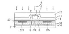
次に、剥離層形成工程では、図16に示すように、剥離用物質13である水素元素をイオン注入等によりシリコンウェハ1の内部に導入する。このことにより、拡散抑止層35よりも下方位置に剥離層36を形成する。 Next, in the peeling layer forming step, as shown in FIG. 16, a hydrogen element as the peeling
ここまでの工程により形成されたシリコンウェハ1は、ガラス基板上に単結晶シリコン薄膜を形成する場合に有用である。すなわち、例えば室温でガラス基板に貼り合わせた後、600℃程度の熱処理を行うことによって、膜厚均一性に優れた単結晶シリコン薄膜を容易にガラス基板上に形成することが可能となる。このとき、熱拡散により単結晶シリコン薄膜側へ移動しようとする水素元素をホウ素イオンが阻止するため、水素元素起因により単結晶シリコン薄膜がN型化するのを防ぐことができる。その結果、その後に形成するNMOSおよびPMOSトランジスタのしきい値を所望の値に容易に制御できると共に、水素元素起因のしきい値変動を抑えて再現性良くトランジスタを形成できる。また、ここまでの工程により形成されたシリコンウェハ1はシリコンウェハの形状であるため、別の場所に移動する場合にも、シリコンウェハ用キャリアなどに入れて容易に持ち運びできるなど、取り扱いやすい等の利点がある。 The
そして、シリコンウェハ1をダイシング等により分断してシリコン基板1とする。そして、RCA洗浄等によってシリコン基板1の表面洗浄処理を行った後、貼り合わせ工程を行う。貼り合せ工程では、図17に示すように、基板を上下に反転して下面(すなわち、酸化膜41)の表面にガラス基板18を貼り合わせる。その後、分割工程では例えば600℃の温度環境下で数分間程度の間熱処理することにより、図18に示すように、シリコン基板1を剥離層36に沿って分割して剥離する。そして、ガラス基板18側に残ったシリコン基板1の一部が薄膜シリコン基板1aとして形成される。 Then, the
次に、除去工程において、図19に示すように、薄膜シリコン基板1aに対し、拡散抑止層35及び剥離層36を実施形態1と同様にエッチング等により除去する。以上の工程によってシリコン基板層Lが製造される。なお、拡散抑止層35の除去に引き続いて、エッチング等によりシリコン基板層Lを所望の膜厚に調整してもよい。 Next, in the removing step, as shown in FIG. 19, the
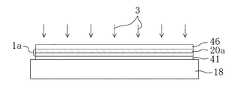
続いて、以下の半導体デバイス形成工程を行い、半導体装置Sを製造する。 Subsequently, the semiconductor device S is manufactured by performing the following semiconductor device formation process.
すなわち、図20に示すように、薄膜シリコン基板1aの表面を保護するために、CVD法等により酸化膜46を20nm程度形成した後、薄膜シリコン基板1aのチャネル領域23を形成するための不純物元素であるホウ素3をイオン注入する。このことにより、半導体層20aを酸化膜2の下方の薄膜シリコン基板1a中に形成する。 That is, as shown in FIG. 20, in order to protect the surface of the thin
次に、図21に示すように、酸化膜46を除去した後に、薄膜シリコン基板1aの表面にゲート絶縁膜42を形成する。ゲート絶縁膜42は、CVD法等によりSiO2膜を60nm程度の厚みに形成する。次に、高濃度のN型又はP型の不純物を含んだポリシリコン、あるいはW、Ta、TaNといった金属材料や、シリサイド等の材料を用いてゲート電極6を形成する。Next, as shown in FIG. 21, after the
その後、ゲート電極6をマスクとして、N型不純物元素5を半導体層20aに注入し、高濃度不純物領域10を形成する。高濃度不純物領域10は、ドレイン領域10dとソース領域10sとにより構成されている。このとき、ゲート電極6の下方の半導体層20aは、チャネル領域23となる。尚、高濃度不純物領域10とチャネル領域23との間にN型低濃度不純物領域を設けることにより、LDD構造とすることも可能である。 Thereafter, using the
続いて、図22に示すように、ゲート酸化膜42の上に、層間絶縁膜43を700nm程度の厚みで形成する。その後、レーザー、RTA、及び炉等により熱処理を行うことにより不純物元素を活性化させる。 Subsequently, as shown in FIG. 22, an
次に、図23に示すように、層間絶縁膜43及びゲート酸化膜42を上下に貫通するコンタクトホール15を、ドレイン領域10d及びソース領域10sの上方位置に形成する。そして、上記各コンタクトホール15に金属等の導電材料を充填することによりドレイン電極16d及びソース電極16sを形成する。 Next, as shown in FIG. 23, contact holes 15 that vertically penetrate the
その後、図13に示すように、シリコン窒化膜44を200nm程度の厚みで形成し、水素化処理を行う。以上のようにして半導体装置Sを製造する。 Thereafter, as shown in FIG. 13, a
なお、この製造方法により製造される半導体装置S、或いはその中間過程で製造されるシリコンウェハ、シリコン基板、および薄膜シリコン基板が貼り合わされたガラス基板はいずれも本発明にいう「半導体基板」の概念に含まれるものであるが、いずれの半導体基板においてもこの製造方法を用いて形成した場合は、剥離層及び拡散抑止層をイオン注入によって形成しているため、水素及びホウ素の濃度分布が基板の一面側から他面側に向かって傾斜しているようになる。 The semiconductor device S manufactured by this manufacturing method, or the silicon wafer manufactured in the intermediate process, the silicon substrate, and the glass substrate on which the thin film silicon substrate is bonded together are all referred to as the “semiconductor substrate” in the present invention. However, when any semiconductor substrate is formed using this manufacturing method, the separation layer and the diffusion suppression layer are formed by ion implantation, so that the concentration distribution of hydrogen and boron is It becomes inclined from the one surface side toward the other surface side.
−実施形態2の効果−
したがって、この実施形態によると、活性化されたホウ素により水素をトラップできるため、水素が後に半導体層20を形成する領域へ移動することを防げる。その結果、その後のデバイス形成工程において、閾値制御性が悪化せず、良好な特性のトランジスタを形成することが可能となる。-Effect of Embodiment 2-
Therefore, according to this embodiment, since hydrogen can be trapped by the activated boron, it is possible to prevent the hydrogen from moving to a region where the
また、上記の製造方法によれば、しきい値制御性が良く、特性ばらつきの小さな薄膜単結晶シリコン基板をガラス基板上に形成できるので、ガラス基板上に形成された多結晶シリコンや非晶質シリコンとは異なり、単結晶シリコン基板上に形成するトランジスタと同等もしくはそれ以上の高性能な電気特性を有するトランジスタを形成することができる。 In addition, according to the above manufacturing method, a thin film single crystal silicon substrate with good threshold controllability and small characteristic variation can be formed on a glass substrate, so that polycrystalline silicon or amorphous formed on the glass substrate can be formed. Unlike silicon, a transistor having high-performance electrical characteristics equivalent to or higher than that of a transistor formed over a single crystal silicon substrate can be formed.
また、薄膜単結晶シリコン基板を複数個ガラス基板に貼り合わせることも可能であるので、ガラス基板の大きさに制限されることなく、任意の位置に単結晶シリコン層をガラス基板上に形成することが可能であり、例えば、どんな大きさのガラス基板であっても単結晶薄膜シリコン基板を容易にレイアウトすることも可能となる。 In addition, since it is possible to attach a plurality of thin film single crystal silicon substrates to a glass substrate, a single crystal silicon layer is formed on the glass substrate at an arbitrary position without being limited by the size of the glass substrate. For example, a single crystal thin film silicon substrate can be easily laid out regardless of the size of the glass substrate.
《発明の実施形態3》
図24〜図32は、本発明に係る半導体基板の実施形態3にかかる半導体装置、及びその製造方法を示す断面図である。<<
24 to 32 are cross-sectional views illustrating a semiconductor device according to
本実施形態では、貼り合わせ工程(貼付工程)の前工程において半導体デバイス部Tの一部を形成する一方、上記貼り合わせ工程の後工程においてその他の一部を形成するようにしている。 In the present embodiment, a part of the semiconductor device portion T is formed in the pre-process of the bonding process (bonding process), while the other part is formed in the post-process of the bonding process.
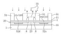
図24は、基板Kと半導体デバイス部Tとにより構成された半導体装置Sを模式的に示す断面図である。なお、通常、半導体デバイス部Tは複数個のNMOSトランジスタ及び/またはPMOSトランジスタ が同一基板上に複数作りこまれた構造となるものであるが、説明をわかり易く簡素化するため、1個のNMOSトランジスタを形成する場合を例として説明する。PMOSトランジスタについては示さないが、イオン注入時の不純物導電型を適宜変更することでNMOSトランジスタと同様に形成できる。なお、この記載は単一のトランジスタを形成する場合を除外する意図ではない。また、ここでは、素子分離やウェル形成プロセスについて記載していないが、素子分離やウェル形成を行うようにしても構わない。 FIG. 24 is a cross-sectional view schematically showing a semiconductor device S composed of a substrate K and a semiconductor device portion T. In general, the semiconductor device portion T has a structure in which a plurality of NMOS transistors and / or PMOS transistors are formed on the same substrate. However, in order to simplify the explanation, one NMOS transistor is used. The case of forming the film will be described as an example. Although the PMOS transistor is not shown, it can be formed in the same manner as the NMOS transistor by appropriately changing the impurity conductivity type during ion implantation. This description is not intended to exclude the case of forming a single transistor. Although element isolation and well formation processes are not described here, element isolation and well formation may be performed.
基板Kとしては、ガラス基板18が例示できる。 An example of the substrate K is a
上記半導体デバイス部Tは、第2層間絶縁膜12、第1層間絶縁膜11、ゲート電極6、サイドウォール9、ゲート絶縁膜4、半導体層20、層間絶縁膜53、ソース電極16s、ドレイン電極16d、及びシリコン窒化膜44を備え、チャネル領域23およびLDD領域を有するMOSトランジスタ(NMOSトランジスタ)を構成している。 The semiconductor device portion T includes the second
すなわち、上記実施形態1と同様に、ゲート電極6は、上記第1層間絶縁膜11とゲート酸化膜4との間に形成され、左右側面には、サイドウォール9がそれぞれ形成されている。また、半導体層20は、チャネル領域23と、チャネル領域23の両外側に設けられた低濃度不純物領域8と、低濃度不純物領域8の両外側に設けられた高濃度不純物領域10とを備えている。 That is, as in the first embodiment, the
上記半導体層20には、図24に示すように、高濃度不純物領域52d,52sがドレイン領域10d及びソース領域10sにそれぞれ上下に重なるように形成されている。そして、層間絶縁膜53に形成されたコンタクトホール15には、ドレイン電極16d及びソース電極16sが設けられている。 In the
上記ドレイン電極16dは、高濃度不純物領域52dを介してドレイン領域10dに接続される一方、上記ソース電極16sは、高濃度不純物領域52sを介してソース領域10sに接続されている。従って、高濃度不純物領域52dとドレイン電極16及び高濃度不純物領域52sとソース電極16sは電気的に接続されている。これらドレイン電極16d及びソース電極16sは、層間絶縁膜53と共に、シリコン窒化膜54により被覆されている。 The
半導体デバイス部Tは、図24に示すように、半導体層−ゲート電極部Gと、コンタクト−電極部Iとにより構成されている。 As shown in FIG. 24, the semiconductor device portion T includes a semiconductor layer-gate electrode portion G and a contact-electrode portion I.
以上のようにして、半導体装置S及び半導体デバイス部Tは構成されている。 The semiconductor device S and the semiconductor device unit T are configured as described above.
−製造方法−
次に、本実施形態の半導体装置Sの製造方法と、半導体層−ゲート電極部G、及びコンタクト−電極部Iにより構成される半導体デバイス部Tの製造方法とについて、図24〜図32を参照して説明する。-Manufacturing method-
Next, a method for manufacturing the semiconductor device S of the present embodiment and a method for manufacturing the semiconductor device portion T including the semiconductor layer-gate electrode portion G and the contact-electrode portion I will be described with reference to FIGS. To explain.
本実施形態では、貼り合わせ工程の前工程において、半導体デバイス部Tの半導体層−ゲート電極部Gを形成する一方、貼り合わせ工程の後工程において、半導体デバイス部Tのコンタクト−電極部Iを形成する。 In the present embodiment, the semiconductor layer-gate electrode portion G of the semiconductor device portion T is formed in the pre-step of the bonding step, while the contact-electrode portion I of the semiconductor device portion T is formed in the post-step of the bonding step. To do.
本実施形態の半導体デバイス部Tの製造方法は、上記実施形態1と同様に、絶縁層形成工程と、拡散抑止層形成工程と、活性化工程と、剥離層形成工程と、貼り合わせ工程(貼付工程)と、分割工程(剥離工程)と、除去工程とを備えている。 The manufacturing method of the semiconductor device portion T according to the present embodiment is similar to the first embodiment described above in that the insulating layer forming step, the diffusion suppressing layer forming step, the activation step, the release layer forming step, and the bonding step (sticking) Step), a dividing step (peeling step), and a removing step.
まず、上記実施形態1におけるサイドウォール9及び高濃度不純物領域10の形成までの工程と同じ工程を行う(図2〜図5参照)。 First, the same steps as those up to the formation of the
その後、図25に示すように、レジストマスク51をパターン形成した後に、N型不純物55を高濃度不純物領域10に下方に隣接した所定の領域にイオン注入により導入する。こうして、高濃度不純物領域52d,52sを形成する。このように、高濃度不純物領域52d,52sを形成することにより、NMOSトランジスタのソース領域10s及びドレイン領域10dを構成する高濃度不純物領域10と、ガラス基板18への貼り合わせ工程以降の後工程にて形成するメタル配線であるソース電極16s及びドレイン電極16dとのコンタクトを確実に接続することが可能となる。 Thereafter, as shown in FIG. 25, after patterning the resist
例えば、N型不純物55のイオン注入条件としては、イオン種をリンとし、注入エネルギーを45KeV、ドーズ量を2×1015cm−2、及びイオン種をリンとし、注入エネルギーを100KeV、ドーズ量を2×1015cm−2として、2回の注入を行う。このことにより、高濃度不純物領域10から下方へ深さ約170nmのところまでの範囲に対し、電気的に導通を取ることができる。尚、高濃度不純物領域52d,52sの形成工程は必須ではない。For example, as ion implantation conditions for the N-
次に、図26に示すように、レジストマスク51を除去した後に、第1層間絶縁膜11を100nm程度の厚みで形成し、ゲート酸化膜4やゲート電極6等を被覆する。その後、活性化工程において、熱処理を行い、イオン注入によりシリコンウェハ中に導入された拡散抑止層35のホウ素を含む不純物元素を活性化する。熱処理としては、例えば900℃で10分間の処理を行う。 Next, as shown in FIG. 26, after removing the resist
続いて、図27に示すように、第2層間絶縁膜12を形成した後、表面を平坦化する。次に、剥離層形成工程では、図28に示すように、上記実施形態1と同様にして、剥離用物質である水素元素13をイオン注入によりシリコンウェハ1の内部に導入する。このことにより、拡散抑止層35よりも下方位置に剥離層36を形成する。 Subsequently, as shown in FIG. 27, after the second
そして、シリコンウェハ1をダイシング等により分断してシリコン基板1とする。そして、RCA洗浄等によってシリコン基板1の表面洗浄処理を行った後、貼り合わせ工程を行う。 Then, the
貼り合わせ工程では、図29に示すように、シリコン基板を上下に反転して下面の第2層間絶縁膜12の表面にガラス基板18を貼り合わせる。続いて、剥離工程では、図30に示すように、上記実施形態1と同様にして、シリコン基板1を剥離層36に沿って分割する。その結果、ガラス基板18側に、半導体層20からゲート電極部までの部分Gを含むシリコン基板1の一部が配置される。 In the bonding step, as shown in FIG. 29, the silicon substrate is turned upside down and the
続いて、除去工程において、図31に示すように、ガラス基板18上に配置されたシリコン基板1に対しエッチング等を施し、拡散防止層35と剥離層36を除去して半導体層20を露出させる。 Subsequently, in the removing step, as shown in FIG. 31, the
その後、図32に示すように、半導体層20の表面にCVD法等によって層間絶縁膜53を700nm程度の厚みで形成する。続いて、コンタクトホール15を高濃度不純物領域52d,52sに到達するように形成した後、コンタクトホール15に金属等の導電性材料を充填することによりドレイン電極16d及びソース電極16sを形成する。 Thereafter, as shown in FIG. 32, an
次に、図24に示すように、シリコン窒化膜54を200nm程度の厚みで形成し、水素化処理を行う。以上のようにして、半導体装置S及び半導体デバイス部Tを製造する。 Next, as shown in FIG. 24, a
なお、この製造方法により製造される半導体装置S、或いはその中間過程で製造されるシリコンウェハ、シリコン基板はいずれも本発明にいう「半導体基板」の概念に含まれるものであるが、いずれの半導体基板においてもこの製造方法を用いて形成した場合は、剥離層及び拡散抑止層をイオン注入によって形成しているため、水素及びホウ素の濃度分布が基板の一面側から他面側に向かって傾斜しているようになる。 The semiconductor device S manufactured by this manufacturing method, or the silicon wafer and silicon substrate manufactured in the intermediate process are all included in the concept of “semiconductor substrate” in the present invention. When the substrate is also formed using this manufacturing method, since the release layer and the diffusion suppression layer are formed by ion implantation, the concentration distribution of hydrogen and boron inclines from one side of the substrate toward the other side. Become like that.
−実施形態3の効果−
したがって、この実施形態によると他の実施形態と同様に、剥離用物質の悪影響が無く、しきい値制御性に優れ、しきい値ばらつきの小さな半導体シリコン薄膜を半導体層に用いることができる。-Effect of Embodiment 3-
Therefore, according to this embodiment, as in the other embodiments, a semiconductor silicon thin film that has no adverse effect of the peeling material, has excellent threshold controllability, and has small threshold variation can be used for the semiconductor layer.
また、ゲート電極形成までの工程においてシリコンICプロセスで作製したサブミクロンのゲート長を持つ高性能トランジスタをガラス基板上に形成することができる。このとき、半導体層は単結晶シリコンであるため、トランジスタの電気特性はシリコン上に作製したトランジスタに比べて遜色の無いものとなる。 In addition, a high-performance transistor having a submicron gate length manufactured by a silicon IC process can be formed on a glass substrate in the steps up to gate electrode formation. At this time, since the semiconductor layer is single crystal silicon, the electrical characteristics of the transistor are inferior to those of a transistor formed over silicon.
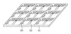
また、コンタクト形成以降の電極形成工程を貼り合わせ工程後に行うことから、図34に示すようにガラス基板61上にあらかじめ受動素子あるいは能動素子等の素子62を形成しておけば、受動素子あるいは能動素子等の素子62と単結晶シリコン層を有する半導体素子63とに対し、共通のコンタクト及びメタル配線等の層を同時に形成し、かつ、互いに電気的に接続することができるため、コスト上も有利となる。 Further, since the electrode formation process after the contact formation is performed after the bonding process, if the
また、位置合わせ精度良く貼り合わすことで、ガラス基板上の素子と単結晶シリコン層上の素子とをミクロンオーダーの近距離で接続できるため、集積度の向上も可能となる。また、分割工程における600℃程度の熱処理が配線材料に及ぼす影響を考慮する必要が無いため、配線材料の選択肢を広げることができる。その結果、例えばAlなど融点が低い材料を電極に使用できるので、Alの低抵抗率により電極の電気抵抗を大幅に下げることができ、トランジスタ特性及び信頼性を向上させることができる。 Further, by bonding with high alignment accuracy, the element on the glass substrate and the element on the single crystal silicon layer can be connected at a short distance of micron order, so that the degree of integration can be improved. In addition, since there is no need to consider the influence of the heat treatment at about 600 ° C. on the wiring material in the dividing step, the choice of wiring material can be expanded. As a result, since a material having a low melting point such as Al can be used for the electrode, the electrical resistance of the electrode can be greatly reduced due to the low resistivity of Al, and the transistor characteristics and reliability can be improved.
《その他の実施形態》
上記実施形態では、剥離用物質として水素イオンを適用したが、水素の代わりに水素と少なくとも1種類以上の不活性元素(例えばHe,Ne,Ar,Xe,Rn等)を注入するようにしてもよい。ヘリウムイオン等の不活性ガス元素は、電気的に不活性であり、不活性ガス元素の併用により水素元素濃度を減少させることができるため、水素元素によりトランジスタ等の半導体デバイス部Tに与える悪影響の度合いを軽減できる利点がある。ただし、注入工程を2回行う必要が生ずるデメリットがある。したがって、製造の容易化の観点からは、上述のように、剥離用物質には水素を適用することが好ましい。<< Other Embodiments >>
In the above embodiment, hydrogen ions are applied as the peeling material, but hydrogen and at least one inert element (for example, He, Ne, Ar, Xe, Rn, etc.) may be implanted instead of hydrogen. Good. Inert gas elements such as helium ions are electrically inactive, and the hydrogen element concentration can be reduced by the combined use of inert gas elements. There is an advantage that the degree can be reduced. However, there is a disadvantage that the injection process needs to be performed twice. Therefore, from the viewpoint of facilitating production, as described above, it is preferable to apply hydrogen to the peeling material.
また、上記実施形態にあっては、シリコン半導体基板の場合について示したが、本発明は、他の元素による化合物半導体も含めた半導体基板にも適用することが可能である。 In the above embodiment, the case of a silicon semiconductor substrate has been described. However, the present invention can also be applied to a semiconductor substrate including a compound semiconductor using other elements.
また、上記実施形態にあっては、あらかじめガラス基板上に受動素子あるいは能動素子等が設けられていてもよい。 Moreover, in the said embodiment, a passive element or an active element etc. may be previously provided on the glass substrate.
また、上記実施形態にあっては、MOS構造のみについて示したが、バイポーラトランジスタ、サイリスタ、接合トランジスタ、フォトニックデバイス等の各種半導体デバイスの形成においても、本発明を適用することが可能である。 In the above embodiment, only the MOS structure is shown, but the present invention can also be applied to the formation of various semiconductor devices such as bipolar transistors, thyristors, junction transistors, and photonic devices.
以上説明したように、本発明は、半導体基板の製造方法について有用であり、特に、単結晶シリコン基板に所定の元素イオンを注入して剥離層を形成し、熱処理により基板の一部を剥離して薄膜化する工程を含むものに適している。As described above, the present invention is useful witha semiconductor substrate manufacturinghow, particularly, the single crystal silicon substrate by injecting a predetermined element ions to form a release layer, a part of the substrate by heat treatment It is suitable for those including a process of peeling and thinning.
S 半導体装置(半導体基板)
K 基板
T 半導体デバイス部
G 半導体層−ゲート電極部
I コンタクト−電極部
1 半導体基板、シリコン基板
4 ゲート絶縁膜(絶縁層)
5 ホウ素(拡散抑止用物質)
13 水素(剥離用物質)
18 ガラス基板(基板)
20 半導体シリコン層(半導体層)
35 拡散抑止層(拡散抑止用物質含有層)
36 剥離層(剥離用物質含有層)S Semiconductor device (semiconductor substrate)
K substrate T semiconductor device part G semiconductor layer-gate electrode part I contact-
5 Boron (diffusion inhibiting substance)
13 Hydrogen (peeling material)
18 Glass substrate (substrate)
20 Semiconductor silicon layer (semiconductor layer)
35 Diffusion inhibition layer (Diffusion inhibition substance-containing layer)
36 Peeling layer (peeling substance-containing layer)
Claims (8)
Translated fromJapanese前記基板の一方の表面側に半導体デバイス部の少なくとも一部を形成する工程とを含む半導体基板の製造方法であって、
前記剥離層を形成する前に行われ、前記剥離層が形成される領域と前記半導体デバイス部の少なくとも一部が形成される領域との間に前記剥離用物質の透過拡散を抑止する拡散抑止層を形成する工程を有し、
前記拡散抑止層を形成する工程では、前記剥離用物質の拡散を抑止する拡散抑止用物質を前記基板の内部に導入することによって該基板の内部に前記拡散抑止層を形成することを特徴とする半導体基板の製造方法。Introducing a release material for peeling a part of the substrate into the substrate to form a release layer inside the substrate;
Forming at least a part of the semiconductor device portion on one surface side of the substrate,
A diffusion suppression layer that is performed before forming the release layer and suppresses permeation diffusion of the release material between a region where the release layer is formed and a region where at least a part of the semiconductor device portion is formed. Having a step of forming
In the step of forming the diffusion suppression layer, the diffusion suppression layer is formed inside the substrate by introducing a diffusion suppression material that suppresses diffusion of the peeling material into the substrate. A method for manufacturing a semiconductor substrate.
前記基板は、前記剥離層に沿って一部が剥離される前に、前記半導体デバイス部の少なくとも一部が形成されることを特徴とする請求項1に記載の半導体基板の製造方法。Having a step of peeling a part of the substrate along the release layer;
The method for manufacturing a semiconductor substrate according to claim 1, wherein at least a part of the semiconductor device portion is formed before the substrate is partially peeled along the peeling layer.
一部が剥離された前記基板から前記剥離層及び前記拡散抑止層を除去する工程とを有し、
前記剥離層及び前記拡散抑止層を前記基板から除去した後に、前記半導体デバイス部の少なくとも一部を形成することを特徴とする請求項1に記載の半導体基板の製造方法。Peeling a part of the substrate along the release layer;
Removing the release layer and the diffusion-inhibiting layer from the partially peeled substrate,
The method for manufacturing a semiconductor substrate according to claim 1, wherein at least a part of the semiconductor device portion is formed after removing the release layer and the diffusion suppression layer from the substrate.
前記基板の一方の表面側に半導体デバイス部の少なくとも一部を形成する工程と、
前記剥離層が形成された前記基板における前記半導体デバイス部の少なくとも一部が形成されている側を、他の基板に貼り付ける工程と、
前記他の基板に貼り付けられた前記基板の一部を、前記剥離層に沿って剥離する剥離工程とを有する半導体基板の製造方法であって、
前記剥離層を形成する前に行われ、前記剥離層が形成される領域と前記半導体デバイス部の少なくとも一部が形成される領域との間に前記剥離用物質の透過拡散を抑止する拡散抑止層を形成する工程を有し、
前記拡散抑止層を形成する工程では、前記剥離用物質の拡散を抑止する拡散抑止用物質を前記基板の内部に導入することによって該基板の内部に前記拡散抑止層を形成することを特徴とする半導体基板の製造方法。Introducing a release material for peeling a part of the substrate into the substrate to form a release layer inside the substrate;
Forming at least a portion of a semiconductor device portion on one surface side of the substrate;
A step of affixing, to another substrate, a side where at least a part of the semiconductor device portion of the substrate on which the release layer is formed is formed;
A method of manufacturing a semiconductor substrate, comprising: a peeling step of peeling a part of the substrate attached to the other substrate along the peeling layer,
A diffusion suppression layer that is performed before forming the release layer and suppresses permeation diffusion of the release material between a region where the release layer is formed and a region where at least a part of the semiconductor device portion is formed. Having a step of forming
In the step of forming the diffusion suppression layer, the diffusion suppression layer is formed inside the substrate by introducing a diffusion suppression material that suppresses diffusion of the peeling material into the substrate. A method for manufacturing a semiconductor substrate.
前記剥離層が形成された前記基板を、他の基板に貼り付ける工程と、
前記他の基板に貼り付けられた前記基板の一部を、前記剥離層に沿って剥離する剥離工程と、
前記一部が剥離された基板に半導体デバイス部の少なくとも一部を形成する工程とを有する半導体基板の製造方法であって、
前記剥離層を形成する前に行われ、前記剥離層が形成される領域と前記半導体デバイス部の少なくとも一部が形成される領域との間に前記剥離用物質の透過拡散を抑止する拡散抑止層を形成する工程を有し、
前記拡散抑止層を形成する工程では、前記剥離用物質の拡散を抑止する拡散抑止用物質を前記基板の内部に導入することによって該基板の内部に前記拡散抑止層を形成することを特徴とする半導体基板の製造方法。Introducing a release material for peeling a part of the substrate into the substrate to form a release layer inside the substrate;
Bonding the substrate on which the release layer is formed to another substrate;
A peeling step of peeling a part of the substrate attached to the other substrate along the peeling layer;
A step of forming at least a part of the semiconductor device portion on the substrate from which the part has been peeled,
A diffusion suppression layer that is performed before forming the release layer and suppresses permeation diffusion of the release material between a region where the release layer is formed and a region where at least a part of the semiconductor device portion is formed. Having a step of forming
In the step of forming the diffusion suppression layer, the diffusion suppression layer is formed inside the substrate by introducing a diffusion suppression material that suppresses diffusion of the peeling material into the substrate. A method for manufacturing a semiconductor substrate.
Priority Applications (4)
| Application Number | Priority Date | Filing Date | Title |
|---|---|---|---|
| JP2004181527AJP4814498B2 (en) | 2004-06-18 | 2004-06-18 | Manufacturing method of semiconductor substrate |
| US11/147,359US7563693B2 (en) | 2004-06-18 | 2005-06-08 | Method for manufacturing semiconductor substrate and semiconductor substrate |
| KR1020050050797AKR100725551B1 (en) | 2004-06-18 | 2005-06-14 | Method for manufacturing semiconductor substrate, and semiconductor substrate |
| TW094120342ATWI297170B (en) | 2004-06-18 | 2005-06-17 | Method for manufacturing semiconductor substrate and semiconductor substrate |
Applications Claiming Priority (1)
| Application Number | Priority Date | Filing Date | Title |
|---|---|---|---|
| JP2004181527AJP4814498B2 (en) | 2004-06-18 | 2004-06-18 | Manufacturing method of semiconductor substrate |
Publications (2)
| Publication Number | Publication Date |
|---|---|
| JP2006005245A JP2006005245A (en) | 2006-01-05 |
| JP4814498B2true JP4814498B2 (en) | 2011-11-16 |
Family
ID=35480948
Family Applications (1)
| Application Number | Title | Priority Date | Filing Date |
|---|---|---|---|
| JP2004181527AExpired - Fee RelatedJP4814498B2 (en) | 2004-06-18 | 2004-06-18 | Manufacturing method of semiconductor substrate |
Country Status (4)
| Country | Link |
|---|---|
| US (1) | US7563693B2 (en) |
| JP (1) | JP4814498B2 (en) |
| KR (1) | KR100725551B1 (en) |
| TW (1) | TWI297170B (en) |
Families Citing this family (233)
| Publication number | Priority date | Publication date | Assignee | Title |
|---|---|---|---|---|
| WO2006117900A1 (en)* | 2005-04-26 | 2006-11-09 | Sharp Kabushiki Kaisha | Process for producing semiconductor device and semiconductor device |
| EP1881527A1 (en)* | 2006-07-17 | 2008-01-23 | STMicroelectronics S.r.l. | Process for manufacturing a semiconductor wafer having SOI-insulated wells and semiconductor wafer thereby manufactured |
| KR101362688B1 (en)* | 2007-04-13 | 2014-02-17 | 가부시키가이샤 한도오따이 에네루기 켄큐쇼 | Photovoltaic device and method for manufacturing the same |
| JP5280716B2 (en)* | 2007-06-11 | 2013-09-04 | ルネサスエレクトロニクス株式会社 | Semiconductor device and manufacturing method thereof |
| WO2009084284A1 (en) | 2007-12-27 | 2009-07-09 | Sharp Kabushiki Kaisha | Insulating substrate for semiconductor device, semiconductor device, and method for manufacturing semiconductor device |
| US20100295105A1 (en)* | 2007-12-27 | 2010-11-25 | Sharp Kabushiki Kaisha | Semiconductor device and method for manufacturing the same |
| US8207046B2 (en) | 2007-12-27 | 2012-06-26 | Sharp Kabushiki Kaisha | Method for producing semiconductor device and semiconductor device produced by same method |
| WO2009101662A1 (en)* | 2008-02-13 | 2009-08-20 | Sharp Kabushiki Kaisha | Semiconductor device manufacturing method, semiconductor device and display apparatus |
| JP2010114179A (en)* | 2008-11-05 | 2010-05-20 | Hitachi Displays Ltd | Display device and manufacturing method thereof |
| US8427200B2 (en) | 2009-04-14 | 2013-04-23 | Monolithic 3D Inc. | 3D semiconductor device |
| US8362482B2 (en) | 2009-04-14 | 2013-01-29 | Monolithic 3D Inc. | Semiconductor device and structure |
| US9577642B2 (en) | 2009-04-14 | 2017-02-21 | Monolithic 3D Inc. | Method to form a 3D semiconductor device |
| US8058137B1 (en) | 2009-04-14 | 2011-11-15 | Monolithic 3D Inc. | Method for fabrication of a semiconductor device and structure |
| US8362800B2 (en) | 2010-10-13 | 2013-01-29 | Monolithic 3D Inc. | 3D semiconductor device including field repairable logics |
| US8669778B1 (en) | 2009-04-14 | 2014-03-11 | Monolithic 3D Inc. | Method for design and manufacturing of a 3D semiconductor device |
| US8395191B2 (en) | 2009-10-12 | 2013-03-12 | Monolithic 3D Inc. | Semiconductor device and structure |
| US9711407B2 (en) | 2009-04-14 | 2017-07-18 | Monolithic 3D Inc. | Method of manufacturing a three dimensional integrated circuit by transfer of a mono-crystalline layer |
| US8754533B2 (en) | 2009-04-14 | 2014-06-17 | Monolithic 3D Inc. | Monolithic three-dimensional semiconductor device and structure |
| US9509313B2 (en) | 2009-04-14 | 2016-11-29 | Monolithic 3D Inc. | 3D semiconductor device |
| US7986042B2 (en) | 2009-04-14 | 2011-07-26 | Monolithic 3D Inc. | Method for fabrication of a semiconductor device and structure |
| US8373439B2 (en) | 2009-04-14 | 2013-02-12 | Monolithic 3D Inc. | 3D semiconductor device |
| US8378715B2 (en) | 2009-04-14 | 2013-02-19 | Monolithic 3D Inc. | Method to construct systems |
| US8384426B2 (en) | 2009-04-14 | 2013-02-26 | Monolithic 3D Inc. | Semiconductor device and structure |
| US8405420B2 (en) | 2009-04-14 | 2013-03-26 | Monolithic 3D Inc. | System comprising a semiconductor device and structure |
| US8450804B2 (en) | 2011-03-06 | 2013-05-28 | Monolithic 3D Inc. | Semiconductor device and structure for heat removal |
| US10910364B2 (en) | 2009-10-12 | 2021-02-02 | Monolitaic 3D Inc. | 3D semiconductor device |
| US8742476B1 (en) | 2012-11-27 | 2014-06-03 | Monolithic 3D Inc. | Semiconductor device and structure |
| US10354995B2 (en) | 2009-10-12 | 2019-07-16 | Monolithic 3D Inc. | Semiconductor memory device and structure |
| US10388863B2 (en) | 2009-10-12 | 2019-08-20 | Monolithic 3D Inc. | 3D memory device and structure |
| US8581349B1 (en) | 2011-05-02 | 2013-11-12 | Monolithic 3D Inc. | 3D memory semiconductor device and structure |
| US12027518B1 (en) | 2009-10-12 | 2024-07-02 | Monolithic 3D Inc. | 3D semiconductor devices and structures with metal layers |
| US11984445B2 (en) | 2009-10-12 | 2024-05-14 | Monolithic 3D Inc. | 3D semiconductor devices and structures with metal layers |
| US11018133B2 (en) | 2009-10-12 | 2021-05-25 | Monolithic 3D Inc. | 3D integrated circuit |
| US11374118B2 (en) | 2009-10-12 | 2022-06-28 | Monolithic 3D Inc. | Method to form a 3D integrated circuit |
| US10043781B2 (en) | 2009-10-12 | 2018-08-07 | Monolithic 3D Inc. | 3D semiconductor device and structure |
| US8536023B2 (en) | 2010-11-22 | 2013-09-17 | Monolithic 3D Inc. | Method of manufacturing a semiconductor device and structure |
| US9099424B1 (en) | 2012-08-10 | 2015-08-04 | Monolithic 3D Inc. | Semiconductor system, device and structure with heat removal |
| US8148728B2 (en) | 2009-10-12 | 2012-04-03 | Monolithic 3D, Inc. | Method for fabrication of a semiconductor device and structure |
| US8476145B2 (en) | 2010-10-13 | 2013-07-02 | Monolithic 3D Inc. | Method of fabricating a semiconductor device and structure |
| US10157909B2 (en) | 2009-10-12 | 2018-12-18 | Monolithic 3D Inc. | 3D semiconductor device and structure |
| US10366970B2 (en) | 2009-10-12 | 2019-07-30 | Monolithic 3D Inc. | 3D semiconductor device and structure |
| US8026521B1 (en) | 2010-10-11 | 2011-09-27 | Monolithic 3D Inc. | Semiconductor device and structure |
| US8461035B1 (en) | 2010-09-30 | 2013-06-11 | Monolithic 3D Inc. | Method for fabrication of a semiconductor device and structure |
| US9099526B2 (en) | 2010-02-16 | 2015-08-04 | Monolithic 3D Inc. | Integrated circuit device and structure |
| US8492886B2 (en) | 2010-02-16 | 2013-07-23 | Monolithic 3D Inc | 3D integrated circuit with logic |
| US8541819B1 (en) | 2010-12-09 | 2013-09-24 | Monolithic 3D Inc. | Semiconductor device and structure |
| US8373230B1 (en) | 2010-10-13 | 2013-02-12 | Monolithic 3D Inc. | Method for fabrication of a semiconductor device and structure |
| US9953925B2 (en) | 2011-06-28 | 2018-04-24 | Monolithic 3D Inc. | Semiconductor system and device |
| US8642416B2 (en) | 2010-07-30 | 2014-02-04 | Monolithic 3D Inc. | Method of forming three dimensional integrated circuit devices using layer transfer technique |
| US8901613B2 (en) | 2011-03-06 | 2014-12-02 | Monolithic 3D Inc. | Semiconductor device and structure for heat removal |
| US10217667B2 (en) | 2011-06-28 | 2019-02-26 | Monolithic 3D Inc. | 3D semiconductor device, fabrication method and system |
| US9219005B2 (en) | 2011-06-28 | 2015-12-22 | Monolithic 3D Inc. | Semiconductor system and device |
| US8163581B1 (en) | 2010-10-13 | 2012-04-24 | Monolith IC 3D | Semiconductor and optoelectronic devices |
| US8273610B2 (en) | 2010-11-18 | 2012-09-25 | Monolithic 3D Inc. | Method of constructing a semiconductor device and structure |
| US11482440B2 (en) | 2010-12-16 | 2022-10-25 | Monolithic 3D Inc. | 3D semiconductor device and structure with a built-in test circuit for repairing faulty circuits |
| US10497713B2 (en) | 2010-11-18 | 2019-12-03 | Monolithic 3D Inc. | 3D semiconductor memory device and structure |
| US12362219B2 (en) | 2010-11-18 | 2025-07-15 | Monolithic 3D Inc. | 3D semiconductor memory device and structure |
| US10896931B1 (en) | 2010-10-11 | 2021-01-19 | Monolithic 3D Inc. | 3D semiconductor device and structure |
| US10290682B2 (en) | 2010-10-11 | 2019-05-14 | Monolithic 3D Inc. | 3D IC semiconductor device and structure with stacked memory |
| US11315980B1 (en) | 2010-10-11 | 2022-04-26 | Monolithic 3D Inc. | 3D semiconductor device and structure with transistors |
| US11158674B2 (en) | 2010-10-11 | 2021-10-26 | Monolithic 3D Inc. | Method to produce a 3D semiconductor device and structure |
| US11227897B2 (en) | 2010-10-11 | 2022-01-18 | Monolithic 3D Inc. | Method for producing a 3D semiconductor memory device and structure |
| US11600667B1 (en) | 2010-10-11 | 2023-03-07 | Monolithic 3D Inc. | Method to produce 3D semiconductor devices and structures with memory |
| US11018191B1 (en) | 2010-10-11 | 2021-05-25 | Monolithic 3D Inc. | 3D semiconductor device and structure |
| US11257867B1 (en) | 2010-10-11 | 2022-02-22 | Monolithic 3D Inc. | 3D semiconductor device and structure with oxide bonds |
| US11024673B1 (en) | 2010-10-11 | 2021-06-01 | Monolithic 3D Inc. | 3D semiconductor device and structure |
| US11469271B2 (en) | 2010-10-11 | 2022-10-11 | Monolithic 3D Inc. | Method to produce 3D semiconductor devices and structures with memory |
| US8114757B1 (en) | 2010-10-11 | 2012-02-14 | Monolithic 3D Inc. | Semiconductor device and structure |
| US11043523B1 (en) | 2010-10-13 | 2021-06-22 | Monolithic 3D Inc. | Multilevel semiconductor device and structure with image sensors |
| US11133344B2 (en) | 2010-10-13 | 2021-09-28 | Monolithic 3D Inc. | Multilevel semiconductor device and structure with image sensors |
| US12360310B2 (en) | 2010-10-13 | 2025-07-15 | Monolithic 3D Inc. | Multilevel semiconductor device and structure with oxide bonding |
| US12080743B2 (en) | 2010-10-13 | 2024-09-03 | Monolithic 3D Inc. | Multilevel semiconductor device and structure with image sensors and wafer bonding |
| US12094892B2 (en) | 2010-10-13 | 2024-09-17 | Monolithic 3D Inc. | 3D micro display device and structure |
| US11164898B2 (en) | 2010-10-13 | 2021-11-02 | Monolithic 3D Inc. | Multilevel semiconductor device and structure |
| US11437368B2 (en) | 2010-10-13 | 2022-09-06 | Monolithic 3D Inc. | Multilevel semiconductor device and structure with oxide bonding |
| US11605663B2 (en) | 2010-10-13 | 2023-03-14 | Monolithic 3D Inc. | Multilevel semiconductor device and structure with image sensors and wafer bonding |
| US11984438B2 (en) | 2010-10-13 | 2024-05-14 | Monolithic 3D Inc. | Multilevel semiconductor device and structure with oxide bonding |
| US11929372B2 (en) | 2010-10-13 | 2024-03-12 | Monolithic 3D Inc. | Multilevel semiconductor device and structure with image sensors and wafer bonding |
| US11163112B2 (en) | 2010-10-13 | 2021-11-02 | Monolithic 3D Inc. | Multilevel semiconductor device and structure with electromagnetic modulators |
| US11855114B2 (en) | 2010-10-13 | 2023-12-26 | Monolithic 3D Inc. | Multilevel semiconductor device and structure with image sensors and wafer bonding |
| US11327227B2 (en) | 2010-10-13 | 2022-05-10 | Monolithic 3D Inc. | Multilevel semiconductor device and structure with electromagnetic modulators |
| US11404466B2 (en) | 2010-10-13 | 2022-08-02 | Monolithic 3D Inc. | Multilevel semiconductor device and structure with image sensors |
| US11694922B2 (en) | 2010-10-13 | 2023-07-04 | Monolithic 3D Inc. | Multilevel semiconductor device and structure with oxide bonding |
| US10833108B2 (en) | 2010-10-13 | 2020-11-10 | Monolithic 3D Inc. | 3D microdisplay device and structure |
| US8283215B2 (en)* | 2010-10-13 | 2012-10-09 | Monolithic 3D Inc. | Semiconductor and optoelectronic devices |
| US8379458B1 (en) | 2010-10-13 | 2013-02-19 | Monolithic 3D Inc. | Semiconductor device and structure |
| US10943934B2 (en) | 2010-10-13 | 2021-03-09 | Monolithic 3D Inc. | Multilevel semiconductor device and structure |
| US10978501B1 (en) | 2010-10-13 | 2021-04-13 | Monolithic 3D Inc. | Multilevel semiconductor device and structure with waveguides |
| US10998374B1 (en) | 2010-10-13 | 2021-05-04 | Monolithic 3D Inc. | Multilevel semiconductor device and structure |
| US11869915B2 (en) | 2010-10-13 | 2024-01-09 | Monolithic 3D Inc. | Multilevel semiconductor device and structure with image sensors and wafer bonding |
| US9197804B1 (en) | 2011-10-14 | 2015-11-24 | Monolithic 3D Inc. | Semiconductor and optoelectronic devices |
| US11063071B1 (en) | 2010-10-13 | 2021-07-13 | Monolithic 3D Inc. | Multilevel semiconductor device and structure with waveguides |
| US10679977B2 (en) | 2010-10-13 | 2020-06-09 | Monolithic 3D Inc. | 3D microdisplay device and structure |
| US11855100B2 (en) | 2010-10-13 | 2023-12-26 | Monolithic 3D Inc. | Multilevel semiconductor device and structure with oxide bonding |
| US11610802B2 (en) | 2010-11-18 | 2023-03-21 | Monolithic 3D Inc. | Method for producing a 3D semiconductor device and structure with single crystal transistors and metal gate electrodes |
| US11923230B1 (en) | 2010-11-18 | 2024-03-05 | Monolithic 3D Inc. | 3D semiconductor device and structure with bonding |
| US11004719B1 (en) | 2010-11-18 | 2021-05-11 | Monolithic 3D Inc. | Methods for producing a 3D semiconductor memory device and structure |
| US11107721B2 (en) | 2010-11-18 | 2021-08-31 | Monolithic 3D Inc. | 3D semiconductor device and structure with NAND logic |
| US11901210B2 (en) | 2010-11-18 | 2024-02-13 | Monolithic 3D Inc. | 3D semiconductor device and structure with memory |
| US11482439B2 (en) | 2010-11-18 | 2022-10-25 | Monolithic 3D Inc. | Methods for producing a 3D semiconductor memory device comprising charge trap junction-less transistors |
| US11211279B2 (en) | 2010-11-18 | 2021-12-28 | Monolithic 3D Inc. | Method for processing a 3D integrated circuit and structure |
| US11031275B2 (en) | 2010-11-18 | 2021-06-08 | Monolithic 3D Inc. | 3D semiconductor device and structure with memory |
| US11735462B2 (en) | 2010-11-18 | 2023-08-22 | Monolithic 3D Inc. | 3D semiconductor device and structure with single-crystal layers |
| US11121021B2 (en) | 2010-11-18 | 2021-09-14 | Monolithic 3D Inc. | 3D semiconductor device and structure |
| US11854857B1 (en) | 2010-11-18 | 2023-12-26 | Monolithic 3D Inc. | Methods for producing a 3D semiconductor device and structure with memory cells and multiple metal layers |
| US12136562B2 (en) | 2010-11-18 | 2024-11-05 | Monolithic 3D Inc. | 3D semiconductor device and structure with single-crystal layers |
| US12125737B1 (en) | 2010-11-18 | 2024-10-22 | Monolithic 3D Inc. | 3D semiconductor device and structure with metal layers and memory cells |
| US12154817B1 (en) | 2010-11-18 | 2024-11-26 | Monolithic 3D Inc. | Methods for producing a 3D semiconductor memory device and structure |
| US12243765B2 (en) | 2010-11-18 | 2025-03-04 | Monolithic 3D Inc. | 3D semiconductor device and structure with metal layers and memory cells |
| US11355380B2 (en) | 2010-11-18 | 2022-06-07 | Monolithic 3D Inc. | Methods for producing 3D semiconductor memory device and structure utilizing alignment marks |
| US11804396B2 (en) | 2010-11-18 | 2023-10-31 | Monolithic 3D Inc. | Methods for producing a 3D semiconductor device and structure with memory cells and multiple metal layers |
| US11615977B2 (en) | 2010-11-18 | 2023-03-28 | Monolithic 3D Inc. | 3D semiconductor memory device and structure |
| US12033884B2 (en) | 2010-11-18 | 2024-07-09 | Monolithic 3D Inc. | Methods for producing a 3D semiconductor device and structure with memory cells and multiple metal layers |
| US12068187B2 (en) | 2010-11-18 | 2024-08-20 | Monolithic 3D Inc. | 3D semiconductor device and structure with bonding and DRAM memory cells |
| US11862503B2 (en) | 2010-11-18 | 2024-01-02 | Monolithic 3D Inc. | Method for producing a 3D semiconductor device and structure with memory cells and multiple metal layers |
| US12100611B2 (en) | 2010-11-18 | 2024-09-24 | Monolithic 3D Inc. | Methods for producing a 3D semiconductor device and structure with memory cells and multiple metal layers |
| US11495484B2 (en) | 2010-11-18 | 2022-11-08 | Monolithic 3D Inc. | 3D semiconductor devices and structures with at least two single-crystal layers |
| US11784082B2 (en) | 2010-11-18 | 2023-10-10 | Monolithic 3D Inc. | 3D semiconductor device and structure with bonding |
| US11355381B2 (en) | 2010-11-18 | 2022-06-07 | Monolithic 3D Inc. | 3D semiconductor memory device and structure |
| US11569117B2 (en) | 2010-11-18 | 2023-01-31 | Monolithic 3D Inc. | 3D semiconductor device and structure with single-crystal layers |
| US11508605B2 (en) | 2010-11-18 | 2022-11-22 | Monolithic 3D Inc. | 3D semiconductor memory device and structure |
| US11443971B2 (en) | 2010-11-18 | 2022-09-13 | Monolithic 3D Inc. | 3D semiconductor device and structure with memory |
| US11094576B1 (en) | 2010-11-18 | 2021-08-17 | Monolithic 3D Inc. | Methods for producing a 3D semiconductor memory device and structure |
| US11018042B1 (en) | 2010-11-18 | 2021-05-25 | Monolithic 3D Inc. | 3D semiconductor memory device and structure |
| US12144190B2 (en) | 2010-11-18 | 2024-11-12 | Monolithic 3D Inc. | 3D semiconductor device and structure with bonding and memory cells preliminary class |
| US11521888B2 (en) | 2010-11-18 | 2022-12-06 | Monolithic 3D Inc. | 3D semiconductor device and structure with high-k metal gate transistors |
| US11164770B1 (en) | 2010-11-18 | 2021-11-02 | Monolithic 3D Inc. | Method for producing a 3D semiconductor memory device and structure |
| US11482438B2 (en) | 2010-11-18 | 2022-10-25 | Monolithic 3D Inc. | Methods for producing a 3D semiconductor memory device and structure |
| US12272586B2 (en) | 2010-11-18 | 2025-04-08 | Monolithic 3D Inc. | 3D semiconductor memory device and structure with memory and metal layers |
| US8975670B2 (en) | 2011-03-06 | 2015-03-10 | Monolithic 3D Inc. | Semiconductor device and structure for heat removal |
| US10388568B2 (en) | 2011-06-28 | 2019-08-20 | Monolithic 3D Inc. | 3D semiconductor device and system |
| TWI573198B (en)* | 2011-09-27 | 2017-03-01 | 索泰克公司 | Method for transferring material layers in a three-dimensional spatial accumulation process and related structures and components |
| US8687399B2 (en) | 2011-10-02 | 2014-04-01 | Monolithic 3D Inc. | Semiconductor device and structure |
| US9029173B2 (en) | 2011-10-18 | 2015-05-12 | Monolithic 3D Inc. | Method for fabrication of a semiconductor device and structure |
| US9000557B2 (en) | 2012-03-17 | 2015-04-07 | Zvi Or-Bach | Semiconductor device and structure |
| US11410912B2 (en) | 2012-04-09 | 2022-08-09 | Monolithic 3D Inc. | 3D semiconductor device with vias and isolation layers |
| US11088050B2 (en) | 2012-04-09 | 2021-08-10 | Monolithic 3D Inc. | 3D semiconductor device with isolation layers |
| US8557632B1 (en) | 2012-04-09 | 2013-10-15 | Monolithic 3D Inc. | Method for fabrication of a semiconductor device and structure |
| US11164811B2 (en) | 2012-04-09 | 2021-11-02 | Monolithic 3D Inc. | 3D semiconductor device with isolation layers and oxide-to-oxide bonding |
| US11735501B1 (en) | 2012-04-09 | 2023-08-22 | Monolithic 3D Inc. | 3D semiconductor device and structure with metal layers and a connective path |
| US11694944B1 (en) | 2012-04-09 | 2023-07-04 | Monolithic 3D Inc. | 3D semiconductor device and structure with metal layers and a connective path |
| US10600888B2 (en) | 2012-04-09 | 2020-03-24 | Monolithic 3D Inc. | 3D semiconductor device |
| US11881443B2 (en) | 2012-04-09 | 2024-01-23 | Monolithic 3D Inc. | 3D semiconductor device and structure with metal layers and a connective path |
| US11594473B2 (en) | 2012-04-09 | 2023-02-28 | Monolithic 3D Inc. | 3D semiconductor device and structure with metal layers and a connective path |
| US11476181B1 (en) | 2012-04-09 | 2022-10-18 | Monolithic 3D Inc. | 3D semiconductor device and structure with metal layers |
| US11616004B1 (en) | 2012-04-09 | 2023-03-28 | Monolithic 3D Inc. | 3D semiconductor device and structure with metal layers and a connective path |
| US8574929B1 (en) | 2012-11-16 | 2013-11-05 | Monolithic 3D Inc. | Method to form a 3D semiconductor device and structure |
| US8686428B1 (en) | 2012-11-16 | 2014-04-01 | Monolithic 3D Inc. | Semiconductor device and structure |
| US11018116B2 (en) | 2012-12-22 | 2021-05-25 | Monolithic 3D Inc. | Method to form a 3D semiconductor device and structure |
| US11063024B1 (en) | 2012-12-22 | 2021-07-13 | Monlithic 3D Inc. | Method to form a 3D semiconductor device and structure |
| US11784169B2 (en) | 2012-12-22 | 2023-10-10 | Monolithic 3D Inc. | 3D semiconductor device and structure with metal layers |
| US12051674B2 (en) | 2012-12-22 | 2024-07-30 | Monolithic 3D Inc. | 3D semiconductor device and structure with metal layers |
| US11967583B2 (en) | 2012-12-22 | 2024-04-23 | Monolithic 3D Inc. | 3D semiconductor device and structure with metal layers |
| US11309292B2 (en) | 2012-12-22 | 2022-04-19 | Monolithic 3D Inc. | 3D semiconductor device and structure with metal layers |
| US11217565B2 (en) | 2012-12-22 | 2022-01-04 | Monolithic 3D Inc. | Method to form a 3D semiconductor device and structure |
| US11916045B2 (en) | 2012-12-22 | 2024-02-27 | Monolithic 3D Inc. | 3D semiconductor device and structure with metal layers |
| US11961827B1 (en) | 2012-12-22 | 2024-04-16 | Monolithic 3D Inc. | 3D semiconductor device and structure with metal layers |
| US8674470B1 (en) | 2012-12-22 | 2014-03-18 | Monolithic 3D Inc. | Semiconductor device and structure |
| US10892169B2 (en) | 2012-12-29 | 2021-01-12 | Monolithic 3D Inc. | 3D semiconductor device and structure |
| US10600657B2 (en) | 2012-12-29 | 2020-03-24 | Monolithic 3D Inc | 3D semiconductor device and structure |
| US12249538B2 (en) | 2012-12-29 | 2025-03-11 | Monolithic 3D Inc. | 3D semiconductor device and structure including power distribution grids |
| US11430667B2 (en) | 2012-12-29 | 2022-08-30 | Monolithic 3D Inc. | 3D semiconductor device and structure with bonding |
| US10651054B2 (en) | 2012-12-29 | 2020-05-12 | Monolithic 3D Inc. | 3D semiconductor device and structure |
| US11087995B1 (en) | 2012-12-29 | 2021-08-10 | Monolithic 3D Inc. | 3D semiconductor device and structure |
| US10903089B1 (en) | 2012-12-29 | 2021-01-26 | Monolithic 3D Inc. | 3D semiconductor device and structure |
| US11177140B2 (en) | 2012-12-29 | 2021-11-16 | Monolithic 3D Inc. | 3D semiconductor device and structure |
| US11430668B2 (en) | 2012-12-29 | 2022-08-30 | Monolithic 3D Inc. | 3D semiconductor device and structure with bonding |
| US9385058B1 (en) | 2012-12-29 | 2016-07-05 | Monolithic 3D Inc. | Semiconductor device and structure |
| US9871034B1 (en) | 2012-12-29 | 2018-01-16 | Monolithic 3D Inc. | Semiconductor device and structure |
| US10115663B2 (en) | 2012-12-29 | 2018-10-30 | Monolithic 3D Inc. | 3D semiconductor device and structure |
| US11004694B1 (en) | 2012-12-29 | 2021-05-11 | Monolithic 3D Inc. | 3D semiconductor device and structure |
| US11869965B2 (en) | 2013-03-11 | 2024-01-09 | Monolithic 3D Inc. | 3D semiconductor device and structure with metal layers and memory cells |
| US11935949B1 (en) | 2013-03-11 | 2024-03-19 | Monolithic 3D Inc. | 3D semiconductor device and structure with metal layers and memory cells |
| US10325651B2 (en) | 2013-03-11 | 2019-06-18 | Monolithic 3D Inc. | 3D semiconductor device with stacked memory |
| US12094965B2 (en) | 2013-03-11 | 2024-09-17 | Monolithic 3D Inc. | 3D semiconductor device and structure with metal layers and memory cells |
| US8902663B1 (en) | 2013-03-11 | 2014-12-02 | Monolithic 3D Inc. | Method of maintaining a memory state |
| US8994404B1 (en) | 2013-03-12 | 2015-03-31 | Monolithic 3D Inc. | Semiconductor device and structure |
| US11398569B2 (en) | 2013-03-12 | 2022-07-26 | Monolithic 3D Inc. | 3D semiconductor device and structure |
| US12100646B2 (en) | 2013-03-12 | 2024-09-24 | Monolithic 3D Inc. | 3D semiconductor device and structure with metal layers |
| US10840239B2 (en) | 2014-08-26 | 2020-11-17 | Monolithic 3D Inc. | 3D semiconductor device and structure |
| US11923374B2 (en) | 2013-03-12 | 2024-03-05 | Monolithic 3D Inc. | 3D semiconductor device and structure with metal layers |
| US11088130B2 (en) | 2014-01-28 | 2021-08-10 | Monolithic 3D Inc. | 3D semiconductor device and structure |
| US10224279B2 (en) | 2013-03-15 | 2019-03-05 | Monolithic 3D Inc. | Semiconductor device and structure |
| US9117749B1 (en) | 2013-03-15 | 2015-08-25 | Monolithic 3D Inc. | Semiconductor device and structure |
| US11341309B1 (en) | 2013-04-15 | 2022-05-24 | Monolithic 3D Inc. | Automation for monolithic 3D devices |
| US11487928B2 (en) | 2013-04-15 | 2022-11-01 | Monolithic 3D Inc. | Automation for monolithic 3D devices |
| US11270055B1 (en) | 2013-04-15 | 2022-03-08 | Monolithic 3D Inc. | Automation for monolithic 3D devices |
| US11030371B2 (en) | 2013-04-15 | 2021-06-08 | Monolithic 3D Inc. | Automation for monolithic 3D devices |
| US9021414B1 (en) | 2013-04-15 | 2015-04-28 | Monolithic 3D Inc. | Automation for monolithic 3D devices |
| US11720736B2 (en) | 2013-04-15 | 2023-08-08 | Monolithic 3D Inc. | Automation methods for 3D integrated circuits and devices |
| US11574109B1 (en) | 2013-04-15 | 2023-02-07 | Monolithic 3D Inc | Automation methods for 3D integrated circuits and devices |
| US10297586B2 (en) | 2015-03-09 | 2019-05-21 | Monolithic 3D Inc. | Methods for processing a 3D semiconductor device |
| US11107808B1 (en) | 2014-01-28 | 2021-08-31 | Monolithic 3D Inc. | 3D semiconductor device and structure |
| US12094829B2 (en) | 2014-01-28 | 2024-09-17 | Monolithic 3D Inc. | 3D semiconductor device and structure |
| US11031394B1 (en) | 2014-01-28 | 2021-06-08 | Monolithic 3D Inc. | 3D semiconductor device and structure |
| DE112014006849B4 (en)* | 2014-07-31 | 2023-05-04 | Mitsubishi Electric Corporation | Method of manufacturing a semiconductor device |
| US11056468B1 (en) | 2015-04-19 | 2021-07-06 | Monolithic 3D Inc. | 3D semiconductor device and structure |
| US10381328B2 (en) | 2015-04-19 | 2019-08-13 | Monolithic 3D Inc. | Semiconductor device and structure |
| US10825779B2 (en) | 2015-04-19 | 2020-11-03 | Monolithic 3D Inc. | 3D semiconductor device and structure |
| US11011507B1 (en) | 2015-04-19 | 2021-05-18 | Monolithic 3D Inc. | 3D semiconductor device and structure |
| US11956952B2 (en) | 2015-08-23 | 2024-04-09 | Monolithic 3D Inc. | Semiconductor memory device and structure |
| US11937422B2 (en) | 2015-11-07 | 2024-03-19 | Monolithic 3D Inc. | Semiconductor memory device and structure |
| US12178055B2 (en) | 2015-09-21 | 2024-12-24 | Monolithic 3D Inc. | 3D semiconductor memory devices and structures |
| US12100658B2 (en) | 2015-09-21 | 2024-09-24 | Monolithic 3D Inc. | Method to produce a 3D multilayer semiconductor device and structure |
| US12250830B2 (en) | 2015-09-21 | 2025-03-11 | Monolithic 3D Inc. | 3D semiconductor memory devices and structures |
| US11114427B2 (en) | 2015-11-07 | 2021-09-07 | Monolithic 3D Inc. | 3D semiconductor processor and memory device and structure |
| US11978731B2 (en) | 2015-09-21 | 2024-05-07 | Monolithic 3D Inc. | Method to produce a multi-level semiconductor memory device and structure |
| CN108401468A (en) | 2015-09-21 | 2018-08-14 | 莫诺利特斯3D有限公司 | 3D semiconductor devices and structures |
| US10522225B1 (en) | 2015-10-02 | 2019-12-31 | Monolithic 3D Inc. | Semiconductor device with non-volatile memory |
| US10418369B2 (en) | 2015-10-24 | 2019-09-17 | Monolithic 3D Inc. | Multi-level semiconductor memory device and structure |
| US12035531B2 (en) | 2015-10-24 | 2024-07-09 | Monolithic 3D Inc. | 3D semiconductor device and structure with logic and memory |
| US11114464B2 (en) | 2015-10-24 | 2021-09-07 | Monolithic 3D Inc. | 3D semiconductor device and structure |
| US11296115B1 (en) | 2015-10-24 | 2022-04-05 | Monolithic 3D Inc. | 3D semiconductor device and structure |
| US12219769B2 (en) | 2015-10-24 | 2025-02-04 | Monolithic 3D Inc. | 3D semiconductor device and structure with logic and memory |
| US10847540B2 (en) | 2015-10-24 | 2020-11-24 | Monolithic 3D Inc. | 3D semiconductor memory device and structure |
| US12120880B1 (en) | 2015-10-24 | 2024-10-15 | Monolithic 3D Inc. | 3D semiconductor device and structure with logic and memory |
| US12016181B2 (en) | 2015-10-24 | 2024-06-18 | Monolithic 3D Inc. | 3D semiconductor device and structure with logic and memory |
| US11991884B1 (en) | 2015-10-24 | 2024-05-21 | Monolithic 3D Inc. | 3D semiconductor device and structure with logic and memory |
| KR102405665B1 (en)* | 2015-10-27 | 2022-06-08 | 에스케이하이닉스 주식회사 | Method for epitaxy growth and method for forming semiconductor structure using the same |
| US11711928B2 (en) | 2016-10-10 | 2023-07-25 | Monolithic 3D Inc. | 3D memory devices and structures with control circuits |
| US11812620B2 (en) | 2016-10-10 | 2023-11-07 | Monolithic 3D Inc. | 3D DRAM memory devices and structures with control circuits |
| US11930648B1 (en) | 2016-10-10 | 2024-03-12 | Monolithic 3D Inc. | 3D memory devices and structures with metal layers |
| US11251149B2 (en) | 2016-10-10 | 2022-02-15 | Monolithic 3D Inc. | 3D memory device and structure |
| US12225704B2 (en) | 2016-10-10 | 2025-02-11 | Monolithic 3D Inc. | 3D memory devices and structures with memory arrays and metal layers |
| US11329059B1 (en) | 2016-10-10 | 2022-05-10 | Monolithic 3D Inc. | 3D memory devices and structures with thinned single crystal substrates |
| US11869591B2 (en) | 2016-10-10 | 2024-01-09 | Monolithic 3D Inc. | 3D memory devices and structures with control circuits |
| CN109768050B (en)* | 2018-12-18 | 2020-11-17 | 长江存储科技有限责任公司 | Three-dimensional memory and preparation method thereof |
| US11296106B2 (en) | 2019-04-08 | 2022-04-05 | Monolithic 3D Inc. | 3D memory semiconductor devices and structures |
| US10892016B1 (en) | 2019-04-08 | 2021-01-12 | Monolithic 3D Inc. | 3D memory semiconductor devices and structures |
| US11158652B1 (en) | 2019-04-08 | 2021-10-26 | Monolithic 3D Inc. | 3D memory semiconductor devices and structures |
| US11018156B2 (en) | 2019-04-08 | 2021-05-25 | Monolithic 3D Inc. | 3D memory semiconductor devices and structures |
| US11763864B2 (en) | 2019-04-08 | 2023-09-19 | Monolithic 3D Inc. | 3D memory semiconductor devices and structures with bit-line pillars |
| CN115776821A (en)* | 2021-09-06 | 2023-03-10 | 长江存储科技有限责任公司 | Preparation method of three-dimensional memory |
Family Cites Families (14)
| Publication number | Priority date | Publication date | Assignee | Title |
|---|---|---|---|---|
| US6150239A (en)* | 1997-05-31 | 2000-11-21 | Max Planck Society | Method for the transfer of thin layers monocrystalline material onto a desirable substrate |
| JP3661409B2 (en) | 1998-05-29 | 2005-06-15 | 新日本無線株式会社 | Method for manufacturing silicon carbide semiconductor device |
| JP2000349264A (en)* | 1998-12-04 | 2000-12-15 | Canon Inc | Method for manufacturing, using and using semiconductor wafer |
| JP3951487B2 (en)* | 1998-12-25 | 2007-08-01 | 信越半導体株式会社 | SOI substrate and manufacturing method thereof |
| JP2000353797A (en) | 1999-06-11 | 2000-12-19 | Mitsubishi Electric Corp | Semiconductor wafer and method of manufacturing the same |
| JP3975634B2 (en)* | 2000-01-25 | 2007-09-12 | 信越半導体株式会社 | Manufacturing method of semiconductor wafer |
| TW554398B (en)* | 2001-08-10 | 2003-09-21 | Semiconductor Energy Lab | Method of peeling off and method of manufacturing semiconductor device |
| JP4709442B2 (en)* | 2001-08-28 | 2011-06-22 | 株式会社 日立ディスプレイズ | Thin film transistor manufacturing method |
| KR100476901B1 (en)* | 2002-05-22 | 2005-03-17 | 삼성전자주식회사 | Method of forming SOI(Silicon-On-Insulator) semiconductor substrate |
| KR100871238B1 (en)* | 2002-07-09 | 2008-11-28 | 삼성전자주식회사 | Matching device and method between mobile communication switch and remote network management center in mobile communication system |
| JP2004079645A (en)* | 2002-08-13 | 2004-03-11 | Sony Corp | Semiconductor device and its manufacturing method |
| US7508034B2 (en) | 2002-09-25 | 2009-03-24 | Sharp Kabushiki Kaisha | Single-crystal silicon substrate, SOI substrate, semiconductor device, display device, and manufacturing method of semiconductor device |
| JP4837240B2 (en)* | 2002-09-25 | 2011-12-14 | シャープ株式会社 | Semiconductor device |
| TW583754B (en)* | 2002-12-02 | 2004-04-11 | Nanya Technology Corp | Bitline structure for DRAMs and method of fabricating the same |
- 2004
- 2004-06-18JPJP2004181527Apatent/JP4814498B2/ennot_activeExpired - Fee Related
- 2005
- 2005-06-08USUS11/147,359patent/US7563693B2/ennot_activeExpired - Fee Related
- 2005-06-14KRKR1020050050797Apatent/KR100725551B1/ennot_activeExpired - Fee Related
- 2005-06-17TWTW094120342Apatent/TWI297170B/ennot_activeIP Right Cessation
Also Published As
| Publication number | Publication date |
|---|---|
| TW200601407A (en) | 2006-01-01 |
| US20050282019A1 (en) | 2005-12-22 |
| TWI297170B (en) | 2008-05-21 |
| KR20060049202A (en) | 2006-05-18 |
| US7563693B2 (en) | 2009-07-21 |
| JP2006005245A (en) | 2006-01-05 |
| KR100725551B1 (en) | 2007-06-08 |
Similar Documents
| Publication | Publication Date | Title |
|---|---|---|
| JP4814498B2 (en) | Manufacturing method of semiconductor substrate | |
| CN102456579B (en) | Semiconductor device having localized extremely thin silicon on insulator channel region | |
| CN101351872B (en) | Semiconductor device and manufacturing method thereof | |
| US20080179678A1 (en) | Two-sided semiconductor-on-insulator structures and methods of manufacturing the same | |
| US20030113961A1 (en) | Semiconductor device and manufacturing method thereof | |
| US8017492B2 (en) | Method for fabricating semiconductor device and semiconductor device with separation along peeling layer | |
| JP2007103490A (en) | Semiconductor device and manufacturing method of semiconductor device | |
| CN108231670B (en) | Semiconductor device and method of making the same | |
| US7316943B2 (en) | Method for manufacturing semiconductor apparatus having drain/source on insulator | |
| JP2012507162A (en) | Recessed drain and source areas combined with advanced silicide formation in transistors | |
| CN107546232A (en) | Semiconductor devices and its manufacture method | |
| KR100273220B1 (en) | Manufacturing method of semiconductor device | |
| JP4086099B2 (en) | Method for forming semiconductor device | |
| JP2000208762A (en) | Insulation gate field effect transistor and its manufacture | |
| US7537981B2 (en) | Silicon on insulator device and method of manufacturing the same | |
| JP2011216897A (en) | Semiconductor device | |
| US20090162980A1 (en) | Method of manufacturing semiconductor device | |
| JP4797495B2 (en) | Manufacturing method of semiconductor device | |
| US20080138960A1 (en) | Method of manufacturing a stack-type semiconductor device | |
| JP2009231727A (en) | Semiconductor device, manufacturing method thereof, and semiconductor substrate | |
| JP2006066573A (en) | Semiconductor device and manufacturing method of semiconductor device | |
| JPH10107292A (en) | Fabrication of soi semiconductor device | |
| JP2007042877A (en) | Semiconductor device and manufacturing method of semiconductor device | |
| JP2009152486A (en) | Semiconductor device manufacturing method and semiconductor device | |
| KR20060009439A (en) | Mostek manufacturing method |
Legal Events
| Date | Code | Title | Description |
|---|---|---|---|
| A131 | Notification of reasons for refusal | Free format text:JAPANESE INTERMEDIATE CODE: A131 Effective date:20090317 | |
| A521 | Request for written amendment filed | Free format text:JAPANESE INTERMEDIATE CODE: A523 Effective date:20090513 | |
| A131 | Notification of reasons for refusal | Free format text:JAPANESE INTERMEDIATE CODE: A131 Effective date:20100202 | |
| A521 | Request for written amendment filed | Free format text:JAPANESE INTERMEDIATE CODE: A523 Effective date:20100326 | |
| A131 | Notification of reasons for refusal | Free format text:JAPANESE INTERMEDIATE CODE: A131 Effective date:20110111 | |
| A521 | Request for written amendment filed | Free format text:JAPANESE INTERMEDIATE CODE: A523 Effective date:20110214 | |
| TRDD | Decision of grant or rejection written | ||
| A01 | Written decision to grant a patent or to grant a registration (utility model) | Free format text:JAPANESE INTERMEDIATE CODE: A01 Effective date:20110802 | |
| A01 | Written decision to grant a patent or to grant a registration (utility model) | Free format text:JAPANESE INTERMEDIATE CODE: A01 | |
| A61 | First payment of annual fees (during grant procedure) | Free format text:JAPANESE INTERMEDIATE CODE: A61 Effective date:20110826 | |
| R150 | Certificate of patent or registration of utility model | Free format text:JAPANESE INTERMEDIATE CODE: R150 | |
| FPAY | Renewal fee payment (event date is renewal date of database) | Free format text:PAYMENT UNTIL: 20140902 Year of fee payment:3 | |
| LAPS | Cancellation because of no payment of annual fees |