JP4809613B2 - Thin film forming equipment - Google Patents
Thin film forming equipmentDownload PDFInfo
- Publication number
- JP4809613B2 JP4809613B2JP2005036823AJP2005036823AJP4809613B2JP 4809613 B2JP4809613 B2JP 4809613B2JP 2005036823 AJP2005036823 AJP 2005036823AJP 2005036823 AJP2005036823 AJP 2005036823AJP 4809613 B2JP4809613 B2JP 4809613B2
- Authority
- JP
- Japan
- Prior art keywords
- thin film
- target
- film forming
- substrate
- gas
- Prior art date
- Legal status (The legal status is an assumption and is not a legal conclusion. Google has not performed a legal analysis and makes no representation as to the accuracy of the status listed.)
- Expired - Fee Related
Links
- 239000010409thin filmSubstances0.000titleclaimsdescription174
- 239000010408filmSubstances0.000claimsdescription243
- 239000000758substrateSubstances0.000claimsdescription152
- 238000012937correctionMethods0.000claimsdescription69
- 238000004544sputter depositionMethods0.000claimsdescription48
- 230000003287optical effectEffects0.000claimsdescription45
- 239000002994raw materialSubstances0.000claimsdescription37
- 238000005259measurementMethods0.000claimsdescription25
- 239000000126substanceSubstances0.000claimsdescription24
- 239000000463materialSubstances0.000claimsdescription15
- 238000004364calculation methodMethods0.000claimsdescription4
- 239000000376reactantSubstances0.000claimsdescription2
- 239000007789gasSubstances0.000description115
- 238000000034methodMethods0.000description114
- 230000008569processEffects0.000description94
- 239000013307optical fiberSubstances0.000description48
- 238000006243chemical reactionMethods0.000description44
- XKRFYHLGVUSROY-UHFFFAOYSA-NArgonChemical compound[Ar]XKRFYHLGVUSROY-UHFFFAOYSA-N0.000description41
- XUIMIQQOPSSXEZ-UHFFFAOYSA-NSiliconChemical compound[Si]XUIMIQQOPSSXEZ-UHFFFAOYSA-N0.000description34
- 230000015572biosynthetic processEffects0.000description29
- 238000009826distributionMethods0.000description23
- 229910052786argonInorganic materials0.000description20
- VYPSYNLAJGMNEJ-UHFFFAOYSA-NSilicium dioxideChemical compoundO=[Si]=OVYPSYNLAJGMNEJ-UHFFFAOYSA-N0.000description17
- LIVNPJMFVYWSIS-UHFFFAOYSA-Nsilicon monoxideChemical compound[Si-]#[O+]LIVNPJMFVYWSIS-UHFFFAOYSA-N0.000description16
- 229910052710siliconInorganic materials0.000description13
- 238000007254oxidation reactionMethods0.000description12
- 239000011261inert gasSubstances0.000description10
- 238000005192partitionMethods0.000description10
- 239000010703siliconSubstances0.000description10
- 230000002829reductive effectEffects0.000description9
- 230000003647oxidationEffects0.000description8
- 238000001755magnetron sputter depositionMethods0.000description7
- 229910052814silicon oxideInorganic materials0.000description7
- 235000012239silicon dioxideNutrition0.000description6
- MYMOFIZGZYHOMD-UHFFFAOYSA-NDioxygenChemical compoundO=OMYMOFIZGZYHOMD-UHFFFAOYSA-N0.000description5
- 229910001882dioxygenInorganic materials0.000description5
- 239000000203mixtureSubstances0.000description5
- 229910001220stainless steelInorganic materials0.000description5
- 239000010935stainless steelSubstances0.000description5
- PZNSFCLAULLKQX-UHFFFAOYSA-NBoron nitrideChemical compoundN#BPZNSFCLAULLKQX-UHFFFAOYSA-N0.000description4
- 229910004298SiO 2Inorganic materials0.000description4
- QVGXLLKOCUKJST-UHFFFAOYSA-Natomic oxygenChemical compound[O]QVGXLLKOCUKJST-UHFFFAOYSA-N0.000description4
- 230000008859changeEffects0.000description4
- 229910052751metalInorganic materials0.000description4
- 239000002184metalSubstances0.000description4
- 229910052760oxygenInorganic materials0.000description4
- 239000001301oxygenSubstances0.000description4
- 230000002093peripheral effectEffects0.000description4
- 239000000377silicon dioxideSubstances0.000description4
- 238000003860storageMethods0.000description4
- RYGMFSIKBFXOCR-UHFFFAOYSA-NCopperChemical compound[Cu]RYGMFSIKBFXOCR-UHFFFAOYSA-N0.000description3
- 229910052802copperInorganic materials0.000description3
- 239000010949copperSubstances0.000description3
- 230000007423decreaseEffects0.000description3
- 230000005684electric fieldEffects0.000description3
- 238000012545processingMethods0.000description3
- BQCADISMDOOEFD-UHFFFAOYSA-NSilverChemical compound[Ag]BQCADISMDOOEFD-UHFFFAOYSA-N0.000description2
- 239000004020conductorSubstances0.000description2
- 230000003247decreasing effectEffects0.000description2
- 238000005137deposition processMethods0.000description2
- 238000000295emission spectrumMethods0.000description2
- 230000003628erosive effectEffects0.000description2
- 230000001747exhibiting effectEffects0.000description2
- 239000011521glassSubstances0.000description2
- 238000003780insertionMethods0.000description2
- 230000037431insertionEffects0.000description2
- 238000004519manufacturing processMethods0.000description2
- 230000036961partial effectEffects0.000description2
- 238000009832plasma treatmentMethods0.000description2
- 239000011241protective layerSubstances0.000description2
- 239000010453quartzSubstances0.000description2
- 239000012495reaction gasSubstances0.000description2
- 239000004065semiconductorSubstances0.000description2
- 229910052709silverInorganic materials0.000description2
- 239000004332silverSubstances0.000description2
- 229910018072Al 2 O 3Inorganic materials0.000description1
- IJGRMHOSHXDMSA-UHFFFAOYSA-NAtomic nitrogenChemical compoundN#NIJGRMHOSHXDMSA-UHFFFAOYSA-N0.000description1
- YCKRFDGAMUMZLT-UHFFFAOYSA-NFluorine atomChemical compound[F]YCKRFDGAMUMZLT-UHFFFAOYSA-N0.000description1
- CBENFWSGALASAD-UHFFFAOYSA-NOzoneChemical compound[O-][O+]=OCBENFWSGALASAD-UHFFFAOYSA-N0.000description1
- RTAQQCXQSZGOHL-UHFFFAOYSA-NTitaniumChemical compound[Ti]RTAQQCXQSZGOHL-UHFFFAOYSA-N0.000description1
- 230000002159abnormal effectEffects0.000description1
- 229910052782aluminiumInorganic materials0.000description1
- XAGFODPZIPBFFR-UHFFFAOYSA-NaluminiumChemical compound[Al]XAGFODPZIPBFFR-UHFFFAOYSA-N0.000description1
- 238000013459approachMethods0.000description1
- 239000003990capacitorSubstances0.000description1
- 229910010293ceramic materialInorganic materials0.000description1
- 238000005229chemical vapour depositionMethods0.000description1
- 239000011248coating agentSubstances0.000description1
- 238000000576coating methodMethods0.000description1
- 238000004040coloringMethods0.000description1
- 239000012141concentrateSubstances0.000description1
- 238000007796conventional methodMethods0.000description1
- 238000007872degassingMethods0.000description1
- 238000000151depositionMethods0.000description1
- 230000008021depositionEffects0.000description1
- 229910001873dinitrogenInorganic materials0.000description1
- 230000000694effectsEffects0.000description1
- 238000005516engineering processMethods0.000description1
- 239000011737fluorineSubstances0.000description1
- 229910052731fluorineInorganic materials0.000description1
- 230000006870functionEffects0.000description1
- 229910052732germaniumInorganic materials0.000description1
- GNPVGFCGXDBREM-UHFFFAOYSA-Ngermanium atomChemical compound[Ge]GNPVGFCGXDBREM-UHFFFAOYSA-N0.000description1
- 239000001307heliumSubstances0.000description1
- 229910052734heliumInorganic materials0.000description1
- SWQJXJOGLNCZEY-UHFFFAOYSA-Nhelium atomChemical compound[He]SWQJXJOGLNCZEY-UHFFFAOYSA-N0.000description1
- 239000012535impuritySubstances0.000description1
- 230000006698inductionEffects0.000description1
- 238000009434installationMethods0.000description1
- 150000002500ionsChemical class0.000description1
- 239000010410layerSubstances0.000description1
- 230000007246mechanismEffects0.000description1
- 238000012986modificationMethods0.000description1
- 230000004048modificationEffects0.000description1
- 229910052758niobiumInorganic materials0.000description1
- 239000010955niobiumSubstances0.000description1
- GUCVJGMIXFAOAE-UHFFFAOYSA-Nniobium atomChemical compound[Nb]GUCVJGMIXFAOAE-UHFFFAOYSA-N0.000description1
- 230000001590oxidative effectEffects0.000description1
- 230000000149penetrating effectEffects0.000description1
- 238000005240physical vapour depositionMethods0.000description1
- 238000002360preparation methodMethods0.000description1
- 230000004044responseEffects0.000description1
- 238000005478sputtering typeMethods0.000description1
- 238000005979thermal decomposition reactionMethods0.000description1
- 229910052719titaniumInorganic materials0.000description1
- 239000010936titaniumSubstances0.000description1
Images


Landscapes
- Optical Filters (AREA)
- Surface Treatment Of Optical Elements (AREA)
- Physical Vapour Deposition (AREA)
Description
Translated fromJapanese本発明は薄膜形成装置に係り、特に、基板に形成される薄膜の膜厚を所望の膜厚分布とすることが可能な薄膜形成装置に関する。 The present invention relates to a thin film forming apparatus, and more particularly, to a thin film forming apparatus capable of setting a film thickness of a thin film formed on a substrate to a desired film thickness distribution.
スパッタリング等の物理蒸着により、基板表面に光学薄膜を形成させて干渉フィルター、例えば反射防止フィルター、ハーフミラー、各種バンドパスフィルター、ダイクロイックフィルターなどの光学製品を製造したり、各種装飾品の表面に色付けコートを行って特定の光学特性を有する装飾品等を製造したりすることが一般的に行われている。 An optical thin film is formed on the substrate surface by physical vapor deposition such as sputtering to produce optical products such as interference filters, such as antireflection filters, half mirrors, various bandpass filters, dichroic filters, and coloring on the surface of various decorative products. In general, a decorative article or the like having a specific optical characteristic is manufactured by coating.
近年、特に光学製品の高機能化が進み、これに伴い基板等の表面に形成される光学薄膜についても厳密に膜厚が制御されることが要求されている。
一般に、スパッタリングにより基板表面に形成される薄膜の膜厚は、スパッタによる成膜レートと時間との積で決定される。すなわち、基板表面に形成される膜厚は、成膜レートが所定の条件であれば、成膜時間を計測することにより算出される。従って、成膜開始からの時間を測定して、所定の時間になると所望の膜厚になったものと判断して、成膜プロセスを停止する方法が従来から採用されていた。
しかし、ターゲットのエロージョンや、真空装置内の基板ホルダ駆動機構などに膜原料物質が付着して回転速度が変化するなどの要因により、成膜工程の進行に伴って成膜レートが変化することがあった。このため、時間によって成膜工程を停止する方法では,所定の時間で薄膜形成工程を停止したとしても、必ずしも所望の膜厚を有する光学製品が得られるとは限らなかった。In recent years, optical products have become more highly functional, and accordingly, it is required that the thickness of an optical thin film formed on the surface of a substrate or the like be strictly controlled.
Generally, the film thickness of a thin film formed on a substrate surface by sputtering is determined by the product of the film formation rate by sputtering and time. That is, the film thickness formed on the substrate surface is calculated by measuring the film formation time if the film formation rate is a predetermined condition. Therefore, a method of measuring the time from the start of film formation and determining that the desired film thickness has been reached when a predetermined time has elapsed and stopping the film formation process has been conventionally employed.
However, the film formation rate may change as the film formation process progresses due to factors such as target erosion and the fact that the film raw material adheres to the substrate holder drive mechanism in the vacuum apparatus and the rotational speed changes. there were. For this reason, in the method of stopping the film forming process according to time, even if the thin film forming process is stopped at a predetermined time, an optical product having a desired film thickness is not always obtained.
このような不都合を解消するため、スパッタリングにより発生するプラズマ中に含まれる物質の発光強度を測定することにより、基板表面に形成される薄膜の膜厚を間接的に計測する方法が行われていた(例えば、特許文献1)。この方法によれば、スパッタ装置内のプラズマによる発光を分光器で所定の波長に分光し、この波長の光の強度を積分して、一定の値になったところで成膜工程を停止する。 In order to eliminate such inconvenience, a method of indirectly measuring the film thickness of the thin film formed on the substrate surface by measuring the emission intensity of the substance contained in the plasma generated by sputtering has been performed. (For example, patent document 1). According to this method, light emitted by plasma in the sputtering apparatus is dispersed into a predetermined wavelength by a spectroscope, the intensity of light having this wavelength is integrated, and the film forming process is stopped when a certain value is reached.
上述の従来技術によれば、時間により成膜工程を停止する方法と比較して、膜厚を正確に計測することが可能となる。しかしながら、上述のように、エロージョンによりターゲット表面の場所によって成膜レートに差が生じたり、スパッタ領域に流入する不活性ガスや反応ガスの密度分布に揺らぎが生じたりすることにより、成膜レートに局所的な差が生じることがあった。 According to the above-described conventional technology, it is possible to accurately measure the film thickness as compared with the method of stopping the film formation process with time. However, as described above, the deposition rate varies depending on the location of the target surface due to erosion, or the density distribution of the inert gas and reaction gas flowing into the sputtering region fluctuates. Local differences could occur.
このような成膜レートの局所的な差は、基板表面に形成される膜厚の分布に影響する。すなわち、複数の基板を保持する基板ホルダでは、基板間で膜厚に差が生じたり、単一の基板であっても基板表面の位置によって膜厚の厚い領域と薄い領域が生じたりするという不都合があった。このような膜厚分布のばらつきは、製品ロット間での光学特性の違いといった不都合や、単一の製品であっても基板表面の位置によって光学特性が異なるといった不都合があった。 Such a local difference in film formation rate affects the distribution of film thickness formed on the substrate surface. That is, in a substrate holder that holds a plurality of substrates, a difference in film thickness occurs between the substrates, and even a single substrate has a disadvantage that a thick region and a thin region are generated depending on the position of the substrate surface. was there. Such a variation in film thickness distribution has a disadvantage such as a difference in optical characteristics between product lots, and a difference in optical characteristics depending on the position of the substrate surface even in a single product.
本発明は、上記事情に鑑みてなされたものであって、その目的は、基板間や基板表面の位置による膜厚分布を制御することが可能な薄膜形成装置を提供することにある。 The present invention has been made in view of the above circumstances, and an object of the present invention is to provide a thin film forming apparatus capable of controlling the film thickness distribution depending on the position between the substrates or on the substrate surface.
上記課題は、請求項1の薄膜形成装置によれば、真空容器と、該真空容器の内部に設置され基体を保持する基体保持手段と、前記真空容器の内部に配設されるスパッタ電極と、該スパッタ電極に保持されるターゲットと、該ターゲットにガスを供給するガス供給手段と、を備え、前記ターゲットから前記基体に膜原料物質を供給する薄膜形成装置であって、該薄膜形成装置は、前記基体へ供給される膜原料物質の供給量を測定する供給量測定手段と、前記ターゲットと前記基体との間に配置されると共に、前記複数の受光部に夫々対応する位置に配設された複数の補正小片と、前記複数の補正小片を前記ターゲットの前面を遮蔽する方向に夫々進退可能に駆動する補正小片駆動手段と、を備え、前記供給量測定手段は、前記基体と前記ターゲットとの間において、ターゲット面上の異なる複数の位置に対応して配設され、前記基体とターゲットとの間で発光する光を夫々受光する複数の受光部と、前記複数の受光部で受光した光のうち所定の波長における光の強度を前記基体に供給される膜原料物質の供給量として測定する光学測定部と、を具備し、前記補正小片駆動手段は、前記複数の供給量測定手段で測定された前記供給量に対応して、前記補正小片を進退させることにより解決される。According to the thin film forming apparatus of
また、上記課題は、請求項2の薄膜形成装置によれば、請求項1の薄膜形成装置であって、前記所定の波長は、前記ターゲットに供給されるスパッタガス,前記ターゲットを構成する物質,前記ターゲットを構成する物質の反応物のうち少なくとも1つから選択される物質から発光される光の波長であって、前記物質を識別可能な波長であることにより解決される。Further, according to the thin film forming apparatus of
このように、請求項1又は2の薄膜形成装置によれば、基体へ供給される膜原料物質の供給量を測定する供給量測定手段を備えている。この供給量測定手段は、基体とターゲットとの間に配設された複数の受光部を備え、基体とターゲットとの間で発光する光を夫々受光して、この光のうち所定の波長における発光強度を測定している。ここで、基体とターゲットとの間で発光する光の強度は、基体とターゲットとの間に存在する物質の量に比例しており、基体とターゲットとの間に存在する物質の量と基体に形成される薄膜の膜厚とは所定の相関関係を有している。このため、基体とターゲットとの間に存在する物質に特徴的なピークを表す波長での発光強度を測定することで、基体に付着する膜厚を間接的に算出することが可能となる。
本発明の薄膜形成装置は、基体とターゲットとの間において、ターゲット面上の異なる複数の位置に対応して配設された複数の受光部を備えており、夫々基体とターゲットとの間の異なる領域からの発光する光を受光して、夫々の領域から飛翔する膜原料物質によって基体に供給される膜原料物質の量を間接的に演算しているため、基体に形成される薄膜の膜厚分布を取得することが可能となる。
そして、本発明の薄膜形成装置では、複数の補正小片がターゲットと基体との間に設けられ、各補正小片は補正小片駆動手段によって進退可能に構成されていると共に、補正小片駆動手段は膜厚測定装置で測定した膜厚に基づいて補正小片を進退することが可能となっている。すなわち、基体に形成される薄膜の膜厚分布に応じて補正小片の位置を移動させて基体に付着する膜原料物質の量を調整することにより、膜厚分布をフィードバック制御することが可能となる。従って、基体に形成される薄膜の膜厚分布を均一にしたり、所望のばらつきを持たせたりすることが可能となる。Thus, according to the thin film forming apparatus of the first or second aspect, the supply amount measuring means for measuring the supply amount of the film raw material supplied to the substrate is provided. The supply amount measuring means includes a plurality of light receiving portions disposed between the base and the target, receives light emitted between the base and the target, and emits light at a predetermined wavelength among the light. Strength is measured. Here, the intensity of the light emitted between the substrate and the target is proportional to the amount of the substance existing between the substrate and the target, and the amount of the substance existing between the substrate and the target and the substrate. There is a predetermined correlation with the thickness of the thin film to be formed. For this reason, it is possible to indirectly calculate the film thickness attached to the substrate by measuring the emission intensity at a wavelength that represents a peak characteristic of the substance existing between the substrate and the target.
The thin film forming apparatus of the present invention includes a plurality of light receiving portions arranged corresponding to a plurality of different positions on the target surface between the substrate and the target, and the substrate and the target are different from each other. The film thickness of the thin film formed on the substrate is received by receiving light emitted from the regions and indirectly calculating the amount of the film raw material supplied to the substrate by the film raw material flying from each region. The distribution can be acquired.
In the thin film forming apparatus of the present invention, a plurality of correction pieces are provided between the target and the substrate, and each correction piece is configured to be advanced and retracted by the correction piece driving means, and the correction piece driving means is a film thickness. The correction piece can be moved back and forth based on the film thickness measured by the measuring device. That is, it is possible to feedback control the film thickness distribution by moving the position of the correction piece according to the film thickness distribution of the thin film formed on the substrate and adjusting the amount of the film raw material adhering to the substrate. . Accordingly, it is possible to make the film thickness distribution of the thin film formed on the substrate uniform or have desired variations.
更にまた、上記課題は、請求項3の膜厚測定装置によれば、請求項1の薄膜形成装置であって、前記光の強度の時間に対する積分値を演算して前記基体へ供給される膜原料物質の供給量の積算値を算出する演算手段を更に備えると好適である。 Still further, according to the film thickness measuring apparatus of
このように、請求項3の薄膜形成装置によれば、光の強度の時間に対する積分値を演算する演算手段を更に備えている。光の強度は基体に付着する膜形成物質の量と相関関係を有しているため、光の強度の積分値は、基体に形成された膜形成物質の総量、すなわち膜厚を反映している。従って、請求項3の薄膜形成装置によれば、基体に形成される薄膜の膜厚を取得することが可能となる。 Thus, according to the thin film forming apparatus of the third aspect of the invention, the thin film forming apparatus further includes calculating means for calculating an integral value with respect to time of light intensity. Since the light intensity has a correlation with the amount of the film-forming substance adhering to the substrate, the integrated value of the light intensity reflects the total amount of the film-forming substance formed on the substrate, that is, the film thickness. . Therefore, according to the thin film forming apparatus of the third aspect, the film thickness of the thin film formed on the substrate can be obtained.
また、上記課題を解決するために、請求項4の薄膜形成装置は、請求項1の薄膜形成装置であって、前記薄膜形成装置は、前記受光部の前面に移動可能に配置される遮蔽部材と、前記受光部の前面を遮断する第一の位置と遮蔽しない第二の位置との間で前記遮蔽部材を移動可能な遮蔽部材駆動手段と、を備えたことにより解決される。 In order to solve the above problem, the thin film forming apparatus according to
このように、請求項4の薄膜形成装置は、受光部の前面に遮蔽部材が配置されており、この遮蔽部材を駆動して受光部の前面を遮断する位置と遮断しない位置に移動する遮蔽部材駆動手段とを備えている。すなわち、受光部により発光を受光する際には遮蔽部材を移動させて光が受光部に入射するような位置とし、それ以外では遮蔽部材を移動させて受光部にターゲットから飛翔する膜原料物質が付着しないようにすることが可能となる。
膜原料物質が受光部に付着すると受光部に入射する光の強度が変化するため、薄膜形成工程が進行するに伴って発光強度を正確に測定することが困難となるが、請求項4の薄膜形成装置によれば、膜原料物質による汚れが受光部に付着しにくいため、膜原料物質やスパッタガスによる発光に基づいて基体に形成される膜厚を常時正確に演算することが可能となる。Thus, in the thin film forming apparatus according to
When the film raw material adheres to the light receiving portion, the intensity of light incident on the light receiving portion changes, and it becomes difficult to accurately measure the emission intensity as the thin film forming process proceeds. According to the forming apparatus, since dirt due to the film raw material hardly adheres to the light receiving portion, the film thickness formed on the substrate can always be accurately calculated based on light emission by the film raw material or sputtering gas.
また、上記課題は、請求項5の薄膜形成装置によれば、請求項1の薄膜形成装置であって、前記ガス供給手段は、ターゲットにガスを供給する供給路と、該供給路を通じてターゲットに供給されるガスの流量を調整する流量調整部を備え、前記供給路には、前記ターゲットへガスを導入する複数の導入口が形成され、前記複数の導入口は前記複数の受光部に夫々対応する位置に配設され、前記流量調整部は、前記複数の供給量測定手段で測定された前記供給量に対応して、ターゲットへ導入されるガスの流量を調整することにより解決される。 According to the thin film forming apparatus of
また、上記課題は、請求項6の薄膜形成装置によれば、請求項5の薄膜形成装置であって、前記ガスは、スパッタガス及び反応性ガスであり、前記流量調整部は、前記複数の供給量測定手段で測定された前記供給量に対応して、前記スパッタガスの流量及び前記反応性ガスの流量を夫々調整すると好適である Further, according to the thin film forming apparatus of claim 6, the above object is the thin film forming apparatus of
このように、請求項5又は6の薄膜形成装置によれば、ターゲットにスパッタガスや反応性ガス等のガスを供給する供給路と、この供給路を通じてターゲットに供給されるガスの流量を調整する流量調整部を備えており、供給路には、ターゲットへガスを導入する複数の導入口が形成され、これら複数の導入口は複数の受光部に夫々対応する位置に配設されている。流量調整部は、複数の供給量測定手段で測定された膜原料物質の供給量に対応して、ターゲットへ導入されるガスの流量を調整する。すなわち、基体に形成される薄膜の膜厚分布に応じてターゲットに供給されるガスの流量を調整し、膜厚分布をフィードバック制御することが可能となる。従って、基体に形成される薄膜の膜厚分布を均一にしたり、所望のばらつきを持たせたりすることが可能となる。 Thus, according to the thin film forming apparatus of
本発明の薄膜形成装置によれば、基体へ供給される膜原料物質の供給量を測定する供給量測定手段を備えている。この供給量測定手段は、基体とターゲットとの間に複数の受光部を備え、基体とターゲットとの間で発光する光を夫々受光して、この光のうち所定の波長における発光強度を測定している。ここで、基体とターゲットとの間で発光する光の強度は、基体とターゲットとの間に存在する物質の量に比例しており、基体とターゲットとの間に存在する物質の量と基体に形成される薄膜の膜厚とは所定の相関関係を有している。このため、基体とターゲットとの間に存在する物質に特徴的なピークを表す波長での発光強度を測定することで、基体に付着する膜厚を間接的に算出することが可能となる。
本発明の薄膜形成装置は、基体とターゲットとの間において、ターゲット面上の異なる複数の位置に対応して配設された複数の受光部を備えており、夫々基体とターゲットとの間の異なる領域からの発光する光を受光して、夫々の領域から飛翔する膜原料物質によって基体に供給される膜原料物質の量を間接的に演算しているため、基体に形成される薄膜の膜厚分布を取得することが可能となる。
従って、従来のような時間と成膜レートに基づいて成膜プロセスを停止する方法と比較して、基体に形成される薄膜の膜厚をより正確に取得することが可能になると共に、基体の位置に応じた膜厚分布のばらつきに関する情報を取得することができるという従来技術にない効果を得ることが可能となる。According to the thin film forming apparatus of the present invention, the supply amount measuring means for measuring the supply amount of the film raw material supplied to the substrate is provided. The supply amount measuring means includes a plurality of light receiving portions between the base and the target, receives light emitted between the base and the target, and measures the emission intensity at a predetermined wavelength of the light. ing. Here, the intensity of the light emitted between the substrate and the target is proportional to the amount of the substance existing between the substrate and the target, and the amount of the substance existing between the substrate and the target and the substrate. There is a predetermined correlation with the thickness of the thin film to be formed. For this reason, it is possible to indirectly calculate the film thickness attached to the substrate by measuring the emission intensity at a wavelength that represents a peak characteristic of the substance existing between the substrate and the target.
The thin film forming apparatus of the present invention includes a plurality of light receiving portions arranged corresponding to a plurality of different positions on the target surface between the substrate and the target, and the substrate and the target are different from each other. The film thickness of the thin film formed on the substrate is received by receiving light emitted from the regions and indirectly calculating the amount of the film raw material supplied to the substrate by the film raw material flying from each region. The distribution can be acquired.
Therefore, it is possible to obtain the film thickness of the thin film formed on the substrate more accurately than the conventional method of stopping the film formation process based on the time and the film formation rate, and It is possible to obtain an effect that does not exist in the prior art, that is, information relating to variations in the film thickness distribution according to the position can be acquired.
以下に、本発明の実施形態について図面を参照して説明する。なお、以下に説明する部材、配置等は、本発明を限定するものではなく、本発明の趣旨に沿って各種改変することができることは勿論である。 Embodiments of the present invention will be described below with reference to the drawings. It should be noted that members, arrangements, and the like described below do not limit the present invention, and it goes without saying that various modifications can be made in accordance with the spirit of the present invention.
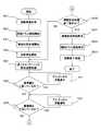
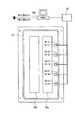
図1乃至図6は本発明の第一の実施形態に係る薄膜形成装置を説明した図であり、図1は第一の実施形態に係る薄膜形成装置を上面から見た部分断面図、図2は第一の実施形態に係る薄膜形成装置を側面から見た部分断面図、図3は図1の成膜プロセス領域周辺を拡大して示した説明図、図4は図1の矢視A方向から見たターゲットの正面図、図5は光ファイバの真空容器壁面への取付け状態を説明する斜視図、図6は第一の実施形態における成膜処理工程の流れを示すフローチャートである。 1 to 6 are views for explaining a thin film forming apparatus according to the first embodiment of the present invention. FIG. 1 is a partial sectional view of the thin film forming apparatus according to the first embodiment as viewed from above. FIG. 3 is a partial sectional view of the thin film forming apparatus according to the first embodiment as viewed from the side, FIG. 3 is an enlarged explanatory view showing the periphery of the film forming process region in FIG. 1, and FIG. FIG. 5 is a perspective view for explaining an attachment state of an optical fiber to a vacuum vessel wall surface, and FIG. 6 is a flowchart showing a flow of a film forming process in the first embodiment.
本実施形態では、スパッタの一例であるマグネトロンスパッタを行う薄膜形成装置を用いているが、スパッタの種類としてはこのようなマグネトロンスパッタに限定されるものでなく、マグネトロン放電を用いない2極スパッタ等の公知のスパッタを行う薄膜形成装置を用いることもできる。 In this embodiment, a thin film forming apparatus that performs magnetron sputtering, which is an example of sputtering, is used. However, the type of sputtering is not limited to such magnetron sputtering, and bipolar sputtering that does not use magnetron discharge or the like. A known thin film forming apparatus that performs sputtering can also be used.
本実施形態の薄膜形成装置では、目的の膜厚よりも薄い薄膜をスパッタ処理で作成したのちに、形成された薄膜に対してプラズマ処理を行う工程を繰り返すことで目的の膜厚を有する薄膜を基板上に形成する。本実施形態では、スパッタ処理とプラズマ処理によって平均0.01〜1.5nmの膜厚の薄膜を基板表面に形成する工程を回転ドラムの回転毎に繰り返すことで、目的とする数nm〜数百nm程度の膜厚の薄膜を形成している。 In the thin film forming apparatus of the present embodiment, a thin film having a target film thickness is formed by repeating a process of performing plasma processing on the formed thin film after forming a thin film having a thickness smaller than the target film thickness by sputtering. Form on the substrate. In the present embodiment, a process of forming a thin film having an average thickness of 0.01 to 1.5 nm on the substrate surface by sputtering treatment and plasma treatment is repeated for each rotation of the rotating drum, so that a desired number of nm to several hundreds. A thin film having a thickness of about nm is formed.
本実施形態の薄膜形成装置1は、図1乃至図4に示すように、真空容器11と、回転ドラム13と、モータ17と、スパッタ手段20Aと、プラズマ発生手段60Aとを主要な構成要素としている。 As shown in FIGS. 1 to 4, the thin
真空容器11は、公知の薄膜形成装置で通常用いられるようなステンレススチール製で、略直方体形状をした中空体である。真空容器11の内部は、図1に示すように、本発明の開閉扉としての扉11Cによって薄膜形成室11Aとロードロック室11Bに分けられる。真空容器11の上方には扉11Cを収容する扉収納容器(不図示)が接続されており、扉11Cは、真空容器11の内部と扉収納室の内部との間でスライドすることで開閉する。 The
真空容器11には、ロードロック室11Bと真空容器11の外部とを仕切る扉11Dが設けられている。扉11Dは、スライドまたは回動することで開閉する。真空容器11の内部の薄膜形成室11Aには、排気用の配管15aが接続され、この配管には真空容器11内を排気するための真空ポンプ15が接続されている。配管15aの開口は、真空容器11内の成膜プロセス領域20と反応プロセス領域60との間に位置しており、成膜プロセス領域で飛散した膜原料物質を真空ポンプ15で吸引することで、成膜プロセス領域20から飛散した膜原料物質が反応プロセス領域に侵入して基板表面やプラズマ発生手段を汚染することを防止している。
また、真空容器11の内部のロードロック室11Bには、排気用の配管15a'が接続され、この配管には真空容器11内を排気するための真空ポンプ15'が接続されている。The
Further, an
本実施形態の薄膜形成装置は、このようなロードロック室11Bを備えているため、薄膜形成室11A内の真空状態を保持した状態で基板の搬入出を行うことが可能となる。従って、基板を搬出する毎に真空容器内を脱気して真空状態にする手間を省くことが可能となり、高い作業効率で成膜処理を行うことができる。
なお、本実施形態の真空容器11は、ロードロック室を備えるロードロック方式を採用しているが、ロードロック室を設けないシングルチャンバ方式を採用することも可能である。また、複数の真空室を備え、それぞれの真空室で独立に薄膜形成を行うことが可能なマルチチャンバ方式を採用することも可能である。Since the thin film forming apparatus of the present embodiment includes such a
In addition, although the
回転ドラム13は、表面に薄膜を形成させる基板Sを真空容器11内で保持するための部材であり、本発明の基体保持手段に該当する。回転ドラム13は、複数の基板保持具13a,フレーム13b,締結具13cを主要な構成要素としている。基板保持具13aはステンレススチール製の平板状部材で、基板Sを保持するための複数の基板保持孔を板面の長手方向に沿って一列に備えている。基板Sは基板保持具13aの基板保持孔に収納され、脱落しないようにネジ部材等を用いて基板保持具13aに固定されている。また、基板保持具13aの長手方向における両端付近の板面にはネジ穴が設けられている。 The
フレーム13bはステンレススチール製の部材で、上下に配置された2つの環状部材から構成されている。フレーム13bの環状部材には、基板保持具のネジ穴と対向する位置にネジ穴が設けられている。基板保持具13aは、ボルトおよびナットからなる締結具13cを用いてフレーム13bに固定される。なお、本実施形態における回転ドラム13は、平板状の基板保持具13aを複数配置しているため、横断面が多角形をした多角柱状をしているが、回転ドラム13の形状はこのような多角柱状のものに限定されず、中空の円筒状や円錐状のものであってもよい。 The
基板Sは、本発明の基体に該当するものである。本実施形態では、基板Sはガラス製の円板状部材で、薄膜形成処理により表面に薄膜が形成される。基体としては本実施形態のような円板状のもの限定されず、レンズ状のものや管状のものなどを用いることもできる。また、基板Sの材質も本実施形態のようなガラス製に限定されず、プラスチックや金属等であってもよい。 The substrate S corresponds to the substrate of the present invention. In the present embodiment, the substrate S is a glass disk-like member, and a thin film is formed on the surface by a thin film forming process. The substrate is not limited to a disk-like one as in this embodiment, and a lens-like one or a tubular one can also be used. Further, the material of the substrate S is not limited to glass as in the present embodiment, and may be plastic or metal.
真空容器11内部に設置された回転ドラム13は、薄膜形成室11Aとロードロック室11Bの間を移動できるように構成されている。本実施形態では、真空容器11の底面にレール(不図示)が設置されており、回転ドラム13はこのレールに沿って移動する。回転ドラム13は、円筒の筒方向の中心軸線Z(図2参照)が真空容器11の上下方向になるように真空容器11内に配設される。基板保持具13aをフレーム13bに取り付ける際やフレーム13bから取り外す際には、回転ドラム13はロードロック室11B内で回転可能な状態にロックされている。一方、成膜中にあっては、回転ドラム13は薄膜形成室11A内で回転可能な状態にロックされる。 The
図2に示すように、回転ドラム13の下面中心部には、回転軸18aが回転ドラム13の中心軸線に沿って設けられている。回転軸18a表面の回転ドラム13と係合する面は、絶縁部材で構成されている。これにより、基板における異常放電を防止することが可能となる。
回転軸18aは真空容器11の下壁を貫通して真空容器11の外部へ延出している。回転軸18aの一端はモータ17の回転軸17aと係合する構造となっており、真空容器11の外部に設けられたモータ17の回転軸と係合している。
回転ドラム13は、真空容器11内の真空状態を維持した状態で、真空容器11の下部に設けられたモータ17を駆動させることによって中心軸線Zを中心に回転する。各基板Sは、回転ドラム13上に保持されているため、回転ドラム13が回転することで、中心軸線Zを公転軸として公転する。As shown in FIG. 2, a rotating
The
The
回転ドラム13の上面には、ドラム回転軸18bが回転ドラム13の中心軸線に沿って設けられており、回転ドラム13の回転に伴ってドラム回転軸18bも回転する。真空容器11の上壁には孔部が設けられており、ドラム回転軸17bはこの孔部を貫通して真空容器11の外部に通じている。孔部の内面には軸受が設けられており、回転ドラム13の回転をスムーズに行えるようにしている。また、真空容器11とドラム回転軸18bとの間は、Oリングで気密が保たれている。 On the upper surface of the
次に、基板Sの表面に薄膜を形成する成膜プロセス領域20と、反応プロセス領域60について説明する。真空容器11内壁には、回転ドラム13へ向けて仕切壁12,14が立設して設けられている。本実施形態における仕切壁12,14は、真空容器11と同じステンレススチール製の部材である。仕切壁12,14は、真空容器11の内壁面から回転ドラム13へ向けて四方を囲んだ状態で設けられている。 Next, the film forming
真空容器11の側壁は外方に突出した横断面凸状をしており、突出した側面にはスパッタ手段20Aが設けられている。成膜プロセス領域20は、真空容器11の内壁面,仕切壁12,回転ドラム13の外周面及びスパッタ手段20Aに囲繞された領域に形成されている。成膜プロセス領域20では基板Sの表面に薄膜を形成するスパッタ処理が行われる。
一方、成膜プロセス領域20から回転ドラム13の回転軸を中心として90°離間した真空容器11の側壁もまた、外方に突出した横断面凸状をしており、突出した側面にはプラズマ発生手段60Aが設けられている。反応プロセス領域60は、真空容器11の内壁面,仕切壁14,回転ドラム13の外周面及びプラズマ発生手段60Aに囲繞された領域に形成されている。反応プロセス領域60では、基板Sの表面に形成された薄膜に対してプラズマ処理が行われる。The side wall of the
On the other hand, the side wall of the
モータ17によって回転ドラム13が回転すると、回転ドラム13の外周面に保持された基板Sが公転して、成膜プロセス領域20に面する位置と反応プロセス領域60に面する位置との間を繰り返し移動することになる。そして、このように基板Sが公転することで、成膜プロセス領域20でのスパッタ処理と、反応プロセス領域60でのプラズマ処理とが順次繰り返し行われて、基板Sの表面に薄膜が形成される。 When the
(成膜プロセス領域)
以下に、本発明の成膜プロセス領域について説明する。図3に示すように、本発明の成膜プロセス領域20には、回転ドラム13の外周面に対向するように本発明のスパッタ手段20Aが設置されている。スパッタ手段20Aは、一対のマグネトロンスパッタ電極21a,21bと、トランス23を介して接続された交流電源24により構成される。真空容器11の壁面は外方に突出しており、この突出部にマグネトロンスパッタ電極21a,21bが側壁を貫通した状態で配置されている。このマグネトロンスパッタ電極21a,21bは、不図示の絶縁部材を介して接地電位にある真空容器11に固定されている。(Deposition process area)
Below, the film-forming process area | region of this invention is demonstrated. As shown in FIG. 3, the sputtering means 20 </ b> A of the present invention is installed in the film forming
マグネトロンスパッタ電極21a,21bは、複数の磁石が所定の方向に配置された構造を有している。マグネトロンスパッタ電極21a,21bは、トランス23を介して交流電源24に接続され、両電極に1k〜100kHzの交番電界が印加可能に構成されている。マグネトロンスパッタ電極21a,21bには、ターゲット22a,22bが夫々保持されている。図3に示すように、ターゲット22a,22bの形状は平板状であり、ターゲット22a,22bの表面が、回転ドラム13の中心軸線Zと垂直となるように保持される。 The
本例のターゲット22a,22bは、所定の面積を有するように膜原料物質を平板状に形成したものであり、回転ドラム13の側面に対向するようにマグネトロンスパッタ電極21a,21bに保持される。ターゲットの材質としては任意のもの、例えば、ケイ素,ニオブ,チタン,アルミニウム,ゲルマニウム等を採用することが可能である。また、ターゲットの形状としては、本実施形態のように平板状に限定されず、円板状や多角形平板状のものなど、任意の形状のものであってよい。 The
図3に示すように、成膜プロセス領域20周辺にはスパッタガス供給手段と反応性ガス供給手段の2種類のガス供給手段が設けられている。スパッタガス供給手段は、スパッタガスボンベ26と、複数の配管29a−1〜29a−5と、夫々の配管に設けられ,スパッタガスの流量を調整する複数のマスフローコントローラ25−1〜25−5と、を主要な構成要素として具備している。
また、反応性ガス供給手段は、反応性ガスボンベ28と、複数の配管29a−1〜29a−5と、夫々の配管に設けられ,反応性ガスの流量を調整する複数のマスフローコントローラ27−1〜27−5と、を主要な構成要素として具備している。
なお、配管29a−1〜29a−5は、本発明における供給路に該当する。As shown in FIG. 3, two types of gas supply means, a sputtering gas supply means and a reactive gas supply means, are provided around the film forming
The reactive gas supply means includes a
The
スパッタガスボンベ26,反応性ガスボンベ28,複数のマスフローコントローラ25,27はいずれも真空容器11外部に設けられている。本実施形態では、マスフローコントローラ25−1〜25−5と、27−1〜27−5の計10つのマスフローコントローラが設けられている。マスフローコントローラ25−1〜25−5は、不活性ガスとしてのアルゴンガスを貯留する単一のスパッタガスボンベ26に配管29cを介して夫々接続されている。また、マスフローコントローラ27−1〜27−5は、反応性ガスを貯留する単一の反応性ガスボンベ28に配管29dを介して夫々接続されている。
なお、マスフローコントローラ25は本発明におけるスパッタガス流量調整手段に該当し、マスフローコントローラ27は本発明における反応性ガス流量調整手段に該当する。The sputtering
The
マスフローコントローラ25−1とマスフローコントローラ27−1はY字型の配管29a−1で接続されており、配管29a−1の一端は真空容器11の側壁を貫通して成膜プロセス領域20のターゲット22bの側部に位置して導入口を形成している。同様に、マスフローコントローラ25−2〜25−5とマスフローコントローラ27−2〜27−5はY字型の配管29a−2〜29a−5で夫々接続されている。配管29a−2〜29a−5は夫々真空容器11の側壁を貫通して成膜プロセス領域20のターゲット22b側部に位置するように配設され、夫々単一の導入口29b−2〜29b−5を形成している。 The mass flow controller 25-1 and the mass flow controller 27-1 are connected by a Y-shaped pipe 29 a-1, and one end of the pipe 29 a-1 penetrates the side wall of the
図4に示すように、夫々の導入口29b−1〜29b−5は、ターゲット22bの側部上方から所定の距離を隔てて順に配置されている。配管29a−1を通じて供給されるガスは配管29a−1に設けられた導入口29b−1からターゲット22a,22bの前面に導入される。同様に、他の配管29aを通じて供給されるガスは、夫々の配管に形成された導入口29bからターゲット22a,22bの前面に供給される。
なお、本実施形態では、配管29aやマスフローコントローラ25,27は夫々5つずつ設けられているが、これらの部材の数としては5つに限定されず、任意の数を設定することが可能である。As shown in FIG. 4, the
In this embodiment, five
また、本実施形態では、スパッタガスをターゲットへ導入する配管と反応性ガスをターゲットへ導入する配管を共通にして、両ガスの混合ガスとしてターゲットへ導入する構成としているが、本発明の供給路としてはこのような共通としたものに限定されず、スパッタガス導入用の配管と反応性ガス導入用の配管を夫々別々に設けて、夫々のガスを別々にターゲットへ導入する構成としてもよい。 In the present embodiment, the piping for introducing the sputtering gas to the target and the piping for introducing the reactive gas to the target are made common, and the mixed gas of both gases is introduced to the target. However, the present invention is not limited to such a common configuration, and a pipe for introducing a sputtering gas and a pipe for introducing a reactive gas may be separately provided, and the respective gases may be separately introduced into the target.
マスフローコントローラはガスの流量を調節する装置であり、ガスボンベからのガスが流入する流入口と、ガスを真空容器11側へ流出させる流出口と、ガスの質量流量を検出するセンサと、ガスの流量を調整するコントロールバルブと、流入口より流入したガスの質量流量を検出するセンサと、センサにより検出された流量に基づいてコントロールバルブの制御を行う電子回路とを主要な構成要素として備えている。電子回路には外部から所望の流量を設定することが可能となっている。 The mass flow controller is a device that adjusts the flow rate of gas, an inlet port through which a gas from a gas cylinder flows in, an outlet port through which the gas flows out to the
流入口よりマスフローコントローラ内に送入されたガスの質量流量は、センサにより検出される。センサの下流にはコントロールバルブが設けられており、コントロールバルブは、センサで検出した流量と、設定された基準値とを比較し、ガスの流量が基準値に近づくようにコントロールバルブの開閉を行うことで、流量の制御を行う。 The mass flow rate of the gas sent into the mass flow controller from the inlet is detected by a sensor. A control valve is provided downstream of the sensor, and the control valve compares the flow rate detected by the sensor with a set reference value, and opens and closes the control valve so that the gas flow rate approaches the reference value. Thus, the flow rate is controlled.
スパッタガスボンベ26からの不活性ガスは、マスフローコントローラ25−1により流量を調節され、配管29a−1内に流入する。一方、スパッタガスボンベ26からの反応性ガスは、マスフローコントローラ27−1により流量を調節され、配管29a−1内に流入する。配管29a−1に流入した不活性ガス及び反応性ガスの混合ガスは、配管29a−1の導入口29b−1より成膜プロセス領域20に配置されたターゲット22a,22bの前面に導入される。同様に、マスフローコントローラ25−2〜25−5で流量を調整された不活性ガスと、マスフローコントローラ27−2〜27−5で流量を調整された反応性ガスの混合ガスは、他の配管29a−2〜29a−5の導入口29b−2〜29b−5より成膜プロセス領域20に夫々導入される。
不活性ガスとしては、例えばアルゴンやヘリウム等が挙げられる。また、反応性ガスとしては、例えば酸素ガス,窒素ガス,弗素ガス,オゾンガス等が挙げられる。The flow rate of the inert gas from the sputtering
Examples of the inert gas include argon and helium. Examples of the reactive gas include oxygen gas, nitrogen gas, fluorine gas, and ozone gas.
次に、本発明の供給量測定手段について説明する。本発明の薄膜形成装置1は、光ファイバ31−1〜31−5と、光学測定装置33と、膜厚制御装置100とを主要な構成要素として具備している。
なお、光ファイバ31−1〜31−5と、光学測定装置33は、本発明の供給量測定手段を構成する。また、光ファイバ31−1〜31−5は、本発明の受光部に該当する。更に、光学測定装置33は、本発明の光学測定部に該当する。Next, the supply amount measuring means of the present invention will be described. The thin
The optical fibers 31-1 to 31-5 and the
図3及び図4に示すように、ターゲット22a,22bを挟んで導入口29b−1〜29b−5に対向する位置には、本発明の供給量測定手段を構成する光ファイバ31−1〜31−5が受光面をプラズマP方向に向けて夫々設けられている。光ファイバ31−1〜31−5は、夫々真空容器11の側壁を貫通して真空容器11の外部へ延出している。光ファイバ31−1〜31−5は夫々光学測定手段としての光学測定装置33に接続されている。 As shown in FIGS. 3 and 4, optical fibers 31-1 to 31-31 constituting the supply amount measuring means of the present invention are located at positions facing the
なお、光ファイバ31−1〜31−5の受光面が配設される位置としては、上記のようなターゲット22a,22bを挟んで導入口に対向する位置に限定されない。例えば、導入口29b−1〜29b−5が配設された真空容器側面と同じ側面に、導入口29b−1〜29b−5と夫々隣接する位置に配置され、夫々の受光面がプラズマP方向に向くようにしてもよい。
すなわち、配管29a−1〜29a−5の夫々の導入口29b−1〜29b−5から導入されるガスによるプラズマPの発光を夫々観測可能であり、且つ、他の導入口から導入されるガスによる発光を極力観測しないような位置であればよい。The position where the light receiving surfaces of the optical fibers 31-1 to 31-5 are disposed is not limited to the position facing the introduction port with the
That is, the emission of the plasma P by the gas introduced from the
なお、光ファイバの数としては本実施形態のような5つに限定されず、所望の数を配設することが可能である。従って、光ファイバ31の数を多くすればするほど薄膜形成装置の製造にかかるコストや時間がかかるが、基板表面に形成される薄膜の膜厚分布をより精度よく測定することが可能となる。 The number of optical fibers is not limited to five as in the present embodiment, and a desired number can be arranged. Accordingly, as the number of
また、図4に示すように、真空容器11内部の光ファイバ31−1〜31−5の周囲には、光ファイバ31−1〜31−5を覆うようにカバー32−1〜32−5が夫々設けられており、光ファイバ31の端部が膜原料物質などにより汚染されることを防止している。 Further, as shown in FIG. 4, covers 32-1 to 32-5 are provided around the optical fibers 31-1 to 31-5 inside the
更に、図5に示すように、光ファイバ31−1〜31−5の端面とプラズマPとの間にはシャッター34−1〜34−5が夫々設けられていると好適である。シャッター34−1〜34−5は夫々支持棒35−1〜35−5に固定され、この支持棒は真空容器11の壁面を貫通して真空容器11の外部に設けられたモータ36の回転軸と接続されている。
後述するように、膜厚測定時にはモータ36を駆動してシャッター34−1〜34−5を移動させ(図5(a))、プラズマからの光が光ファイバの端面から入射するように位置させ、膜厚測定時以外にあっては光ファイバの端面とプラズマPとの間にシャッター34が位置するように移動して(図5(b))、プラズマから飛翔する膜原料物質が光ファイバの端面に付着しないようにしている。
なお、シャッター34−1〜34−5は、本発明の遮蔽部材に該当し、モータ36は本発明の遮蔽部材駆動手段に該当する。Furthermore, as shown in FIG. 5, it is preferable that shutters 34-1 to 34-5 are provided between the end faces of the optical fibers 31-1 to 31-5 and the plasma P, respectively. The shutters 34-1 to 34-5 are fixed to support rods 35-1 to 35-5, respectively, and the support rods penetrate the wall surface of the
As will be described later, when the film thickness is measured, the
The shutters 34-1 to 34-5 correspond to the shielding member of the present invention, and the
膜厚測定時において、光ファイバ31の端面からは後述するプラズマPからの光が入射し、入射した光は光ファイバ31の内部を伝送して光学測定装置33へ導出される。光学測定装置33は、光ファイバ31−1〜31−5から伝送された光を検知する装置である。光学測定装置33はコリメータと、グレイティングのような分光素子と、受光素子とを主要な構成要素として備えている(いずれも不図示)。 During film thickness measurement, light from plasma P, which will be described later, enters from the end face of the
光学測定装置33に入射した反射光はコリメータを通過する。コリメータは細いスリットが複数設けた平板状部材で、光ファイバから伝送された反射光を平行な光線の束にする。コリメータを通過した反射光はグレイティングに照射される。
グレイティングは回折格子を備え、コリメータから入射した光のうち所定の波長の光のみを出射する。グレイティングは回転軸を有しており、グレイティングに入射する光とグレイティングとの相対角度を変更することにより、出射する光の波長を変更することが可能となっている。グレイティングから出射した光は受光素子に照射される。The reflected light incident on the
The grating includes a diffraction grating and emits only light having a predetermined wavelength out of light incident from the collimator. The grating has a rotation axis, and the wavelength of the emitted light can be changed by changing the relative angle between the light incident on the grating and the grating. The light emitted from the grating is applied to the light receiving element.
受光素子としては、フォトダイオードが用いられている。フォトダイオードはp型及びn型の半導体を接合したもので、その接合面に光が当たると、その光の強度に応じた電流が発生する。この電流は光学測定装置33内のA−D変換器によりデジタル信号化されて出力される。
光学測定装置33は、膜厚制御装置100に電気的に接続されており、光学測定装置33から出力された電気信号は膜厚制御装置100に入力される。A photodiode is used as the light receiving element. A photodiode is a junction of p-type and n-type semiconductors. When light strikes the junction surface, a current corresponding to the intensity of the light is generated. This current is converted into a digital signal by an A / D converter in the
The
膜厚制御装置100は、演算手段としてのCPUと、記憶手段としてのハードディスク及び半導体メモリと、入力手段としてのキーボード及びマウスと、出力手段としてのディスプレイと、複数の入力端子と、複数の出力端子と、を備える。光学測定装置33から出力されたデジタル信号は、膜厚制御装置100の入力端子から膜厚制御装置100へ入力される。膜厚制御装置100の出力端子からは導線が導出され、マスフローコントローラ25−1〜25−5及び27−1〜27−5に電気的に接続されている。 The film
光学測定装置33から膜厚制御装置100に入力された発光強度に関する信号は、膜厚制御装置100内部のCPUにより処理され、膜厚に関する情報としてメモリやハードディスクに保存される。
一方、膜厚制御装置100は、マスフローコントローラ25,27の設定流量を変更することが可能となっている。すなわち、膜厚制御装置100のメモリには、マスフローコントローラ25,27を通過するガスの流量についての設定値が記憶されており、膜厚制御装置100は、マスフローコントローラ25,27と電気的に接続されてされ、マスフローコントローラ25,27を通過するガスの流量を変更することが可能となっている。A signal relating to the emission intensity input from the
On the other hand, the
膜厚制御装置100からの設定流量の変更を指示する電気信号が発生した場合、この電気信号はメモリに記憶された流量値とともに膜厚制御装置100の出力端子からケーブルを通じてマスフローコントローラ25,27に伝送され、マスフローコントローラ25,27の夫々の電気回路に保持された設定流量を膜厚制御装置100から指示された流量値に夫々書き換えることにより、設定流量を変更することが可能となる。これにより、膜厚制御装置100は、スパッタガスボンベ26、反応性ガスボンベ28から配管29aを介して成膜プロセス領域20に流入するガスの流量を調整することが可能となっている。 When an electrical signal for instructing a change in the set flow rate from the film
続いて、本実施形態の膜厚制御装置100を用いて基板Sの表面に形成される薄膜の膜厚を測定し、この膜厚分布に基づいて薄膜形成工程を制御する方法について説明する。本実施形態では、ターゲット22a,22bとしてケイ素、不活性ガスとしてアルゴン、反応性ガスとして酸素を用いた例について説明する。 Next, a method for measuring the film thickness of the thin film formed on the surface of the substrate S using the film
成膜プロセス領域20にアルゴンガスが供給されて、ターゲット22a,22bの周辺が不活性ガス雰囲気になった状態で、マグネトロンスパッタ電極21a,21bに交流電源24から交番電極が印加されると、ターゲット22周辺のアルゴンガスの一部は電子を放出してイオン化する。マグネトロンスパッタ電極21a,21bに配置された磁石によりターゲット22a、22bの表面に漏洩磁界が形成されるため、この電子はターゲット表面近傍に発生した磁界中を、トロイダル曲線を描きながら周回する。この電子の軌道に沿って強いプラズマが発生し、このプラズマに向けてアルゴンガスのイオンが加速され、ターゲット22に衝突することでターゲット表面のケイ素原子(Si)が叩き出される。このケイ素原子の一部は反応ガスである酸素によりプラズマ中で酸化されて酸化ケイ素(SiO)に変換される。これらのケイ素原子、酸化ケイ素は膜原料物質として基板Sの表面に付着して薄膜を形成する。 When an alternating electrode is applied from the
プラズマ中ではケイ素原子,酸化ケイ素やアルゴンは気体状態として存在している。電極の放電により励起された気体は、そのエネルギーの一部を光として放出している。この光は物質の種類により異なる発光スペクトルを有しており、この発光スペクトルはその気体に特徴的なピーク波長を有している。例えば、ケイ素原子による光のピーク波長は288nm、酸化ケイ素の中の酸素とケイ素の結合(SiO)の場合は424nm、アルゴンの場合は750nmとなっている。 In the plasma, silicon atoms, silicon oxide and argon are present in a gaseous state. The gas excited by the discharge of the electrode emits part of its energy as light. This light has an emission spectrum that varies depending on the type of substance, and this emission spectrum has a peak wavelength characteristic of the gas. For example, the peak wavelength of light due to silicon atoms is 288 nm, 424 nm for the bond between oxygen and silicon (SiO) in silicon oxide, and 750 nm for argon.
本実施形態の薄膜形成装置では、この特徴ピークを示す波長における光の強度を測定することで、所定の物質の発光強度を測定しているが、測定する波長については特徴ピークを示す波長と同一のものに限定されず、特徴ピークを示す波長以外であっても、特定の物質と他の物質を識別可能な波長であれば測定波長とすることが可能である。具体的には、酸化ケイ素(SiO)の特徴ピークは424nmであるが、400nm〜450nmの範囲であっても他の物質と十分識別可能であるため、測定波長とすることができる。 In the thin film forming apparatus of the present embodiment, the light emission intensity of a predetermined substance is measured by measuring the intensity of light at a wavelength exhibiting the characteristic peak. The wavelength to be measured is the same as the wavelength exhibiting the characteristic peak. However, the wavelength is not limited to a wavelength that exhibits a characteristic peak, but can be a measurement wavelength as long as it is a wavelength that can distinguish a specific substance from another substance. Specifically, the characteristic peak of silicon oxide (SiO) is 424 nm, but even if it is in the range of 400 nm to 450 nm, it can be sufficiently distinguished from other substances, so that it can be a measurement wavelength.
特定の波長における光の強度はプラズマ中に含まれる物質の量を反映しており、プラズマ中に含まれる物質の量は、基板表面に付着する膜原料物質の量と相関している。すなわち、例えばプラズマ中に含まれるケイ素原子の発光強度が大きくなるほどプラズマ中に含まれるケイ素原子の量が多くなり、基板表面に付着するケイ素原子の量が多くなる。同様に、プラズマ中に含まれる酸化ケイ素(SiO)の発光強度が大きくなるほどプラズマ中に含まれる酸化ケイ素の量が多くなり、基板表面に付着する酸化ケイ素の量が多くなる。 The intensity of light at a specific wavelength reflects the amount of substance contained in the plasma, and the amount of substance contained in the plasma correlates with the amount of film raw material adhering to the substrate surface. That is, for example, as the emission intensity of silicon atoms contained in plasma increases, the amount of silicon atoms contained in the plasma increases, and the amount of silicon atoms attached to the substrate surface increases. Similarly, as the emission intensity of silicon oxide (SiO) contained in the plasma increases, the amount of silicon oxide contained in the plasma increases, and the amount of silicon oxide attached to the substrate surface increases.
また、プラズマ中に含まれるアルゴンガスの発光強度が大きくなるほど、プラズマ中に含まれるアルゴンの量が多くなる。プラズマ中に含まれるアルゴンの量が多いと、スパッタによりターゲットに衝突するアルゴン原子の数が増加するため、スパッタによりターゲットから叩き出されるケイ素原子の数が多くなる。この結果、基板表面に付着する膜原料物質の量が多くなる。 Further, as the emission intensity of the argon gas contained in the plasma increases, the amount of argon contained in the plasma increases. If the amount of argon contained in the plasma is large, the number of argon atoms that collide with the target due to sputtering increases, so that the number of silicon atoms knocked out of the target by sputtering increases. As a result, the amount of film raw material adhering to the substrate surface increases.
プラズマPの周辺には光ファイバ31−1〜31−5が配置されており、プラズマPにおいて発光する光を光学測定装置33へ伝送する。光学測定装置33では、所定の波長についてプラズマP中の光の強度が計測される。光ファイバ31−1〜31−5はプラズマPの周辺に所定の距離を隔てて配設されているため、プラズマP中の気体の密度分布は、光ファイバ31−1〜31−5で計測される光の強度に反映される。また、基板Sの表面に形成される最終薄膜の膜厚に反映される。すなわち、プラズマP中のケイ素原子の強度が大きい程、基板Sの表面に形成される薄膜のケイ素原子含有量が多くなる。同様に、酸化ケイ素(SiO)の強度が大きくなると、基板Sの表面に形成される薄膜の酸化ケイ素(SiO)含有量が多くなる。 Optical fibers 31-1 to 31-5 are arranged around the plasma P, and transmit light emitted from the plasma P to the
膜厚制御装置100は、光学測定装置33で観測された光の強度に基づいて、マスフローコントローラ25,27を用いて成膜プロセス領域20に導入されるガスの流量を調整することにより成膜レートを調整する。成膜レートは、所定の基準値を設定して、この基準値に合うようにマスフローコントローラ25,27を制御することにより調整している。具体的には、光ファイバ31−1を通じて観測されたケイ素原子(Si)の特徴ピークでの波長における発光強度が基準値よりも下回っている場合、光学測定装置33はマスフローコントローラ25の電子回路に格納された流量の設定値を変更して、配管29−1に導入されるアルゴンガスの流量を大きくすることにより成膜レートを上昇させる。 The film
また、光ファイバ31−1を通じて観測された酸化ケイ素(SiO)とケイ素原子(Si)の発光強度の比を算出して、これがすべての光ファイバ31−1〜31−5でほぼ等しくなるように制御してもよい。 Further, the ratio of the emission intensity of silicon oxide (SiO) and silicon atom (Si) observed through the optical fiber 31-1 is calculated so that it is substantially equal in all the optical fibers 31-1 to 31-5. You may control.
後述するように、成膜プロセス領域20で基板表面に付着した膜原料物質は、反応プロセス領域60においてプラズマ処理されて完全に酸化される。ここで、ターゲットを構成する物質であるケイ素原子(Si)が酸化されて酸化物である酸化ケイ素(SiO)になると、体積の膨張が起こる。
従って、成膜プロセス領域20で形成される薄膜中のケイ素原子(Si)と酸化ケイ素(SiO)の比を各基板や基板表面のあらゆる位置においてほぼ等しくすることで、最終薄膜が形成された後においても均一な膜厚を有する薄膜を得ることが可能となる。As will be described later, the film raw material adhering to the substrate surface in the film forming
Therefore, after the final thin film is formed by making the ratio of silicon atoms (Si) and silicon oxide (SiO) in the thin film formed in the film forming
ここで、これらの比を調整する方法について具体的に説明する。ケイ素原子(Si)と酸化ケイ素(SiO)の比(SiO/Si)が一定になるように予め目標値を設定しておく。各光ファイバ31−1〜31−5で取得したプラズマ中のケイ素原子(Si)と酸化ケイ素(SiO)の発光強度の比(SiO/Si)が目標値よりも小さくなると、酸化ケイ素(SiO)の量が少ないと判断して、マスフローコントローラ27−1〜27−5を夫々制御して、配管29a−1〜29a−5を夫々通過する酸素ガスの流量を多くするように膜厚制御装置100で制御する。逆に、SiO/Siが目標値よりも大きくなると、マスフローコントローラ27−1〜27−5を夫々制御して、配管29a−1〜29a−5を夫々通過する酸素ガスの流量を少なくするように膜厚制御装置100で制御する。 Here, a method for adjusting these ratios will be described in detail. A target value is set in advance so that the ratio (SiO / Si) of silicon atoms (Si) to silicon oxide (SiO) is constant. When the ratio (SiO / Si) of the emission intensity of silicon atoms (Si) and silicon oxide (SiO) in the plasma obtained by each of the optical fibers 31-1 to 31-5 is smaller than the target value, silicon oxide (SiO) The
上述の膜厚調整方法では、単に光ファイバ31−1〜31−5で受光した発光強度に基づいて膜厚調整を行っているが、光学測定装置33で取得した発光強度を所定時間毎に加算して積分値を算出し、この積分値に基づいて膜厚制御装置100で配管29a−1〜29a−5を通過するガスの流量を調整することにより、膜厚の調節を行ってもよい。 In the above-described film thickness adjustment method, the film thickness is adjusted simply based on the light emission intensity received by the optical fibers 31-1 to 31-5, but the light emission intensity acquired by the
すなわち、発光強度はプラズマ中に含まれる物質の密度を反映しており、この密度が大きいほど基板表面に付着する膜原料物質の量が増加するという相関関係がある。従って、発光強度の積分値は、反応開始から測定時まで膜厚に堆積した膜原料物質の量、すなわち薄膜表面に堆積している薄膜の膜厚を反映している。このため、発光強度の積分値に基づいて膜厚制御を行うことは、実際に形成された薄膜の膜厚を間接的に反映する情報に基づいて膜厚制御を行うこととなり、最終膜厚を厳密に調整することが可能となる。 That is, the emission intensity reflects the density of the substance contained in the plasma, and there is a correlation that the larger the density, the greater the amount of film raw material adhering to the substrate surface. Therefore, the integrated value of the emission intensity reflects the amount of film raw material deposited on the film thickness from the start of the reaction to the measurement, that is, the film thickness of the thin film deposited on the thin film surface. For this reason, performing film thickness control based on the integral value of the emission intensity performs film thickness control based on information that indirectly reflects the film thickness of the actually formed thin film, and the final film thickness It becomes possible to adjust precisely.
具体的には、光学測定装置33に演算手段としてのCPUと、記憶手段としてのメモリを備え、光ファイバにより受光した光の発光強度の積分値を算出する。すなわち、CPUは、測定した発光強度とCPUによる内部クロックに基づいて、所定時間毎に発光強度を加算した値、すなわち発光強度の積分値を所定時間毎に算出する。発光強度の積分値は、膜厚に関する情報として膜厚制御装置100へ伝送される。
あるいは、光学測定装置33から伝送される発光強度に基づいて薄膜形成装置100のCPUで積分値を演算してもよい。Specifically, the
Alternatively, the integrated value may be calculated by the CPU of the thin
このように、発光強度の積分値に基づいて膜厚を調整する方法では、積分値を演算するため処理に要する時間が長くなるが、発光強度の積分値という基板表面に形成される実際の膜厚を反映した情報に基づいて膜厚を調整することが可能となるため、単に光の強度を一致させるように制御する方法と比較して、より正確に最終膜厚を制御して所望の膜厚を有する光学製品を得ることが可能となる。
一方、発光強度がほぼ等しくなるように膜厚を制御する方法では、積分値を演算するという工程を省略することができるため、処理に要する時間を短縮することが可能となる。As described above, in the method of adjusting the film thickness based on the integral value of the emission intensity, the time required for the process for calculating the integral value becomes long, but the actual film formed on the substrate surface called the integral value of the emission intensity. Since the film thickness can be adjusted based on the information reflecting the thickness, the final film thickness is controlled more accurately than the method of simply controlling the light intensities to coincide with each other. An optical product having a thickness can be obtained.
On the other hand, in the method of controlling the film thickness so that the light emission intensities are substantially equal, the step of calculating the integral value can be omitted, so that the time required for processing can be shortened.
(反応プロセス領域60)
続いて、反応プロセス領域60について説明する。前述したように、反応プロセス領域60では、成膜プロセス領域20で基板表面に形成された膜原料物質を酸化して、完全酸化物の生成を行っている。(Reaction process area 60)
Subsequently, the
反応プロセス領域60に対応する真空容器11の壁面には、プラズマ発生手段60Aを設置するための開口11aが形成されている。また、反応プロセス領域60には、マスフローコントローラ66を介して反応性ガスボンベ67内の反応性ガスを導入するための配管68が接続されている。 On the wall surface of the
仕切壁14の反応プロセス領域60に面する壁面には、熱分解窒化硼素(Pyrolytic Boron Nitride)からなる保護層(不図示)が被覆されている。さらに、真空容器11の内壁面の反応プロセス領域60に面する部分にも熱分解窒化硼素からなる保護層が被覆されている。熱分解窒化硼素は、化学的気相成長法(Chemical Vapor Deposition)を利用した熱分解法によって仕切壁14や真空容器11の内壁面へ被覆される。 The wall surface of the
プラズマ発生手段60Aは、反応プロセス領域60に面して設けられている。本実施形態のプラズマ発生手段60Aは、ケース体61と,誘電体板62と,アンテナ63と,マッチングボックス64と,高周波電源65と,真空ポンプ15とを有して構成されている。 The plasma generating means 60 </ b> A is provided facing the
ケース体61は、真空容器11の壁面に形成された開口11aを塞ぐ形状を備え、ボルト(不図示)で真空容器11の開口11aを塞ぐように固定されている。ケース体61が真空容器11の壁面に固定されることで、プラズマ発生手段60Aは真空容器11の壁面に取り付けられている。本実施形態において、ケース体61はステンレスで形成されている。 The
誘電体板62は、板状の誘電体で形成されている。本実施形態において、誘電体板62は石英で形成されているが、誘電体板62の材質としてはこのような石英だけではなく、Al2O3等のセラミックス材料で形成されたものでもよい。誘電体板62は、図示しない固定枠でケース体61に固定されている。誘電体板62がケース体61に固定されることで、ケース体61と誘電体板62によって囲繞された領域にアンテナ収容室61Aが形成されている。The
ケース体61に固定された誘電体板62は、開口11aを介して真空容器11の内部(反応プロセス領域60)に臨んで設けられている。このとき、アンテナ収容室61Aは、真空容器11の内部と分離している。すなわち、アンテナ収容室61Aと真空容器11の内部とは、誘電体板62で仕切られた状態で独立した空間を形成している。また、アンテナ収容室61Aと真空容器11の外部は、ケース体61で仕切られた状態で独立の空間を形成している。本実施形態では、このように独立の空間として形成されたアンテナ収容室61Aの中に、アンテナ63が設置されている。なお、アンテナ収容室61Aと真空容器11内部、アンテナ収容室61Aと真空容器11外部との間は、それぞれOリングで気密が保たれている。 The
本実施形態では、アンテナ収容室61Aの内部を排気して真空状態にするために、アンテナ収容室61Aに排気用の配管15aが接続されている。配管15aには、真空ポンプ15が接続されている。また、本実施形態において、配管15aは真空容器11の内部へも連通している。 In the present embodiment, an
配管15aには、真空ポンプ15から真空容器11の内部に連通する位置にバルブV1、V2が設けられている。また、配管15aには、真空ポンプ15からアンテナ収容室61Aの内部に連通する位置にバルブV1、V3が設けられている。バルブV2,V3のいずれかを閉じることで、アンテナ収容室61Aの内部と真空容器11の内部との間での気体の移動は阻止される。真空容器11の内部の圧力や、アンテナ収容室61Aの内部の圧力は、真空計(不図示)で測定される。Valves V <b> 1 and V <b> 2 are provided in the
本実施形態では、薄膜形成装置1に制御装置(不図示)を備えている。この制御装置には、真空計の出力が入力される。制御装置は、入力された真空計の測定値に基づいて、真空ポンプ15による排気を制御して、真空容器11の内部やアンテナ収容室61Aの内部の真空度を調整する機能を備える。本実施形態では、制御装置がバルブV1,V2,V3の開閉を制御することで、真空容器11の内部とアンテナ収容室61Aの内部を同時に、又は独立して排気できる。 In the present embodiment, the thin
アンテナ63は、高周波電源65から電力の供給を受けて、真空容器11の内部(反応プロセス領域60)に誘導電界を発生させ、反応プロセス領域60にプラズマを発生させるためのものである。本実施形態のアンテナ63は、銅で形成された円管状の本体部と、本体部の表面を被覆する銀で形成された被覆層を備えている。アンテナ63のインピーダンスを低下するためには、電気抵抗の低い材料でアンテナ63を形成するのが好ましい。そこで、高周波の電流がアンテナの表面に集中するという特性を利用して、アンテナ63の本体部を安価で加工が容易な、しかも電気抵抗も低い銅で円管状に形成し、アンテナ63の表面を銅よりも電気抵抗の低い銀で被覆している。このように構成することで、高周波に対するアンテナ63のインピーダンスを低減して、アンテナ63に電流を効率よく流して、プラズマを発生させる効率を高めている。 The
アンテナ63は、マッチング回路を収容するマッチングボックス64を介して高周波電源65に接続されている。マッチングボックス64内には、図示しない可変コンデンサが設けられている。
アンテナ63は、導線部を介してマッチングボックス64に接続されている。導線部はアンテナ63と同様の素材からなる。ケース体61には、導線部を挿通するための挿通孔が形成されており、アンテナ収容室61A内側のアンテナ63と、アンテナ収容室61A外側のマッチングボックス64とは、挿通孔に挿通される導線部を介して接続される。導線部と挿通孔との間にはシール部材が設けられ、アンテナ収容室61Aの内外で気密が保たれる。The
The
図1に示すように、反応プロセス領域60内には反応性ガス供給手段が設けられている。反応性ガス供給手段は、反応性ガスボンベ67と、反応性ガスの流量を調整するマスフローコントローラ66と、反応性ガスを反応プロセス領域60に導入する配管68を主要な構成要素として具備している。反応プロセス領域60の反応性ガスボンベ67,マスフローコントローラ66は、成膜プロセス領域20の反応性ガスボンベ28、マスフローコントローラ27と同様の装置を採用することが可能である。また、反応性ガスとして、成膜プロセス領域と同様に、酸素ガスなど公知のガスを採用することができる。 As shown in FIG. 1, reactive gas supply means is provided in the
反応性ガスボンベ67から配管68を通じて反応性ガスが反応プロセス領域60に導入された状態で、アンテナ63に高周波電源65から電力が供給されると、反応プロセス領域60内のアンテナ63に面した領域にプラズマPが発生する。このプラズマPからは電子が放出され、この電子により基板Sの表面に形成された薄膜中の金属原子やこの金属原子の不完全酸化物は酸化され、金属原子の完全酸化物となる。 When power is supplied to the
以下に、上述の薄膜形成装置1を用いて薄膜を製造する方法について、二酸化ケイ素(SiO2)を積層させた薄膜を製造する場合を例として説明する。図6は本実施形態における成膜処理工程の流れを示すフロー図である。薄膜の形成は、成膜の準備を行う工程、酸化ケイ素の薄膜を形成する工程、成膜を終了する工程の順に行われる。Hereinafter, a method for manufacturing the thin film using the thin
ステップ1(SA1)は、成膜準備処理を開始するステップである。まず、ターゲット22a,22bをマグネトロンスパッタ電極21a,21bに保持させる。ターゲット22a,22bの材料としてケイ素(Si)を用いる。扉11Cを閉じて、真空ポンプ15を作動させて排気を行い、薄膜形成室11Aを10−2Pa〜10Pa程度の真空状態にする。このとき、バルブV1,V2,V3が開放され、アンテナ収容室61Aも同時に排気される。Step 1 (SA1) is a step for starting the film forming preparation process. First, the
その後、回転ドラム13をロードロック室11Bの位置でロックした状態で、回転ドラム13に基板Sを保持した基板保持具13aを取り付ける。続いて、扉11Cを閉じた状態で、真空ポンプ15'を作動させてロードロック室11Bを排気して、10−2Pa〜10Pa程度の真空状態にする。更に、扉11Cを開いて、回転ドラム13を薄膜形成室11Aへ移動させる。回転ドラム13を薄膜形成室11Aへ移動させた後に、扉11Cを再び閉じる。真空容器11の内部,アンテナ収容室61Aの内部を上述の所定の圧力に減圧する。その後、真空容器11の内部,アンテナ収容室61Aの内部の圧力が安定した後に、成膜プロセス領域20の圧力を、1.0×10⁻¹Pa〜1.3Paに調整する。Thereafter, the
ステップ2(SA2)は、回転ドラム13の回転を開始するステップである。回転ドラム13の回転は、薄膜形成装置1の操作パネル(不図示)に設けられたドラム回転スイッチをオペレータが押すことにより開始される。ドラム回転スイッチを押下するとモータ17が作動し、回転ドラム13が回転する。 Step 2 (SA2) is a step for starting the rotation of the
本実施形態における成膜装置では、成膜プロセス領域20において基板Sの表面に中間薄膜を形成し、続く反応プロセス領域60においてこの中間薄膜の酸化処理を行って酸化後中間薄膜を形成している。このため、回転ドラム13の回転が遅いと、成膜プロセス領域20において形成される中間薄膜が厚くなり、反応プロセス領域60でこれを完全には酸化することができず、不純物の混じった不均一な最終薄膜が形成されるという問題がある。 In the film forming apparatus according to the present embodiment, an intermediate thin film is formed on the surface of the substrate S in the film forming
また、反応プロセス領域60において行われる酸化工程では、薄膜の酸化反応により薄膜の膨張現象が起こる。このような体積の増加は薄膜内部に圧縮応力を生じる。中間薄膜が厚い場合、生成される膜は中間薄膜間の隙間構造が少なく、酸化ケイ素が密に凝集した薄膜構造となっている。このような膜では、酸化反応による体積膨張の影響が大きい。一方、中間薄膜が薄い場合、生成される膜は中間薄膜間に生じる隙間構造を多く有している。このような膜において体積が膨張した場合、増加した体積は隙間構造に吸収されるため、膜内部に圧縮応力が生じにくい。 In the oxidation process performed in the
更に、回転ドラム13が低速回転している場合は、回転のぶれが大きく、正確な膜厚測定や成膜処理の制御が困難となる。一方、回転ドラム13の回転速度が大きい場合、回転軸の回転部分に発生する遠心力が大きく、ぶれの少ない安定した回転が得られる。 Further, when the
上述のように、回転ドラム13の回転速度が小さい場合、様々な問題が生じる。このような問題を回避するため、成膜処理において、回転ドラム13の回転速度は早いほうが好ましく、特に、20rpm以上であることが好適である。 As described above, various problems arise when the rotational speed of the
ステップ3(SA3)は、薄膜形成処理を開始するステップである。薄膜形成処理は、成膜プロセス領域20および反応プロセス領域60で行われる。成膜プロセス領域20では、ターゲット22a,22bに対してスパッタを行い、基板S表面にケイ素原子(Si)や酸化ケイ素(SiO)等から構成される中間薄膜が形成される。続く反応プロセス領域60では、成膜プロセス領域20で形成された中間薄膜に対して酸化処理を行うことにより、二酸化ケイ素(SiO2)を主成分とする酸化後中間薄膜が形成される。Step 3 (SA3) is a step for starting the thin film forming process. The thin film forming process is performed in the film forming
薄膜形成工程は、薄膜形成装置1に設けられた開始スイッチをオペレータが手動で操作することにより開始される。薄膜形成処理の開始指示により、交流電源24および高周波電源65から、それぞれトランス23およびマッチングボックス64に交流電圧が印加される。 The thin film forming process is started when an operator manually operates a start switch provided in the thin
スパッタ開始指示によりターゲット22a,22bに交番電界が印加されるようになると、ターゲット22a,22bが交互にアノードとカソードになり、成膜プロセス領域20でプラズマが形成される。このプラズマによってカソード上のターゲットに対してスパッタが行われる。 When an alternating electric field is applied to the
続いて基板Sは、回転ドラム13の回転に伴って、成膜プロセス領域20に面する位置から反応プロセス領域60に面する位置に移動する。反応プロセス領域60には、反応性ガスボンベ67から反応性ガスとして酸素ガスが導入される。 Subsequently, the substrate S moves from the position facing the film forming
次に、高周波電源65からアンテナ63に対して13.56MHzの交流電流が印加される。これにより、プラズマ発生手段60Aによって反応プロセス領域60にプラズマが発生する。反応プロセス領域60の圧力は、0.7×10⁻¹〜1.0Paに維持する。また、少なくとも反応プロセス領域60にプラズマを発生させている間は、アンテナ収容室61Aの内部の圧力は、10−3Pa以下を保持する。Next, an alternating current of 13.56 MHz is applied from the high
そして、回転ドラム13が回転して、ケイ素原子(Si)や酸化ケイ素(SiO)を含む中間薄膜が形成された基板Sが反応プロセス領域60に面する位置に搬送されてくると、反応プロセス領域60では、中間薄膜を構成するケイ素原子(Si)に対してプラズマ処理に完全に酸化する工程が行われる。すなわち、プラズマ発生手段60Aによって反応プロセス領域60に発生させたプラズマでケイ素(Si)や酸化ケイ素(SiO)を酸化反応させて、所望の組成の二酸化ケイ素(SiO2)に変換させる。これにより、薄膜中の物質の組成が変化する膜組成変換工程が行われる。When the
この反応プロセス領域60における膜組成変換工程では、酸化後の中間薄膜の膜厚が酸化前の中間薄膜の膜厚よりも厚くなるように、酸化後中間薄膜を形成する。すなわち、中間薄膜を構成するケイ素原子(Si)を所望の組成の二酸化ケイ素(SiO2)に変換することにより中間薄膜を膨張させ、酸化後の中間薄膜の膜厚を酸化前の中間薄膜の膜厚よりも厚くする。以下、成膜プロセス領域20でのスパッタ処理と、反応プロセス領域60での酸化処理を繰り返すことで、基板表面に最終薄膜が形成される。薄膜は回転ドラム13が回転するたびに積層されてゆく。In the film composition conversion step in the
ステップ4(SA4)は、光学測定を開始するステップである。光学測定を開始するには、まず光ファイバ31−1〜31−5の受光面とプラズマPの間に設けられたシャッター34−1〜34−5を、モータ36を駆動させることで移動させて、プラズマPからの光を受光面にて受光できるようにする。 Step 4 (SA4) is a step of starting optical measurement. To start the optical measurement, first, the shutters 34-1 to 34-5 provided between the light receiving surfaces of the optical fibers 31-1 to 31-5 and the plasma P are moved by driving the
ステップ5(SA5)は、光ファイバ31−1〜31−5{図6中では、31−n(nは1から5の整数)と記載}でプラズマPからの発光強度を取得する工程である。光ファイバ31−1〜31−5を伝送した光は、光学測定装置33でケイ素原子(Si)の特徴ピークを示す波長288nmについて光の強度が取得される。取得された光の強度に関する情報は、膜厚制御装置100に送信される。 Step 5 (SA5) is a step of acquiring the emission intensity from the plasma P in the optical fibers 31-1 to 31-5 {denoted as 31-n (where n is an integer from 1 to 5) in FIG. 6}. . The intensity of the light transmitted through the optical fibers 31-1 to 31-5 is acquired at a wavelength of 288 nm indicating the characteristic peak of silicon atoms (Si) by the
ステップ6(SA6)は、ステップ5で取得された光の強度が所定の基準値を上回っているかどうかを膜厚制御装置100で判断するステップである。基準値としては、前述のように事前にオペレータが設定してもよいし、各光ファイバ31−1〜31−5で取得された強度の平均値を算出して、これを基準値としてもよい。
光の強度が基準値を上回っている場合はステップ7に進む。上回っていない場合はステップ8に移行する。Step 6 (SA6) is a step in which the
If the light intensity exceeds the reference value, the process proceeds to step 7. If not, the process proceeds to step 8.
ステップ7(SA7)は、成膜プロセス領域20に導入されるアルゴンガスの流量を減少させるステップである。光ファイバ31−1〜31−5で取得された光の強度が基準値を上回っている場合には、マスフローコントローラ25−1〜25−5を制御して、配管29a−1〜29−5に導入されるアルゴンガスの流量を減少させる。これにより、成膜プロセス領域20に導入されるアルゴンガスの量が少なくなり、プラズマPからの光の強度が減少する。 Step 7 (SA7) is a step of decreasing the flow rate of the argon gas introduced into the film forming
ステップ8(SA8)は、ステップ5で取得された光の強度が所定の基準値を下回っているかどうかを膜厚制御装置100で判断するステップである。
光の強度が基準値を下回っている場合は、ステップ9に進む。下回っていない場合は、ステップ10に移行する。Step 8 (SA8) is a step in which the
If the light intensity is below the reference value, go to Step 9. If not, the process proceeds to step 10.
ステップ9(SA9)は、成膜プロセス領域20に導入されるアルゴンガスの流量を増加させるステップである。光ファイバ31−1〜31−5で取得された光の強度が基準値を下回っている場合には、マスフローコントローラ25−1〜25−5を制御して、配管29a−1〜29a−5に導入されるアルゴンガスの流量を増加させる。これにより、成膜プロセス領域20に導入されるアルゴンガスの量が多くなり、プラズマPからの光の強度が増加する。 Step 9 (SA9) is a step of increasing the flow rate of the argon gas introduced into the film forming
ステップ10(SA10)は、薄膜形成処理の終了条件になったかどうかを判断するステップである。薄膜形成処理が予め設定された条件になった場合に、所望の膜厚を有する薄膜が基板Sの表面に形成されたものとして、薄膜形成処理を終了する。ここで、薄膜形成処理の終了条件とは、例えば所定の時間が経過した場合や、所定の回転数だけ回転ドラム13が回転した場合、光ファイバ31−nで取得した光の強度の積分値が所定の条件になった場合などが挙げられる。この結果、終了条件になっていれば、ステップ11に移行する。終了条件になっていない場合は、再び光学測定を行って、所定の終了条件になるまで薄膜形成工程を継続する。 Step 10 (SA10) is a step of determining whether or not the end condition of the thin film forming process has been reached. When the thin film forming process is in a preset condition, it is assumed that a thin film having a desired film thickness is formed on the surface of the substrate S, and the thin film forming process is terminated. Here, the end condition of the thin film forming process is, for example, when the predetermined time has elapsed or when the
ステップ11(SA11)は、薄膜形成工程の停止を行うステップである。薄膜形成工程を停止するには、薄膜形成装置1に設けられた制御装置により自動的に行ったり、オペレータが手動で停止操作を行ったりするなどの方法がある。 Step 11 (SA11) is a step of stopping the thin film forming process. In order to stop the thin film forming process, there are a method in which it is automatically performed by a control device provided in the thin
薄膜形成工程の停止指示を受けた薄膜形成装置1は、交流電源24からトランス23への電力の供給を停止する。また、高周波電源65から、マッチングボックス64への電力の供給を停止する。これにより、成膜プロセス領域20での成膜処理と、反応プロセス領域60での酸化処理の両方の処理が停止し、薄膜形成工程が終了する。 The thin
ステップ12(SA12)は、回転ドラム13の回転を停止するステップである。回転ドラム13の回転の停止は、薄膜形成装置1に設けられた制御装置により自動的に行ったり、オペレータが手動で停止操作を行ったりするなどの方法により行われる。回転ドラム13の回転速度が実質的に0rpmになると、次の成膜終了処理を行う。 Step 12 (SA12) is a step in which the rotation of the
ステップ13(SA13)は、成膜終了処理を行うステップである。回転ドラム13の回転が停止すると、回転ドラム13とモータ17との係合を解除する。回転ドラム13を真空容器11下面に設けられたレール上に載置し、薄膜形成室11Aからロードロック室11Bへ搬送する。 Step 13 (SA13) is a step for performing a film formation end process. When the rotation of the
続いて、ロードロック室11Bに備えられた真空ポンプ15'の駆動を停止し、ロードロック室11B内を徐々に大気圧へ開放する。ロードロック室内に備えられた真空計を確認して、大気圧になった時点で扉11Dを開き、基板保持具13aをフレーム13bから取り外す。基板保持具13aから基板Sを回収して、一連の成膜工程を終了する。 Subsequently, the driving of the
以上の工程により、薄膜形成が行われる。なお、上記の実施形態ではプラズマPから取得される光の強度に基づいて膜厚制御を行っているが、前述のように、光の強度の積分値に基づいて膜厚制御を行ってもよい。この場合、光学測定装置33で積分値を演算して、この積分値情報を膜厚制御装置100に伝送し、この積分値が所定の基準値を上回っているか、あるいは下回っているかを膜厚制御装置100で判断して、マスフローコントローラ25,27の制御を行う。 Thin film formation is performed by the above process. In the above embodiment, the film thickness control is performed based on the light intensity acquired from the plasma P. However, as described above, the film thickness control may be performed based on the integrated value of the light intensity. . In this case, an integral value is calculated by the
(第二の実施形態)
本発明の膜厚制御方法としては、第一の実施形態のような成膜プロセス領域20に導入されるガスの流量を調整して行う方法に限定されず、ターゲット前面に可動式の補正板を設けて、基板表面に付着する膜原料物質の量を変化させることにより、膜厚を調整してもよい。以下に本発明における第二の実施形態について説明する。(Second embodiment)
The film thickness control method of the present invention is not limited to the method of adjusting the flow rate of the gas introduced into the film forming
図7乃至図9は本発明の第二の実施形態に係る薄膜形成装置の説明図であり、図7は第二の実施形態に係る薄膜形成装置の成膜プロセス領域周辺における拡大断面図、図8は図7の矢視B方向からみたターゲットの正面図、図9は図7の矢視C方向から見たターゲットの正面図である。 7 to 9 are explanatory views of a thin film forming apparatus according to the second embodiment of the present invention. FIG. 7 is an enlarged sectional view around the film forming process area of the thin film forming apparatus according to the second embodiment. 8 is a front view of the target as seen from the direction of arrow B in FIG. 7, and FIG. 9 is a front view of the target as seen from the direction of arrow C in FIG.
図8に示すように、本実施形態の薄膜形成装置1は、複数の補正小片を有する膜厚補正手段を備えている。ターゲット22aの前面右側には、平板状の補正小片40a−1〜40a−5がターゲット22aの長手方向に沿って一列に配設されている。また、ターゲット22bの前面左側には、補正小片40b−1〜40b−5がターゲット22bの長手方向に沿って一列に配設されている。各補正小片は、図7に示すように、ターゲット22a,22bと基板ホルダ13との間であって、且つ、ガスを導入する導入口29b−1〜29b−5よりも基板ホルダ13側に配置されている。 As shown in FIG. 8, the thin
補正小片40a−1〜40a−5は、ターゲット22aから所定の間隔を隔てて、ターゲット22aの前面に位置するように配設されている。補正小片40a−1〜40a−5は、ターゲット22aの幅方向と平行となる方向に配置され、ターゲットから飛翔する膜原料物質が基板Sに付着するのを遮蔽する板部材を有している。同様に、補正小片40b−1〜40b−5もターゲット22bから所定の間隔を隔てて、ターゲット22bの前面に位置するように配設されている。
板部材の端部には板面と垂直方向に屈曲した屈曲部が形成されており、この屈曲部には板面と平行方向に螺旋状のネジ溝が形成されている。このネジ溝には、後述する螺旋棒43aのネジ溝が螺合している。同様に、補正小片40b−1〜40b−5にも屈曲部及びネジ溝が形成されており、後述する螺旋棒43bのネジ溝が螺合している。The correction
A bent portion that is bent in a direction perpendicular to the plate surface is formed at an end portion of the plate member, and a helical thread groove is formed in the bent portion in a direction parallel to the plate surface. A screw groove of a later-described
補正小片40a−1〜40a−5,40b−1〜40b−5は、真空容器11に取り付けられた補正小片駆動手段によって、夫々がターゲット22a,22bの中心軸線方向に駆動可能に設置されている。本実施形態の補正小片駆動手段は、補正小片40a−1〜40a−5,40b−1〜40b−5を夫々駆動する補正小片駆動モータ41a−1〜41a−5,41b−1〜41b−5と、傘歯車を備えた原動軸42a−1〜42a−5,42b−1〜42−5と、傘歯車を備えた螺旋棒43a−1〜43a−5,43b−1〜43b−5によって構成されている。補正小片駆動モータ41a−1〜41a−5,41b−1〜41b−5の出力軸は、原動軸42a−1〜42a−5,42b−1〜42−5と軸線方向が一致するように接続されており、補正小片駆動モータ41a−1〜41a−5,41b−1〜41b−5が回動することで、原動軸42a−1〜42a−5,42b−1〜42−5も夫々回動する。 The correction
原動軸42a−1〜42a−5,42b−1〜42−5の先端には傘歯車が固定されており、原動軸42a−1〜42a−5,42b−1〜42−5の回転にともなって夫々の傘歯車が回転する。傘歯車には、螺旋棒43a−1〜43a−5,43b−1〜43−5の傘歯車が噛み合わされている。螺旋棒43a−1〜43a−5,43b−1〜43−5は真空容器11の壁面を貫通している。螺旋棒43a−1〜43a−5,43b−1〜43−5にはネジ溝が形成されており、このネジ溝は、前述したように、補正小片40a−1〜40a−5,40b−1〜40b−5のネジ溝と夫々螺合している。 Bevel gears are fixed to the tips of the driving
補正小片駆動モータ41a−1〜41a−5,41b−1〜41b−5の回転軸が回転すると、その回転は原動軸42a−1〜42a−5,42b−1〜42−5を介して螺旋棒43a−1〜43a−5,43b−1〜43−5に伝達される。螺旋棒43a−1〜43a−5,43b−1〜43−5が回転すると、この回転により補正小片40a−1〜40a−5,40b−1〜40b−5がターゲットの中心方向へ進退する。補正小片40a−1〜40a−5,40b−1〜40b−5がターゲットの中心方向へ移動して、ターゲットの前面を遮蔽する面積が大きくなると、基板Sへ到達する膜原料物質の量が減少し、成膜レートが減少する。逆に、補正小片40a−1〜40a−5,40b−1〜40b−5がターゲットの中心方向と反対方向に移動して、ターゲットの前面を遮蔽する面積が小さくなると、基板Sへ到達する膜原料物質の量が増加し、成膜レートが増加する。 When the rotation shafts of the correction small
補正小片駆動モータ41a−1〜41a−5,41b−1〜41b−5は、膜厚制御装置100と夫々と電気的に接続されており、膜厚制御装置100により制御される。すなわち、膜厚制御装置100により、補正小片駆動モータ41a−1〜41a−5,41b−1〜41b−5をターゲットの中心方向に移動させるよう指示があると、補正小片駆動モータ41a−1〜41a−5,41b−1〜41b−5は一方向に回転して、補正小片40a−1〜40a−5,40b−1〜40b−5を夫々ターゲットの中心方向に移動させる。反対に、膜厚制御装置100により、補正小片40a−1〜40a−5,40b−1〜40b−5をターゲットの中心方向と反対へ移動させるよう指示があると、補正小片駆動モータ41a−1〜41a−5,41b−1〜41b−5は先ほどと反対方向に回転して、補正小片40a−1〜40a−5,40b−1〜40b−5を夫々ターゲットの中心方向から離間するように移動させる。 The corrected small piece drive motors 41 a-1 to 41 a-5 and 41 b-1 to 41 b-5 are electrically connected to the
真空容器11の内壁にはストッパー45a,45bが壁面から突出して設けられている。ストッパー45a,45bは、夫々平板状部材で構成され、端部が垂直方向に屈曲した形状をしている。ストッパー45a,45bの板状領域の端面は、真空容器11の内壁に対して略垂直となるように壁面に固定されている。ストッパー45a,45bの板面上には、補正板40a−1〜40a−5,40b−1〜40b−5の屈曲部の端面が夫々当接しており、螺旋棒43a−1〜43a−5,43b−1〜43b−5の回動に伴って、補正板40a−1〜40a−5,40b−1〜40b−5はストッパー45a,45bの板面上を摺動する。ストッパー45a,45bには屈曲部が設けられているため、補正板40a,40bがターゲット中心方向へ移動しても、補正板40a−1〜40a−5,40b−1〜40b−5の屈曲部とストッパー45a,45bの屈曲部とが衝突するため、補正板40a−1〜40a−5,40b−1〜40b−5が螺旋棒43a−1〜43a−5,43b−1〜43b−5から脱落しないようになっている。
本実施形態では、補正小片40a−1〜40a−5,40b−1〜40b−5の移動手段としてモータを用いているが、本発明の補正小片駆動手段としてはこのようなモータを用いるものに限定されず、例えば真空容器11外部に複数の油圧シリンダを設けて、油圧により夫々の補正小片をターゲットの中心方向へ進退させる構成としてもよい。 In the present embodiment, a motor is used as the moving means of the correction
本実施形態に係る薄膜形成装置は、上述のように複数の導入口を供えたガス供給手段と、複数の補正小片を備えた膜厚補正手段を備えており、膜物性値測定手段で取得した膜厚分布に基づいて、所定の導入口から導入されるガスの流量を調整したり、所定の補正小片を進退したりすることにより、局所的に成膜レートを調整することで、複数の基板間で均一な膜厚を有する薄膜を形成することが可能となっている。以下に、膜物性値測定手段で取得した膜厚分布に基づいて、成膜レートを調整する方法について詳細に説明する。 The thin film forming apparatus according to the present embodiment includes a gas supply unit provided with a plurality of inlets as described above, and a film thickness correction unit including a plurality of correction pieces, which are obtained by a film property value measurement unit. Based on the film thickness distribution, a plurality of substrates can be adjusted by adjusting the film formation rate locally by adjusting the flow rate of the gas introduced from a predetermined inlet or by moving a predetermined correction piece back and forth. It is possible to form a thin film having a uniform film thickness. Hereinafter, a method for adjusting the film formation rate based on the film thickness distribution acquired by the film property value measuring means will be described in detail.
図9に示すように、補正小片40a側の真空容器11側壁には、第一の実施形態と同様に、受光部としての複数の光ファイバ31−1〜31−5が設けられている。光ファイバ31−1〜31−5は、夫々補正小片40a−1〜40a−5よりも基板S側の真空容器11内壁に配設されており、夫々の端面をプラズマP方向へ向けている。光ファイバ31−1〜31−5は真空容器11の側壁を貫通して外部へ延出しており、光学測定装置33に接続している。光学測定装置33は、本発明の第一の実施形態において説明したものと同じ装置である。
光ファイバ31−1〜31−5の設置位置としては、本実施形態のように補正小片40a側に限定されず、補正小片40b側であってもよい。As shown in FIG. 9, a plurality of optical fibers 31-1 to 31-5 as light receiving units are provided on the side wall of the
The installation positions of the optical fibers 31-1 to 31-5 are not limited to the correction
続いて、本実施形態の膜厚制御装置100を用いて基板Sの表面に形成される薄膜の膜厚を測定し、この膜厚分布に基づいて薄膜形成工程を制御する方法について説明する。本実施形態においても第一の実施形態と同様に、ターゲット22a,22bとしてケイ素、不活性ガスとしてアルゴン、反応性ガスとして酸素を用いた例について説明する。
なお、本実施形態の真空容器やスパッタ手段、プラズマ発生手段などは第一の実施形態における真空容器等と同じ装置や部材を使用することができる。Next, a method for measuring the film thickness of the thin film formed on the surface of the substrate S using the film
In addition, the same apparatus and member as the vacuum container etc. in 1st embodiment can be used for the vacuum container of this embodiment, a sputtering means, a plasma generation means, etc.
第一の実施形態と同様に、成膜プロセス領域20にアルゴンガスが供給されて、ターゲット22a,22bの周辺が不活性ガス雰囲気になった状態で、マグネトロンスパッタ電極21a,21bに交流電源24から交番電極が印加されると、ターゲット22a,22b前面にはプラズマPが発生する。
プラズマPで発光する光は、光ファイバ31−1〜31−5で受光されて光学測定装置33へ伝送される。光学測定装置33では、光ファイバ31−1〜31−5で伝送された光を所定の波長の強度が測定される。光学測定装置33は膜厚制御装置100に電気的に接続されており、光ファイバで受光した光の強度に関する情報を伝送する。膜厚制御装置100は、伝送された光の強度を膜厚に関する情報として取得する。この光の強度は、第一の実施形態で述べたように、基板Sの表面に形成される薄膜の膜厚を反映している。As in the first embodiment, the argon gas is supplied to the film forming
Light emitted by the plasma P is received by the optical fibers 31-1 to 31-5 and transmitted to the
膜厚制御装置100は、補正小片駆動モータ41a−1〜41a−5,41b−1〜41b−5と電気的に接続されており、補正小片駆動モータ41a,41bにより補正小片40a−1〜40a−5,40b−1〜40b−5を移動する制御を行っている。
光ファイバ31−1を通じて観測されたケイ素原子(Si)や酸化ケイ素(SiO)の光の強度が基準値よりも高い場合は、膜厚制御装置100は補正小片40a−1及び40b−1を夫々ターゲットの中心軸線方向へ移動させるようにモータ41a−1及び41b−1を駆動する。
補正小片40a−1,40b−1がターゲットの中心軸線方向へ移動すると、ターゲット22a,22bの前面が補正小片により遮蔽され、ターゲットから基板Sの表面に飛翔する膜原料物質の量が減少する。従って、補正小片40a−1,40b−1を回転ドラム13に投影した領域の基板に形成される薄膜の膜厚が減少して、複数の基板間や、単一の基板であってもその基板の表面の位置における膜厚分布のばらつきが減少する。The
When the light intensity of silicon atoms (Si) or silicon oxide (SiO) observed through the optical fiber 31-1 is higher than the reference value, the
When the
逆に、光ファイバ31−1を通じて観測されたケイ素原子(Si)や酸化ケイ素(SiO)の光の強度が基準値よりも低い場合は、膜厚制御装置100は補正小片40a−1及び40b−1を夫々ターゲットの中心軸線方向から離れるようにモータ41a−1及び41b−1を駆動する。
補正小片40a−1,40b−1がターゲットの中心軸線方向から離れる位置へ移動すると、ターゲット22a,22bの前面において補正小片により遮蔽される面積が小さくなり、ターゲットから基板Sの表面に飛翔する膜原料物質の量が増加する。従って、補正小片40a−1,40b−1を回転ドラム13に投影した領域の基板に形成される薄膜の膜厚が増加して、基板間やひとつの基板表面における膜厚分布のばらつきが減少する。Conversely, when the light intensity of silicon atoms (Si) or silicon oxide (SiO) observed through the optical fiber 31-1 is lower than the reference value, the
When the
以上の工程により、基板表面に形成される膜厚分布を均一にすることが可能となる。
なお、膜厚制御の基準となる情報は、発光強度に限定されず、第一の実施例で述べたように光の強度を所定時間毎に加算した積分値であってもよい。Through the above steps, the film thickness distribution formed on the substrate surface can be made uniform.
Note that the information serving as a reference for controlling the film thickness is not limited to the light emission intensity, and may be an integrated value obtained by adding the light intensity every predetermined time as described in the first embodiment.
上記第一の実施形態及び第二の実施形態では、基板表面に形成される薄膜の膜厚を、複数の基板間や、単一の基板であってもその基板の表面の位置において均一となるように制御を行っているが、本発明の薄膜形成装置を用いることで、各基板間で膜厚に所望のばらつきをもたせたり、基板表面の位置によって膜厚を意図的に変化させたりすることも可能である。 In the first embodiment and the second embodiment, the thickness of the thin film formed on the substrate surface is uniform between a plurality of substrates or even on a single substrate at the position of the substrate surface. However, by using the thin film forming apparatus of the present invention, it is possible to have a desired variation in the film thickness between the substrates, or to intentionally change the film thickness depending on the position of the substrate surface. Is also possible.
また、上記第一の実施形態及び第二の実施形態では、一種類の材料からなるターゲット22a,22bを用いてスパッタを行う例について説明しているが、薄膜形成装置の内壁に第二のスパッタ手段を設けて、第一のスパッタ手段のターゲットとは異なる材料からなるターゲットを保持させて、夫々のスパッタ手段で異なる材料を基板に付着させる構成とすることも可能である。 In the first embodiment and the second embodiment described above, an example in which sputtering is performed using
1 薄膜形成装置
11 真空容器
11a 開口
11A 薄膜形成室
11B ロードロック室
11C 扉
11D 扉
12 仕切壁
13 回転ドラム(基体保持手段)
13a 基板保持具
13b フレーム
13c 締結具
14 仕切壁
15 真空ポンプ
15a 配管
17b ドラム回転軸
17 モータ
17a 回転軸
18b ドラム回転軸
18a 回転軸
20 成膜プロセス領域
20A スパッタ手段
21a,21b マグネトロンスパッタ電極(スパッタ電極)
22a,22b ターゲット
22a,22b ターゲット
23 トランス
24 交流電源
25 マスフローコントローラ(流量調整手段)
26 スパッタガスボンベ
27 マスフローコントローラ(流量調整手段)
28 反応性ガスボンベ
29a 配管(供給路)
29b 導入口
29c 配管
29d 配管
31 光ファイバ(受光部)
32 カバー
33 光学測定装置(光学測定部)
34 シャッター(遮蔽部材)
35 支持棒
36 モータ(遮蔽部材駆動手段)
40a,40b 補正小片
40a,40b 補正小片
41a,41b 補正小片駆動モータ(補正小片駆動手段)
41a,41b 補正小片駆動モータ(補正小片駆動手段)
42a,42b 原動軸
43a,43b 螺旋棒
45a,45b ストッパー
60 反応プロセス領域
60A プラズマ発生手段
61 ケース体
61A アンテナ収容室
62 誘電体板
63 アンテナ
64 マッチングボックス
65 高周波電源
66 マスフローコントローラ
67 反応性ガスボンベ
68 配管
100 膜厚制御装置
P プラズマ
S 基板(基体)
V1,V2,V3 バルブDESCRIPTION OF
22a,
26
28
32
34 Shutter (shielding member)
35
40a,
41a, 41b Correction small piece drive motor (correction small piece drive means)
42a,
V1, V2, V3 valve
Claims (6)
Translated fromJapanese該薄膜形成装置は、前記基体へ供給される膜原料物質の供給量を測定する供給量測定手段と、
前記ターゲットと前記基体との間に配置されると共に、前記複数の受光部に夫々対応する位置に配設された複数の補正小片と、
前記複数の補正小片を前記ターゲットの前面を遮蔽する方向に夫々進退可能に駆動する補正小片駆動手段と、を備え、
前記供給量測定手段は、前記基体と前記ターゲットとの間において、ターゲット面上の異なる複数の位置に対応して配設され、前記基体とターゲットとの間で発光する光を夫々受光する複数の受光部と、
前記複数の受光部で受光した光のうち所定の波長における光の強度を前記基体に供給される膜原料物質の供給量として測定する光学測定部と、を具備し、
前記補正小片駆動手段は、前記複数の供給量測定手段で測定された前記供給量に対応して、前記補正小片を進退させることを特徴とする薄膜形成装置。A vacuum vessel, a substrate holding means installed inside the vacuum vessel to hold a substrate, a sputtering electrode disposed inside the vacuum vessel, a target held by the sputtering electrode, and a gas to the target A thin film forming apparatus for supplying a film raw material from the target to the substrate,
The thin film forming apparatus includes: a supply amount measuring unit that measures a supply amount of a film raw material supplied to the substrate;
A plurality of correction pieces disposed between the target and the base and disposed at positions corresponding to the plurality of light receiving units, respectively.
Correction piece driving means for driving the plurality of correction pieces so as to be able to advance and retreat in the direction of shielding the front surface of the target , respectively.
The supply amount measuring means is disposed between the base and the target in correspondence with a plurality of different positions on the target surface, and receives a plurality of light emitted between the base and the target. A light receiver;
An optical measurement unit that measures the intensity of light at a predetermined wavelength among the light received by the plurality of light receiving units as the supply amount of the film raw material supplied to the substrate,
Said correction piece driving means, said plurality of corresponding to the supply amount measured by the supply amount measuring means, the correction pieces by reciprocating a thin film forming apparatus according to claim Rukoto.
前記受光部の前面を遮断する第一の位置と遮蔽しない第二の位置との間で前記遮蔽部材を移動可能な遮蔽部材駆動手段と、を備えたことを特徴とする請求項1記載の薄膜形成装置。The thin film forming apparatus includes a shielding member that is movably disposed on the front surface of the light receiving unit;
2. The thin film according to claim 1, further comprising shielding member driving means capable of moving the shielding member between a first position where the front surface of the light receiving unit is blocked and a second position where the light receiving portion is not shielded. Forming equipment.
前記供給路には、前記ターゲットへガスを導入する複数の導入口が形成され、前記複数の導入口は前記複数の受光部に夫々対応する位置に配設され、
前記流量調整部は、前記複数の供給量測定手段で測定された前記供給量に対応して、ターゲットへ導入されるガスの流量を調整することを特徴とする請求項1記載の薄膜形成装置。The gas supply means includes a supply path for supplying gas to the target, and a flow rate adjusting unit for adjusting the flow rate of the gas supplied to the target through the supply path,
In the supply path, a plurality of introduction ports for introducing gas into the target are formed, and the plurality of introduction ports are arranged at positions corresponding to the plurality of light receiving units, respectively.
The thin film forming apparatus according to claim 1, wherein the flow rate adjusting unit adjusts the flow rate of the gas introduced into the target in accordance with the supply amounts measured by the plurality of supply amount measuring units.
前記流量調整部は、前記複数の供給量測定手段で測定された前記供給量に対応して、前記スパッタガスの流量及び前記反応性ガスの流量を夫々調整することを特徴とする請求項5記載の薄膜形成装置。The gas is a sputtering gas and a reactive gas,
6. The flow rate adjusting unit adjusts the flow rate of the sputtering gas and the flow rate of the reactive gas, respectively, in accordance with the supply amounts measured by the plurality of supply amount measuring means. Thin film forming equipment.
Priority Applications (1)
| Application Number | Priority Date | Filing Date | Title |
|---|---|---|---|
| JP2005036823AJP4809613B2 (en) | 2005-02-14 | 2005-02-14 | Thin film forming equipment |
Applications Claiming Priority (1)
| Application Number | Priority Date | Filing Date | Title |
|---|---|---|---|
| JP2005036823AJP4809613B2 (en) | 2005-02-14 | 2005-02-14 | Thin film forming equipment |
Publications (2)
| Publication Number | Publication Date |
|---|---|
| JP2006219753A JP2006219753A (en) | 2006-08-24 |
| JP4809613B2true JP4809613B2 (en) | 2011-11-09 |
Family
ID=36982267
Family Applications (1)
| Application Number | Title | Priority Date | Filing Date |
|---|---|---|---|
| JP2005036823AExpired - Fee RelatedJP4809613B2 (en) | 2005-02-14 | 2005-02-14 | Thin film forming equipment |
Country Status (1)
| Country | Link |
|---|---|
| JP (1) | JP4809613B2 (en) |
Families Citing this family (3)
| Publication number | Priority date | Publication date | Assignee | Title |
|---|---|---|---|---|
| JP5202249B2 (en)* | 2008-11-26 | 2013-06-05 | 株式会社アルバック | Film forming apparatus and film forming method |
| JP2017106106A (en)* | 2015-12-01 | 2017-06-15 | キヤノントッキ株式会社 | Sputtering device, production method of film, and production method of electronic device |
| CN114150287A (en)* | 2021-12-10 | 2022-03-08 | 深圳新声半导体有限公司 | Thin film deposition method and equipment |
Family Cites Families (6)
| Publication number | Priority date | Publication date | Assignee | Title |
|---|---|---|---|---|
| JPS61250163A (en)* | 1985-04-26 | 1986-11-07 | Nippon Telegr & Teleph Corp <Ntt> | Method and apparatus for production of multi-layered thin film |
| JP2712166B2 (en)* | 1987-02-17 | 1998-02-10 | 松下電器産業株式会社 | Method for producing transparent conductive film |
| JP2771208B2 (en)* | 1988-01-09 | 1998-07-02 | 住友ベークライト株式会社 | Method for producing transparent conductive film coated with metal oxide thin film |
| JPH06177042A (en)* | 1992-12-10 | 1994-06-24 | Matsushita Electric Ind Co Ltd | Manufacture of dielectric thin film and device therefor |
| JP3528930B2 (en)* | 1993-09-27 | 2004-05-24 | 住友ベークライト株式会社 | Method for manufacturing transparent conductive film |
| JPH116064A (en)* | 1997-06-18 | 1999-01-12 | Olympus Optical Co Ltd | Method and equipment for production of thin optical film |
- 2005
- 2005-02-14JPJP2005036823Apatent/JP4809613B2/ennot_activeExpired - Fee Related
Also Published As
| Publication number | Publication date |
|---|---|
| JP2006219753A (en) | 2006-08-24 |
Similar Documents
| Publication | Publication Date | Title |
|---|---|---|
| JP4728143B2 (en) | Thin film forming equipment | |
| EP0945523B1 (en) | Method for forming a thin film and apparatus for carrying out the method | |
| US10415135B2 (en) | Thin film formation method and thin film formation apparatus | |
| CN102137951B (en) | Method of manufacturing optical filter | |
| EP1637624B1 (en) | Thin film forming apparatus | |
| JP4806268B2 (en) | Thin film forming apparatus and thin film forming method | |
| JP4789700B2 (en) | Method for producing hydrophilic thin film | |
| JP2008069402A (en) | Sputtering apparatus and sputtering method | |
| JP4809613B2 (en) | Thin film forming equipment | |
| JP4800734B2 (en) | Thin film forming apparatus and thin film forming method | |
| JP5078813B2 (en) | Thin film forming method and thin film forming apparatus | |
| JP2012022917A (en) | Plasma processing apparatus and plasma processing method | |
| JP2010018830A (en) | Sputtering system | |
| JP2011102436A (en) | Thin film deposition method and thin film deposition system | |
| JP2006022389A (en) | Thin-film-forming method | |
| JP2006124778A (en) | Thin film deposition system and thin film deposition method | |
| JP2004083945A (en) | Method and apparatus for manufacturing metal oxide film and metal nitride film | |
| JP4942725B2 (en) | Deposition method | |
| JP4423087B2 (en) | Sputtering apparatus and thin film forming method | |
| JP2004244722A (en) | Thin film deposition apparatus, thin film deposition method, and optical element | |
| JP2007092095A (en) | Thin film deposition method, and thin film deposition apparatus | |
| JP5047125B2 (en) | Film forming method and apparatus | |
| JP4993626B2 (en) | Deposition method | |
| JP2024130246A (en) | Surface Treatment Equipment | |
| HK1180734B (en) | Thin-film formation method and thin-film formation device |
Legal Events
| Date | Code | Title | Description |
|---|---|---|---|
| A621 | Written request for application examination | Free format text:JAPANESE INTERMEDIATE CODE: A621 Effective date:20080212 | |
| A977 | Report on retrieval | Free format text:JAPANESE INTERMEDIATE CODE: A971007 Effective date:20100122 | |
| A131 | Notification of reasons for refusal | Free format text:JAPANESE INTERMEDIATE CODE: A131 Effective date:20110222 | |
| A521 | Request for written amendment filed | Free format text:JAPANESE INTERMEDIATE CODE: A523 Effective date:20110420 | |
| TRDD | Decision of grant or rejection written | ||
| A01 | Written decision to grant a patent or to grant a registration (utility model) | Free format text:JAPANESE INTERMEDIATE CODE: A01 Effective date:20110809 | |
| A01 | Written decision to grant a patent or to grant a registration (utility model) | Free format text:JAPANESE INTERMEDIATE CODE: A01 | |
| A61 | First payment of annual fees (during grant procedure) | Free format text:JAPANESE INTERMEDIATE CODE: A61 Effective date:20110819 | |
| FPAY | Renewal fee payment (event date is renewal date of database) | Free format text:PAYMENT UNTIL: 20140826 Year of fee payment:3 | |
| R150 | Certificate of patent or registration of utility model | Ref document number:4809613 Country of ref document:JP Free format text:JAPANESE INTERMEDIATE CODE: R150 | |
| R250 | Receipt of annual fees | Free format text:JAPANESE INTERMEDIATE CODE: R250 | |
| R250 | Receipt of annual fees | Free format text:JAPANESE INTERMEDIATE CODE: R250 | |
| R250 | Receipt of annual fees | Free format text:JAPANESE INTERMEDIATE CODE: R250 | |
| R250 | Receipt of annual fees | Free format text:JAPANESE INTERMEDIATE CODE: R250 | |
| R250 | Receipt of annual fees | Free format text:JAPANESE INTERMEDIATE CODE: R250 | |
| R250 | Receipt of annual fees | Free format text:JAPANESE INTERMEDIATE CODE: R250 | |
| R250 | Receipt of annual fees | Free format text:JAPANESE INTERMEDIATE CODE: R250 | |
| R250 | Receipt of annual fees | Free format text:JAPANESE INTERMEDIATE CODE: R250 | |
| LAPS | Cancellation because of no payment of annual fees |