JP4795667B2 - Semiconductor device and manufacturing method thereof - Google Patents
Semiconductor device and manufacturing method thereofDownload PDFInfo
- Publication number
- JP4795667B2 JP4795667B2JP2004322838AJP2004322838AJP4795667B2JP 4795667 B2JP4795667 B2JP 4795667B2JP 2004322838 AJP2004322838 AJP 2004322838AJP 2004322838 AJP2004322838 AJP 2004322838AJP 4795667 B2JP4795667 B2JP 4795667B2
- Authority
- JP
- Japan
- Prior art keywords
- region
- spiral inductor
- dummy pattern
- semiconductor device
- forming
- Prior art date
- Legal status (The legal status is an assumption and is not a legal conclusion. Google has not performed a legal analysis and makes no representation as to the accuracy of the status listed.)
- Expired - Fee Related
Links
Images


Classifications
- H—ELECTRICITY
- H01—ELECTRIC ELEMENTS
- H01L—SEMICONDUCTOR DEVICES NOT COVERED BY CLASS H10
- H01L23/00—Details of semiconductor or other solid state devices
- H01L23/52—Arrangements for conducting electric current within the device in operation from one component to another, i.e. interconnections, e.g. wires, lead frames
- H01L23/522—Arrangements for conducting electric current within the device in operation from one component to another, i.e. interconnections, e.g. wires, lead frames including external interconnections consisting of a multilayer structure of conductive and insulating layers inseparably formed on the semiconductor body
- H01L23/5227—Inductive arrangements or effects of, or between, wiring layers
- H—ELECTRICITY
- H10—SEMICONDUCTOR DEVICES; ELECTRIC SOLID-STATE DEVICES NOT OTHERWISE PROVIDED FOR
- H10D—INORGANIC ELECTRIC SEMICONDUCTOR DEVICES
- H10D84/00—Integrated devices formed in or on semiconductor substrates that comprise only semiconducting layers, e.g. on Si wafers or on GaAs-on-Si wafers
- H—ELECTRICITY
- H01—ELECTRIC ELEMENTS
- H01F—MAGNETS; INDUCTANCES; TRANSFORMERS; SELECTION OF MATERIALS FOR THEIR MAGNETIC PROPERTIES
- H01F17/00—Fixed inductances of the signal type
- H01F17/0006—Printed inductances
- H01F2017/008—Electric or magnetic shielding of printed inductances
- H—ELECTRICITY
- H01—ELECTRIC ELEMENTS
- H01L—SEMICONDUCTOR DEVICES NOT COVERED BY CLASS H10
- H01L2924/00—Indexing scheme for arrangements or methods for connecting or disconnecting semiconductor or solid-state bodies as covered by H01L24/00
- H01L2924/0001—Technical content checked by a classifier
- H01L2924/0002—Not covered by any one of groups H01L24/00, H01L24/00 and H01L2224/00
Landscapes
- Physics & Mathematics (AREA)
- Condensed Matter Physics & Semiconductors (AREA)
- General Physics & Mathematics (AREA)
- Engineering & Computer Science (AREA)
- Computer Hardware Design (AREA)
- Microelectronics & Electronic Packaging (AREA)
- Power Engineering (AREA)
- Semiconductor Integrated Circuits (AREA)
- Metal-Oxide And Bipolar Metal-Oxide Semiconductor Integrated Circuits (AREA)
- Coils Or Transformers For Communication (AREA)
Description
Translated fromJapanese本発明は、スパイラルインダクタを有する半導体装置およびその製造方法に関する。 The present invention relates to a semiconductor device having a spiral inductor and a method for manufacturing the same.
高周波LSIでは、LCVCO(LC Voltage Controlled Oscillator)等の高周波回路に使用する目的で、スパイラルインダクタをLSIに塔載する場合がある。スパイラルインダクタを搭載した半導体装置においては、金属配線で形成されたスパイラルインダクタとシリコン基板とのカップリングによるノイズの発生が問題となることがあり、その対策としてインダクタとシリコン基板の間にシールドを設ける場合がある。 In a high-frequency LSI, a spiral inductor may be mounted on the LSI for the purpose of use in a high-frequency circuit such as an LCVCO (LC Voltage Controlled Oscillator). In a semiconductor device equipped with a spiral inductor, noise may occur due to the coupling between the spiral inductor formed of metal wiring and the silicon substrate, and a shield is provided between the inductor and the silicon substrate as a countermeasure. There is a case.
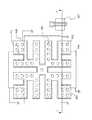
このような半導体装置として、特許文献1に記載の技術がある。図7〜10は、特許文献1に記載の半導体装置におけるスパイラルインダクタを説明する図である。図7は、スパイラルインダクタを有する半導体装置の構成を示す平面図である。図8は、図7のA−A’断面図である。図9は、図7中のポリシリコン205、サイドウォール206、および金属シリサイド208の層を選択的に示した図である。また、図10は、図7中の第一層金属配線211、第二層金属配線214、コンタクトプラグ210、およびビアプラグ213を選択的に示した図である。 As such a semiconductor device, there is a technique described in Patent Document 1. 7 to 10 are diagrams for explaining the spiral inductor in the semiconductor device described in Patent Document 1. FIG. FIG. 7 is a plan view showing a configuration of a semiconductor device having a spiral inductor. FIG. 8 is a cross-sectional view taken along line A-A ′ of FIG. 7. FIG. 9 is a view selectively showing the layers of the
この半導体装置は、導電型がp型のシリコン基板201上に、第一層金属配線211、第二層金属配線214、およびビアプラグ213で形成されたスパイラルインダクタが設けられた構成である。第一層金属配線211は、第一層間絶縁膜209を貫通するコンタクトホール中に埋設されたコンタクトプラグ210を介してMOSFETのソース・ドレイン領域207に接続されている。ソース・ドレイン領域207の導電型はn型である。 This semiconductor device has a configuration in which a spiral inductor formed of a first
また、スパイラルインダクタとシリコン基板201とのカップリングをシールドし、ノイズ発生を抑制するために、スパイラルインダクタとシリコン基板201との間にポリシリコン205が設けられている。ポリシリコン205の上部には、金属シリサイド208が設けられている。ポリシリコン205およびその上部の金属シリサイド208には、インダクタの影響による渦電流の発生を抑えるための切込み215が設けられている。そして、切込み215によってインダクタとシリコン基板201の間のシールド性が低下する分を、切込み領域に整合させてシリコン基板201表面をシリサイド化し、金属シリサイド208を設けることで補うレイアウトとなっている。この構成においては、ポリシリコン205とシリコン基板201の間の絶縁膜として素子分離酸化膜202が用いられている。素子分離酸化膜202の形成には、一般的にSTI(Shallow Trench Isolation)技術が用いられる。 Further, in order to shield the coupling between the spiral inductor and the
また、図11および図12は、特許文献1に記載のスパイラルインダクタの別の例を説明する図である。図11は、別の例について、ポリシリコン205、サイドウォール206、および金属シリサイド208の層を選択的に示した平面図である。また、図12は、図11に示したスパイラルインダクタ領域のA−A’断面図である。この構成においては、ポリシリコン205とシリコン基板201の間の絶縁膜として、p型ウエル203の上部に接して設けられたゲート酸化膜204が用いられている点が、図7〜10に示した装置と異なる。 11 and 12 are diagrams for explaining another example of the spiral inductor described in Patent Document 1. FIG. FIG. 11 is a plan view selectively showing layers of
また、特許文献2には、インダクタ形成領域に、ダミー素子領域を設ける構成のスパイラルインダクタが記載されている。
ところが、本発明者が検討したところ、上記特許文献1に記載の技術について、以下のことが明らかになった。すなわち、図7〜10に示したスパイラルインダクタにおいては、シールドとして使用しているポリシリコン205の直下に、一面にわたって素子分離酸化膜202が形成されていた。このため、インダクタ形成領域において、素子分離酸化膜202が延在している領域の面積が大きく、STI技術を用いて素子分離酸化膜202を形成する際に、酸化膜の研磨工程において、大面積の領域でディッシングが生じることにより、素子分離酸化膜202の膜厚が薄くなり、フィールド段差が発生する懸念があった。なお、このディッシングは、素子分離酸化膜202のデータ密度(当該表面において素子分離酸化膜202が占める面積割合)が局所的に増大することによるものと推察される。 However, as a result of investigation by the present inventor, the following has been clarified regarding the technique described in Patent Document 1. That is, in the spiral inductor shown in FIGS. 7 to 10, the element
フィールド段差が発生すると、後の工程でゲート電極222を形成する際に、PR(フォトレジスト)工程におけるフォーカスのばらつきを発生させ、その結果、ゲート長の寸法のばらつきを増大させる要因となる。スパイラルインダクタの素子占有面積は、一般に、たとえば40000μm2程度と大面積であるため、素子分離酸化膜202の膜厚の不均一さが生じやすく、その後の製造プロセスに影響を与えやすい。When a field step occurs, when forming the
また、図11および図12に示したスパイラルインダクタでは、ポリシリコン205の直下に、シリコン基板表面221の残存領域が大面積にわたって存在していた。このため、ポリシリコン205の直下の領域における素子分離酸化膜202の形成領域の面積が小さく、図7〜図10に示した半導体装置の場合とは逆に、STI技術を用いて素子分離酸化膜202を形成する際に、酸化膜の研磨工程において、酸化膜厚が厚くなる懸念があった。この原因として、インダクタ形成領域の素子分離酸化膜202のデータ密度が局所的に減少することが推察される。 Further, in the spiral inductor shown in FIGS. 11 and 12, the remaining region of the
素子分離酸化膜202の膜厚が局所的に増加すると、フィールド段差が発生するため、この場合にも、ゲート電極222を形成する工程において、ゲート長の寸法のばらつきを増大させる要因となる。また、シリコン基板表面221の面積の割合が大きい場合、STIプロセス完了後、シリコン基板表面221に、除去されるべき酸化膜が残ってしまうなど、製造安定性の低下をもたらす懸念があった。 When the thickness of the element
また、特許文献2におけるダミー素子領域は、CMP工程を制御するために設けられるとされているが、本発明者が検討したところ、後述するように、製造安定性またはシールド性の観点で改善の余地があることが明らかになった。 In addition, the dummy element region in Patent Document 2 is provided to control the CMP process. However, as the inventors have studied, as described later, the dummy element region is improved in terms of manufacturing stability or shielding property. It became clear that there was room.
本発明によれば、
半導体基板と、
前記半導体基板中に埋設された絶縁膜と、
前記半導体基板上に設けられた層間絶縁膜と、
前記層間絶縁膜上に設けられたスパイラルインダクタと、
前記スパイラルインダクタと前記半導体基板との間に、前記半導体基板の表面から絶縁されて前記スパイラルインダクタと前記半導体基板との間を遮蔽するように設けられ、平面視において周縁部から内部に向かう複数の切欠部が設けられた第一のシールド層と、
を有し、
平面視において前記絶縁膜の埋設領域と前記半導体基板の残存領域とにより構成されるダミーパターンが、前記スパイラルインダクタの形成領域において、前記第一のシールド層の直下の領域に選択的に設けられており、
前記ダミーパターンは、前記埋設領域および前記残存領域のうちの一方の中に他方が複数の島状に存在してなることを特徴とする半導体装置が提供される。According to the present invention,
A semiconductor substrate;
An insulating film embedded in the semiconductor substrate;
An interlayer insulating film provided on the semiconductor substrate;
A spiral inductor provided on the interlayer insulating film;
Between the semiconductor substrate and the spiral inductor, the SLbefore being insulated from the semiconductor substrate surfaceis provided so as to shield between the spiral inductor and the semiconductorsubstrate, a plurality toward the inside from the periphery in the plan view A first shield layerprovided with a notch , and
Have,
The dummy pattern composed of the remaining region of the semiconductor substrate and the buried region of the insulating film in theflat surface when viewedfrom, in the formation region of the spiral inductor, selectively providedin a region immediately below the first shield layerand,
Before SL dummy pattern, wherein a the other into one of the said buried region and the remaining region is present in a plurality of islands are provided.
また、本発明によれば、
半導体基板に凹部を設け、該凹部を埋め込むように絶縁膜を形成することにより、前記半導体基板の表面の所定の領域に、平面視において前記絶縁膜の埋設領域と前記半導体基板の残存領域とにより構成されるダミーパターンを形成する工程と、
スパイラルインダクタが形成される領域において、前記半導体基板上に、平面視において周縁部から内部に向かう複数の切欠部が設けられて第一のシールド層となる導電膜を前記半導体基板の表面から絶縁させて形成する工程と、
前記導電膜が設けられた前記半導体基板の上面全面に層間絶縁膜を形成する工程と、
前記層間絶縁膜上に、前記スパイラルインダクタを形成する工程と、
を有し、
ダミーパターンを形成する前記工程において、前記第一のシールド層が形成される領域の直下の領域に選択的に前記ダミーパターンを形成するとともに、前記ダミーパターンを、前記埋設領域および前記残存領域のうちの一方の中に他方が複数の島状に存在するように形成することを特徴とする半導体装置の製造方法が提供される。Moreover, according to the present invention,
By providing a recess in the semiconductor substrate and forming an insulating film so as to embed the recess, a predetermined region on the surface of the semiconductor substrate is formed by the embedded region of the insulating film and the remaining region of the semiconductor substrate in plan view. Forming a dummy pattern to be configured; and
In the region where the spiral inductor is formed, a plurality of notches extending from the periphery to the inside in plan view are provided on the semiconductor substrate to insulate the conductive film serving asthe first shield layer from the surface of the semiconductor substrate. Forming the process,
Forming an interlayer insulating film on the entire upper surface of the semiconductor substrate provided with the conductive film;
Forming the spiral inductor on the interlayer insulating film;
Have
Wherein in the step of forming a dummy pattern, to form a selectively dummy pattern in the region right under the region where thefirst shielding layer is formed,a preKida Me pattern, the buried region and the remaining region There is provided a method for manufacturing a semiconductor device, characterized in that the other is formed in a plurality of islands in one of them.
本発明の半導体装置においては、スパイラルインダクタの形成領域において、埋設領域および残存領域により構成されるダミーパターンが、第一のシールド層の形成領域に選択的に設けられている。そして、スパイラルインダクタの形成領域においては、ダミーパターンは、埋設領域および残存領域のうちの一方の中に他方が複数の島状に存在しているパターンとなっている。スパイラルインダクタの形成領域中のダミーパターンは、埋設領域の中に、残存領域が複数の島状に存在してなる構成であってもよい。このとき、大面積の絶縁膜の埋設領域が基板面内に延在することにより、半導体基板表面において絶縁膜が占める面積割合が局所的に大きくなることを抑制できる。また、スパイラルインダクタの形成領域中のダミーパターンは、残存領域の中に、埋設領域が複数の島状に存在してなる構成であってもよい。このとき、半導体基板の残存領域が大面積にわたって存在することにより、半導体基板表面において絶縁膜が占める面積割合が局所的に小さくなることを抑制することができる。In the semiconductor device of the presentinvention,Te forming regions smell of thescan pie Lalinductor, more composed dummypattern buried region and the remainingarea has selectively provided in the formation region of the first shield layer. In the spiral inductor formation region, the dummy pattern is a pattern in which one of the buried region and the remaining region is present in a plurality of island shapes. The dummy pattern in the formation region of the spiral inductor may have a configuration in which the remaining region exists in a plurality of island shapes in the embedded region. At this time, since the buried region of the large-area insulating film extends in the substrate surface, the area ratio occupied by the insulating film on the surface of the semiconductor substrate can be suppressed from being locally increased. Further, the dummy pattern in the formation region of the spiral inductor may be configured such that the embedded region exists in a plurality of island shapes in the remaining region. At this time, since the remaining region of the semiconductor substrate exists over a large area, it is possible to prevent the area ratio occupied by the insulating film on the surface of the semiconductor substrate from being locally reduced.
このように、本発明においては、ダミーパターンを設けることにより、半導体基板表面において絶縁膜が占める面積割合が他の領域と極端に異なる領域が生じることを抑制することができる。このため、絶縁膜形成時に膜厚が局所的にばらつくことを効果的に抑制可能な構成となっている。よって、スパイラルインダクタが設けられた半導体装置の製造時のフィールド段差の発生を抑制し、製造安定性に優れた構成とすることができる。 Thus, in the present invention, by providing the dummy pattern, it is possible to suppress the generation of a region in which the area ratio occupied by the insulating film on the surface of the semiconductor substrate is extremely different from other regions. For this reason, it is the structure which can suppress effectively that a film thickness varies locally at the time of insulating film formation. Therefore, it is possible to suppress the occurrence of a field step during the manufacture of the semiconductor device provided with the spiral inductor, and to achieve a configuration with excellent manufacturing stability.
また、本発明の製造方法によれば、スパイラルインダクタの形成領域のうち、第一のシールド層が形成される領域の直下の領域に、ダミーパターンが選択的に形成される。このため、絶縁膜の製造時におけるディッシング等を抑制し、絶縁膜の膜厚のばらつきの発生を抑制することができる。よって、スパイラルインダクタを有する半導体装置の製造安定性を向上させることができる。Further, according to the manufacturing method of the present invention, the dummy pattern is selectively formed in a region immediately below the region wherethe first shield layer is formed in the spiral inductor forming region. For this reason, dishing or the like at the time of manufacturing the insulating film can be suppressed, and the occurrence of variations in the film thickness of the insulating film can be suppressed. Therefore, the manufacturing stability of a semiconductor device having a spiral inductor can be improved.
また、本発明においては、スパイラルインダクタの形成領域において、前記半導体基板の表面から絶縁されて設けられた第一のシールド層の直下の領域に選択的にダミーパターンが設けられている。このため、製造安定性を向上させつつ、スパイラルインダクタと半導体基板との間を効果的に遮蔽することができる。よって、スパイラルインダクタと半導体基板とのカップリングを抑制し、これらのカップリングによるノイズの発生を抑制することができる。
In the present invention,Te formation region odor spiralinductor, said selectively dummy pattern in the region directly under the semiconductor substratea first shielding layer provided to be insulated from the surface of the is provided. For this reason, it is possible to effectively shield between the spiral inductor and the semiconductor substrate while improving manufacturing stability. Therefore, the coupling between the spiral inductor and the semiconductor substrate can be suppressed, and the generation of noise due to these couplings can be suppressed.
なお、本発明において、スパイラルインダクタの形成領域においては、第一のシールド層の直下の領域に選択的にダミーパターンが設けられているとは、スパイラルインダクタの形成領域においては、ダミーパターンが実質的に第一のシールド層の直下に設けられ、第一のシールド層の直下の領域における島状の領域の配置密度が高いことをいう。ただし、スパイラルインダクタの形成領域におけるシールド性に大きな影響を与えない程度であれば、第一のシールド層の形成領域以外の領域に島状の領域が設けられていてもよい。また、本発明において、スパイラルインダクタの形成領域以外の領域においては、ダミーパターンが形成されていてもよいし、形成されていなくてもよい。 In the present invention, in the formation area of the spiral inductor, the dummy pattern is selectively provided in the area immediately below the first shield layer. The dummy pattern is substantially formed in the formation area of the spiral inductor. It is provided immediately below the first shield layer, and the arrangement density of the island-like regions in the region immediately below the first shield layer is high. However, an island-like region may be provided in a region other than the region where the first shield layer is formed as long as the shield property in the region where the spiral inductor is formed is not greatly affected. In the present invention, a dummy pattern may or may not be formed in a region other than the spiral inductor formation region.
また、本発明において、スパイラルインダクタは渦巻き状の配線により構成される。配線は単一部材から構成されてもよいし、複数の部材で構成されていてもよい。 In the present invention, the spiral inductor is constituted by a spiral wiring. The wiring may be composed of a single member or may be composed of a plurality of members.
本発明によれば、スパイラルインダクタを有する半導体装置の製造安定性を向上させる技術が実現される。 According to the present invention, a technique for improving the manufacturing stability of a semiconductor device having a spiral inductor is realized.
以下、本発明の実施形態について、図面を用いて説明する。なお、すべての図面において、同様の構成要素には同じ符号を付し、適宜説明を省略する。なお、本明細書において、スパイラルインダクタ形成領域は、平面視において、スパイラルインダクタ120が設けられている全体を指すものとし、渦巻き状の配線と配線の間の領域も含むものとする。また、本明細書において、ポリシリコン形成領域は、平面視において、スパイラルインダクタと半導体基板とをシールドするシールドパターンの形状を有するポリシリコン層が形成されている領域を指すものとする。 Hereinafter, embodiments of the present invention will be described with reference to the drawings. In all the drawings, the same components are denoted by the same reference numerals, and the description thereof is omitted as appropriate. In the present specification, the spiral inductor formation region refers to the entire area where the
(第一の実施形態)
図1〜図4は、本実施形態の半導体装置の構成を示す図である。図1は、半導体装置100の平面図である。図2は、図1のA−A’断面図である。図3は、図1の半導体装置100の、ポリシリコン105、サイドウォール106、および金属シリサイド108を示す平面図である。図4は、図1の半導体装置100の、第一層金属配線111、第二層金属配線114、コンタクトプラグ110、およびビアプラグ113を示す平面図である。(First embodiment)
1 to 4 are diagrams showing the configuration of the semiconductor device of this embodiment. FIG. 1 is a plan view of the semiconductor device 100. 2 is a cross-sectional view taken along line AA ′ of FIG. FIG. 3 is a plan view showing the
図1〜図4に示した半導体装置100は、半導体基板(シリコン基板101)と、シリコン基板101中に埋設された絶縁膜(素子分離酸化膜102)と、シリコン基板101上に設けられた層間絶縁膜(第一層間絶縁膜109、第二層間絶縁膜112)と、第一層間絶縁膜109上に設けられたスパイラルインダクタ120と、スパイラルインダクタ120とシリコン基板101との間に、シリコン基板101の表面から絶縁されて設けられ、基板面内方向に延在し、スパイラルインダクタ120とシリコン基板101との間を遮蔽する第一のシールド層(ポリシリコン105およびポリシリコン105上面の金属シリサイド108)と、を有している。シリコン基板101の表面の所定の領域には、平面視において素子分離酸化膜102の埋設領域とシリコン基板101の残存領域(基板残存領域131)とにより構成されるダミーパターンが設けられている。スパイラルインダクタ120の形成領域においては、ポリシリコン105の直下の領域に選択的にダミーパターンが設けられている。スパイラルインダクタ120の形成領域中のダミーパターンは、埋設領域および基板残存領域131のうちの一方の中に他方が複数の島状に存在してなる構成を有する。
本実施形態では、スパイラルインダクタ120の形成領域中のダミーパターンは、素子分離酸化膜102の埋設領域の中に、基板残存領域131が複数の島状に存在する構成としている。
第一のシールド層は、ポリシリコン105およびその上部の金属シリサイド108からなり、平面視において周縁部から内部に向かう切欠部(切込み115)が設けられている第一の導電膜により構成される。
また、半導体装置100は、切込み115の形成領域に設けられ、切込み115の平面形状に対応する平面形状を有し、シリコン基板101の表面に接して設けられた第二の導電膜(金属シリサイド108)により構成される第二のシールド層を有する。
半導体装置100は、以下の工程により作製される。
(i)シリコン基板101に凹部を設け、該凹部を埋め込むように素子分離酸化膜102を形成することにより、シリコン基板101の表面の所定の領域に、平面視において素子分離酸化膜102の埋設領域と基板残存領域131とにより構成されるダミーパターンを形成する工程、
(ii)スパイラルインダクタ120が形成される領域において、シリコン基板101上に、シールド層となるポリシリコン105をシリコン基板101の表面から絶縁させて形成する工程と、ポリシリコン105が設けられた前記半導体基板の上面全面に第一層間絶縁膜109を形成する工程、
(iii)第一層間絶縁膜109上に、スパイラルインダクタ120を形成する工程。
そして、スパイラルインダクタ120の形成領域においては、ポリシリコン105が形成される領域の直下の領域に選択的にダミーパターンを形成する。また、スパイラルインダクタ120の形成領域中のダミーパターンは、素子分離酸化膜102の埋設領域および基板残存領域131のうちの一方の中に他方が複数の島状に存在するように形成する。
本実施形態では、スパイラルインダクタ120の形成領域中のダミーパターンは、素子分離酸化膜102の埋設領域の中に基板残存領域131が複数の島状に存在してなるダミーパターンを形成する。1 to 4 includes a semiconductor substrate (silicon substrate 101), an insulating film (element isolation oxide film 102) embedded in the
In the present embodiment, the dummy pattern in the formation region of the
The first shield layer is made of
In addition, the semiconductor device 100 is provided in a formation region of the
The semiconductor device 100 is manufactured by the following process.
(I) By providing a recess in the
(Ii) In the region where the
(Iii) A step of forming the
In the formation region of the
In this embodiment, the dummy pattern in the formation region of the
以下、半導体装置100(図1〜図4)について、さらに詳細に説明する。半導体装置100は、導電型がp型のシリコン基板101上に、スパイラルインダクタ120が設けられた構成である。スパイラルインダクタ120は、第一層金属配線111、第一層金属配線111の上部に設けられ渦巻き型の平面形状を有する第二層金属配線114、および第一層金属配線111と第二層金属配線114とを接続するビアプラグ113から構成される。ビアプラグ113は、第二層間絶縁膜112に設けられたビアホール中に充填された導電性のプラグである。シリコン基板101の表面に接して第一層間絶縁膜109が設けられ、第一層間絶縁膜109の上面に接して第二層間絶縁膜112が設けられている。第一層金属配線111は第一層間絶縁膜109の上面に接して設けられており、第二層金属配線114は、第二層間絶縁膜112の上面に接して設けられている。 Hereinafter, the semiconductor device 100 (FIGS. 1 to 4) will be described in more detail. The semiconductor device 100 has a configuration in which a
また、図2に示したように、シリコン基板101上にはMOSFETが設けられている。このMOSFETは、シリコン基板101の表面近傍に設けられたp型ウエル103と、p型ウエル103の表面に接して設けられたゲート酸化膜104と、ゲート酸化膜104の上面に接して設けられたポリシリコン(多結晶シリコン)105とポリシリコン105の上面に接して設けられた金属シリサイド108とからなるゲート電極122と、ゲート電極122の側面外周を被覆するサイドウォール106と、ゲート電極122の形成領域の側方においてp型ウエル103の上部に設けられたソース・ドレイン領域107とを有する。ソース・ドレイン領域107の導電型はn型である。なお、ゲート電極122の上部は、ポリシリコン105がシリサイド化された金属シリサイド108となっている。 In addition, as shown in FIG. 2, a MOSFET is provided on the
スパイラルインダクタ120の第一層金属配線111は、第一層間絶縁膜109を貫通するコンタクトホール中に埋設されたコンタクトプラグ110およびシリコン基板101表面の金属シリサイド108を介して、MOSFETのソース・ドレイン領域107に接続されている。 The first
また、半導体装置100では、スパイラルインダクタ120の形成領域において、素子分離酸化膜102上にポリシリコン105が延在形成されている。ポリシリコン105は、シリコン基板101の上面およびスパイラルインダクタ120から絶縁されており、シリコン基板101とスパイラルインダクタ120との間を遮蔽するシールドパターンとして機能する。スパイラルインダクタ120とシリコン基板101との間にシールドパターンを設けることにより、スパイラルインダクタ120とシリコン基板101とのカップリングをシールドし、ノイズの発生を抑制することができる。 In the semiconductor device 100, the
ポリシリコン105は、第一層間絶縁膜109中に埋設されており、その上面は、ゲート電極122と同様シリサイド化され、金属シリサイド108となっている。ポリシリコン105および金属シリサイド108の側面外周は、サイドウォール106により被覆され、絶縁されている。素子分離酸化膜102は、スパイラルインダクタ120の形成領域のうち、ポリシリコン105およびその側面のサイドウォール106の形成領域に選択的に、これらの底面に接して設けられている。 The
また、平面視において、素子分離酸化膜102中にシリコン基板101が残存する基板残存領域131が複数設けられている。スパイラルインダクタ120の形成領域においては、基板残存領域131はポリシリコン105の形成領域に選択的に設けられている。さらに具体的には、ポリシリコン105の形成領域においては、シリコン基板101に複数の島状領域を残してその周囲に溝部が設けられ、溝部を埋め込むように素子分離酸化膜102が形成されており、この複数の島状領域が基板残存領域131である。半導体装置100では、複数の基板残存領域131の平面形状が矩形で同一形状であり、これらの複数の基板残存領域131が正方格子状に平面配置されたドットパターンとなっている。 In plan view, a plurality of
基板残存領域131の形成箇所においては、シリコン基板101の表面にゲート酸化膜104が設けられている。ポリシリコン105は、底面において素子分離酸化膜102またはゲート酸化膜104に接しており、これらの絶縁膜によってシリコン基板101から絶縁されている。 A
ポリシリコン105の平面形状は、矩形、さらに具体的には正方形であって、四辺のそれぞれについて、周縁から基板面内方向に向かって、渦巻き状の第二層金属配線114を断ち切る方向に切込み115が設けられている。半導体装置100では、切込み115は一辺につき三つ設けられ、三つの切込み115は互いに平行なストライプ状の平面形状を有し、中央の切込み115が一番長く、ポリシリコン105の、より中央側まで切り込まれている。他の二つの切込み115は同じ長さである。また、一つの辺に設けられた切込み115と他の辺に設けられた切込み115とは連通していない。 The planar shape of the
また、切込み115の形成領域に対応する領域において、シリコン基板101の表面がシリサイド化され、金属シリサイド108となっている。平面視において、金属シリサイド108は、ポリシリコン105の各辺の側方から切込み115内にわたって延在しており、凹状に設けられた切込み115に係合する凸状の平面形状を有する。シリコン基板101の表面に設けられた金属シリサイド108も、シールドパターンとして機能する。シリコン基板101上に、切込み115の平面形状に対応する平面形状を有する金属シリサイド108のシールドパターンを設けることにより、切込み115を設けることに起因するスパイラルインダクタ120とシリコン基板101の間のシールド性の低下を補うことが可能なレイアウトが実現される。これらのシールドパターンは、サイドウォール106および素子分離酸化膜102により互いに絶縁され、いずれも、接地端子(不図示)に接続される。 Further, in the region corresponding to the formation region of the
次に、図1〜図4に示した半導体装置100の製造方法を説明する。
まず、シリコン基板101の表面の所定の領域に、通常のSTI形成プロセスを用いて素子分離酸化膜102を選択的に形成する。素子分離酸化膜102の材料は、たとえばSiO2膜とする。本実施形態では、素子分離酸化膜102を、スパイラルインダクタ120形成領域のうち、ポリシリコン105の形成領域に選択的に設け、切込み115の形成領域には設けない。ポリシリコン105の形成領域においては、素子分離酸化膜102中に基板残存領域131を設ける。具体的には、シリコン基板101に複数の島状領域を基板残存領域131として残してその周囲に溝部を設け、溝部を埋め込むようにSiO2膜を形成することにより、基板残存領域131の側面外周が素子分離酸化膜102で覆われた構成を得る。Next, a method for manufacturing the semiconductor device 100 shown in FIGS. 1 to 4 will be described.
First, an element
次に、シリコン基板101の表面近傍にp型ウエル103を形成する。そして、シリコン基板101の表面を酸化し、ゲート酸化膜104となるSiO2膜を成長させる。つづいて、ゲート酸化膜104が設けられたシリコン基板101の上面全面に、ポリシリコン膜を成長させる。フォトリソグラフィー技術を用いてp型ウエル103の上部に設けられるゲート電極122の形成領域およびシールドパターンの形成領域以外の領域を開口部とするマスクパターンを形成し、このマスクを用いてポリシリコン105を選択的に除去する。これにより、ゲート電極122を構成するポリシリコン105およびシールドパターンとして機能するポリシリコン105を同一水準に同時に得ることができる。Next, a p-
次に、サイドウォール106となる絶縁膜として、たとえばSiO2膜を成長させる。そして、このSiO2膜をエッチバックして、ポリシリコン105の側面にサイドウォール106を形成する。その後、n型のソース・ドレイン領域107をイオン注入法により形成し、RTA(ラピッドサーマルアニーリング)法により熱処理を行い、ソース・ドレイン領域107の不純物を活性化させる。Next, for example, a SiO2 film is grown as an insulating film to be the
その後、金属シリサイド108が設けられる領域のシリコン基板101の表面およびポリシリコン105の表面を露出させる。そして、たとえば金属としてコバルト(Co)膜をシリコン基板101の上面全面に形成する。これを熱処理して、MOSFETのゲート電極122をなすポリシリコン105、ソース・ドレイン領域107、スパイラルインダクタ120形成予定領域直下のポリシリコン105、および切込み115形成領域のシリコン基板101の表面に、それぞれ金属シリサイド108の層を形成する。 Thereafter, the surface of the
その後、シリコン基板101の上面全面に第一層間絶縁膜109を成長させ、フォトリソグラフィーおよびエッチングを用いてコンタクトプラグ110を設ける領域にコンタクトホールを形成する。コンタクトホールにタングステン(W)等の金属膜を埋め込んだ後、アルミニウム(Al)等の金属膜を成長させる。フォトリソグラフィーおよびエッチングにより、第一層間絶縁膜109の上部において第一層金属配線111の形成領域以外に設けられた金属膜を除去し、コンタクトプラグ110および第一層金属配線111を得る。 Thereafter, a first
そして、第一層間絶縁膜109の上面全面に第二層間絶縁膜112を形成し、フォトリソグラフィーおよびエッチングを用いてビアホールを形成する。ビアホールにビアプラグ113となるタングステン等の金属膜を埋め込んだ後、アルミニウム等の金属膜を成長させる。フォトリソグラフィーおよびエッチングにより、第二層間絶縁膜112の上部において第二層金属配線114の形成領域以外に設けられた金属膜を除去し、ビアプラグ113および第二層金属配線114を得る。以上の工程により、半導体装置100が得られる。 Then, a second
なお、第一層間絶縁膜109および第二層間絶縁膜112は、たとえばSiO2膜とする。また、これらの層間絶縁膜を、低誘電率膜としてもよい。なお、本明細書において、低誘電率膜とは、たとえば比誘電率kが3.5以下の膜を指す。このような膜として、たとえばSiOC膜、水素化ポリシロキサン膜、メチルポリシロキサン膜、水素化メチルポリシロキサン膜、またはこれらの膜をポーラス化したもの等が挙げられる。また、低誘電率膜として、有機ポリマーを用いてもよい。The first
次に、図1〜図4に示した半導体装置100の効果を説明する。
半導体装置100においては、スパイラルインダクタ120の形成領域においては、ポリシリコン105の直下の領域に選択的に、素子分離酸化膜102に欠損部が設けられて複数の基板残存領域131となっており、基板残存領域131が正方格子状に平面配置されて、ドット状のダミーパターンを構成している。基板残存領域131は、素子分離酸化膜102の作製(研磨工程)時の、膜厚変動抑制パターンとして機能する。このため、一般に大面積となるスパイラルインダクタ120の形成領域についても、素子分離酸化膜102が大面積の平板状に延在している構成に比べて、素子分離酸化膜102となる酸化膜の研磨時にディッシングが生じることを抑制できる。よって、STIプロセスによる素子分離酸化膜102の形成過程におけるフィールド段差の発生を抑制することができる。したがって、素子分離酸化膜102の形成工程以降のゲート電極122の形成工程において、ゲート長の寸法ばらつきの発生を抑制可能な構成となっている。Next, the effect of the semiconductor device 100 shown in FIGS. 1 to 4 will be described.
In the semiconductor device 100, in the formation region of the
この原因は、基板残存領域131を設けることにより、素子分離酸化膜102のデータ密度(当該表面における素子分離酸化膜102が占める面積割合)が局所的に過度に高くなることが抑制され、スパイラルインダクタ120の形成領域外の領域における素子分離酸化膜102のデータ密度に近づけることができ、シリコン基板101上の素子分離酸化膜102のデータ密度を均一にすることができるためであると推察される。 The reason for this is that by providing the
また、ポリシリコン105には、渦巻き状の第二層金属配線114を断ち切る方向に切込み115が設けられているため、切込み115を有しない一つの平板状のシールドパターンを設けた場合に比べて、渦電流の発生を抑制し、クオリティーファクター(Q値)の低下を防止することができる。 In addition, since the
さらに、半導体装置100においては、シリコン基板101の表面に設けられた金属シリサイド108からなるシールドパターンと、ポリシリコン105と金属シリサイド108の積層膜からなるシールドパターンの、二つのシールドパターンが基板面内に互いに係合して配置されている。このため、ポリシリコン105に切込み115を設けた場合においても、切込み115形成箇所におけるシールド性の低下をさらに確実に抑制し、第二層金属配線114とシリコン基板101とのカップリングによる基板ノイズの発生をより一層効果的に防止することができる。なお、ポリシリコン105の平面形状および切込み115の数は、図示した態様に限られるものではなく、ポリシリコン105およびシリコン基板101表面の金属シリサイド108によって渦電流の抑制とシールド性が確保される構成となっていればよい。 Furthermore, in the semiconductor device 100, two shield patterns, that is, a shield pattern made of a
以上のように、半導体装置100では、スパイラルインダクタ120とシリコン基板101の間のシールド性を損なうことなく、クオリティーファクターの低下を抑制するとともに、製造安定性に優れた構成が実現されている。 As described above, in the semiconductor device 100, a configuration excellent in manufacturing stability is realized while suppressing a decrease in quality factor without impairing the shielding performance between the
なお、背景技術の項で前述した特許文献2に記載の技術を特許文献1に記載の技術(たとえば図7)を組み合わせた場合には、特許文献2におけるダミーパターンが、スパイラルインダクタの形成領域およびその近傍の全面にわたって配置されるため、ポリシリコン205の直下だけでなく、ポリシリコン205の切込み215に整合して形成された、シリコン基板201表面の金属シリサイド208の直下の領域にもダミーパターンが配置されることになる。 When the technique described in Patent Document 2 described above in the background art section is combined with the technique described in Patent Document 1 (for example, FIG. 7), the dummy pattern in Patent Document 2 is used to form a spiral inductor formation region and Since it is arranged over the entire surface in the vicinity, a dummy pattern is formed not only directly under the
ところが、本発明者が検討した結果、たとえば図7の構成においてシリコン基板201表面の金属シリサイド208の直下にダミーパターンを設けようとすると、ダミーパターンの形成領域には素子分離酸化膜202が設けられることになるため、シリコン基板201の表面の露出面積が減少し、金属シリサイド208が形成される領域の面積が減少する。これにより、スパイラルインダクタとシリコン基板201との間のシールド性が低下してしまい、カップリングによるノイズの発生が顕著になる懸念があることが明らかになった。 However, as a result of the study by the present inventors, for example, in the configuration of FIG. 7, when an attempt is made to provide a dummy pattern immediately below the
また、特許文献2には、ダミーパターンを、スパイラル配線の形成領域以外の領域にのみ設ける構成も記載されている。ところが、この構成の場合も、上述した金属シリサイド208の形成領域の面積の減少により、ノイズの抑制が不充分となる懸念があった。また、スパイラル配線の形成領域の直下の全面に素子分離酸化膜202が設けられるため、素子分離酸化膜202にディッシングが生じやすく、フィールド段差の抑制が不充分となる懸念があった。 Patent Document 2 also describes a configuration in which a dummy pattern is provided only in a region other than the spiral wiring formation region. However, even in this configuration, there is a concern that the suppression of noise becomes insufficient due to the reduction in the area of the formation region of the
これに対し、本実施形態の構成では、ドット状の基板残存領域131が、シリコン基板101上面から絶縁されたポリシリコン形成領域に選択的に設けられており、シリコン基板101に接して設けられた金属シリサイド108の下部にはドット状の基板残存領域131が設けられていない。このため、シリコン基板101およびポリシリコン105を同時にシリサイド化する簡便なプロセスによって、切込み115の形状に対応する領域全体に金属シリサイド108を設け、シールドパターンとして機能させることができる。よって、素子分離酸化膜102形成時のディッシングの抑制効果を充分に確保しつつ、シールド性の低下を充分に抑制することが可能な構成となっている。 On the other hand, in the configuration of the present embodiment, the dot-like
(第二の実施形態)
第一の実施形態においては、素子分離酸化膜102中に島状の基板残存領域131が残存しているダミーパターンの場合を例示したが、ダミーパターンは、素子分離酸化膜102と基板残存領域131とが反転したパターンであってもよい。本実施形態では、素子分離酸化膜102と基板残存領域131とが反転したパターンをダミーパターンを有する構成の半導体装置について、第一の実施形態と異なる点を中心に説明する。(Second embodiment)
In the first embodiment, the dummy pattern in which the island-like
図5および図6は、本実施形態に係る半導体装置の構成を示す図である。図5は、半導体装置の、ポリシリコン105、サイドウォール106、および金属シリサイド108を示す平面図である。図6は、半導体装置の断面図であり、図5のA−A’断面を示す図である。 5 and 6 are diagrams illustrating the configuration of the semiconductor device according to the present embodiment. FIG. 5 is a plan view showing the
図5および図6に示した半導体装置の基本構成は第一の実施形態の半導体装置と同様であるが、シールドパターンにおけるポリシリコン105および金属シリサイド108の平面形状が、図11を参照して前述した形状となっている点が異なる。 The basic configuration of the semiconductor device shown in FIGS. 5 and 6 is the same as that of the semiconductor device of the first embodiment, but the planar shapes of the
また、図5および図6に示したように、本実施形態では、スパイラルインダクタ120の形成領域中のダミーパターンは、基板残存領域131の中に、素子分離酸化膜102の埋設領域が複数の島状に存在してなる点も異なる。島状に設けられた素子分離酸化膜102は、素子分離酸化膜102作製時の膜厚変動を抑制するダミーパターンとして機能し、その平面形状および平面配置は、第一の実施形態における基板残存領域131と同様、正方格子状に配置されたドットパターンとなっている。この半導体装置は、スパイラルインダクタ120の形成領域においては、基板残存領域131の中に素子分離酸化膜102の埋設領域が複数の島状に存在してなるダミーパターンを形成することにより製造される。 Further, as shown in FIGS. 5 and 6, in this embodiment, the dummy pattern in the formation region of the
本実施形態の半導体装置(図5〜図6)においては、ポリシリコン105の形成領域に、素子分離酸化膜102のドットパターンが設けられている。このため、図11および図12を参照して前述した構成に比べ、ポリシリコン105直下にシリコン基板表面121が大面積にわたって残存しない構成とすることができる。このため、素子分離酸化膜102の占める面積の割合を高めることができるので、STIプロセスによる素子分離酸化膜102の形成の過程において、フィールド段差が発生することを抑制可能な構成とすることができる。また、STIプロセス完了後、シリコン基板101の表面に、除去されるべき酸化膜が残存しないようにすることができる。よって、本実施形態においても、第一の実施形態と同様に、スパイラルインダクタ120とシリコン基板101との間のシールド性を充分に確保しつつ、フィールド段差に起因するゲート長のばらつきを抑制し、製造安定性に優れた構成とすることができる。 In the semiconductor device of this embodiment (FIGS. 5 to 6), the dot pattern of the element
以上、図面を参照して本発明の実施形態について述べたが、これらは本発明の例示であり、上記以外の様々な構成を採用することもできる。 As mentioned above, although embodiment of this invention was described with reference to drawings, these are the illustrations of this invention, Various structures other than the above are also employable.
たとえば、以上の実施形態においては、ポリシリコン105の直下に並べて配置した基板残存領域131または素子分離酸化膜102の平面形状が正方形のドット形状である場合を例に説明したが、ダミーパターンはドットパターンである必要はなく、平面視においてストライプ状にシリコン基板101が残存しているスリットパターンや任意の多角形等の平面形状であってもよい。 For example, in the above embodiment, the case where the planar shape of the
また、以上においては、複数のドット状の基板残存領域131または素子分離酸化膜102が正方格子状に平面配置されている場合を例に説明したが、ドットパターンの平面配置は正方格子状には限られず、たとえば、千鳥格子等の斜格子状など、他の格子状としてもよい。また、ドットパターンをポリシリコン105の直下の領域にランダムに配置してもよい。 In the above description, the case where a plurality of dot-like
また、以上においては、シールドパターンとなるポリシリコン105および金属シリサイド108を、スパイラルインダクタ120の形成領域全体およびその近傍に形成したが、このシールドパターンは導電膜により構成されていればよい。また、シールドパターンは、少なくとも第二層金属配線114および第一層金属配線111とシリコン基板101との間の領域に形成されていればよい。これらの配線が設けられていない領域も含めて、スパイラルインダクタ120の形成領域全体に金属シリサイド108のシールドパターンを設けることにより、シールド効果をより一層確実に発揮させることができる。 In the above description, the
100 半導体装置
101 シリコン基板
102 素子分離酸化膜
103 p型ウエル
104 ゲート酸化膜
105 ポリシリコン
106 サイドウォール
107 ソース・ドレイン領域
108 金属シリサイド
109 第一層間絶縁膜
110 コンタクトプラグ
111 第一層金属配線
112 第二層間絶縁膜
113 ビアプラグ
114 第二層金属配線
115 切込み
120 スパイラルインダクタ
121 シリコン基板表面
122 ゲート電極
131 基板残存領域
DESCRIPTION OF SYMBOLS 100
Claims (7)
Translated fromJapanese前記半導体基板中に埋設された絶縁膜と、
前記半導体基板上に設けられた層間絶縁膜と、
前記層間絶縁膜上に設けられたスパイラルインダクタと、
前記スパイラルインダクタと前記半導体基板との間に、前記半導体基板の表面から絶縁されて前記スパイラルインダクタと前記半導体基板との間を遮蔽するように設けられ、平面視において周縁部から内部に向かう複数の切欠部が設けられた第一のシールド層と、
を有し、
平面視において前記絶縁膜の埋設領域と前記半導体基板の残存領域とにより構成されるダミーパターンが、前記スパイラルインダクタの形成領域において、前記第一のシールド層の直下の領域に選択的に設けられており、
前記ダミーパターンは、前記埋設領域および前記残存領域のうちの一方の中に他方が複数の島状に存在してなることを特徴とする半導体装置。A semiconductor substrate;
An insulating film embedded in the semiconductor substrate;
An interlayer insulating film provided on the semiconductor substrate;
A spiral inductor provided on the interlayer insulating film;
Between the semiconductor substrate and the spiral inductor, the SLbefore being insulated from the semiconductor substrate surfaceis provided so as to shield between the spiral inductor and the semiconductorsubstrate, a plurality toward the inside from the periphery in the plan view A first shield layerprovided with a notch , and
Have,
The dummy pattern composed of the remaining region of the semiconductor substrate and the buried region of the insulating film in theflat surface when viewedfrom, in the formation region of the spiral inductor, selectively providedin a region immediately below the first shield layerand,
Before SL dummy pattern, wherein a the other into one of the said buried region and the remaining region is present in a plurality of islands.
前記複数の切欠部の形成領域に設けられ、前記切欠部の平面形状に対応する平面形状を有し、前記半導体基板の表面に接して設けられた第二のシールド層をさらに有し、
前記ダミーパターンが、前記第二のシールド層の下に設けられていないことを特徴とする半導体装置。The semiconductor device accordingto claim1,
Provided forming regionbefore Symbolplurality of cutout portions has a planar shape corresponding to the planar shape of the cut portion,furtherhave asecond shieldlayer in contact with the surface of the semiconductorsubstrate,
The semiconductor device, wherein the dummy pattern is not provided under the second shield layer .
前記ダミーパターンの前記埋設領域は、前記スパイラルインダクタを形成する領域内において分離されることなく形成され、前記ダミーパターンの前記残存領域は、前記埋設領域の中に複数の島状に存在してなることを特徴とする半導体装置。The semiconductor device according to claim2 ,
It said buried regionbefore Symbol dummy pattern,the formed without being separated in the region for forming the spiral inductor, the remaining areaof the dummy patternis present in a plurality of islandsin the embedded region A semiconductor device comprising:
前記ダミーパターンの前記残存領域は、前記スパイラルインダクタを形成する領域内において分離されることなく形成され、前記ダミーパターンの前記埋設領域は、前記残存領域の中に複数の島状に存在してなることを特徴とする半導体装置。The semiconductor device according to claim2,
The remaining regionbefore Symbol dummy pattern,the formed without being separated in the region for forming the spiral inductor, the buried regionof the dummy patternis present in a plurality of islandsin the remaining region A semiconductor device comprising:
スパイラルインダクタが形成される領域において、前記半導体基板上に、平面視において周縁部から内部に向かう複数の切欠部が設けられて第一のシールド層となる導電膜を前記半導体基板の表面から絶縁させて形成する工程と、
前記導電膜が設けられた前記半導体基板の上面全面に層間絶縁膜を形成する工程と、
前記層間絶縁膜上に、前記スパイラルインダクタを形成する工程と、
を有し、
ダミーパターンを形成する前記工程において、前記第一のシールド層が形成される領域の直下の領域に選択的に前記ダミーパターンを形成するとともに、前記ダミーパターンを、前記埋設領域および前記残存領域のうちの一方の中に他方が複数の島状に存在するように形成することを特徴とする半導体装置の製造方法。By providing a recess in the semiconductor substrate and forming an insulating film so as to embed the recess, a predetermined region on the surface of the semiconductor substrate is formed by the embedded region of the insulating film and the remaining region of the semiconductor substrate in plan view. Forming a dummy pattern to be configured; and
In the region where the spiral inductor is formed, a plurality of notches extending from the periphery to the inside in plan view are provided on the semiconductor substrate to insulate the conductive film serving asthe first shield layer from the surface of the semiconductor substrate. Forming the process,
Forming an interlayer insulating film on the entire upper surface of the semiconductor substrate provided with the conductive film;
Forming the spiral inductor on the interlayer insulating film;
Have
Wherein in the step of forming a dummy pattern, to form a selectively dummy pattern in the region right under the region where thefirst shielding layer is formed,a preKida Me pattern, the buried region and the remaining region A method for manufacturing a semiconductor device, characterized in that one of the two is formed in a plurality of islands.
ダミーパターンを形成する前記工程において、ダミーパターンの前記埋設領域を、前記スパイラルインダクタを形成する領域内において分離されることなく形成するとともに、前記残存領域を、前記埋設領域の中に複数の島状に形成することを特徴とする半導体装置の製造方法。In the manufacturing method of the semiconductor device according to claim 5,
Wherein in the step of forming adummypattern, the buried region of the dummy pattern, wherein as to form without being separated in the region for forming the spiral inductor, the remaining area,multiple in said buried region the method of manufacturing a semiconductor device, characterized by thatform anisland shape.
ダミーパターンを形成する前記工程において、ダミーパターンの前記残存領域を、前記スパイラルインダクタを形成する領域内において分離されることなく形成するとともに、前記埋設領域を、前記残存領域の中に複数の島状に形成することを特徴とする半導体装置の製造方法。In the manufacturing method of the semiconductor device according to claim 5,
Wherein in the step of forming adummypattern, the remaining area of the dummy pattern, so as to form without being separated in the region for forming the spiral inductor, said buried region,multiple in said remaining region the method of manufacturing a semiconductor device, characterized by thatform anisland shape.
Priority Applications (4)
| Application Number | Priority Date | Filing Date | Title |
|---|---|---|---|
| JP2004322838AJP4795667B2 (en) | 2004-11-05 | 2004-11-05 | Semiconductor device and manufacturing method thereof |
| EP05023414AEP1655746A3 (en) | 2004-11-05 | 2005-10-26 | Integrated spiral inductor including a shielding layer |
| KR1020050103058AKR100652231B1 (en) | 2004-11-05 | 2005-10-31 | Semiconductor device and method for manufacturing same |
| US11/267,248US7310040B2 (en) | 2004-11-05 | 2005-11-07 | Semiconductor device and method for manufacturing same |
Applications Claiming Priority (1)
| Application Number | Priority Date | Filing Date | Title |
|---|---|---|---|
| JP2004322838AJP4795667B2 (en) | 2004-11-05 | 2004-11-05 | Semiconductor device and manufacturing method thereof |
Publications (2)
| Publication Number | Publication Date |
|---|---|
| JP2006135107A JP2006135107A (en) | 2006-05-25 |
| JP4795667B2true JP4795667B2 (en) | 2011-10-19 |
Family
ID=35871057
Family Applications (1)
| Application Number | Title | Priority Date | Filing Date |
|---|---|---|---|
| JP2004322838AExpired - Fee RelatedJP4795667B2 (en) | 2004-11-05 | 2004-11-05 | Semiconductor device and manufacturing method thereof |
Country Status (4)
| Country | Link |
|---|---|
| US (1) | US7310040B2 (en) |
| EP (1) | EP1655746A3 (en) |
| JP (1) | JP4795667B2 (en) |
| KR (1) | KR100652231B1 (en) |
Families Citing this family (9)
| Publication number | Priority date | Publication date | Assignee | Title |
|---|---|---|---|---|
| WO2007080531A1 (en)* | 2006-01-09 | 2007-07-19 | Nxp B.V. | Integrated circuit inductor with small floating metal structures |
| DE102006057332B4 (en)* | 2006-12-05 | 2018-01-25 | Infineon Technologies Ag | Assembly comprising a substrate and a chip mounted on the substrate |
| US7750408B2 (en) | 2007-03-29 | 2010-07-06 | International Business Machines Corporation | Integrated circuit structure incorporating an inductor, a conductive sheet and a protection circuit |
| US7652355B2 (en) | 2007-08-01 | 2010-01-26 | Chartered Semiconductor Manufacturing, Ltd. | Integrated circuit shield structure |
| TWI399139B (en)* | 2007-09-19 | 2013-06-11 | Ind Tech Res Inst | Meander inductor and printed circuit board with a meander inductor |
| US7598588B2 (en) | 2007-10-26 | 2009-10-06 | Hvvi Semiconductors, Inc | Semiconductor structure and method of manufacture |
| US20100180430A1 (en)* | 2009-01-22 | 2010-07-22 | Mvm Technologies, Inc. | Spiral Inductors |
| US8697517B2 (en)* | 2010-03-16 | 2014-04-15 | Taiwan Semiconductor Manufacturing Company, Ltd. | Reduced substrate coupling for inductors in semiconductor devices |
| KR20210085421A (en)* | 2019-12-30 | 2021-07-08 | 에스케이하이닉스 주식회사 | Semiconductor device |
Family Cites Families (9)
| Publication number | Priority date | Publication date | Assignee | Title |
|---|---|---|---|---|
| JPH10321802A (en)* | 1997-05-22 | 1998-12-04 | Toshiba Corp | Inductor element |
| JP3488164B2 (en)* | 2000-02-14 | 2004-01-19 | Necエレクトロニクス株式会社 | Semiconductor device |
| JP2002009299A (en)* | 2000-04-17 | 2002-01-11 | Mitsubishi Electric Corp | Method for manufacturing semiconductor device |
| JP4776752B2 (en)* | 2000-04-19 | 2011-09-21 | ルネサスエレクトロニクス株式会社 | Semiconductor device |
| JP4969715B2 (en)* | 2000-06-06 | 2012-07-04 | ルネサスエレクトロニクス株式会社 | Semiconductor device |
| JP2002110908A (en)* | 2000-09-28 | 2002-04-12 | Toshiba Corp | Spiral inductor and method of manufacturing semiconductor integrated circuit device having the same |
| US6777774B2 (en)* | 2002-04-17 | 2004-08-17 | Chartered Semiconductor Manufacturing Limited | Low noise inductor using electrically floating high resistive and grounded low resistive patterned shield |
| JP4408023B2 (en)* | 2002-05-10 | 2010-02-03 | 三菱電機株式会社 | Semiconductor device |
| JP2004265989A (en)* | 2003-02-28 | 2004-09-24 | Matsushita Electric Ind Co Ltd | Method for manufacturing semiconductor device |
- 2004
- 2004-11-05JPJP2004322838Apatent/JP4795667B2/ennot_activeExpired - Fee Related
- 2005
- 2005-10-26EPEP05023414Apatent/EP1655746A3/ennot_activeWithdrawn
- 2005-10-31KRKR1020050103058Apatent/KR100652231B1/ennot_activeExpired - Fee Related
- 2005-11-07USUS11/267,248patent/US7310040B2/ennot_activeExpired - Fee Related
Also Published As
| Publication number | Publication date |
|---|---|
| KR20060052362A (en) | 2006-05-19 |
| JP2006135107A (en) | 2006-05-25 |
| US20060097836A1 (en) | 2006-05-11 |
| EP1655746A3 (en) | 2009-07-22 |
| KR100652231B1 (en) | 2006-12-01 |
| EP1655746A2 (en) | 2006-05-10 |
| US7310040B2 (en) | 2007-12-18 |
Similar Documents
| Publication | Publication Date | Title |
|---|---|---|
| US6649490B1 (en) | Methods for forming integrated circuit devices through selective etching of an insulation layer to increase the self-aligned contact area adjacent a semiconductor region and integrated circuit devices formed thereby | |
| US6927461B2 (en) | Semiconductor device having shared contact and fabrication method thereof | |
| US8975173B2 (en) | Semiconductor device with buried gate and method for fabricating the same | |
| US7872329B2 (en) | Semiconductor device and method of manufacturing the same | |
| KR101699443B1 (en) | Method for manufacturing semiconductor device having vertical channel transistor | |
| JP5073157B2 (en) | Semiconductor device | |
| JP2002110908A (en) | Spiral inductor and method of manufacturing semiconductor integrated circuit device having the same | |
| KR102693515B1 (en) | Integrated circuit device | |
| KR20010014640A (en) | Semiconductor device and method for manufacturing the same | |
| JP2006344943A (en) | Mos field effect transistor having trench isolation region and method of fabricating the same | |
| JP2006339621A (en) | Manufacturing method of semiconductor device | |
| JP2004023098A (en) | Method for manufacturing semiconductor device | |
| JP2006019661A (en) | Semiconductor device and manufacturing method thereof | |
| KR100688552B1 (en) | A MOS field effect transistor having a thick edge gate insulating film pattern and a manufacturing method thereof | |
| JP4795667B2 (en) | Semiconductor device and manufacturing method thereof | |
| US8530975B2 (en) | Semiconductor device with gate edge protrusion | |
| US7375016B2 (en) | Method for fabricating semiconductor device | |
| JP2008034793A (en) | Semiconductor device and manufacturing method thereof | |
| JP2009123882A (en) | Semiconductor device and manufacturing method thereof | |
| JP2009252825A (en) | Semiconductor device and manufacturing method therefor | |
| US7645653B2 (en) | Method for manufacturing a semiconductor device having a polymetal gate electrode structure | |
| KR101001152B1 (en) | Semiconductor device manufacturing method | |
| KR20080084258A (en) | Method of forming a semiconductor device | |
| KR100594293B1 (en) | Semiconductor device having recess channel transistor and manufacturing method thereof | |
| JPH11145287A (en) | Semiconductor device and method of manufacturing semiconductor device |
Legal Events
| Date | Code | Title | Description |
|---|---|---|---|
| A621 | Written request for application examination | Free format text:JAPANESE INTERMEDIATE CODE: A621 Effective date:20071015 | |
| A977 | Report on retrieval | Free format text:JAPANESE INTERMEDIATE CODE: A971007 Effective date:20100723 | |
| A131 | Notification of reasons for refusal | Free format text:JAPANESE INTERMEDIATE CODE: A131 Effective date:20100727 | |
| A521 | Request for written amendment filed | Free format text:JAPANESE INTERMEDIATE CODE: A523 Effective date:20100927 | |
| TRDD | Decision of grant or rejection written | ||
| A01 | Written decision to grant a patent or to grant a registration (utility model) | Free format text:JAPANESE INTERMEDIATE CODE: A01 Effective date:20110726 | |
| A01 | Written decision to grant a patent or to grant a registration (utility model) | Free format text:JAPANESE INTERMEDIATE CODE: A01 | |
| A61 | First payment of annual fees (during grant procedure) | Free format text:JAPANESE INTERMEDIATE CODE: A61 Effective date:20110728 | |
| R150 | Certificate of patent or registration of utility model | Ref document number:4795667 Country of ref document:JP Free format text:JAPANESE INTERMEDIATE CODE: R150 Free format text:JAPANESE INTERMEDIATE CODE: R150 | |
| FPAY | Renewal fee payment (event date is renewal date of database) | Free format text:PAYMENT UNTIL: 20140805 Year of fee payment:3 | |
| S531 | Written request for registration of change of domicile | Free format text:JAPANESE INTERMEDIATE CODE: R313531 | |
| R350 | Written notification of registration of transfer | Free format text:JAPANESE INTERMEDIATE CODE: R350 | |
| LAPS | Cancellation because of no payment of annual fees |