JP4792571B2 - PVD coating equipment - Google Patents
PVD coating equipmentDownload PDFInfo
- Publication number
- JP4792571B2 JP4792571B2JP54347198AJP54347198AJP4792571B2JP 4792571 B2JP4792571 B2JP 4792571B2JP 54347198 AJP54347198 AJP 54347198AJP 54347198 AJP54347198 AJP 54347198AJP 4792571 B2JP4792571 B2JP 4792571B2
- Authority
- JP
- Japan
- Prior art keywords
- substrate
- anode
- potential
- voltage
- cathode
- Prior art date
- Legal status (The legal status is an assumption and is not a legal conclusion. Google has not performed a legal analysis and makes no representation as to the accuracy of the status listed.)
- Expired - Lifetime
Links
- 238000000576coating methodMethods0.000titleclaimsdescription60
- 239000011248coating agentSubstances0.000titleclaimsdescription49
- 239000000758substrateSubstances0.000claimsdescription108
- 238000005240physical vapour depositionMethods0.000claimsdescription26
- 238000000034methodMethods0.000claimsdescription14
- 238000004544sputter depositionMethods0.000claimsdescription7
- 210000002381plasmaAnatomy0.000description31
- 239000007789gasSubstances0.000description27
- 150000002500ionsChemical class0.000description17
- 239000013077target materialSubstances0.000description15
- 238000000151depositionMethods0.000description8
- 229910052751metalInorganic materials0.000description8
- 239000002184metalSubstances0.000description8
- 239000010406cathode materialSubstances0.000description7
- 230000008021depositionEffects0.000description7
- 239000000463materialSubstances0.000description7
- 238000010586diagramMethods0.000description6
- IJGRMHOSHXDMSA-UHFFFAOYSA-NAtomic nitrogenChemical compoundN#NIJGRMHOSHXDMSA-UHFFFAOYSA-N0.000description4
- 239000002245particleSubstances0.000description4
- RTAQQCXQSZGOHL-UHFFFAOYSA-NTitaniumChemical compound[Ti]RTAQQCXQSZGOHL-UHFFFAOYSA-N0.000description3
- 229910052782aluminiumInorganic materials0.000description3
- XAGFODPZIPBFFR-UHFFFAOYSA-NaluminiumChemical compound[Al]XAGFODPZIPBFFR-UHFFFAOYSA-N0.000description3
- 239000002800charge carrierSubstances0.000description3
- 238000009826distributionMethods0.000description3
- 230000000694effectsEffects0.000description3
- 238000010891electric arcMethods0.000description3
- 238000012986modificationMethods0.000description3
- 230000004048modificationEffects0.000description3
- 238000005498polishingMethods0.000description3
- 239000002994raw materialSubstances0.000description3
- 239000010936titaniumSubstances0.000description3
- 229910052719titaniumInorganic materials0.000description3
- XKRFYHLGVUSROY-UHFFFAOYSA-NArgonChemical compound[Ar]XKRFYHLGVUSROY-UHFFFAOYSA-N0.000description2
- -1CH 4Chemical compound0.000description2
- PXHVJJICTQNCMI-UHFFFAOYSA-NNickelChemical compound[Ni]PXHVJJICTQNCMI-UHFFFAOYSA-N0.000description2
- 229910010037TiAlNInorganic materials0.000description2
- 229910052799carbonInorganic materials0.000description2
- 238000006243chemical reactionMethods0.000description2
- 230000005684electric fieldEffects0.000description2
- 230000005611electricityEffects0.000description2
- 238000001704evaporationMethods0.000description2
- 238000000227grindingMethods0.000description2
- 239000000155meltSubstances0.000description2
- 229910052757nitrogenInorganic materials0.000description2
- BASFCYQUMIYNBI-UHFFFAOYSA-NplatinumChemical compound[Pt]BASFCYQUMIYNBI-UHFFFAOYSA-N0.000description2
- 239000007787solidSubstances0.000description2
- OKTJSMMVPCPJKN-UHFFFAOYSA-NCarbonChemical compound[C]OKTJSMMVPCPJKN-UHFFFAOYSA-N0.000description1
- VYZAMTAEIAYCRO-UHFFFAOYSA-NChromiumChemical compound[Cr]VYZAMTAEIAYCRO-UHFFFAOYSA-N0.000description1
- RYGMFSIKBFXOCR-UHFFFAOYSA-NCopperChemical compound[Cu]RYGMFSIKBFXOCR-UHFFFAOYSA-N0.000description1
- 239000000853adhesiveSubstances0.000description1
- 230000001070adhesive effectEffects0.000description1
- 239000000956alloySubstances0.000description1
- 229910045601alloyInorganic materials0.000description1
- 229910052786argonInorganic materials0.000description1
- 229910010293ceramic materialInorganic materials0.000description1
- 239000008199coating compositionSubstances0.000description1
- 229910052802copperInorganic materials0.000description1
- 239000010949copperSubstances0.000description1
- 238000005520cutting processMethods0.000description1
- 230000008020evaporationEffects0.000description1
- 230000002349favourable effectEffects0.000description1
- 238000000752ionisation methodMethods0.000description1
- 150000001247metal acetylidesChemical class0.000description1
- 239000007769metal materialSubstances0.000description1
- 150000002739metalsChemical class0.000description1
- 239000000203mixtureSubstances0.000description1
- 230000007935neutral effectEffects0.000description1
- 229910052759nickelInorganic materials0.000description1
- 150000004767nitridesChemical class0.000description1
- 239000012811non-conductive materialSubstances0.000description1
- 238000005457optimizationMethods0.000description1
- 229910052697platinumInorganic materials0.000description1
- 230000006798recombinationEffects0.000description1
- 238000005215recombinationMethods0.000description1
- 230000001502supplementing effectEffects0.000description1
Images

Classifications
- C—CHEMISTRY; METALLURGY
- C23—COATING METALLIC MATERIAL; COATING MATERIAL WITH METALLIC MATERIAL; CHEMICAL SURFACE TREATMENT; DIFFUSION TREATMENT OF METALLIC MATERIAL; COATING BY VACUUM EVAPORATION, BY SPUTTERING, BY ION IMPLANTATION OR BY CHEMICAL VAPOUR DEPOSITION, IN GENERAL; INHIBITING CORROSION OF METALLIC MATERIAL OR INCRUSTATION IN GENERAL
- C23C—COATING METALLIC MATERIAL; COATING MATERIAL WITH METALLIC MATERIAL; SURFACE TREATMENT OF METALLIC MATERIAL BY DIFFUSION INTO THE SURFACE, BY CHEMICAL CONVERSION OR SUBSTITUTION; COATING BY VACUUM EVAPORATION, BY SPUTTERING, BY ION IMPLANTATION OR BY CHEMICAL VAPOUR DEPOSITION, IN GENERAL
- C23C14/00—Coating by vacuum evaporation, by sputtering or by ion implantation of the coating forming material
- C23C14/22—Coating by vacuum evaporation, by sputtering or by ion implantation of the coating forming material characterised by the process of coating
- C23C14/34—Sputtering
- C23C14/3435—Applying energy to the substrate during sputtering
- C23C14/345—Applying energy to the substrate during sputtering using substrate bias
- C—CHEMISTRY; METALLURGY
- C23—COATING METALLIC MATERIAL; COATING MATERIAL WITH METALLIC MATERIAL; CHEMICAL SURFACE TREATMENT; DIFFUSION TREATMENT OF METALLIC MATERIAL; COATING BY VACUUM EVAPORATION, BY SPUTTERING, BY ION IMPLANTATION OR BY CHEMICAL VAPOUR DEPOSITION, IN GENERAL; INHIBITING CORROSION OF METALLIC MATERIAL OR INCRUSTATION IN GENERAL
- C23C—COATING METALLIC MATERIAL; COATING MATERIAL WITH METALLIC MATERIAL; SURFACE TREATMENT OF METALLIC MATERIAL BY DIFFUSION INTO THE SURFACE, BY CHEMICAL CONVERSION OR SUBSTITUTION; COATING BY VACUUM EVAPORATION, BY SPUTTERING, BY ION IMPLANTATION OR BY CHEMICAL VAPOUR DEPOSITION, IN GENERAL
- C23C14/00—Coating by vacuum evaporation, by sputtering or by ion implantation of the coating forming material
- C23C14/22—Coating by vacuum evaporation, by sputtering or by ion implantation of the coating forming material characterised by the process of coating
- C23C14/34—Sputtering
- C23C14/3464—Sputtering using more than one target
- H—ELECTRICITY
- H01—ELECTRIC ELEMENTS
- H01J—ELECTRIC DISCHARGE TUBES OR DISCHARGE LAMPS
- H01J37/00—Discharge tubes with provision for introducing objects or material to be exposed to the discharge, e.g. for the purpose of examination or processing thereof
- H01J37/32—Gas-filled discharge tubes
- H01J37/34—Gas-filled discharge tubes operating with cathodic sputtering
- H01J37/3411—Constructional aspects of the reactor
- H01J37/3444—Associated circuits
Landscapes
- Chemical & Material Sciences (AREA)
- Engineering & Computer Science (AREA)
- Physics & Mathematics (AREA)
- Plasma & Fusion (AREA)
- Analytical Chemistry (AREA)
- Chemical Kinetics & Catalysis (AREA)
- Materials Engineering (AREA)
- Mechanical Engineering (AREA)
- Metallurgy (AREA)
- Organic Chemistry (AREA)
- Physical Vapour Deposition (AREA)
Description
Translated fromJapanese【0001】
【発明の属する技術分野】
本発明は、真空にすることができるチャンバを含むPVDコーティング装置に関する。
【0002】
【従来の技術】
上記装置は、少なくとも一つのガス供給接続部を備え、スパッタリング・プロセスを受ける、少なくとも一つのターゲット・カソードと、少なくとも一つのアノードと、少なくとも一つの基板を保持するためのものであって、保持されている各基板に電気的接続している少なくとも一つの基板ホルダーが配置されていて、基板が配置された状態でプラズマを形成するために、上記ターゲット・カソードに、アノードに対して負の電位を供給するために、第一の電圧を供給するように接続している第一の電圧出力を持つ制御装置を含み、更にアノードに、チャンバ壁部に対して正の電位を供給するために、第二の電圧を供給するように接続している第二の電圧出力を持つ。
本発明はまたコーティング済みの基板を製造するためのPVDコーティング方法に関する。EP0434797が上記PVDコーティング装置を開示している。
通常、周知のPVDコーティング装置は、表面を機能的にし、できれば美しくするためにあらゆる種類の工具および部品をコーティングするために使用される。工具の場合には、例えば、TiAlNのような、金属を含む成分を用いたコーティングが非常に頻繁に行われる。
コーティングを行うための周知技術の一つは、気相から凝収物を堆積する方法である。この技術の場合には、多様な装置が使用されるが、各装置は特定の方法に対して最適化される。コーティングが、プラズマから大きな割合で得られるイオン化された原子で行われる装置は、上記コーティングを行う際に特に有利である。
プラズマ内で大きな割合の金属原子が生成されるコーティング装置においては、通常、金属材料がターゲット・カソードから蒸発し、大きな割合で蒸発した材料がイオン化される。このタイプの装置においては、ターゲット・カソードの材料は、最初融解し、それから気化する。蒸発した原料がイオン化される割合は高い。
【0003】
【発明が解決しようとする課題】
しかし、ターゲット・カソードの材料が融解するこのタイプの周知装置の場合には、合金が気相で蒸発している間、微粒子が形成され、気相が均質にならないという欠点があることが分かっている。従って、凝縮したコーティング材は、いわゆる微粒子を含み、および/またはコーティングの組成物が均質でなくなる。
他の周知のコーティング装置は、ターゲット・カソード材料を蒸発させるため、イオン化効率を向上させる目的で、マグネトロンの磁界を使用して、カソード・スパッタリングを行うように構成される。この場合、原料は、溶融状態を経ないで、固体から蒸気に直接変化する。
しかし、カソード・スパッタリング装置は、蒸発した材料が、少ししかイオン化しないという欠点がある。プラズマは、非常に大きな割合の蒸発した中性の粒子(イオン化率約5%)と、ターゲット原子およびイオンをたたき出すため及びプラズマを形成するために用いる、作用ガスからのイオン化ガス粒子や、ターゲット・カソード材料と結合する反応性ガスからのイオン化ガス粒子とからなる。技術的に見て表面が粗面である場合には、特に、研摩または研削された粗面の場合には、これらプラズマから蒸着したコーティングは、接着性、硬度、構造および表面の形状(平滑さおよび色)という特性の面で欠点がある。このような基板表面の場合には、平滑な面を持ち密度が高く緻密な構造を特徴とする、いわゆる小さな波模様(dimple)を持つ面コーティングを形成することは現在まで不可能であった。
WO91/00374は、アーク放電蒸着およびカソード蒸着の両方を使用して基板をコーティングするためのプロセスおよび装置を開示している。この場合、アーク放電蒸着は、カソード蒸着の前に行われる。WO91/00374の回路は、カソードとチャンバとの間に接続している電圧源、カソードとアノードとの間に接続している電圧源、および基板にバイアス電圧を供給するための電圧源を含む。EP0558061A1がほぼ同じ装置を開示している。
EP0677595A1は、アーク放電蒸着だけを行う装置を開示している。この装置は、カソードが持続的に電圧源に接続していて、好ましくは、アノードおよび基板が、電圧源の残りの電極に接続している一つの電圧源を含むことができる。
【0004】
【課題を解決する為の手段】
本発明の目的は、この従来技術に基づいて、ターゲット・カソード材料が、溶融状態を経ないで、固体からの蒸発を用いる通常のタイプでかつ、工具である基板のコーティングに用いるPVDコーティング装置をさらに開発することである。この場合には、大きな割合の原料が、高い接着力で工具である基板上に凝集し、又技術的に見て、特に研削またはジェット研摩により粗面化した表面を有する基板にも適用できる。
上記目的は、制御装置が、基板に対してアノードの電位よりもっと負の電位を供給する、第三の電圧を印加するために接続している第三の電圧出力を持つ通常タイプの装置により達成される。
そうすることによる効果は、チャンバ内において、PVDコーティング装置の動作中、もう一つの電極、すなわち、基板が、プラズマ内において特定の電位になることである。この電極は、プラズマ内に配置され、チャンバ内に有利な電位プロファイルを確実に形成する。より詳細に説明すると、第二の電圧、すなわち、アノード電圧により、基板を流れる電流を設定することができる様になる一方、第三の電圧、すなわち、基板電圧またはバイアス電圧を一定に維持することができる。それ故、基板上のコーティング状態を非常に簡単に最適化することができる。
この電気接続構成は、チャンバ内の電子密度分布にも決定的な影響を持つ。基板の電位が、アノードの電位より負であるので、プラズマを維持するために、電子の軌道がターゲット・カソードからアノードへ延び、またターゲット・カソードから放出される金属原子のイオン化を促進するために、ターゲット・カソードから基板に優勢に延びるという結果になる。イオン化が促進されるのは、ターゲット・カソードから基板への金属原子の移動経路が上記電子軌道の後の部分と一致するためである。
チャンバ内において、本発明により設定された電位プロファイルにより、放出されたターゲット金属原子に対して50%以上のイオン化効率を達成することができる。その結果、このコーティング装置を使用したスパッタリング方法により、例えば、研削またはジェット研摩処理のために基板表面が粗面になっている場合でも、基板上に小さな波模様の表面を持つ蒸着層の形成に適する程度のイオン化を行うことができる。ターゲット・カソードのところで、最高45W/cm2の電力密度を達成することができ、従来技術と比較すると、放電電流がかなり増大する。
チャンバ内の電位プロファイルも、基板周辺のターゲット・カソードとアノード間に発生したプラズマの電位が、基本的には、基板の電位より正であるというもう一つの結果をもたらす。この効果は、例えば、チャンバのこの領域内のプラズマからのイオンが、基板の方向に高い確率で移動し、そこで蒸着することができることである。
チャンバ壁部への電子の到着はさらに阻害され、そのためそこの金属原子をイオン化する力がなくなる。この目的で、ターゲット材料をイオン化する様に電子を基板の方向に引き寄せる為に、基板がターゲット・カソードと同じ電位を持つか、またはターゲット・カソードに対して正にバイアスされることが好ましい。但し、ターゲット・カソードの電位を基板の電位よりもっと正にすることもできる。
また、コーティング・プロセス中、基板がプラズマ内に位置するように、対称的な配置で複数のアノードおよびターゲット・カソードを設定することもできる。
例えば、基板は切断工具であり、硬質の材料がコーティングされる。
好適には、チャンバ壁部に対するアノードの正の電位が、基板に対するアノードの正の電位より少なくして、基板をターゲット・カソードの近傍に配置できるように、第二および第三の電圧を設定することが好ましい。
本発明の実施形態の場合には、ターゲット・カソードの前面におけるチャンバ内の電子密度分布の最適化は、特に効率的に行われる。アノードに対する基板の負バイアス電圧のためと、またターゲット・カソードと基板とが近接しているためとで、基板に到達する電子軌道の割合はさらに増大し、そのため、ターゲット・カソードからの金属原子のイオン化が改善される。
好適には、第一、第二および第三の電圧を適切に設定して、基板が置かれた領域内でターゲット・カソードとアノードとの間にプラズマが発生した時、フローティング電位が基板の電位より高い、約40〜400ボルト、好適には、130ボルトになることが好ましい。
これにより、確実に、基板領域内のプラズマから非常に大きな割合のイオンが基板方向に流れ、コーティングを形成するために基板上に堆積することができる。それ故、チャンバ壁部上でのイオンの再結合によるイオンの損失は最小限ですむ。
好適な実施形態の場合には、第一の電圧は、アノードが、ターゲット・カソードの電位より、最高で約800ボルトまで高い電位になるように設定される。第二の電圧は、アノードが、チャンバ壁部の電位より約50〜250ボルトだけ正になるような電位に設定される。一方、第三の電圧は、アノードが、基板の電位より800ボルト以内、特に100〜200ボルト正になるように設定することが好ましい。
アノード、ターゲット・カソード、チャンバ壁部および基板との間における電位差の上記数値の範囲は、実験的に非常に好ましい数値であることが分かっている。電位、特にアノードとカソード間の電位を設定する場合には、ターゲット材料の各特性を考慮に入れなければならない。特に、その磁気特性を考慮に入れなければならない。
ターゲット・カソードとアノードとの間の距離に対するターゲット・カソードと基板との間の距離の比は、約1:5であることが好ましい。
この距離の比により、電極、ターゲット・カソード、基板、チャンバ壁部およびアノードの幾何学的関係が決まる。その特徴は、電荷キャリヤの軌道特に電子密度分布を決定する等電位ラインの特に好ましいプロファイルにある。
例えば、基板ホルダーは、基板がターゲット・カソードからほぼ40ミリの距離となる様にに配置され、ターゲット・カソードとアノードとの間の距離が、250ミリの範囲内にある様に、配置することができる。
この方法により、PVDコーティング・システムを特に小型にすることができる。より詳細に説明すると、ターゲット・カソードから基板までの距離が短いので、基板のコーティング速度が非常に速くなる。このように速度が速くなるので、コーティング・コストが安くなる。
好適には、制御装置は、三つの各電圧に割り当てられる電圧源を持つ。第一の電圧源は、アノードとターゲット・カソードとの間に接続され、第二の電圧源は、アノードとチャンバ壁部との間に接続され、第三の電圧源は、アノードと基板との間に接続される。この場合、第二の電圧源を使用してプラズマに働きかけることにより基板の電流が設定される一方、第三の電圧源の設定を保持することにより、第二の電圧源の設定が変化し、且そのため基板電流が変化しても、基板とアノードとの間の電位差は維持される。
この場合、起こる可能性のあるアノード電位のいかなる変動も、アノードとターゲット・カソードとの間の電圧差、アノードと基板との間の電圧差に絶対に影響を与えないようにすることができ、そのため、PVDコーティング装置の動作をより安定なものにすることができる。
三つの電圧源を持つ上記実施形態の別の例の場合では、制御装置の電圧源を、アノードとターゲット・カソードとの間に第一の電荷を供給する一つの電圧源だけにすることができ、第二および第三の電圧用として、上記電圧源に並列に接続している各可変抵抗を使用することができる。上記可変抵抗は、アノードおよび基板に対して必要な電位が、それぞれのタップに表れるように設定される。
それでもやはり、本発明にとって重要なことは、電気接続方法がどうであれ、チャンバ内の上記電位プロファイルが維持されることである。
【0005】
【発明の実施の形態】
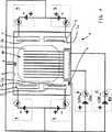
図面を参照しながら、本発明の好適な実施形態を以下にさらに詳細に説明するが、これはあくまでも例示としてのものに過ぎない。図1は、PVDコーティング装置の電気供給源の模式的な回路図である。図2は、図1に示した電気供給源の変形を示す模式的な回路図である。
図1は、PVDコーティング装置の電気供給源を示す模式的な回路図である。この図に示した実施形態のPVDコーティング装置は、コーティング・チャンバ1を持つ。コーティング・プロセス中、作用ガスは、ガス接続部(図示せず)を通して、このチャンバ1に供給される。
作用ガスとしては、例えば、アルゴンのような希ガスを使用することができる。
さらに、反応性ガスが、ガス接続部(図示せず)を通して、チャンバ1内に供給される。反応性ガスとしては、窒化物、炭化物および炭素窒化物を形成するために使用することができる、窒素や、CH4、C2H2またはC2H6のような炭素を含むガスを使用することができる。
コーティング・プロセスの最初のところで、作用ガス/反応性ガスの混合気体内でプラズマ(P)が発生する。そのため、コーティング装置は、二つのアノード2および四つのターゲット・カソード3を持ち、ターゲット・カソード3は、対向するペアの形で配置されていて、アノード2は、本質的には相互に向き合う形で、相互に対向するターゲット・カソード3間の中間のスペースに対して横向きに配置されている。
例示としての実施形態の場合には、アノード2は、欧州特許第0434797号が開示している高イオン化アノードである。イオン化プロセスに効果のあるアノード領域を設定ターゲット・カソード電力と整合させるために、アノードは部分的にダイヤフラムでカバーされているが、上記ダイヤフラムは導電性のものである。このダイヤフラムは、チャンバ壁部8と同じ電位を持つ。このようなアノード2は、プラズマ(P)の高いイオン化に特に適している。しかし、基本的には、アノード内部に能動アノード領域が形成されていれば十分である。
なお、ターゲット・カソードは、いわゆる不平衡マグネトロンであることが好ましい。
アノード2は、ターゲット・カソード3に対して正のバイアスが印加される。そのため、各ターゲット・カソード3は、それぞれ、カソード電圧源4に接続している。電圧源4は、それぞれ、約500ボルトの第一の電圧UKを供給する。この数値は、コーティング・プロセス中、すなわち、プラズマ(P)の発生後維持される。
プラズマ(P)が発生すると、チャンバ1内にプラズマの雲ができる。このプラズマの雲は、とりわけ、作用ガスのイオンを含んでいる。これらの作用ガスイオンは、アノード2とターゲット・カソード3との間の電界により、特にプラズマの雲とターゲット・カソード3との間の電位勾配によりターゲット・カソードの方向に加速される。
ターゲット・カソード3は、ターゲット材料5を含んでいるが、図の実施形態の場合には、このターゲット材料は、チタン/アルミニウム混合ターゲット5a、5bである。しかし、銅、プラチナ、クローム、ニッケルまたは他の金属を含むターゲット、およびセラミック材料のような非導体材料も使用することができる。その場合には、プラズマ(P)を維持するために、交流電界が必要になる。
このターゲット材料5には、作用ガスイオンが衝突する。すなわち、スパッタリング・プロセスが行われる。このプロセスにより、ターゲット材料5が、ターゲット・カソード3から原子の形またはイオンの形で遊離する。その場合、ターゲット・カソードを離れた直後で、イオン化されているターゲット材料の割合は約5%になる。
このタイプはイオンの量が少ないので、平滑な表面構造を有する高い密度と緻密さを特徴とするコーティング構造体を形成することはできない。
イオン化の程度を増大するために、コーティング装置は、最大12キロワットの電力で、500ボルトのカソード/アノード電圧で動作するカソード電圧源の他に、さらに二つの電圧源6、7を持つ。その設定電圧は、ターゲット材料のイオン化の程度を必要なだけ増大させるのに決定的な影響を持つ。これらの電圧源6、7は、最高6キロワットの電力で動作する。すべての電圧源4、6および7は、コーティング・プロセスを精密に最適化することができるように調整することができる。
電圧源6は、アノード2に特定の電位、すなわち、チャンバ1の壁部8に対して正のアノード電位を供給する。電圧源6は、50〜250ボルトの第二の電圧UAnを供給する。それ故、アノード2は、第二の電圧UAnにより、接地されているチャンバ壁部8に対して正にバイアスされる。
電圧源7は、第三の電圧UBi、いわゆるバイアス電圧を供給するが、その正の電極は、アノード2に接続している。この電圧源7の負の電極は、基板テーブル9に接続される。基板テーブル9は、一組の基板10がターゲット材料3から約40ミリ離れた場所に配置されるように、また、ターゲット・カソード3とアノード2との間の距離が250ミリの範囲内になるように、チャンバ1内に配置される。
基板テーブル9は、基板10のセットに電気的に接続している。コーティング・プロセスを行うためには、アノード電位が基板電位に対してより正の電圧になる必要がある。それ故、負の電圧を供給する電圧源7は、上記一組の基板10の電位が、アノード2の電位より、もっと負の最高で800ボルトとなるように設定される。
この場合、電圧源6および7の両方を対称的に動作させることができる。その場合、チャンバ壁部8の電位と上記一組の基板10の電位とは同じである。これら二つの電圧源6、7が非対称的な動作をする場合には、アノード電位は、基板の電位よりさらに高い正の電位を持つ。そして、基板電位に対してチャンバ電位をもっと正の電位にすることが好ましい。これにより、ターゲット・イオンは、基板の方向に引き寄せられ、チャンバ壁部8上で再結合しない。しかし、チャンバの電位を基板の電位に対して負にすることもできる。
それ故、基準電位ゼロに接地されているチャンバ1に対する通常の電位の数値は、アノード2の場合は、+50ボルトから+250ボルトであり、ターゲット・カソード3の場合には、−350ボルトから−750ボルトであり、基板テーブル9/基板10の電位は、+200ボルトから−1,000ボルトである。この場合、満足させなければならない条件は、基板10の電位がアノード2の電位より、もっと負の電位でなければならないことと、アノード2とターゲット・カソード3との間の電位差を各コーティング・プロセス(材料に依存する)に対して最適化させなければならないことであり、特に各プラズマを維持するために最適化させなければならないことである。
電圧源6および7を非対称的に動作させ、且チタン/アルミニウム混合ターゲット5a、5bを含む図示の実施形態の場合には、アノード電位は+180ボルトであり、基板電位は−20ボルトであり、チャンバ電位は0ボルトであり、カソード電位は−320ボルトである。
上記一組の基板10は、ターゲット・カソード3とアノード2との間に形成されたプラズマの雲の中に配置される。このプラズマの雲の特徴は、供給電圧UK、UAnおよびUBiにより、基板10に対して約+130ボルトの電位となっていることである。プラズマの雲のこの電位は、通常、ターゲット材料のイオンが、蒸着用のプラズマ(P)から上記一組の基板10へ移動するような数値でなければならない。
例示としての実施形態は、0ボルトから130ボルトの領域内に、四つのターゲット・カソード3と、二つのアノード2とを持つ。この場合、全カソードの最高電力は32キロワットであり、最高バイアス電流は30アンペアであり、最高アンペア電流は45アンペアに設定される。
基板10のタイプが何であれ、本発明の電気接続により、大きな割合のターゲット材料イオンが発生するように、チャンバ1内に電位降下が起こる。電圧源6、7の動作により、そうでない場合には、チャンバ壁部8上で、イオン、プラズマ(P)からの準安定粒子および電子を再結合化する大きな割合の電荷キャリヤが、カソード3から基板10へ移動中に、ターゲット材料の原子をイオン化するために供給される。アノード2とターゲット・カソード3との間の上記電気的接続により、ターゲット・カソード3の前面の電荷キャリヤ密度が濃くなり、上記一組の基板10に移動している間に、スパッタリングされたターゲット・カソード材料がイオン化される。スパッタリングされたターゲット・カソード材料の大きな割合のイオンにより、またチャンバ1内の上記電位プロファイルにより、基板10が三次元のものであっても、上記一組の基板10上において、基板10のジェット研摩又は研削された面上に、密度が高く緻密な層構造体、いわゆる小さな波模様の構造体を形成することができる。
上記層構造体は、反応性ガスを使用した場合には、ターゲット材料と反応性ガスとの間の化学反応による、チャンバ1内の雰囲気に含まれる材料からなる。例を挙げて説明すると、上記一組の基板10のTiAlNを含むコーティングの場合には、化学反応が、チャンバ1内で、ターゲット材料であるチタンおよびアルミニウムと反応性ガスである窒素との間で起こる。
層構造体の特性を最大限度に均一なものにするために、基板10を、ターゲット・カソード3の間で最大四本の回転軸を中心にして回転することができる。
図2は、図1に示した電源の変形例の模式的な回路図である。
図1と比較すると、図2は、さらに、電圧源7と基板テーブル9との間に接続しているパルス装置11を含む。上記パルス装置11は、例えば、350ボルトの最大バイアス電圧が基板テーブル9に供給され、基板テーブル9とプラズマ(P)との間の平均電位差が、図1の実施形態の場合のように、約130ボルトになるように設定される。
パルス装置11を設置することにより、基板10の縁部に対する平均イオン電流が大きくなるので、縁部のコーティングを抑制する周知の再スパッタリング効果を打ち消すことにより、良好なコーティングを行うことができる。
図2の構造の残りの部分は、図1の構造と同じである。より詳細に説明すると、アノード電位UAnも同じである。
パルス装置11を含むPVDコーティング装置のもう一つの実施形態(図示せず)は、アノード2の電位がパルス状に変化するように構成されている。この場合、パルス装置11は、図1の電気的接続を維持しながら、電圧源6とアノード2との間に接続している。上記一組の基板10上では、電圧UBiに対して、図1の電気的接続に従って選択される数値のオフセット電位が発生する。
パルス装置を含む両方の実施形態の場合、パルス動作の周波数は、0.5〜1MHz、好適には、0.1〜10Hzの領域である。
上記説明を補足すると、イオン化の程度を増大するために、アーク蒸発装置、低電圧アーク、中空電極、イオン源等を、PVDコーティング装置で、蒸発装置またはイオン源として使用することができる(ハイブリッド方法)。
PVDコーティング装置用の上記各実施形態を使用すれば、下記のステップを含むPVDコーティング方法を行うことができる。
真空にすることができるチャンバ内にスパッタリング・プロセスが行われる少なくとも一つのターゲット・カソードと、少なくとも一つのアノードおよび基板と、基板に電気的に接続している基板ホルダーとを配置するステップと、
少なくとも一つのガス供給接続部を通して、上記チャンバを作用ガスおよび/または反応性ガスで充填するステップと、
基板が配置された状態でプラズマを発生するため、ターゲット・カソードに、アノードに対して負の電位を供給するために、第一の電圧を供給するステップと、
アノードに、チャンバ壁部に対して正の電位を供給するために、第二の電圧を供給するステップと、
基板に、アノードよりさらに負の電位を供給する第三の電圧を供給するステップと、
予め定めたコーティング時間が経過した後で、チャンバから基板を取り出すステップ。
この方法は、非常に優れた層特性(小さな波模様の表面)を持つコーティング基板を製造する為に使用することができる。上記コーティング・プロセスを実行するには約8時間かかる。8ミリの孔部を有する基板材料を用いて最大860個分を同時にコーティングすることができる。
【図面の簡単な説明】
【図1】PVDコーティング装置の電気供給源の模式的な回路図である。
【図2】図1に示した電気供給源の変形を示す模式的な回路図である。[0001]
BACKGROUND OF THE INVENTION
The present invention relates to a PVD coating apparatus including a chamber that can be evacuated.
[0002]
[Prior art]
The apparatus comprises at least one gas supply connection for holding at least one target cathode, at least one anode, and at least one substrate that is subjected to a sputtering process and is held. At least one substrate holder in electrical connection with each substrate is disposed, and in order to form a plasma with the substrate disposed, a negative potential relative to the anode is applied to the target cathode. A control device having a first voltage output connected to supply a first voltage for supplying and further supplying a positive potential to the anode against the chamber wall. Having a second voltage output connected to supply a second voltage.
The present invention also relates to a PVD coating method for producing a coated substrate. EP 04349797 discloses such a PVD coating apparatus.
Known PVD coating equipment is typically used to coat all kinds of tools and parts in order to make the surface functional and possibly beautiful. In the case of tools, for example, coating with a metal-containing component such as TiAlN is very often performed.
One well-known technique for coating is a method of depositing agglomerates from the gas phase. In the case of this technique, various devices are used, but each device is optimized for a particular method. An apparatus in which the coating is performed with ionized atoms obtained in large proportions from the plasma is particularly advantageous when performing the coating.
In a coating apparatus in which a large proportion of metal atoms is generated in the plasma, the metal material usually evaporates from the target cathode, and the material evaporated at a large proportion is ionized. In this type of device, the target cathode material first melts and then vaporizes. The rate at which the evaporated raw material is ionized is high.
[0003]
[Problems to be solved by the invention]
However, with this type of known device where the target cathode material melts, it has been found that there is a drawback that the gas phase is not homogeneous while the alloy is evaporating in the gas phase and particulates are formed. Yes. Thus, the condensed coating material contains so-called particulates and / or the coating composition is not homogeneous.
Other known coating devices are configured to perform cathode sputtering using a magnetron magnetic field for the purpose of improving ionization efficiency to evaporate the target cathode material. In this case, the raw material changes directly from solid to vapor without going through a molten state.
However, the cathode sputtering apparatus has a drawback that the evaporated material is only slightly ionized. Plasma consists of a very large proportion of evaporated neutral particles (ionization rate about 5%), ionized gas particles from the working gas used to knock out target atoms and ions and to form the plasma, It consists of ionized gas particles from a reactive gas combined with the cathode material. If the surface is technically rough, especially in the case of a polished or ground rough surface, the coatings deposited from these plasmas have a good adhesion, hardness, structure and surface shape (smoothness). And color). In the case of such a substrate surface, it has been impossible until now to form a surface coating with a so-called small wave pattern (dimple) characterized by a smooth structure, a high density and a dense structure.
WO 91/00374 discloses a process and apparatus for coating a substrate using both arc discharge deposition and cathode deposition. In this case, arc discharge deposition is performed before cathode deposition. The circuit of WO 91/00374 includes a voltage source connected between the cathode and the chamber, a voltage source connected between the cathode and the anode, and a voltage source for supplying a bias voltage to the substrate. EP0558061A1 discloses almost the same device.
EP 0 767 595 A1 discloses an apparatus for performing only arc discharge deposition. The apparatus can include one voltage source with the cathode continuously connected to the voltage source, and preferably the anode and substrate connected to the remaining electrodes of the voltage source.
[0004]
[Means for solving the problems]
An object of the present invention is to provide a PVD coating apparatus based on this prior art, in which the target cathode material is used for coating a substrate which is a normal type using evaporation from a solid and does not go through a molten state and is a tool. It is to develop further. In this case, a large proportion of the raw material is agglomerated on the substrate as a tool with a high adhesive force, and is technically applicable to a substrate having a surface roughened by grinding or jet polishing.
The above object is achieved by a normal type device having a third voltage output connected to apply a third voltage, in which the control device supplies a more negative potential than the anode potential to the substrate. Is done.
The effect of doing so is that during operation of the PVD coating apparatus in the chamber, another electrode, i.e. the substrate, is at a certain potential in the plasma. This electrode is placed in the plasma to ensure that an advantageous potential profile is created in the chamber. More specifically, the second voltage, ie, the anode voltage, allows the current flowing through the substrate to be set, while maintaining the third voltage, ie, the substrate voltage or bias voltage, constant. Can do. Therefore, the coating state on the substrate can be optimized very easily.
This electrical connection configuration also has a decisive influence on the electron density distribution in the chamber. Since the substrate potential is more negative than the anode potential, in order to maintain the plasma, the electron trajectory extends from the target cathode to the anode and also promotes ionization of the metal atoms emitted from the target cathode. Results in a dominant extension from the target cathode to the substrate. The reason why ionization is promoted is that the movement path of the metal atoms from the target cathode to the substrate coincides with the latter part of the electron orbit.
Within the chamber, an ionization efficiency of 50% or more can be achieved for the emitted target metal atoms with the potential profile set according to the invention. As a result, the sputtering method using this coating apparatus can form a deposition layer having a small wavy surface on the substrate even when the substrate surface is rough due to, for example, grinding or jet polishing. A suitable degree of ionization can be performed. At the target cathode, power densities of up to 45 W / cm2 can be achieved, and the discharge current is significantly increased compared to the prior art.
The potential profile in the chamber also has another consequence that the potential of the plasma generated between the target cathode and anode around the substrate is basically more positive than the substrate potential. The effect is, for example, that ions from the plasma in this region of the chamber can move with a high probability in the direction of the substrate and can be deposited there.
The arrival of electrons to the chamber wall is further hindered, so there is no power to ionize the metal atoms there. For this purpose, it is preferred that the substrate has the same potential as the target cathode or is positively biased with respect to the target cathode to attract electrons toward the substrate so as to ionize the target material. However, the potential of the target / cathode can be made more positive than the potential of the substrate.
Multiple anodes and target cathodes can also be set up in a symmetrical arrangement so that the substrate is located in the plasma during the coating process.
For example, the substrate is a cutting tool and is coated with a hard material.
Preferably, the second and third voltages are set so that the positive potential of the anode relative to the chamber wall is less than the positive potential of the anode relative to the substrate so that the substrate can be placed in the vicinity of the target cathode. It is preferable.
In the case of embodiments of the present invention, the optimization of the electron density distribution in the chamber in front of the target cathode is particularly efficient. Due to the negative bias voltage of the substrate relative to the anode and due to the proximity of the target cathode and the substrate, the proportion of electron trajectories reaching the substrate further increases, so that the metal atoms from the target cathode Ionization is improved.
Preferably, when the first, second and third voltages are appropriately set and a plasma is generated between the target cathode and the anode in the region where the substrate is placed, the floating potential is the substrate potential. Higher, about 40-400 volts, preferably 130 volts is preferred.
This ensures that a very large percentage of ions flow from the plasma in the substrate region towards the substrate and can be deposited on the substrate to form a coating. Therefore, ion loss due to ion recombination on the chamber walls is minimal.
In the preferred embodiment, the first voltage is set so that the anode is at a potential up to about 800 volts above the potential of the target cathode. The second voltage is set at a potential such that the anode is about 50-250 volts positive from the chamber wall potential. On the other hand, the third voltage is preferably set so that the anode is within 800 volts, particularly 100 to 200 volts positive, from the substrate potential.
The above numerical range of potential differences between the anode, the target cathode, the chamber wall and the substrate has been found to be a very favorable value experimentally. When setting the potential, especially between the anode and cathode, each characteristic of the target material must be taken into account. In particular, its magnetic properties must be taken into account.
The ratio of the distance between the target cathode and the substrate to the distance between the target cathode and the anode is preferably about 1: 5.
This distance ratio determines the geometric relationship of the electrode, target cathode, substrate, chamber wall and anode. Its characteristics lie in the particularly preferred profile of the equipotential lines that determine the orbitals of the charge carriers, in particular the electron density distribution.
For example, the substrate holder should be positioned so that the substrate is approximately 40 mm from the target cathode and the distance between the target cathode and anode is in the range of 250 mm. Can do.
This method allows the PVD coating system to be particularly compact. More specifically, since the distance from the target cathode to the substrate is short, the coating speed of the substrate is very high. Thus, the speed is increased, and the coating cost is reduced.
Preferably, the control device has a voltage source assigned to each of the three voltages. The first voltage source is connected between the anode and the target cathode, the second voltage source is connected between the anode and the chamber wall, and the third voltage source is connected between the anode and the substrate. Connected between. In this case, the substrate current is set by acting on the plasma using the second voltage source, while holding the setting of the third voltage source changes the setting of the second voltage source, And even if the substrate current changes, the potential difference between the substrate and the anode is maintained.
In this case, any fluctuations in the anode potential that may occur can never affect the voltage difference between the anode and the target cathode, the voltage difference between the anode and the substrate, Therefore,Ru can be the operation of the PVD coating device morestable.
Three in the case of another example of the embodiment having the voltage source, the voltage source of the control device, can be only a voltage source of one supplying the first charge between the anode and the target cathode For the second and third voltages, each variable resistor connected in parallel to the voltage source can be used. The variable resistor is set so that a potential necessary for the anode and the substrate appears in each tap.
Nevertheless, it is important for the invention, whatever the electrical connection method,Ru der that the potential profile within the chamber ismaintained.
[0005]
DETAILED DESCRIPTION OF THE INVENTION
Preferred embodiments of the present invention will be described in more detail below with reference to the drawings, but this is merely an example. FIG. 1 is a schematic circuit diagram of an electric power source of a PVD coating apparatus. FIG. 2 is a schematic circuit diagram showing a modification of the electricity supply source shown in FIG.
FIG. 1 is a schematic circuit diagram showing an electric power source of a PVD coating apparatus. The PVD coating apparatus of the embodiment shown in this figure has a
As the working gas, for example, a rare gas such as argon can be used.
Further, a reactive gas is supplied into the
At the beginning of the coating process, a plasma (P) is generated in the working gas / reactive gas mixture. Therefore, the coating apparatus has two
In the exemplary embodiment,
The target cathode is preferably a so-called unbalanced magnetron.
A positive bias is applied to the
When plasma (P) is generated, a plasma cloud is formed in the
The
The
Since this type has a small amount of ions, it is not possible to form a coating structure characterized by a high density and density with a smooth surface structure.
To increase the degree of ionization, the coating apparatus has two
The
The voltage source 7 supplies a third voltage UBi , the so-called bias voltage, whose positive electrode is connected to the
The substrate table 9 is electrically connected to a set of
In this case, both
Therefore, typical potential values for
In the illustrated embodiment where
The set of
The exemplary embodiment has four
Whatever the type of
When the reactive gas is used, the layer structure is made of a material contained in the atmosphere in the
In order to maximize the properties of the layer structure, the
FIG. 2 is a schematic circuit diagram of a modification of the power supply shown in FIG.
Compared to FIG. 1, FIG. 2 further includes a pulse device 11 connected between the voltage source 7 and the substrate table 9. The pulse device 11 is supplied with a maximum bias voltage of, for example, 350 volts to the substrate table 9 so that the average potential difference between the substrate table 9 and the plasma (P) is approximately as in the embodiment of FIG. Set to 130 volts.
By installing the pulse device 11, the average ionic current with respect to the edge of the
The rest of the structure of FIG. 2 is the same as the structure of FIG. More specifically, the anode potential UAn is the same.
Another embodiment (not shown) of the PVD coating apparatus including the pulse device 11 is configured such that the potential of the
For both embodiments including a pulse device, the frequency of the pulse operation is in the region of 0.5-1 MHz, preferably 0.1-10 Hz.
Supplementing the above description, in order to increase the degree of ionization, arc evaporators, low voltage arcs, hollow electrodes, ion sources, etc. can be used in PVD coating devices as evaporators or ion sources (hybrid method). ).
If each said embodiment for PVD coating apparatuses is used, the PVD coating method including the following steps can be performed.
Placing at least one target cathode to be subjected to a sputtering process in a chamber capable of being evacuated, at least one anode and a substrate, and a substrate holder electrically connected to the substrate;
Filling the chamber with working gas and / or reactive gas through at least one gas supply connection;
Supplying a first voltage to the target cathode to supply a negative potential to the anode to generate plasma with the substrate disposed;
Supplying a second voltage to the anode to provide a positive potential relative to the chamber wall;
Supplying a substrate with a third voltage for supplying a more negative potential than the anode;
Removing the substrate from the chamber after a predetermined coating time has elapsed;
This method can be used to produce a coated substrate with very good layer properties (small wavy surface). It takes about 8 hours to perform the coating process. A maximum of 860 substrates can be coated simultaneously using a substrate material having 8 mm holes.
[Brief description of the drawings]
FIG. 1 is a schematic circuit diagram of an electric power source of a PVD coating apparatus.
FIG. 2 is a schematic circuit diagram showing a modification of the electricity supply source shown in FIG.
Claims (5)
Translated fromJapanese少なくとも一つのガス供給接続部を備え、
スパッタリング・プロセスを受ける少なくとも一つのターゲット・カソード(3)と、少なくとも一つのアノード(2)と、少なくとも一つの、工具である基板(10)を保持するためのものであって、保持されている工具である各基板(10)に電気的に接続している少なくとも一つの工具用の基板ホルダー(9)が配置されていて、
前記工具である少なくとも一つの基板(10)が配置された状態でプラズマ(P)を形成するために、前記少なくとも一つのターゲット・カソード(3)に、前記少なくとも一つのアノード(2)に対して負の電位を供給するための第一の電圧を制御するように、前記少なくとも一つのターゲット・カソード(3)と前記少なくとも一つのアノード(2)との間に接続している装置(4)を含み、
前記少なくとも一つのアノード(2)に、チャンバ壁部(8)に対して正の電位を供給するための第二の電圧を制御するように、前記少なくとも一つのアノード(2)と前記チャンバ壁部(8)との間に接続している装置(6)を持ち、
前記少なくとも一つの基板(10)と前記少なくとも一つのアノード(2)との間に接続した装置(7)を持ち、前記装置(7)は前記少なくとも一つの基板(10)に、前記少なくとも一つのアノード(2)の電位より負の電位を供給する第三の電圧を制御し、
前記第二の電圧を変化させて基板(10)を流れる電流を変えることができる一方、前記第三の電圧を保持することにより基板(10)とアノード(2)との間の電位差を維持することができ、
以って、工具である基板のコーティングに用いることを特徴とするPVDコーティング装置。A PVD coating apparatus comprising a chamber (1) capable of being evacuated,
Comprising at least one gas supply connection,
At least one target cathode (3) subjected to a sputtering process, at least one anode (2), and at least one tool for holding a substrate (10), which is held. A substrate holder (9) for at least one tool electrically connected to each substrate (10) as a tool is arranged;
In order to form a plasma (P) in a state where at least one substrate (10) as the tool is disposed, the at least one target cathode (3) is in contact with the at least one anode (2). tocontrol the first voltage for supplyingthe negative potential, the at least onedevice connected between the target cathode and (3) said at least one anode (2) and(4) Including
The at least one anode (2) and the chamber wall soas tocontrol a second voltage for supplying a positive potential to the chamber wall (8) to the at least one anode (2). Hold thedevice (6) connected between (8) and
Before SL has at leastdevice connectedbetween one of saidsubstrate (10) at least one anode (2)(7),the device (7) said at least onesubstrate (10), at leastControlling a third voltage to supply a negative potential from the potential of one anode (2);
The current flowing through the substrate (10) can be changed by changing the second voltage, while maintaining the potential difference between the substrate (10) and the anode (2) by maintaining the third voltage. It is possible,
Therefore, a PVD coating apparatus characterized by being used for coating a substrate as a tool.
Applications Claiming Priority (5)
| Application Number | Priority Date | Filing Date | Title |
|---|---|---|---|
| DE19715535 | 1997-04-14 | ||
| DE19754821.0 | 1997-12-10 | ||
| DE19754821ADE19754821A1 (en) | 1997-04-14 | 1997-12-10 | Method and device for a PVD coating |
| DE19715535.9 | 1997-12-10 | ||
| PCT/EP1998/002100WO1998046807A1 (en) | 1997-04-14 | 1998-04-09 | Method and device for pvd coating |
Publications (3)
| Publication Number | Publication Date |
|---|---|
| JP2001518982A JP2001518982A (en) | 2001-10-16 |
| JP2001518982A5 JP2001518982A5 (en) | 2005-11-10 |
| JP4792571B2true JP4792571B2 (en) | 2011-10-12 |
Family
ID=7826463
Family Applications (1)
| Application Number | Title | Priority Date | Filing Date |
|---|---|---|---|
| JP54347198AExpired - LifetimeJP4792571B2 (en) | 1997-04-14 | 1998-04-09 | PVD coating equipment |
Country Status (2)
| Country | Link |
|---|---|
| JP (1) | JP4792571B2 (en) |
| DE (2) | DE19754821A1 (en) |
Families Citing this family (3)
| Publication number | Priority date | Publication date | Assignee | Title |
|---|---|---|---|---|
| DE102008060838A1 (en) | 2008-12-05 | 2010-06-10 | Zounek, Alexis, Dr. | Coating substrates, comprises generating plasma with positively charged ion that is accelerated on substrate by negative bias potential, and reducing and/or compensating positive loading of substrate by irradiating substrate with electron |
| US11155921B2 (en) | 2015-11-05 | 2021-10-26 | Bühler Alzenau Gmbh | Device and method for vacuum coating |
| JP2023027480A (en)* | 2021-08-17 | 2023-03-02 | 株式会社東芝 | Plasma source and switch device |
Family Cites Families (4)
| Publication number | Priority date | Publication date | Assignee | Title |
|---|---|---|---|---|
| JPH0230384B2 (en)* | 1985-04-05 | 1990-07-05 | Hitachi Ltd | SUPATSUTAHOHOOYOBISOCHI |
| JPH0834002B2 (en)* | 1988-07-15 | 1996-03-29 | 三菱化学株式会社 | Method of manufacturing magnetic recording medium |
| JPH02225665A (en)* | 1989-02-27 | 1990-09-07 | Fuji Electric Co Ltd | Magnetron sputtering device |
| DE69329161T2 (en)* | 1992-02-27 | 2001-01-11 | Hauzer Industries B.V., Venlo | Improvements in physical vapor deposition processes |
- 1997
- 1997-12-10DEDE19754821Apatent/DE19754821A1/ennot_activeCeased
- 1998
- 1998-04-09DEDE69808267Tpatent/DE69808267T2/ennot_activeExpired - Lifetime
- 1998-04-09JPJP54347198Apatent/JP4792571B2/ennot_activeExpired - Lifetime
Also Published As
| Publication number | Publication date |
|---|---|
| DE69808267T2 (en) | 2003-03-06 |
| DE19754821A1 (en) | 1998-10-15 |
| JP2001518982A (en) | 2001-10-16 |
| DE69808267D1 (en) | 2002-10-31 |
Similar Documents
| Publication | Publication Date | Title |
|---|---|---|
| EP0975818B1 (en) | Method and device for pvd coating | |
| US4992153A (en) | Sputter-CVD process for at least partially coating a workpiece | |
| US5294322A (en) | Electric arc coating device having an additional ionization anode | |
| US9941102B2 (en) | Apparatus for processing work piece by pulsed electric discharges in solid-gas plasma | |
| US9812299B2 (en) | Apparatus and method for pretreating and coating bodies | |
| JP3652702B2 (en) | Linear arc discharge generator for plasma processing | |
| RU2461664C2 (en) | Method for deposition of electric insulating layers | |
| JP4208258B2 (en) | Method and apparatus for coating a workpiece | |
| EP0558061B1 (en) | Improvements in physical vapour deposition processes | |
| JPH06256944A (en) | Substrate treating device | |
| US20140238852A1 (en) | Cylindrical evaporation source | |
| SG186722A1 (en) | Arc deposition source having a defined electric field | |
| TWI296813B (en) | Improvements in and relating to magnetron sputtering | |
| JP4792571B2 (en) | PVD coating equipment | |
| US6083356A (en) | Method and device for pre-treatment of substrates | |
| JP7026464B2 (en) | Method for depositing layers using magnetron sputtering equipment | |
| US10083822B2 (en) | Physical vapour deposition coating device as well as a physical vapour deposition method | |
| JP3555033B2 (en) | Apparatus for coating a substrate with a material vapor under negative pressure or vacuum | |
| JPH0860343A (en) | Vacuum deposition device | |
| JPH06145979A (en) | Film forming device | |
| JP2000226648A (en) | METHOD FOR EVAPORATING TiB2 | |
| JPH0754147A (en) | Dynamic mixing device | |
| JPH1150245A (en) | Sputter deposition apparatus and sputtering target | |
| JPH05287516A (en) | Thin film vapor deposition device and thin film forming method using this device | |
| MXPA00002589A (en) | Tool having a protective layer system |
Legal Events
| Date | Code | Title | Description |
|---|---|---|---|
| A521 | Request for written amendment filed | Free format text:JAPANESE INTERMEDIATE CODE: A523 Effective date:20050323 | |
| A621 | Written request for application examination | Free format text:JAPANESE INTERMEDIATE CODE: A621 Effective date:20050323 | |
| A131 | Notification of reasons for refusal | Free format text:JAPANESE INTERMEDIATE CODE: A131 Effective date:20070828 | |
| A601 | Written request for extension of time | Free format text:JAPANESE INTERMEDIATE CODE: A601 Effective date:20071109 | |
| A602 | Written permission of extension of time | Free format text:JAPANESE INTERMEDIATE CODE: A602 Effective date:20071221 | |
| A601 | Written request for extension of time | Free format text:JAPANESE INTERMEDIATE CODE: A601 Effective date:20071218 | |
| A602 | Written permission of extension of time | Free format text:JAPANESE INTERMEDIATE CODE: A602 Effective date:20080204 | |
| A601 | Written request for extension of time | Free format text:JAPANESE INTERMEDIATE CODE: A601 Effective date:20080121 | |
| A602 | Written permission of extension of time | Free format text:JAPANESE INTERMEDIATE CODE: A602 Effective date:20080303 | |
| A521 | Request for written amendment filed | Free format text:JAPANESE INTERMEDIATE CODE: A523 Effective date:20080227 | |
| A02 | Decision of refusal | Free format text:JAPANESE INTERMEDIATE CODE: A02 Effective date:20080729 | |
| A521 | Request for written amendment filed | Free format text:JAPANESE INTERMEDIATE CODE: A523 Effective date:20081121 | |
| A521 | Request for written amendment filed | Free format text:JAPANESE INTERMEDIATE CODE: A821 Effective date:20081125 | |
| A911 | Transfer to examiner for re-examination before appeal (zenchi) | Free format text:JAPANESE INTERMEDIATE CODE: A911 Effective date:20090115 | |
| A912 | Re-examination (zenchi) completed and case transferred to appeal board | Free format text:JAPANESE INTERMEDIATE CODE: A912 Effective date:20090226 | |
| A601 | Written request for extension of time | Free format text:JAPANESE INTERMEDIATE CODE: A601 Effective date:20110411 | |
| A602 | Written permission of extension of time | Free format text:JAPANESE INTERMEDIATE CODE: A602 Effective date:20110414 | |
| A601 | Written request for extension of time | Free format text:JAPANESE INTERMEDIATE CODE: A601 Effective date:20110509 | |
| A602 | Written permission of extension of time | Free format text:JAPANESE INTERMEDIATE CODE: A602 Effective date:20110512 | |
| A521 | Request for written amendment filed | Free format text:JAPANESE INTERMEDIATE CODE: A523 Effective date:20110517 | |
| A01 | Written decision to grant a patent or to grant a registration (utility model) | Free format text:JAPANESE INTERMEDIATE CODE: A01 | |
| A61 | First payment of annual fees (during grant procedure) | Free format text:JAPANESE INTERMEDIATE CODE: A61 Effective date:20110630 | |
| R150 | Certificate of patent or registration of utility model | Free format text:JAPANESE INTERMEDIATE CODE: R150 | |
| FPAY | Renewal fee payment (event date is renewal date of database) | Free format text:PAYMENT UNTIL: 20140805 Year of fee payment:3 | |
| R250 | Receipt of annual fees | Free format text:JAPANESE INTERMEDIATE CODE: R250 | |
| R250 | Receipt of annual fees | Free format text:JAPANESE INTERMEDIATE CODE: R250 | |
| R250 | Receipt of annual fees | Free format text:JAPANESE INTERMEDIATE CODE: R250 | |
| R250 | Receipt of annual fees | Free format text:JAPANESE INTERMEDIATE CODE: R250 | |
| EXPY | Cancellation because of completion of term |