JP4792180B2 - 半導体デバイスの製造方法、基板処理方法および基板処理装置 - Google Patents
半導体デバイスの製造方法、基板処理方法および基板処理装置Download PDFInfo
- Publication number
- JP4792180B2 JP4792180B2JP2001231330AJP2001231330AJP4792180B2JP 4792180 B2JP4792180 B2JP 4792180B2JP 2001231330 AJP2001231330 AJP 2001231330AJP 2001231330 AJP2001231330 AJP 2001231330AJP 4792180 B2JP4792180 B2JP 4792180B2
- Authority
- JP
- Japan
- Prior art keywords
- region
- monogermane
- substrates
- substrate processing
- reactor
- Prior art date
- Legal status (The legal status is an assumption and is not a legal conclusion. Google has not performed a legal analysis and makes no representation as to the accuracy of the status listed.)
- Expired - Lifetime
Links
Images


Landscapes
- Chemical Vapour Deposition (AREA)
Description
【発明の属する技術分野】
本発明は、半導体デバイスの製造方法および基板処理装置に関し、特に、減圧CVD法(化学気相堆積法)によって、ポリまたはアモルファスシリコンゲルマニウムを成膜する半導体デバイスの製造方法、基板処理方法および基板処理装置に関する。
【0002】
【従来の技術】
IC、LSI等の半導体デバイスを製造する工程においては、減圧CVD法(化学気相堆積法)によって、基板上に薄膜を成膜することが行われている。そのような成膜工程の中の一つとして、減圧CVD法によって、ポリシリコンゲルマニウム膜をMOSトランジスタのゲート電極部分に形成することが試されている。
【0003】
従来、MOSトランジスタのゲート電極部分にはシリコンが使用されてきたが、近年のゲート絶縁膜の薄膜化に伴い、ゲートにバイアス電圧を印加した際のゲートの空乏化や、熱処理工程におけるドーパントの電極からチャネル部分への突き抜けが、デバイス特性を悪化させる大きな問題点となっていた。上記の問題点は、シリコンに代えてシリコンゲルマニウムを用いることによって大幅に改善されることが判明している。
【0004】
【発明が解決しようとする課題】
シリコンに代えてシリコンゲルマニウムを用いた場合、同じ成膜条件下(500℃)での成膜速度は、シリコンの場合と比較して、ゲルマニウム比率が20%の時で約6倍、ゲルマニウム比率が30%の時で約14倍に増加する。それに伴い、反応炉内を通過する際の反応ガスの消費量も増加し、その消費量の増加割合は、シリコンよりもゲルマニウムのほうが1cm3あたりの質量が2.3倍程度大きいため顕著である。ゲルマニウムの原料ガスであるモノゲルマンを反応炉下部から1本のノズルで炉内に供給した場合、モノゲルマンの消費により、反応炉内の上流側と下流側でガス濃度が顕しく異なり、膜厚およびゲルマニウム比率の面内・面間均一性は大幅に悪化する。
【0005】
本発明の目的は、上記課題を解決し、モノシランとモノゲルマンとを使用して、減圧CVD法によって、膜厚およびゲルマニウム比率の面内・面間均一性が良好なシリコンゲルマニウム膜を基板上に形成する半導体デバイスの製造方法、基板処理方法および基板処理装置を提供することである。
【0006】
【課題を解決するための手段】
上記課題を解決するために、本発明は、請求項1に記載のように、
反応炉内でボートにより複数枚の基板を垂直方向に積層支持する工程と、前記反応炉内にモノシランとモノゲルマンとを供給して、前記ボートにより積層支持された前記複数枚の基板上にシリコンゲルマニウム膜を成膜する工程と、を有し、前記シリコンゲルマニウム膜を成膜する工程では、前記モノゲルマンを長さの異なる複数本のノズルを用いて、前記反応炉内の前記複数枚の基板が存在する領域の垂直方向において異なる複数箇所から供給することを特徴とする半導体デバイスの製造方法を構成する。
【0007】
また、本発明は、請求項2に記載のように、
前記複数枚の基板が存在する領域は、トップ領域と、該トップ領域下方のセンタ領域と、該センタ領域下方のボトム領域とを含んでおり、前記シリコンゲルマニウム膜を成膜する工程では、前記モノゲルマンを前記トップ領域、前記センタ領域および前記ボトム領域のそれぞれの領域から供給することを特徴とする請求項1記載の半導体デバイスの製造方法を構成する。
また、本発明は、請求項3に記載のように、
前記シリコンゲルマニウム膜を成膜する工程では、前記モノゲルマンを前記反応炉内の前記複数枚の基板が存在する領域の下方からも供給することを特徴とする請求項1または2に記載の半導体デバイスの製造方法を構成する。
また、本発明は、請求項4に記載のように、
前記シリコンゲルマニウム膜を成膜する工程では、前記モノゲルマンを前記反応炉内の前記複数枚の基板が存在する領域の上流側からも供給することを特徴とする請求項1または2に記載の半導体デバイスの製造方法を構成する。
また、本発明は、請求項5に記載のように、
反応炉内でボートにより複数枚の基板を垂直方向に積層支持する工程と、前記反応炉内にモノシランとモノゲルマンとを供給して、前記ボートにより積層支持された前記複数枚の基板上にシリコンゲルマニウム膜を成膜する工程と、を有し、前記シリコンゲルマニウム膜を成膜する工程では、前記モノゲルマンを長さの異なる複数本のノズルを用いて、前記反応炉内の前記複数枚の基板が存在する領域の垂直方向において異なる複数箇所から供給することを特徴とする基板処理方法を構成する。
また、本発明は、請求項6に記載のように、
基板を処理する反応炉と、前記反応炉内にモノシランを供給する第1ノズルと、前記反応炉内にモノゲルマンを供給する第2ノズルと、前記反応炉内で複数枚の基板を垂直方向に積層支持するボートと、を有し、前記反応炉内にモノシランとモノゲルマンとを供給して、前記ボートにより積層支持された前記複数枚の基板上にシリコンゲルマニウム膜を成膜する処理を行う基板処理装置であって、前記第2ノズルは、前記モノゲルマンを前記反応炉内の前記複数枚の基板が存在する領域の垂直方向において異なる複数箇所から供給するよう、長さの異なる複数本のノズルで構成されることを特徴とする基板処理装置を構成する。
また、本発明は、請求項7に記載のように、
前記複数枚の基板が存在する領域は、トップ領域と、該トップ領域下方のセンタ領域と、該センタ領域下方のボトム領域とを含んでおり、前記第2ノズルは、前記モノゲルマンを前記トップ領域、前記センタ領域および前記ボトム領域のそれぞれの領域から供給するよう構成されることを特徴とする請求項6記載の基板処理装置を構成する。
また、本発明は、請求項8に記載のように、
前記第2ノズルは、前記モノゲルマンを前記反応炉内の前記複数枚の基板が存在する領域の下方からも供給するよう構成されることを特徴とする請求項6または7に記載の基板処理装置を構成する。
また、本発明は、請求項9に記載のように、
前記第2ノズルは、前記モノゲルマンを前記反応炉内の前記複数枚の基板が存在する領域の上流側からも供給するよう構成されることを特徴とする請求項6または7に記載の基板処理装置を構成する。
【0008】
【発明の実施の形態】
図1は、本発明の実施の形態例である基板処理装置の概要を示す。
【0009】
本発明の半導体デバイスの製造方法においては、反応ガスとしてモノシランとモノゲルマンとを使用し、反応炉11内において、減圧CVD法によって、基板であるウエハ4の上にシリコンゲルマニウム膜を成膜する半導体デバイスの製造方法において、図1に示すような長さの異なる多数本ノズル12a〜12eを通してモノゲルマンを炉内に供給することを特徴とする。
【0010】
本発明がなされる前の予備的考察において、膜厚およびゲルマニウム比率の面内・面間均一性を良好(3%以下)にするには、反応ガスの流れに沿って、成膜反応が始まる箇所から成膜が反応終わる箇所までの間で、モノシランガスおよびモノゲルマンガス、特に前述したようにモノゲルマンガスの消費を10%以下に保つことが必要であることが、経験上、認められている。
【0011】
モノゲルマンガスを反応炉11下部から1本のノズルで炉内に供給する形態で、モノゲルマンガスの消費を10%以下に保つために必要なモノゲルマン流量は、8インチウエハ用の内径26cmで高さが130cmの反応管内で、成膜される部分の表面積(反応管内壁およびウエハ表面)と実際の成膜速度(実験値)を考慮して見積もると、ゲルマニウム比率20%の場合約140sccmとなる。実際は安全のために反応ガスを10%程度に希釈して用いるので、1400sccmの希釈モノゲルマンを流すことになる。この時に必要なモノシラン流量はゲルマニウム比率20%で成膜温度が500℃の場合、約2800sccm(非希釈)である。ゲルマニウム比率をデバイス特性改善のためにもっと上げようとすると、前述したようにゲルマニウム比率を上げると成膜速度は速くなるので、ゲルマニウム比率30%の時に、モノゲルマンガスの消費を10%以下に保つために必要なモノゲルマンおよびモノシランの流量はそれぞれ500sccm(実際は5000sccmの希釈モノゲルマン)および5000sccm(非希釈)となり、このような大流量のガスを流して、反応炉内を一般的なプロセス圧力(30〜60Pa)にする場合には特大排気容量のポンプが必要であり現実的ではない。
【0012】
これらの計算結果から、多数本ノズルを用いてモノゲルマンを炉内に途中供給し、モノゲルマンの消費を、反応ガスの流れに沿って、成膜反応が始まる箇所から成膜が反応終わる箇所までの間で、10%以下に保つことが、膜厚およびゲルマニウム比率の面内・面間均一性が良好なシリコンゲルマニウム膜の形成を行う上で重要であるといえる。本発明は、このような考察に基づいてなされたものである。なお、このような条件下で形成されたシリコンゲルマニウム膜はポリシリコンゲルマニウム膜であるが、これとは異なる条件下ではアモルファスシリコンゲルマニウム膜が形成される場合もある。
【0013】
本発明に係る基板処理装置の一例として、反応ガスとしてモノシラン(SiH4)とモノゲルマン(GeH4)とを使用して、反応炉内でボートに複数枚のウエハを垂直方向に積層支持した状態で、炉体下部よりガスを導入し垂直方向に上昇させ、そのガスを用いたCVD法により、前記ウエハ上に薄膜を形成する減圧CVD装置の構造概略図を図1に示す。
【0014】
4ゾーンに分かれたヒータ6の内側に、反応炉11の外筒である石英製のアウターチューブ1およびアウターチューブ1内部の反応管であるインナーチューブ2が設置されており、この2種のチューブの間をメカニカルブースタポンプ7およびドライポンプ8を用いて真空引きしている。従って、インナーチューブ2内側に導入される反応ガスは、インナーチューブ2内を上昇し、2種のチューブ1、2の間を下降して排気される。ウエハ4が装填された石英ボート3はインナーチューブ2内に設置され、反応ガスにさらされた時に気相中およびウエハ4表面での反応により、ウエハ4上に薄膜が形成される。断熱板5はボート3と装置下部との間を断熱するためのものである。また、図1中、9はボート回転軸であり、10はステンレス製蓋である。
【0015】
なお、ボート3には、ウエハ4を支持するスロットが合計172個設けられており、一番下のスロットから数えて10スロット目まではダミーのウエハ4が、11から167スロット目までは製品のウエハ4が、168から172スロット目まではダミーのウエハ4が支持される。また、図1中のトップ領域、センタ領域、ボトム領域とは、それぞれ、129から167スロット目までの製品のウエハ4の存在する領域、37から128スロット目までの製品のウエハ4の存在する領域、11から36スロット目までの製品のウエハ4の存在する領域のことを示している。また、4つに分かれたヒータゾーンのうち、一番下のL(Lower)ゾーンは1スロット目より下側の、ウエハが殆ど存在しない領域に対応しており、下から二番目のCL(Center Lower)ゾーンは2から56スロット目までのダミーのウエハ4と製品のウエハ4とが混在する領域に対応しており、下から三番目すなわち上から二番目のCU(Center Upper)ゾーンは57から172スロット目までの製品のウエハ4とダミーのウエハ4とが混在する領域に対応しており、下から四番目すなわち一番上のU(Upper)ゾーンはそれより上側のウエハの存在しない領域に対応している。
【0016】
モノゲルマン(GeH4)を反応炉11内に供給する石英ノズル12a〜12eは長さが異なり、合計5本設けられており、12aはモノシラン(SiH4)を供給するノズルとともに炉口部(図中、左下)に設けられており、12b、12c、12d及び12eは、前記炉口部を通り、それぞれの噴出口が30スロット目、70スロット目、110スロット目及び150スロット目の位置に対応するように、設けられている。このような長さの異なる複数本ノズル12a〜12eを用いることによって、モノゲルマンを反応炉炉11内に途中供給することができる。
【0017】
また、断熱板5はLゾーンに対応するヒータ6よりも下側に設置される。
【0018】
本発明に係る半導体デバイスの製造方法の一例として、図1に示した基板処理装置を用いる成膜手順を図2に示す。
【0019】
まず反応炉11内を成膜温度に安定化させた後、基板であるウエハ4を装填したボート3を反応炉11内にロード(挿入)する。リアクター(反応炉11)内を排気し、ボート3やチューブ1、2に吸着した水分等を脱離させるためにN2パージを行う。リアクター(反応炉11)内リークチェックを行った後、モノシランとモノゲルマンの流量を設定し、反応炉11内にガスを流して圧力を安定化させ成膜を行う。成膜が終了したら配管内をN2でサイクルパージし、N2でリアクター内を大気圧まで戻す。大気圧に戻ったらボート3をアンロードし、ウエハ4を自然冷却する。最後にウエハ4をボート3から取り出す。
【0020】
[実施の形態例]
(複数本ノズルを用いたモノゲルマンの途中供給)
図1に例示した基板処理装置において、長さの異なる複数本ノズルを用いてモノゲルマンを反応炉内に途中供給することで、膜厚およびゲルマニウム比率の面内・面間均一性が良好なポリシリコンゲルマニウム膜の形成が可能となる。
【0021】
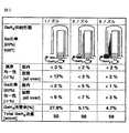
実際に実験を行った結果、得られた膜厚およびゲルマニウム比率の面内・面間均一性を、従来例をも含めて、モノゲルマン供給形態で比較して図3に示す。
【0022】
図3中、「1ノズル」は従来例に該当する形態であり、この場合に、モノゲルマンのノズルは1本のみであり、その噴出口はモノシランの噴出口の近くにある。これに対して、「3ノズル」と「5ノズル」とは本発明における形態であり、3ノズルの場合に、3本のモノゲルマンのノズルの噴出口はモノシランの噴出口の近くと、ボート3の70スロット目の近くと、150スロット目の近くとにあり、5ノズルの場合に、5本のモノゲルマンのノズルの噴出口はモノシランの噴出口の近くと、ボート3の30スロット目の近くと、70スロット目の近くと、110スロット目の近くと、150スロット目の近くとにある。各噴出口からは、ほぼ等量のモノゲルマンが噴出するようになっている。
【0023】
成膜温度は500℃、気相圧力は30Pa、ゲルマニウム比率は20%であり、モノゲルマンの(非希釈)全流量は、図3最下行(Total GeH4 流量で表示)に示したように、1ノズルの場合に50sccm、3ノズルおよび5ノズルの場合に58sccmである。モノシランおよびモノゲルマンは水素によって約10倍に希釈されて反応炉に供給される。
【0024】
実験の結果得られた膜厚の面内・面間均一性およびゲルマニウム比率(Ge比率と表示)の面内・面間均一性は図中に示されている。
【0025】
図3から明らかなように、多数本ノズルを用いてモノゲルマンを炉内に供給することで、1本のノズルのみで供給する形態(従来例)と比較して、大幅に膜厚およびゲルマニウム比率の面内・面間均一性が改善されていることが分かる。
【0026】
【発明の効果】
本発明の実施によって、モノシランとモノゲルマンとを使用して、減圧CVD法によって、膜厚およびゲルマニウム比率の面内・面間均一性が良好なシリコンゲルマニウム膜を基板上に形成する半導体デバイスの製造方法、基板処理方法および基板処理装置を提供することができる。
【図面の簡単な説明】
【図1】本発明に係る、反応ガスとしてモノシラン(SiH4)とモノゲルマン(GeH4)とを使用して薄膜を形成する減圧CVD装置の構造概略図である。
【図2】減圧CVD法による成膜手順を説明する図である。
【図3】膜厚およびゲルマニウム比率の面内・面間均一性の、モノゲルマン供給形態での比較を示す図である。
【符号の説明】
1…アウターチューブ、2…インナーチューブ、3…ボート、4…ウエハ、5…断熱板、6…ヒータ、7…メカニカルブースタポンプ、8…ドライポンプ、9…ボート回転軸、10…ステンレス製蓋、11…反応炉、12a〜12e…ノズル。
Claims (9)
- 反応炉内でボートにより複数枚の基板を垂直方向に積層支持する工程と、
前記反応炉内にモノシランとモノゲルマンとを供給して、前記ボートにより積層支持された前記複数枚の基板上にシリコンゲルマニウム膜を成膜する工程と、を有し、
前記シリコンゲルマニウム膜を成膜する工程では、前記モノゲルマンを長さの異なる複数本のノズルを用いて、前記反応炉内の前記複数枚の基板が存在する領域の垂直方向において異なる複数箇所から供給することを特徴とする半導体デバイスの製造方法。 - 前記複数枚の基板が存在する領域は、トップ領域と、該トップ領域下方のセンタ領域と、該センタ領域下方のボトム領域とを含んでおり、前記シリコンゲルマニウム膜を成膜する工程では、前記モノゲルマンを前記トップ領域、前記センタ領域および前記ボトム領域のそれぞれの領域から供給することを特徴とする請求項1記載の半導体デバイスの製造方法。
- 前記シリコンゲルマニウム膜を成膜する工程では、前記モノゲルマンを前記反応炉内の前記複数枚の基板が存在する領域の下方からも供給することを特徴とする請求項1または2に記載の半導体デバイスの製造方法。
- 前記シリコンゲルマニウム膜を成膜する工程では、前記モノゲルマンを前記反応炉内の前記複数枚の基板が存在する領域の上流側からも供給することを特徴とする請求項1または2に記載の半導体デバイスの製造方法。
- 反応炉内でボートにより複数枚の基板を垂直方向に積層支持する工程と、
前記反応炉内にモノシランとモノゲルマンとを供給して、前記ボートにより積層支持された前記複数枚の基板上にシリコンゲルマニウム膜を成膜する工程と、を有し、
前記シリコンゲルマニウム膜を成膜する工程では、前記モノゲルマンを長さの異なる複数本のノズルを用いて、前記反応炉内の前記複数枚の基板が存在する領域の垂直方向において異なる複数箇所から供給することを特徴とする基板処理方法。 - 基板を処理する反応炉と、
前記反応炉内にモノシランを供給する第1ノズルと、
前記反応炉内にモノゲルマンを供給する第2ノズルと、
前記反応炉内で複数枚の基板を垂直方向に積層支持するボートと、を有し、
前記反応炉内にモノシランとモノゲルマンとを供給して、前記ボートにより積層支持された前記複数枚の基板上にシリコンゲルマニウム膜を成膜する処理を行う基板処理装置であって、
前記第2ノズルは、前記モノゲルマンを前記反応炉内の前記複数枚の基板が存在する領域の垂直方向において異なる複数箇所から供給するよう、長さの異なる複数本のノズルで構成されることを特徴とする基板処理装置。 - 前記複数枚の基板が存在する領域は、トップ領域と、該トップ領域下方のセンタ領域と、該センタ領域下方のボトム領域とを含んでおり、前記第2ノズルは、前記モノゲルマンを前記トップ領域、前記センタ領域および前記ボトム領域のそれぞれの領域から供給するよう構成されることを特徴とする請求項6記載の基板処理装置。
- 前記第2ノズルは、前記モノゲルマンを前記反応炉内の前記複数枚の基板が存在する領域の下方からも供給するよう構成されることを特徴とする請求項6または7に記載の基板処理装置。
- 前記第2ノズルは、前記モノゲルマンを前記反応炉内の前記複数枚の基板が存在する領域の上流側からも供給するよう構成されることを特徴とする請求項6または7に記載の基板処理装置。
Priority Applications (1)
| Application Number | Priority Date | Filing Date | Title |
|---|---|---|---|
| JP2001231330AJP4792180B2 (ja) | 2001-07-31 | 2001-07-31 | 半導体デバイスの製造方法、基板処理方法および基板処理装置 |
Applications Claiming Priority (1)
| Application Number | Priority Date | Filing Date | Title |
|---|---|---|---|
| JP2001231330AJP4792180B2 (ja) | 2001-07-31 | 2001-07-31 | 半導体デバイスの製造方法、基板処理方法および基板処理装置 |
Publications (2)
| Publication Number | Publication Date |
|---|---|
| JP2003045811A JP2003045811A (ja) | 2003-02-14 |
| JP4792180B2true JP4792180B2 (ja) | 2011-10-12 |
Family
ID=19063401
Family Applications (1)
| Application Number | Title | Priority Date | Filing Date |
|---|---|---|---|
| JP2001231330AExpired - LifetimeJP4792180B2 (ja) | 2001-07-31 | 2001-07-31 | 半導体デバイスの製造方法、基板処理方法および基板処理装置 |
Country Status (1)
| Country | Link |
|---|---|
| JP (1) | JP4792180B2 (ja) |
Families Citing this family (7)
| Publication number | Priority date | Publication date | Assignee | Title |
|---|---|---|---|---|
| WO2005015619A1 (ja) | 2003-08-07 | 2005-02-17 | Hitachi Kokusai Electric Inc. | 基板処理装置および半導体装置の製造方法 |
| JP2005123532A (ja) | 2003-10-20 | 2005-05-12 | Tokyo Electron Ltd | 成膜装置及び成膜方法 |
| CN100397575C (zh)* | 2003-10-30 | 2008-06-25 | 台湾积体电路制造股份有限公司 | 具有应变的多层结构及具有应变层的场效应晶体管的制法 |
| CN100397574C (zh)* | 2003-10-30 | 2008-06-25 | 台湾积体电路制造股份有限公司 | 具有应变的多层结构及具有应变层的场效应晶体管的制法 |
| JP4586544B2 (ja)* | 2004-02-17 | 2010-11-24 | 東京エレクトロン株式会社 | 被処理体の酸化方法、酸化装置及び記憶媒体 |
| JP4609098B2 (ja)* | 2004-03-24 | 2011-01-12 | 東京エレクトロン株式会社 | 被処理体の酸化方法、酸化装置及び記憶媒体 |
| JP2019047027A (ja)* | 2017-09-05 | 2019-03-22 | 株式会社Kokusai Electric | 基板処理装置、半導体装置の製造方法およびプログラム |
Family Cites Families (4)
| Publication number | Priority date | Publication date | Assignee | Title |
|---|---|---|---|---|
| JPH01164022A (ja)* | 1987-12-21 | 1989-06-28 | Hitachi Ltd | シリコンゲルマニウム系アモルファス合金膜の形成方法 |
| JP2822756B2 (ja)* | 1992-03-10 | 1998-11-11 | 日本電気株式会社 | 気相成長装置およびその薄膜形成方法 |
| JPH06232042A (ja)* | 1993-01-29 | 1994-08-19 | Oki Electric Ind Co Ltd | Si−Ge薄膜の形成方法 |
| JPH0745532A (ja)* | 1993-07-30 | 1995-02-14 | Sony Corp | 減圧cvd装置及び成膜方法 |
- 2001
- 2001-07-31JPJP2001231330Apatent/JP4792180B2/janot_activeExpired - Lifetime
Also Published As
| Publication number | Publication date |
|---|---|
| JP2003045811A (ja) | 2003-02-14 |
Similar Documents
| Publication | Publication Date | Title |
|---|---|---|
| US11251040B2 (en) | Cyclical deposition method including treatment step and apparatus for same | |
| JP7509548B2 (ja) | 基材表面内に形成された凹部を充填するための周期的堆積方法および装置 | |
| CN100426475C (zh) | 氧化硅膜的成膜方法以及成膜装置 | |
| US8722510B2 (en) | Trench-filling method and film-forming system | |
| US6867152B1 (en) | Properties of a silica thin film produced by a rapid vapor deposition (RVD) process | |
| US8753984B2 (en) | Method and apparatus for forming silicon nitride film | |
| US7211525B1 (en) | Hydrogen treatment enhanced gap fill | |
| JP4935687B2 (ja) | 成膜方法及び成膜装置 | |
| US7482283B2 (en) | Thin film forming method and thin film forming device | |
| US6686281B2 (en) | Method for fabricating a semiconductor device and a substrate processing apparatus | |
| KR101503725B1 (ko) | 성막 방법 및 성막 장치 | |
| JP5383784B2 (ja) | 半導体装置の製造方法、基板処理方法及び基板処理装置 | |
| JP5977002B2 (ja) | トレンチの埋め込み方法および半導体集積回路装置の製造方法 | |
| US10147599B2 (en) | Methods for depositing low K and low wet etch rate dielectric thin films | |
| US6482754B1 (en) | Method of forming a carbon doped oxide layer on a substrate | |
| KR100860683B1 (ko) | 성막 방법 및 열처리 장치 | |
| JP4792180B2 (ja) | 半導体デバイスの製造方法、基板処理方法および基板処理装置 | |
| WO2021060109A1 (ja) | 成膜方法 | |
| KR102829856B1 (ko) | 금속 질화물 막들을 형성하는 방법들 | |
| US20220238331A1 (en) | Gapfill process using pulsed high-frequency radio-frequency (hfrf) plasma | |
| JP4439796B2 (ja) | 半導体デバイスの製造方法および基板処理装置 | |
| JPWO2023283144A5 (ja) | ||
| JP3230185B2 (ja) | 均一誘電層の沈積法 | |
| JP3753986B2 (ja) | 半導体装置の製造方法および基板処理装置 | |
| US20250037993A1 (en) | Method for forming silicon nitride film selectively on sidewalls of trenches |
Legal Events
| Date | Code | Title | Description |
|---|---|---|---|
| A621 | Written request for application examination | Free format text:JAPANESE INTERMEDIATE CODE: A621 Effective date:20080728 | |
| A977 | Report on retrieval | Free format text:JAPANESE INTERMEDIATE CODE: A971007 Effective date:20110411 | |
| A131 | Notification of reasons for refusal | Free format text:JAPANESE INTERMEDIATE CODE: A131 Effective date:20110419 | |
| A521 | Written amendment | Free format text:JAPANESE INTERMEDIATE CODE: A523 Effective date:20110615 | |
| TRDD | Decision of grant or rejection written | ||
| A01 | Written decision to grant a patent or to grant a registration (utility model) | Free format text:JAPANESE INTERMEDIATE CODE: A01 Effective date:20110712 | |
| A01 | Written decision to grant a patent or to grant a registration (utility model) | Free format text:JAPANESE INTERMEDIATE CODE: A01 | |
| A61 | First payment of annual fees (during grant procedure) | Free format text:JAPANESE INTERMEDIATE CODE: A61 Effective date:20110725 | |
| FPAY | Renewal fee payment (event date is renewal date of database) | Free format text:PAYMENT UNTIL: 20140729 Year of fee payment:3 | |
| R150 | Certificate of patent or registration of utility model | Free format text:JAPANESE INTERMEDIATE CODE: R150 Ref document number:4792180 Country of ref document:JP Free format text:JAPANESE INTERMEDIATE CODE: R150 | |
| S111 | Request for change of ownership or part of ownership | Free format text:JAPANESE INTERMEDIATE CODE: R313111 | |
| S531 | Written request for registration of change of domicile | Free format text:JAPANESE INTERMEDIATE CODE: R313531 | |
| R350 | Written notification of registration of transfer | Free format text:JAPANESE INTERMEDIATE CODE: R350 | |
| EXPY | Cancellation because of completion of term |