JP4790157B2 - Semiconductor device - Google Patents
Semiconductor deviceDownload PDFInfo
- Publication number
- JP4790157B2 JP4790157B2JP2001173134AJP2001173134AJP4790157B2JP 4790157 B2JP4790157 B2JP 4790157B2JP 2001173134 AJP2001173134 AJP 2001173134AJP 2001173134 AJP2001173134 AJP 2001173134AJP 4790157 B2JP4790157 B2JP 4790157B2
- Authority
- JP
- Japan
- Prior art keywords
- chip
- semiconductor chip
- semiconductor device
- wiring
- terminals
- Prior art date
- Legal status (The legal status is an assumption and is not a legal conclusion. Google has not performed a legal analysis and makes no representation as to the accuracy of the status listed.)
- Expired - Fee Related
Links
Images


Classifications
- H—ELECTRICITY
- H01—ELECTRIC ELEMENTS
- H01L—SEMICONDUCTOR DEVICES NOT COVERED BY CLASS H10
- H01L25/00—Assemblies consisting of a plurality of semiconductor or other solid state devices
- H01L25/03—Assemblies consisting of a plurality of semiconductor or other solid state devices all the devices being of a type provided for in a single subclass of subclasses H10B, H10D, H10F, H10H, H10K or H10N, e.g. assemblies of rectifier diodes
- H01L25/04—Assemblies consisting of a plurality of semiconductor or other solid state devices all the devices being of a type provided for in a single subclass of subclasses H10B, H10D, H10F, H10H, H10K or H10N, e.g. assemblies of rectifier diodes the devices not having separate containers
- H01L25/065—Assemblies consisting of a plurality of semiconductor or other solid state devices all the devices being of a type provided for in a single subclass of subclasses H10B, H10D, H10F, H10H, H10K or H10N, e.g. assemblies of rectifier diodes the devices not having separate containers the devices being of a type provided for in group H10D89/00
- H—ELECTRICITY
- H01—ELECTRIC ELEMENTS
- H01L—SEMICONDUCTOR DEVICES NOT COVERED BY CLASS H10
- H01L21/00—Processes or apparatus adapted for the manufacture or treatment of semiconductor or solid state devices or of parts thereof
- H01L21/67—Apparatus specially adapted for handling semiconductor or electric solid state devices during manufacture or treatment thereof; Apparatus specially adapted for handling wafers during manufacture or treatment of semiconductor or electric solid state devices or components ; Apparatus not specifically provided for elsewhere
- H01L21/683—Apparatus specially adapted for handling semiconductor or electric solid state devices during manufacture or treatment thereof; Apparatus specially adapted for handling wafers during manufacture or treatment of semiconductor or electric solid state devices or components ; Apparatus not specifically provided for elsewhere for supporting or gripping
- H01L21/6835—Apparatus specially adapted for handling semiconductor or electric solid state devices during manufacture or treatment thereof; Apparatus specially adapted for handling wafers during manufacture or treatment of semiconductor or electric solid state devices or components ; Apparatus not specifically provided for elsewhere for supporting or gripping using temporarily an auxiliary support
- H01L21/6836—Wafer tapes, e.g. grinding or dicing support tapes
- H—ELECTRICITY
- H01—ELECTRIC ELEMENTS
- H01L—SEMICONDUCTOR DEVICES NOT COVERED BY CLASS H10
- H01L24/00—Arrangements for connecting or disconnecting semiconductor or solid-state bodies; Methods or apparatus related thereto
- H01L24/01—Means for bonding being attached to, or being formed on, the surface to be connected, e.g. chip-to-package, die-attach, "first-level" interconnects; Manufacturing methods related thereto
- H01L24/02—Bonding areas ; Manufacturing methods related thereto
- H01L24/04—Structure, shape, material or disposition of the bonding areas prior to the connecting process
- H01L24/05—Structure, shape, material or disposition of the bonding areas prior to the connecting process of an individual bonding area
- H—ELECTRICITY
- H01—ELECTRIC ELEMENTS
- H01L—SEMICONDUCTOR DEVICES NOT COVERED BY CLASS H10
- H01L24/00—Arrangements for connecting or disconnecting semiconductor or solid-state bodies; Methods or apparatus related thereto
- H01L24/01—Means for bonding being attached to, or being formed on, the surface to be connected, e.g. chip-to-package, die-attach, "first-level" interconnects; Manufacturing methods related thereto
- H01L24/02—Bonding areas ; Manufacturing methods related thereto
- H01L24/04—Structure, shape, material or disposition of the bonding areas prior to the connecting process
- H01L24/06—Structure, shape, material or disposition of the bonding areas prior to the connecting process of a plurality of bonding areas
- H—ELECTRICITY
- H01—ELECTRIC ELEMENTS
- H01L—SEMICONDUCTOR DEVICES NOT COVERED BY CLASS H10
- H01L24/00—Arrangements for connecting or disconnecting semiconductor or solid-state bodies; Methods or apparatus related thereto
- H01L24/93—Batch processes
- H01L24/95—Batch processes at chip-level, i.e. with connecting carried out on a plurality of singulated devices, i.e. on diced chips
- H01L24/97—Batch processes at chip-level, i.e. with connecting carried out on a plurality of singulated devices, i.e. on diced chips the devices being connected to a common substrate, e.g. interposer, said common substrate being separable into individual assemblies after connecting
- H—ELECTRICITY
- H01—ELECTRIC ELEMENTS
- H01L—SEMICONDUCTOR DEVICES NOT COVERED BY CLASS H10
- H01L25/00—Assemblies consisting of a plurality of semiconductor or other solid state devices
- H01L25/03—Assemblies consisting of a plurality of semiconductor or other solid state devices all the devices being of a type provided for in a single subclass of subclasses H10B, H10D, H10F, H10H, H10K or H10N, e.g. assemblies of rectifier diodes
- H01L25/04—Assemblies consisting of a plurality of semiconductor or other solid state devices all the devices being of a type provided for in a single subclass of subclasses H10B, H10D, H10F, H10H, H10K or H10N, e.g. assemblies of rectifier diodes the devices not having separate containers
- H01L25/065—Assemblies consisting of a plurality of semiconductor or other solid state devices all the devices being of a type provided for in a single subclass of subclasses H10B, H10D, H10F, H10H, H10K or H10N, e.g. assemblies of rectifier diodes the devices not having separate containers the devices being of a type provided for in group H10D89/00
- H01L25/0652—Assemblies consisting of a plurality of semiconductor or other solid state devices all the devices being of a type provided for in a single subclass of subclasses H10B, H10D, H10F, H10H, H10K or H10N, e.g. assemblies of rectifier diodes the devices not having separate containers the devices being of a type provided for in group H10D89/00 the devices being arranged next and on each other, i.e. mixed assemblies
- H—ELECTRICITY
- H01—ELECTRIC ELEMENTS
- H01L—SEMICONDUCTOR DEVICES NOT COVERED BY CLASS H10
- H01L2221/00—Processes or apparatus adapted for the manufacture or treatment of semiconductor or solid state devices or of parts thereof covered by H01L21/00
- H01L2221/67—Apparatus for handling semiconductor or electric solid state devices during manufacture or treatment thereof; Apparatus for handling wafers during manufacture or treatment of semiconductor or electric solid state devices or components; Apparatus not specifically provided for elsewhere
- H01L2221/683—Apparatus for handling semiconductor or electric solid state devices during manufacture or treatment thereof; Apparatus for handling wafers during manufacture or treatment of semiconductor or electric solid state devices or components; Apparatus not specifically provided for elsewhere for supporting or gripping
- H01L2221/68304—Apparatus for handling semiconductor or electric solid state devices during manufacture or treatment thereof; Apparatus for handling wafers during manufacture or treatment of semiconductor or electric solid state devices or components; Apparatus not specifically provided for elsewhere for supporting or gripping using temporarily an auxiliary support
- H01L2221/68327—Apparatus for handling semiconductor or electric solid state devices during manufacture or treatment thereof; Apparatus for handling wafers during manufacture or treatment of semiconductor or electric solid state devices or components; Apparatus not specifically provided for elsewhere for supporting or gripping using temporarily an auxiliary support used during dicing or grinding
- H—ELECTRICITY
- H01—ELECTRIC ELEMENTS
- H01L—SEMICONDUCTOR DEVICES NOT COVERED BY CLASS H10
- H01L2224/00—Indexing scheme for arrangements for connecting or disconnecting semiconductor or solid-state bodies and methods related thereto as covered by H01L24/00
- H01L2224/01—Means for bonding being attached to, or being formed on, the surface to be connected, e.g. chip-to-package, die-attach, "first-level" interconnects; Manufacturing methods related thereto
- H01L2224/02—Bonding areas; Manufacturing methods related thereto
- H01L2224/023—Redistribution layers [RDL] for bonding areas
- H—ELECTRICITY
- H01—ELECTRIC ELEMENTS
- H01L—SEMICONDUCTOR DEVICES NOT COVERED BY CLASS H10
- H01L2224/00—Indexing scheme for arrangements for connecting or disconnecting semiconductor or solid-state bodies and methods related thereto as covered by H01L24/00
- H01L2224/01—Means for bonding being attached to, or being formed on, the surface to be connected, e.g. chip-to-package, die-attach, "first-level" interconnects; Manufacturing methods related thereto
- H01L2224/02—Bonding areas; Manufacturing methods related thereto
- H01L2224/04—Structure, shape, material or disposition of the bonding areas prior to the connecting process
- H01L2224/0401—Bonding areas specifically adapted for bump connectors, e.g. under bump metallisation [UBM]
- H—ELECTRICITY
- H01—ELECTRIC ELEMENTS
- H01L—SEMICONDUCTOR DEVICES NOT COVERED BY CLASS H10
- H01L2224/00—Indexing scheme for arrangements for connecting or disconnecting semiconductor or solid-state bodies and methods related thereto as covered by H01L24/00
- H01L2224/01—Means for bonding being attached to, or being formed on, the surface to be connected, e.g. chip-to-package, die-attach, "first-level" interconnects; Manufacturing methods related thereto
- H01L2224/02—Bonding areas; Manufacturing methods related thereto
- H01L2224/04—Structure, shape, material or disposition of the bonding areas prior to the connecting process
- H01L2224/04042—Bonding areas specifically adapted for wire connectors, e.g. wirebond pads
- H—ELECTRICITY
- H01—ELECTRIC ELEMENTS
- H01L—SEMICONDUCTOR DEVICES NOT COVERED BY CLASS H10
- H01L2224/00—Indexing scheme for arrangements for connecting or disconnecting semiconductor or solid-state bodies and methods related thereto as covered by H01L24/00
- H01L2224/01—Means for bonding being attached to, or being formed on, the surface to be connected, e.g. chip-to-package, die-attach, "first-level" interconnects; Manufacturing methods related thereto
- H01L2224/02—Bonding areas; Manufacturing methods related thereto
- H01L2224/04—Structure, shape, material or disposition of the bonding areas prior to the connecting process
- H01L2224/05—Structure, shape, material or disposition of the bonding areas prior to the connecting process of an individual bonding area
- H01L2224/0554—External layer
- H01L2224/05541—Structure
- H01L2224/05548—Bonding area integrally formed with a redistribution layer on the semiconductor or solid-state body
- H—ELECTRICITY
- H01—ELECTRIC ELEMENTS
- H01L—SEMICONDUCTOR DEVICES NOT COVERED BY CLASS H10
- H01L2224/00—Indexing scheme for arrangements for connecting or disconnecting semiconductor or solid-state bodies and methods related thereto as covered by H01L24/00
- H01L2224/01—Means for bonding being attached to, or being formed on, the surface to be connected, e.g. chip-to-package, die-attach, "first-level" interconnects; Manufacturing methods related thereto
- H01L2224/02—Bonding areas; Manufacturing methods related thereto
- H01L2224/04—Structure, shape, material or disposition of the bonding areas prior to the connecting process
- H01L2224/05—Structure, shape, material or disposition of the bonding areas prior to the connecting process of an individual bonding area
- H01L2224/0554—External layer
- H01L2224/0555—Shape
- H01L2224/05552—Shape in top view
- H01L2224/05554—Shape in top view being square
- H—ELECTRICITY
- H01—ELECTRIC ELEMENTS
- H01L—SEMICONDUCTOR DEVICES NOT COVERED BY CLASS H10
- H01L2224/00—Indexing scheme for arrangements for connecting or disconnecting semiconductor or solid-state bodies and methods related thereto as covered by H01L24/00
- H01L2224/01—Means for bonding being attached to, or being formed on, the surface to be connected, e.g. chip-to-package, die-attach, "first-level" interconnects; Manufacturing methods related thereto
- H01L2224/02—Bonding areas; Manufacturing methods related thereto
- H01L2224/04—Structure, shape, material or disposition of the bonding areas prior to the connecting process
- H01L2224/05—Structure, shape, material or disposition of the bonding areas prior to the connecting process of an individual bonding area
- H01L2224/0554—External layer
- H01L2224/0555—Shape
- H01L2224/05556—Shape in side view
- H—ELECTRICITY
- H01—ELECTRIC ELEMENTS
- H01L—SEMICONDUCTOR DEVICES NOT COVERED BY CLASS H10
- H01L2224/00—Indexing scheme for arrangements for connecting or disconnecting semiconductor or solid-state bodies and methods related thereto as covered by H01L24/00
- H01L2224/01—Means for bonding being attached to, or being formed on, the surface to be connected, e.g. chip-to-package, die-attach, "first-level" interconnects; Manufacturing methods related thereto
- H01L2224/02—Bonding areas; Manufacturing methods related thereto
- H01L2224/04—Structure, shape, material or disposition of the bonding areas prior to the connecting process
- H01L2224/06—Structure, shape, material or disposition of the bonding areas prior to the connecting process of a plurality of bonding areas
- H01L2224/061—Disposition
- H01L2224/0612—Layout
- H01L2224/0613—Square or rectangular array
- H01L2224/06134—Square or rectangular array covering only portions of the surface to be connected
- H01L2224/06135—Covering only the peripheral area of the surface to be connected, i.e. peripheral arrangements
- H—ELECTRICITY
- H01—ELECTRIC ELEMENTS
- H01L—SEMICONDUCTOR DEVICES NOT COVERED BY CLASS H10
- H01L2224/00—Indexing scheme for arrangements for connecting or disconnecting semiconductor or solid-state bodies and methods related thereto as covered by H01L24/00
- H01L2224/01—Means for bonding being attached to, or being formed on, the surface to be connected, e.g. chip-to-package, die-attach, "first-level" interconnects; Manufacturing methods related thereto
- H01L2224/02—Bonding areas; Manufacturing methods related thereto
- H01L2224/04—Structure, shape, material or disposition of the bonding areas prior to the connecting process
- H01L2224/06—Structure, shape, material or disposition of the bonding areas prior to the connecting process of a plurality of bonding areas
- H01L2224/061—Disposition
- H01L2224/0612—Layout
- H01L2224/0613—Square or rectangular array
- H01L2224/06134—Square or rectangular array covering only portions of the surface to be connected
- H01L2224/06136—Covering only the central area of the surface to be connected, i.e. central arrangements
- H—ELECTRICITY
- H01—ELECTRIC ELEMENTS
- H01L—SEMICONDUCTOR DEVICES NOT COVERED BY CLASS H10
- H01L2224/00—Indexing scheme for arrangements for connecting or disconnecting semiconductor or solid-state bodies and methods related thereto as covered by H01L24/00
- H01L2224/01—Means for bonding being attached to, or being formed on, the surface to be connected, e.g. chip-to-package, die-attach, "first-level" interconnects; Manufacturing methods related thereto
- H01L2224/10—Bump connectors; Manufacturing methods related thereto
- H01L2224/11—Manufacturing methods
- H01L2224/113—Manufacturing methods by local deposition of the material of the bump connector
- H01L2224/1133—Manufacturing methods by local deposition of the material of the bump connector in solid form
- H01L2224/1134—Stud bumping, i.e. using a wire-bonding apparatus
- H—ELECTRICITY
- H01—ELECTRIC ELEMENTS
- H01L—SEMICONDUCTOR DEVICES NOT COVERED BY CLASS H10
- H01L2224/00—Indexing scheme for arrangements for connecting or disconnecting semiconductor or solid-state bodies and methods related thereto as covered by H01L24/00
- H01L2224/01—Means for bonding being attached to, or being formed on, the surface to be connected, e.g. chip-to-package, die-attach, "first-level" interconnects; Manufacturing methods related thereto
- H01L2224/10—Bump connectors; Manufacturing methods related thereto
- H01L2224/12—Structure, shape, material or disposition of the bump connectors prior to the connecting process
- H01L2224/13—Structure, shape, material or disposition of the bump connectors prior to the connecting process of an individual bump connector
- H01L2224/13001—Core members of the bump connector
- H01L2224/13099—Material
- H01L2224/131—Material with a principal constituent of the material being a metal or a metalloid, e.g. boron [B], silicon [Si], germanium [Ge], arsenic [As], antimony [Sb], tellurium [Te] and polonium [Po], and alloys thereof
- H01L2224/13138—Material with a principal constituent of the material being a metal or a metalloid, e.g. boron [B], silicon [Si], germanium [Ge], arsenic [As], antimony [Sb], tellurium [Te] and polonium [Po], and alloys thereof the principal constituent melting at a temperature of greater than or equal to 950°C and less than 1550°C
- H01L2224/13144—Gold [Au] as principal constituent
- H—ELECTRICITY
- H01—ELECTRIC ELEMENTS
- H01L—SEMICONDUCTOR DEVICES NOT COVERED BY CLASS H10
- H01L2224/00—Indexing scheme for arrangements for connecting or disconnecting semiconductor or solid-state bodies and methods related thereto as covered by H01L24/00
- H01L2224/01—Means for bonding being attached to, or being formed on, the surface to be connected, e.g. chip-to-package, die-attach, "first-level" interconnects; Manufacturing methods related thereto
- H01L2224/10—Bump connectors; Manufacturing methods related thereto
- H01L2224/15—Structure, shape, material or disposition of the bump connectors after the connecting process
- H01L2224/16—Structure, shape, material or disposition of the bump connectors after the connecting process of an individual bump connector
- H01L2224/161—Disposition
- H01L2224/16151—Disposition the bump connector connecting between a semiconductor or solid-state body and an item not being a semiconductor or solid-state body, e.g. chip-to-substrate, chip-to-passive
- H01L2224/16221—Disposition the bump connector connecting between a semiconductor or solid-state body and an item not being a semiconductor or solid-state body, e.g. chip-to-substrate, chip-to-passive the body and the item being stacked
- H01L2224/16225—Disposition the bump connector connecting between a semiconductor or solid-state body and an item not being a semiconductor or solid-state body, e.g. chip-to-substrate, chip-to-passive the body and the item being stacked the item being non-metallic, e.g. insulating substrate with or without metallisation
- H—ELECTRICITY
- H01—ELECTRIC ELEMENTS
- H01L—SEMICONDUCTOR DEVICES NOT COVERED BY CLASS H10
- H01L2224/00—Indexing scheme for arrangements for connecting or disconnecting semiconductor or solid-state bodies and methods related thereto as covered by H01L24/00
- H01L2224/01—Means for bonding being attached to, or being formed on, the surface to be connected, e.g. chip-to-package, die-attach, "first-level" interconnects; Manufacturing methods related thereto
- H01L2224/26—Layer connectors, e.g. plate connectors, solder or adhesive layers; Manufacturing methods related thereto
- H01L2224/31—Structure, shape, material or disposition of the layer connectors after the connecting process
- H01L2224/32—Structure, shape, material or disposition of the layer connectors after the connecting process of an individual layer connector
- H01L2224/321—Disposition
- H01L2224/32135—Disposition the layer connector connecting between different semiconductor or solid-state bodies, i.e. chip-to-chip
- H01L2224/32145—Disposition the layer connector connecting between different semiconductor or solid-state bodies, i.e. chip-to-chip the bodies being stacked
- H—ELECTRICITY
- H01—ELECTRIC ELEMENTS
- H01L—SEMICONDUCTOR DEVICES NOT COVERED BY CLASS H10
- H01L2224/00—Indexing scheme for arrangements for connecting or disconnecting semiconductor or solid-state bodies and methods related thereto as covered by H01L24/00
- H01L2224/01—Means for bonding being attached to, or being formed on, the surface to be connected, e.g. chip-to-package, die-attach, "first-level" interconnects; Manufacturing methods related thereto
- H01L2224/26—Layer connectors, e.g. plate connectors, solder or adhesive layers; Manufacturing methods related thereto
- H01L2224/31—Structure, shape, material or disposition of the layer connectors after the connecting process
- H01L2224/32—Structure, shape, material or disposition of the layer connectors after the connecting process of an individual layer connector
- H01L2224/321—Disposition
- H01L2224/32151—Disposition the layer connector connecting between a semiconductor or solid-state body and an item not being a semiconductor or solid-state body, e.g. chip-to-substrate, chip-to-passive
- H01L2224/32221—Disposition the layer connector connecting between a semiconductor or solid-state body and an item not being a semiconductor or solid-state body, e.g. chip-to-substrate, chip-to-passive the body and the item being stacked
- H01L2224/32225—Disposition the layer connector connecting between a semiconductor or solid-state body and an item not being a semiconductor or solid-state body, e.g. chip-to-substrate, chip-to-passive the body and the item being stacked the item being non-metallic, e.g. insulating substrate with or without metallisation
- H—ELECTRICITY
- H01—ELECTRIC ELEMENTS
- H01L—SEMICONDUCTOR DEVICES NOT COVERED BY CLASS H10
- H01L2224/00—Indexing scheme for arrangements for connecting or disconnecting semiconductor or solid-state bodies and methods related thereto as covered by H01L24/00
- H01L2224/01—Means for bonding being attached to, or being formed on, the surface to be connected, e.g. chip-to-package, die-attach, "first-level" interconnects; Manufacturing methods related thereto
- H01L2224/42—Wire connectors; Manufacturing methods related thereto
- H01L2224/44—Structure, shape, material or disposition of the wire connectors prior to the connecting process
- H01L2224/45—Structure, shape, material or disposition of the wire connectors prior to the connecting process of an individual wire connector
- H01L2224/45001—Core members of the connector
- H01L2224/4501—Shape
- H01L2224/45012—Cross-sectional shape
- H01L2224/45015—Cross-sectional shape being circular
- H—ELECTRICITY
- H01—ELECTRIC ELEMENTS
- H01L—SEMICONDUCTOR DEVICES NOT COVERED BY CLASS H10
- H01L2224/00—Indexing scheme for arrangements for connecting or disconnecting semiconductor or solid-state bodies and methods related thereto as covered by H01L24/00
- H01L2224/01—Means for bonding being attached to, or being formed on, the surface to be connected, e.g. chip-to-package, die-attach, "first-level" interconnects; Manufacturing methods related thereto
- H01L2224/42—Wire connectors; Manufacturing methods related thereto
- H01L2224/44—Structure, shape, material or disposition of the wire connectors prior to the connecting process
- H01L2224/45—Structure, shape, material or disposition of the wire connectors prior to the connecting process of an individual wire connector
- H01L2224/45001—Core members of the connector
- H01L2224/45099—Material
- H01L2224/451—Material with a principal constituent of the material being a metal or a metalloid, e.g. boron (B), silicon (Si), germanium (Ge), arsenic (As), antimony (Sb), tellurium (Te) and polonium (Po), and alloys thereof
- H01L2224/45138—Material with a principal constituent of the material being a metal or a metalloid, e.g. boron (B), silicon (Si), germanium (Ge), arsenic (As), antimony (Sb), tellurium (Te) and polonium (Po), and alloys thereof the principal constituent melting at a temperature of greater than or equal to 950°C and less than 1550°C
- H01L2224/45144—Gold (Au) as principal constituent
- H—ELECTRICITY
- H01—ELECTRIC ELEMENTS
- H01L—SEMICONDUCTOR DEVICES NOT COVERED BY CLASS H10
- H01L2224/00—Indexing scheme for arrangements for connecting or disconnecting semiconductor or solid-state bodies and methods related thereto as covered by H01L24/00
- H01L2224/01—Means for bonding being attached to, or being formed on, the surface to be connected, e.g. chip-to-package, die-attach, "first-level" interconnects; Manufacturing methods related thereto
- H01L2224/42—Wire connectors; Manufacturing methods related thereto
- H01L2224/44—Structure, shape, material or disposition of the wire connectors prior to the connecting process
- H01L2224/45—Structure, shape, material or disposition of the wire connectors prior to the connecting process of an individual wire connector
- H01L2224/45001—Core members of the connector
- H01L2224/45099—Material
- H01L2224/451—Material with a principal constituent of the material being a metal or a metalloid, e.g. boron (B), silicon (Si), germanium (Ge), arsenic (As), antimony (Sb), tellurium (Te) and polonium (Po), and alloys thereof
- H01L2224/45138—Material with a principal constituent of the material being a metal or a metalloid, e.g. boron (B), silicon (Si), germanium (Ge), arsenic (As), antimony (Sb), tellurium (Te) and polonium (Po), and alloys thereof the principal constituent melting at a temperature of greater than or equal to 950°C and less than 1550°C
- H01L2224/45147—Copper (Cu) as principal constituent
- H—ELECTRICITY
- H01—ELECTRIC ELEMENTS
- H01L—SEMICONDUCTOR DEVICES NOT COVERED BY CLASS H10
- H01L2224/00—Indexing scheme for arrangements for connecting or disconnecting semiconductor or solid-state bodies and methods related thereto as covered by H01L24/00
- H01L2224/01—Means for bonding being attached to, or being formed on, the surface to be connected, e.g. chip-to-package, die-attach, "first-level" interconnects; Manufacturing methods related thereto
- H01L2224/42—Wire connectors; Manufacturing methods related thereto
- H01L2224/47—Structure, shape, material or disposition of the wire connectors after the connecting process
- H01L2224/48—Structure, shape, material or disposition of the wire connectors after the connecting process of an individual wire connector
- H01L2224/4805—Shape
- H01L2224/4809—Loop shape
- H01L2224/48091—Arched
- H—ELECTRICITY
- H01—ELECTRIC ELEMENTS
- H01L—SEMICONDUCTOR DEVICES NOT COVERED BY CLASS H10
- H01L2224/00—Indexing scheme for arrangements for connecting or disconnecting semiconductor or solid-state bodies and methods related thereto as covered by H01L24/00
- H01L2224/01—Means for bonding being attached to, or being formed on, the surface to be connected, e.g. chip-to-package, die-attach, "first-level" interconnects; Manufacturing methods related thereto
- H01L2224/42—Wire connectors; Manufacturing methods related thereto
- H01L2224/47—Structure, shape, material or disposition of the wire connectors after the connecting process
- H01L2224/48—Structure, shape, material or disposition of the wire connectors after the connecting process of an individual wire connector
- H01L2224/481—Disposition
- H01L2224/48151—Connecting between a semiconductor or solid-state body and an item not being a semiconductor or solid-state body, e.g. chip-to-substrate, chip-to-passive
- H01L2224/48221—Connecting between a semiconductor or solid-state body and an item not being a semiconductor or solid-state body, e.g. chip-to-substrate, chip-to-passive the body and the item being stacked
- H01L2224/48225—Connecting between a semiconductor or solid-state body and an item not being a semiconductor or solid-state body, e.g. chip-to-substrate, chip-to-passive the body and the item being stacked the item being non-metallic, e.g. insulating substrate with or without metallisation
- H01L2224/48227—Connecting between a semiconductor or solid-state body and an item not being a semiconductor or solid-state body, e.g. chip-to-substrate, chip-to-passive the body and the item being stacked the item being non-metallic, e.g. insulating substrate with or without metallisation connecting the wire to a bond pad of the item
- H01L2224/48228—Connecting between a semiconductor or solid-state body and an item not being a semiconductor or solid-state body, e.g. chip-to-substrate, chip-to-passive the body and the item being stacked the item being non-metallic, e.g. insulating substrate with or without metallisation connecting the wire to a bond pad of the item the bond pad being disposed in a recess of the surface of the item
- H—ELECTRICITY
- H01—ELECTRIC ELEMENTS
- H01L—SEMICONDUCTOR DEVICES NOT COVERED BY CLASS H10
- H01L2224/00—Indexing scheme for arrangements for connecting or disconnecting semiconductor or solid-state bodies and methods related thereto as covered by H01L24/00
- H01L2224/01—Means for bonding being attached to, or being formed on, the surface to be connected, e.g. chip-to-package, die-attach, "first-level" interconnects; Manufacturing methods related thereto
- H01L2224/42—Wire connectors; Manufacturing methods related thereto
- H01L2224/47—Structure, shape, material or disposition of the wire connectors after the connecting process
- H01L2224/48—Structure, shape, material or disposition of the wire connectors after the connecting process of an individual wire connector
- H01L2224/484—Connecting portions
- H01L2224/48463—Connecting portions the connecting portion on the bonding area of the semiconductor or solid-state body being a ball bond
- H01L2224/48465—Connecting portions the connecting portion on the bonding area of the semiconductor or solid-state body being a ball bond the other connecting portion not on the bonding area being a wedge bond, i.e. ball-to-wedge, regular stitch
- H—ELECTRICITY
- H01—ELECTRIC ELEMENTS
- H01L—SEMICONDUCTOR DEVICES NOT COVERED BY CLASS H10
- H01L2224/00—Indexing scheme for arrangements for connecting or disconnecting semiconductor or solid-state bodies and methods related thereto as covered by H01L24/00
- H01L2224/01—Means for bonding being attached to, or being formed on, the surface to be connected, e.g. chip-to-package, die-attach, "first-level" interconnects; Manufacturing methods related thereto
- H01L2224/42—Wire connectors; Manufacturing methods related thereto
- H01L2224/47—Structure, shape, material or disposition of the wire connectors after the connecting process
- H01L2224/49—Structure, shape, material or disposition of the wire connectors after the connecting process of a plurality of wire connectors
- H01L2224/491—Disposition
- H01L2224/4912—Layout
- H01L2224/49171—Fan-out arrangements
- H—ELECTRICITY
- H01—ELECTRIC ELEMENTS
- H01L—SEMICONDUCTOR DEVICES NOT COVERED BY CLASS H10
- H01L2224/00—Indexing scheme for arrangements for connecting or disconnecting semiconductor or solid-state bodies and methods related thereto as covered by H01L24/00
- H01L2224/01—Means for bonding being attached to, or being formed on, the surface to be connected, e.g. chip-to-package, die-attach, "first-level" interconnects; Manufacturing methods related thereto
- H01L2224/42—Wire connectors; Manufacturing methods related thereto
- H01L2224/47—Structure, shape, material or disposition of the wire connectors after the connecting process
- H01L2224/49—Structure, shape, material or disposition of the wire connectors after the connecting process of a plurality of wire connectors
- H01L2224/494—Connecting portions
- H01L2224/4943—Connecting portions the connecting portions being staggered
- H01L2224/49433—Connecting portions the connecting portions being staggered outside the semiconductor or solid-state body
- H—ELECTRICITY
- H01—ELECTRIC ELEMENTS
- H01L—SEMICONDUCTOR DEVICES NOT COVERED BY CLASS H10
- H01L2224/00—Indexing scheme for arrangements for connecting or disconnecting semiconductor or solid-state bodies and methods related thereto as covered by H01L24/00
- H01L2224/73—Means for bonding being of different types provided for in two or more of groups H01L2224/10, H01L2224/18, H01L2224/26, H01L2224/34, H01L2224/42, H01L2224/50, H01L2224/63, H01L2224/71
- H01L2224/732—Location after the connecting process
- H01L2224/73201—Location after the connecting process on the same surface
- H01L2224/73203—Bump and layer connectors
- H01L2224/73204—Bump and layer connectors the bump connector being embedded into the layer connector
- H—ELECTRICITY
- H01—ELECTRIC ELEMENTS
- H01L—SEMICONDUCTOR DEVICES NOT COVERED BY CLASS H10
- H01L2224/00—Indexing scheme for arrangements for connecting or disconnecting semiconductor or solid-state bodies and methods related thereto as covered by H01L24/00
- H01L2224/73—Means for bonding being of different types provided for in two or more of groups H01L2224/10, H01L2224/18, H01L2224/26, H01L2224/34, H01L2224/42, H01L2224/50, H01L2224/63, H01L2224/71
- H01L2224/732—Location after the connecting process
- H01L2224/73251—Location after the connecting process on different surfaces
- H01L2224/73253—Bump and layer connectors
- H—ELECTRICITY
- H01—ELECTRIC ELEMENTS
- H01L—SEMICONDUCTOR DEVICES NOT COVERED BY CLASS H10
- H01L2224/00—Indexing scheme for arrangements for connecting or disconnecting semiconductor or solid-state bodies and methods related thereto as covered by H01L24/00
- H01L2224/73—Means for bonding being of different types provided for in two or more of groups H01L2224/10, H01L2224/18, H01L2224/26, H01L2224/34, H01L2224/42, H01L2224/50, H01L2224/63, H01L2224/71
- H01L2224/732—Location after the connecting process
- H01L2224/73251—Location after the connecting process on different surfaces
- H01L2224/73265—Layer and wire connectors
- H—ELECTRICITY
- H01—ELECTRIC ELEMENTS
- H01L—SEMICONDUCTOR DEVICES NOT COVERED BY CLASS H10
- H01L2224/00—Indexing scheme for arrangements for connecting or disconnecting semiconductor or solid-state bodies and methods related thereto as covered by H01L24/00
- H01L2224/80—Methods for connecting semiconductor or other solid state bodies using means for bonding being attached to, or being formed on, the surface to be connected
- H01L2224/85—Methods for connecting semiconductor or other solid state bodies using means for bonding being attached to, or being formed on, the surface to be connected using a wire connector
- H01L2224/852—Applying energy for connecting
- H01L2224/85201—Compression bonding
- H01L2224/85203—Thermocompression bonding
- H—ELECTRICITY
- H01—ELECTRIC ELEMENTS
- H01L—SEMICONDUCTOR DEVICES NOT COVERED BY CLASS H10
- H01L2224/00—Indexing scheme for arrangements for connecting or disconnecting semiconductor or solid-state bodies and methods related thereto as covered by H01L24/00
- H01L2224/80—Methods for connecting semiconductor or other solid state bodies using means for bonding being attached to, or being formed on, the surface to be connected
- H01L2224/85—Methods for connecting semiconductor or other solid state bodies using means for bonding being attached to, or being formed on, the surface to be connected using a wire connector
- H01L2224/852—Applying energy for connecting
- H01L2224/85201—Compression bonding
- H01L2224/85205—Ultrasonic bonding
- H—ELECTRICITY
- H01—ELECTRIC ELEMENTS
- H01L—SEMICONDUCTOR DEVICES NOT COVERED BY CLASS H10
- H01L2224/00—Indexing scheme for arrangements for connecting or disconnecting semiconductor or solid-state bodies and methods related thereto as covered by H01L24/00
- H01L2224/93—Batch processes
- H01L2224/95—Batch processes at chip-level, i.e. with connecting carried out on a plurality of singulated devices, i.e. on diced chips
- H01L2224/97—Batch processes at chip-level, i.e. with connecting carried out on a plurality of singulated devices, i.e. on diced chips the devices being connected to a common substrate, e.g. interposer, said common substrate being separable into individual assemblies after connecting
- H—ELECTRICITY
- H01—ELECTRIC ELEMENTS
- H01L—SEMICONDUCTOR DEVICES NOT COVERED BY CLASS H10
- H01L2225/00—Details relating to assemblies covered by the group H01L25/00 but not provided for in its subgroups
- H01L2225/03—All the devices being of a type provided for in the same main group of the same subclass of class H10, e.g. assemblies of rectifier diodes
- H01L2225/04—All the devices being of a type provided for in the same main group of the same subclass of class H10, e.g. assemblies of rectifier diodes the devices not having separate containers
- H01L2225/065—All the devices being of a type provided for in the same main group of the same subclass of class H10
- H01L2225/06503—Stacked arrangements of devices
- H01L2225/06555—Geometry of the stack, e.g. form of the devices, geometry to facilitate stacking
- H01L2225/06558—Geometry of the stack, e.g. form of the devices, geometry to facilitate stacking the devices having passive surfaces facing each other, i.e. in a back-to-back arrangement
- H—ELECTRICITY
- H01—ELECTRIC ELEMENTS
- H01L—SEMICONDUCTOR DEVICES NOT COVERED BY CLASS H10
- H01L2225/00—Details relating to assemblies covered by the group H01L25/00 but not provided for in its subgroups
- H01L2225/03—All the devices being of a type provided for in the same main group of the same subclass of class H10, e.g. assemblies of rectifier diodes
- H01L2225/04—All the devices being of a type provided for in the same main group of the same subclass of class H10, e.g. assemblies of rectifier diodes the devices not having separate containers
- H01L2225/065—All the devices being of a type provided for in the same main group of the same subclass of class H10
- H01L2225/06503—Stacked arrangements of devices
- H01L2225/06555—Geometry of the stack, e.g. form of the devices, geometry to facilitate stacking
- H01L2225/06562—Geometry of the stack, e.g. form of the devices, geometry to facilitate stacking at least one device in the stack being rotated or offset
- H—ELECTRICITY
- H01—ELECTRIC ELEMENTS
- H01L—SEMICONDUCTOR DEVICES NOT COVERED BY CLASS H10
- H01L24/00—Arrangements for connecting or disconnecting semiconductor or solid-state bodies; Methods or apparatus related thereto
- H01L24/01—Means for bonding being attached to, or being formed on, the surface to be connected, e.g. chip-to-package, die-attach, "first-level" interconnects; Manufacturing methods related thereto
- H01L24/42—Wire connectors; Manufacturing methods related thereto
- H01L24/44—Structure, shape, material or disposition of the wire connectors prior to the connecting process
- H01L24/45—Structure, shape, material or disposition of the wire connectors prior to the connecting process of an individual wire connector
- H—ELECTRICITY
- H01—ELECTRIC ELEMENTS
- H01L—SEMICONDUCTOR DEVICES NOT COVERED BY CLASS H10
- H01L25/00—Assemblies consisting of a plurality of semiconductor or other solid state devices
- H01L25/03—Assemblies consisting of a plurality of semiconductor or other solid state devices all the devices being of a type provided for in a single subclass of subclasses H10B, H10D, H10F, H10H, H10K or H10N, e.g. assemblies of rectifier diodes
- H01L25/04—Assemblies consisting of a plurality of semiconductor or other solid state devices all the devices being of a type provided for in a single subclass of subclasses H10B, H10D, H10F, H10H, H10K or H10N, e.g. assemblies of rectifier diodes the devices not having separate containers
- H01L25/065—Assemblies consisting of a plurality of semiconductor or other solid state devices all the devices being of a type provided for in a single subclass of subclasses H10B, H10D, H10F, H10H, H10K or H10N, e.g. assemblies of rectifier diodes the devices not having separate containers the devices being of a type provided for in group H10D89/00
- H01L25/0655—Assemblies consisting of a plurality of semiconductor or other solid state devices all the devices being of a type provided for in a single subclass of subclasses H10B, H10D, H10F, H10H, H10K or H10N, e.g. assemblies of rectifier diodes the devices not having separate containers the devices being of a type provided for in group H10D89/00 the devices being arranged next to each other
- H—ELECTRICITY
- H01—ELECTRIC ELEMENTS
- H01L—SEMICONDUCTOR DEVICES NOT COVERED BY CLASS H10
- H01L2924/00—Indexing scheme for arrangements or methods for connecting or disconnecting semiconductor or solid-state bodies as covered by H01L24/00
- H01L2924/0001—Technical content checked by a classifier
- H01L2924/00011—Not relevant to the scope of the group, the symbol of which is combined with the symbol of this group
- H—ELECTRICITY
- H01—ELECTRIC ELEMENTS
- H01L—SEMICONDUCTOR DEVICES NOT COVERED BY CLASS H10
- H01L2924/00—Indexing scheme for arrangements or methods for connecting or disconnecting semiconductor or solid-state bodies as covered by H01L24/00
- H01L2924/0001—Technical content checked by a classifier
- H01L2924/00013—Fully indexed content
- H—ELECTRICITY
- H01—ELECTRIC ELEMENTS
- H01L—SEMICONDUCTOR DEVICES NOT COVERED BY CLASS H10
- H01L2924/00—Indexing scheme for arrangements or methods for connecting or disconnecting semiconductor or solid-state bodies as covered by H01L24/00
- H01L2924/0001—Technical content checked by a classifier
- H01L2924/00014—Technical content checked by a classifier the subject-matter covered by the group, the symbol of which is combined with the symbol of this group, being disclosed without further technical details
- H—ELECTRICITY
- H01—ELECTRIC ELEMENTS
- H01L—SEMICONDUCTOR DEVICES NOT COVERED BY CLASS H10
- H01L2924/00—Indexing scheme for arrangements or methods for connecting or disconnecting semiconductor or solid-state bodies as covered by H01L24/00
- H01L2924/01—Chemical elements
- H01L2924/01004—Beryllium [Be]
- H—ELECTRICITY
- H01—ELECTRIC ELEMENTS
- H01L—SEMICONDUCTOR DEVICES NOT COVERED BY CLASS H10
- H01L2924/00—Indexing scheme for arrangements or methods for connecting or disconnecting semiconductor or solid-state bodies as covered by H01L24/00
- H01L2924/01—Chemical elements
- H01L2924/01005—Boron [B]
- H—ELECTRICITY
- H01—ELECTRIC ELEMENTS
- H01L—SEMICONDUCTOR DEVICES NOT COVERED BY CLASS H10
- H01L2924/00—Indexing scheme for arrangements or methods for connecting or disconnecting semiconductor or solid-state bodies as covered by H01L24/00
- H01L2924/01—Chemical elements
- H01L2924/01006—Carbon [C]
- H—ELECTRICITY
- H01—ELECTRIC ELEMENTS
- H01L—SEMICONDUCTOR DEVICES NOT COVERED BY CLASS H10
- H01L2924/00—Indexing scheme for arrangements or methods for connecting or disconnecting semiconductor or solid-state bodies as covered by H01L24/00
- H01L2924/01—Chemical elements
- H01L2924/01014—Silicon [Si]
- H—ELECTRICITY
- H01—ELECTRIC ELEMENTS
- H01L—SEMICONDUCTOR DEVICES NOT COVERED BY CLASS H10
- H01L2924/00—Indexing scheme for arrangements or methods for connecting or disconnecting semiconductor or solid-state bodies as covered by H01L24/00
- H01L2924/01—Chemical elements
- H01L2924/01019—Potassium [K]
- H—ELECTRICITY
- H01—ELECTRIC ELEMENTS
- H01L—SEMICONDUCTOR DEVICES NOT COVERED BY CLASS H10
- H01L2924/00—Indexing scheme for arrangements or methods for connecting or disconnecting semiconductor or solid-state bodies as covered by H01L24/00
- H01L2924/01—Chemical elements
- H01L2924/01028—Nickel [Ni]
- H—ELECTRICITY
- H01—ELECTRIC ELEMENTS
- H01L—SEMICONDUCTOR DEVICES NOT COVERED BY CLASS H10
- H01L2924/00—Indexing scheme for arrangements or methods for connecting or disconnecting semiconductor or solid-state bodies as covered by H01L24/00
- H01L2924/01—Chemical elements
- H01L2924/01029—Copper [Cu]
- H—ELECTRICITY
- H01—ELECTRIC ELEMENTS
- H01L—SEMICONDUCTOR DEVICES NOT COVERED BY CLASS H10
- H01L2924/00—Indexing scheme for arrangements or methods for connecting or disconnecting semiconductor or solid-state bodies as covered by H01L24/00
- H01L2924/01—Chemical elements
- H01L2924/01033—Arsenic [As]
- H—ELECTRICITY
- H01—ELECTRIC ELEMENTS
- H01L—SEMICONDUCTOR DEVICES NOT COVERED BY CLASS H10
- H01L2924/00—Indexing scheme for arrangements or methods for connecting or disconnecting semiconductor or solid-state bodies as covered by H01L24/00
- H01L2924/01—Chemical elements
- H01L2924/0105—Tin [Sn]
- H—ELECTRICITY
- H01—ELECTRIC ELEMENTS
- H01L—SEMICONDUCTOR DEVICES NOT COVERED BY CLASS H10
- H01L2924/00—Indexing scheme for arrangements or methods for connecting or disconnecting semiconductor or solid-state bodies as covered by H01L24/00
- H01L2924/01—Chemical elements
- H01L2924/01078—Platinum [Pt]
- H—ELECTRICITY
- H01—ELECTRIC ELEMENTS
- H01L—SEMICONDUCTOR DEVICES NOT COVERED BY CLASS H10
- H01L2924/00—Indexing scheme for arrangements or methods for connecting or disconnecting semiconductor or solid-state bodies as covered by H01L24/00
- H01L2924/01—Chemical elements
- H01L2924/01079—Gold [Au]
- H—ELECTRICITY
- H01—ELECTRIC ELEMENTS
- H01L—SEMICONDUCTOR DEVICES NOT COVERED BY CLASS H10
- H01L2924/00—Indexing scheme for arrangements or methods for connecting or disconnecting semiconductor or solid-state bodies as covered by H01L24/00
- H01L2924/01—Chemical elements
- H01L2924/01082—Lead [Pb]
- H—ELECTRICITY
- H01—ELECTRIC ELEMENTS
- H01L—SEMICONDUCTOR DEVICES NOT COVERED BY CLASS H10
- H01L2924/00—Indexing scheme for arrangements or methods for connecting or disconnecting semiconductor or solid-state bodies as covered by H01L24/00
- H01L2924/013—Alloys
- H01L2924/0132—Binary Alloys
- H—ELECTRICITY
- H01—ELECTRIC ELEMENTS
- H01L—SEMICONDUCTOR DEVICES NOT COVERED BY CLASS H10
- H01L2924/00—Indexing scheme for arrangements or methods for connecting or disconnecting semiconductor or solid-state bodies as covered by H01L24/00
- H01L2924/013—Alloys
- H01L2924/0132—Binary Alloys
- H01L2924/01322—Eutectic Alloys, i.e. obtained by a liquid transforming into two solid phases
- H—ELECTRICITY
- H01—ELECTRIC ELEMENTS
- H01L—SEMICONDUCTOR DEVICES NOT COVERED BY CLASS H10
- H01L2924/00—Indexing scheme for arrangements or methods for connecting or disconnecting semiconductor or solid-state bodies as covered by H01L24/00
- H01L2924/013—Alloys
- H01L2924/014—Solder alloys
- H—ELECTRICITY
- H01—ELECTRIC ELEMENTS
- H01L—SEMICONDUCTOR DEVICES NOT COVERED BY CLASS H10
- H01L2924/00—Indexing scheme for arrangements or methods for connecting or disconnecting semiconductor or solid-state bodies as covered by H01L24/00
- H01L2924/10—Details of semiconductor or other solid state devices to be connected
- H01L2924/102—Material of the semiconductor or solid state bodies
- H01L2924/1025—Semiconducting materials
- H01L2924/10251—Elemental semiconductors, i.e. Group IV
- H01L2924/10253—Silicon [Si]
- H—ELECTRICITY
- H01—ELECTRIC ELEMENTS
- H01L—SEMICONDUCTOR DEVICES NOT COVERED BY CLASS H10
- H01L2924/00—Indexing scheme for arrangements or methods for connecting or disconnecting semiconductor or solid-state bodies as covered by H01L24/00
- H01L2924/10—Details of semiconductor or other solid state devices to be connected
- H01L2924/11—Device type
- H01L2924/14—Integrated circuits
- H01L2924/143—Digital devices
- H01L2924/1433—Application-specific integrated circuit [ASIC]
- H—ELECTRICITY
- H01—ELECTRIC ELEMENTS
- H01L—SEMICONDUCTOR DEVICES NOT COVERED BY CLASS H10
- H01L2924/00—Indexing scheme for arrangements or methods for connecting or disconnecting semiconductor or solid-state bodies as covered by H01L24/00
- H01L2924/15—Details of package parts other than the semiconductor or other solid state devices to be connected
- H01L2924/151—Die mounting substrate
- H01L2924/153—Connection portion
- H01L2924/1531—Connection portion the connection portion being formed only on the surface of the substrate opposite to the die mounting surface
- H01L2924/15311—Connection portion the connection portion being formed only on the surface of the substrate opposite to the die mounting surface being a ball array, e.g. BGA
- H—ELECTRICITY
- H01—ELECTRIC ELEMENTS
- H01L—SEMICONDUCTOR DEVICES NOT COVERED BY CLASS H10
- H01L2924/00—Indexing scheme for arrangements or methods for connecting or disconnecting semiconductor or solid-state bodies as covered by H01L24/00
- H01L2924/15—Details of package parts other than the semiconductor or other solid state devices to be connected
- H01L2924/181—Encapsulation
- H—ELECTRICITY
- H01—ELECTRIC ELEMENTS
- H01L—SEMICONDUCTOR DEVICES NOT COVERED BY CLASS H10
- H01L2924/00—Indexing scheme for arrangements or methods for connecting or disconnecting semiconductor or solid-state bodies as covered by H01L24/00
- H01L2924/19—Details of hybrid assemblies other than the semiconductor or other solid state devices to be connected
- H01L2924/1901—Structure
- H01L2924/1904—Component type
- H01L2924/19041—Component type being a capacitor
- H—ELECTRICITY
- H01—ELECTRIC ELEMENTS
- H01L—SEMICONDUCTOR DEVICES NOT COVERED BY CLASS H10
- H01L2924/00—Indexing scheme for arrangements or methods for connecting or disconnecting semiconductor or solid-state bodies as covered by H01L24/00
- H01L2924/19—Details of hybrid assemblies other than the semiconductor or other solid state devices to be connected
- H01L2924/1901—Structure
- H01L2924/1904—Component type
- H01L2924/19043—Component type being a resistor
Landscapes
- Engineering & Computer Science (AREA)
- Microelectronics & Electronic Packaging (AREA)
- Power Engineering (AREA)
- Computer Hardware Design (AREA)
- Physics & Mathematics (AREA)
- Condensed Matter Physics & Semiconductors (AREA)
- General Physics & Mathematics (AREA)
- Manufacturing & Machinery (AREA)
- Wire Bonding (AREA)
- Semiconductor Memories (AREA)
- Dram (AREA)
Abstract
Description
Translated fromJapanese【0001】
【発明の属する技術分野】
本発明は、半導体装置およびその製造技術に関し、特に、配線基板上に端子ピッチの異なる複数種類の半導体チップを実装したマルチチップモジュール(Multi-Chip Module;MCM)に適用して有効な技術に関する。
【0002】
【従来の技術】
フラッシュメモリやDRAM(Dynamic Random Access Memory)などのメモリLSIを大容量化する対策の一つとして、これらのメモリLSIが形成された半導体チップ(メモリチップ)を積層して単一のパッケージに封止したメモリ・モジュール構造が種々提案されている。
【0003】
例えば特開平4−302164号公報は、一つのパッケージ内に同一機能、同一サイズの複数の半導体チップを絶縁層を介して階段状に積層し、それぞれの半導体チップの階段状部分に露出したボンディングパッドとパッケージのインナーリードとをワイヤを介して電気的に接続したパッケージ構造を開示している。
【0004】
特開平11−204720号公報は、絶縁性基板上に熱圧着シートを介して第1の半導体チップを搭載し、この第1の半導体チップ上に熱圧着シートを介して、外形寸法が第1の半導体チップよりも小さい第2の半導体チップを搭載し、第1および第2の半導体チップのボンディングパッドと絶縁性基板上の配線層とをワイヤを介して電気的に接続し、第1および第2の半導体チップとワイヤとを樹脂により封止したパッケージ構造を開示している。
【0005】
また、半導体チップの主面に半田バンプをアレイ状に配置し、ボンディングパッドと半田バンプとをCu(銅)などからなる配線を介して電気的に接続することによって、接続端子(半田バンプ)のピッチをボンディングパッドのピッチよりも広くするウエハレベルCSP(Chip Size Package)、あるいはウエハプロセス・パッケージ(WPP)などと呼ばれる技術が知られている。この技術を利用すれば、半導体チップの端子ピッチを実質的に広くすることができるので、配線のラインアンドスペースを狭くした高価なビルドアップ基板を使用しなくとも、配線のピッチが広い安価な樹脂基板を使ってメモリ・モジュールを製造することができる。なお、ウエハレベルCSPについては、例えば株式会社 技術調査会発行(2000年5月28日発行)の「エレクトロニクス実装技術:2000臨時増刊号」81頁〜113頁や、特許国際公開WO/23696号公報などに記載がある。
【0006】
【発明が解決しようとする課題】
本発明者らは、一つのパッケージ内に複数個の半導体チップ(以下、単にチップという)を実装したマルチチップモジュールを開発している。
【0007】
本発明者らが開発中のマルチチップモジュールは、DRAM(Dynamic Random Access Memory)やフラッシュメモリなどのメモリLSIが形成されたチップと、高速マイクロプロセッサ(MPU:超小型演算処理装置)が形成されたチップとを単一の樹脂パッケージ内に封止することにより、複数個のメモリチップを樹脂封止した従来のメモリ・モジュールよりも汎用性の高いシステムを実現しようとするものである。
【0008】
また、本発明者らは、このマルチチップモジュールの製造コストを低減するために、配線のピッチが広い安価な樹脂基板上にチップを実装することを検討している。そのためには、前述したウエハレベルCSP技術を利用し、チップの端子ピッチを実質的に広くする必要がある。
【0009】
ところが、DRAMやフラッシュメモリなどのメモリLSIが形成されたチップのように、端子数が比較的少ないチップの場合は問題はないが、マイクロプロセッサが形成されたチップのように、端子数が多いチップの場合は、ウエハレベルCSP技術を利用しても、チップの端子ピッチを実質的に広くするには限界ある。
【0010】
例えば、現状の配線基板製造技術を使って安価な樹脂基板に形成することのできる配線の最小ピッチは0.5mmである。一方、例えばチップサイズが4.66mm×8.22mmで端子数が64ピン、端子ピッチが0.08mmのDRAMにウエハプロセス・パッケージ技術を利用して0.5mmピッチの半田バンプを形成する場合は、最大で128ピンの半田バンプが形成できるので問題はない。しかし、例えばチップサイズが6.84mm×6.84mmで端子数が256ピン、端子ピッチが0.08mmのマイクロプロセッサに0.5mmピッチの半田バンプを形成しようとすると、最大でも169ピンの半田バンプしか形成できないので、このチップをフリップチップ方式で実装しようとすると、配線ピッチが0.4mm以下の高価なビルドアップ基板が必要となってしまう。
【0011】
本発明の目的は、配線基板上に端子ピッチの異なる複数種類のチップを実装するマルチチップモジュールの製造コストを低減することのできる技術を提供することにある。
【0012】
本発明の前記ならびにその他の目的と新規な特徴は、本明細書の記述および添付図面から明らかになるであろう。
【0013】
【課題を解決するための手段】
本願において開示される発明のうち、代表的なものの概要を簡単に説明すれば、次のとおりである。
【0014】
本発明の半導体装置は、表面、前記表面に形成された複数の配線、前記表面に形成され、かつ、前記複数の配線と電気的に接続され、かつ、第1ピッチで配置された複数の第1ボンディングパッド、および前記表面において前記複数の第1ボンディングパッドよりも前記表面の周縁部側に配置され、かつ、第2ピッチで配置された複数の第2ボンディングパッドを有する配線基板と、第1集積回路、および前記配線基板の前記複数の第1ボンディングパッドと同じピッチで配置された複数の第1端子が形成された第1主面を有し、前記第1主面が前記配線基板の前記表面と対向するように、前記配線基板の前記表面上に搭載された第1半導体チップと、前記第1半導体チップの前記複数の第1端子と、前記配線基板の前記複数の第1ボンディングパッドとを、それぞれ電気的に接続する複数のバンプ電極と、第2集積回路、および複数の第2端子が形成された第2主面を有し、前記第2主面とは反対側の第2裏面が前記第1半導体チップの前記第1主面とは反対側の第1裏面と対向するように、前記第1半導体チップ上に積層された第2半導体チップと、前記第2半導体チップの前記複数の第2端子と、前記配線基板の前記複数の第2ボンディングパッドとを、それぞれ電気的に接続する複数のワイヤと、を含み、前記複数の第1端子は、平面視において、前記第1半導体チップの前記第1主面における第1辺に沿って配置されており、前記複数の第2端子は、平面視において、前記第2半導体チップの前記第2主面における第2辺に沿って配置されており、前記第2半導体チップの前記複数の第2端子のうち、前記第2辺に沿って互いに隣り合う第2端子間のピッチは、前記第1半導体チップの前記複数の第1端子のうち、前記第1辺に沿って互いに隣り合う第1端子間のピッチよりも狭い。
【0015】
【発明の実施の形態】
以下、本発明の実施形態を図面に基づいて詳細に説明する。なお、実施形態を説明するための全図において、同一の部材には同一の符号を付し、その繰り返しの説明は省略する。
【0016】
(実施の形態1)
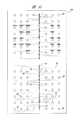
図1は、本実施形態の半導体装置の上面を示す平面図、図2は、この半導体装置の断面図、図3は、この半導体装置の下面を示す平面図である。
【0017】
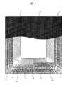
本実施形態の半導体装置は、パッケージ基板1の主面上に3個のチップ2A、2B、2Cを実装し、これらのチップ2A、2B、2Cをモールド樹脂3で封止したマルチチップモジュール(MCM)である。3個のチップ2A〜2Cのうち、2個のチップ2A、2Bは、パッケージ基板1の主面上に並べて配置され、それらの主面に形成された複数個のAuバンプ4を介してパッケージ基板1の配線5と電気的に接続されている。すなわち、チップ2A、2Bのそれぞれは、フリップチップ方式によって実装されている。
【0018】
チップ2A、2Bの主面(下面)とパッケージ基板1の主面との隙間には、アンダーフィル樹脂(封止樹脂)6が充填されている。チップ2Aは、例えばDRAMが形成されたシリコンチップであり、チップ2Bは、例えばフラッシュメモリが形成されたシリコンチップである。
【0019】
チップ2Cは、2個のチップ2A、2Bを跨ぐように配置され、接着剤7によってチップ2A、2Bの上面に接着されている。チップ2Cの主面に形成されたボンディングパッド13は複数本のAuワイヤ8によってパッケージ基板1のボンディングパッド9と電気的に接続されている。すなわち、チップ2Cは、ワイヤボンディング方式によって実装されている。チップ2Cは、例えば高速マイクロプロセッサ(MPU:超小型演算処理装置)が形成されたシリコンチップである。このチップ2Cの端子ピッチは、上記2個のチップ2A、2Bの端子ピッチよりも狭い。
【0020】
上記3個のチップ2A、2B、2Cを実装するパッケージ基板1は、ガラス繊維を含んだエポキシ樹脂(ガラス・エポキシ樹脂)のような汎用樹脂を主体として構成された多層配線基板であり、その主面(上面)、下面および内部に4〜6層程度の配線5が形成されている。
【0021】
パッケージ基板1の下面には、上記配線5と電気的に接続された複数の電極パッド10がアレイ状に配置されており、それぞれの電極パッド10には、マルチチップモジュール(MCM)の外部接続端子を構成する半田バンプ11が接続されている。マルチチップモジュール(MCM)は、これらの半田バンプ11を介して電子機器の配線基板などに実装される。パッケージ基板1の主面および下面には、配線5とチップ2A、2Bとの接続部、ボンディングパッド9、電極パッド10などの表面を除き、エポキシ系樹脂やアクリル系樹脂などからなるソルダレジスト12がコーティングされている。
【0022】
上記マルチチップモジュール(MCM)の寸法の一例を説明すると、パッケージ基板1の外形寸法は、縦×横=13mm×13mm、厚さ0.3mmである。パッケージ基板1に実装されたチップ2A、2B、2Cの厚さは、それぞれ0.15mm、並んで配置された2個のチップ2A、2Bの間隔は、20μm〜100μmである。チップ2A、2B、2Cを封止するモールド樹脂3の厚さは、0.66mm、モールド樹脂3の上面から半田バンプ11の下端までの距離、すなわちマルチチップモジュール(MCM)の実装高さは、1.468mmである。
【0023】
また、チップ2Aの主面に形成されたAuバンプ4のピッチは、0.08mm、チップ2Bの主面に形成されたAuバンプ4のピッチは、0.15mmである。一方、チップ2Cの主面に形成されたボンディングパッド13のピッチは、0.065mmである。すなわち、マイクロプロセッサが形成されたチップ2Cの端子ピッチは、DRAMが形成されたチップ2Aの端子ピッチおよびフラッシュメモリが形成されたチップ2Bの端子ピッチよりも狭い。
【0024】
このように、本実施形態のマルチチップモジュール(MCM)は、端子ピッチが比較的広いチップ2A、2Bをフリップチップ方式でパッケージ基板1に実装し、端子ピッチが最も狭いチップ2Cをチップ2A、2Bの上に積層してワイヤボンディング方式で実装する。
【0025】
これにより、配線5のピッチが広い安価な汎用樹脂基板にチップ2A、2B、2Cを実装することができるので、マルチチップモジュール(MCM)の製造コストを低減することができる。
【0026】
また、チップ2A、2Bの上にチップ2Cを積層することにより、パッケージ基板1の実装面積を小さくすることができるので、実装密度の高いマルチチップモジュール(MCM)を実現することができる。
【0027】
次に、上記のように構成された本実施形態の半導体装置の製造方法を図4〜図26を用いて工程順に説明する。
【0028】
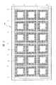
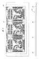
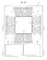
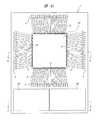
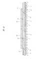
図4〜図8は、マルチチップモジュール(MCM)の製造に使用する長方形の基板(以下、マルチ配線基板100という)を示している。図4は、このマルチ配線基板100の主面(チップ実装面)を示す全体平面図、図5は、裏面を示す全体平面図である。また、図6は、マルチ配線基板100の一部を示す平面図と側面図、図7は、マルチ配線基板100の一部を示す断面図、図8は、マルチ配線基板100の一部(パッケージ基板1個分の領域)を示す拡大平面図である。
【0029】
マルチ配線基板100は、前記パッケージ基板1の母体となる基板である。このマルチ配線基板100を図4、図5に示すダイシングラインLに沿って格子状に切断(ダイシング)、個片化することにより、複数個のパッケージ基板1が得られる。図に示すマルチ配線基板100の場合は、その長辺方向が6ブロックのパッケージ基板形成領域に区画され、短辺方向が3ブロックのパッケージ基板形成領域に区画されているので、3×6=18個のパッケージ基板1が得られる。
【0030】
上記マルチ配線基板100は、ガラス・エポキシ樹脂のような汎用樹脂を主体として構成された多層配線基板である。マルチ配線基板100の主面には、配線5およびボンディングパッド9が形成されており、裏面には、電極パッド10が形成されている。また、マルチ配線基板100の内層には、複数層の配線5が形成されている。パッケージ基板1を、安価な汎用樹脂を使って製造することにより、マルチチップモジュール(MCM)の製造原価を低減することができる。
【0031】
マルチ配線基板100の主面の配線5およびボンディングパッド9と、裏面の電極パッド10は、マルチ配線基板100の両面に貼り付けたCu箔をエッチングすることによって形成される。マルチ配線基板100の主面の配線5のうち、ソルダレジスト12で覆われていない領域、すなわちチップ2A、2BのAuバンプ4が接続される領域の表面には、NiおよびAuのメッキが施されている。また、ボンディングパッド9の表面および電極パッド10の表面にも、NiおよびAuのメッキが施されている。これらのメッキは、無電解メッキ法で形成することもできるが、無電解メッキ法で形成したメッキ層は膜厚が薄く、ボンディングパッド9上にAuワイヤ4を接続したときに十分な接着強度が確保し難いので、上記NiおよびAuのメッキは、無電解メッキ法よりも膜厚を厚くすることのできる電解メッキ法で形成される。
【0032】
配線5、ボンディングパッド9および電極パッド10の表面に電解メッキ法でNiおよびAuのメッキを施す場合は、配線5、ボンディングパッド9および電極パッド10がマルチ配線基板100の全域で導通した状態でメッキ処理を行い、次いで、ダイシングラインL上の配線5をルータで切断した後、各パッケージ基板形成領域の導通試験を行う。そのため、図6および図7に示したように、マルチ配線基板100の主面のダイシングラインLには、この領域の配線5をルータで切断したときの溝101が残っている。
【0033】
図8に示すように、パッケージ基板形成領域の周辺部には、チップ実装領域を囲むように複数のボンディングパッド13が形成されている。ボンディングパッド13は、パッケージ基板形成領域の4辺に沿って2列に配置されている。ボンディングパッド13とチップ実装領域との間には、チップ実装領域を囲むようにダム領域16が設けられている。このダム領域16は、ソルダレジスト12が形成されていない領域であり、その内側および外側のソルダレジスト12が形成された領域よりも表面の高さが低くなっているため、チップ2A、2Bの下部にアンダーフィル樹脂6を充填する際、このアンダーフィル樹脂6がパッケージ基板形成領域の周辺部、すなわちボンディングパッド13が形成された領域に流れるのを防ぐ機能を持っている。
【0034】
上記マルチ配線基板100を使ってマルチチップモジュール(MCM)を製造するには、図9(パッケージ基板2個分の領域を示す断面図)および図10(パッケージ基板1個分の領域を示す拡大平面図)に示すように、マルチ配線基板100の主面のチップ実装領域に樹脂テープ6aを貼り付ける。樹脂テープ6aは、例えば粒径3μm程度のシリカを分散させた熱硬化型エポキシ系樹脂からなるもので、あらかじめ2個のチップ(チップ2A、2B)とほぼ同じ寸法となるように裁断しておく。樹脂テープ6aは、樹脂中に導電性の微粉末を分散させた異方性導電性樹脂(ACF)などで構成することもできる。
【0035】
なお、大気中に放置したマルチ配線基板100には大気中の水分が浸入しているため、そのまま樹脂テープ6aを貼り付けると、両者の接着性が低下する虞れがある。従って、マルチ配線基板100の主面に樹脂テープ6aを貼り付ける際には、その直前にマルチ配線基板100をベークして水分を除去しておくことが望ましい。ベーク条件は、例えば125℃、2時間程度である。また、上記ベーク処理に続いてマルチ配線基板100をプラズマ処理し、その表面を活性化することにより、樹脂テープ6aとマルチ配線基板100との接着性をさらに向上させることができる。
【0036】
次に、図11および図12に示すように、マルチ配線基板100の主面に貼り付けた樹脂テープ6aの上に2個のチップ2A、2Bをフェイスダウン方式で搭載する。このとき、チップ2Aとチップ2Bの隙間は、20μm〜100μm程度に設定する。
【0037】
図13に示すように、DRAMが形成されたチップ2Aの主面には、あらかじめボールボンディング法を用いてAuバンプ4を形成しておく。また、図14に示すように、フラッシュメモリが形成されたチップ2Bの主面にも、同様の方法でAuバンプ4を形成しておく。これらのAuバンプ4は、ウエハプロセスの最終工程で形成する。すなわち、通常のウエハプロセスが完了した後、ウエハのボンディングパッド上にボールボンディング法を用いてAuバンプ4を形成し、その後、ウエハをダイシングすることによって、個片化されたチップ2A、2Bを得る。
【0038】
通常、DRAMのボンディングパッドは、チップの中央に一列に配置されるが、フラッシュメモリのボンディングパッドは、チップの短辺に沿って2列に配置される。そのため、DRAMのボンディングパッドは、フラッシュメモリのそれに比べてパッドのピッチが狭くなり、それに伴ってパッドの径も小さくなる(例えばフラッシュメモリの端子ピッチが150μmの場合、DRAMのそれは85μm程度である)。従って、DRAMのボンディングパッド上にAuバンプ4を形成するときは、径の細い(例えば直径20μm)のAu線を使用し、フラッシュメモリのボンディングパッド上にAuバンプ4を形成するときは、径の太い(例えば直径30μm)のAu線を使用するのが通常である。
【0039】
しかし、本実施形態のマルチチップモジュール(MCM)は、2個のチップ2A、2Bの上に第3のチップ2Cを積層するので、チップの厚さおよびAuバンプ4の径を2個のチップ2A、2Bで同じにすることによって、両者の実装高さを揃える必要がある。従って、本実施形態では、フラッシュメモリのボンディングパッド上にAuバンプ4を形成するときに使用するAu線は、DRAMのボンディングパッド上にAuバンプ4を形成するときに使用するAu線と同じ径(例えば直径20μm)のものを使用する。この場合、ソルダレジスト12の厚さ(例えば25μm)を考慮すると、細いAu線を使って形成したAuバンプ4は、ボンディングパッドとの接触面積が少なくなる。そこで本実施形態では、Auバンプ4とボンディングパッドとの接触面積を確保するために、Auバンプ4の上にAuバンプ4を重ねてボンディングする多段バンプ構造を採用する。
【0040】
次に、図15に示すように、2個のチップ2A、2Bの上に底面が平坦なヒートツール102を押し当てる。ヒートツール102の加圧圧力は、例えば15kg/10mm2、温度は例えば235℃である。これにより、樹脂テープ6aが溶融し、チップ2A、2Bとマルチ配線基板100の隙間、およびチップ2Aとチップ2Bの隙間にアンダーフィル樹脂6が充填されると共に、チップ2A、2BのAuバンプ4とマルチ配線基板100の配線5(図15には示さない)とが電気的に接続される。
【0041】
このように、本実施形態では、チップ2A、2Bとほぼ同じ寸法に加工した樹脂テープ6aを溶融させることによって、チップ2A、2Bとマルチ配線基板100の隙間、およびチップ2Aとチップ2Bの隙間にアンダーフィル樹脂6を充填する。この方法によれば、例えばチップ2A、2Bの周辺にディスペンサを使って液状のアンダーフィル樹脂を供給する充填方法に比べた場合、アンダーフィル樹脂6がチップ2A、2Bの周囲にはみ出す量を少なくすることができるので、チップ2A、2Bを囲むように配置されたマルチ配線基板100上のボンディングパッド9がアンダーフィル樹脂6で覆われることはない。
【0042】
次に、図16および図17に示すように、2個のチップ2A、2Bの上にチップ2Cを搭載する。図18に示すように、マイクロプロセッサが形成されたチップ2Cの主面には、その4辺に沿ってボンディングパッド13が形成されている。ボンディングパッド13の数は、チップ2Aやチップ2Bに形成されたボンディングパッドの数よりも多い。
【0043】
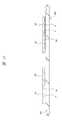
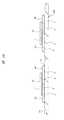
チップ2Cは、マルチ配線基板100とチップ2Cとを接続するAuワイヤ8の長さが出来るだけ均一になるよう、各パッケージ基板形成領域の中央に配置する。また、チップ2Cの裏面には、あらかじめチップ2Cと同じ寸法に裁断されたテープ状の接着剤7を貼り付けておく。チップ2Cの裏面にテープ状の接着剤7を貼り付けるには、例えば図19および図20に示すように、通常のウエハプロセスが完了したウエハ14の裏面にダイシングテープ15を貼り付ける際、ウエハ14とダイシングテープ15との間にテープ状の接着剤7を挟み込み、この状態でウエハ14をダイシングすることによってチップ2Cを得る。その後、チップ2Cの裏面のダイシングテープ15を除去すると、チップ2Cの裏面にチップ2Cと同寸法の接着剤7が残る。接着剤7は、例えばポリイミド樹脂系の接着剤を使用する。
【0044】
次に、マルチ配線基板100を加熱炉内で180℃、1時間程度加熱する。この加熱処理により、接着剤7が軟化し、チップ2A、2Bの上にチップ2Cが接着される。
【0045】
次に、図21および図22に示すように、マルチ配線基板100のボンディングパッド9とチップ2Cのボンディングパッド13(図21、22には示さない)とをAuワイヤ8で接続する。Auワイヤ8の接続は、例えば超音波振動と熱圧着とを併用したワイヤボンダを使用して行う。
【0046】
次に、図23および図24に示すように、マルチ配線基板100をモールド金型(図示せず)に装着し、マルチ配線基板100の主面全体を一括して樹脂封止する。モールド樹脂3は、例えば粒径70μm〜100μm程度のシリカを分散させた熱硬化型エポキシ系樹脂からなる。
【0047】
次に、図25に示すように、マルチ配線基板100の裏面の電極パッド9(図25には示さない)に半田バンプ11を接続する。半田バンプ11の接続は、例えば低融点のPb−Sn共晶合金からなる半田ボールを電極パッド9の表面に供給した後、半田ボールをリフローさせることによって行う。
【0048】
次に、図26に示すように、マルチ配線基板100を前記図4、図5に示すダイシングラインLに沿って切断、個片化することにより、前記図1〜図3に示した本実施形態のマルチチップモジュール(MCM)が完成する。
【0049】
(実施の形態2)
本実施形態の半導体装置の製造方法を図27〜図37を用いて工程順に説明する。
【0050】
前記実施の形態1では、DRAMが形成されたチップ2Aの主面およびフラッシュメモリが形成されたチップ2Bの主面にそれぞれAuバンプ4を形成したが、本実施形態では、Auバンプ4に代えて半田バンプ20を使用する。また、DRAMが形成されたチップ2Aとフラッシュメモリが形成されたチップ2Bの組み合わせに代えて、DRAMが形成されたチップ2Aを2個使用する。
【0051】
また、本実施形態では、マルチ配線基板100の主面に実装する2種類のチップ2A、2Cのそれぞれの端子数に対するチップ面積の比(この比をグリッドアレイ指数と称する)を比較し、このグリッドアレイ指数が小さい方のチップは、ワイヤボンディング方式で実装し、グリッドアレイ指数が大きい方のチップは、フリップチップ方式で実装する。すなわち、第1チップの端子数、第2チップの端子数をそれぞれN1、N2とし、第1チップの主面の面積、第2チップの主面の面積をそれぞれS1、S2とした場合に、SQRT(S1/N1)>SQRT(S2/N2)(SQRTは平方根を表す)の関係が成立した場合は、第1チップをフリップチップ方式で実装し、第2チップをワイヤボンディング方式で実装する。ここで、チップの端子数とは、チップの主面に半田バンプをアレイ状に配置したときの半田バンプピッチである。同様に、端子数あるいは面積が異なる3種類以上のチップを実装する場合には、それらのチップのグリッドアレイ指数を算出し、グリッドアレイ指数が最も小さいチップをワイヤボンディング方式で実装し、その他のチップは、フリップチップ方式で実装する。
【0052】
DRAMが形成されたチップ2Aのサイズは、一例として4.66mm×8.22mm、チップ2Aの中央に一列に配置された端子(ボンディングパッド)の数は64ピン、端子のピッチは0.08mmである。一方、マイクロプロセッサが形成されたチップ2Cのサイズは、一例として6.84mm×6.84mm、チップ2Cの4辺に配置された端子数は256ピン、端子のピッチは0.065mmである。この場合、2種類のチップ2A、2Cのグリッドアレイ指数を計算すると、マイクロプロセッサが形成されたチップ2Cの方が小さい。従って、本実施形態では、チップ2Cをワイヤボンディング方式で実装し、チップ2Aをフリップチップ方式で実装する。
【0053】
図27は、DRAMが形成されたチップ2Aの主面に半田バンプ20を形成した状態を示す平面図である。図示のように、半田バンプ20は、チップ2Aの主面にアレイ状に配置されている。ボンディングパッド13と半田バンプ20とは、Cu配線21を介して電気的に接続されている。Cu配線21は、ボンディングパッド13のピッチを半田バンプ20のピッチに変換するインターポーザとして機能し、これによって半田バンプ20のピッチをボンディングパッド13のピッチよりも広くすることができる。
【0054】
上記Cu配線21および半田バンプ20は、ウエハレベルCSP技術を利用し、ウエハプロセスの最終工程で形成される。すなわち、図28に示すように、Cu配線21は、ウエハ14の表面保護膜22上にポリイミド樹脂などの有機絶縁膜23を形成した後、この有機絶縁膜23上に電解メッキ法などを用いて形成される。Cu配線21とボンディングパッド13は、ボンディングパッド13上の有機絶縁膜23に形成したスルーホール24を通じて電気的に接続される。また、半田バンプ20は、Cu配線21の一端である電極パッド21aの表面にスクリーン印刷法で半田ペーストを印刷し、次に、ウエハ14を加熱してこの半田ペーストを溶融させることによって形成される。半田バンプ20は、例えば2重量%のSnを含むPb−Sn合金(液相線温度320℃〜325℃)などで構成される。
【0055】
次に、図29に示すように、マルチ配線基板100のそれぞれのパッケージ基板形成領域に2個のチップ2A、2Aをフェイスダウン方式で位置決めした後、マルチ配線基板100を加熱して半田バンプ20をリフローすることにより、チップ2A、2Aの半田バンプ20とマルチ配線基板100の配線5とを電気的に接続する。
【0056】
次に、図30に示すように、2個のチップ2A、2Aの上にチップ2Cを搭載する。チップ2A、2Aとチップ2Cとの接着は、前記実施の形態1と同様、チップ2Cの裏面に貼り付けた接着剤7を使用する。
【0057】
図31は、チップ2Aの端子配列を示す平面図、図32は、チップ2Cの端子配列を示す平面図である。図示のように、チップ2AのDQピンは、チップの主面の特定の箇所に集中して配置されており、チップ2CのDQピンも同様である。そこで、チップ2A、2Aの上にチップ2Cを搭載するときは、チップ2A、2Aとチップ2Cの共通するDQピンが最も近接するような位置にチップ2A、2A、2Cを配置するとよい。このようにすると、図33に示すように、DQピン同士を接続するAuワイヤ8の長さをほぼ等しくすることができるので、Auワイヤ8の引き回し効率が向上する。図34は、DRAMが形成された4個のチップ2Aの上にマイクロプロセッサが形成された1個のチップ2Cを搭載する時の最適な配置の例を示している。
【0058】
次に、図35に示すように、チップ2A、2Aの周辺部にディスペンサなどを使って液状のアンダーフィル樹脂6を供給した後、アンダーフィル樹脂6を加熱、硬化させることによって、チップ2A、2Aとマルチ配線基板100の隙間、およびチップ2Aとチップ2Bの隙間にアンダーフィル樹脂6を充填する。
【0059】
次に、図36に示すように、マルチ配線基板100をモールド金型(図示せず)に装着し、マルチ配線基板100の主面全体を一括して樹脂封止した後、図37に示すように、マルチ配線基板100の裏面の電極パッド9に半田バンプ11を接続する。図示は省略するが、その後、前記実施の形態1と同様の方法でマルチ配線基板100を切断することにより、本実施形態のマルチチップモジュール(MCM)が完成する。
【0060】
以上、本発明者によってなされた発明を前記実施の形態に基づき具体的に説明したが、本発明は前記実施の形態に限定されるものではなく、その要旨を逸脱しない範囲で種々変更可能であることはいうまでもない。
【0061】
前記実施の形態では、ワイヤボンディング方式で実装するチップ2Cをフリップチップ方式で実装するチップ2A(または2B)の上に配置したが、パッケージ基板1の実装面積が大きくなっても差し支えないような場合は、図38〜図40あるいは図41〜図43に示すように、ワイヤボンディング方式で実装するチップ2Cをフリップチップ方式で実装するチップ2A(または2B)の横に配置してもよい。図38〜図40に示す例は、実施の形態1で用いたチップ2A、2B、2Cを組み合わせた例であり、図41〜図43に示す例は、実施の形態2で用いたチップ2A、2Cを組み合わせた例である。
【0062】
また、図44〜図50に示すように、複数個のチップをパッケージ基板に実装する手段に代えて、パッケージ基板を実装するマザーボード200に直接実装してもよい。図44、図45に示す例は、フリップフロップ方式で実装するチップ2Aの端子をAuバンプ4で構成した例である。また、図46、図47に示す例は、フリップフロップ方式で実装するチップ2Aの端子を半田バンプ20で構成し、チップの主面にアレイ状に配置した例である。また、図48〜図50に示す例は、ワイヤボンディング方式で実装するチップ2Cをフリップチップ方式で実装するチップ2Aの横に配置した例である。
【0063】
パッケージ基板上には、コンデンサや抵抗素子など、チップ以外の小型電子部品を実装することもできる。例えば、メモリチップの外周に沿ってチップコンデンサを搭載することにより、メモリチップの駆動時に生じるノイズを低減して高速動作を実現することができる。
【0064】
本発明は、チップを実装するパッケージ基板としてビルドアップ基板の使用を排除するものではない。ビルドアップ基板の使用する場合でも、本発明を適用することにより、配線ピッチのより広いビルドアップ基板を使用することができるので、配線ピッチの狭い高価なビルドアップ基板を使用する場合に比べてマルチチップモジュールの製造コストを低減することができる。
【0065】
【発明の効果】
本願によって開示される発明のうち、代表的なものによって得られる効果を簡単に説明すれば、以下の通りである。
【0066】
本発明の好ましい一実施態様によれば、複数個のチップの上に他のチップを積層して樹脂封止したマルチチップモジュールの製造コストを低減することができる。
【図面の簡単な説明】
【図1】本発明の一実施形態である半導体装置の平面図である。
【図2】本発明の一実施形態である半導体装置の断面図である。
【図3】本発明の一実施形態である半導体装置の平面図である。
【図4】本発明の一実施形態である半導体装置の製造に用いるマルチ配線基板の平面図である。
【図5】本発明の一実施形態である半導体装置の製造に用いるマルチ配線基板の平面図である。
【図6】図5に示すマルチ配線基板の要部拡大平面図である。
【図7】図5に示すマルチ配線基板の要部拡大断面図である。
【図8】図5に示すマルチ配線基板の要部拡大平面図である。
【図9】本発明の一実施形態である半導体装置の製造方法を示すマルチ配線基板の要部拡大断面図である。
【図10】本発明の一実施形態である半導体装置の製造方法を示すマルチ配線基板の要部拡大平面図である。
【図11】本発明の一実施形態である半導体装置の製造方法を示すマルチ配線基板の要部拡大断面図である。
【図12】本発明の一実施形態である半導体装置の製造方法を示すマルチ配線基板の要部拡大平面図である。
【図13】本発明の一実施形態である半導体装置の製造に用いる半導体チップの平面図である。
【図14】本発明の一実施形態である半導体装置の製造に用いる半導体チップの平面図である。
【図15】本発明の一実施形態である半導体装置の製造方法を示すマルチ配線基板の要部拡大断面図である。
【図16】本発明の一実施形態である半導体装置の製造方法を示すマルチ配線基板の要部拡大断面図である。
【図17】本発明の一実施形態である半導体装置の製造方法を示すマルチ配線基板の要部拡大平面図である。
【図18】本発明の一実施形態である半導体装置の製造に用いる半導体チップの平面図である。
【図19】本発明の一実施形態である半導体装置の製造方法を示す半導体ウエハの斜視図である。
【図20】本発明の一実施形態である半導体装置の製造方法を示す半導体ウエハの側面図である。
【図21】本発明の一実施形態である半導体装置の製造方法を示すマルチ配線基板の要部拡大断面図である。
【図22】本発明の一実施形態である半導体装置の製造方法を示すマルチ配線基板の要部拡大平面図である。
【図23】本発明の一実施形態である半導体装置の製造方法を示すマルチ配線基板の平面図である。
【図24】本発明の一実施形態である半導体装置の製造方法を示すマルチ配線基板の要部拡大断面図である。
【図25】本発明の一実施形態である半導体装置の製造方法を示すマルチ配線基板の要部拡大断面図である。
【図26】本発明の一実施形態である半導体装置の製造方法を示すマルチ配線基板の要部拡大断面図である。
【図27】本発明の他の実施形態である半導体装置の製造に用いる半導体チップの平面図である。
【図28】本発明の他の実施形態である半導体装置の製造方法を示す半導体ウエハの要部拡大断面図である。
【図29】本発明の他の実施形態である半導体装置の製造方法を示すマルチ配線基板の要部拡大断面図である。
【図30】本発明の他の実施形態である半導体装置の製造方法を示すマルチ配線基板の要部拡大断面図である。
【図31】DRAMが形成された半導体チップの端子配列を示す平面図である。
【図32】マイクロプロセッサが形成された半導体チップの端子配列を示す平面図である。
【図33】本発明の一実施形態である半導体装置の製造方法を示すマルチ配線基板の要部拡大平面図である。
【図34】本発明の他の実施形態である半導体装置の製造方法を示すマルチ配線基板の要部拡大平面図である。
【図35】本発明の他の実施形態である半導体装置の製造方法を示すマルチ配線基板の要部拡大断面図である。
【図36】本発明の他の実施形態である半導体装置の製造方法を示すマルチ配線基板の要部拡大断面図である。
【図37】本発明の他の実施形態である半導体装置の製造方法を示すマルチ配線基板の要部拡大断面図である。
【図38】本発明の他の実施形態である半導体装置を示す平面図である。
【図39】図38のA−A’線に沿った断面図である。
【図40】図38のB−B’線に沿った断面図である。
【図41】本発明の他の実施形態である半導体装置を示す平面図である。
【図42】図41のA−A’線に沿った断面図である。
【図43】図41のB−B’線に沿った断面図である。
【図44】本発明の他の実施形態である半導体装置を示す平面図である。
【図45】図44のA−A’線に沿った断面図である。
【図46】本発明の他の実施形態である半導体装置を示す平面図である。
【図47】図46のA−A’線に沿った断面図である。
【図48】本発明の他の実施形態である半導体装置を示す平面図である。
【図49】図48のA−A’線に沿った断面図である。
【図50】図48のB−B’線に沿った断面図である。
【符号の説明】
1 パッケージ基板
2 半導体ウエハ
2A、2B、2C 半導体チップ
3 モールド樹脂(第2封止樹脂)
4 Auバンプ
5 配線
6 アンダーフィル樹脂(第1封止樹脂)
6a 樹脂テープ
7 接着剤
8 Auワイヤ
9 ボンディングパッド
10 電極パッド
11 半田バンプ
12 ソルダレジスト
13 ボンディングパッド
14 ウエハ
15 ダイシングテープ
20 半田バンプ
21 Cu配線
21a 電極パッド
22 表面保護膜
23 有機絶縁膜
24 スルーホール
100 マルチ配線基板
101 溝
102 ヒートツール
200 マザーボード
L ダイシングライン[0001]
BACKGROUND OF THE INVENTION
The present invention relates to a semiconductor device and a manufacturing technique thereof, and more particularly to a technique effective when applied to a multi-chip module (MCM) in which a plurality of types of semiconductor chips having different terminal pitches are mounted on a wiring board.
[0002]
[Prior art]
As a measure to increase the capacity of memory LSIs such as flash memory and DRAM (Dynamic Random Access Memory), semiconductor chips (memory chips) on which these memory LSIs are formed are stacked and sealed in a single package Various memory module structures have been proposed.
[0003]
For example, Japanese Patent Laid-Open No. 4-302164 discloses a bonding pad in which a plurality of semiconductor chips having the same function and the same size are stacked stepwise through an insulating layer in one package, and exposed to the stepped portion of each semiconductor chip. And a package structure in which an inner lead of the package is electrically connected via a wire.
[0004]
In Japanese Patent Laid-Open No. 11-204720, a first semiconductor chip is mounted on an insulating substrate via a thermocompression-bonding sheet, and the outer dimension is the first through the thermocompression-bonding sheet on the first semiconductor chip. A second semiconductor chip smaller than the semiconductor chip is mounted, the bonding pads of the first and second semiconductor chips and the wiring layer on the insulating substrate are electrically connected via wires, and the first and second A package structure in which a semiconductor chip and a wire are sealed with a resin is disclosed.
[0005]
In addition, solder bumps are arranged in an array on the main surface of the semiconductor chip, and the bonding pads and the solder bumps are electrically connected via wiring made of Cu (copper) or the like, so that the connection terminals (solder bumps) A technique called a wafer level CSP (Chip Size Package) or a wafer process package (WPP) that makes the pitch wider than the pitch of bonding pads is known. If this technology is used, the terminal pitch of the semiconductor chip can be substantially widened, so that an inexpensive resin with a wide wiring pitch can be used without using an expensive build-up board with a narrow line and space of wiring. A memory module can be manufactured using the substrate. As for the wafer level CSP, for example, “Electronic packaging technology: 2000 extra edition” published by Technical Research Committee, Inc. (issued on May 28, 2000), pages 81 to 113, and International Patent Publication WO / 23696. There is a description.
[0006]
[Problems to be solved by the invention]
The present inventors have developed a multi-chip module in which a plurality of semiconductor chips (hereinafter simply referred to as chips) are mounted in one package.
[0007]
The multi-chip module under development by the present inventors was formed with a chip on which a memory LSI such as DRAM (Dynamic Random Access Memory) or flash memory was formed, and a high-speed microprocessor (MPU: ultra-compact processing unit). By sealing the chips in a single resin package, a system with higher versatility than a conventional memory module in which a plurality of memory chips are sealed with resin is to be realized.
[0008]
In addition, the present inventors are considering mounting a chip on an inexpensive resin substrate having a wide wiring pitch in order to reduce the manufacturing cost of the multichip module. For this purpose, it is necessary to substantially widen the terminal pitch of the chip by using the wafer level CSP technology described above.
[0009]
However, there is no problem in the case of a chip having a relatively small number of terminals, such as a chip in which a memory LSI such as a DRAM or a flash memory is formed, but a chip having a large number of terminals, such as a chip in which a microprocessor is formed. In this case, even if the wafer level CSP technology is used, there is a limit to substantially widen the terminal pitch of the chip.
[0010]
For example, the minimum pitch of wiring that can be formed on an inexpensive resin substrate using the current wiring board manufacturing technology is 0.5 mm. On the other hand, for example, when forming a solder bump with a pitch of 0.5 mm using a wafer process / package technology on a DRAM having a chip size of 4.66 mm × 8.22 mm, 64 pins, and a terminal pitch of 0.08 mm. There is no problem because a solder bump of 128 pins at the maximum can be formed. However, for example, if solder bumps with a pitch of 0.5 mm are formed on a microprocessor with a chip size of 6.84 mm × 6.84 mm, 256 pins, and a terminal pitch of 0.08 mm, a solder bump with a maximum of 169 pins will be formed. Since this chip can only be formed, an expensive build-up substrate having a wiring pitch of 0.4 mm or less is required when this chip is to be mounted by the flip chip method.
[0011]
An object of the present invention is to provide a technique capable of reducing the manufacturing cost of a multichip module in which a plurality of types of chips having different terminal pitches are mounted on a wiring board.
[0012]
The above and other objects and novel features of the present invention will be apparent from the description of this specification and the accompanying drawings.
[0013]
[Means for Solving the Problems]
Of the inventions disclosed in the present application, the outline of typical ones will be briefly described as follows.
[0014]
The semiconductor device of the present invention isSurface, formed on the surfaceMultiple wiring,Formed on the surface; andElectrically connected to the plurality of wirings;And,A plurality of arranged at the first pitchFirstBonding padAnd a plurality of second bonding pads which are arranged on the peripheral edge side of the surface with respect to the plurality of first bonding pads on the surface and arranged at a second pitch.A wiring board having a first integrated circuit,AndAnd the plurality of wiring boards.FirstSame as bonding padTimeA first main surface on which a plurality of first terminals arranged at a pitch is formed, and the first main surface is mounted on the surface of the wiring board so as to face the surface of the wiring board. The first semiconductor chip, the plurality of first terminals of the first semiconductor chip, and the front of the wiring board.WritingA plurality of bump electrodes for electrically connecting a number of first bonding pads, a second integrated circuit,AndAnd a second main surface on which a plurality of second terminals are formed, and a second back surface opposite to the second main surface is a first surface opposite to the first main surface of the first semiconductor chip. The second semiconductor chip stacked on the first semiconductor chip so as to face the back surface, the plurality of second terminals of the second semiconductor chip, and the front of the wiring boardWritingA plurality of wires, each electrically connecting a number of second bonding pads,The plurality of first terminals are arranged along a first side of the first main surface of the first semiconductor chip in a plan view, and the plurality of second terminals are the second terminals in a plan view. Arranged along the second side of the second main surface of the semiconductor chip,The plurality of second terminals of the second semiconductor chipAmong the plurality of first terminals of the first semiconductor chip, the pitch between the second terminals adjacent to each other along the first side is the pitch between the second terminals adjacent to each other along the second side. ofNarrower than the pitchYes.
[0015]
DETAILED DESCRIPTION OF THE INVENTION
Hereinafter, embodiments of the present invention will be described in detail with reference to the drawings. In all the drawings for explaining the embodiments, the same reference numerals are given to the same members, and the repeated explanation thereof is omitted.
[0016]
(Embodiment 1)
1 is a plan view showing the upper surface of the semiconductor device of the present embodiment, FIG. 2 is a cross-sectional view of the semiconductor device, and FIG. 3 is a plan view showing the lower surface of the semiconductor device.
[0017]
In the semiconductor device of this embodiment, three
[0018]
An underfill resin (sealing resin) 6 is filled in a gap between the main surfaces (lower surfaces) of the
[0019]
The
[0020]
The
[0021]
A plurality of
[0022]
An example of the dimensions of the multichip module (MCM) will be described. The external dimensions of the
[0023]
The pitch of the Au bumps 4 formed on the main surface of the
[0024]
Thus, in the multichip module (MCM) of this embodiment, the
[0025]
As a result, the
[0026]
In addition, since the mounting area of the
[0027]
Next, a method for manufacturing the semiconductor device of the present embodiment configured as described above will be described in the order of steps with reference to FIGS.
[0028]
4 to 8 show a rectangular substrate (hereinafter referred to as a multi-wiring substrate 100) used for manufacturing a multi-chip module (MCM). 4 is an overall plan view showing the main surface (chip mounting surface) of the
[0029]
The
[0030]
The
[0031]
The
[0032]
When the surfaces of the
[0033]
As shown in FIG. 8, a plurality of
[0034]
In order to manufacture a multi-chip module (MCM) using the
[0035]
In addition, since the moisture in the atmosphere has entered the
[0036]
Next, as shown in FIGS. 11 and 12, the two
[0037]
As shown in FIG. 13, Au bumps 4 are formed in advance on the main surface of the
[0038]
Usually, DRAM bonding pads are arranged in a row at the center of the chip, whereas flash memory bonding pads are arranged in two rows along the short side of the chip. Therefore, the bonding pad of the DRAM has a smaller pad pitch than that of the flash memory, and accordingly, the pad diameter also decreases (for example, when the terminal pitch of the flash memory is 150 μm, that of the DRAM is about 85 μm). . Therefore, when forming the
[0039]
However, since the multichip module (MCM) of this embodiment laminates the
[0040]
Next, as shown in FIG. 15, a
[0041]
As described above, in this embodiment, the resin tape 6a processed to have substantially the same dimensions as the
[0042]
Next, as shown in FIGS. 16 and 17, the
[0043]
The
[0044]
Next, the
[0045]
Next, as shown in FIGS. 21 and 22, the
[0046]
Next, as shown in FIGS. 23 and 24, the
[0047]
Next, as shown in FIG. 25, solder bumps 11 are connected to the electrode pads 9 (not shown in FIG. 25) on the back surface of the
[0048]
Next, as shown in FIG. 26, the
[0049]
(Embodiment 2)
A manufacturing method of the semiconductor device of this embodiment will be described in the order of steps with reference to FIGS.
[0050]
In the first embodiment, the Au bumps 4 are formed on the main surface of the
[0051]
In the present embodiment, the ratio of the chip area to the number of terminals of each of the two types of
[0052]
The size of the
[0053]
FIG. 27 is a plan view showing a state in which solder bumps 20 are formed on the main surface of the
[0054]
The
[0055]
Next, as shown in FIG. 29, after positioning the two
[0056]
Next, as shown in FIG. 30, the
[0057]
FIG. 31 is a plan view showing the terminal arrangement of the
[0058]
Next, as shown in FIG. 35, after supplying the
[0059]
Next, as shown in FIG. 36, the
[0060]
The invention made by the present inventor has been specifically described based on the above embodiment, but the present invention is not limited to the above embodiment, and various modifications can be made without departing from the scope of the invention. Needless to say.
[0061]
In the above embodiment, the
[0062]
As shown in FIGS. 44 to 50, instead of means for mounting a plurality of chips on a package substrate, they may be directly mounted on a
[0063]
Small electronic components other than chips, such as capacitors and resistor elements, can also be mounted on the package substrate. For example, by mounting a chip capacitor along the outer periphery of the memory chip, noise generated when the memory chip is driven can be reduced and high-speed operation can be realized.
[0064]
The present invention does not exclude the use of a build-up substrate as a package substrate for mounting a chip. Even when a build-up board is used, by applying the present invention, a build-up board with a wider wiring pitch can be used. The manufacturing cost of the chip module can be reduced.
[0065]
【The invention's effect】
The effects obtained by the representative ones of the inventions disclosed by the present application will be briefly described as follows.
[0066]
According to a preferred embodiment of the present invention, it is possible to reduce the manufacturing cost of a multi-chip module in which other chips are stacked on a plurality of chips and sealed with resin.
[Brief description of the drawings]
FIG. 1 is a plan view of a semiconductor device according to an embodiment of the present invention.
FIG. 2 is a cross-sectional view of a semiconductor device according to an embodiment of the present invention.
FIG. 3 is a plan view of a semiconductor device according to an embodiment of the present invention.
FIG. 4 is a plan view of a multi-wiring substrate used for manufacturing a semiconductor device according to an embodiment of the present invention.
FIG. 5 is a plan view of a multi-wiring substrate used for manufacturing a semiconductor device according to an embodiment of the present invention.
6 is an enlarged plan view of a main part of the multi-wiring substrate shown in FIG.
7 is an enlarged cross-sectional view of a main part of the multi-wiring substrate shown in FIG.
FIG. 8 is an enlarged plan view of a main part of the multi-wiring substrate shown in FIG.
FIG. 9 is an enlarged cross-sectional view of a main part of a multi-wiring substrate showing a method for manufacturing a semiconductor device according to an embodiment of the present invention.
FIG. 10 is an enlarged plan view of a main part of a multi-wiring substrate showing a method for manufacturing a semiconductor device according to an embodiment of the present invention.
FIG. 11 is an enlarged cross-sectional view of a main part of a multi-wiring substrate showing a method for manufacturing a semiconductor device according to an embodiment of the present invention.
FIG. 12 is an enlarged plan view of a main part of a multi-wiring substrate showing a method for manufacturing a semiconductor device according to an embodiment of the present invention.
FIG. 13 is a plan view of a semiconductor chip used for manufacturing a semiconductor device according to an embodiment of the present invention;
FIG. 14 is a plan view of a semiconductor chip used for manufacturing a semiconductor device according to an embodiment of the present invention;
FIG. 15 is an enlarged cross-sectional view of a main part of a multi-wiring substrate showing a method for manufacturing a semiconductor device according to an embodiment of the present invention.
FIG. 16 is an enlarged cross-sectional view of a main part of a multi-wiring substrate showing a method for manufacturing a semiconductor device according to an embodiment of the present invention.
FIG. 17 is an enlarged plan view of a main part of a multi-wiring substrate showing a method for manufacturing a semiconductor device according to an embodiment of the present invention.
FIG. 18 is a plan view of a semiconductor chip used for manufacturing a semiconductor device according to an embodiment of the present invention;
FIG. 19 is a perspective view of a semiconductor wafer showing a method for manufacturing a semiconductor device according to an embodiment of the present invention.
20 is a side view of a semiconductor wafer showing a method for manufacturing a semiconductor device according to an embodiment of the present invention; FIG.
21 is an essential part enlarged cross-sectional view of a multi-wiring board showing a method of manufacturing a semiconductor device according to an embodiment of the present invention; FIG.
FIG. 22 is an essential part enlarged plan view of the multi-wiring board showing the method of manufacturing a semiconductor device according to one embodiment of the present invention;
FIG. 23 is a plan view of a multi-wiring substrate showing a method of manufacturing a semiconductor device according to an embodiment of the present invention.
24 is an essential part enlarged cross-sectional view of a multi-wiring board showing a method of manufacturing a semiconductor device according to an embodiment of the present invention; FIG.
FIG. 25 is an enlarged cross-sectional view of a relevant part of a multi-wiring substrate showing a method for manufacturing a semiconductor device according to an embodiment of the present invention;
FIG. 26 is an essential part enlarged cross-sectional view of a multi-wiring board showing a method of manufacturing a semiconductor device according to an embodiment of the present invention;
FIG. 27 is a plan view of a semiconductor chip used for manufacturing a semiconductor device according to another embodiment of the present invention;
FIG. 28 is an enlarged cross-sectional view of a relevant part of a semiconductor wafer showing a method of manufacturing a semiconductor device according to another embodiment of the present invention.
FIG. 29 is an essential part enlarged cross-sectional view of a multi-wiring board showing a method of manufacturing a semiconductor device according to another embodiment of the present invention;
30 is an enlarged cross-sectional view of a relevant part of a multi-wiring substrate showing a method of manufacturing a semiconductor device according to another embodiment of the present invention. FIG.
FIG. 31 is a plan view showing a terminal arrangement of a semiconductor chip on which a DRAM is formed;
FIG. 32 is a plan view showing a terminal arrangement of a semiconductor chip on which a microprocessor is formed.
FIG. 33 is an enlarged plan view of the main part of the multi-wiring substrate showing the method of manufacturing a semiconductor device according to one embodiment of the present invention.
FIG. 34 is an enlarged plan view of an essential part of a multi-wiring board showing a method of manufacturing a semiconductor device according to another embodiment of the present invention.
FIG. 35 is an enlarged cross-sectional view of a relevant part of a multi-wiring substrate showing a method of manufacturing a semiconductor device according to another embodiment of the present invention.
FIG. 36 is an enlarged cross-sectional view of a relevant part of a multi-wiring substrate showing a method of manufacturing a semiconductor device according to another embodiment of the present invention.
FIG. 37 is an essential part enlarged cross-sectional view of a multi-wiring board showing a method of manufacturing a semiconductor device in another embodiment of the present invention;
FIG. 38 is a plan view showing a semiconductor device according to another embodiment of the present invention.
FIG. 39 is a cross-sectional view taken along line A-A ′ of FIG. 38.
40 is a cross-sectional view taken along line B-B ′ of FIG. 38. FIG.
FIG. 41 is a plan view showing a semiconductor device according to another embodiment of the present invention.
42 is a cross-sectional view taken along line A-A ′ of FIG. 41. FIG.
43 is a cross-sectional view taken along line B-B ′ of FIG. 41. FIG.
FIG. 44 is a plan view showing a semiconductor device according to another embodiment of the present invention.
45 is a cross-sectional view taken along line A-A ′ of FIG. 44. FIG.
FIG. 46 is a plan view showing a semiconductor device according to another embodiment of the present invention.
47 is a cross-sectional view taken along line A-A ′ of FIG. 46. FIG.
FIG. 48 is a plan view showing a semiconductor device according to another embodiment of the present invention.
49 is a cross-sectional view taken along line A-A ′ of FIG. 48. FIG.
50 is a cross-sectional view taken along line B-B ′ of FIG. 48. FIG.
[Explanation of symbols]
1 Package substrate
2 Semiconductor wafer
2A, 2B, 2C Semiconductor chip
3 Mold resin (second sealing resin)
4 Au bump
5 Wiring
6 Underfill resin (first sealing resin)
6a Resin tape
7 Adhesive
8 Au wire
9 Bonding pads
10 Electrode pad
11 Solder bump
12 Solder resist
13 Bonding pads
14 Wafer
15 Dicing tape
20 Solder bump
21 Cu wiring
21a Electrode pad
22 Surface protective film
23 Organic insulation film
24 through hole
100 Multi-wiring board
101 groove
102 Heat tool
200 Motherboard
L Dicing line
Claims (11)
Translated fromJapanese第1集積回路、および前記配線基板の前記複数の第1ボンディングパッドと同じピッチで配置された複数の第1端子が形成された第1主面を有し、前記第1主面が前記配線基板の前記表面と対向するように、前記配線基板の前記表面上に搭載された第1半導体チップと、
前記第1半導体チップの前記複数の第1端子と、前記配線基板の前記複数の第1ボンディングパッドとを、それぞれ電気的に接続する複数のバンプ電極と、
第2集積回路、および複数の第2端子が形成された第2主面を有し、前記第2主面とは反対側の第2裏面が前記第1半導体チップの前記第1主面とは反対側の第1裏面と対向するように、前記第1半導体チップ上に積層された第2半導体チップと、
前記第2半導体チップの前記複数の第2端子と、前記配線基板の前記複数の第2ボンディングパッドとを、それぞれ電気的に接続する複数のワイヤと、
を含み、
前記複数の第1端子は、平面視において、前記第1半導体チップの前記第1主面における第1辺に沿って配置されており、
前記複数の第2端子は、平面視において、前記第2半導体チップの前記第2主面における第2辺に沿って配置されており、
前記第2半導体チップの前記複数の第2端子のうち、前記第2辺に沿って互いに隣り合う第2端子間のピッチは、前記第1半導体チップの前記複数の第1端子のうち、前記第1辺に沿って互いに隣り合う第1端子間のピッチよりも狭いことを特徴とする半導体装置。Surface, a plurality of wiresformed on the surface,is formed on the surface, and wherein a plurality of wirings electrically connected,and a plurality offirst bonding pads disposed at a firstpitch, and the surface A wiring board havinga plurality of second bonding pads arranged at a second pitch and arranged on the peripheral edge side of the surface from the plurality of first bonding pads ;
The first integrated circuit,and having a first major surface, wherein the plurality offirst bonding pads and a plurality of first terminals disposed at thesame pitch is formed of the wiring substrate, said first major surface A first semiconductor chip mounted on the surface of the wiring board so as to face the surface of the wiring board;
And wherein the plurality of first terminals of the first semiconductor chip, a first bonding pad of the priorKifuku number of the wiring substrate, a plurality of bump electrodes electrically connected,
The second integrated circuit,and a plurality of second major surface the second terminal is formed, the first major surface of said second back surface opposite to the second main surface of the first semiconductor chip A second semiconductor chip stacked on the first semiconductor chip so as to face the first back surface opposite to the first semiconductor chip;
Said second semiconductor chip of the plurality of second terminals of the second bonding pads of the frontKifuku number of the wiring substrate, a plurality of wires electrically connected,
Including
The plurality of first terminals are arranged along a first side of the first main surface of the first semiconductor chip in plan view,
The plurality of second terminals are arranged along a second side of the second main surface of the second semiconductor chip in plan view,
Among the plurality of second terminalsof the second semiconductor chip,the pitch between the second terminals adjacent to each other along the second side is the first of the plurality of first terminals of the first semiconductor chip. wherein a andgo narrower than the pitchbetween the first terminal adjacent to each other along one side.
前記複数の半田バンプは、前記配線基板の前記複数の第1および第2ボンディングパッドとそれぞれ電気的に接続されていることを特徴とする請求項1記載の半導体装置。A plurality of solder bumps are arranged on the back surface opposite to the front surface of the wiring board,
2. The semiconductor device according to claim 1, wherein the plurality of solder bumps are electrically connected to the plurality offirst and second bonding pads ofthe wiring board, respectively.
前記銅配線は、電解めっき法により形成されていることを特徴とする請求項1記載の半導体装置。Wherein the first semiconductor chip has a first major surface to form surface protective film, the surface protective film on the formed organic insulating layer, copper wiring formed onand the organic insulating layer ,
The semiconductor device according to claim 1, wherein the copper wiring is formed by an electrolytic plating method.
前記バンプ電極は、前記銅配線の前記第1端部上に配置されていることを特徴とする請求項10記載の半導体装置。The first terminal of the first semiconductor chip corresponds to a first end of the copper wiring;
The semiconductor device according to claim 10, wherein the bump electrode is disposed on the first end of the copper wiring.
Priority Applications (5)
| Application Number | Priority Date | Filing Date | Title |
|---|---|---|---|
| JP2001173134AJP4790157B2 (en) | 2001-06-07 | 2001-06-07 | Semiconductor device |
| US10/132,239US6841881B2 (en) | 2001-06-07 | 2002-04-26 | Semiconductor device and a method of manufacturing the same |
| TW91109006ATW558818B (en) | 2001-06-07 | 2002-04-30 | Semiconductor device and its manufacturing method |
| KR20020025228AKR100856609B1 (en) | 2001-06-07 | 2002-05-08 | A semiconductor device and a method of manufacturing the same |
| US10/364,318US6828174B2 (en) | 2001-06-07 | 2003-02-12 | Semiconductor device and a method of manufacturing the same |
Applications Claiming Priority (1)
| Application Number | Priority Date | Filing Date | Title |
|---|---|---|---|
| JP2001173134AJP4790157B2 (en) | 2001-06-07 | 2001-06-07 | Semiconductor device |
Related Child Applications (1)
| Application Number | Title | Priority Date | Filing Date |
|---|---|---|---|
| JP2010283248ADivisionJP5297445B2 (en) | 2010-12-20 | 2010-12-20 | Semiconductor device |
Publications (2)
| Publication Number | Publication Date |
|---|---|
| JP2002368188A JP2002368188A (en) | 2002-12-20 |
| JP4790157B2true JP4790157B2 (en) | 2011-10-12 |
Family
ID=19014650
Family Applications (1)
| Application Number | Title | Priority Date | Filing Date |
|---|---|---|---|
| JP2001173134AExpired - Fee RelatedJP4790157B2 (en) | 2001-06-07 | 2001-06-07 | Semiconductor device |
Country Status (4)
| Country | Link |
|---|---|
| US (2) | US6841881B2 (en) |
| JP (1) | JP4790157B2 (en) |
| KR (1) | KR100856609B1 (en) |
| TW (1) | TW558818B (en) |
Families Citing this family (45)
| Publication number | Priority date | Publication date | Assignee | Title |
|---|---|---|---|---|
| WO2002103793A1 (en)* | 2001-06-07 | 2002-12-27 | Renesas Technology Corp. | Semiconductor device and manufacturing method thereof |
| US6975025B2 (en)* | 2001-12-03 | 2005-12-13 | Intel Corporation | Semiconductor chip package and method of manufacturing same |
| US7579681B2 (en)* | 2002-06-11 | 2009-08-25 | Micron Technology, Inc. | Super high density module with integrated wafer level packages |
| US6809416B1 (en)* | 2002-05-28 | 2004-10-26 | Intersil Corporation | Package for integrated circuit with thermal vias and method thereof |
| JP3942495B2 (en)* | 2002-06-21 | 2007-07-11 | 株式会社ルネサステクノロジ | Semiconductor device |
| US7034387B2 (en) | 2003-04-04 | 2006-04-25 | Chippac, Inc. | Semiconductor multipackage module including processor and memory package assemblies |
| AU2003298595A1 (en)* | 2002-10-08 | 2004-05-04 | Chippac, Inc. | Semiconductor stacked multi-package module having inverted second package |
| DE10251527B4 (en)* | 2002-11-04 | 2007-01-25 | Infineon Technologies Ag | Method for producing a stack arrangement of a memory module |
| KR100618812B1 (en)* | 2002-11-18 | 2006-09-05 | 삼성전자주식회사 | Stacked multi-chip package with improved reliability |
| TW569416B (en)* | 2002-12-19 | 2004-01-01 | Via Tech Inc | High density multi-chip module structure and manufacturing method thereof |
| JP4068974B2 (en)* | 2003-01-22 | 2008-03-26 | 株式会社ルネサステクノロジ | Semiconductor device |
| CA2455024A1 (en)* | 2003-01-30 | 2004-07-30 | Endicott Interconnect Technologies, Inc. | Stacked chip electronic package having laminate carrier and method of making same |
| US7035113B2 (en)* | 2003-01-30 | 2006-04-25 | Endicott Interconnect Technologies, Inc. | Multi-chip electronic package having laminate carrier and method of making same |
| JP4241302B2 (en)* | 2003-09-30 | 2009-03-18 | 株式会社ルネサステクノロジ | Manufacturing method of semiconductor device |
| WO2005093817A1 (en)* | 2004-03-29 | 2005-10-06 | Nec Corporation | Semiconductor device and process for manufacturing the same |
| US7378725B2 (en)* | 2004-03-31 | 2008-05-27 | Intel Corporation | Semiconducting device with stacked dice |
| KR100564621B1 (en) | 2004-04-08 | 2006-03-28 | 삼성전자주식회사 | Buffered memory module packages and buffered memory module stack packages containing them |
| JP4601365B2 (en)* | 2004-09-21 | 2010-12-22 | ルネサスエレクトロニクス株式会社 | Semiconductor device |
| US7332801B2 (en)* | 2004-09-30 | 2008-02-19 | Intel Corporation | Electronic device |
| TWI249796B (en)* | 2004-11-08 | 2006-02-21 | Siliconware Precision Industries Co Ltd | Semiconductor device having flip chip package |
| JP2006186321A (en)* | 2004-12-01 | 2006-07-13 | Shinko Electric Ind Co Ltd | Manufacturing method of substrate and of electronic part packaging structure |
| US20060157866A1 (en)* | 2005-01-20 | 2006-07-20 | Le Thoai T | Signal redistribution using bridge layer for multichip module |
| JP4674850B2 (en) | 2005-02-25 | 2011-04-20 | ルネサスエレクトロニクス株式会社 | Semiconductor device |
| JP4817892B2 (en)* | 2005-06-28 | 2011-11-16 | 富士通セミコンダクター株式会社 | Semiconductor device |
| JP2007027287A (en)* | 2005-07-14 | 2007-02-01 | Renesas Technology Corp | Semiconductor device and its manufacturing process |
| US7342308B2 (en) | 2005-12-20 | 2008-03-11 | Atmel Corporation | Component stacking for integrated circuit electronic package |
| US7821122B2 (en)* | 2005-12-22 | 2010-10-26 | Atmel Corporation | Method and system for increasing circuitry interconnection and component capacity in a multi-component package |
| US7806731B2 (en)* | 2005-12-29 | 2010-10-05 | Sandisk Corporation | Rounded contact fingers on substrate/PCB for crack prevention |
| US7592699B2 (en)* | 2005-12-29 | 2009-09-22 | Sandisk Corporation | Hidden plating traces |
| CN100550373C (en)* | 2007-01-19 | 2009-10-14 | 威盛电子股份有限公司 | Multi-chip packaging structure and manufacturing method thereof |
| JP4588046B2 (en)* | 2007-05-31 | 2010-11-24 | 三洋電機株式会社 | Circuit device and manufacturing method thereof |
| US8034702B2 (en)* | 2007-08-16 | 2011-10-11 | Micron Technology, Inc. | Methods of forming through substrate interconnects |
| US8067825B2 (en)* | 2007-09-28 | 2011-11-29 | Stats Chippac Ltd. | Integrated circuit package system with multiple die |
| KR101154170B1 (en)* | 2008-02-22 | 2012-06-14 | 도판 인사츠 가부시키가이샤 | Transponder and book form |
| JP5078725B2 (en)* | 2008-04-22 | 2012-11-21 | ラピスセミコンダクタ株式会社 | Semiconductor device |
| US7847415B2 (en)* | 2008-07-18 | 2010-12-07 | Qimonda Ag | Method for manufacturing a multichip module assembly |
| JP5240293B2 (en)* | 2009-04-02 | 2013-07-17 | 株式会社村田製作所 | Circuit board |
| US9918023B2 (en)* | 2010-04-23 | 2018-03-13 | Flir Systems, Inc. | Segmented focal plane array architecture |
| JP2012216644A (en)* | 2011-03-31 | 2012-11-08 | Toshiba Corp | Semiconductor device and method of manufacturing the same |
| JP2015082547A (en)* | 2013-10-22 | 2015-04-27 | セイコーエプソン株式会社 | Circuit module and manufacturing method of the same |
| TWI544584B (en)* | 2014-01-17 | 2016-08-01 | Copper substrate with barrier structure and manufacturing method thereof | |
| CN105097740B (en)* | 2015-08-18 | 2018-02-16 | 格科微电子(上海)有限公司 | Chip bonding wire tool, chip lead outbound course and chip finished product |
| US10622311B2 (en)* | 2017-08-10 | 2020-04-14 | International Business Machines Corporation | High-density interconnecting adhesive tape |
| US11114308B2 (en) | 2018-09-25 | 2021-09-07 | International Business Machines Corporation | Controlling of height of high-density interconnection structure on substrate |
| US11729915B1 (en)* | 2022-03-22 | 2023-08-15 | Tactotek Oy | Method for manufacturing a number of electrical nodes, electrical node module, electrical node, and multilayer structure |
Family Cites Families (15)
| Publication number | Priority date | Publication date | Assignee | Title |
|---|---|---|---|---|
| JPS5737867A (en)* | 1980-08-18 | 1982-03-02 | Mitsubishi Electric Corp | Semiconductor device |
| JPH04302164A (en) | 1991-03-29 | 1992-10-26 | Fujitsu Ltd | semiconductor equipment |
| JPH0547998A (en)* | 1991-08-21 | 1993-02-26 | Sony Corp | High density mounting semiconductor device |
| US7166495B2 (en)* | 1996-02-20 | 2007-01-23 | Micron Technology, Inc. | Method of fabricating a multi-die semiconductor package assembly |
| US5926694A (en)* | 1996-07-11 | 1999-07-20 | Pfu Limited | Semiconductor device and a manufacturing method thereof |
| JPH1126919A (en)* | 1997-06-30 | 1999-01-29 | Fuji Photo Film Co Ltd | Printed wiring board |
| WO1999023696A1 (en) | 1997-10-30 | 1999-05-14 | Hitachi, Ltd. | Semiconductor device and method for manufacturing the same______ |
| JPH11219984A (en)* | 1997-11-06 | 1999-08-10 | Sharp Corp | Semiconductor device package, method of manufacturing the same, and circuit board therefor |
| JP3481444B2 (en)* | 1998-01-14 | 2003-12-22 | シャープ株式会社 | Semiconductor device and manufacturing method thereof |
| US6351028B1 (en)* | 1999-02-08 | 2002-02-26 | Micron Technology, Inc. | Multiple die stack apparatus employing T-shaped interposer elements |
| EP1050905B1 (en)* | 1999-05-07 | 2017-06-21 | Shinko Electric Industries Co. Ltd. | Method of producing a semiconductor device with insulating layer |
| US6291898B1 (en)* | 2000-03-27 | 2001-09-18 | Advanced Semiconductor Engineering, Inc. | Ball grid array package |
| JP3581086B2 (en)* | 2000-09-07 | 2004-10-27 | 松下電器産業株式会社 | Semiconductor device |
| US6507115B2 (en)* | 2000-12-14 | 2003-01-14 | International Business Machines Corporation | Multi-chip integrated circuit module |
| US6753612B2 (en)* | 2001-04-05 | 2004-06-22 | International Business Machines Corporation | Economical high density chip carrier |
- 2001
- 2001-06-07JPJP2001173134Apatent/JP4790157B2/ennot_activeExpired - Fee Related
- 2002
- 2002-04-26USUS10/132,239patent/US6841881B2/ennot_activeExpired - Lifetime
- 2002-04-30TWTW91109006Apatent/TW558818B/ennot_activeIP Right Cessation
- 2002-05-08KRKR20020025228Apatent/KR100856609B1/ennot_activeExpired - Fee Related
- 2003
- 2003-02-12USUS10/364,318patent/US6828174B2/ennot_activeExpired - Lifetime
Also Published As
| Publication number | Publication date |
|---|---|
| JP2002368188A (en) | 2002-12-20 |
| KR20020095061A (en) | 2002-12-20 |
| TW558818B (en) | 2003-10-21 |
| US20020185744A1 (en) | 2002-12-12 |
| KR100856609B1 (en) | 2008-09-03 |
| US6828174B2 (en) | 2004-12-07 |
| US6841881B2 (en) | 2005-01-11 |
| US20030111737A1 (en) | 2003-06-19 |
Similar Documents
| Publication | Publication Date | Title |
|---|---|---|
| JP4790157B2 (en) | Semiconductor device | |
| JP4149377B2 (en) | Manufacturing method of semiconductor device | |
| US6958537B2 (en) | Multiple chip semiconductor package | |
| JP3813797B2 (en) | Manufacturing method of semiconductor device | |
| JPWO2003012863A1 (en) | Semiconductor device and manufacturing method thereof | |
| JP4494249B2 (en) | Semiconductor device | |
| JP2002026073A (en) | Semiconductor device and method of manufacturing the same | |
| JP5297445B2 (en) | Semiconductor device | |
| JP2004006482A (en) | Semiconductor device and its manufacturing method | |
| JP2008091954A (en) | Method of manufacturing semiconductor device |
Legal Events
| Date | Code | Title | Description |
|---|---|---|---|
| A521 | Request for written amendment filed | Free format text:JAPANESE INTERMEDIATE CODE: A523 Effective date:20080604 | |
| A621 | Written request for application examination | Free format text:JAPANESE INTERMEDIATE CODE: A621 Effective date:20080604 | |
| A977 | Report on retrieval | Free format text:JAPANESE INTERMEDIATE CODE: A971007 Effective date:20100122 | |
| A131 | Notification of reasons for refusal | Free format text:JAPANESE INTERMEDIATE CODE: A131 Effective date:20100126 | |
| A521 | Request for written amendment filed | Free format text:JAPANESE INTERMEDIATE CODE: A523 Effective date:20100329 | |
| A711 | Notification of change in applicant | Free format text:JAPANESE INTERMEDIATE CODE: A712 Effective date:20100528 | |
| A131 | Notification of reasons for refusal | Free format text:JAPANESE INTERMEDIATE CODE: A131 Effective date:20101019 | |
| A521 | Request for written amendment filed | Free format text:JAPANESE INTERMEDIATE CODE: A523 Effective date:20101220 | |
| TRDD | Decision of grant or rejection written | ||
| A01 | Written decision to grant a patent or to grant a registration (utility model) | Free format text:JAPANESE INTERMEDIATE CODE: A01 Effective date:20110621 | |
| A01 | Written decision to grant a patent or to grant a registration (utility model) | Free format text:JAPANESE INTERMEDIATE CODE: A01 | |
| A61 | First payment of annual fees (during grant procedure) | Free format text:JAPANESE INTERMEDIATE CODE: A61 Effective date:20110720 | |
| FPAY | Renewal fee payment (event date is renewal date of database) | Free format text:PAYMENT UNTIL: 20140729 Year of fee payment:3 | |
| R150 | Certificate of patent or registration of utility model | Free format text:JAPANESE INTERMEDIATE CODE: R150 | |
| S531 | Written request for registration of change of domicile | Free format text:JAPANESE INTERMEDIATE CODE: R313531 | |
| R350 | Written notification of registration of transfer | Free format text:JAPANESE INTERMEDIATE CODE: R350 | |
| LAPS | Cancellation because of no payment of annual fees |