JP4787783B2 - LED package having anodizing insulating layer and manufacturing method thereof - Google Patents
LED package having anodizing insulating layer and manufacturing method thereofDownload PDFInfo
- Publication number
- JP4787783B2 JP4787783B2JP2007097039AJP2007097039AJP4787783B2JP 4787783 B2JP4787783 B2JP 4787783B2JP 2007097039 AJP2007097039 AJP 2007097039AJP 2007097039 AJP2007097039 AJP 2007097039AJP 4787783 B2JP4787783 B2JP 4787783B2
- Authority
- JP
- Japan
- Prior art keywords
- substrate
- insulating layer
- led package
- light source
- anodizing
- Prior art date
- Legal status (The legal status is an assumption and is not a legal conclusion. Google has not performed a legal analysis and makes no representation as to the accuracy of the status listed.)
- Active
Links
Images


Classifications
- H—ELECTRICITY
- H10—SEMICONDUCTOR DEVICES; ELECTRIC SOLID-STATE DEVICES NOT OTHERWISE PROVIDED FOR
- H10H—INORGANIC LIGHT-EMITTING SEMICONDUCTOR DEVICES HAVING POTENTIAL BARRIERS
- H10H20/00—Individual inorganic light-emitting semiconductor devices having potential barriers, e.g. light-emitting diodes [LED]
- H10H20/80—Constructional details
- H10H20/85—Packages
- H10H20/8506—Containers
- H—ELECTRICITY
- H01—ELECTRIC ELEMENTS
- H01L—SEMICONDUCTOR DEVICES NOT COVERED BY CLASS H10
- H01L2224/00—Indexing scheme for arrangements for connecting or disconnecting semiconductor or solid-state bodies and methods related thereto as covered by H01L24/00
- H01L2224/01—Means for bonding being attached to, or being formed on, the surface to be connected, e.g. chip-to-package, die-attach, "first-level" interconnects; Manufacturing methods related thereto
- H01L2224/42—Wire connectors; Manufacturing methods related thereto
- H01L2224/47—Structure, shape, material or disposition of the wire connectors after the connecting process
- H01L2224/48—Structure, shape, material or disposition of the wire connectors after the connecting process of an individual wire connector
- H01L2224/4805—Shape
- H01L2224/4809—Loop shape
- H01L2224/48091—Arched
- H—ELECTRICITY
- H01—ELECTRIC ELEMENTS
- H01L—SEMICONDUCTOR DEVICES NOT COVERED BY CLASS H10
- H01L2224/00—Indexing scheme for arrangements for connecting or disconnecting semiconductor or solid-state bodies and methods related thereto as covered by H01L24/00
- H01L2224/01—Means for bonding being attached to, or being formed on, the surface to be connected, e.g. chip-to-package, die-attach, "first-level" interconnects; Manufacturing methods related thereto
- H01L2224/42—Wire connectors; Manufacturing methods related thereto
- H01L2224/47—Structure, shape, material or disposition of the wire connectors after the connecting process
- H01L2224/48—Structure, shape, material or disposition of the wire connectors after the connecting process of an individual wire connector
- H01L2224/481—Disposition
- H01L2224/48151—Connecting between a semiconductor or solid-state body and an item not being a semiconductor or solid-state body, e.g. chip-to-substrate, chip-to-passive
- H01L2224/48221—Connecting between a semiconductor or solid-state body and an item not being a semiconductor or solid-state body, e.g. chip-to-substrate, chip-to-passive the body and the item being stacked
- H01L2224/48225—Connecting between a semiconductor or solid-state body and an item not being a semiconductor or solid-state body, e.g. chip-to-substrate, chip-to-passive the body and the item being stacked the item being non-metallic, e.g. insulating substrate with or without metallisation
- H01L2224/48227—Connecting between a semiconductor or solid-state body and an item not being a semiconductor or solid-state body, e.g. chip-to-substrate, chip-to-passive the body and the item being stacked the item being non-metallic, e.g. insulating substrate with or without metallisation connecting the wire to a bond pad of the item
- H—ELECTRICITY
- H01—ELECTRIC ELEMENTS
- H01L—SEMICONDUCTOR DEVICES NOT COVERED BY CLASS H10
- H01L2224/00—Indexing scheme for arrangements for connecting or disconnecting semiconductor or solid-state bodies and methods related thereto as covered by H01L24/00
- H01L2224/01—Means for bonding being attached to, or being formed on, the surface to be connected, e.g. chip-to-package, die-attach, "first-level" interconnects; Manufacturing methods related thereto
- H01L2224/42—Wire connectors; Manufacturing methods related thereto
- H01L2224/47—Structure, shape, material or disposition of the wire connectors after the connecting process
- H01L2224/49—Structure, shape, material or disposition of the wire connectors after the connecting process of a plurality of wire connectors
- H01L2224/491—Disposition
- H01L2224/4912—Layout
- H01L2224/49171—Fan-out arrangements
- H—ELECTRICITY
- H01—ELECTRIC ELEMENTS
- H01L—SEMICONDUCTOR DEVICES NOT COVERED BY CLASS H10
- H01L25/00—Assemblies consisting of a plurality of semiconductor or other solid state devices
- H01L25/03—Assemblies consisting of a plurality of semiconductor or other solid state devices all the devices being of a type provided for in a single subclass of subclasses H10B, H10D, H10F, H10H, H10K or H10N, e.g. assemblies of rectifier diodes
- H01L25/04—Assemblies consisting of a plurality of semiconductor or other solid state devices all the devices being of a type provided for in a single subclass of subclasses H10B, H10D, H10F, H10H, H10K or H10N, e.g. assemblies of rectifier diodes the devices not having separate containers
- H01L25/075—Assemblies consisting of a plurality of semiconductor or other solid state devices all the devices being of a type provided for in a single subclass of subclasses H10B, H10D, H10F, H10H, H10K or H10N, e.g. assemblies of rectifier diodes the devices not having separate containers the devices being of a type provided for in group H10H20/00
- H01L25/0753—Assemblies consisting of a plurality of semiconductor or other solid state devices all the devices being of a type provided for in a single subclass of subclasses H10B, H10D, H10F, H10H, H10K or H10N, e.g. assemblies of rectifier diodes the devices not having separate containers the devices being of a type provided for in group H10H20/00 the devices being arranged next to each other
- H—ELECTRICITY
- H10—SEMICONDUCTOR DEVICES; ELECTRIC SOLID-STATE DEVICES NOT OTHERWISE PROVIDED FOR
- H10H—INORGANIC LIGHT-EMITTING SEMICONDUCTOR DEVICES HAVING POTENTIAL BARRIERS
- H10H20/00—Individual inorganic light-emitting semiconductor devices having potential barriers, e.g. light-emitting diodes [LED]
- H10H20/80—Constructional details
- H10H20/85—Packages
- H10H20/855—Optical field-shaping means, e.g. lenses
- H—ELECTRICITY
- H10—SEMICONDUCTOR DEVICES; ELECTRIC SOLID-STATE DEVICES NOT OTHERWISE PROVIDED FOR
- H10H—INORGANIC LIGHT-EMITTING SEMICONDUCTOR DEVICES HAVING POTENTIAL BARRIERS
- H10H20/00—Individual inorganic light-emitting semiconductor devices having potential barriers, e.g. light-emitting diodes [LED]
- H10H20/80—Constructional details
- H10H20/85—Packages
- H10H20/857—Interconnections, e.g. lead-frames, bond wires or solder balls
- H—ELECTRICITY
- H10—SEMICONDUCTOR DEVICES; ELECTRIC SOLID-STATE DEVICES NOT OTHERWISE PROVIDED FOR
- H10H—INORGANIC LIGHT-EMITTING SEMICONDUCTOR DEVICES HAVING POTENTIAL BARRIERS
- H10H20/00—Individual inorganic light-emitting semiconductor devices having potential barriers, e.g. light-emitting diodes [LED]
- H10H20/80—Constructional details
- H10H20/85—Packages
- H10H20/858—Means for heat extraction or cooling
- H10H20/8581—Means for heat extraction or cooling characterised by their material
Landscapes
- Led Device Packages (AREA)
Description
Translated fromJapanese本発明は、光源としてLED素子を使用する高輝度および高出力の発光LEDパッケージおよびその製造方法に関するものであって、より詳しくは、アルミニウム基板の反射領域に光源を装着し、アルミニウム基板をアノダイジング処理して絶縁層を形成し、光源に電源を供給させることにより発光作用中にLED素子から放熱効果を高めることができ、これによってLED素子の使用寿命を伸ばし、高輝度および高出力を維持できるように成っているアノダイジング絶縁層を有するLEDパッケージおよびその製造方法に関する。 The present invention relates to a high-luminance and high-power light-emitting LED package using an LED element as a light source and a method for manufacturing the same, and more specifically, a light source is mounted on a reflective region of an aluminum substrate, and the aluminum substrate is anodized. By forming an insulating layer and supplying power to the light source, it is possible to increase the heat dissipation effect from the LED element during the light emitting action, thereby extending the service life of the LED element and maintaining high brightness and high output. The present invention relates to an LED package having an anodizing insulating layer and a manufacturing method thereof.
現在、光源としてLED素子を有する従来のLEDパッケージ200は、図1に図示された通り、基板210上にLED素子215を実装し、これを電源に電気的に連結した後に発光させて作動する。 Currently, a
このようなLEDパッケージ200においてLED素子215は、その特性に応じて光を発生させると同時に熱を発生させ、その熱の外部放出がきちんとされず過熱されると、その使用寿命および出力効率を維持することが出来ない。 In such an
従来のLEDパッケージ200は、固定用電極パターン205を有する回路基板210にLED素子215を実装し、上記基板210の前面としては、基板210と外形のサイズが大体類似で、内側に放射状の反射面222を有する反射部材220をエポキシレジンなどで一体化して固定させた構造である。 In the
このような従来のLEDパッケージ200は、反射部材220に凹んだ反射面222を有するもので、このような反射面222を通じてLED素子215からの光を前面へ反射させる。 Such a
ところが、上記のような従来のLEDパッケージ200は、基板210の材料として熱伝導性の高い、即ち放熱機能に優れた金属材料、例えばアルミニウムなどを使用していないため、LED素子215の発光作動中に優れた放熱効果を得ることが出来ない。 However, since the
また従来のLEDパッケージ200は、上記基板210に反射部材220を別途の工程で固定させるべきであるため、製造工程の簡略化が困難である。さらに、反射部材220を基板210に一体化する工程は、正確に行われるのが困難なため、製品の不良をもたらす重大な原因となり、それによる組み立て費用の上昇を招いた。 In addition, since the
本発明は、上記のような従来の問題点を解消するためのものであって、基板を通じたLED素子の優れた放熱効果が得られることにより、使用寿命と発光効率を大きく増大できるアノダイジング絶縁層を有するLEDパッケージおよびその製造方法を提供することにある。 The present invention is for solving the above-mentioned conventional problems, and an anodizing insulating layer that can greatly increase the service life and the luminous efficiency by obtaining an excellent heat dissipation effect of the LED element through the substrate. It is providing the LED package which has these, and its manufacturing method.
そして本発明は、基板と反射部材との別途の接合工程が不要で、基板上にレンズ部を位置整列させる作業が非常に容易に行われることにより、製作工程の単純化を通じた製作費用の低減を成すことが出来るアノダイジング絶縁層を有するLEDパッケージおよびその製造方法を提供することにある。 In addition, the present invention does not require a separate bonding process between the substrate and the reflecting member, and the work of aligning the lens portion on the substrate is very easily performed, thereby reducing the manufacturing cost through simplification of the manufacturing process. It is an object of the present invention to provide an LED package having an anodizing insulating layer and a method for manufacturing the same.
上記のような目的を達成すべく、本発明は、アルミニウム材料からなり反射領域が形成された基板と、上記基板上に装着され電極パターンに電気的に連結された光源と、上記電極パターンと基板との間に形成されたアノダイジング絶縁層と、上記基板の光源上に覆われるレンズ部と、を含み、上記光源のLED素子は、その下部面にアルミニウム放熱部を形成して発熱性能に優れるよう構成されたアノダイジング絶縁層を有するLEDパッケージを提供する。 In order to achieve the above object, the present invention provides a substrate made of an aluminum material on which a reflective region is formed, a light source mounted on the substrate and electrically connected to the electrode pattern, the electrode pattern and the substrate. The LED element of the light source is formed with an aluminum heat dissipating portion on the lower surface so that the heat generating performance is excellent. An LED package having a structured anodizing insulating layer is provided.
そして好ましくは、上記基板は、青色LED素子、赤色LED素子および緑色LED素子を備えて白色光を発散する光源を反射領域に装着したものであることを特徴とするアノダイジング絶縁層を有するLEDパッケージを提供する。 Preferably, the substrate includes an LED package having an anodizing insulating layer, wherein the substrate includes a blue LED element, a red LED element, and a green LED element, and a light source that emits white light is mounted in a reflective region. provide.
また好ましくは、上記基板は、反射領域に隣接して上記光源を電極パターンに電気的に連結するためのワイヤが配置される電極連結溝を形成することを特徴とするアノダイジング絶縁層を有するLEDパッケージを提供する。 Preferably, the substrate has an anodizing insulating layer, wherein the substrate forms an electrode connection groove in which a wire for electrically connecting the light source to the electrode pattern is disposed adjacent to the reflection region. I will provide a.
そして好ましくは、上記基板は、反射領域に隣接して基板に対するレンズ部の位置を設定することが出来るレンズ固定溝を形成し、上記レンズ部は上記レンズ固定溝に挿入可能な突起を各々外面に形成して結合することを特徴とするアノダイジング絶縁層を有するLEDパッケージを提供する。 Preferably, the substrate forms a lens fixing groove that can set a position of the lens portion with respect to the substrate adjacent to the reflection region, and the lens portion has a protrusion that can be inserted into the lens fixing groove on the outer surface. An LED package having an anodizing insulating layer characterized by being formed and bonded is provided.
また好ましくは、上記電極連結溝には、アノダイジング絶縁層が形成されたことを特徴とするアノダイジング絶縁層を有するLEDパッケージを提供する。 Preferably, an LED package having an anodizing insulating layer, wherein an anodizing insulating layer is formed in the electrode connection groove, is provided.
そして本発明は、基板一側の外表面をエッチングして反射領域を形成する段階と、上記基板をアノダイジング処理して絶縁層を形成する段階と、上記基板上に電極パターンを形成する段階と、上記基板に光源を装着し電極パターンに電気的連結を成す段階と、上記基板にレンズ部を装着する段階と、を含むアノダイジング絶縁層を有するLEDパッケージの製造方法を提供する。 And, the present invention includes a step of etching the outer surface on one side of the substrate to form a reflective region, a step of anodizing the substrate to form an insulating layer, a step of forming an electrode pattern on the substrate, A method for manufacturing an LED package having an anodizing insulating layer, comprising: mounting a light source on the substrate and electrically connecting the electrode pattern to an electrode pattern; and mounting a lens unit on the substrate.
また好ましくは、上記基板一側の外表面をエッチングして反射領域を形成する段階においては、反射領域に隣接して上記光源を電極パターンに電気的に連結するためのワイヤが配置される電極連結溝と、上記基板に対するレンズ部の位置を設定することが出来るレンズ固定溝と、を形成することを特徴とするアノダイジング絶縁層を有するLEDパッケージの製造方法を提供する。 Preferably, in the step of forming the reflective region by etching the outer surface on one side of the substrate, an electrode connection in which a wire for electrically connecting the light source to the electrode pattern is disposed adjacent to the reflective region. Provided is a method for manufacturing an LED package having an anodizing insulating layer, characterized in that a groove and a lens fixing groove capable of setting a position of a lens portion with respect to the substrate are formed.
そして本発明は、好ましくは、一つの母基板からダイシング(Dicing)処理され多数個の上記基板が生産される段階をさらに含むことを特徴とするアノダイジング絶縁層を有するLEDパッケージの製造方法を提供する。 The present invention preferably provides a method of manufacturing an LED package having an anodizing insulating layer, further comprising a step of producing a plurality of substrates by dicing from a single mother substrate. .
本発明によると、基板がアルミニウム材料からなることにより、これを通じたLED素子の優れた放熱効果を得ることができ、これによってLEDパッケージの使用寿命と発光効率を大きく増大できる効果を有する。 According to the present invention, since the substrate is made of an aluminum material, it is possible to obtain an excellent heat dissipation effect of the LED element through the substrate, thereby having the effect of greatly increasing the service life and the light emission efficiency of the LED package.
そして本発明は、反射領域を基板に凹溝の形態で形成するため、別途の従来の反射部材などのような接合工程が不要で、製作工程の単純化を成すことが出来る。 According to the present invention, since the reflective region is formed in the form of a concave groove on the substrate, a separate joining process such as a separate conventional reflective member is unnecessary, and the manufacturing process can be simplified.
さらに、レンズ部と基板との付着作業時にレンズ部には突起を形成し、上記突起が位置する突起固定溝を基板に備えて装着位置の設定を容易に成すことが出来るため、基板上にレンズ部を位置整列させる作業が非常に容易に行われることにより、これを通じた製作費用の低減を成すことが出来る効果が得られる。 Furthermore, a protrusion is formed on the lens portion during the attachment work between the lens portion and the substrate, and the mounting position can be easily set by providing the substrate with a protrusion fixing groove in which the protrusion is positioned. Since the operation of aligning the parts is performed very easily, the manufacturing cost can be reduced through this.
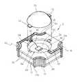
以下、本発明の好ましい実施例を図面を参照にさらに詳しく説明する。本発明によるアノダイジング絶縁層を有するLEDパッケージ1は、図2に図示された通り、アルミニウム材料からなる基板10が提供される。上記基板10は、相対的に低価かつ製作が容易なアルミニウム材料である。 Hereinafter, preferred embodiments of the present invention will be described in more detail with reference to the drawings. The
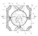
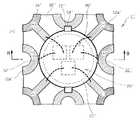
このような基板10には、一側面の中央に反射領域20が形成される。上記反射領域20は、基板10をエッチングして形成された凹溝からなるものであって、図3に図示された通り、以後に説明される光源30が安着する平らな中央反射領域22、即ちダイボンディング(Die Bonding)反射領域と、上記中央反射領域22を囲う傾斜反射領域24、即ちリフレクター(Reflector)反射面を形成する。 In such a
そして上記基板10の反射領域20には、その傾斜反射領域24に隣接して、四方に各々光源30を成すLED素子の電極をワイヤ40を通じて連結するための電極連結溝52と、以後に説明されるレンズ部70の位置を容易に設定して固定することが出来るレンズ固定溝54とを形成している。 An
上記電極連結溝52とレンズ固定溝54は、各々凹んで形成されたものであって、上記反射領域20を形成する傾斜反射領域24ほど深くはないが基板10の表面から凹んで形成された構造である。そして好ましくは、上記電極連結溝52の深さがレンズ固定溝54の深さよりやや深く形成される。このような構造を通じて上記電極連結溝52に上記ワイヤ40が容易に位置することが出来る。 The
さらに、上記電極連結溝52とレンズ固定溝54は、各々その数が本発明により制限されるのではない。 Further, the numbers of the
上記電極連結溝52の場合、光源30を成すLED素子のタイプによって一つもしくは2つで形成されることができ、また基板10上に装着されるLED素子の数に応じて多数形成されることが出来る。 The
そして上記レンズ固定溝54の場合にも、レンズ部70を容易に装着することが出来る基準溝を形成すれば良く、その形成数が本発明により制限されるのではない。 Also in the case of the
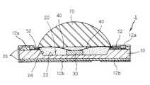
また上記基板10には、光源30に電源を供給するための電極パターン12a、12bが形成される。上記電極パターン12a、12bは、反射領域20が形成された基板10の一側面と、その反対面に形成されるもので、上記基板10の一側面に形成された電極パターン12aは、光源30であるLED素子と電気的連結を成すためのものであり、その反対面に形成された電極パターン12bは、本LEDパッケージが表面実装(SMD:Surface Mounted Device)型として他の基板(未図示)の表面に実装され電気的連結を成すためのパッドを形成するものである。 In addition,
また、上記のような一側面とその反対面の電極パターン12a、12bは、基板10を貫通する多数の貫通孔16を通じて電気的に連結されている。 Further, the
そして本発明によるアノダイジング絶縁層を有するLEDパッケージ1は、上記基板10上に装着され電極パターン12a、12bに電気的に連結されたLED素子の光源30を備え、上記電極パターン12a、12bと基板10との間に形成されたアノダイジング絶縁層35を備える。 The
上記アノダイジング絶縁層35は、上記電極パターン12a、12bが基板10に対して絶縁であるよう形成されたものであって、これは上記基板10をアノダイジング或いは陽極酸化処理して基板10を局所的或いは部分的に酸化アルミニウム(Al2O3)処理したものである。 The anodizing insulating
このようなアノダイジング絶縁層35は、伝熱性能はやや衰えるが絶縁性能は非常に優れたものであり、上記電極パターン12a、12bと基板10との間に形成され、上記電極パターン12a、12bが光源30の発光作用に必要な電源を供給することが出来るようにする。 The anodizing
一方、このようなアノダイジング絶縁層35は、上記電極連結溝52にも形成され基板10と電気的絶縁を成し、上記基板10の反射領域20には形成されないことにより、光源30の光を外部へ反射させるに如何なる障害も起こさないよう構成されたものである。 On the other hand, the anodizing insulating
そして、本発明によるアノダイジング絶縁層35を有するLEDパッケージ1は、上記基板10の光源30上に覆われるレンズ部70を含む構造である。上記レンズ部70は、一側面が膨らんだ断面形状を有するもので、図4に図示された通り、上記レンズ固定溝54に挿入可能な突起72を各々外面に形成している。 The
このような突起72は、上記レンズ固定溝54に各々対応するものであって、このような突起72とレンズ固定溝54とにより、作業者は基板10上にレンズ部70を付着しようとする場合、容易に装着位置もしくは基準位置を見つけることが出来る。このようなレンズ部70は、基板10上に透明な接着樹脂を通じて付着される。
上記のように基板10に付着されたレンズ部70は、図5に断面で図示された通り、基板10の電極連結溝52には位置しない。このように電極連結溝52にレンズ部70が位置しないことにより、電極連結溝52を通じたワイヤ40の配置が可能でワイヤ40の結線部分に障害を与えない。 As described above, the
上記のような本発明によるアノダイジング絶縁層を有するLEDパッケージ1の製造方法は下記のような工程段階で行われる。 The manufacturing method of the
本発明によるアノダイジング絶縁層を有するLEDパッケージ1の製造方法は、先ず、基板10の一側外表面をエッチングして反射領域20を形成する段階が行われる。 In the manufacturing method of the
上記反射領域20は、光源30が安着する平らな中央反射領域22と、上記中央反射領域22を囲う傾斜反射領域24とを形成し、上記反射領域20の形成段階は、上記反射領域20を成す傾斜反射領域24に隣接して、四方に各々光源30を成すLED素子の電極をワイヤ40を通じて連結するための電極連結溝52と、レンズ部70の位置を容易に設定して固定することが出来るレンズ固定溝54とを形成する段階をさらに含む。 The
このような電極連結溝52とレンズ固定溝54も全てエッチングを通じて形成することができる。 All of the
次に、上記基板10をアノダイジング処理して絶縁層35を形成する段階が行われる。このような場合、上記基板10は、上記反射領域20を除いた表面がアノダイジング処理され、酸化アルミニウム(Al2O3)の絶縁層35を基板10の上下面に形成することが出来る。 Next, the step of anodizing the
特に、上記電極連結溝52とレンズ固定溝54とにも各々絶縁層35が形成され、電極パターン12a、12bと光源30との電気的連結がより確実に成されるようにする。 In particular, an insulating
そして本発明は、上記基板10上に電極パターン12a、12bを形成する段階が行われる。このような場合、光源30を成すLED素子のタイプ、即ちLED素子のワイヤ40配線が上部面から両側に成される水平電極タイプであるか、または一つのワイヤ40配線がLED素子の上部面で成され、もう一つはLED素子の下部面で成される垂直電極であるなどのLED素子のタイプに応じて、それに合わせて電極パターン12a、12bを基板10上に形成することになる。 In the present invention, the step of forming the
また、このように電極パターン12a、12bを形成した後には、上記基板10に光源30を装着して電極パターン12a、12bに電気的連結を成す段階が行われる。このような段階はワイヤ40を通じた電気的連結を成す。 In addition, after the
そして上記のように光源30と電極パターン12a、12bとの電気的連結の後には、基板10にレンズ部70を装着する段階が行われる。このような段階では、基板10の反射領域20内に透明な接着樹脂を塗布した後、レンズ部70を付着させることになる。 Then, after the electrical connection between the
このような過程においてレンズ部70は、その外周面に形成された突起72を基板10に備えられたレンズ固定溝54に一致させた後、接着樹脂を用いて付着させることになり、このような作業工程は非常に容易に行われる。 In such a process, the
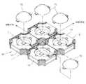
また本発明は、上記のように基板10とレンズ部70とを各々一つずつ別個で製作することが出来るが、これとは異なって図6に図示された通り、上記基板10を一つの大きな母基板80からダイシング処理して形成することが出来る。 Further, according to the present invention, the
即ち、一つの大きな母基板80を多数個の基板10に区切り、各々の基板10に対して上記のような製作工程を実施した後、多数のレンズ部70を各々の基板10に合わせて付着し、これらレンズ部70と基板10とを各々ダイシング処理して個別に本発明のLEDパッケージ1を構成することが出来る。 That is, one
このような母基板80を用いて多数のLEDパッケージ1を同時に生産する工程は、当業界では周知のことであるため、これに関するより詳しい説明は省略する。 Since the process of simultaneously producing a large number of
上記のような工程を通じて製作された本発明によるアノダイジング絶縁層を有するLEDパッケージ1は、基板10がアルミニウム材料からなり、このようなアルミニウム材料の基板10は、優れた伝熱特性を有するものであるため、LED素子の発光途中に発生する熱の高い放熱効果を得ることが出来る。 The
さらに、基板10に反射領域20をエッチングにより形成し、レンズ部70を基板10に容易に付着させることが出来るため、製作工程の単純化を通じて低価のLEDパッケージを得ることが出来る。 Furthermore, since the
図7および図8には、本発明の変形実施例によるアノダイジング絶縁層を有するLEDパッケージ1’が図示されている。 7 and 8 illustrate an LED package 1 'having an anodizing insulating layer according to a modified embodiment of the present invention.
図7および図8に図示された本発明のアノダイジング絶縁層を有するLEDパッケージ1’は、図2乃至図6に説明したLEDパッケージ1の構成と非常に類似であり、その技術思想を同一に有するため、以下では同一構成要素には同一参照符号を与え、それに添え字(’)を付けて区別する。 The
図7および図8に図示された本発明のアノダイジング絶縁層を有するLEDパッケージ1’は、白色光を発散するために多数個の、即ち青色LED素子、赤色LED素子および緑色LED素子を光源30’として備えている。 The
上記LED素子は、基板10’から(+)または(−)極性の電気端子が提供されてワイヤ40’により連結され、上記基板10’にアノダイジング絶縁層35’を通じて絶縁状態を維持する電極パターン12a’、12b’から上記基板10’の極性とは異なる(−)または(+)極性の電気端子が提供されてワイヤ40’を通じて光源30’に連結される。 The LED element is provided with a (+) or (−) polarity electrical terminal from the
そしてこのような多数個のLED素子は、その下部面で優れた発熱作用が得られるようにするため、ヒートスラグの役割をするアルミニウム放熱部65’を各々形成している。このようなヒートスラグ部分のアルミニウム放熱部65’は、アノダイジング絶縁層35’に囲まれて基板10’の他の部分と電気的に絶縁を成し、アルミニウム材料の優れた伝熱特性によりLED素子の優れた放熱効果を得ることが出来る。 Such a large number of LED elements are each formed with an aluminum
さらに、このようなLEDパッケージ1’も上記電極連結溝52’とレンズ固定溝54’とに各々絶縁層35’が形成され、電極パターン12a’、12b’と光源30’との電気的連結がさらに確実に行われるようにする。 Further, in the
図9および図10には、本発明のまた異なる変形実施例によるアノダイジング絶縁層を有するLEDパッケージ1’’が図示されている。 FIGS. 9 and 10 show an
このような構造も図2乃至図6に説明したLEDパッケージ1の構成に非常に類似で、その技術思想を同一に有するため、以下では同一構成要素には同一参照符号を与え、それに添え字(’’)を付けて区別する。 Such a structure is also very similar to the configuration of the
図9および図10に図示された本発明のアノダイジング絶縁層を有するLEDパッケージ1’’は、白色光を発散するために多数個の、即ち青色LED素子、赤色LED素子および緑色LED素子を備え、これは何れも基板10’’上にアノダイジング絶縁層35’’を通じて絶縁状態を維持する電極パターン12a’’、12b’’から(−)または(+)極性の電気端子が提供されてワイヤ40’’により連結された構造である。 The LED package 1 '' having an anodizing insulating layer of the present invention illustrated in FIGS. 9 and 10 includes a plurality of blue, red, and green LED elements to emit white light, In this case, the
このような多数個のLED素子も、その下部面で優れた発熱作用が得られるようにするため、ヒートスラグの役割をするアルミニウム放熱部65’’を各々形成している。このようなヒートスラグ部分のアルミニウム放熱部65’’もアルミニウム材料の優れた伝熱特性によりLED素子の優れた放熱効果を得ることが出来る。 Such a large number of LED elements are each formed with an aluminum
そしてこのようなLEDパッケージ1’’も上記電極連結溝52’’とレンズ固定溝54’’とに各々絶縁層35’’が形成され、電極パターン12a’’、12b’’と光源30’’との電気的連結がより確実に行われる。 Such an LED package 1 '' is also formed with an insulating layer 35 '' in the electrode connecting groove 52 '' and the lens fixing groove 54 '', respectively, and
本発明は、特定の実施例に関して図示し説明したが、これは単なる例示として本発明を説明するために記載されたものであって、本発明をこのような特定構造に制限するのではない。当業界において通常の知識を有している者であれば、以下の特許請求の範囲に記載された本発明の思想および領域を外れない範囲内で本発明を多様に修正および変更できることが分かる。ところが、このような修正および変形構造は何れも本発明の権利範囲内に含まれることを明らかにする。 Although the present invention has been illustrated and described with respect to particular embodiments, this has been described by way of illustration only and not as a limitation of the present invention. Those skilled in the art will recognize that the present invention can be variously modified and changed without departing from the spirit and scope of the present invention described in the following claims. However, it will be made clear that all such modifications and variations are within the scope of the present invention.
1 本発明によるLEDパッケージ
10 基板
12a、12b 電極パターン
16 貫通孔(Via)
20 反射領域
22 中央反射領域
24 傾斜反射領域
30、30’、30’’ 光源
35、35’、35’’ アノダイジング絶縁層
40 ワイヤ
52 電極連結溝
54 レンズ固定溝
65’、65’’ アルミニウム放熱部
70 レンズ部
72 突起
80 母基板
200 従来のLEDパッケージ
205 電極パターン
210 基板
215 LED素子
220 反射部材
222 反射面DESCRIPTION OF
20
Claims (11)
Translated fromJapanese前記電極パターンと前記基板との間に形成されたアノダイジング絶縁層と、
前記基板の上面の凹溝に形成された前記反射領域上に装着され前記電極パターンに電気的に連結された光源と、
前記光源のLED素子の下部面に形成されて放熱性能を向上させるアルミニウム放熱部と、
前記基板の光源上に覆われるレンズ部と、を含み、
前記基板の下面に形成された前記アノダイジング絶縁層は一部が前記凹溝に露出されて前記光源が装着され、
前記アルミニウム放熱部は、前記アノダイジング絶縁層に囲まれて前記基板と電気的に絶縁される
LEDパッケージ。A substrate made of an aluminum material and having a reflective region and an electrode pattern formed thereon;
An anodizing insulating layer formed between the electrode pattern and the substrate;
A light source mounted on the reflective regionformed in a concave groove on the upper surface of the substrate and electrically connected to the electrode pattern;
An aluminum heat dissipating part formed on the lower surface of the LED element of the light source to improve heat dissipating performance;
A lens part covered on the light source of the substrate,
A part of the anodizing insulating layer formed on the lower surface of the substrate is exposed in the concave groove, and the light source is mounted.
The aluminum heat dissipating part is surrounded by the anodizing insulating layer and electrically insulated from the substrate.
前記基板をアノダイジング処理して前記基板の上面と下面にそれぞれアノダイジング絶縁層を形成する段階と、
前記絶縁層に囲まれて前記基板と電気的に絶縁されるアルミニウム放熱部を前記絶縁層内に形成する段階と、
前記絶縁層上に電極パターンを形成する段階と、
前記アルミニウム放熱部上に光源を装着し前記電極パターンに電気的連結を成す段階と、
前記基板にレンズ部を装着する段階と、を含み、
前記基板の下面に形成された前記アノダイジング絶縁層は一部が前記凹溝に露出されて前記光源が装着され、前記アルミニウム放熱部は上面が露出されて前記アノダイジング絶縁層内に形成され、前記光源は前記アルミニウム放熱部の露出された上面に装着されることを特徴とするLEDパッケージの製造方法。Etching the outer surface on one side of the substrate to form a reflective region of thegroove ,
Anodizing the substrate to formanodizing insulating layerson the upper and lower surfaces of the substrate, respectively .
Forming an aluminum heat dissipating portion in the insulating layer surrounded by the insulating layer and electrically insulated from the substrate;
Forming an electrode pattern on the insulating layer;
Mounting a light source on the aluminum heat dissipating part and electrically connecting the electrode pattern;
Look including the the steps of mounting the lens portion on thesubstrate,
A part of the anodizing insulating layer formed on the lower surface of the substrate is exposed in the concave groove and the light source is mounted, and the aluminum heat dissipating part is formed in the anodizing insulating layer with the upper surface exposed. Is mounted on the exposed upper surface of the aluminum heat dissipating part .
Applications Claiming Priority (2)
| Application Number | Priority Date | Filing Date | Title |
|---|---|---|---|
| KR10-2006-0031093 | 2006-04-05 | ||
| KR1020060031093AKR100764432B1 (en) | 2006-04-05 | 2006-04-05 | LED package having anodizing insulation layer and manufacturing method thereof |
Publications (2)
| Publication Number | Publication Date |
|---|---|
| JP2007281468A JP2007281468A (en) | 2007-10-25 |
| JP4787783B2true JP4787783B2 (en) | 2011-10-05 |
Family
ID=38574270
Family Applications (1)
| Application Number | Title | Priority Date | Filing Date |
|---|---|---|---|
| JP2007097039AActiveJP4787783B2 (en) | 2006-04-05 | 2007-04-03 | LED package having anodizing insulating layer and manufacturing method thereof |
Country Status (5)
| Country | Link |
|---|---|
| US (2) | US8030762B2 (en) |
| JP (1) | JP4787783B2 (en) |
| KR (1) | KR100764432B1 (en) |
| CN (2) | CN101714597B (en) |
| TW (1) | TWI383517B (en) |
Families Citing this family (49)
| Publication number | Priority date | Publication date | Assignee | Title |
|---|---|---|---|---|
| JP5401025B2 (en)* | 2007-09-25 | 2014-01-29 | 三洋電機株式会社 | Light emitting module and manufacturing method thereof |
| US8360593B2 (en)* | 2007-09-28 | 2013-01-29 | Seoul Semiconductor Co., Ltd. | LED package and back light unit using the same |
| JP3142406U (en)* | 2008-03-31 | 2008-06-12 | サンケン電気株式会社 | Semiconductor light emitting device and semiconductor light emitting unit |
| KR100939273B1 (en) | 2008-03-31 | 2010-01-29 | 성균관대학교산학협력단 | Multi-layer manufacturing method using anodization |
| KR100998010B1 (en) | 2008-04-28 | 2010-12-03 | 삼성엘이디 주식회사 | Light emitting device package and its manufacturing method |
| TWI488329B (en)* | 2008-05-15 | 2015-06-11 | Everlight Electronics Co Ltd | Circuit substrate and LED package |
| CN102142423B (en)* | 2008-05-16 | 2014-11-26 | 亿光电子工业股份有限公司 | Circuit substrate and LED packaging |
| AT506709B1 (en)* | 2008-05-30 | 2009-11-15 | Kuster Martin | LAMPS |
| DE102008039147A1 (en)* | 2008-05-30 | 2009-12-03 | Osram Opto Semiconductors Gmbh | Optoelectronic module and optoelectronic device |
| KR101021245B1 (en)* | 2008-08-07 | 2011-03-11 | 이동규 | Light emitting diode device |
| JP5204618B2 (en)* | 2008-10-21 | 2013-06-05 | 電気化学工業株式会社 | Light emitting element mounting substrate, light emitting element package, and method of manufacturing light emitting element mounting substrate |
| KR101077264B1 (en)* | 2009-02-17 | 2011-10-27 | (주)포인트엔지니어링 | Substrate for optical device, optical device package having the same and menufacturing method thereof |
| KR101114592B1 (en)* | 2009-02-17 | 2012-03-09 | 엘지이노텍 주식회사 | Lighting emitting device and fabrication method thereof |
| KR101092063B1 (en)* | 2009-04-28 | 2011-12-12 | 엘지이노텍 주식회사 | Light emitting device package and method for fabricating the same |
| WO2011034304A2 (en)* | 2009-09-17 | 2011-03-24 | 주식회사 포인트 엔지니어링 | Substrate for an optical device, optical device, and method for manufacturing same |
| WO2011034259A1 (en) | 2009-09-17 | 2011-03-24 | 포인트엔지니어링 | Optical element substrate, optical element device, and method for manufacturing same |
| TWI416771B (en)* | 2009-10-01 | 2013-11-21 | Everlight Electronics Co Ltd | Light-emitting diode |
| KR101022485B1 (en)* | 2009-10-20 | 2011-03-15 | (주)브이엘시스템 | Heat dissipation structure of LED lighting device using heat pipe module |
| KR101053835B1 (en) | 2010-04-29 | 2011-08-03 | 에스티플렉스 주식회사 | LED heat dissipation structure |
| US8664538B2 (en)* | 2010-04-30 | 2014-03-04 | Wavenics Inc. | Terminal-integrated metal base package module and terminal-integrated metal base packaging method |
| KR101662038B1 (en)* | 2010-05-07 | 2016-10-05 | 삼성전자 주식회사 | Chip package |
| WO2011155783A1 (en)* | 2010-06-11 | 2011-12-15 | (주)브이엘시스템 | Heat-dissipating structure of an led illuminating device, using a heat pipe module |
| KR101114197B1 (en)* | 2010-08-09 | 2012-02-22 | 엘지이노텍 주식회사 | Light emitting device and lighting system having same |
| CN102447034B (en)* | 2010-09-30 | 2014-05-07 | 展晶科技(深圳)有限公司 | LED (light emitting diode) packaging structure and manufacturing method thereof |
| KR101081216B1 (en) | 2011-03-09 | 2011-11-07 | 박상훈 | Removable Lens for LED Package |
| WO2012148020A1 (en)* | 2011-04-28 | 2012-11-01 | 주식회사 이넥트론 | Method for forming a nanodiamond-impregnated dielectric layer for a highly heat dissipating metal substrate |
| USD700584S1 (en)* | 2011-07-06 | 2014-03-04 | Cree, Inc. | LED component |
| FR2984679B1 (en)* | 2011-12-15 | 2015-03-06 | Valeo Sys Controle Moteur Sas | THERMALLY CONDUCTIVE AND ELECTRICALLY INSULATING CONNECTION BETWEEN AT LEAST ONE ELECTRONIC COMPONENT AND A RADIATOR IN ALL OR METALLIC PORTION |
| CN102629658A (en)* | 2011-12-22 | 2012-08-08 | 南宁市明锐电子科技有限公司 | Radiator of large power LED reflection cup |
| KR101516358B1 (en)* | 2012-03-06 | 2015-05-04 | 삼성전자주식회사 | Light Emitting Device |
| CN103378252B (en)* | 2012-04-16 | 2016-01-06 | 展晶科技(深圳)有限公司 | Light emitting diode module |
| USD718258S1 (en)* | 2012-09-02 | 2014-11-25 | Cree, Inc. | LED package |
| KR101975190B1 (en)* | 2013-06-28 | 2019-05-07 | 엘지디스플레이 주식회사 | Light emitting diode package |
| US10167566B2 (en) | 2013-09-05 | 2019-01-01 | Sharp Kabushiki Kaisha | Substrate for light emitting device, light emitting device, and method for manufacturing substrate for light emitting device |
| KR101501019B1 (en)* | 2013-12-11 | 2015-03-12 | 주식회사 루멘스홀딩스 | Substrate apparatus having align mark and light emitting device package |
| KR101668353B1 (en)* | 2014-11-03 | 2016-10-21 | (주)포인트엔지니어링 | Chip Substrate and Chip Package Module |
| CN104409620A (en)* | 2014-12-17 | 2015-03-11 | 木林森股份有限公司 | Small-sized LED lamp bead set and lamp beads |
| CN104409451A (en)* | 2014-12-17 | 2015-03-11 | 木林森股份有限公司 | Bracket set of small-sized LED lamp beads and brackets |
| US10429509B2 (en) | 2014-12-24 | 2019-10-01 | Stmicroelectronics Pte Ltd. | Molded proximity sensor |
| KR102212340B1 (en)* | 2015-01-02 | 2021-02-05 | (주)포인트엔지니어링 | Chip substrate comprising junction groove in lens insert |
| US20160307881A1 (en)* | 2015-04-20 | 2016-10-20 | Advanced Semiconductor Engineering, Inc. | Optical sensor module and method for manufacturing the same |
| CN110890353B (en)* | 2015-09-08 | 2023-12-26 | 首尔伟傲世有限公司 | Light emitting diode package |
| CN206708739U (en)* | 2016-06-30 | 2017-12-05 | 欧普照明股份有限公司 | A kind of LED module and LED illumination lamp |
| CN111446353A (en)* | 2019-01-16 | 2020-07-24 | 株式会社辉元 | Ceramic light emitting diode package and method of manufacturing the same |
| KR102575288B1 (en)* | 2019-12-16 | 2023-09-06 | 주식회사 아모센스 | Semiconductor package and manufacturing method thereof |
| CN111379981A (en)* | 2020-04-28 | 2020-07-07 | 东莞市索菲电子科技有限公司 | Light-concentrating high-color-rendering-index high-brightness surface-mounted LED |
| JP7536676B2 (en)* | 2021-02-10 | 2024-08-20 | キオクシア株式会社 | Anodizing apparatus and anodizing method |
| CN114824049B (en)* | 2022-03-25 | 2025-08-19 | 厦门普为光电科技有限公司 | Light emitting diode with reflecting frame |
| KR102512957B1 (en)* | 2022-06-08 | 2023-03-23 | 주식회사 비에스테크닉스 | Assemply-type Block With LED Module And Manufacturing Method Of The Same |
Family Cites Families (24)
| Publication number | Priority date | Publication date | Assignee | Title |
|---|---|---|---|---|
| DE58909888C5 (en)* | 1989-05-31 | 2017-03-02 | Osram Gesellschaft mit beschränkter Haftung | A method of manufacturing a surface mount opto-device and surface mount opto-device |
| US5631190A (en)* | 1994-10-07 | 1997-05-20 | Cree Research, Inc. | Method for producing high efficiency light-emitting diodes and resulting diode structures |
| US6204523B1 (en)* | 1998-11-06 | 2001-03-20 | Lumileds Lighting, U.S., Llc | High stability optical encapsulation and packaging for light-emitting diodes in the green, blue, and near UV range |
| US6480389B1 (en)* | 2002-01-04 | 2002-11-12 | Opto Tech Corporation | Heat dissipation structure for solid-state light emitting device package |
| WO2003065464A1 (en) | 2002-01-28 | 2003-08-07 | Nichia Corporation | Nitride semiconductor device having support substrate and its manufacturing method |
| CN100338786C (en)* | 2002-06-19 | 2007-09-19 | 三垦电气株式会社 | Semiconductor light-emitting device, manufacturing method thereof, and reflector for semiconductor light-emitting device |
| JP4241184B2 (en)* | 2002-07-25 | 2009-03-18 | パナソニック電工株式会社 | Photoelectric component |
| KR100567559B1 (en) | 2002-07-25 | 2006-04-05 | 마츠시다 덴코 가부시키가이샤 | Device with photoelectric element |
| US7170151B2 (en)* | 2003-01-16 | 2007-01-30 | Philips Lumileds Lighting Company, Llc | Accurate alignment of an LED assembly |
| JP4281363B2 (en)* | 2003-01-20 | 2009-06-17 | パナソニック電工株式会社 | Wiring board and light emitting device |
| CN2613054Y (en)* | 2003-03-12 | 2004-04-21 | 兴华电子工业股份有限公司 | Substrate Structure of Light Emitting Diode Wafer |
| KR20040092512A (en)* | 2003-04-24 | 2004-11-04 | (주)그래픽테크노재팬 | A semiconductor light emitting device with reflectors having a cooling function |
| WO2004102685A1 (en)* | 2003-05-14 | 2004-11-25 | Nano Packaging Technology, Inc. | Light emitting device, package structure thereof and manufacturing method thereof |
| JP2005064047A (en) | 2003-08-13 | 2005-03-10 | Citizen Electronics Co Ltd | Light emitting diode |
| US7183587B2 (en) | 2003-09-09 | 2007-02-27 | Cree, Inc. | Solid metal block mounting substrates for semiconductor light emitting devices |
| KR100555174B1 (en)* | 2003-09-29 | 2006-03-03 | 바이오닉스(주) | Manufacturing method of high output LED package and high output LED package using same |
| JP2005175048A (en)* | 2003-12-09 | 2005-06-30 | Sanken Electric Co Ltd | Semiconductor light emitting device |
| CN1684278A (en) | 2004-04-15 | 2005-10-19 | 联欣光电股份有限公司 | Packaging structure and packaging method of a light emitting diode |
| JP2006012868A (en)* | 2004-06-22 | 2006-01-12 | Toshiba Corp | Package for semiconductor light emitting device and semiconductor light emitting device using the same |
| JP2006049442A (en)* | 2004-08-02 | 2006-02-16 | Sharp Corp | Semiconductor light emitting device and manufacturing method thereof |
| JP2006060070A (en)* | 2004-08-20 | 2006-03-02 | Kyoritsu Elex Co Ltd | Light-emitting diode, package therefor, and method for manufacturing the package |
| JP4593201B2 (en)* | 2004-08-20 | 2010-12-08 | 日立化成工業株式会社 | Chip component type light emitting device and wiring board therefor |
| CN100380694C (en)* | 2004-12-10 | 2008-04-09 | 北京大学 | A packaging method for flip-chip LED chips |
| US20060124953A1 (en)* | 2004-12-14 | 2006-06-15 | Negley Gerald H | Semiconductor light emitting device mounting substrates and packages including cavities and cover plates, and methods of packaging same |
- 2006
- 2006-04-05KRKR1020060031093Apatent/KR100764432B1/enactiveActive
- 2007
- 2007-03-30TWTW096111189Apatent/TWI383517B/enactive
- 2007-04-03CNCN2009101794426Apatent/CN101714597B/enactiveActive
- 2007-04-03JPJP2007097039Apatent/JP4787783B2/enactiveActive
- 2007-04-03CNCN2007100922606Apatent/CN101051665B/enactiveActive
- 2007-04-05USUS11/730,966patent/US8030762B2/enactiveActive
- 2011
- 2011-08-29USUS13/220,258patent/US8304279B2/enactiveActive
Also Published As
| Publication number | Publication date |
|---|---|
| CN101714597B (en) | 2011-11-16 |
| TWI383517B (en) | 2013-01-21 |
| CN101714597A (en) | 2010-05-26 |
| CN101051665B (en) | 2010-12-15 |
| JP2007281468A (en) | 2007-10-25 |
| CN101051665A (en) | 2007-10-10 |
| US8304279B2 (en) | 2012-11-06 |
| US8030762B2 (en) | 2011-10-04 |
| US20070235743A1 (en) | 2007-10-11 |
| KR100764432B1 (en) | 2007-10-05 |
| US20110312109A1 (en) | 2011-12-22 |
| TW200802975A (en) | 2008-01-01 |
Similar Documents
| Publication | Publication Date | Title |
|---|---|---|
| JP4787783B2 (en) | LED package having anodizing insulating layer and manufacturing method thereof | |
| JP5175488B2 (en) | LED package having multilayer reflective surface structure | |
| JP4674221B2 (en) | Light emitting diode package | |
| JP4192742B2 (en) | Light emitting device | |
| JP4808550B2 (en) | Light emitting diode light source device, lighting device, display device, and traffic signal device | |
| JP2006005290A (en) | Light emitting diode | |
| JP2005158957A (en) | Light emitting device | |
| JP2004172170A (en) | High brightness light emitting device and method of manufacturing the same | |
| JPH11298048A (en) | Led mounting board | |
| JP7094182B2 (en) | Lamp unit | |
| JP4254470B2 (en) | Light emitting device | |
| KR20100117451A (en) | Pcb with radiation hole and led illumination device using it | |
| JP2006147865A (en) | Light emitting element mounting substrate and method for manufacturing the same, light emitting element module and method for manufacturing the same, display device, lighting device, and traffic signal device | |
| JP2004146411A (en) | High luminance light emitting device and its manufacturing method | |
| JP2000236111A (en) | Light source equipment | |
| JP4655735B2 (en) | LED unit | |
| JP2000235808A (en) | Light source device | |
| TWI546987B (en) | Illuminating device | |
| JP5179311B2 (en) | Light emitting device | |
| JP5999341B2 (en) | Light emitting device and lighting device | |
| KR20130007473A (en) | Led pcb substrate, pcb, led unit, lighting and its manufacture | |
| JP4954664B2 (en) | Light emitting element mounting substrate, light emitting element mounting package, and surface light source device | |
| JP2009021383A (en) | Electronic component | |
| JP2006269758A (en) | Light emitting device mounting enamel substrate, light emitting device module, display device, lighting device, and traffic signal device | |
| JP2012009631A (en) | Light emitting device and lighting system |
Legal Events
| Date | Code | Title | Description |
|---|---|---|---|
| A977 | Report on retrieval | Free format text:JAPANESE INTERMEDIATE CODE: A971007 Effective date:20100827 | |
| A131 | Notification of reasons for refusal | Free format text:JAPANESE INTERMEDIATE CODE: A131 Effective date:20100914 | |
| A711 | Notification of change in applicant | Free format text:JAPANESE INTERMEDIATE CODE: A711 Effective date:20100930 | |
| A521 | Request for written amendment filed | Free format text:JAPANESE INTERMEDIATE CODE: A523 Effective date:20101214 | |
| A02 | Decision of refusal | Free format text:JAPANESE INTERMEDIATE CODE: A02 Effective date:20110125 | |
| A521 | Request for written amendment filed | Free format text:JAPANESE INTERMEDIATE CODE: A523 Effective date:20110525 | |
| A911 | Transfer to examiner for re-examination before appeal (zenchi) | Free format text:JAPANESE INTERMEDIATE CODE: A911 Effective date:20110531 | |
| TRDD | Decision of grant or rejection written | ||
| A01 | Written decision to grant a patent or to grant a registration (utility model) | Free format text:JAPANESE INTERMEDIATE CODE: A01 Effective date:20110628 | |
| A01 | Written decision to grant a patent or to grant a registration (utility model) | Free format text:JAPANESE INTERMEDIATE CODE: A01 | |
| A61 | First payment of annual fees (during grant procedure) | Free format text:JAPANESE INTERMEDIATE CODE: A61 Effective date:20110715 | |
| R150 | Certificate of patent or registration of utility model | Ref document number:4787783 Country of ref document:JP Free format text:JAPANESE INTERMEDIATE CODE: R150 Free format text:JAPANESE INTERMEDIATE CODE: R150 | |
| FPAY | Renewal fee payment (event date is renewal date of database) | Free format text:PAYMENT UNTIL: 20140722 Year of fee payment:3 | |
| FPAY | Renewal fee payment (event date is renewal date of database) | Free format text:PAYMENT UNTIL: 20140722 Year of fee payment:3 | |
| S111 | Request for change of ownership or part of ownership | Free format text:JAPANESE INTERMEDIATE CODE: R313111 | |
| S631 | Written request for registration of reclamation of domicile | Free format text:JAPANESE INTERMEDIATE CODE: R313631 | |
| FPAY | Renewal fee payment (event date is renewal date of database) | Free format text:PAYMENT UNTIL: 20140722 Year of fee payment:3 | |
| R371 | Transfer withdrawn | Free format text:JAPANESE INTERMEDIATE CODE: R371 | |
| S111 | Request for change of ownership or part of ownership | Free format text:JAPANESE INTERMEDIATE CODE: R313111 | |
| S631 | Written request for registration of reclamation of domicile | Free format text:JAPANESE INTERMEDIATE CODE: R313631 | |
| S633 | Written request for registration of reclamation of name | Free format text:JAPANESE INTERMEDIATE CODE: R313633 | |
| FPAY | Renewal fee payment (event date is renewal date of database) | Free format text:PAYMENT UNTIL: 20140722 Year of fee payment:3 | |
| R371 | Transfer withdrawn | Free format text:JAPANESE INTERMEDIATE CODE: R371 | |
| FPAY | Renewal fee payment (event date is renewal date of database) | Free format text:PAYMENT UNTIL: 20140722 Year of fee payment:3 | |
| S111 | Request for change of ownership or part of ownership | Free format text:JAPANESE INTERMEDIATE CODE: R313111 | |
| S531 | Written request for registration of change of domicile | Free format text:JAPANESE INTERMEDIATE CODE: R313531 | |
| S533 | Written request for registration of change of name | Free format text:JAPANESE INTERMEDIATE CODE: R313533 | |
| FPAY | Renewal fee payment (event date is renewal date of database) | Free format text:PAYMENT UNTIL: 20140722 Year of fee payment:3 | |
| R350 | Written notification of registration of transfer | Free format text:JAPANESE INTERMEDIATE CODE: R350 | |
| R250 | Receipt of annual fees | Free format text:JAPANESE INTERMEDIATE CODE: R250 | |
| R250 | Receipt of annual fees | Free format text:JAPANESE INTERMEDIATE CODE: R250 | |
| R250 | Receipt of annual fees | Free format text:JAPANESE INTERMEDIATE CODE: R250 | |
| R250 | Receipt of annual fees | Free format text:JAPANESE INTERMEDIATE CODE: R250 | |
| R250 | Receipt of annual fees | Free format text:JAPANESE INTERMEDIATE CODE: R250 | |
| R250 | Receipt of annual fees | Free format text:JAPANESE INTERMEDIATE CODE: R250 | |
| R250 | Receipt of annual fees | Free format text:JAPANESE INTERMEDIATE CODE: R250 | |
| R250 | Receipt of annual fees | Free format text:JAPANESE INTERMEDIATE CODE: R250 | |
| R250 | Receipt of annual fees | Free format text:JAPANESE INTERMEDIATE CODE: R250 | |
| R250 | Receipt of annual fees | Free format text:JAPANESE INTERMEDIATE CODE: R250 | |
| R250 | Receipt of annual fees | Free format text:JAPANESE INTERMEDIATE CODE: R250 | |
| R250 | Receipt of annual fees | Free format text:JAPANESE INTERMEDIATE CODE: R250 |