JP4784052B2 - Solid-state image sensor - Google Patents
Solid-state image sensorDownload PDFInfo
- Publication number
- JP4784052B2 JP4784052B2JP2004197969AJP2004197969AJP4784052B2JP 4784052 B2JP4784052 B2JP 4784052B2JP 2004197969 AJP2004197969 AJP 2004197969AJP 2004197969 AJP2004197969 AJP 2004197969AJP 4784052 B2JP4784052 B2JP 4784052B2
- Authority
- JP
- Japan
- Prior art keywords
- solid
- diffractive optical
- light
- optical element
- light receiving
- Prior art date
- Legal status (The legal status is an assumption and is not a legal conclusion. Google has not performed a legal analysis and makes no representation as to the accuracy of the status listed.)
- Expired - Fee Related
Links
Images


Landscapes
- Diffracting Gratings Or Hologram Optical Elements (AREA)
- Solid State Image Pick-Up Elements (AREA)
- Transforming Light Signals Into Electric Signals (AREA)
- Light Receiving Elements (AREA)
Description
Translated fromJapanese本発明は、デジタルスチルカメラ、デジタルビデオカメラ、携帯電話に組み込まれるカメラ、防犯用監視カメラなどに用いられる固体撮像素子に関するものである。 The present invention relates to a solid-state imaging device used for a digital still camera, a digital video camera, a camera incorporated in a mobile phone, a security surveillance camera, and the like.
近年、パーソナルコンピュータ、携帯電話の普及に伴い、パーソナルコンピュータ用の液晶ディスプレイ、携帯電話用の液晶ディスプレイの需要が増加する傾向にあり、これらと関連して用いられる撮像装置、例えば、デジタルスチルカメラ、デジタルビデオカメラ、携帯電話に組み込まれるカメラ、防犯用監視カメラなどの撮像装置も益々その用途が広くなり、需要が増加する傾向にある。
これら撮像装置には、通常、CCD等の受光素子として固体撮像素子が用いられているが、半導体製造技術の進歩とともに、固体撮像素子の画素の微細化が一段と進み、益々、撮影画像の高画質化が求められている。
このような中、CCD等の固体撮像素子を用いた固体撮像装置においては、更に高感度化が求められているが、デバイスの制約上、固体撮像素子の受光部である画素を隙間なく並べることができない。そこで、限定された面積の固体撮像素子の画素への集光率を向上させるために、マイクロレンズアレイを固体撮像素子の前に設けて、固体撮像素子の各画素に入射する光量を効率的に得て、感度を向上させる方法が、感度を増す方法の1つとして、広く知られている。(例えば、特許文献1参照)。In recent years, with the spread of personal computers and mobile phones, there is a tendency for demand for liquid crystal displays for personal computers and liquid crystal displays for mobile phones to increase. Imaging devices used in connection therewith, such as digital still cameras, Imaging devices such as digital video cameras, cameras incorporated in mobile phones, security surveillance cameras, and the like are becoming increasingly widespread, and demand is increasing.
In these image pickup devices, solid-state image pickup devices are usually used as light-receiving elements such as CCDs. However, with the advancement of semiconductor manufacturing technology, the pixels of solid-state image pickup devices are becoming increasingly finer, and the image quality of captured images is increasing. Is required.
Under such circumstances, in a solid-state imaging device using a solid-state imaging device such as a CCD, higher sensitivity is required. However, due to device limitations, pixels that are light-receiving portions of the solid-state imaging device are arranged without gaps. I can't. Therefore, in order to improve the light collection rate to the pixels of the solid-state image sensor with a limited area, a microlens array is provided in front of the solid-state image sensor, and the amount of light incident on each pixel of the solid-state image sensor is efficiently reduced. Thus, a method for improving the sensitivity is widely known as one of the methods for increasing the sensitivity. (For example, refer to Patent Document 1).
一方、固体撮像装置をカラー化する方法として、形成したカラーフィルターを固体撮像装置に後づけする接着方式に代わって、固体撮像装置が形成された基板上に直接カラーフィルターを形成するオンチップカラーフィルター方式が主流となっている。(例えば、特許文献2参照)。 On the other hand, as a method for colorizing a solid-state imaging device, an on-chip color filter that directly forms a color filter on a substrate on which the solid-state imaging device is formed, instead of an adhesion method in which the formed color filter is retrofitted to the solid-state imaging device The method has become mainstream. (For example, refer to Patent Document 2).
以下、従来の固体撮像装置について、図面を参照しながら説明する。
第1図は、従来の固体撮像装置の構造を示す部分断面図である。第1図に示すように、固体撮像装置は、その表面に受光素子(2)、遮光層(3)などが形成された半導体基板(1)上に、平坦化層(4)、原色のカラーフィルター(5)、平坦化層(7)、マイクロレンズ(6)が順次形成されたものである。このような構造により、マイクロレンズとカラーフィルターを備えた固体撮像装置を実現していた。Hereinafter, a conventional solid-state imaging device will be described with reference to the drawings.
FIG. 1 is a partial cross-sectional view showing the structure of a conventional solid-state imaging device. As shown in FIG. 1, the solid-state imaging device has a planarizing layer (4), a primary color on a semiconductor substrate (1) having a light receiving element (2), a light shielding layer (3) and the like formed on the surface thereof. A filter (5), a flattening layer (7), and a microlens (6) are sequentially formed. With such a structure, a solid-state imaging device including a microlens and a color filter has been realized.
次にその動作を説明する。最上層であるマイクロレンズ(6)に入射した光は集束され、カラーフィルター(5)により各々の分光透過率特性を有する光に分解される。そしてその分解された光は各カラーフィルターセル(5R、5G、5B)下の受光素子(2)に入射する。受光素子(2)に入射した光は電気信号に変換され、カラー画像を提供する固体撮像装置として動作する。
このように、従来から固体撮像素子の前にマイクロレンズアレイを設けて、固体撮像素子の各画素に入射光を集光させることは広く知られているが、固体撮像素子の画素の微細化に伴い、レンズ形状も画素と同サイズに縮小する必要があり、現在では4μm以下のレンズが求められている。一方、光の波長は、青色が450nm、緑色が550nm、赤色が630nmであり、レンズのサイズは光の波長に近づいているため、レンズの設計は困難であり、光を効率よく集光できるレンズとはならない。たとえレンズ形状を正しく作成できたとしても光の波動効果があり、屈折の現象が当てはまらない場合が生じる。更に、光の波長サイズの凹凸は、屈折現象を超えて電磁場解析を必要とする領域となっている。例えば、MOTHEYEに代表される光の波長オーダーの凹凸は、透過光を与えるのみであり、光を集光しない。 As described above, it has been widely known that a microlens array is provided in front of a solid-state image sensor to collect incident light on each pixel of the solid-state image sensor. Along with this, it is necessary to reduce the lens shape to the same size as the pixel. At present, a lens of 4 μm or less is demanded. On the other hand, the wavelengths of light are 450 nm for blue, 550 nm for green, and 630 nm for red, and the lens size is close to the wavelength of the light. Therefore, the lens design is difficult, and the lens can collect light efficiently. It will not be. Even if the lens shape can be created correctly, there is a case where there is a wave effect of light and the phenomenon of refraction does not apply. Furthermore, the unevenness of the wavelength size of light is a region that requires an electromagnetic field analysis beyond the refraction phenomenon. For example, the unevenness of the wavelength order of light represented by MOTHEYE only gives transmitted light and does not collect light.
本発明は従来技術のこのような状況の下になされたものであり、固体撮像素子の高解像度化に伴い、各画素及びレンズのサイズは微小となり、レンズのサイズが光の波長に近くなるに従い、光の波としての性質の影響で期待通りの集光効果が得られなくなりつつあるという課題を解決するため、従来の固体撮像素子に設けられたマイクロレンズアレイに換えて、光を効率良く集光できる回折光学素子を設けた固体撮像素子を提供することである。 The present invention has been made under such circumstances of the prior art, and as the resolution of a solid-state image sensor increases, the size of each pixel and lens becomes smaller, and as the lens size becomes closer to the wavelength of light. In order to solve the problem that the expected light collection effect cannot be obtained due to the influence of the properties of light waves, instead of using a microlens array provided in a conventional solid-state image sensor, light is collected efficiently. To provide a solid-state imaging device provided with a diffractive optical element capable of emitting light.
本発明の固体撮像素子は、表面に複数の受光素子が形成された半導体基板と、この半導体基板の上方に配置され、前記複数の受光素子に光を集光する回折光学素子とを有し、前記回折光学素子は、入射光に対して異なる位相を与える同一形状の微細な2種の正方形領域が、交互に市松格子状として配列され、前記受光素子は、半導体基板表面に格子状に配列され、前記回折光学素子の各々の正方形領域と各々の受光素子が対応して配置されており、且つ、前記回折光学素子の正方形領域は、各受光素子に対して1つおきに凸部を形成していることを特徴とするものである。The solid-state imaging device of the present invention includes a semiconductor substrate having a plurality of light receiving elements formed on a surface thereof, and a diffractive optical element that is disposed above the semiconductor substrate and collects light on the plurality of light receiving elements, In the diffractive optical element, two kinds of fine square regions having the same shape that give different phases to incident light are alternately arranged in a checkered lattice shape, and the light receiving elements are arranged in a lattice shape on the surface of the semiconductor substrate. Each of the square regions of the diffractive optical element and each of the light receiving elements are arranged correspondingly, and the square region of the diffractive optical element forms a convex portion for every other light receiving element. It is characterized by that.
また、この固体撮像素子の前記回折光学素子は、垂直に入射する可視領域波長の光に対して位相0を与える領域と位相0.65π〜1.87πを与える領域が、交互に配列されていることを特徴とする。 Further, in the diffractive optical element of this solid-state imaging device, a region that gives a
これらの固体撮像素子は、前記半導体基板と前記回折光学素子の間にカラーフィルターを有することも可能である。 These solid-state imaging devices can also have a color filter between the semiconductor substrate and the diffractive optical element.
このカラーフィルターは、複数色のカラーフィルターセルからなり、各々のカラーフィルターセルが、各々の受光素子と、回折光学素子の各々の正方形領域に対応して配置されていることを特徴とする。This color filter is composed of color filter cells of a plurality of colors, and each color filter cell is arranged corresponding to each light receiving element and eachsquare area of the diffractive optical element.
これらの固体撮像素子は、前記半導体基板と前記回折光学素子の間に、前記複数の受光素子に光を集光するレンズ又は更なる回折光学素子を配置させても良い。 In these solid-state imaging elements, a lens or a further diffractive optical element for condensing light may be disposed on the plurality of light receiving elements between the semiconductor substrate and the diffractive optical element.
本発明の固体撮像素子は、表面に複数の受光素子が形成された半導体基板と、前記受光素子の上方に配置され、この受光素子に光を集光する回折光学素子と、この回折光学素子の上方に配置され、前記受光素子に光を集光するマイクロレンズアレイを有するもので、前記回折光学素子は、入射光に対して異なる位相を与える同一形状の微細な2種の正方形領域が、交互に市松格子状として配列され、前記受光素子は、半導体基板表面に格子状に配列され、前記回折光学素子の各々の正方形領域と各々の受光素子が対応して配置されており、且つ、前記回折光学素子の正方形領域は、各受光素子に対して1つおきに凸部を形成していることを特徴とするものである。A solid-state imaging device of the present invention includes a semiconductor substrate having a plurality of light receiving elements formed on a surface thereof, a diffractive optical element that is disposed above the light receiving element and condenses light on the light receiving element, and Thediffractive optical element has a microlens array that is arranged above and collects light on the light receiving element. Thediffractive optical element has two types of minute square areas of the same shape that give different phases to incident light. The light receiving elements are arranged in a lattice pattern on the surface of the semiconductor substrate, the square regions of the diffractive optical elements are arranged in correspondence with the light receiving elements, and the diffraction element The square region of the optical element is characterizedin that every other light receiving element has a convex portion .
本発明においては、従来の固体撮像素子に設けられたマイクロレンズアレイのように光の屈折により物体光を集光させるのに換えて、光の回折と干渉に代表される電磁波としての性質を利用して物体光を集光させるため、微細であっても光を効率良く集光できる。また、本発明の撮像素子の回折光学素子は、垂直に入射する物体光に対して位相の異なる領域が交互に配置されており、つまり、各受光素子に対して1つおきに凸部を形成すれば良く、従来のマイクロレンズアレイのように連続して凸部を形成するのに比べて凹凸のピッチが倍に広がるため容易に作製できる。 In the present invention, instead of condensing object light by refraction of light as in a microlens array provided in a conventional solid-state imaging device, the property as an electromagnetic wave typified by light diffraction and interference is used. Since the object light is condensed, the light can be efficiently collected even if it is fine. Further, in the diffractive optical element of the image pickup element of the present invention, regions having different phases with respect to the perpendicularly incident object light are alternately arranged, that is, every other light receiving element is formed with a convex portion. The pitch of the concaves and convexes is doubled as compared with the case where the convexes are continuously formed as in the conventional microlens array.
以下、図面を参照しながら、本発明の実施の形態について、更に詳しく説明する。
(第1実施形態)
図2は、本発明による固体撮像素子の一実施例を示す部分断面図である。図2に示すように、固体撮像素子(10)は、その表面に受光素子(12)、遮光膜(13)などが形成された半導体基板(11)上に、平坦化層(14)、カラーフィルター(15)、平坦化層(17)、回折光学素子(16)が順次形成されたものである。Hereinafter, embodiments of the present invention will be described in more detail with reference to the drawings.
(First embodiment)
FIG. 2 is a partial cross-sectional view showing an embodiment of a solid-state imaging device according to the present invention. As shown in FIG. 2, the solid-state imaging device (10) has a planarization layer (14), a color on a semiconductor substrate (11) on which a light receiving element (12), a light shielding film (13) and the like are formed. A filter (15), a planarizing layer (17), and a diffractive optical element (16) are sequentially formed.
この回折光学素子(16)の上面図を図3(a)に示す。本発明の回折光学素子(16)は、表面に直交する2軸x、yを設定すると、x軸、y軸両方向に整列して同一形状の微細な正方形領域(20)、(21)が碁盤の目状に分割配置されており、垂直に入射する物体光に対して位相0を与える正方形領域(20)と位相πを与える正方形領域(21)が、x軸方向、y軸方向それぞれに交互に配置されている。すなわち、正方形領域(20)と(21)の配置はいわゆる市松格子を構成している。 A top view of the diffractive optical element (16) is shown in FIG. In the diffractive optical element (16) of the present invention, when two axes x and y orthogonal to the surface are set, fine square regions (20) and (21) having the same shape aligned in both the x-axis and y-axis directions have a grid pattern. The square area (20) that gives a
次に、図3(a)に示すような本発明の回折光学素子(16)が、2次元的な微細な周期構造を持つマイクロレンズアレイとして利用可能なことを説明する。
図4は、このような本発明の回折光学素子(16)が、マイクロレンズアレイとして利用可能なことを説明するための図であり、図4(a)に示すように、回折光学素子(16)の上面から所定波長の平行な物体光(30)を入射させると、碁盤の目状に分割配置された正方形領域(20)と(21)それぞれから球面波状に広がる回折光(32)、(33)が回折される。その回折光(32)、(33)の波面においては正面方向の振幅が最も強くなる。回折光学素子(16)の射出側に近接して配置された基板(40)上には、これらの回折光(32)、(33)が相互に正方形領域(20)、(21)の境界線(22)の近傍領域(34)で重なって干渉しながら入射する。正方形領域(20)と正方形領域(21)の間には位相差がπあるので、隣接する正方形領域(20)と(21)からの回折光(32)と(33)はこの近傍領域(34)では相互に打ち消し合って強度が略ゼロになる。一方、正方形領域(20)、(21)それぞれの中心領域(35)では、隣接する正方形領域(21)又は(20)からの回折光(32)、(33)は余り強く入射しない。そのため、基板(40)の上面図を図4(b)に示すと、基板(40)の正方形領域(20)と(21)それぞれに対応する正方形領域(41)間の境界線(42)(境界線(22)と対応する。)に近い領域である各正方形領域(41)の周辺領域(43)では光量が弱く、各正方形領域(41)の中心領域(44)では光量が相対的に強くなる。したがって、基板(40)の各正方形領域(41)では、例えば略同心状で中心程光量が多い光量分布(45)となる。Next, it will be described that the diffractive optical element (16) of the present invention as shown in FIG. 3A can be used as a microlens array having a two-dimensional fine periodic structure.
FIG. 4 is a diagram for explaining that the diffractive optical element (16) of the present invention can be used as a microlens array. As shown in FIG. 4 (a), the diffractive optical element (16) is used. When parallel object light (30) having a predetermined wavelength is made incident from the upper surface of), the diffracted light (32), (32), 33) is diffracted. In the wavefronts of the diffracted lights (32) and (33), the amplitude in the front direction is the strongest. On the substrate (40) arranged close to the exit side of the diffractive optical element (16), these diffracted lights (32) and (33) are the boundary lines between the square regions (20) and (21). Incident while interfering with each other in the vicinity region (34) of (22). Since there is a phase difference between the square area (20) and the square area (21), the diffracted lights (32) and (33) from the adjacent square areas (20) and (21) are in the vicinity area (34). ) Cancel each other and the strength becomes almost zero. On the other hand, in the central region (35) of each of the square regions (20) and (21), the diffracted lights (32) and (33) from the adjacent square regions (21) or (20) do not enter so strongly. Therefore, when the top view of the substrate (40) is shown in FIG. 4 (b), the boundary line (42) between the square regions (41) corresponding to the square regions (20) and (21) of the substrate (40) ( The light quantity is weak in the peripheral area (43) of each square area (41), which is an area close to the boundary line (22). The light quantity is relatively small in the central area (44) of each square area (41). Become stronger. Therefore, in each square area (41) of the substrate (40), for example, a light amount distribution (45) having a substantially concentric shape and a larger amount of light at the center is obtained.
よって、 図2において、各々の受光素子(12)と回折光学素子(16)の正方形領域(20)、(21)と複数色のカラーフィルターセル(15R、15G、15B)が対応するように半導体基板(11)とカラーフィルター(15)と回折光学素子(16)を配置すると、物体光は回折光学素子(16)によって集光され、受光素子(12)には、従来のマイクロレンズアレイと同様に物体光が集光する。 Therefore, in FIG. 2, the semiconductor is so arranged that the square regions (20), (21) of the respective light receiving elements (12) and the diffractive optical elements (16) correspond to the color filter cells (15R, 15G, 15B) of a plurality of colors. When the substrate (11), the color filter (15), and the diffractive optical element (16) are arranged, the object light is collected by the diffractive optical element (16), and the light receiving element (12) is similar to the conventional microlens array. The object light is focused on.
図2においては、カラーフィルター(15)は、R(赤)、G(緑)、B(青)のカラーフィルターセル(15R、15G、15B)の例であり、このカラーフィルターは配置しなくても良い。また、回折光学素子(16)は、同一形状の微細な正方形領域(20)、(21)が碁盤の目状に分割配置されている例であるが、受光素子(12)が六角形である場合には、この正方形領域を六角形にして受光素子と対応させて配置する。その場合には、図3(b)に上面図を示すように、隣接する六角形領域との位相差が、どの六角形領域との差においても2/3πとなるように分割配置する。このように配置すると、正方形の場合と同様、入射した物体光は回折と干渉により、六角形領域の中心程光量が多い光量分布となり、入射光は受光素子(12)に集光する。 In FIG. 2, the color filter (15) is an example of R (red), G (green), and B (blue) color filter cells (15R, 15G, 15B), and this color filter is not disposed. Also good. The diffractive optical element (16) is an example in which fine square regions (20) and (21) having the same shape are divided and arranged in a grid pattern, but the light receiving element (12) is a hexagon. In this case, the square area is formed in a hexagonal shape so as to correspond to the light receiving element. In that case, as shown in a top view in FIG. 3B, the phase difference between adjacent hexagonal regions is divided and arranged so that it is 2 / 3π in any difference from any hexagonal region. When arranged in this way, as in the case of the square, the incident object light has a light amount distribution with a larger amount of light toward the center of the hexagonal region due to diffraction and interference, and the incident light is condensed on the light receiving element (12).
(第2実施形態)
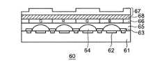
図5は、本発明による固体撮像素子のもう一つの実施例を示す部分断面図である。この実施例は、図2の構成において、半導体基板(11)と回折光学素子(16)の間にレンズを配置した実施例の部分断面図であり、固体撮像素子(60)は、表面に受光素子(62)、遮光膜(63)などが形成された半導体基板(61)上に、レンズ(64)、平坦化層(65)、カラーフィルター(66)、平坦化層(68)、回折光学素子(67)が順次形成されたものである。カラーフィルター(66)の下にはレンズ(64)が配置されており、回折光学素子(67)で集光された光を更に狭い範囲の領域に集光することができる。(Second Embodiment)
FIG. 5 is a partial cross-sectional view showing another embodiment of the solid-state imaging device according to the present invention. This embodiment is a partial cross-sectional view of an embodiment in which a lens is disposed between the semiconductor substrate (11) and the diffractive optical element (16) in the configuration of FIG. 2, and the solid-state imaging device (60) receives light on the surface. A lens (64), a flattening layer (65), a color filter (66), a flattening layer (68), diffractive optics on a semiconductor substrate (61) on which an element (62), a light shielding film (63), etc. are formed. Elements (67) are sequentially formed. A lens (64) is disposed under the color filter (66), and the light collected by the diffractive optical element (67) can be collected in a narrower region.
(第3実施形態)
図6は、本発明による固体撮像素子の更にもう一つの実施例を示す部分断面図である。この実施例は、図2の構成において、半導体基板(11)と回折光学素子(16)の間に更に回折光学素子を配置した実施例の部分断面図であり、固体撮像素子(70)は、表面に受光素子(72)、遮光膜(73)などが形成された半導体基板(71)上に、第1の回折光学素子(74)、平坦化層(75)、カラーフィルター(76)、平坦化層(78)、第2の回折光学素子(77)が順次形成されたものである。カラーフィルター(76)の下においては、白色光が既に赤色、青色、緑色に分かれているため、第1の回折光学素子(74)の高さは青色、赤色、緑色それぞれに対応して効率よく設計しても良い。また、回折光学素子(74)は周辺の平坦化層(75)より高屈折率のときに受光素子(72)に光がよく到達するものであり、光導波路的な効果も併せ持っている。(Third embodiment)
FIG. 6 is a partial sectional view showing still another embodiment of the solid-state imaging device according to the present invention. This embodiment is a partial cross-sectional view of an embodiment in which a diffractive optical element is further arranged between the semiconductor substrate (11) and the diffractive optical element (16) in the configuration of FIG. A first diffractive optical element (74), a planarization layer (75), a color filter (76), a flat surface on a semiconductor substrate (71) having a light receiving element (72), a light shielding film (73) and the like formed on the surface. Layer (78) and the second diffractive optical element (77) are sequentially formed. Under the color filter (76), since the white light is already divided into red, blue and green, the height of the first diffractive optical element (74) is efficiently corresponding to each of blue, red and green. You may design. In addition, the diffractive optical element (74) has a higher refractive index than the peripheral planarization layer (75), so that light reaches the light receiving element (72) well, and has an optical waveguide effect.
(第4実施形態)
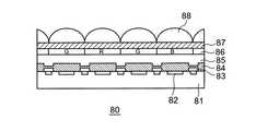
図7は、本発明による固体撮像素子の他の実施例を示す部分断面図である。この実施例は、図1に示した従来の固体撮像装置の構成において、マイクロレンズ(6)と半導体基板(1)の間に、回折光学素子を配置した構成であり、固体撮像素子(80)は、表面に受光素子(82)、遮光膜(83)などが形成された半導体基板(81)上に、回折光学素子(84)、平坦化層(85)、カラーフィルター(86)、平坦化層(87)、マイクロレンズ(88)が順次形成されたものである。この回折光学素子(84)は半導体基板(81)上に配置されるが、レンズ形成のような熱溶融による形成が不要であり、断面形状にレンズのような曲面が含まれず、レジストを用いて均一な厚さの層で構成されるため精度良く形成でき、この位置にマイクロレンズを作製するのが困難な場合には有効となる。また、回折光学素子(84)の屈折率が平坦化層(85)の屈折率より高い場合には非常に有効となり、光導波路的な意味合いでもある。(Fourth embodiment)
FIG. 7 is a partial sectional view showing another embodiment of the solid-state imaging device according to the present invention. This embodiment has a configuration in which a diffractive optical element is arranged between the microlens (6) and the semiconductor substrate (1) in the configuration of the conventional solid-state imaging device shown in FIG. 1, and the solid-state imaging device (80). Is a diffractive optical element (84), a planarization layer (85), a color filter (86), and a planarization on a semiconductor substrate (81) having a light receiving element (82), a light shielding film (83) and the like formed on the surface. A layer (87) and a microlens (88) are sequentially formed. Although this diffractive optical element (84) is disposed on the semiconductor substrate (81), it does not need to be formed by thermal melting as in lens formation, and the cross-sectional shape does not include a curved surface like a lens. Since it is composed of a layer having a uniform thickness, it can be formed with high precision, and is effective when it is difficult to produce a microlens at this position. Further, when the refractive index of the diffractive optical element (84) is higher than the refractive index of the flattening layer (85), it becomes very effective, and it also has an optical waveguide meaning.
次に、実施例及び比較例により本発明を更に詳述する。
図2に断面図を示した固体撮像素子について、電磁波による光強度のシュミレーションを米国R-Soft社のソフトBeamPROP(ver5.0)を用い、以下の設定にて行った。
Waveguide Model Dimension:2D
Vector Mode:Full
Polarization:TE
Simulation Tool:Beam PROP/BPM
Background Index:1
Profile Type:Step Index
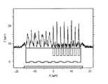
シュミレーション条件は、入射光の波長を緑色の中心波長である550nm、画素サイズ2.0μm、第1の平坦化層の屈折率1.5、厚さ3.8μm、カラーフィルターの屈折率1.6、厚さ1.0μm、第2の平坦化層の屈折率1.5、厚さ0.7μm、回折光学素子の屈折率1.6、幅2.0μm、高さを同一面内で0.1〜1.3μmに変化させ、回折光学素子下から受光面までの距離は5.5μmにて行い、このシュミレーション結果の光強度の断面(プロファイル)を図8に示した。この結果から、回折光学素子の高さが0.3μm〜0.8μm(0.65π〜1.74π)の範囲のとき入射光が受光素子面上にて良好に集光しており、回折光学素子の高さが0.5μm(1.09π)のとき最も集光度が上がっている。また、受光素子面の位置にも自由度がある(焦点深度が深い)ことも回折光学素子の利点である。Next, the present invention will be described in more detail with reference to examples and comparative examples.
With respect to the solid-state imaging device whose cross-sectional view is shown in FIG. 2, the simulation of light intensity by electromagnetic waves was performed using the software R-Soft software BeamPROP (ver5.0) with the following settings.
Waveguide Model Dimension: 2D
Vector Mode: Full
Polarization: TE
Simulation Tool: Beam PROP / BPM
Background Index: 1
Profile Type: Step Index
The simulation condition is that the wavelength of incident light is 550 nm, which is the center wavelength of green, the pixel size is 2.0 μm, the refractive index of the first planarization layer is 1.5, the thickness is 3.8 μm, and the refractive index of the color filter is 1.6. The thickness is 1.0 μm, the refractive index of the second planarization layer is 1.5, the thickness is 0.7 μm, the refractive index of the diffractive optical element is 1.6, the width is 2.0 μm, and the height is 0. The distance from the bottom of the diffractive optical element to the light receiving surface was changed to 5.5 μm, and the light intensity cross section (profile) of the simulation result is shown in FIG. From this result, when the height of the diffractive optical element is in the range of 0.3 μm to 0.8 μm (0.65π to 1.74π), incident light is well condensed on the surface of the light receiving element. When the height of the element is 0.5 μm (1.09π), the light condensing degree is the highest. Another advantage of the diffractive optical element is that the position of the light receiving element surface also has a degree of freedom (a deep focal depth).
次に、入射光の波長をそれぞれ赤色の中心波長の630nm、青色の中心波長の450nmに変えてシュミレーションを行った結果を図9,図10に示した。入射光が630nmのときには回折光学素子の高さが0.4μm〜0.8μm(0.76π〜1.52π)の範囲で受光素子面上にて良好に入射光が集光しており、入射光が450nmのときには回折光学素子の高さが0.3μm〜0.7μm(0.80π〜1.87π)の範囲で受光素子面上にて良好に入射光が集光している。よって、回折光学素子の高さを0.4μm〜0.7μm(緑色の中心波長550nmに対して0.87π〜1.52π)の範囲で設計すれば固体撮像素子として機能する。 Next, simulation results are shown in FIGS. 9 and 10 in which the wavelength of incident light is changed to the red center wavelength of 630 nm and the blue center wavelength of 450 nm, respectively. When the incident light is 630 nm, the incident light is well condensed on the light receiving element surface when the height of the diffractive optical element is in the range of 0.4 μm to 0.8 μm (0.76π to 1.52π). When the light is 450 nm, the incident light is well collected on the surface of the light receiving element when the height of the diffractive optical element is in the range of 0.3 μm to 0.7 μm (0.80π to 1.87π). Therefore, if the height of the diffractive optical element is designed in the range of 0.4 μm to 0.7 μm (0.87π to 1.52π with respect to the green central wavelength of 550 nm), it functions as a solid-state imaging device.
図5に断面図を示した固体撮像素子について、電磁波による光強度のシュミレーションを実施例1と同様のソフトを用いて、同様の設定にて行った。シュミレーション条件は、入射光の波長550nm、画素サイズ2.0μm、窒化シリコン(Si3N4)からなるレンズの屈折率2.0、高さ1.0μm、第1の平坦化層の屈折率1.5、厚さ3.8μm、カラーフィルターの屈折率1.6、厚さ1.0μm、第2の平坦化層の屈折率1.5、厚さ0.7μm、回折光学素子の屈折率1.6、幅2.0μm、高さ0.5μm、回折光学素子下から受光面までの距離は5.5μmにて行い、このシュミレーション結果の光強度の断面(プロファイル)を図11に示した。図11において、グラフの左半分は比較のため受光素子上にレンズを設けない場合の結果を示した。この結果から、受光素子上にレンズを配置すると、より入射光が集光することがわかる。With respect to the solid-state imaging device whose cross-sectional view is shown in FIG. The simulation conditions are: incident light wavelength 550 nm, pixel size 2.0 μm, refractive index 2.0 of lens made of silicon nitride (Si3 N4 ), height 1.0 μm,
図6に断面図を示した固体撮像素子について、電磁波による光強度のシュミレーションを実施例1と同様のソフトを用いて、同様の設定にて行った。シュミレーション条件は、入射光の波長550nm、画素サイズ2.0μm、窒化シリコン(Si3N4)からなる第1の回折光学素子の屈折率2.0、幅1.0μm、高さ5.9μm、第1の平坦化層の屈折率1.5、厚さ5.8μm、カラーフィルターの屈折率1.6、厚さ1.0μm、第2の平坦化層の屈折率1.5、厚さ0.7μm、第2の回折光学素子の屈折率1.6、幅2.0μm、高さ0.5μm、回折光学素子下から受光面までの距離は7.5μmにて行い、このシュミレーション結果の光強度の断面(プロファイル)を図12に示した。図12において、グラフの左半分は比較のため受光素子上に第1の回折光学素子を設けない場合の結果を示した。この結果から、受光素子上にも回折光学素子を配置すると、より入射光が集光することがわかる。For the solid-state imaging device whose cross-sectional view is shown in FIG. 6, the simulation of light intensity by electromagnetic waves was performed using the same software as in Example 1 with the same settings. The simulation conditions are: incident light wavelength 550 nm, pixel size 2.0 μm, refractive index 2.0 of first diffractive optical element made of silicon nitride (Si3 N4 ), width 1.0 μm, height 5.9 μm, The refractive index of the first planarization layer is 1.5, the thickness is 5.8 μm, the refractive index of the color filter is 1.6, the thickness is 1.0 μm, the refractive index of the second planarization layer is 1.5, and the thickness is 0. .7 μm, refractive index of the second diffractive optical element is 1.6, width is 2.0 μm, height is 0.5 μm, and the distance from the bottom of the diffractive optical element to the light receiving surface is 7.5 μm. A cross section (profile) of the strength is shown in FIG. In FIG. 12, the left half of the graph shows the result when the first diffractive optical element is not provided on the light receiving element for comparison. From this result, it can be seen that if the diffractive optical element is also arranged on the light receiving element, the incident light is more condensed.
図7に断面図を示した固体撮像素子について、電磁波による光強度のシュミレーションを実施例1と同様のソフトを用いて、同様の設定にて行った。シュミレーション条件は、入射光の波長550nm、画素サイズ2.0μm、窒化シリコン(Si3N4)からなる回折光学素子の屈折率2.0、幅0.9μm、高さ4.5μm、第1の平坦化層の屈折率1.5、厚さ4.8μm、カラーフィルターの屈折率1.6、厚さ1.0μm、第2の平坦化層の屈折率1.5、厚さ0.7μm、レンズの屈折率1.6、幅2.0μm、高さを同一面内で0.2〜0.9μmに変化させ、回折光学素子下から受光面までの距離は6.5μmにて行い、このシュミレーション結果の光強度の断面(プロファイル)を図13に示した。図13において、グラフの左半分は比較のため受光素子上に回折光学素子を設けない場合の結果を示した。この結果から、受光素子上に回折光学素子を配置するとより入射光が集光し、レンズの高さが0.6μmのとき最も集光度が上がっていることがわかる。For the solid-state imaging device whose cross-sectional view is shown in FIG. 7, the simulation of light intensity by electromagnetic waves was performed using the same software as in Example 1 with the same settings. The simulation conditions were as follows: incident light wavelength 550 nm, pixel size 2.0 μm, refractive index 2.0 of a diffractive optical element made of silicon nitride (Si3 N4 ), width 0.9 μm, height 4.5 μm, first The refractive index of the planarization layer is 1.5, the thickness is 4.8 μm, the refractive index of the color filter is 1.6, the thickness is 1.0 μm, the refractive index of the second planarization layer is 1.5, the thickness is 0.7 μm, The refractive index of the lens is 1.6, the width is 2.0 μm, and the height is changed from 0.2 to 0.9 μm in the same plane, and the distance from the bottom of the diffractive optical element to the light receiving surface is 6.5 μm. FIG. 13 shows a cross section (profile) of light intensity as a result of the simulation. In FIG. 13, the left half of the graph shows the result when no diffractive optical element is provided on the light receiving element for comparison. From this result, it can be seen that when the diffractive optical element is arranged on the light receiving element, the incident light is more condensed, and the degree of condensing is highest when the height of the lens is 0.6 μm.
〔比較例〕
図1に断面図を示した従来の固体撮像素子について、電磁波による光強度のシュミレーションを実施例1と同様のソフトを用いて、同様の設定にて行った。シュミレーション条件は、入射光の波長550nm、受光素子のサイズ2.0μm、第1の平坦化層の屈折率1.5、厚さ3.8μm、カラーフィルターの屈折率1.6、厚さ1.0μm、第2の平坦化層の屈折率1.5、厚さ0.7μm、レンズの屈折率1.6、幅2.0μm、高さを同一面内で0.1〜1.0μmに変化させ、レンズ下から受光面までの距離は5.5μmにて行い、このシュミレーション結果の光強度の断面(プロファイル)を図14に示した。この結果から、受光素子のピッチを2μm程度と光の波長に近づけた場合、レンズの曲率を下げて受光素子面で集光を得ようとしても、良好に集光できないことがわかる。[Comparative Example]
With respect to the conventional solid-state imaging device whose cross-sectional view is shown in FIG. The simulation conditions were as follows: incident light wavelength 550 nm, light receiving element size 2.0 μm, first planarization layer refractive index 1.5, thickness 3.8 μm, color filter refractive index 1.6,
本発明は、デジタルスチルカメラ、デジタルビデオカメラ、携帯電話に組み込まれるカメラ、防犯用監視カメラなどに用いられる固体撮像装置の製造に適用することができる。 The present invention can be applied to manufacture of a solid-state imaging device used for a digital still camera, a digital video camera, a camera incorporated in a mobile phone, a security surveillance camera, and the like.
1,11,61,71,81…半導体基板
2,12,62,72,82…受光素子
3,13,63,73,83…遮光膜
4,7,14,17,65,68,75,78,85,87…平坦化層
5,15,66,76,86…カラーフィルター
6,64,88…マイクロレンズ
10,60,70,80…固体撮像素子
16,67,74,77,84…回折光学素子
20,21…正方形領域
22…正方形領域の境界
30…物体光
32,33…回折光
34…境界線の近傍領域
35…正方形領域の中心領域
40…基板
41…正方形領域
42…境界線
43…周辺領域
44…中心領域
45…光量分布
1, 11, 61, 71, 81...
Claims (7)
Translated fromJapanesePriority Applications (1)
| Application Number | Priority Date | Filing Date | Title |
|---|---|---|---|
| JP2004197969AJP4784052B2 (en) | 2004-07-05 | 2004-07-05 | Solid-state image sensor |
Applications Claiming Priority (1)
| Application Number | Priority Date | Filing Date | Title |
|---|---|---|---|
| JP2004197969AJP4784052B2 (en) | 2004-07-05 | 2004-07-05 | Solid-state image sensor |
Publications (2)
| Publication Number | Publication Date |
|---|---|
| JP2006019627A JP2006019627A (en) | 2006-01-19 |
| JP4784052B2true JP4784052B2 (en) | 2011-09-28 |
Family
ID=35793581
Family Applications (1)
| Application Number | Title | Priority Date | Filing Date |
|---|---|---|---|
| JP2004197969AExpired - Fee RelatedJP4784052B2 (en) | 2004-07-05 | 2004-07-05 | Solid-state image sensor |
Country Status (1)
| Country | Link |
|---|---|
| JP (1) | JP4784052B2 (en) |
Families Citing this family (6)
| Publication number | Priority date | Publication date | Assignee | Title |
|---|---|---|---|---|
| JP5188107B2 (en) | 2007-06-21 | 2013-04-24 | 株式会社東芝 | Array type photo detector |
| JP5319370B2 (en)* | 2009-04-06 | 2013-10-16 | オリンパス株式会社 | Imaging device pixel structure structure determination method, imaging device pixel structure structure determination program, and imaging device pixel structure structure determination device |
| CN103364926A (en)* | 2013-07-15 | 2013-10-23 | 南昌欧菲光电技术有限公司 | Arrayed lens module |
| KR102391632B1 (en)* | 2016-06-07 | 2022-04-27 | 애어리3디 인크. | Light field imaging device and depth acquisition and three-dimensional imaging method |
| US12166053B2 (en) | 2021-03-11 | 2024-12-10 | Visera Technologies Company Limited | Semiconductor device for receiving and collecting inclined light |
| CN119343998A (en)* | 2022-07-19 | 2025-01-21 | 索尼半导体解决方案公司 | Solid-state imaging device |
Family Cites Families (5)
| Publication number | Priority date | Publication date | Assignee | Title |
|---|---|---|---|---|
| JPH05191733A (en)* | 1992-01-16 | 1993-07-30 | Hitachi Ltd | Solid-state image pickup device |
| JPH10163465A (en)* | 1996-12-05 | 1998-06-19 | Olympus Optical Co Ltd | Solid state image sensor and mutiplate image pickup unit therefor |
| US6665014B1 (en)* | 1998-11-25 | 2003-12-16 | Intel Corporation | Microlens and photodetector |
| JP2002243908A (en)* | 2001-02-13 | 2002-08-28 | Minolta Co Ltd | Optical element for ir ray and ir camera |
| JP5013660B2 (en)* | 2004-03-29 | 2012-08-29 | キヤノン株式会社 | Image sensor |
- 2004
- 2004-07-05JPJP2004197969Apatent/JP4784052B2/ennot_activeExpired - Fee Related
Also Published As
| Publication number | Publication date |
|---|---|
| JP2006019627A (en) | 2006-01-19 |
Similar Documents
| Publication | Publication Date | Title |
|---|---|---|
| US9853073B2 (en) | Image sensor for producing vivid colors and method of manufacturing the same | |
| US9099370B2 (en) | Solid-state imaging element and imaging device | |
| US11323608B2 (en) | Image sensors with phase detection auto-focus pixels | |
| US8004595B2 (en) | Solid-state imaging device with a two-dimensional array of unit pixels | |
| KR101265432B1 (en) | Imaging element and imaging apparatus using the same | |
| JP5188107B2 (en) | Array type photo detector | |
| US9425229B2 (en) | Solid-state imaging element, imaging device, and signal processing method including a dispersing element array and microlens array | |
| JP7574860B2 (en) | Image pickup element and image pickup device | |
| JP2008192771A (en) | Solid-state imaging device and manufacturing method thereof | |
| KR100628231B1 (en) | Image sensor having a square microlens and its manufacturing method | |
| JP2009266900A (en) | Solid-state image sensor | |
| KR20060006202A (en) | CMOS image sensor and its manufacturing method | |
| US8848092B2 (en) | Solid-state imaging device and electronic apparatus | |
| JP4784052B2 (en) | Solid-state image sensor | |
| EP4037299B1 (en) | Image capture element and image capture device | |
| JP7563472B2 (en) | Optical element, imaging element, and imaging device | |
| JP6801230B2 (en) | Solid-state image sensor and electronic equipment | |
| JP2007227474A (en) | Solid-state imaging device | |
| JP2009170562A (en) | Solid-state imaging device and method for manufacturing solid-state imaging device | |
| JP2009146957A (en) | Solid-state imaging device and method for manufacturing solid-state imaging device | |
| JP2006165162A (en) | Solid-state image sensor | |
| WO2013046531A1 (en) | Solid-state image pickup device | |
| TWI786668B (en) | Optical devices and method for fabricating the same | |
| JP2024084964A (en) | Solid-state imaging device and its manufacturing method | |
| JP2019204932A (en) | Solid-state imaging device |
Legal Events
| Date | Code | Title | Description |
|---|---|---|---|
| A621 | Written request for application examination | Free format text:JAPANESE INTERMEDIATE CODE: A621 Effective date:20070518 | |
| A977 | Report on retrieval | Free format text:JAPANESE INTERMEDIATE CODE: A971007 Effective date:20100416 | |
| A131 | Notification of reasons for refusal | Free format text:JAPANESE INTERMEDIATE CODE: A131 Effective date:20100506 | |
| A521 | Request for written amendment filed | Free format text:JAPANESE INTERMEDIATE CODE: A523 Effective date:20100608 | |
| TRDD | Decision of grant or rejection written | ||
| A01 | Written decision to grant a patent or to grant a registration (utility model) | Free format text:JAPANESE INTERMEDIATE CODE: A01 Effective date:20110614 | |
| A01 | Written decision to grant a patent or to grant a registration (utility model) | Free format text:JAPANESE INTERMEDIATE CODE: A01 | |
| A61 | First payment of annual fees (during grant procedure) | Free format text:JAPANESE INTERMEDIATE CODE: A61 Effective date:20110627 | |
| R150 | Certificate of patent or registration of utility model | Free format text:JAPANESE INTERMEDIATE CODE: R150 Ref document number:4784052 Country of ref document:JP Free format text:JAPANESE INTERMEDIATE CODE: R150 | |
| FPAY | Renewal fee payment (event date is renewal date of database) | Free format text:PAYMENT UNTIL: 20140722 Year of fee payment:3 | |
| LAPS | Cancellation because of no payment of annual fees |