JP4781648B2 - Optical resonator - Google Patents
Optical resonatorDownload PDFInfo
- Publication number
- JP4781648B2 JP4781648B2JP2004254814AJP2004254814AJP4781648B2JP 4781648 B2JP4781648 B2JP 4781648B2JP 2004254814 AJP2004254814 AJP 2004254814AJP 2004254814 AJP2004254814 AJP 2004254814AJP 4781648 B2JP4781648 B2JP 4781648B2
- Authority
- JP
- Japan
- Prior art keywords
- reflection film
- incident
- side reflection
- light
- optical waveguide
- Prior art date
- Legal status (The legal status is an assumption and is not a legal conclusion. Google has not performed a legal analysis and makes no representation as to the accuracy of the status listed.)
- Expired - Fee Related
Links
- 230000003287optical effectEffects0.000titleclaimsdescription280
- 239000000758substrateSubstances0.000claimsdescription120
- 239000013078crystalSubstances0.000claimsdescription50
- 239000000463materialSubstances0.000claimsdescription48
- 238000005498polishingMethods0.000claimsdescription35
- 230000005684electric fieldEffects0.000claimsdescription16
- 238000004519manufacturing processMethods0.000claimsdescription13
- 238000001514detection methodMethods0.000claimsdescription12
- 230000000694effectsEffects0.000claimsdescription12
- 230000010355oscillationEffects0.000claimsdescription12
- 230000003321amplificationEffects0.000claimsdescription11
- 238000000151depositionMethods0.000claimsdescription11
- 238000003199nucleic acid amplification methodMethods0.000claimsdescription11
- 238000010030laminatingMethods0.000claimsdescription5
- 230000003595spectral effectEffects0.000claimsdescription5
- 230000008021depositionEffects0.000claimsdescription4
- 238000009434installationMethods0.000claims1
- 238000003475laminationMethods0.000claims1
- 239000010408filmSubstances0.000description190
- 230000001681protective effectEffects0.000description46
- 238000004891communicationMethods0.000description24
- 229910013641LiNbO 3Inorganic materials0.000description18
- 230000001902propagating effectEffects0.000description16
- 238000000034methodMethods0.000description14
- 239000013307optical fiberSubstances0.000description9
- 238000010295mobile communicationMethods0.000description7
- 238000012545processingMethods0.000description7
- 230000005540biological transmissionEffects0.000description6
- 230000001360synchronised effectEffects0.000description6
- 230000008569processEffects0.000description5
- 238000002310reflectometryMethods0.000description5
- 229910004298SiO 2Inorganic materials0.000description4
- 230000007423decreaseEffects0.000description4
- 229920002120photoresistant polymerPolymers0.000description4
- 230000008901benefitEffects0.000description3
- 238000006243chemical reactionMethods0.000description3
- 230000005284excitationEffects0.000description3
- 229910001218Gallium arsenideInorganic materials0.000description2
- WPYMKLBDIGXBTP-UHFFFAOYSA-Nbenzoic acidChemical compoundOC(=O)C1=CC=CC=C1WPYMKLBDIGXBTP-UHFFFAOYSA-N0.000description2
- 239000011248coating agentSubstances0.000description2
- 238000000576coating methodMethods0.000description2
- 230000008878couplingEffects0.000description2
- 238000010168coupling processMethods0.000description2
- 238000005859coupling reactionMethods0.000description2
- 238000005520cutting processMethods0.000description2
- 238000009826distributionMethods0.000description2
- 238000005259measurementMethods0.000description2
- 239000007769metal materialSubstances0.000description2
- 229910052697platinumInorganic materials0.000description2
- 239000000126substanceSubstances0.000description2
- 238000002834transmittanceMethods0.000description2
- 239000005711Benzoic acidSubstances0.000description1
- 229910052691ErbiumInorganic materials0.000description1
- 230000005374Kerr effectEffects0.000description1
- 230000005697Pockels effectEffects0.000description1
- 238000010521absorption reactionMethods0.000description1
- 239000000853adhesiveSubstances0.000description1
- 229910052782aluminiumInorganic materials0.000description1
- 230000035559beat frequencyEffects0.000description1
- 238000005452bendingMethods0.000description1
- 235000010233benzoic acidNutrition0.000description1
- 230000002457bidirectional effectEffects0.000description1
- 230000015572biosynthetic processEffects0.000description1
- 238000004364calculation methodMethods0.000description1
- 210000001520combAnatomy0.000description1
- 229910052802copperInorganic materials0.000description1
- 238000011161developmentMethods0.000description1
- 238000005516engineering processMethods0.000description1
- -1erbium ionChemical class0.000description1
- 238000010438heat treatmentMethods0.000description1
- 230000003993interactionEffects0.000description1
- 239000012528membraneSubstances0.000description1
- 230000009022nonlinear effectEffects0.000description1
- 230000005693optoelectronicsEffects0.000description1
- 230000010287polarizationEffects0.000description1
- 230000000644propagated effectEffects0.000description1
- 230000035945sensitivityEffects0.000description1
- 238000004088simulationMethods0.000description1
- 238000001228spectrumMethods0.000description1
- 230000002269spontaneous effectEffects0.000description1
- 239000010409thin filmSubstances0.000description1
- 230000009466transformationEffects0.000description1
- 230000007704transitionEffects0.000description1
Images


Classifications
- G—PHYSICS
- G02—OPTICS
- G02F—OPTICAL DEVICES OR ARRANGEMENTS FOR THE CONTROL OF LIGHT BY MODIFICATION OF THE OPTICAL PROPERTIES OF THE MEDIA OF THE ELEMENTS INVOLVED THEREIN; NON-LINEAR OPTICS; FREQUENCY-CHANGING OF LIGHT; OPTICAL LOGIC ELEMENTS; OPTICAL ANALOGUE/DIGITAL CONVERTERS
- G02F2/00—Demodulating light; Transferring the modulation of modulated light; Frequency-changing of light
- G02F2/02—Frequency-changing of light, e.g. by quantum counters
- G—PHYSICS
- G02—OPTICS
- G02F—OPTICAL DEVICES OR ARRANGEMENTS FOR THE CONTROL OF LIGHT BY MODIFICATION OF THE OPTICAL PROPERTIES OF THE MEDIA OF THE ELEMENTS INVOLVED THEREIN; NON-LINEAR OPTICS; FREQUENCY-CHANGING OF LIGHT; OPTICAL LOGIC ELEMENTS; OPTICAL ANALOGUE/DIGITAL CONVERTERS
- G02F1/00—Devices or arrangements for the control of the intensity, colour, phase, polarisation or direction of light arriving from an independent light source, e.g. switching, gating or modulating; Non-linear optics
- G02F1/01—Devices or arrangements for the control of the intensity, colour, phase, polarisation or direction of light arriving from an independent light source, e.g. switching, gating or modulating; Non-linear optics for the control of the intensity, phase, polarisation or colour
- G02F1/21—Devices or arrangements for the control of the intensity, colour, phase, polarisation or direction of light arriving from an independent light source, e.g. switching, gating or modulating; Non-linear optics for the control of the intensity, phase, polarisation or colour by interference
- G02F1/225—Devices or arrangements for the control of the intensity, colour, phase, polarisation or direction of light arriving from an independent light source, e.g. switching, gating or modulating; Non-linear optics for the control of the intensity, phase, polarisation or colour by interference in an optical waveguide structure
- G—PHYSICS
- G02—OPTICS
- G02F—OPTICAL DEVICES OR ARRANGEMENTS FOR THE CONTROL OF LIGHT BY MODIFICATION OF THE OPTICAL PROPERTIES OF THE MEDIA OF THE ELEMENTS INVOLVED THEREIN; NON-LINEAR OPTICS; FREQUENCY-CHANGING OF LIGHT; OPTICAL LOGIC ELEMENTS; OPTICAL ANALOGUE/DIGITAL CONVERTERS
- G02F2203/00—Function characteristic
- G02F2203/56—Frequency comb synthesizer
- H—ELECTRICITY
- H01—ELECTRIC ELEMENTS
- H01S—DEVICES USING THE PROCESS OF LIGHT AMPLIFICATION BY STIMULATED EMISSION OF RADIATION [LASER] TO AMPLIFY OR GENERATE LIGHT; DEVICES USING STIMULATED EMISSION OF ELECTROMAGNETIC RADIATION IN WAVE RANGES OTHER THAN OPTICAL
- H01S3/00—Lasers, i.e. devices using stimulated emission of electromagnetic radiation in the infrared, visible or ultraviolet wave range
- H01S3/05—Construction or shape of optical resonators; Accommodation of active medium therein; Shape of active medium
- H01S3/06—Construction or shape of active medium
- H01S3/063—Waveguide lasers, i.e. whereby the dimensions of the waveguide are of the order of the light wavelength
- H01S3/0632—Thin film lasers in which light propagates in the plane of the thin film
- H01S3/0637—Integrated lateral waveguide, e.g. the active waveguide is integrated on a substrate made by Si on insulator technology (Si/SiO2)
- H—ELECTRICITY
- H01—ELECTRIC ELEMENTS
- H01S—DEVICES USING THE PROCESS OF LIGHT AMPLIFICATION BY STIMULATED EMISSION OF RADIATION [LASER] TO AMPLIFY OR GENERATE LIGHT; DEVICES USING STIMULATED EMISSION OF ELECTROMAGNETIC RADIATION IN WAVE RANGES OTHER THAN OPTICAL
- H01S3/00—Lasers, i.e. devices using stimulated emission of electromagnetic radiation in the infrared, visible or ultraviolet wave range
- H01S3/14—Lasers, i.e. devices using stimulated emission of electromagnetic radiation in the infrared, visible or ultraviolet wave range characterised by the material used as the active medium
- H01S3/16—Solid materials
- H01S3/1601—Solid materials characterised by an active (lasing) ion
- H01S3/1603—Solid materials characterised by an active (lasing) ion rare earth
- H01S3/1608—Solid materials characterised by an active (lasing) ion rare earth erbium
- H—ELECTRICITY
- H01—ELECTRIC ELEMENTS
- H01S—DEVICES USING THE PROCESS OF LIGHT AMPLIFICATION BY STIMULATED EMISSION OF RADIATION [LASER] TO AMPLIFY OR GENERATE LIGHT; DEVICES USING STIMULATED EMISSION OF ELECTROMAGNETIC RADIATION IN WAVE RANGES OTHER THAN OPTICAL
- H01S3/00—Lasers, i.e. devices using stimulated emission of electromagnetic radiation in the infrared, visible or ultraviolet wave range
- H01S3/23—Arrangements of two or more lasers not provided for in groups H01S3/02 - H01S3/22, e.g. tandem arrangements of separate active media
- H01S3/2308—Amplifier arrangements, e.g. MOPA
Landscapes
- Physics & Mathematics (AREA)
- Nonlinear Science (AREA)
- General Physics & Mathematics (AREA)
- Optics & Photonics (AREA)
- Optical Modulation, Optical Deflection, Nonlinear Optics, Optical Demodulation, Optical Logic Elements (AREA)
- Optical Integrated Circuits (AREA)
- Lasers (AREA)
Description
Translated fromJapanese本発明は、光通信、光CT、光周波数標準器など多波長でコヒーレンス性の高い標準光源、又は、各波長間のコヒーレンス性も利用できる光源を必要とする分野に適用される光共振器、光変調器、光周波数コム発生器、光発振器、並びにその光共振器の作製方法に関する。 The present invention is an optical resonator applied to a field that requires a standard light source having high coherence at multiple wavelengths, such as optical communication, optical CT, or an optical frequency standard, or a light source that can also utilize coherence between wavelengths, The present invention relates to an optical modulator, an optical frequency comb generator, an optical oscillator, and a method for manufacturing the optical resonator.
光周波数を高精度に測定する場合には、測定する光を他の光と干渉させ、発生する光ビート周波数の電気信号を検出するヘテロダイン検波を行う。このヘテロダイン検波において測定可能な光の帯域は、検波系に使用される受光素子の帯域に制限され、概ね数十GHz程度である。 In the case of measuring the optical frequency with high accuracy, heterodyne detection is performed in which the light to be measured is made to interfere with other light and an electric signal having a generated optical beat frequency is detected. The band of light that can be measured in this heterodyne detection is limited to the band of the light receiving element used in the detection system, and is about several tens of GHz.
一方、近年の光エレクトロニクスの発展に伴い、周波数多重通信のための光制御や、広範囲に分布する吸収線の周波数測定を行うため、光の測定可能帯域を更に拡大する必要がある。 On the other hand, with the recent development of optoelectronics, it is necessary to further expand the measurable band of light in order to perform optical control for frequency division multiplexing and frequency measurement of absorption lines distributed over a wide range.
かかる測定可能帯域の拡大化の要請に応えるべく、従来において光周波数コム発生器(例えば、特許文献1参照。)を用いた広帯域なヘテロダイン検波系が提案されている。この光周波数コム発生器は、周波数軸上で等間隔に配置された櫛状のサイドバンドを広帯域にわたり発生させるものであり、このサイドバンドの周波数安定度は、入射光の周波数安定度とほぼ同等である。この生成したサイドバンドと被測定光をヘテロダイン検波することにより、数THzに亘る広帯域なヘテロダイン検波系を構築することが可能となる。 In order to meet the demand for an increase in the measurable bandwidth, a wideband heterodyne detection system using an optical frequency comb generator (see, for example, Patent Document 1) has been proposed. This optical frequency comb generator generates comb-like sidebands arranged at equal intervals on the frequency axis over a wide band, and the frequency stability of this sideband is almost equal to the frequency stability of incident light. It is. By heterodyne detection of the generated sideband and light to be measured, a wideband heterodyne detection system over several THz can be constructed.
図15は、この従来における光周波数コム発生器3の原理的な構造を示している。 FIG. 15 shows the basic structure of the conventional optical
この光周波数コム発生器3は、光位相変調器31と、この光位相変調器31を介して互いに対向するように設置された反射鏡32,33を備える光共振器100が使用されている。 The optical
この光共振器100は、反射鏡32を介して僅かな透過率で入射した光Linを、反射鏡32,33間で共振させ、その一部の光Loutを反射鏡33を介して出射させる。光位相変調器31は、電界を印加することにより屈折率が変化する光位相変調のための電気光学結晶からなり、この光共振器100を通過する光に対して、電極36に印加される周波数fmの電気信号に応じて位相変調をかける。The
この光周波数コム発生器3において、光が光共振器100内を往復する時間に同期した電気信号を電極36から光位相変調器31へ駆動入力することにより、光位相変調器31を1回だけ通過する場合に比べ、数十倍以上の深い位相変調をかけることが可能となる。これにより、高次のサイドバンドを数百本生成することができ、隣接したサイドバンドの周波数間隔fm は全て入力された電気信号の周波数fmと同等になる。 In this optical
また、従来における光周波数コム発生器は、上述のバルク型に限定されるものではない。例えば図16に示すように、導波路を用いた導波路型光周波数コム発生器200にも適用可能である。 Further, the conventional optical frequency comb generator is not limited to the above-described bulk type. For example, as shown in FIG. 16, the present invention can also be applied to a waveguide type optical
この導波路型光周波数コム発生器20は、導波路型光変調器200から構成される。導波路型光変調器200は、基板201と、導波路202と、電極203と、入射側反射膜204と、出射側反射膜205と、発振器206とを備える。 The waveguide type optical
基板201は、例えば引き上げ法により育成された3〜4インチ径のLiNbO3やGaAs等の大型結晶をウェハ状に切り出したものである。この切り出した基板201上には、機械研磨や化学研磨等の処理を施す。The
導波路202は、光を伝搬させるために配されたものであり、導波路202を構成する層の屈折率は、基板201等の他層よりも高く設定されている。導波路202に入射した光は、導波路202の境界面で全反射しながら伝搬する。一般に、この導波路202は、基板201中においてTi原子を拡散させることにより、或いは基板201上へのエピタキシャル成長させることにより作製することができる。 The
なお、この導波路202として、LiNbO3結晶光導波路を適用してもよい。このLiNbO3結晶光導波路は、LiNbO3等からなる基板201表面にTiを拡散させることにより形成することができる。このLiNbO3結晶光導波路を実際に作製する場合には、先ずこの基板201の表面にフォトレジストのパターンを作製し、そこにTiを蒸着させ、さらにこのフォトレジストを除去することにより、ミクロンサイズの幅で構成されるTiの細線を作製する。次に、このTiの細線を加熱することにより、これを基板201中に熱拡散させる。As the
ちなみに、このTiがLiNbO3からなる基板201中に熱拡散されると、かかるTiが拡散された領域については他の領域よりも屈折率が高くなるところ、光を閉じ込めることができることになる。即ち、かかるTiが拡散された領域につき光を伝搬させることができる導波路202が形成されることになる。このような方法に基づいて作製したLiNbO3結晶型の導波路202は電気光学効果を有するため、これに対して電界を印加することにより屈折率を変化させることができる。Incidentally, when this Ti is thermally diffused into the
電極203は、例えばAlやCu、Pt、Au等の金属材料からなり、外部から供給された周波数fmの電気信号を導波路202に駆動入力する。また、導波路202における光の伝搬方向と変調電界の進行方向は同一となる。この電極203の幅や厚さを調整することにより、導波路202を伝搬する光の速度と電極203上を伝搬する電気信号の速度を一致させるようにしてもよい。これにより、導波路202を伝搬する光が感じる電気信号の位相を一定に保つことが可能となる。 The
入射側反射膜204及び出射側反射膜205は、導波路202に入射した光を共振させるため設けられたものであり、導波路202を通過する光を往復反射させることにより共振させる。発振器206は、電極203に接続され、周波数fmの電気信号を供給する。 The incident-
入射側反射膜204は、導波路型光変調器200の光入射側に配され、図示しない光源から周波数ν1の光が入射される。また、この入射側反射膜204は、出射側反射膜205により反射されて、かつ導波路202を通過した光を反射する。The incident-
出射側反射膜205は、導波路型光変調器200の光出射側に配され、導波路202を通過した光を反射する。またこの出射側反射膜205は、導波路202を通過した光を一定の割合で外部に出射する。 The exit-
上述の構成からなる導波路型光周波数コム発生器20において、光が導波路202内を往復する時間に同期した電気信号を電極203から導波路型光変調器200へ駆動入力とすることにより、光位相変調器111を1回だけ通過する場合に比べ、数十倍以上の深い位相変調をかけることが可能となる。これにより、バルク型光周波数コム発生器10と同様に、広帯域にわたるサイドバンドを有する光周波数コムを生成することができ、隣接したサイドバンドの周波数間隔は、全て入力された電気信号の周波数fmと同等になる。 In the waveguide-type optical
この導波路型光周波数コム発生器20の特徴は、光と電気信号の相互作用領域がより小さいことにある。光は周囲より屈折率が高いミクロンオーダの導波路202に閉じ込められて伝搬することになるため、導波路202の極近傍に電極203を取り付けることにより、導波路202中の電界強度を局所的に高めることが可能となる。従って、バルク型の光周波数コム発生器3と比較して導波路202に生じる電気光学効果が大きくなり、少ない電力で大きな変調を得ることが可能となる。 The waveguide type optical
しかしながら、上述した従来の導波路型光周波数コム発生器20は、導波路202の構造上、入射側反射膜204及び出射側反射膜205の被着並びにこれらが被着される端面の研磨が困難であり、高いフィネスの共振器を再現性良く作ることが難しかった。導波路型光周波数コム発生器20の性能を高めるためには、これら入射側反射膜204及び出射側反射膜205で構成される共振器のフィネスを高めることが不可欠となる。導波路202における往路方向又は復路方向のみの変調指数が高くても、フィネスそのものが低い場合には、光の往復回数を増加させることができないため、広帯域に亘り高強度のサイドバンドを発生させることができないからである。 However, in the conventional waveguide-type optical
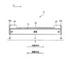
また図17は、導波路型光周波数コム発生器20における、入射側反射膜204が形成されている端面を示している。この図17によれば、基板201の上端に導波路202が形成され、その上に薄いバッファ層が積層されてなり、その上において更に電極203が形成されている。即ち、この導波路202は、導波路型光周波数コム発生器20の端面最上部の角に位置している。この端面最上部の角は、尖っているため研磨時に図17に示すように欠けが生じてしまう場合が多い。端面最上部に欠けが生じると、共振すべき光が散乱されて損失となる。 FIG. 17 shows an end face of the waveguide type optical
また、端面研磨の状態によっては、端面最上部における角の欠けに至らなくても、角が丸くなる場合がある。角が丸くなると反射された光の一部が導波路202の導波モードから外れ、損失となる。 Further, depending on the state of the end face polishing, the corner may be rounded even if the corner at the uppermost end face is not chipped. When the corner is rounded, a part of the reflected light deviates from the waveguide mode of the
また、ごく稀に端面最上部における角の欠けが発生せず、また角が丸くならない状態で研磨することができる場合もあるが、かかる場合においても、端面に入射側反射膜204を形成させる際に問題が発生する。入射側反射膜204等の高反射膜は、通常、屈折率の高い膜と低い膜を交互に堆積することによって作製されるが、端面最上部における角の部分は、膜そのものが剥がれやすく、また高反射膜の材料が端面から側面へ回り込むことにより膜厚が変化する結果、設計通りの膜厚に制御することができないという問題点もある。 In addition, in some rare cases, corners are not chipped at the uppermost portion of the end face, and polishing can be performed in a state where the corners are not rounded. However, even in such a case, when the incident-side
即ち、従来の導波路型光周波数コム発生器20における問題点をまとめると、以下のとおりになる。 That is, the problems in the conventional waveguide type optical
先ず、導波路202の端面が上述の如き端面最上部の角に位置することから、1)導波路202の端面の角が加工時に欠けやすい、2)導波路202の端面の角が加工時に丸くなることがある、3)導波路202の端面に形成された反射膜が、端面最上部の角の部分で剥がれやすくなる、4)導波路202の端面に形成された反射膜が、端面最上部の角の部分から回り込む結果、設計通りの膜厚に制御することができない、という問題点があった。 First, since the end face of the
これらの問題は、導波路202の端面に被着される反射膜の反射率低下、入射側反射膜204及び出射側反射膜205で構成される共振器のフィネス低下、導波路型光周波数コム発生器20自身の機能の低下等を招く。 These problems include a decrease in reflectivity of the reflection film deposited on the end face of the
更に、これら1)〜4)の問題点は、作製環境に依存するため、導波路型光周波数コム発生器20や、これを適用した導波路型のファブリペロー共振器の性能における再現性を担保することができず、歩留まりを向上させることができなかった。 Further, since the problems 1) to 4) depend on the production environment, the reproducibility in the performance of the waveguide type optical
そこで、本発明は、上述した問題点に鑑みて案出されたものであり、その目的とするところは、導波路端面の角の加工時における欠けや丸まりを抑え、各反射膜につき端面最上部の角の部分で剥がれることなく安定して被着させることにより、反射膜の反射率や共振器のフィネスを向上させ、デバイスそのものの機能を高めた光共振器、光変調器、光周波数コム発生器、光発振器を提供することにあり、またかかる機能を有する光共振器の作製方法を提供することにある。 Therefore, the present invention has been devised in view of the above-described problems, and the object of the present invention is to suppress chipping and rounding during processing of the corners of the waveguide end face, and to provide the uppermost end face for each reflective film. Optical resonators, optical modulators, and optical frequency combs that improve the function of the device itself by improving the reflectivity of the reflective film and the finesse of the resonator by stably depositing without peeling off at the corners It is to provide an optical resonator and an optical oscillator, and to provide a method for manufacturing an optical resonator having such a function.
本発明に係る光共振器は、上述した問題点を解決するために、互いに平行な入射側反射膜及び出射側反射膜より構成され、入射側反射膜を介して入射された光を共振させる共振手段と、上記入射側反射膜から上記出射側反射膜にかけて貫通するように形成され、上記共振手段により共振された光を伝搬させる光導波路と、上記光導波路を上面から形成させるための基板と、上記基板と同じ硬さを持つ部材から構成され、上記部材における少なくとも一の端面が上記光導波路における光入射端又は光出射端を含む上記基板の端面と同一の平面を形成するように上記光導波路の上部に配設される端面保護手段とを備え、上記入射側反射膜並びに上記出射側反射膜は、上記部材の端面と上記基板の端面を研磨することにより形成される平面にそれぞれ被着されてなる。In order to solve the above-described problems, the optical resonator according to the present invention is configured by an incident-side reflection film and an emission-side reflection film that are parallel to each other, and resonates light incident through the incident-side reflection film. Means, an optical waveguide formed so as to penetrate from the incident side reflection film to the emission side reflection film, and propagates the light resonated by the resonance means, and a substrate for forming the optical waveguide from the upper surface, The optical waveguide is composed of a member having thesame hardness as the substrate,and at least one end surface of the member forms the same plane as the end surface of the substrate including a light incident end or a light emitting end of the optical waveguide. End surface protection means disposed on the upper surface of the substrate, and the incident side reflection film and the emission side reflection film are respectively formed in a plane formed by polishing the end surface of the member and the end surface of the substrate. Formed by deposition.
本発明に係る光変調器は、上述した問題点を解決するために、所定の周波数の変調信号を発振する発振手段と、互いに平行な入射側反射膜及び出射側反射膜より構成され、入射側反射膜を介して入射された光を共振させる共振手段と、上記入射側反射膜から上記出射側反射膜にかけて貫通するように形成され、上記発振手段から供給された上記変調信号に応じて上記共振手段により共振された光の位相を変調する光導波路と、上記光導波路を上面から形成させるための基板と、上記基板と同じ硬さを持つ部材から構成され、上記部材における少なくとも一の端面が上記光導波路における光入射端又は光出射端を含む上記基板の端面と同一の平面を形成するように上記光導波路の上部に配設される端面保護手段とを備え、上記入射側反射膜並びに上記出射側反射膜は、上記部材の端面と上記基板の端面を研磨することにより形成される平面にそれぞれ被着されてなる。In order to solve the above-described problems, an optical modulator according to the present invention includes an oscillating unit that oscillates a modulation signal having a predetermined frequency, and an incident-side reflecting film and an emitting-side reflecting film that are parallel to each other. Resonance means for resonating light incident through the reflective film, and formed so as to penetrate from the incident-side reflective film to the output-side reflective film, and in accordance with the modulation signal supplied from the oscillation means An optical waveguide that modulates the phase of the light resonated by the means, a substrate for forming the optical waveguide from the upper surface, and a member having thesame hardness as the substrate, wherein at least one end surface of the member is the above End face protection means disposed on the top of the optical waveguide so as to form the same plane as the end face of the substrate including the light incident end or light exit end in the optical waveguide, Said emission side reflecting film is formed by respectively deposited on the plane formed by polishing the end face and the end face of said substrate of said member.
本発明に係る光変調器は、上述した問題点を解決するために、電気信号を検出するための検出手段と、互いに平行な入射側反射膜及び出射側反射膜より構成され、入射側反射膜を介して入射された光を共振させる共振手段と、上記入射側反射膜から上記出射側反射膜にかけて貫通するように形成され、上記検出手段により検出された電気信号の波長に応じて上記共振手段により共振された光の位相を変調する光導波路と、上記光導波路を上面から形成させるための基板と、上記基板と同じ硬さを持つ部材から構成され、上記部材における少なくとも一の端面が上記光導波路における光入射端又は光出射端を含む上記基板の端面と同一の平面を形成するように上記光導波路の上部に配設される端面保護手段とを備え、上記入射側反射膜並びに上記出射側反射膜は、上記部材の端面と上記基板の端面を研磨することにより形成される平面にそれぞれ被着されてなる。In order to solve the above-described problems, an optical modulator according to the present invention includes a detecting means for detecting an electrical signal, and an incident-side reflecting film and an emitting-side reflecting film that are parallel to each other. Resonance means for resonating light incident through the light source, and the resonance means formed so as to penetrate from the incident-side reflection film to the emission-side reflection film according to the wavelength of the electrical signal detected by the detection means An optical waveguide that modulates the phase of the light resonated by the substrate, a substrate for forming the optical waveguide from the upper surface, and a member having thesame hardness as the substrate, wherein at least one end surface of the member is the optical waveguide End face protecting means disposed on the top of the optical waveguide so as to form the same plane as the end face of the substrate including the light incident end or light exit end in the waveguide, Emission side reflecting film is formed by depositing respective plane formed by polishing the end face and the end face of said substrate of said member.
本発明に係る光周波数コム発生器は、上述した問題点を解決するために、所定の周波数の変調信号を発振する発振手段と、互いに平行な入射側反射膜及び出射側反射膜より構成され、入射側反射膜を介して入射された光を共振させる共振手段と、上記入射側反射膜から上記出射側反射膜にかけて貫通するように形成され、上記発振手段から供給された上記変調信号に応じて上記共振手段により共振された光の位相を変調し、上記入射された光の周波数を中心としたサイドバンドを上記変調信号の周波数の間隔で生成する光導波路と、上記光導波路を上面から形成させるための基板と、上記基板と同じ硬さを持つ部材から構成され、上記部材における少なくとも一の端面が上記光導波路における光入射端又は光出射端を含む上記基板の端面と同一の平面を形成するように上記光導波路の上部に配設される端面保護手段とを備え、上記入射側反射膜並びに上記出射側反射膜は、上記部材の端面と上記基板の端面を研磨することにより形成される平面にそれぞれ被着されてなる。An optical frequency comb generator according to the present invention includes an oscillating unit that oscillates a modulation signal having a predetermined frequency, and an incident-side reflection film and an emission-side reflection film that are parallel to each other, in order to solve the above-described problems. Resonance means for resonating light incident through the incident-side reflection film, and formed so as to penetrate from the incident-side reflection film to the emission-side reflection film, and according to the modulation signal supplied from the oscillation means An optical waveguide that modulates the phase of the light resonated by the resonance means and generates a sideband centered on the frequency of the incident light at intervals of the frequency of the modulation signal, and the optical waveguide are formed from the top surface a substrate for, is composed of a member having thesame hardnessas the substrate, at least one end face is the same and the end face of the substrate including the light incident end or the light outgoing end of the optical waveguide in the member End face protection means disposed on the optical waveguide so as to form a flat surface of the optical waveguide, and the incident side reflection film and the emission side reflection film polish the end face of the member and the end face of the substrate. Are respectively attached to the plane formed by
本発明を適用した光発振器は、上述した問題点を解決するために、互いに平行な入射側反射膜及び出射側反射膜より構成され、入射側反射膜を介して入射された光、又はレーザ増幅により発生された光を共振させる共振手段と、上記入射側反射膜から上記出射側反射膜にかけて貫通するように形成され、上記共振手段により共振された光を増幅させるとともに、これを出射側反射膜を介して外部へ出射させる光導波路と、上記光導波路を上面から形成させるための基板と、上記基板と同じ硬さを持つ部材から構成され、上記部材における少なくとも一の端面が上記光導波路における光入射端又は光出射端を含む上記基板の端面と同一の平面を形成するように上記光導波路の上部に配設される端面保護手段とを備え、上記入射側反射膜並びに上記出射側反射膜は、上記部材の端面と上記基板の端面を研磨することにより形成される平面にそれぞれ被着されてなる。In order to solve the above-described problems, an optical oscillator to which the present invention is applied includes an incident-side reflecting film and an emitting-side reflecting film that are parallel to each other, and light incident through the incident-side reflecting film or laser amplification. Resonating means for resonating the light generated by the light source, and formed so as to penetrate from the incident side reflection film to the emission side reflection film, amplify the light resonated by the resonance means, An optical waveguide that emits light to the outside through the substrate, a substrate for forming the optical waveguide from the upper surface, and a member having thesame hardness as the substrate,and at least one end surface of the member is light in the optical waveguide End face protecting means disposed on the top of the optical waveguide so as to form the same plane as the end face of the substrate including the incident end or the light emitting end, and the incident side reflective film and the upper surface Emission side reflecting film is formed by depositing respective plane formed by polishing the end face and the end face of said substrate of said member.
本発明を適用した光発振器は、所定の周波数の変調信号を発振する発振手段と、互いに平行な入射側反射膜及び出射側反射膜より構成され、入射側反射膜を介して入射された光、又はレーザ増幅により発生された光を共振させる共振手段と、上記入射側反射膜から上記出射側反射膜にかけて貫通するように形成され、上記発振手段から供給された上記変調信号に応じて上記共振手段により共振された光を増幅させるとともに、これを出射側反射膜を介して外部へ出射させる光導波路と、上記光導波路を上面から形成させるための基板と、上記基板と同じ硬さを持つ部材から構成され、上記部材における少なくとも一の端面が上記光導波路における光入射端又は光出射端を含む上記基板の端面と同一の平面を形成するように上記光導波路の上部に配設される端面保護手段とを備え、上記入射側反射膜並びに上記出射側反射膜は、上記部材の端面と上記基板の端面を研磨することにより形成される平面にそれぞれ被着されてなり、レーザ発振する多モード間の位相同期をとる。An optical oscillator to which the present invention is applied is composed of an oscillation means that oscillates a modulation signal of a predetermined frequency, and an incident-side reflection film and an emission-side reflection film that are parallel to each other. Or resonance means for resonating light generated by laser amplification, and the resonance means formed so as to penetrate from the incident-side reflection film to the emission-side reflection film and according to the modulation signal supplied from the oscillation means From the optical waveguide that amplifies the light resonated by the optical fiber and emits the light to the outside through the output-side reflection film, the substrate for forming the optical waveguide from the upper surface, and a member having thesame hardness as the substrate The upper portion of the optical waveguide is configured such that at least one end surface of the member forms a plane that is the same as the end surface of the substrate including the light incident end or the light emitting end of the optical waveguide. The incident-side reflection film and the emission-side reflection film are respectively attached to a plane formed by polishing the end surface of the member and the end surface of the substrate. Phase synchronization between multiple modes that oscillate lasers is achieved.
また、この光発振器における光導波路は、自身の電気光学効果に基づいて、レーザ発振する多モード間の位相同期をとり、発振手段は、上記共振手段のFSR(Free Spectral Range)の整数倍の周波数からなる変調信号を発振する。 The optical waveguide in this optical oscillator obtains phase synchronization between multiple modes that oscillate lasers based on its electro-optic effect, and the oscillation means has a frequency that is an integral multiple of the FSR (Free Spectral Range) of the resonance means. A modulation signal consisting of
本発明を適用した光共振器の作製方法は、上述した問題点を解決するために、互いに平行な入射側反射膜及び出射側反射膜を貫通するように形成された光導波路により、互いに平行な入射側反射膜及び出射側反射膜を貫通するように形成された光導波路により、上記入射側反射膜を介して入射された光を共振させる光共振器の作製方法において、上記光導波路を基板の上面から形成する光導波路形成工程と、少なくとも上記光導波路形成工程において形成した光導波路を被覆するように上記基板上にバッファ層を積層する積層工程と、上記光導波路に対して電界を印加するための電極を上記積層工程において積層したバッファ層上に形成する電極形成工程と、上記基板と同じ硬さを持つ部材を、少なくともその一の端面が上記光導波路における光入射端又は光出射端を含む上記基板の端面と同一の平面を形成するように上記光導波路の上部に配設する配設工程と、上記配設工程において配置した上記部材の端面と上記基板の端面を研磨することにより平面を形成する研磨する研磨工程と、上記研磨工程において形成された上記平面上に上記入射側反射膜又は上記出射側反射膜を被着させる反射膜被着工程とを有する。In order to solve the above-described problems, an optical resonator manufacturing method to which the present invention is applied is parallel to each other by optical waveguides formed so as to penetrate the incident-side reflecting film and the emitting-side reflecting film that are parallel to each other. In a method of manufacturing an optical resonator that resonates light incident through the incident-side reflecting film by an optical waveguide formed so as to penetrate the incident-side reflecting film and the emitting-side reflecting film, the optical waveguide is formed on a substrate. An optical waveguide forming step formed from the upper surface, a laminating step of laminating a buffer layer on the substrate so as to cover at least the optical waveguide formed in the optical waveguide forming step, and an electric field applied to the optical waveguide put the electrode and the electrode forming step of forming on the buffer layer laminated in the laminating step, the members having thesame hardnessas the substrate, at least one end face thereof on the optical waveguide A disposing step of disposing the upper portion of the optical waveguide so as to form the same plane as the end surface of the substrate including a light incident end or a light emitting end; and an end surface of the member disposed in the disposing step and the substrate A polishing step of polishing to form a flat surface by polishing the end surface of the substrate, and a reflective film deposition step of depositing the incident-side reflective film or the outgoing-side reflective film on the flat surface formed in the polishing step. Have.
本発明では、光導波路を上面から形成させるための基板と同じ硬さを持つ部材を、少なくともその一の端面が上記光導波路における光入射端又は光出射端を含む上記基板の端面と同一の平面を形成するように上記光導波路の上部に配設し、上記部材の端面と上記基板の端面を研磨することにより形成された上記平面上に共振手段を構成する入射側反射膜並びに出射側反射膜を被着させるので、導波路端面の角の加工時における欠けや丸まりを抑え、各反射膜につき端面最上部の角の部分で剥がれることなく安定して被着させることができ、反射膜の反射率や共振器のフィネスを向上させ、デバイスそのものの機能を高めることが可能となる。In the present invention, a member having thesame hardness as the substrate for forming the optical waveguide from the upper surface is at least one end surface of which is the same plane as the end surface of the substrate including the light incident end or the light emitting end of the optical waveguide. An incident-side reflection film and an emission-side reflection film constituting the resonance means on the plane formed by polishing the end face of the member and the end face of the substrate. Therefore, chipping and rounding during processing of the corners of the waveguide end face can be suppressed, and each reflective film can be stably deposited without peeling off at the uppermost corner of the end face. It is possible to improve the function of the device itself by improving the ratio and the finesse of the resonator.
以下、本発明を実施するための最良の形態について図面を参照しながら詳細に説明する。 Hereinafter, the best mode for carrying out the present invention will be described in detail with reference to the drawings.
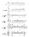
本発明は、図1,2に示す光変調器8に適用される。この光変調器8は、基板11と、基板11上に形成されてなり伝搬する光の位相を変調する導波路12と、この基板11において導波路12を被覆するように積層されるバッファ層14と、変調電界の方向が光の伝搬方向に対して略垂直になるように導波路12の上面に設けられた電極83と、導波路12を介して互いに対向するように設けられた第1の端面84並びに第2の端面85と、第1の端面84と同一の平面を形成するように導波路12の上部に配設される第1の保護材86と、第2の端面85と同一の平面を形成するように導波路12の上部に配設される第2の保護材87と、第1の端面84並びに第1の保護材86の端面86aとの間で形成される平面91上に被着される入射側反射膜93と、第2の端面85並びに第2の保護材87の端面87aとの間で形成される平面92上に被着される出射側反射膜94と、電極83の一端側に配設され周波数fmの変調信号を発振する発振器16と、電極83の他端側に配設される終端抵抗18とを備えている。 The present invention is applied to the
基板11は、例えば引き上げ法により育成された3〜4インチ径のLiNbO3やGaAs等の大型結晶をウェハ状に切り出したものである。この切り出した基板11上には、機械研磨や化学研磨等の処理を施す。The
導波路12は、入射側反射膜93から出射側反射膜94にかけて貫通するように形成され、共振された光を伝搬させるべく形成されている。この導波路12を構成する層の屈折率は、基板11等の他層よりも高く設定されている。導波路12に入射した光は、導波路12の境界面で全反射しながら伝搬する。一般に、この導波路12は、基板11中においてTi原子を拡散させることにより、或いは基板11上へのエピタキシャル成長させることにより作製することができる。 The
なお、この導波路12として、LiNbO3結晶光導波路を適用してもよい。このLiNbO3結晶光導波路は、LiNbO3等からなる基板11表面にTiを拡散させることにより形成することができる。このTiが拡散された領域については他の領域よりも屈折率が高くなるところ、光を閉じ込めることができるため、光を伝搬させることができる導波路12を形成することができる。このような方法に基づいて作製したLiNbO3結晶型の導波路12は、屈折率が電界に比例して変化するポッケルス効果や、屈折率が電界の自乗に比例して変化するカー効果等の電気光学効果を有するため、かかる物理現象を利用して光の変調を行うことができる。Note that a LiNbO3 crystal optical waveguide may be applied as the
バッファ層14は、導波路12における光の伝搬損失を抑えるべくこれを被覆するものである。ちなみに、このバッファ層14の膜厚をあまりに厚くし過ぎると、電界強度が下がり、変調効率が低下するため、光の伝搬損失が大きくならない範囲においてなるべく膜厚を薄く設定するようにしてもよい。 The
電極83は、例えばTiやPt、Au等の金属材料からなり、発振器16から供給された周波数fmの変調信号を導波路12に駆動入力することにより、導波路12内を伝搬する光に位相変調をかける。 The
第1の保護材86並びに第2の保護材87は、それぞれ基板11の材質に対応する部材から構成される。第1の保護材86並びに第2の保護材87は、基板11と同一の材質から構成してもよい。また上記平面91を形成する第1の保護材86の端面86aと第1の端面84とが、互いに同一の結晶方位を有するように加工されていてもよく、同様に上記平面92を形成する第2の保護材87の端面87aと第2の端面85とが、互いに同一の結晶方位を有するように加工されていてもよい。 The first
入射側反射膜93及び出射側反射膜94は、導波路12に入射した光を共振させるために互いに平行となるように設けられたものであり、導波路12を通過する光を往復反射させることにより共振させる共振器5を構成する。 The incident
入射側反射膜93は、図示しない光源から周波数ν1の光が入射される。また、この入射側反射膜93は、出射側反射膜94により反射されて、かつ導波路12を通過した光を反射する。出射側反射膜94は、導波路12を通過した光を反射する。またこの出射側反射膜94は、導波路12を通過した光を一定の割合で外部に出射する。The incident-
なお、これら入射側反射膜93及び/又は出射側反射膜94は、それぞれ平面91,92一面に亘って形成されていてもよいが、導波路12の端部のみを最低限被覆するように形成されていればよい。 The incident-
終端抵抗18は、電極83の終端に取り付けられる抵抗器であり、終端における電気信号の反射を防止することにより、その波形の乱れを防ぐ。 The
図3は、入射側反射膜93が形成される平面91上を図2中A方向から示している。 FIG. 3 shows a
導波路12の光入射端を含む第1の端面84と保護材86の端面86aとにより、同一の平面91が形成されている。この形成される平面91は、傾き0.05°以下である。この傾き0.05°の平面91に対して、1/e2ビーム径10μmの光が傾き0.05°の端面で反射される場合における損失を計算すると、4×10−4であり、入射側反射膜93の反射率と比較して無視できるほど小さい。The
このように第1の端面91並びに第2の端面92を導波路12に対して略垂直に形成させることにより、これに被着される入射側反射膜93並びに出射側反射膜94により光を効率よく共振させることができる。 By forming the
上述の如き構成からなる光変調器8において、入射側反射膜93を介して外部から入射された光は導波路12内を往路方向へ伝搬し出射側反射膜94により反射されるとともに一部外部へ透過する。この出射側反射膜94を反射した光は導波路12内を復路方向へ伝搬して入射側反射膜93により反射される。これが繰り返されることにより、光は導波路12内を共振することになる。 In the
また、光が導波路12内を往復する時間に同期した電気信号を電極83を介して駆動入力とすることにより、光がこの光変調器8内を1回だけ通過する場合と比較して、数十倍以上の深い位相変調をかけることが可能となる。また入射される光の周波数ν1を中心として、数百本ものサイドバンドを広帯域にわたり生成することができる。ちなみに、この生成される各サイドバンドの周波数間隔は、全て入力された電気信号の周波数fmと同等である。このため、光変調器8は、多数のサイドバンドにより構成される光周波数コム発生器としても適用可能となる。Further, by making an electric signal synchronized with the time when the light reciprocates in the
次に、本発明を適用した光変調器8の作製方法につき図4を用いて説明をする。 Next, a manufacturing method of the
先ずステップS11において、LiNbO3結晶からなる基板11の表面にフォトレジストのパターンを作製し、そこにTiを蒸着させる。次にこのフォトレジストを除去することにより、ミクロンサイズの幅で構成されるTiの細線を作製する。First, in step S11, a photoresist pattern is formed on the surface of the
次にステップS12へ移行し、このTiの細線が形成された基板11を加熱することにより、Ti原子を基板11中に熱拡散させて導波路12を形成する。 Next, the process proceeds to step S12, and by heating the
なお、このステップS11、12の導波路12の作製工程においては、Tiを熱拡散させる場合に限定されるものではなく、LiNbO3結晶を安息香酸に浸すことによりLiをH+に置換させるプロトン交換法にこれを代替してもよい。In addition, in the manufacturing process of the
次にステップS13へ移行し、バッファ層14としてのSiO2薄膜を基板11表面に蒸着させる。このステップS13では、SiO2ウェハを基板11表面に貼り付ける方法によりバッファ層14を形成させるようにしてもよい。かかる場合には、後述するステップS14における電極の取り付け領域を考慮して、この蒸着させたバッファ層14を研磨することにより適当な膜圧に制御するようにしてもよい。Next, the process proceeds to step S <b > 13, and a SiO2 thin film as the
次にステップS14へ移行し、バッファ層14上に電極83を形成させる。次にステップS15へ移行し、導波路12の上部において保護材86,87を接着する。この保護材86,87の接着方法については、接着剤で貼り付けるようにしてもよいし、他の手法に基づいて直接的に接合するようにしてもよい。この保護材86,87は、基板11をLiNbO3結晶で構成した場合には、同一材質としてのLiNbO3により構成してもよい。このステップS15においては、貼り付けた保護材86,87につき、それぞれ端面86a,87aが第1の端面84,第2の端面85との間で、それぞれ平面91,92を形成することができるように、切り揃える。Next, the process proceeds to step S <b> 14, and the
最後にステップS16へ移行し、この得られた平面91,92を研磨する。そしてこの研磨された平面91,92上に入射側反射膜93、出射側反射膜94をそれぞれ一面に亘って形成させる。ちなみに、このステップS16においては、平面91,92上に入射側反射膜93、出射側反射膜94を最初に形成させ、次にこれを研磨するようにしてもよい。 Finally, the process proceeds to step S16, and the obtained
このように、本発明を適用した光変調器8では、各端部において保護材86,87を貼り付けて構成するため、従来において、端面最上部の角に位置していた導波路の端面が図3に示すように平面91(92)の略中央部に移動する。その結果、ステップS16における研磨時において平面91(92)の角が欠けた場合においても、導波路12の端面が欠けることがなくなる。即ち、導波路12の端面そのものが欠けにくくなる構成とすることが可能となる。これにより、導波路12の各端面からの光損失を極力抑えることが可能となる。 As described above, in the
また、保護材86,87の材質を基板11の材質に対応する最適な材質で構成することにより、ステップS16における研磨速度を基板11における第1の端面84,第2の端面85から端面86a,87aにかけて均一にすることができる。これにより、導波路12の端面が加工時に丸くなることがなくなり、平坦な研磨面からなる平面91,92を得ることができ、導波路12端面における反射損失を最小限に抑えることが可能となる。また、各平面91,92を構成する端面の結晶方位を同一にすることにより、反射損失を更に抑え込むことも可能となる。 Further, the material of the
さらに、この保護材86,87をあえて設けることにより、ステップS16における研磨の精度が向上し、得られる平面91(92)の導波路12に対する垂直性も向上する。その結果、かかる垂直性の逸脱による光損失も最小限に抑えることが可能となる。 Furthermore, by providing these
また、この保護材86,87を設けることにより、被着すべき入射側反射膜93並びに出射側反射膜94が平面91,92から他の側面に回り込むことによる膜厚の変化を抑えることができる。このため、反射率を確保する上で重要となる導波路12の端面付近の膜厚を最適化することができ、反射率をより向上させることができる。 Further, by providing the
また、入射側反射膜93、出射側反射膜94は、基板11における第1の端面84,第2の端面85から端面86a,87aにかけて広範囲に亘って形成されているため、非常に安定であり、剥がれにくく、さらに製膜の再現性をも向上させることが可能となる。 In addition, the incident-
実際に、保護材86,87を設けたことによる効果を実験的に検証すべく、保護材86,87を貼り付けた後の平面91(92)の研磨を行ったところ、導波路12の端面部分における欠けや曲がりは一切発生せず、入射側反射膜93,出射側反射膜94の被着に適した、平坦な光学研磨が施されていることを確認することができる。 Actually, in order to experimentally verify the effect of providing the
特に第1の保護材86並びに第2の保護材87を、基板11と同一の材質から構成し、また平面91,92を形成する保護材86,87の端面86a,87aと第1の端面84,第2の端面85とが、互いに同一の結晶方位を有するように加工することにより、結晶の硬度が両者間で同一となるため、研磨速度の違いにより平面91,92が傾くこともなくなる。 In particular, the first
このように、本発明を適用した光変調器8では、各端部において保護材86,87を貼り付けることにより、導波路12の端面を平面91(92)の略中央部に移動させることができるため、導波路12の端面の欠けや丸まり、導波路12と平面91,92間の垂直性の確保、平面91,92における研磨精度の向上、入射側反射膜93及び出射側反射膜94の剥がれや回り込みの抑制、入射側反射膜93及び出射側反射膜94における反射率の向上、設計した反射特性の実現、反射膜の性能再現性向上が可能となる。その結果、入射側反射膜93及び出射側反射膜94より構成される共振器5のフィネスを向上させることができ、性能のよい光変調器、光周波数コム発生器を再現性よく作製することが可能となり、歩留まりを向上させることも可能となる。 As described above, in the
実際に上述の構成からなる光変調器8を、研磨された平面91,92上において、反射率97%からなる反射膜93,94を被着させることにより作製した結果、導波路12の結晶長を27.4mmとした場合(以下、短共振器という。)において、最高61ものフィネスを得ることができ、また、導波路12の結晶長を54.7mmとした場合(以下、長共振器という。)において、最高38ものフィネスを得ることができた。従来の導波路型の光共振器(IEEE Photonics Technology Letters,Vol.8, No. 10,1996)のフィネスは、30が最高であったことから、この端面研磨、コーティングの精度を向上させた光変調器8は、フィネスを大幅に向上させることができることが分かる。特に、作製した光変調器8のサンプル6個全てにつき、30以上のフィネスを得ることができ、作製プロセスの再現性が高いことも示されている。 As a result of actually manufacturing the
図5は、導波路12における往路方向又は復路方向のうち何れか一の伝搬方向あたりの共振器5の内部損失を示している。この図5では、上述した長共振器で構成される光変調器8につきの伝搬方向あたりの損失を3個のサンプルに亘り測定してプロットし(図中丸印で示す)、また短共振器で構成される光変調器8につきの伝搬方向あたりの損失を3個のサンプルに亘り測定してプロットし(図中四角で示す)、得られた各プロットを直線で近似している。 FIG. 5 shows the internal loss of the
この得られた直線より、長さlの共振器5の導波路12における伝搬方向あたりの内部損失Lsは、反射膜93,94における反射率をR、導波路12における単位長さあたりの損失をαとするとき、損失そのものが小さい場合においてLs=αl−lnRで表される。測定されたフィネスをFとしたとき、一伝搬方向あたりの損失Lsは、Ls=π/Fと求められる。測定したフィネスFから内部損失Lsを求め、これをグラフ化すると、図5に示すように導波路12の結晶長が長くなるにつれ、導波路12による内部損失が増加することが分かる。 From the obtained straight line, the internal loss Ls per propagation direction in the
ちなみに、この図5において共振器5の長さが0である場合における内部損失は、結晶端面において生じた損失に基づくものである。即ち、反射率97%(透過率3%)の反射膜93,94がコーティングされているため、最低3%の損失が生じることになる。しかしこの図5より、平面91,92における反射膜93,94への透過以外に目立った損失がないことが分かる。 Incidentally, the internal loss when the length of the
同様に、この光変調器8を光周波数コム発生器に応用した場合には、保護材86,87を貼り付けた状態で平面91,92の研磨と入射側反射膜93及び出射側反射膜94の被着を行うため、これら反射膜93,94の反射率を向上させることが可能となる。その結果、光共振器5のフィネスを向上させることができ、サイドバンドの発生周波数帯域を拡大させることもできる。 Similarly, when this
ちなみに、この光変調器8を光周波数コム発生器に応用する場合には、入射側反射膜93を、導波路12内へ入射させる光のみ透過させ、導波路12内において発生させたサイドバンドを反射する狭帯域フィルタに置換してもよい。このような狭帯域フィルタに置換することにより、入射させる光からサイドバンドへの変換効率を向上させることができる。 Incidentally, when this
同様に、出射側反射膜94は、出力スペクトルフラット化のためのフィルタに置換してもよい。通常の光周波数コム発生器において、得られるサイドバンドの光強度は、その次数の増加とともに指数関数的に減少する。そこで出射側反射膜94を、次数に応じた光強度の減少を相殺するような特性を持つフィルタに代替させることにより、得られる各サイドバンドの光強度を平坦化させることが可能となる。 Similarly, the output
なお、入射側反射膜93及び出射側反射膜94それぞれにつき、上述した各フィルタに置換してもよいし、何れか一方の反射膜93,94につき上述した各フィルタに置換してもよい。 Note that each of the incident-
なお、本発明を適用した光変調器8並びにこれを応用した光周波数コム発生器は、平面91,92に対して直接的に入射側反射膜93並びに出射側反射膜94を形成させるモノリシック型で構成されている。換言すれば、この光変調器8は、平面91,92と空間的に離間した位置に各反射膜93,94を設ける構成ではないため、共振器5のFSR(Free Spectral Range)は、ステップS16における研磨後の導波路12を構成する結晶の平面91から平面92に至るまでの結晶長さに支配される。このため、光変調器8は、光共振器5のFSRの整数倍が所望の変調周波数となるようにきわめて精密な結晶長さの制御が要求される。 The
例えば、共振器5のFSRを周波数fFSRに一致させる場合、導波路12の群屈折率ngと、入射側反射膜93及び出射側反射膜94の群遅延時間の平均値τgを考慮して、導波路12の結晶長さ(基板11における第1の端面84から第2の端面85に至るまでの間隔)Lを以下の式(1)
L=c/2ngfFSR−cτg/ng・・・・・・・・・・・(1)
(cは真空中の光速度)
に合わせることにより、共振器5のFSRをfFSRに一致させることができ、変調効率を大幅に向上させることが可能となる。For example, when making the FSR of the
L = c / 2n g f FSR -cτ g / n g ··········· (1)
(C is the speed of light in vacuum)
Therefore, the FSR of the
なお本発明は、上述した実施の形態に限定されるものではない。例えば図6に示すような光変調器9にも適用することができる。この光変調器9において上述した光変調器8と同一の構成、要素については、図1,2における説明を引用し、ここでの説明を省略する。 The present invention is not limited to the above-described embodiment. For example, the present invention can be applied to an optical modulator 9 as shown in FIG. In this optical modulator 9, the same configurations and elements as those of the
光変調器9は、基板11と、基板11上に形成されてなり伝搬する光の位相を変調する導波路12と、導波路12の上面に設けられたウェハ95と、変調電界の方向が光の伝搬方向に対して略垂直になるようにウェハ95の上面に設けられた電極83と、導波路12を介して互いに対向するように設けられた第1の端面84並びに第2の端面85と、第1の端面84並びにウェハ95の端面96aとの間で形成される平面101上に被着される入射側反射膜93と、第2の端面85並びにウェハ95の端面97aとの間で形成される平面102上に被着される出射側反射膜94とを備えている。 The optical modulator 9 includes a
この光変調器9においても、上述した光変調器8と同様に、周波数fmの変調信号を発振する図示しない発振器と、図示しない終端抵抗が接続される。 Also in this optical modulator 9, similarly to the
ウェハ95は、SiO2等からなり、導波路12と略同一の長さでコ字状となるように構成される。このウェハ95は端部のみ厚く構成され、電極83が配設される中央部分のみ薄く構成する。これにより導波路12内を伝搬する光につき電極83から変調電界を効率よく印加することができる。The
このウェハ95は、上述したバッファ層14としての役割を担い、基板11の表面直下に形成されてなる導波路12を被覆することにより光損失を抑える。またこのウェハ95は、上述した光変調器8における第1の保護材86並びに第2の保護材87としての役割も担い、それぞれ端面96a,97aが第1の端面84,第2の端面85との間で、それぞれ平面101,102を形成することができるように切り揃えられている。 The
このウェハ95を配設する場合には、端部の厚みに合わせたSiO2のウェハを基板11上に貼り付け、次に電極83を設ける部分につき切削していくことで、図6に示すようなコ字状に仕上げることが可能となる。When this
即ち、この光変調器9は、光変調器8と同等の効果が得られるとともに、保護材を取り付ける手間を省くことができるという利点がある。 That is, the optical modulator 9 has the advantage that the same effect as the
なお本発明は、上述した実施の形態に限定されるものではない。例えば図7に示すような往復変調型の光変調器51にも適用することができる。この光変調器51において上述した光変調器8と同一の構成、要素については、図1,2における説明を引用し、ここでの説明を省略する。 The present invention is not limited to the above-described embodiment. For example, the present invention can also be applied to a reciprocating modulation type
光変調器51は、図7(a)に示すように、基板11と、基板11上に形成されてなり伝搬する光の位相を変調する導波路12と、この基板11において導波路12を被覆するように積層されるバッファ層14と、変調電界の方向が光の伝搬方向に対して略垂直になるように導波路12の上面に設けられた電極83と、導波路12の上部に配設される第1の保護材86並びに第2の保護材87と、平面91上に被着される反射防止膜63と、平面92上に被着される出射側反射膜94とを備えている。 As shown in FIG. 7A, the
また、この光変調器51を実際に使用する場合には、更に図7(b)に示すように、図示しない光源からの入力光を伝送し或いは光変調器51から出力される出力光を外部へ伝送するための光ファイバ等で構成される光伝送路23と、上記入力光並びに出力光を分離するための光サーキュレータ21と、この光サーキュレータ21に光接続されるフォーカサー22からなる光学系が実装され、電極83の一端側に配設され周波数fmの変調信号を発振する発振器16と、電極83の他端側に配設される終端抵抗18とがさらに配設される。 Further, when the
反射防止膜63は、第1の端面84並びに第1の保護材86の端面86aとの間で形成される平面91上に被着される。この反射防止膜63は、低反射膜により構成されていてもよいし、無コートで構成することにより、低反射膜を被着したのと同等の効果が得られるようにしてもよい。 The
フォーカサー22は、光サーキュレータ21を通過した入力光を導波路12の端部へ集束させるとともに、導波路12の端部から反射防止膜63を透過した出力光を集光してこれを光サーキュレータ21へ送る。このフォーカサー22は、導波路12の径に応じたスポット径となるように入力光を光結合させるためのレンズ等で構成してもよい。 The
このような構成からなる光変調器51は、導波路12の一の端部につき高反射膜としての出射側反射膜94を設け、他の端部につき反射防止膜63を設けることにより、いわゆる往復変調型の光変調器として動作する。導波路12に入射された入力光は、導波路12を伝搬しながら変調され、端面の出射側反射膜94により反射された後、再び導波路12を伝搬して反射防止膜63を透過してフォーカサー22側に出射され出力光となる。同時に、発振器16から供給される周波数fmの電気信号は、入力光を変調しつつ電極83上を伝搬した後、終端抵抗18により吸収されることになる。 The
また、この光変調器51は、図7(c)に示すように、発振器25並びに終端抵抗27を電極83の一端側に設け、発振器25から供給される電気信号を電極83上において伝搬させた上で、これを電極83の他端側で反射させるようにしてもよい。このとき、発振器25から供給される電気信号と、電極83の他端側で反射された電気信号を分けるためのアイソレータ26を設けるようにしてもよい。また、この光変調器51では、反射率の高い入射側反射膜93を被着させる。これにより導波路12内部において光を共振させることができる。また、この入射側反射膜93の代替として、上述した低反射率の反射防止膜63を被着させるようにしてもよい。これにより、光を導波路12内において一度だけ往復させつつ、位相変調を施すことも可能となる。 Further, as shown in FIG. 7C, the
この光変調器51では、出射側反射膜94により反射される光の位相に合わせて電気信号の反射位相を調整することにより、電極83を往復する電気信号それぞれにより光の位相を変調させることができるため、変調効率を増大させることができる。特に、保護材86,87を貼り付けることにより、上述の如く膜63,94の剥がれや欠け等を抑え、フィネスをより向上させた光変調器51では、光変調効率をさらに増大させることが可能となる。 In this
また、これら光変調器51を光周波数コム発生器に適用した場合において、電極を往復する電気信号により、導波路12内で共振する光につき往復変調を施すことが可能となる。かかる場合において、発生させたサイドバンドの各周波数(波長)における強度分布は、図8に示すように、電極83へ印加する電気信号の変調周波数を25GHzとし、そのパワーを0.5Wとした場合において、導波路12内に加わる変調の大きさとして表される変調指数は、伝搬方向あたりπラジアンである。この結果より、位相を半波長動かすために必要な電圧として定義される半波長電圧Vπは、7.1Vであることが分かる。 Further, when these
短共振器で構成される光変調器8は、長共振器で構成される光変調器8と比較して、上述の如くフィネスが高い分、サイドバンドの発生の効率は高く、またサイドバンドの発生周波数帯域幅Δfは11THzに達する。また、短共振器で構成される光変調器8の電極83の長さは、僅か20mmであるが、長共振器で構成される光変調器8と比較して遜色のない変調効率が得られる。即ち、往復変調が有効に作用していることが分かる。 The
なお、この光変調器51は、電気信号を反射させる代わりに、信号源としての発振器16の出力を分割することにより、電極83の両端から電気信号を別々に駆動入力するようにしてもよいし、電極83の両端にそれぞれ別の発振器16を接続することにより、これを実行するようにしてもよい。 The
なお本発明は、例えば図9に示すような光導波路型のレーザ発振器52にも適用することができる。このレーザ発振器52において、上述した光変調器8と同一の構成、要素については、図1,2における説明を引用し、ここでの説明を省略する。 The present invention can also be applied to, for example, an optical waveguide
レーザ発振器52は、図9に示すように、基板11と、基板11上に形成されてなる導波路12と、この基板11において導波路12を被覆するように積層されるバッファ層14と、導波路12の上部に配設される第1の保護材86並びに第2の保護材87と、平面91上に被着される入射側反射膜93と、平面92上に被着される出射側反射膜94とを備え、入射側反射膜93と出射側反射膜94との間で共振器5を構成する。また、このレーザ発振器52を実際に使用する場合には、波長λ0の光を出射する励起光源28が実装される。As shown in FIG. 9, the
このレーザ発振器52における導波路12中には、例えばエルビウムイオンのような、入射側反射膜93を介して入射された光を吸収して媒質固有の光の波長に対して増幅特性を有する増幅媒質を拡散させる。これにより、導波路12を光の増幅媒質として働かせることが可能となる。またこのような増幅媒質としての導波路12に対して、適当な波長の光を入射させると、エネルギー準位で決まる固有の波長に対する光の増幅器として作用することになる。また、自然放出遷移により発生した光を増幅して発振する発振器としても作用することになる。レーザ発振するのは、共振器5内における増幅率が損失率を上回った場合であるから、保護材86,87を貼り付けて反射膜93,94の剥がれや欠け等を防止しつつ導波路12の端面における反射特性を高めることにより、共振器5内の損失率も低くなることから、レーザ発振の閾値を低下させることができる。 In the
ちなみに、このレーザ発振器52を光パラメトリック発振器として適用してもよい。かかる場合には、発振が起こるのは共振器5内の増幅率が損失率を上回った場合であるから、保護材86,87を貼り付けた反射膜93,94の剥がれや欠けのない高フィネスの共振器5を構成することにより、発振の閾値を低下させることができる。 Incidentally, this
導波路12内に特別な増幅媒質を導入しなくても、この導波路12としてLiNbO3結晶のような非線形光学結晶で構成することにより、導波路12内に入射される光によって誘起される非線形分極により、当該入射される光とは異なる波長に増幅利得を持たせることが可能となる。例えば、周期分極反転構造を持つ非線形光学結晶を用いても導波路12を構成して良い。Even if a special amplifying medium is not introduced into the
このレーザ発振器52における共振器5を構成する入射側反射膜93は、励起光源28からの光に対して低反射率であり、かつ導波路12により発振される光の波長に対して高反射率の膜を使用してもよい。また、この共振器5を構成する出射側反射膜94は、導波路12により発振される光の波長に対して最適な出力カップリングが可能な反射率を有する膜を使用してもよい。 The incident-
上述の如くレーザ発振器52やこれを適用する光パラメトリック発振器において導波路12を用いる利点は、光を狭い領域に閉じ込めることができることと、電界強度が高めることができることによる増幅率の向上である。特にこのレーザ発振器52等では、従来の発振器と比較して高いフィネスを得ることができるため、導波路12を用いることの利点がさらに助長されることになる。 As described above, the advantage of using the
なお本発明は、例えば図10に示すようなモードが同期された光を発振するレーザ発振器53にも適用することができる。このモードが同期された光とは、等しい周波数間隔で発振している多数のモードの位相を揃えたものである。このレーザ発振器53において、上述した光変調器8並びにレーザ発振器52と同一の構成、要素については、図1,2,9における説明を引用し、ここでの説明を省略する。 The present invention can also be applied to, for example, a
レーザ発振器53は、図10(a),(b)に示すように、基板11と、基板11上に形成されてなり伝搬する光の位相を変調する導波路12と、この基板11において導波路12を被覆するように積層されるバッファ層14と、変調電界の方向が光の伝搬方向に対して略垂直になるように導波路12の上面に設けられた電極83と、導波路12の上部に配設される第1の保護材86並びに第2の保護材87と、平面91上に被着される入射側反射膜93と、平面92上に被着される出射側反射膜94とを備え、入射側反射膜93と出射側反射膜94との間で共振器5を構成する。また、このレーザ発振器53を実際に使用する場合には、波長λ0の光を出射する励起光源28が実装され、更に電極83の一端側に配設され周波数fmの変調信号を発振する発振器16と、電極83の他端側に配設される終端抵抗18とが配設される。この入射側反射膜93と出射側反射膜94とは、それぞれレーザ発振する多モード間の位相同期をとる機能を有する。As shown in FIGS. 10A and 10B, the
このような構成からなるレーザ発振器53では、上述したレーザ発振器52において導波路12の上部に電極83を配設することにより、各モードにつき同期がとられたモード同期レーザの発振が可能となる。ここで、共振器5のFSRの整数倍に一致する周波数の変調信号を発振器16から駆動入力することにより、多モードの光を発振する導波路12の電気光学効果に基づき、各モードの位相同期が施される結果、モード同期レーザを発振するレーザ発振器として動作することになる。 In the
このモード同期が施されると、レーザ発振器53より発振される光の時間波形は、増幅周波数帯域幅の逆数程度の時間幅を持つ短パルスとなる。また、周波数軸の波形は、一定の周波数間隔でサイドバンドが配列する光周波数コムとなる。このため、レーザ発振器53に対する制御を最適化させることにより、光の周波数測定への応用や多波長光源への応用も可能となる。またこのレーザ発振器53を、上述したレーザ発振器52と同様に光パラメトリック発振器として適用してもよいことは勿論である。特にこのレーザ発振器53は、保護材86,87が貼り付けられているため反射膜93,94の剥がれや欠けがなく、共振器5全体のフィネスを向上させることができ、モード同期レーザを効率よく発振させることが可能となる。 When this mode synchronization is performed, the time waveform of the light oscillated from the
ちなみに、レーザ発振器53におけるモード同期は、上述した電気光学効果を利用するものに限定されるものではなく、共振器5内における光学素子の非線形効果を利用するものであればいかなる現象に基づくものであってもよい。例えば、LiNbO3結晶を導波路12に用いることにより、その効果をより際立たせることも可能となる。Incidentally, the mode synchronization in the
なお本発明は、例えば図11に示すような変形ファブリペロー(FP)電気光学変調器54にも適用することができる。この変形FP電気光学変調器54において、上述した光変調器8並びにレーザ発振器52と同一の構成、要素については、図1,2,9における説明を引用し、ここでの説明を省略する。 The present invention can also be applied to a modified Fabry-Perot (FP) electro-
変形FP電気光学変調器54は、図11に示すように、基板11と、基板11上に形成されてなり伝搬する光の位相を変調する導波路12と、この基板11において導波路12を被覆するように積層されるバッファ層14と、変調電界の方向が光の伝搬方向に対して略垂直になるように導波路12の上面に設けられた電極83と、導波路12の上部に配設される第1の保護材86並びに第2の保護材87と、平面91上に被着される入射側反射膜93と、平面92上に被着される出射側反射膜94とを備え、入射側反射膜93と出射側反射膜94との間で共振器5を構成する。また、このレーザ発振器53を実際に使用する場合には、反射鏡31が実装され、必要な場合には、更に電極の一端側に配設され周波数fmの変調信号を発振する図示しない発振器と、電極の他端側に配設される図示しない終端抵抗とが配設される。 As shown in FIG. 11, the modified FP electro-
反射鏡31は、外部から供給される光を透過させ変形FP電気光学変調器54側の導波路12の端部へ導くとともに、当該導波路12の端部から出射された光を反射する。即ち、この反射鏡31を設けることにより、導波路12内へ入射させる光のみ透過させ、導波路12内で発生させたサイドバンドを反射することができるため、入射させる光からサイドバンドへの変換効率を向上させることができる。即ち、このような構成からなる変形FP電気光学変調器54では、入射側反射膜93を、導波路12内へ入射させる光のみ透過させ発生させたサイドバンドを反射する狭帯域フィルタに置換した場合と同様の効果を得ることができる。特にこの変形FP電気光学変調器54では、保護材86,87が貼り付けられているため反射膜93,94の剥がれや欠けがなく、共振器5全体のフィネスを向上させることができるため、サイドバンドへの変換効率をより高めることが可能となる。 The reflecting
なお、本発明を適用した光変調器8は更に以下に説明する通信システム55に適用することもできる。 The
通信システム55は、例えば、WDM通信方式に基づいて符号分割多重接続を行うシステムが適用され、図12(a)に示すように、歩行者が携帯可能な移動体端末としての携帯通信機器57と、携帯通信機器57との間で無線信号を送受信を行うことにより通信を中継するための複数の基地局58と、接続された光ファイバ通信網35,38を介して基地局58を含めたネットワーク全体における通信を制御するホスト制御装置59とを備えている。 As the
携帯通信機器57は、各地区に設けられた基地局58との間で無線信号を送受信すべく、車載或いは携帯できるように構成されている。即ち、この携帯通信機器57は、例えばファクシミリ通信やパーソナルコンピュータ等に搭載されてデータ通信を行うための装置を含むものであるが、一般には音声による通話を行うための携帯電話やPHS(パーソナルハンディホンシステム)等であり、特に小型軽量で携帯性に特化した機器として構成されている。 The
各基地局58には、図12(a)に示すように光変調器8が搭載される。光変調器8における電極83には、携帯通信機器57との間でマイクロ波を送受信するためのアンテナ33が接続されている。また、この光変調器8は、ホスト制御装置59から光ファイバ通信網35を介して伝送された光の一部が入射側反射膜93を介して導波路12内へ入射される。この導波路12内へ入射された光は、略平行に配設された入射側反射膜93並びに出射側反射膜94により共振されることになる。またこの光変調器8では、携帯通信機器57から供給されるマイクロ波をアンテナ33を介して受信し、かかるマイクロ波に応じた変調信号を電極83を介して導波路12内を伝搬する光に印加することができるため、携帯通信機器57からの送信情報に応じた位相変調をこれに施すことが可能となる。なお、光変調器8は、位相変調した光を出射側反射膜94を介して出射させる。出射された光は光ファイバ通信網38を介してホスト制御装置59へ伝送されることになる。 Each
ホスト制御装置59は、基地局58へ伝送するための光を発生させ、また基地局58において変調された光を光電変換して検波出力を得る。即ち、このホスト制御装置59は、様々な基地局からの検波出力を一括管理することができる。 The
このような通信システム55では、ホスト制御装置59から出力された光を光ファイバ通信網35を介して基地局58へ伝送する。基地局58は、この伝送された光を光変調器8における導波路12内を伝搬させるとともに、更にマイクロ波に応じた位相変調を施した上で、光ファイバ通信網38を介してこれをホスト制御装置59へ伝送する。 In such a
即ち、基地局58へ伝送される光は、当該基地局58周辺にある携帯通信機器57から発呼された場合に、上述したマイクロ波に含まれる通話内容に応じた位相変調が施されることになる。一方、この基地局58へ伝送される光は、当該基地局58周辺にある携帯通信機器57から発呼されなかった場合に、上述した位相変調が施されることはなくなる。ホスト制御装置59では、基地局58から光ファイバ通信網38を介して伝送される光につき位相変調が施されていた場合には、これを光電変換することにより、通話内容に応じた検波出力を取得することが可能となる。 That is, the light transmitted to the
この通信システム55では、保護材86,87を貼り付けた高フィネスの共振器を有する光変調器8を基地局58へ搭載するため、導波路12内を伝搬する光の往復回数を増やすことができ、光変調器8自体の感度を向上させることが可能となる。 In this
なお、この通信システム55では、図12(b)に示すように、一芯双方向で光伝送するようにしてもよいことは勿論である。 In this
さらに、本発明を適用した光変調器8では、図1に示すように導波路12の往路方向(復路方向)の結晶長LC1を27mm(又は54mm)程度になるように調整されていてもよい。かかる結晶長にすることにより奏する効果につき、以下において説明する。 Further, in the
導波路12における往路方向(復路方向)へ伝播する光の損失率をLo1としたとき、かかる損失率Lo1と導波路12の結晶長LC1との関係を図13(a)に示す。結晶長LC1が増加していくにつれて、伝播する光の損失は徐々に大きくなることが示されている。また図13(b)は、かかる結晶長LC1に対するフィネスの関係を示している。この図13(b)に示すようにフィネスは、一般にπ/Lo1で表されるが、結晶長LC1が小さいほど高くなることがわかる。 FIG. 13A shows the relationship between the loss rate Lo1 and the crystal length LC1 of the
光変調器8の性能指数は、Vπ/(フィネス)で表すことができる(Vπは光位相をπラジアン変調するために要する電圧)。この性能指数が小さいほど光変調器8として、また当該光変調器8を用いた光周波数コム発生器として、性能がより優れていることになる。 The figure of merit of the
図14は、これらフィネスや損失率Lo1に基づいて計算した性能指数を結晶長LC1との関係において示している。この図14において、lmは、結晶長LC1に対する電極83の長さの差分を表している。一般に導波路12の両端から数mmは電極を設けることができないため、このlmを6mmとした場合と、lmを1mmとした場合を例に挙げて計算をしている。 FIG. 14 shows the figure of merit calculated based on these finesse and loss rate Lo1 in relation to the crystal length LC1. In FIG. 14, lm represents the difference in the length of the
この図14に示すようにlm=6mmである場合において、結晶長LC1が15〜30mmのときに性能指数が小さくなることが分かる。またかかる性能指数の結晶長LC1に対応するFSRをプロットすると、2.5GHz付近において最も優れた性能となることが分かる。ちなみに、この図14における傾向をシミュレーションする上において、変調周波数を25GHzとし、電極83によるマイクロ波の伝送損失を−10dB/50mm@25GHzと仮定し、さらに変調効率は、往復変調時においてPin=0.43W、結晶長LC1=27mm(電極83の長さが21mmのとき)である場合に変調指数がπラジアンであることを考慮し、さらに光の伝送損失αが−0.0106/cmである場合を仮定している。また、ミラーの反射率は、結晶長に応じた損失率に対して最適化されている。 As shown in FIG. 14, in the case where lm = 6 mm, the figure of merit becomes small when the crystal length LC1 is 15 to 30 mm. Further, when the FSR corresponding to the crystal length LC1 of such a figure of merit is plotted, it can be seen that the best performance is obtained in the vicinity of 2.5 GHz. Incidentally, in simulating the tendency in FIG. 14, it is assumed that the modulation frequency is 25 GHz, the microwave transmission loss by the
このため、lm=6mmである場合において、導波路12の結晶長LC1を27mm程度とすることにより、光変調器8としての性能をより向上させることが可能となる。ちなみに、この結晶長LC1は27mmにある場合に限定されるものではなく、24±6mmの範囲であればいかなる長さで構成されていてもよい。なお、実用上の結晶長LC1は、光通信分野における時分割多重化(TDM:Time Division Multiplex)光通信における10GHzや波長割多重化(WDM:Wavelenth Division Multiplex)光通信における25GHzの最大公約数である5GHzの整数分の1とするのが好適であり、27mmは2.5GHzに相当している。 For this reason, when lm = 6 mm, the performance as the
また、結晶長LC1に対応するFSRのプロットが1.25GHzである場合においても、同様に優れた性能が示されることから、これに対応する結晶長LC1を54mm程度で構成してもよい。 Further, even when the FSR plot corresponding to the crystal length LC1 is 1.25 GHz, excellent performance is similarly shown. Therefore, the corresponding crystal length LC1 may be configured to be about 54 mm.
またlm=1mmである場合においても、同様にシミュレーションすると、10GHz程度で優れた性能が示されることから、結晶長LC1をこれに対応させることで、光変調器8としての性能をより高めることが可能となる。 Further, even in the case of lm = 1 mm, if the same simulation is performed, an excellent performance is shown at about 10 GHz. Therefore, the performance as the
8 光変調器、11 基板、12 導波路、14 バッファ層、16 発振器、18 終端抵抗、83 電極、84 第1の端面、85 第2の端面、86 第1の保護材、87 第2の保護材、91,92 平面、93 入射側反射膜、94 出射側反射膜 8 optical modulator, 11 substrate, 12 waveguide, 14 buffer layer, 16 oscillator, 18 termination resistor, 83 electrode, 84 first end face, 85 second end face, 86 first protective material, 87 second protection Material, 91,92 plane, 93 incident side reflection film, 94 emission side reflection film
Claims (19)
Translated fromJapanese上記入射側反射膜から上記出射側反射膜にかけて貫通するように形成され、上記共振手段により共振された光を伝搬させる光導波路と、
上記光導波路を上面から形成させるための基板と、
上記基板と同じ硬さを持つ部材から構成され、上記部材における少なくとも一の端面が上記光導波路における光入射端又は光出射端を含む上記基板の端面と同一の平面を形成するように上記光導波路の上部に配設される端面保護手段とを備え、
上記入射側反射膜並びに上記出射側反射膜は、上記部材の端面と上記基板の端面を研磨することにより形成される平面にそれぞれ被着されてなること
を特徴とする光共振器。A resonance means configured to resonate light incident through the incident-side reflection film, the incident-side reflection film and the emission-side reflection film being parallel to each other;
An optical waveguide that is formed so as to penetrate from the incident-side reflection film to the emission-side reflection film, and that propagates the light resonated by the resonance means;
A substrate for forming the optical waveguide from above;
The optical waveguide is composed of a member having thesame hardness as the substrate,and at least one end surface of the member forms the same plane as the end surface of the substrate including a light incident end or a light emitting end of the optical waveguide. An end face protection means disposed on the upper part of
The optical resonator according to claim 1, wherein the incident-side reflection film and the emission-side reflection film are respectively attached to a plane formed by polishing an end face of the member and an end face of the substrate.
を特徴とする請求項1記載の光共振器。2. The member constituting the end face protection means is made of the same material as the substrate, and the end face of the member forming the plane and the end face of the substrate have the same crystal orientation. The optical resonator as described.
互いに平行な入射側反射膜及び出射側反射膜より構成され、入射側反射膜を介して入射された光を共振させる共振手段と、
上記入射側反射膜から上記出射側反射膜にかけて貫通するように形成され、上記発振手段から供給された上記変調信号に応じて上記共振手段により共振された光の位相を変調する光導波路と、
上記光導波路を上面から形成させるための基板と、
上記基板と同じ硬さを持つ部材から構成され、上記部材における少なくとも一の端面が上記光導波路における光入射端又は光出射端を含む上記基板の端面と同一の平面を形成するように上記光導波路の上部に配設される端面保護手段とを備え、
上記入射側反射膜並びに上記出射側反射膜は、上記部材の端面と上記基板の端面を研磨することにより形成される平面にそれぞれ被着されてなること
を特徴とする光共振器。Oscillating means for oscillating a modulation signal of a predetermined frequency;
A resonance means configured to resonate light incident through the incident-side reflection film, the incident-side reflection film and the emission-side reflection film being parallel to each other;
An optical waveguide that is formed so as to penetrate from the incident-side reflection film to the emission-side reflection film, and modulates the phase of the light resonated by the resonance means according to the modulation signal supplied from the oscillation means;
A substrate for forming the optical waveguide from above;
The optical waveguide is composed of a member having thesame hardness as the substrate,and at least one end surface of the member forms the same plane as the end surface of the substrate including a light incident end or a light emitting end of the optical waveguide. An end face protection means disposed on the upper part of
The optical resonator according to claim 1, wherein the incident-side reflection film and the emission-side reflection film are respectively attached to a plane formed by polishing an end face of the member and an end face of the substrate.
L=c/2ngfFSR−cτg/ng
(cは真空中の光速度、ngは上記光導波路の群屈折率、fFSR は上記変調手段のFSR(Free Spectral Range)、τgは入射側反射膜及び出射側反射膜の群遅延時間の平均値) であることを特徴とする請求項9記載の光変調器。The interval L between the end faces of the substrate is
L = c / 2n g f FSR -cτ g / n g
(C is the velocity of light in vacuum,ng is the group refractive index of the optical waveguide, fFSR is the FSR (Free Spectral Range) of the modulation means, and τg is the group delay time of the incident side reflection film and the emission side reflection film. The optical modulator according to claim 9, wherein
互いに平行な入射側反射膜及び出射側反射膜より構成され、入射側反射膜を介して入射された光を共振させる共振手段と、
上記入射側反射膜から上記出射側反射膜にかけて貫通するように形成され、上記検出手段により検出された電気信号の波長に応じて上記共振手段により共振された光の位相を変調する光導波路と、
上記光導波路を上面から形成させるための基板と、
上記基板と同じ硬さを持つ部材から構成され、上記部材における少なくとも一の端面が上記光導波路における光入射端又は光出射端を含む上記基板の端面と同一の平面を形成するように上記光導波路の上部に配設される端面保護手段とを備え、
上記入射側反射膜並びに上記出射側反射膜は、上記部材の端面と上記基板の端面を研磨することにより形成される平面にそれぞれ被着されてなること
を特徴とする光変調器。Detection means for detecting an electrical signal;
A resonance means configured to resonate light incident through the incident-side reflection film, the incident-side reflection film and the emission-side reflection film being parallel to each other;
An optical waveguide that is formed so as to penetrate from the incident-side reflection film to the emission-side reflection film, and modulates the phase of the light resonated by the resonance means according to the wavelength of the electrical signal detected by the detection means;
A substrate for forming the optical waveguide from above;
The optical waveguide is composed of a member having thesame hardness as the substrate,and at least one end surface of the member forms the same plane as the end surface of the substrate including a light incident end or a light emitting end of the optical waveguide. An end face protection means disposed on the upper part of
The light modulator according to claim 1, wherein the incident-side reflection film and the emission-side reflection film are respectively attached to a plane formed by polishing an end face of the member and an end face of the substrate.
互いに平行な入射側反射膜及び出射側反射膜より構成され、入射側反射膜を介して入射された光を共振させる共振手段と、
上記入射側反射膜から上記出射側反射膜にかけて貫通するように形成され、上記発振手段から供給された上記変調信号に応じて上記共振手段により共振された光の位相を変調し、上記入射された光の周波数を中心としたサイドバンドを上記変調信号の周波数の間隔で生成する光導波路と、
上記光導波路を上面から形成させるための基板と、
上記基板と同じ硬さを持つ部材から構成され、上記部材における少なくとも一の端面が上記光導波路における光入射端又は光出射端を含む上記基板の端面と同一の平面を形成するように上記光導波路の上部に配設される端面保護手段とを備え、
上記入射側反射膜並びに上記出射側反射膜は、上記部材の端面と上記基板の端面を研磨することにより形成される平面にそれぞれ被着されてなること
を特徴とする光周波数コム発生器。Oscillating means for oscillating a modulation signal of a predetermined frequency;
A resonance means configured to resonate light incident through the incident-side reflection film, the incident-side reflection film and the emission-side reflection film being parallel to each other;
It is formed so as to penetrate from the incident side reflection film to the emission side reflection film, and modulates the phase of the light resonated by the resonance means in accordance with the modulation signal supplied from the oscillation means, and is incident An optical waveguide that generates sidebands centered on the frequency of light at intervals of the frequency of the modulation signal;
A substrate for forming the optical waveguide from above;
The optical waveguide is composed of a member having thesame hardness as the substrate,and at least one end surface of the member forms the same plane as the end surface of the substrate including a light incident end or a light emitting end of the optical waveguide. An end face protection means disposed on the upper part of
The optical frequency comb generator, wherein the incident-side reflection film and the emission-side reflection film are respectively attached to a plane formed by polishing an end face of the member and an end face of the substrate.
上記入射側反射膜から上記出射側反射膜にかけて貫通するように形成され、上記共振手段により共振された光を増幅させるとともに、これを出射側反射膜を介して外部へ出射させる光導波路と、
上記光導波路を上面から形成させるための基板と、
上記基板と同じ硬さを持つ部材から構成され、上記部材における少なくとも一の端面が上記光導波路における光入射端又は光出射端を含む上記基板の端面と同一の平面を形成するように上記光導波路の上部に配設される端面保護手段とを備え、
上記入射側反射膜並びに上記出射側反射膜は、上記部材の端面と上記基板の端面を研磨することにより形成される平面にそれぞれ被着されてなること
を特徴とする光発振器。Resonating means that is composed of an incident side reflection film and an emission side reflection film that are parallel to each other, and resonates light incident through the incident side reflection film or light generated by laser amplification;
An optical waveguide that is formed so as to penetrate from the incident-side reflection film to the emission-side reflection film, amplifies the light resonated by the resonance means, and emits the light to the outside through the emission-side reflection film;
A substrate for forming the optical waveguide from above;
The optical waveguide is composed of a member having thesame hardness as the substrate,and at least one end surface of the member forms the same plane as the end surface of the substrate including a light incident end or a light emitting end of the optical waveguide. An end face protection means disposed on the upper part of
The optical oscillator, wherein the incident-side reflection film and the emission-side reflection film are respectively attached to a plane formed by polishing an end face of the member and an end face of the substrate.
互いに平行な入射側反射膜及び出射側反射膜より構成され、入射側反射膜を介して入射された光、又はレーザ増幅により発生された光を共振させる共振手段と、
上記入射側反射膜から上記出射側反射膜にかけて貫通するように形成され、上記発振手段から供給された上記変調信号に応じて上記共振手段により共振された光を増幅させるとともに、これを出射側反射膜を介して外部へ出射させる光導波路と、
上記光導波路を上面から形成させるための基板と、
上記基板と同じ硬さを持つ部材から構成され、上記部材における少なくとも一の端面が上記光導波路における光入射端又は光出射端を含む上記基板の端面と同一の平面を形成するように上記光導波路の上部に配設される端面保護手段とを備え、
上記入射側反射膜並びに上記出射側反射膜は、上記部材の端面と上記基板の端面を研磨することにより形成される平面にそれぞれ被着されてなり、レーザ発振する多モード間の位相同期をとること
を特徴とする光発振器。Oscillating means for oscillating a modulation signal of a predetermined frequency;
Resonating means that is composed of an incident side reflection film and an emission side reflection film that are parallel to each other, and resonates light incident through the incident side reflection film or light generated by laser amplification;
It is formed so as to penetrate from the incident side reflection film to the emission side reflection film, and amplifies the light resonated by the resonance means according to the modulation signal supplied from the oscillation means, and this is reflected on the emission side reflection. An optical waveguide that emits to the outside through a film;
A substrate for forming the optical waveguide from above;
The optical waveguide is composed of a member having thesame hardness as the substrate,and at least one end surface of the member forms the same plane as the end surface of the substrate including a light incident end or a light emitting end of the optical waveguide. An end face protection means disposed on the upper part of
The incident-side reflection film and the emission-side reflection film are respectively attached to a plane formed by polishing the end face of the member and the end face of the substrate, and phase synchronization between multimodes that oscillate laser is obtained. An optical oscillator characterized by this.
上記発振手段は、上記共振手段のFSR(Free Spectral Range)の整数倍の周波数からなる変調信号を発振すること
を特徴とする請求項17記載の光発振器。The optical waveguide, based on its own electro-optic effect, takes the phase synchronization between multiple modes that oscillate,
18. The optical oscillator according to claim 17, wherein the oscillating means oscillates a modulation signal having a frequency that is an integral multiple of FSR (Free Spectral Range) of the resonance means.
少なくとも上記光導波路形成工程において形成した光導波路を被覆するように上記基板上にバッファ層を積層する積層工程と、
上記光導波路に対して電界を印加するための電極を上記積層工程において積層したバッファ層上に形成する電極形成工程と、
上記基板と同じ硬さを持つ部材を、少なくともその一の端面が上記光導波路における光入射端又は光出射端を含む上記基板の端面と同一の平面を形成するように上記光導波路の上部に配設する配設工程と、
上記配設工程において配置した上記部材の端面と上記基板の端面を研磨することにより平面を形成する研磨する研磨工程と、
上記研磨工程において形成された上記平面上に上記入射側反射膜又は上記出射側反射膜を被着させる反射膜被着工程とを有すること
を特徴とする光共振器の作製方法。In the method of manufacturing an optical resonator for resonating light incident through the incident-side reflecting film by an optical waveguide formed so as to penetrate the incident-side reflecting film and the emitting-side reflecting film that are parallel to each other, Forming an optical waveguide from the upper surface of the substrate;
A laminating step of laminating a buffer layer on the substrate so as to cover at least the optical waveguide formed in the optical waveguide forming step;
Forming an electrode for applying an electric field to the optical waveguide on the buffer layer laminated in the lamination step;
A member having thesame hardness as that of the substrateis arranged above the optical waveguide so that at least one end surface thereof forms the same plane as the end surface of the substrate including the light incident end or the light emitting end of the optical waveguide. An installation step to be installed;
A polishing step of polishing to form a flat surface by polishing the end surface of the member and the end surface of the substrate arranged in the arrangement step;
A method of manufacturing an optical resonator, comprising: a reflective film deposition step of depositing the incident side reflection film or the emission side reflection film on the plane formed in the polishing step.
Priority Applications (4)
| Application Number | Priority Date | Filing Date | Title |
|---|---|---|---|
| JP2004254814AJP4781648B2 (en) | 2004-04-14 | 2004-09-01 | Optical resonator |
| US11/578,276US7712977B2 (en) | 2004-04-14 | 2005-04-14 | Optical resonator, optical modulator, optical frequency comb generator, optical oscillator and method of preparing optical oscillator |
| PCT/JP2005/007264WO2005101102A1 (en) | 2004-04-14 | 2005-04-14 | Optical resonator, optical modulator, optical frequency comb generator, optical oscillator, and optical resonator manufacturing method |
| EP05730566AEP1742098A4 (en) | 2004-04-14 | 2005-04-14 | Optical resonator, optical modulator, optical frequency comb generator, optical oscillator, and optical resonator manufacturing method |
Applications Claiming Priority (3)
| Application Number | Priority Date | Filing Date | Title |
|---|---|---|---|
| JP2004119457 | 2004-04-14 | ||
| JP2004119457 | 2004-04-14 | ||
| JP2004254814AJP4781648B2 (en) | 2004-04-14 | 2004-09-01 | Optical resonator |
Publications (2)
| Publication Number | Publication Date |
|---|---|
| JP2005326802A JP2005326802A (en) | 2005-11-24 |
| JP4781648B2true JP4781648B2 (en) | 2011-09-28 |
Family
ID=35150146
Family Applications (1)
| Application Number | Title | Priority Date | Filing Date |
|---|---|---|---|
| JP2004254814AExpired - Fee RelatedJP4781648B2 (en) | 2004-04-14 | 2004-09-01 | Optical resonator |
Country Status (4)
| Country | Link |
|---|---|
| US (1) | US7712977B2 (en) |
| EP (1) | EP1742098A4 (en) |
| JP (1) | JP4781648B2 (en) |
| WO (1) | WO2005101102A1 (en) |
Cited By (3)
| Publication number | Priority date | Publication date | Assignee | Title |
|---|---|---|---|---|
| JP2021096367A (en)* | 2019-12-17 | 2021-06-24 | 株式会社Xtia | Optical resonator, optical modulator, optical frequency comb generator, optical oscillator, and production method for optical resonator and optical modulator |
| WO2021125007A1 (en) | 2019-12-17 | 2021-06-24 | 株式会社Xtia | Method for producing optical resonator and optical modulator, optical resonator, optical modulator, optical frequency comb generator, and optical oscillator |
| JP2021193413A (en)* | 2020-06-08 | 2021-12-23 | 株式会社Xtia | Optical resonator, optical modulator, optical frequency comb generator, optical oscillator, and manufacturing methods of optical resonator and optical modulator |
Families Citing this family (10)
| Publication number | Priority date | Publication date | Assignee | Title |
|---|---|---|---|---|
| JP4701428B2 (en)* | 2005-04-07 | 2011-06-15 | 独立行政法人情報通信研究機構 | Driving circuit for traveling wave electrode, optical modulation system using the same, optical information communication system, and driving method for traveling wave electrode |
| US8659760B2 (en)* | 2012-04-12 | 2014-02-25 | Honeywell International Inc. | Resonator fiber optic gyroscope utilizing laser frequency combs |
| WO2014129005A1 (en)* | 2013-02-20 | 2014-08-28 | 日本電気株式会社 | Driver and optical modulation module |
| US9625351B2 (en) | 2013-03-05 | 2017-04-18 | The Regents Of The University Of California | Coherent dual parametric frequency comb for ultrafast chromatic dispersion measurement in an optical transmission link |
| US9106325B2 (en) | 2013-03-11 | 2015-08-11 | Nicola Alic | Method for wideband spectrally equalized frequency comb generation |
| US9048625B2 (en) | 2013-07-29 | 2015-06-02 | The Trustees Of Columbia University In The City Of New York | Normal dispersion frequency comb |
| US10490974B2 (en)* | 2017-03-31 | 2019-11-26 | The Regents Of The University Of California | Self-referencing frequency comb based on high-order sideband generation |
| JPWO2019193629A1 (en)* | 2018-04-02 | 2020-04-30 | 三菱電機株式会社 | Light intensity modulator |
| JP7152761B2 (en)* | 2018-11-26 | 2022-10-13 | 株式会社Xtia | Optical comb generator |
| JP2020086136A (en)* | 2018-11-26 | 2020-06-04 | 株式会社Xtia | Light modulator and optical comb generator |
Family Cites Families (50)
| Publication number | Priority date | Publication date | Assignee | Title |
|---|---|---|---|---|
| CH464382A (en)* | 1967-04-13 | 1968-10-31 | Inst Angewandte Physik | Method for generating a monochromatic light beam by means of a laser oscillator and arrangement for carrying out the method |
| DE3639580A1 (en)* | 1985-11-20 | 1987-05-21 | Mitsubishi Electric Corp | LASER ARRANGEMENT |
| US4893353A (en)* | 1985-12-20 | 1990-01-09 | Yokogawa Electric Corporation | Optical frequency synthesizer/sweeper |
| US4861136A (en)* | 1987-07-15 | 1989-08-29 | American Telephone And Telegraph Company | Optical communication systems using fabry-perot cavities |
| US5377291A (en)* | 1989-01-13 | 1994-12-27 | Kabushiki Kaisha Toshiba | Wavelength converting optical device |
| JPH04233290A (en)* | 1990-12-28 | 1992-08-21 | Hoya Corp | Solid state laser |
| US5315433A (en)* | 1991-02-28 | 1994-05-24 | Fuji Photo Film Co., Ltd. | Optical wavelength converting apparatus |
| JPH05173212A (en)* | 1991-12-20 | 1993-07-13 | Sumitomo Electric Ind Ltd | Optical wavelength conversion module |
| JPH0727931A (en)* | 1993-06-24 | 1995-01-31 | Nikon Corp | Optical waveguide |
| JP3412906B2 (en)* | 1994-04-08 | 2003-06-03 | 三井金属鉱業株式会社 | Lithium niobate single crystal and laser oscillator using the single crystal |
| JP3144270B2 (en)* | 1995-06-21 | 2001-03-12 | 富士ゼロックス株式会社 | Light deflection element |
| US5835650A (en)* | 1995-11-16 | 1998-11-10 | Matsushita Electric Industrial Co., Ltd. | Optical apparatus and method for producing the same |
| US6072197A (en)* | 1996-02-23 | 2000-06-06 | Fujitsu Limited | Semiconductor light emitting device with an active layer made of semiconductor having uniaxial anisotropy |
| US5835522A (en)* | 1996-11-19 | 1998-11-10 | Hewlett-Packard Co. | Robust passively-locked optical cavity system |
| JP4204108B2 (en)* | 1997-11-06 | 2009-01-07 | エピフォトニクス株式会社 | Optical waveguide device and manufacturing method thereof |
| US6201638B1 (en)* | 1998-01-23 | 2001-03-13 | University Technology Corporation | Comb generating optical cavity that includes an optical amplifier and an optical modulator |
| JP3863277B2 (en)* | 1998-02-17 | 2006-12-27 | 日本碍子株式会社 | Processing method of ferroelectric crystal substrate |
| JPH11352350A (en)* | 1998-06-08 | 1999-12-24 | Sony Corp | Production of optical waveguide element |
| US6473218B1 (en)* | 1999-06-11 | 2002-10-29 | California Institute Of Technology | Light modulation in whispering-gallery-mode resonators |
| JP3418576B2 (en)* | 1999-07-21 | 2003-06-23 | 安藤電気株式会社 | Electro-optic probe |
| US6501868B1 (en)* | 1999-10-15 | 2002-12-31 | Matsushita Electric Industrial Co., Ltd. | Optical waveguide device, coherent light source, integrated unit, and optical pickup |
| DE60040047D1 (en)* | 1999-10-28 | 2008-10-09 | Fujifilm Corp | Optical wavelength conversion system and wavelength stabilized laser |
| US6795481B2 (en)* | 2000-03-22 | 2004-09-21 | California Institute Of Technology | Non-spherical whispering-gallery-mode microcavity |
| US6513226B2 (en)* | 2000-03-28 | 2003-02-04 | Ngk Insulators, Ltd. | Method of manufacturing film structure, method of manufacturing optical waveguide substrate and method of manufacturing second harmonic generation device |
| AU2001251214A1 (en)* | 2000-03-30 | 2001-10-15 | National Institute Of Standards And Technology ("Nist") | Mode-locked pulsed laser system and method |
| JP2002043592A (en)* | 2000-05-19 | 2002-02-08 | Agilent Technol Inc | Photoconductive switch |
| EP1301822A1 (en)* | 2000-06-15 | 2003-04-16 | California Institute Of Technology | Direct electrical-to-optical conversion and light modulation in micro whispering-gallery-mode resonators |
| US7315697B2 (en)* | 2000-09-26 | 2008-01-01 | Celight, Inc. | Light source for generating an output signal having spaced apart frequencies |
| US6671297B2 (en)* | 2001-04-26 | 2003-12-30 | Matsushita Electric Industrial Co., Ltd. | Wavelength conversion device |
| US6792189B2 (en)* | 2001-05-13 | 2004-09-14 | Nippon Telegraph And Telephone Corporation | Optical waveguide and method of manufacture |
| WO2002103866A1 (en)* | 2001-06-15 | 2002-12-27 | Nichia Corporation | Semiconductor laser element, and its manufacturing method |
| WO2003010596A1 (en)* | 2001-07-26 | 2003-02-06 | Japan Science And Technology Agency | Optical frequency com generator |
| JP3848883B2 (en)* | 2001-10-31 | 2006-11-22 | 独立行政法人科学技術振興機構 | Optical resonator and optical frequency comb generator |
| JP3983024B2 (en)* | 2001-10-12 | 2007-09-26 | 株式会社トプコン | Laser oscillator |
| JP3708892B2 (en)* | 2002-03-29 | 2005-10-19 | 独立行政法人科学技術振興機構 | Optical frequency comb generator and manufacturing method thereof |
| US6987914B2 (en)* | 2002-05-17 | 2006-01-17 | California Institute Of Technology | Optical filter having coupled whispering-gallery-mode resonators |
| US6943934B1 (en)* | 2002-05-28 | 2005-09-13 | California Institute Of Technology | Nonlinear optical whispering gallery mode resonators |
| US6845121B2 (en)* | 2002-06-15 | 2005-01-18 | Intel Corporation | Optical isolator apparatus and methods |
| TWI238444B (en)* | 2002-12-10 | 2005-08-21 | Seiko Epson Corp | Method for manufacturing optoelectronic device, optoelectronic device and electronic machine |
| US6965128B2 (en)* | 2003-02-03 | 2005-11-15 | Freescale Semiconductor, Inc. | Structure and method for fabricating semiconductor microresonator devices |
| US7020374B2 (en)* | 2003-02-03 | 2006-03-28 | Freescale Semiconductor, Inc. | Optical waveguide structure and method for fabricating the same |
| US7092591B2 (en)* | 2003-02-03 | 2006-08-15 | California Institute Of Technology | Tunable optical filters having electro-optic whispering-gallery-mode resonators |
| JP4090402B2 (en)* | 2003-07-30 | 2008-05-28 | 日本オプネクスト株式会社 | Semiconductor optical amplifier and optical module using the same |
| US7024069B2 (en)* | 2003-10-01 | 2006-04-04 | California Institute Of Technology | Tunable resonator-based devices for producing variable delays and narrow spectral linewidths |
| US7187870B2 (en)* | 2003-10-15 | 2007-03-06 | Oewaves, Inc. | Tunable balanced opto-electronic filters and applications in opto-electronic oscillators |
| WO2005047965A1 (en)* | 2003-11-14 | 2005-05-26 | Optical Comb Institute, Inc. | Optical frequency comb generator and optical modulator |
| JP3899411B2 (en)* | 2004-02-19 | 2007-03-28 | 独立行政法人情報通信研究機構 | Slab-type solid-state laser medium or slab-type nonlinear optical medium using an optical path composed of multiple reflections by three reflecting surfaces |
| US7277526B2 (en)* | 2004-04-09 | 2007-10-02 | Lyncean Technologies, Inc. | Apparatus, system, and method for high flux, compact compton x-ray source |
| US7260279B2 (en)* | 2004-06-09 | 2007-08-21 | Oewaves, Inc. | Integrated opto-electronic oscillators |
| US7162112B2 (en)* | 2004-11-23 | 2007-01-09 | Xerox Corporation | Microfabrication process for control of waveguide gap size |
- 2004
- 2004-09-01JPJP2004254814Apatent/JP4781648B2/ennot_activeExpired - Fee Related
- 2005
- 2005-04-14WOPCT/JP2005/007264patent/WO2005101102A1/enactiveApplication Filing
- 2005-04-14USUS11/578,276patent/US7712977B2/enactiveActive
- 2005-04-14EPEP05730566Apatent/EP1742098A4/ennot_activeWithdrawn
Cited By (5)
| Publication number | Priority date | Publication date | Assignee | Title |
|---|---|---|---|---|
| JP2021096367A (en)* | 2019-12-17 | 2021-06-24 | 株式会社Xtia | Optical resonator, optical modulator, optical frequency comb generator, optical oscillator, and production method for optical resonator and optical modulator |
| WO2021125007A1 (en) | 2019-12-17 | 2021-06-24 | 株式会社Xtia | Method for producing optical resonator and optical modulator, optical resonator, optical modulator, optical frequency comb generator, and optical oscillator |
| US11726254B2 (en) | 2019-12-17 | 2023-08-15 | Xtia Ltd | Method for producing optical resonator and optical modulator, optical resonator, optical modulator, optical frequency comb generator, and optical oscillator |
| JP2021193413A (en)* | 2020-06-08 | 2021-12-23 | 株式会社Xtia | Optical resonator, optical modulator, optical frequency comb generator, optical oscillator, and manufacturing methods of optical resonator and optical modulator |
| JP7100906B2 (en) | 2020-06-08 | 2022-07-14 | 株式会社Xtia | Method for manufacturing optical resonators and light modulators |
Also Published As
| Publication number | Publication date |
|---|---|
| EP1742098A4 (en) | 2008-05-21 |
| US20070292069A1 (en) | 2007-12-20 |
| JP2005326802A (en) | 2005-11-24 |
| WO2005101102A1 (en) | 2005-10-27 |
| US7712977B2 (en) | 2010-05-11 |
| EP1742098A1 (en) | 2007-01-10 |
Similar Documents
| Publication | Publication Date | Title |
|---|---|---|
| US5513196A (en) | Optical source with mode reshaping | |
| US5499256A (en) | Polarized frequency-selective optical source | |
| Sohler et al. | Erbium-doped lithium niobate waveguide lasers | |
| US7778291B2 (en) | Wavelength converting laser device | |
| JP4781648B2 (en) | Optical resonator | |
| EP0828178A2 (en) | Wavelength conversion apparatus with improved efficiency, easy adjustability, and polarization insensitivity | |
| CN113644542B (en) | Frequency stabilizing and frequency regulating laser based on erbium-doped lithium niobate film and preparation method thereof | |
| JPWO2005099054A1 (en) | Coherent light source and optical device | |
| JP7152802B2 (en) | Optical comb generator | |
| JP3525273B2 (en) | Submillimeter wave generator | |
| JP4146658B2 (en) | Tunable laser | |
| US6628692B2 (en) | Solid-state laser device and solid-state laser amplifier provided therewith | |
| JP6745395B1 (en) | Optical resonator, optical modulator, optical frequency comb generator, optical oscillator, and method of manufacturing the optical resonator and optical modulator | |
| CN114830018B (en) | Optical resonator, optical modulator and method for manufacturing the same, optical frequency comb generator, optical oscillator | |
| JP2002303904A (en) | Light wavelength converting device and its adjusting method | |
| WO2004107033A1 (en) | Frequency comb generator | |
| JP7100906B2 (en) | Method for manufacturing optical resonators and light modulators | |
| JP3891977B2 (en) | Optical frequency comb generator and optical modulator | |
| JP3848883B2 (en) | Optical resonator and optical frequency comb generator | |
| JP3708892B2 (en) | Optical frequency comb generator and manufacturing method thereof | |
| JP2020086136A (en) | Light modulator and optical comb generator | |
| JP2875537B2 (en) | Frequency multiplexing optical communication detector | |
| JPH0414024A (en) | 2nd harmonic generation device | |
| US20180013261A1 (en) | Optical element and light generating device | |
| JP2002341394A (en) | Optical frequency comb generator and method of manufacturing the same |
Legal Events
| Date | Code | Title | Description |
|---|---|---|---|
| A621 | Written request for application examination | Free format text:JAPANESE INTERMEDIATE CODE: A621 Effective date:20070820 | |
| A131 | Notification of reasons for refusal | Free format text:JAPANESE INTERMEDIATE CODE: A131 Effective date:20100824 | |
| A521 | Request for written amendment filed | Free format text:JAPANESE INTERMEDIATE CODE: A523 Effective date:20101012 | |
| A131 | Notification of reasons for refusal | Free format text:JAPANESE INTERMEDIATE CODE: A131 Effective date:20110222 | |
| A521 | Request for written amendment filed | Free format text:JAPANESE INTERMEDIATE CODE: A523 Effective date:20110413 | |
| TRDD | Decision of grant or rejection written | ||
| A01 | Written decision to grant a patent or to grant a registration (utility model) | Free format text:JAPANESE INTERMEDIATE CODE: A01 Effective date:20110607 | |
| A01 | Written decision to grant a patent or to grant a registration (utility model) | Free format text:JAPANESE INTERMEDIATE CODE: A01 | |
| A61 | First payment of annual fees (during grant procedure) | Free format text:JAPANESE INTERMEDIATE CODE: A61 Effective date:20110706 | |
| FPAY | Renewal fee payment (event date is renewal date of database) | Free format text:PAYMENT UNTIL: 20140715 Year of fee payment:3 | |
| R150 | Certificate of patent or registration of utility model | Free format text:JAPANESE INTERMEDIATE CODE: R150 | |
| R250 | Receipt of annual fees | Free format text:JAPANESE INTERMEDIATE CODE: R250 | |
| R250 | Receipt of annual fees | Free format text:JAPANESE INTERMEDIATE CODE: R250 | |
| LAPS | Cancellation because of no payment of annual fees |