JP4776813B2 - Manufacturing method of semiconductor device - Google Patents
Manufacturing method of semiconductor deviceDownload PDFInfo
- Publication number
- JP4776813B2 JP4776813B2JP2001177193AJP2001177193AJP4776813B2JP 4776813 B2JP4776813 B2JP 4776813B2JP 2001177193 AJP2001177193 AJP 2001177193AJP 2001177193 AJP2001177193 AJP 2001177193AJP 4776813 B2JP4776813 B2JP 4776813B2
- Authority
- JP
- Japan
- Prior art keywords
- film
- gate electrode
- gate
- memory cell
- photoresist
- Prior art date
- Legal status (The legal status is an assumption and is not a legal conclusion. Google has not performed a legal analysis and makes no representation as to the accuracy of the status listed.)
- Expired - Fee Related
Links
Images


Classifications
- H—ELECTRICITY
- H10—SEMICONDUCTOR DEVICES; ELECTRIC SOLID-STATE DEVICES NOT OTHERWISE PROVIDED FOR
- H10D—INORGANIC ELECTRIC SEMICONDUCTOR DEVICES
- H10D30/00—Field-effect transistors [FET]
- H10D30/60—Insulated-gate field-effect transistors [IGFET]
- H—ELECTRICITY
- H01—ELECTRIC ELEMENTS
- H01L—SEMICONDUCTOR DEVICES NOT COVERED BY CLASS H10
- H01L21/00—Processes or apparatus adapted for the manufacture or treatment of semiconductor or solid state devices or of parts thereof
- H01L21/02—Manufacture or treatment of semiconductor devices or of parts thereof
- H01L21/04—Manufacture or treatment of semiconductor devices or of parts thereof the devices having potential barriers, e.g. a PN junction, depletion layer or carrier concentration layer
- H01L21/18—Manufacture or treatment of semiconductor devices or of parts thereof the devices having potential barriers, e.g. a PN junction, depletion layer or carrier concentration layer the devices having semiconductor bodies comprising elements of Group IV of the Periodic Table or AIIIBV compounds with or without impurities, e.g. doping materials
- H01L21/30—Treatment of semiconductor bodies using processes or apparatus not provided for in groups H01L21/20 - H01L21/26
- H01L21/31—Treatment of semiconductor bodies using processes or apparatus not provided for in groups H01L21/20 - H01L21/26 to form insulating layers thereon, e.g. for masking or by using photolithographic techniques; After treatment of these layers; Selection of materials for these layers
- H01L21/3205—Deposition of non-insulating-, e.g. conductive- or resistive-, layers on insulating layers; After-treatment of these layers
- H01L21/321—After treatment
- H01L21/3213—Physical or chemical etching of the layers, e.g. to produce a patterned layer from a pre-deposited extensive layer
- H01L21/32139—Physical or chemical etching of the layers, e.g. to produce a patterned layer from a pre-deposited extensive layer using masks
- H—ELECTRICITY
- H10—SEMICONDUCTOR DEVICES; ELECTRIC SOLID-STATE DEVICES NOT OTHERWISE PROVIDED FOR
- H10B—ELECTRONIC MEMORY DEVICES
- H10B10/00—Static random access memory [SRAM] devices
- H10B10/12—Static random access memory [SRAM] devices comprising a MOSFET load element
- H—ELECTRICITY
- H10—SEMICONDUCTOR DEVICES; ELECTRIC SOLID-STATE DEVICES NOT OTHERWISE PROVIDED FOR
- H10D—INORGANIC ELECTRIC SEMICONDUCTOR DEVICES
- H10D84/00—Integrated devices formed in or on semiconductor substrates that comprise only semiconducting layers, e.g. on Si wafers or on GaAs-on-Si wafers
- H10D84/90—Masterslice integrated circuits
- H10D84/903—Masterslice integrated circuits comprising field effect technology
- H10D84/907—CMOS gate arrays
Landscapes
- Engineering & Computer Science (AREA)
- Microelectronics & Electronic Packaging (AREA)
- Condensed Matter Physics & Semiconductors (AREA)
- General Physics & Mathematics (AREA)
- Manufacturing & Machinery (AREA)
- Computer Hardware Design (AREA)
- Physics & Mathematics (AREA)
- Power Engineering (AREA)
- Semiconductor Memories (AREA)
- Electrodes Of Semiconductors (AREA)
- Insulated Gate Type Field-Effect Transistor (AREA)
- Internal Circuitry In Semiconductor Integrated Circuit Devices (AREA)
- Drying Of Semiconductors (AREA)
Description
Translated fromJapanese【0001】
【発明の属する技術分野】
この発明は、半導体装置の製造方法に関するものであり、特に、写真製版法及びエッチング法を用いてMOSFETのゲート電極を形成する方法に関する。
【0002】
【従来の技術】
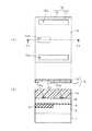
図27〜33は、従来の半導体装置の製造方法を工程順に示す図である。図27(A)〜33(A)は上面図であり、図27(B)〜33(B)は、図27(A)〜33(A)中に示した線分X100−X100に沿った位置に関する断面構造を示す断面図である。
【0003】
図27を参照して、まず、シリコン基板101の上面内に不純物を導入することにより、ウェル102を形成する。このとき、リン等のp型不純物が導入された場合はpウェルが形成され、ボロン等のn型不純物が導入された場合はnウェルが形成される。次に、周知のトレンチ分離技術によって、シリコン酸化膜等から成るトレンチ型の素子分離絶縁膜103を、シリコン基板101の上面内に部分的に形成する。図27(A)を参照して、素子分離絶縁膜103が形成されていない部分が、MOSFETを形成するための素子形成領域となる。即ち、素子形成領域は、素子分離絶縁膜103によって規定される。
【0004】
図28を参照して、次に、TEOS(Tetra Etyle Ortho Silicate)を原料ガスに用いたCVD法によって、シリコン酸化膜104を、ウェル102及び素子分離絶縁膜103上に全面的に形成する。次に、CVD法によって、ポリシリコン膜105を、シリコン酸化膜104上に全面的に形成する。次に、熱酸化法あるいはTEOSを原料ガスに用いたCVD法によって、シリコン酸化膜106を、ポリシリコン膜105上に全面的に形成する。次に、ネガ型のフォトレジスト107を、シリコン酸化膜106上に全面的に塗布する。
【0005】
図29を参照して、次に、ゲート電極が形成される予定の領域(形成予定領域)の上方に開口部111(図面では符号111i〜111kを付している)が形成されたパターンを有するフォトマスク110を用いて、換言すれば、ゲート電極のレイアウトパターンと同様の開口パターンを有するフォトマスク110を用いて、フォトレジスト107を露光する。フォトマスク110は、ガラス基板108上に遮光膜109が形成された構造を有している。図29(A)を参照して、フォトマスク110には、複数(ここでは、例として3個としている)の開口部111i〜111kが形成されている。開口部111iと開口部111jとは、ゲート幅方向(紙面の上下方向)に沿う同一直線上で、互いに隣接して形成されている。
【0006】
図30には、図29に示した工程で露光された後のフォトレジスト107の状態を示している。図30(A)を参照して、フォトレジスト107には、フォトマスク110の開口部111に対応して、露光部112(図面では符号112i〜112kを付している)が形成されている。
【0007】
図31を参照して、次に、図29に示した工程で露光されなかった部分(非露光部分)のフォトレジスト107、即ち、露光部112以外の部分のフォトレジスト107を、現像によって除去する。これにより、シリコン酸化膜106上には、露光部112に対応するフォトレジスト113(図面では符号113i〜113kを付している)のみが残る。
【0008】
図32を参照して、次に、フォトレジスト113を用いてシリコン酸化膜106をパターニングする。具体的には、フォトレジスト113をエッチングマスクに用いて、シリコン基板101の深さ方向にエッチングレートの高い異方性ドライエッチング法によって、シリコン酸化膜106をエッチングする。これにより、フォトレジスト113によって覆われていない部分のシリコン酸化膜106が除去され、その部分の下方におけるポリシリコン膜105の上面が露出する。ポリシリコン膜105上には、全面的に形成されていたシリコン酸化膜106のうち、フォトレジスト113によって覆われていた部分のシリコン酸化膜114(図面では符号114i〜114kを付している)のみが残る。その後、フォトレジスト113を除去する。
【0009】
図33を参照して、次に、シリコン酸化膜114をエッチングマスク(ハードマスク)に用いて、シリコン基板101の深さ方向にエッチングレートの高い異方性ドライエッチング法によって、ポリシリコン膜105及びシリコン酸化膜104をこの順にエッチングする。これにより、シリコン酸化膜114によって覆われていない部分のポリシリコン膜105及びシリコン酸化膜104が除去され、その部分の下方におけるウェル102及び素子分離絶縁膜103の上面が露出する。図33(B)を参照して、ウェル102上には、シリコン酸化膜116k、ポリシリコン膜115k、及びシリコン酸化膜114kがこの順に積層された構造を有するゲート構造117(図面では符号117kを付している)が形成されている。シリコン酸化膜116kはゲート絶縁膜として機能し、ポリシリコン膜115kはゲート電極として機能する。図33(A)を参照して、ウェル102及び素子分離絶縁膜103上には、ゲート構造117kと同様の積層構造を有するゲート構造117i,117jが形成されている。
【0010】
その後、CVD法によってシリコン酸化膜を全面に形成した後、該シリコン酸化膜を異方性エッチング法によってエッチバックすることにより、ゲート構造117の側面にサイドウォールを形成する。次に、イオン注入法によってウェル102の上面内に不純物を導入することにより、ゲート構造117を挟んで対を成すソース・ドレイン領域を形成する。以上の工程により、MOSFETが形成される。その後、配線工程に引き続き、半導体装置が完成する。
【0011】
【発明が解決しようとする課題】
このように従来の半導体装置の製造方法では、図29に示した工程で、ゲート電極のレイアウトパターンと同様の開口パターンを有するフォトマスク110を用いて、フォトレジスト107を露光する。そして、フォトレジスト107を現像してフォトレジスト113を得た後、フォトレジスト113を用いてシリコン酸化膜106をパターニングすることによりシリコン酸化膜114を形成し、さらに、シリコン酸化膜114をハードマスクに用いてエッチングを行うことにより、ゲート構造117を形成する。
【0012】
しかしながら、図29に示した工程でフォトレジスト107を露光する際、開口部111の角部は光の干渉の影響を受けるため、図30に示したように、露光部112は角部が丸まった形状になる。従って、半導体装置の微細化に伴ってゲート長方向(紙面の左右方向)に関する開口部111の寸法が短くなると、ゲート幅方向に関する露光部112の寸法は、開口部111の寸法よりも小さくなる。露光部112の形状は最終的にゲート構造117の形状に反映するため、ゲート幅方向に関して、ゲート構造117の仕上がり寸法が、開口部111の寸法よりも小さくなる。即ち、従来の半導体装置の製造方法によると、ゲート電極のレイアウトパターンと同様の開口パターンを有する一枚のフォトマスク110を用いてフォトレジスト107が露光されることに起因して、ゲート幅方向に関して、ゲート構造117の仕上がり形状が、フォトマスク110が有する開口部111の形状よりも後退するという問題があった。かかる問題は、ゲート構造117の仕上がり形状のばらつきに起因してMOSFETの性能を劣化させたり、半導体集積回路の高集積化を妨げることにもなる。
【0013】
かかる問題を解決するために、ゲート構造117の後退量を予測して、ゲート幅方向に関する開口部111の寸法を若干広く設計しておく手法も考えられる。しかし、後退量を予測するためには、実験を繰り返し行う必要がある。また、図29に示したように、開口部111iと開口部111jとがゲート幅方向に互いに隣接する場合には、開口部111i,111jの幅を拡げる量にも限界がある。従って、この手法は、従来の半導体装置の製造方法における問題を解決するための、根本的な解決策とはならない。
【0014】
この発明はかかる問題を解決するために成されたものであり、フォトマスクの開口部の形状よりもゲート構造の形状が後退することを回避することにより、設計寸法通りにゲート構造を形成し得る半導体装置の製造方法を得ることを目的とするものである。
【0015】
【課題を解決するための手段】
この発明のうち請求項1に係る半導体装置の製造方法は、(a)半導体基板を準備する工程と、(b)半導体基板上に、導電性の第1の膜を形成する工程と、(c)第1の膜上に第2の膜を形成する工程と、(d)第2の膜上に第1のフォトレジストを形成する工程と、(e)第1のパターンを有する第1のフォトマスクを用いて、第1のフォトレジストを露光する工程と、(f)工程(e)によって露光された後の第1のフォトレジストを現像する工程と、(g)工程(f)によって現像された後の第1のフォトレジストを用いて第2の膜をパターニングすることにより、ゲート電極の形成予定領域の上方に、ゲート電極のゲート幅よりも幅広の第3の膜を形成し、しかる後に、前記第1のフォトレジストを除去する工程と、(h)工程(g)よりも後に実行され、第3の膜を覆って第1の膜上に第2のフォトレジストを形成する工程と、(i)ゲート電極のゲート幅方向の端部を規定する第2のパターンを有する第2のフォトマスクを用いて、第2のフォトレジストを露光する工程と、(j)工程(i)によって露光された後の第2のフォトレジストを現像する工程と、(k)工程(j)によって現像された後の第2のフォトレジストを用いて第3の膜をパターニングすることにより、第4の膜を形成する工程と、(l)第4の膜をエッチングマスクに用いて第1の膜をエッチングすることにより、ゲート電極を形成する工程とを備え、(m)前記工程(g)よりも後に実行され、エッチングによって前記第3の膜を細らせる工程をさらに備え、前記工程(m)は、前記工程(h)よりも前に実行され、ゲート電極はメモリセルのゲート電極であるものである。
【0016】
また、この発明のうち請求項2に記載の半導体装置の製造方法は、(a)半導体基板を準備する工程と、(b)半導体基板上に、導電性の第1の膜を形成する工程と、(c)第1の膜上に第2の膜を形成する工程と、(d)第2の膜上に第1のフォトレジストを形成する工程と、(e)第1のパターンを有する第1のフォトマスクを用いて、第1のフォトレジストを露光する工程と、(f)工程(e)によって露光された後の第1のフォトレジストを現像する工程と、(g)工程(f)によって現像された後の第1のフォトレジストを用いて第2の膜をパターニングすることにより、第1のゲート電極の形成予定領域の上方から、ゲート幅方向に沿って第1のゲート電極に隣接する第2のゲート電極の形成予定領域の上方に繋がって延在する第3の膜を形成し、しかる後に、前記第1のフォトレジストを除去する工程と、(h)工程(g)よりも後に実行され、第3の膜を覆って第1の膜上に第2のフォトレジストを形成する工程と、(i)第2のゲート電極側の第1のゲート電極の端部、及び第1のゲート電極側の第2のゲート電極の端部を規定する第2のパターンを有する第2のフォトマスクを用いて、第2のフォトレジストを露光する工程と、(j)工程(i)によって露光された後の第2のフォトレジストを現像する工程と、(k)工程(j)によって現像された後の第2のフォトレジストを用いて第3の膜をパターニングすることにより、第4の膜を形成する工程と、(l)第4の膜をエッチングマスクに用いて第1の膜をエッチングすることにより、第1及び第2のゲート電極を形成する工程とを備え、(m)前記工程(g)よりも後に実行され、エッチングによって前記第3の膜を細らせる工程をさらに備え、前記工程(m)は、前記工程(h)よりも前に実行され、第1および第2のゲート電極はメモリセルのゲート電極であるものである。
【0017】
また、この発明のうち請求項3に記載の半導体装置の製造方法は、請求項1又は2に記載の半導体装置の製造方法であって、前記(g)工程によって、前記第3の膜は複数形成され、前記メモリセルは第一SRAMメモリセルであり、前記第一SRAMメモリセルは平面視において、前記ゲート幅方向に延びる直線状の第一ライン上にゲート電極が延び、NMOSで構成された第一ドライバトランジスタと、前記第一ライン上にゲート電極が延び、PMOSで構成された第一負荷トランジスタと、前記第一ライン上にゲート電極が延び、NMOSで構成された第一アクセストランジスタと、前記第一ラインと平行な直線状の第二ライン上にゲート電極が延び、NMOSで構成された第二アクセストランジスタと、前記第二ライン上にゲート電極が延び、PMOSで構成された第二負荷トランジスタと、前記第二ライン上にゲート電極が延び、NMOSで構成された第二ドライバトランジスタとを有するように構成され、前記第一ラインと前記第二ラインはゲート長方向にて隣り合い、前記第一ドライバトランジスタと前記第一負荷トランジスタとは互いにゲート電極を共有し、前記第二負荷トランジスタと前記第二ドライバトランジスタとは互いにゲート電極を共有し、前記第一SRAMメモリセルと前記ゲート幅方向にて隣り合う第二SRAMメモリセルと前記第二アクセストランジスタとは互いにゲート電極を共有し、前記第二SRAMメモリセルの反対側に前記第一SRAMメモリセルと前記ゲート幅方向にて隣り合う第三SRAMメモリセルと前記第一アクセストランジスタとは互いにゲート電極を共有し、前記工程(k)によって、前記ゲート幅方向に第一の所定の間隔を隔てつつ前記第一負荷トランジスタのゲート電極と前記第一アクセストランジスタのゲート電極とが互いに隣り合うように、前記第4の膜がパターニングされ、前記工程(k)によって、前記ゲート幅方向に前記第一の所定の間隔を隔てつつ前記第二アクセストランジスタのゲート電極と前記第二負荷トランジスタのゲート電極とが互いに隣り合うように、前記第4の膜がパターニングされ、前記工程(k)によって、前記ゲート幅方向に前記第一の所定の間隔を隔てつつ前記第二SRAMメモリセルのゲート電極と前記第一ドライバトランジスタのゲート電極とが互いに隣り合うように、前記第4の膜がパターニングされ、前記工程(k)によって、前記ゲート幅方向に前記第一の所定の間隔を隔てつつ前記第三SRAMメモリセルのゲート電極と前記第二ドライバトランジスタのゲート電極とが互いに隣り合うように、前記第4の膜がパターニングされる。
【0018】
また、この発明のうち請求項4に記載の半導体装置の製造方法は、請求項3に記載の半導体装置の製造方法であって、前記ゲート長方向に第二の所定の間隔を隔てて、前記第一ドライバトランジスタ及び前記第二アクセストランジスタのゲート電極が互いに隣り合うように配置され、前記ゲート長方向に前記第二の所定の間隔を隔てて、前記第一負荷トランジスタ及び前記第二負荷トランジスタのゲート電極が互いに隣り合うように配置され、前記ゲート長方向に前記第二の所定の間隔を隔てて、前記第一アクセストランジスタ及び前記第二ドライバトランジスタのゲート電極が互いに隣り合うように配置される。
【0019】
また、この発明のうち請求項5に記載の半導体装置の製造方法は、請求項1〜4のいずれか一つに記載の半導体装置の製造方法が、SRAMメモリセルを構成する複数のトランジスタがそれぞれ有するゲート電極の形成に適用されることを特徴とするものである。
【0020】
また、この発明のうち請求項6に記載の半導体装置の製造方法は、請求項1〜4のいずれか一つに記載の半導体装置の製造方法が、メモリセルアレイ内に形成される複数のメモリセルトランジスタがそれぞれ有するゲート電極の形成に適用されることを特徴とするものである。
【0021】
また、この発明のうち請求項7に記載の半導体装置の製造方法は、(a)半導体基板を準備する工程と、(b)半導体基板上に、導電性の第1の膜を形成する工程と、(c)第1の膜上に第2の膜を形成する工程と、(d)第2の膜上の第1のフォトレジストを、第一のパターンにパターニングする工程と、(e)第一のパターンを用いて第2の膜をパターニングすることにより、第二のパターンを形成し、しかる後に、前記第1のフォトレジストを除去する工程と、(f)工程(e)よりも後に実行され、第1の膜上に第二のパターンを覆うように形成される第2のフォトレジストを、第二のパターンを複数に分割するような開口部を有する第三のパターンに加工する工程と、(g)第三のパターンを用いて第二のパターンをパターニングすることにより、複数の第四のパターンを形成する工程と、(h)複数の第四のパターンをエッチングマスクに用いて第1の膜をエッチングすることにより、複数のゲート電極を形成する工程と、(i)前記工程(e)よりも後に実行され、前記第二のパターンを等方性エッチングによってパターンを細らせる工程とを、備え、前記工程(i)は、前記工程(f)よりも前に実行され、前記複数のゲート電極それぞれはメモリセルに用いられ、第一のパターンは複数のゲート電極それぞれのゲート幅方向に延びるパターンである。
また、この発明のうち請求項8に記載の半導体装置の製造方法は、請求項7に記載の半導体装置の製造方法であって、開口部は複数のゲート電極それぞれのゲート長方向に延びることを特徴とするものである。
また、この発明のうち請求項9に記載の半導体装置の製造方法は、請求項7に記載の半導体装置の製造方法であって、前記(e)工程によって、前記第二のパターンは複数形成され、前記メモリセルは第一SRAMメモリセルであり、前記第一SRAMメモリセルは平面視において、前記ゲート幅方向に延びる直線状の第一ライン上にゲート電極が延び、NMOSで構成された第一ドライバトランジスタと、前記第一ライン上にゲート電極が延び、PMOSで構成された第一負荷トランジスタと、前記第一ライン上にゲート電極が延び、NMOSで構成された第一アクセストランジスタと、前記第一ラインと平行な直線状の第二ライン上にゲート電極が延び、NMOSで構成された第二アクセストランジスタと、前記第二ライン上にゲート電極が延び、PMOSで構成された第二負荷トランジスタと、前記第二ライン上にゲート電極が延び、NMOSで構成された第二ドライバトランジスタとを有するように構成され、前記第一ラインと前記第二ラインはゲート長方向にて隣り合い、前記第一ドライバトランジスタと前記第一負荷トランジスタとは互いにゲート電極を共有し、前記第二負荷トランジスタと前記第二ドライバトランジスタとは互いにゲート電極を共有し、前記第一SRAMメモリセルと前記ゲート幅方向にて隣り合う第二SRAMメモリセルと前記第二アクセストランジスタとは互いにゲート電極を共有し、前記第二SRAMメモリセルの反対側に前記第一SRAMメモリセルと前記ゲート幅方向にて隣り合う第三SRAMメモリセルと前記第一アクセストランジスタとは互いにゲート電極を共有し、前記工程(g)によって、前記ゲート幅方向に第一の所定の間隔を隔てつつ前記第一負荷トランジスタのゲート電極と前記第一アクセストランジスタのゲート電極とが互いに隣り合うように、前記第4の膜がパターニングされ、前記工程(g)によって、前記ゲート幅方向に前記第一の所定の間隔を隔てつつ前記第二アクセストランジスタのゲート電極と前記第二負荷トランジスタのゲート電極とが互いに隣り合うように、前記第4の膜がパターニングされ、前記工程(g)によって、前記ゲート幅方向に前記第一の所定の間隔を隔てつつ前記第二SRAMメモリセルのゲート電極と前記第一ドライバトランジスタのゲート電極とが互いに隣り合うように、前記第4の膜がパターニングされ、前記工程(g)によって、前記ゲート幅方向に前記第一の所定の間隔を隔てつつ前記第三SRAMメモリセルのゲート電極と前記第二ドライバトランジスタのゲート電極とが互いに隣り合うように、前記第4の膜がパターニングされる。
また、この発明のうち請求項10に記載の半導体装置の製造方法は、請求項9に記載の半導体装置の製造方法であって、前記ゲート長方向に第二の所定の間隔を隔てて、前記第一ドライバトランジスタ及び前記第二アクセストランジスタのゲート電極が互いに隣り合うように配置され、前記ゲート長方向に前記第二の所定の間隔を隔てて、前記第一負荷トランジスタ及び前記第二負荷トランジスタのゲート電極が互いに隣り合うように配置され、前記ゲート長方向に前記第二の所定の間隔を隔てて、前記第一アクセストランジスタ及び前記第二ドライバトランジスタのゲート電極が互いに隣り合うように配置される。
また、この発明のうち請求項11に記載の半導体装置の製造方法は、請求項7に記載の半導体装置の製造方法であって、SRAMメモリセルを構成する複数のトランジスタがそれぞれ有するゲート電極の形成に適用されることを特徴とするものである。
また、この発明のうち請求項12に記載の半導体装置の製造方法は、請求項7に記載の半導体装置の製造方法であって、メモリセルアレイ内に形成される複数のメモリセルトランジスタがそれぞれ有するゲート電極の形成に適用されることを特徴とするものである。
また、この発明のうち請求項13に記載の半導体装置の製造方法は、請求項7に記載の半導体装置の製造方法であって、等方性エッチングはフッ酸を用いたウエットエッチングであることを特徴とするものである。
また、この発明のうち請求項14に記載の半導体装置の製造方法は、請求項1又は2に記載の半導体装置の製造方法であって、前記工程(m)は等方性エッチングにより前記第3の膜を細らせる工程である。
また、この発明のうち請求項15に記載の半導体装置の製造方法は、請求項14に記載の半導体装置の製造方法であって、前記等方性エッチングはフッ酸を用いたウエットエッチングである。
【0022】
【発明の実施の形態】
実施の形態1.
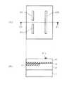
図1〜13は、本発明の実施の形態1に係る半導体装置の製造方法を工程順に示す図である。図1(A)〜13(A)は上面図であり、図1(B)〜13(B)は、図1(A)〜13(A)中に示した線分X1−X1に沿った位置に関する断面構造を示す断面図である。
【0023】
図1を参照して、まず、シリコン基板1の上面内に不純物を導入することにより、ウェル2を形成する。このとき、リン等のp型不純物が導入された場合はpウェルが形成され、ボロン等のn型不純物が導入された場合はnウェルが形成される。次に、周知のトレンチ分離技術によって、シリコン酸化膜等から成るトレンチ型の素子分離絶縁膜3を、シリコン基板1の上面内に部分的に形成する。図1(A)を参照して、素子分離絶縁膜3が形成されていない部分が、MOSFETを形成するための素子形成領域となる。即ち、素子形成領域は、素子分離絶縁膜3によって規定される。
【0024】
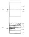
図2を参照して、次に、TEOSを原料ガスに用いたCVD法によって、シリコン酸化膜4を、ウェル2及び素子分離絶縁膜3上に全面的に形成する。次に、CVD法によって、ポリシリコン膜5を、シリコン酸化膜4上に全面的に形成する。次に、熱酸化法あるいはTEOSを原料ガスに用いたCVD法によって、シリコン酸化膜6を、ポリシリコン膜5上に全面的に形成する。次に、ポジ型のフォトレジスト7を、シリコン酸化膜6上に全面的に塗布する。なお、シリコン酸化膜4,6を形成する代わりに、シリコン酸窒化膜(SiON)や強誘電体膜(TiO2、Ta2O5等)等の他の絶縁膜を形成してもよい。
【0025】
図3を参照して、次に、所定の遮光パターンを有するフォトマスク10を用いて、フォトレジスト7を露光する。フォトマスク10は、ガラス基板8上に複数(ここでは、例として2個としている)の遮光膜9a,9bが形成された構造を有しているが、遮光膜9a,9bの形状は、ゲート構造の最終的な形状とは一致しない。
【0026】
最終的なMOSFETの構造は、図13に示されている。図3(A)と図13(A)とを比較して、ゲート長方向(紙面の左右方向)に関する遮光膜9a,9bの寸法は、ゲート構造25i〜25kのゲート長に等しい。また、遮光膜9bは、ゲート構造25kの形成予定領域の上方に形成されており、ゲート幅方向(紙面の上下方向)に関する遮光膜9bの寸法は、ゲート構造25kのゲート幅よりも広い。即ち、遮光膜9bは、ゲート幅方向に関するゲート構造25kの両端部よりも外側に延びて形成されている。また、遮光膜9aは、ゲート構造25i,25jの上方に形成されており、ゲート構造25iの形成予定領域の上方からゲート構造25jの形成予定領域の上方に繋がって延在している。しかも遮光膜9aは、ゲート幅方向に関するゲート構造25i,25jの両端部よりも外側に延びて形成されている。なお、図13(A)を参照して、ゲート構造25iとゲート構造25jとは、ゲート幅方向に沿う同一直線上で、互いに隣接して形成されている。
【0027】
図4には、図3に示した工程で露光された後のフォトレジスト7の状態を示している。図4(A)を参照して、フォトレジスト7には、フォトマスク10の遮光膜9a,9bに対応して、非露光部12a,12bが形成されている。フォトレジスト7のうち非露光部12a,12b以外の部分は、露光部11となる。ここで、図3に示した工程でフォトレジスト7を露光する際、遮光膜9a,9bの角部は光の干渉の影響を受けるため、図4(A)に示すように、非露光部12a,12bは、角部が丸まった形状になる。
【0028】
図5を参照して、次に、現像によって、フォトレジスト7の露光部11を除去する。これにより、シリコン酸化膜6上には、非露光部12a,12bに対応するフォトレジスト13a,13bのみが残る。
【0029】
図6を参照して、次に、フォトレジスト13a,13bを用いてシリコン酸化膜6をパターニングする。具体的には、フォトレジスト13a,13bをエッチングマスクに用いて、シリコン基板1の深さ方向にエッチングレートの高い異方性ドライエッチング法によって、シリコン酸化膜6をエッチングする。これにより、フォトレジスト13a,13bによって覆われていない部分のシリコン酸化膜6が除去され、その部分の下方におけるポリシリコン膜5の上面が露出する。ポリシリコン膜5上には、全面的に形成されていたシリコン酸化膜6のうち、フォトレジスト13a,13bによって覆われていた部分のシリコン酸化膜14a,14bのみが残る。その後、フォトレジスト13a,13bを除去する。
【0030】
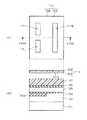
図7を参照して、次に、ポジ型のフォトレジスト15を、シリコン酸化膜14a,14bを覆ってポリシリコン膜5上に全面的に塗布する。図8を参照して、次に、所定の開口パターンを有するフォトマスク18を用いて、フォトレジスト15を露光する。フォトマスク18は、ガラス基板16上に遮光膜17が形成された構造を有している。図8(A)を参照して、フォトマスク18には、複数(ここでは、例として3個としている)の開口部19(図面では符号19s〜19uを付している)が形成されている。開口部19の形状は、ゲート構造の最終的な形状とは一致しない。
【0031】
図8(A)と図13(A)とを比較して、ゲート幅方向に関するゲート構造25i,25kの各上端部は、開口部19sの下辺によって規定されている。また、ゲート構造25j,25kの各下端部は、開口部19uの上辺によって規定されている。また、ゲート構造25iの下端部及びゲート構造25jの上端部は、開口部19tの上辺及び下辺によってそれぞれ規定されている。即ち、フォトマスク18は、ゲート幅方向に関するゲート構造25i〜25jの各端部を規定するための開口パターンを有するフォトマスクである。
【0032】
図9には、図8に示した工程で露光された後のフォトレジスト15の状態を示している。図9(A)を参照して、フォトレジスト15には、フォトマスク18の開口部19に対応して、露光部20(図面では符号20s〜20uを付している)が形成されている。ここで、図8に示した工程でフォトレジスト15を露光する際、開口部19の角部は光の干渉の影響を受けるため、図9(A)に示すように、露光部20は、角部が丸まった形状になる。
【0033】
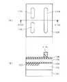
図10を参照して、次に、現像によって、フォトレジスト15の露光部20を除去する。これにより、各露光部20s〜20uに対応して、フォトレジスト15内に開口部21s〜21uがそれぞれ形成される。開口部21s内には、シリコン酸化膜14a,14bの各上端部が露出している。また、開口部21u内には、シリコン酸化膜14a,14bの各下端部が露出している。また、開口部21t内には、シリコン酸化膜14aの中央部が露出している。
【0034】
図11を参照して、次に、フォトレジスト15をエッチングマスクに用いて、開口部21s〜21u内に露出している部分のシリコン酸化膜14a,14bを、エッチングによって除去する。フォトレジスト15によって覆われている部分のシリコン酸化膜14a,14bは、このときのエッチングによっては除去されず、シリコン酸化膜22(図面では符号22i〜22kを付している)として残る。
【0035】
図12を参照して、次に、フォトレジスト15を除去する。ポリシリコン膜5上には、ゲート構造25i〜25kの形成予定領域の上方にシリコン酸化膜22i〜22kが形成されている。
【0036】
図13を参照して、次に、シリコン酸化膜22をエッチングマスク(ハードマスク)に用いて、シリコン基板1の深さ方向にエッチングレートの高い異方性ドライエッチング法によって、ポリシリコン膜5及びシリコン酸化膜4をこの順にエッチングする。これにより、シリコン酸化膜22によって覆われていない部分のポリシリコン膜5及びシリコン酸化膜4が除去され、その部分の下方におけるウェル2及び素子分離絶縁膜3の上面が露出する。
【0037】
図13(B)を参照して、ウェル2上には、シリコン酸化膜24k、ポリシリコン膜23k、及びシリコン酸化膜22kがこの順に積層された構造を有するゲート構造25(図面では符号25kを付している)が形成されている。シリコン酸化膜24kはゲート絶縁膜として機能し、ポリシリコン膜23kはゲート電極として機能する。図13(A)を参照して、ウェル2及び素子分離絶縁膜3上には、ゲート構造25kと同様の積層構造を有するゲート構造25i,25jが形成されている。
【0038】
その後、CVD法によってシリコン酸化膜を全面に形成した後、該シリコン酸化膜を異方性エッチング法によってエッチバックすることにより、ゲート構造25の側面にサイドウォールを形成する。次に、イオン注入法によってウェル2の上面内に不純物を導入することにより、ゲート構造25を挟んで対を成すソース・ドレイン領域を形成する。以上の工程により、MOSFETが形成される。その後、配線工程に引き続き、半導体装置が完成する。
【0039】
なお、以上の説明では、図3に示した工程でフォトレジスト7を露光した後に、フォトレジスト7の現像(図5)及びシリコン酸化膜6のエッチング(図6)を行い、その後、図8に示した工程でフォトレジスト15を露光した後に、フォトレジスト15の現像(図10)及びシリコン酸化膜14a,14bのエッチング(図11)を行った。しかし、フォトマスク10を用いてフォトレジスト7を露光した後に、続けてフォトマスク18を用いてフォトレジスト7を露光し、その後、フォトレジスト7の現像及びシリコン酸化膜6のエッチングを一括して行ってもよい。かかる方法によっても、図12に示した構造と同様の構造のシリコン酸化膜22を形成することができる。
【0040】
このように本実施の形態1に係る半導体装置の製造方法によれば、ゲート構造25kのゲート幅よりも幅広のシリコン酸化膜14bを形成した後、シリコン酸化膜14bの端部を除去することによって、シリコン酸化膜22kを形成する。そして、シリコン酸化膜22kをハードマスクに用いたエッチングによって、ゲート構造25kを形成する。従って、ゲート構造25kのゲート幅を、フォトマスク18における開口部19sの下辺と開口部19uの上辺との間隔に、正確に設定することができる。
【0041】
また、ゲート構造25iの形成予定領域の上方からゲート構造25jの形成予定領域の上方に繋がって延在するシリコン酸化膜14aを形成した後、シリコン酸化膜14aの中央部を除去することによって、シリコン酸化膜22iとシリコン酸化膜22jとに分離する。そして、シリコン酸化膜22i,22jをハードマスクに用いたエッチングによって、ゲート構造25i,25jを形成する。従って、ゲート構造25iとゲート構造25jとの間隔を、フォトマスク18における開口部21tの上辺と下辺との間隔(最小線幅)に設定できる。その結果、半導体集積回路の高集積化を図ることができる。
【0042】
なお、特開平9−289153号公報には、光の干渉に起因するゲート電極の先端部の後退を抑制するために、(A)シリコン基板上にゲート酸化膜及びゲート電極をこの順に形成する工程と、(B)ゲート電極上に第1のフォトレジストを形成する工程と、(C)第1のフォトマスクを用いて第1のフォトレジストを露光する工程と、(D)第1のフォトレジストを現像する工程と、(E)現像後の第1のフォトレジストをエッチングマスクに用いてゲート電極をエッチングする工程と、(F)第2のフォトレジストを形成する工程と、(G)第2のフォトマスクを用いて第2のフォトレジストを露光する工程と、(H)第2のフォトレジストを現像する工程と、(I)現像後の第2のフォトレジストをエッチングマスクに用いてゲート電極をエッチングする工程とが、この順に実行される半導体装置の製造方法が記載されている。
【0043】
かかる方法では、工程(E)及び工程(I)でゲート電極がエッチングされるが、これら2回のエッチングにおける各オーバーエッチによって、シリコン基板はそれぞれダメージを受ける。これに対して本実施の形態1に係る半導体装置の製造方法では、シリコン基板1がダメージを受けるのは、図13に示した工程でのエッチングにおけるオーバーエッチのみである。従って、本実施の形態1に係る半導体装置の製造方法は、上記公報に記載された半導体装置の製造方法と比較して、シリコン基板が受けるダメージを低減できるという優れた効果を有している。
【0044】
実施の形態2.
図14〜21は、本発明の実施の形態2に係る半導体装置の製造方法を工程順に示す図である。図14(A)〜21(A)は上面図であり、図14(B)〜21(B)は、図14(A)〜21(A)中に示した線分X1−X1に沿った位置に関する断面構造を示す断面図である。
【0045】
まず、上記実施の形態1に係る半導体装置の製造方法と同様の工程を経て、図6に示した構造を得る。図14を参照して、次に、等方性エッチング法、例えば、フッ酸を用いたウェットエッチング法によって、シリコン酸化膜14a,14bの全体を所定量だけエッチングし、これにより、シリコン酸化膜14a,14bを細らせてシリコン酸化膜30a,30bを形成する。
【0046】
図15を参照して、次に、フォトレジスト15を、シリコン酸化膜30a,30bを覆ってポリシリコン膜5上に全面的に塗布する。図16を参照して、次に、フォトマスク18を用いて、フォトレジスト15を露光する。図17には、図16に示した工程で露光された後のフォトレジスト15の状態を示している。
【0047】
図18を参照して、次に、現像によって、フォトレジスト15の露光部20を除去する。これにより、フォトレジスト15内に開口部21s〜21uが形成される。開口部21s内には、シリコン酸化膜30a,30bの各上端部が露出している。また、開口部21u内には、シリコン酸化膜30a,30bの各下端部が露出している。また、開口部21t内には、シリコン酸化膜30aの中央部が露出している。
【0048】
図19を参照して、次に、フォトレジスト15をエッチングマスクに用いて、開口部21s〜21u内に露出している部分のシリコン酸化膜30a,30bを、エッチングによって除去する。フォトレジスト15によって覆われている部分のシリコン酸化膜30a,30bは、このときのエッチングによっては除去されず、シリコン酸化膜31(図面中では符号31i〜31kを付している)として残る。
【0049】
図20を参照して、次に、フォトレジスト15を除去する。図21を参照して、次に、シリコン酸化膜31kをエッチングマスク(ハードマスク)に用いて、シリコン基板1の深さ方向にエッチングレートの高い異方性ドライエッチング法によって、ポリシリコン膜5及びシリコン酸化膜4をこの順にエッチングする。これにより、シリコン酸化膜31kによって覆われていない部分のポリシリコン膜5及びシリコン酸化膜4が除去され、その部分の下方におけるウェル2及び素子分離絶縁膜3の上面が露出する。図21(B)を参照して、ウェル2上には、シリコン酸化膜34k、ポリシリコン膜33k、及びシリコン酸化膜31kがこの順に積層された構造を有するゲート構造35(図面では符号35kを付している)が形成されている。シリコン酸化膜34kはゲート絶縁膜として機能し、ポリシリコン膜33kはゲート電極として機能する。図21(A)を参照して、ウェル2及び素子分離絶縁膜3上には、ゲート構造35kと同様の積層構造を有するゲート構造35i,35jが形成されている。
【0050】
その後、ゲート構造35の側面にサイドウォールを形成した後、ウェル2の上面内にソース・ドレイン領域を形成する。以上の工程により、MOSFETが形成される。その後、配線工程に引き続き、半導体装置が完成する。
【0051】
このように本実施の形態2に係る半導体装置の製造方法によれば、図14に示した工程でシリコン酸化膜14a,14bを細らせる。従って、最終的に得られるゲート構造35のゲート長が短くなるため、上記実施の形態1に係る半導体装置の製造方法によって得られるMOSFETと比較すると、動作の高速化を図ることができる。
【0052】
しかも、シリコン酸化膜14a,14bを細らせる工程(図14)は、シリコン酸化膜31の端部を規定するためのエッチング工程(図19)よりも前に実行される。従って、シリコン酸化膜14a,14bを細らせるための等方性エッチングによってシリコン酸化膜31の端部がエッチングされてゲート幅が変動することや、シリコン酸化膜31iとシリコン酸化膜31jとの間隔が広がって高集積化の妨げになることを、適切に回避することができる。
【0053】
実施の形態3.
本実施の形態3は、上記実施の形態1,2に係る半導体装置の製造方法を、SRAMメモリセルを構成する複数のトランジスタがそれぞれ有するゲート電極の形成に適用したものである。図22は、本実施の形態3に係るSRAMメモリセルのレイアウト構成を示す上面図である。かかるレイアウト構成は、例えば特開平10−178110号公報に記載されているので、詳細な説明は省略する。
【0054】
まず、シリコン基板上にゲート絶縁膜及びポリシリコン膜をこの順に全面的に形成した後、ポリシリコン膜上にシリコン酸化膜を全面的に形成する。次に、第1のフォトマスクを用いた写真製版法及び異方性ドライエッチング法によって、シリコン酸化膜をパターニングする。これにより、ドライバトランジスタN1、負荷トランジスタP1、及びアクセストランジスタN4の各ゲート電極の形成予定領域の上方に、図中の破線部分を含む直線状のシリコン酸化膜が形成されるとともに、ドライバトランジスタN2、負荷トランジスタP2、及びアクセストランジスタN3の各ゲート電極の形成予定領域の上方に、図中の破線部分を含む直線状のシリコン酸化膜が形成される。以上の工程は、上記実施の形態1に係る半導体装置の製造方法における、図6に示した工程までの工程に相当する。
【0055】
次に、第2のフォトマスクを用いた写真製版法及び異方性ドライエッチング法によって、図中の破線部分のシリコン酸化膜を除去する。以上の工程は、上記実施の形態1に係る半導体装置の製造方法における、図12に示した工程までの工程に相当する。
【0056】
次に、残ったシリコン酸化膜をハードマスクに用いてポリシリコン膜をエッチングすることにより、上記各種トランジスタのゲート電極を形成する。かかる工程は、上記実施の形態1に係る半導体装置の製造方法における、図13に示した工程に相当する。
【0057】
このように、本実施の形態3に係る半導体装置の製造方法によれば、上記実施の形態1,2に係る半導体装置の製造方法を、SRAMメモリセルを構成する複数のトランジスタがそれぞれ有するゲート電極の形成に適用する。これにより、アクセストランジスタN4のゲート電極と負荷トランジスタP1のゲート電極との間隔、アクセストランジスタN3のゲート電極と負荷トランジスタP2のゲート電極との間隔、及び互いに隣接するドライバトランジスタのゲート電極同士の間隔を、いずれも最小線幅にすることができる。そのため、セルサイズの縮小化を図ることができる。
【0058】
実施の形態4.
本実施の形態4は、上記実施の形態1,2に係る半導体装置の製造方法を、図22とは異なるSRAMメモリセルにおけるゲート電極の形成に適用したものである。図23は、本実施の形態4に係るSRAMメモリセルのレイアウト構成を示す上面図である。かかるレイアウト構成は、例えば特開2000−36543号公報に記載されているので、詳細な説明は省略する。
【0059】
まず、シリコン基板上にゲート絶縁膜及びポリシリコン膜をこの順に全面的に形成した後、ポリシリコン膜上にシリコン酸化膜を全面に形成する。次に、第1のフォトマスクを用いた写真製版法及び異方性ドライエッチング法によって、シリコン酸化膜をパターニングする。これにより、ドライバトランジスタN1及び負荷トランジスタP1の各ゲート電極の形成予定領域の上方に、図中の破線部分を含む直線状のシリコン酸化膜が形成されるとともに、ドライバトランジスタN2及び負荷トランジスタP2の各ゲート電極の形成予定領域の上方に、図中の破線部分を含む直線状のシリコン酸化膜が形成される。以上の工程は、上記実施の形態1に係る半導体装置の製造方法における、図6に示した工程までの工程に相当する。
【0060】
次に、第2のフォトマスクを用いた写真製版法及び異方性ドライエッチング法によって、図中の破線部分のシリコン酸化膜を除去する。以上の工程は、上記実施の形態1に係る半導体装置の製造方法における、図12に示した工程までの工程に相当する。
【0061】
次に、残ったシリコン酸化膜をハードマスクに用いてポリシリコン膜をエッチングすることにより、上記各種トランジスタのゲート電極を形成する。かかる工程は、上記実施の形態1に係る半導体装置の製造方法における、図13に示した工程に相当する。
【0062】
このように、本実施の形態4に係る半導体装置の製造方法によれば、上記実施の形態1,2に係る半導体装置の製造方法を、SRAMメモリセルにおけるゲート電極の形成に適用することにより、互いに隣接するドライバトランジスタのゲート電極同士の間隔、及び互いに隣接する負荷トランジスタのゲート電極同士の間隔を、いずれも最小線幅にできるため、セルサイズの縮小化を図ることができる。
【0063】
実施の形態5.
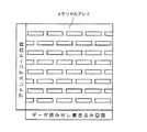
本実施の形態5は、上記実施の形態1,2に係る半導体装置の製造方法を、メモリセルアレイ内に形成される複数のメモリセルトランジスタがそれぞれ有するゲート電極の形成に適用したものである。図24は、本実施の形態5に係るメモリセルアレイの構成を示す上面図である。メモリセルアレイには、アドレスでコード回路及びデータ読み出し書き込み回路にそれぞれ接続された複数のメモリセルトランジスタが、行列状に形成されている。但し図24には、メモリセルトランジスタのゲート電極のみが示されている。
【0064】
まず、シリコン基板上にゲート絶縁膜及びポリシリコン膜をこの順に全面的に形成した後、ポリシリコン膜上にシリコン酸化膜を全面に形成する。次に、第1のフォトマスクを用いた写真製版法及び異方性ドライエッチング法によって、シリコン酸化膜をパターニングする。これにより、同一行に属する複数のメモリセルトランジスタの各ゲート電極の形成予定領域の上方に、図中の破線部分を含む直線状のシリコン酸化膜が、各行ごとに形成される。以上の工程は、上記実施の形態1に係る半導体装置の製造方法における、図6に示した工程までの工程に相当する。
【0065】
次に、第2のフォトマスクを用いた写真製版法及び異方性ドライエッチング法によって、図中の破線部分のシリコン酸化膜を除去する。以上の工程は、上記実施の形態1に係る半導体装置の製造方法における、図12に示した工程までの工程に相当する。
【0066】
次に、残ったシリコン酸化膜をハードマスクに用いてポリシリコン膜をエッチングすることにより、複数のメモリセルトランジスタの各ゲート電極を形成する。かかる工程は、上記実施の形態1に係る半導体装置の製造方法における、図13に示した工程に相当する。
【0067】
このように、本実施の形態5に係る半導体装置の製造方法によれば、上記実施の形態1,2に係る半導体装置の製造方法を、メモリセルアレイ内に形成される複数のメモリセルトランジスタがそれぞれ有するゲート電極の形成に適用する。これにより、行方向に互いに隣接するメモリセルトランジスタの各ゲート電極同士の間隔を、いずれも最小線幅にすることができる。そのため、メモリセルアレイのサイズの縮小化を図ることができる。
【0068】
なお、図24に示したようにゲート電極が行方向に沿って延在するタイプのメモリセルアレイのみならず、図25に示すように、ゲート電極が列方向に沿って延在するタイプのメモリセルアレイを対象として、本実施の形態5に係る発明を適用することも可能である。
【0069】
実施の形態6.
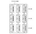
本実施の形態6は、上記実施の形態1,2に係る半導体装置の製造方法を、半導体チップのマクロセル領域内に形成される複数のトランジスタがそれぞれ有するゲート電極の形成に適用したものである。図26は、本実施の形態6に係るマクロセル領域のレイアウト構成を示す上面図である。マクロセル領域には、複数のCMOSトランジスタがマクロセル段(単に「セル段」とも称される)ごとに形成されている。
【0070】
まず、シリコン基板上にゲート絶縁膜及びポリシリコン膜をこの順に全面的に形成した後、ポリシリコン膜上にシリコン酸化膜を全面に形成する。次に、第1のフォトマスクを用いた写真製版法及び異方性ドライエッチング法によって、シリコン酸化膜をパターニングする。これにより、図面の上下方向に沿って並ぶ複数のトランジスタの各ゲート電極の形成予定領域の上方に、図中の破線部分を含む直線状のシリコン酸化膜が、各行ごとに形成される。以上の工程は、上記実施の形態1に係る半導体装置の製造方法における、図6に示した工程までの工程に相当する。
【0071】
次に、第2のフォトマスクを用いた写真製版法及び異方性ドライエッチング法によって、図中の破線部分のシリコン酸化膜を除去する。以上の工程は、上記実施の形態1に係る半導体装置の製造方法における、図12に示した工程までの工程に相当する。
【0072】
次に、残ったシリコン酸化膜をハードマスクに用いてポリシリコン膜をエッチングすることにより、複数のトランジスタの各ゲート電極を形成する。かかる工程は、上記実施の形態1に係る半導体装置の製造方法における、図13に示した工程に相当する。
【0073】
このように、本実施の形態6に係る半導体装置の製造方法によれば、上記実施の形態1,2に係る半導体装置の製造方法を、マクロセル領域内に形成される複数のトランジスタがそれぞれ有するゲート電極の形成に適用する。これにより、異なるセル段に属して隣接するトランジスタのゲート電極同士の間隔を最小線幅にすることができる。そのため、マクロセル領域のサイズの縮小化を図ることができる。
【0074】
【発明の効果】
この発明によれば、ゲート電極のゲート幅よりも幅広の第3の膜を形成した後、第3の膜の端部を除去することによって、第4の膜を形成する。そして、第4の膜をエッチングマスクに用いて第1の膜をエッチングすることによって、ゲート電極を形成する。従って、ゲート電極のゲート幅を正確に設定することができる。
【0075】
また、この発明によれば、第1のゲート電極の形成予定領域の上方から、第2のゲート電極の形成予定領域の上方に繋がって延在する第3の膜を形成した後、第3の膜をパターニングすることにより、第4の膜を形成する。そして、第4の膜をエッチングマスクに用いて第1の膜をエッチングすることにより、第1及び第2のゲート電極を形成する。従って、第1のゲート電極と第2のゲート電極との間隔を、最小線幅にすることができる。その結果、半導体装置の高集積化を図ることができる。
【0076】
また、この発明によれば、最終的に得られるゲート電極のゲート長が短くなるため、半導体装置の動作の高速化を図ることができる。
【0077】
また、この発明によれば、第3の膜を細らせるための等方性エッチングによって第4の膜がエッチングされてゲート幅が変動することを、回避することができる。
【0078】
また、この発明によれば、SRAMメモリセルのセルサイズの縮小化を図ることができる。
【0079】
また、この発明によれば、メモリセルアレイのサイズの縮小化を図ることができる。
【0080】
また、この発明によれば、マクロセル領域のサイズの縮小化を図ることができる。
【図面の簡単な説明】
【図1】 本発明の実施の形態1に係る半導体装置の製造方法を工程順に示す図である。
【図2】 本発明の実施の形態1に係る半導体装置の製造方法を工程順に示す図である。
【図3】 本発明の実施の形態1に係る半導体装置の製造方法を工程順に示す図である。
【図4】 本発明の実施の形態1に係る半導体装置の製造方法を工程順に示す図である。
【図5】 本発明の実施の形態1に係る半導体装置の製造方法を工程順に示す図である。
【図6】 本発明の実施の形態1に係る半導体装置の製造方法を工程順に示す図である。
【図7】 本発明の実施の形態1に係る半導体装置の製造方法を工程順に示す図である。
【図8】 本発明の実施の形態1に係る半導体装置の製造方法を工程順に示す図である。
【図9】 本発明の実施の形態1に係る半導体装置の製造方法を工程順に示す図である。
【図10】 本発明の実施の形態1に係る半導体装置の製造方法を工程順に示す図である。
【図11】 本発明の実施の形態1に係る半導体装置の製造方法を工程順に示す図である。
【図12】 本発明の実施の形態1に係る半導体装置の製造方法を工程順に示す図である。
【図13】 本発明の実施の形態1に係る半導体装置の製造方法を工程順に示す図である。
【図14】 本発明の実施の形態2に係る半導体装置の製造方法を工程順に示す図である。
【図15】 本発明の実施の形態2に係る半導体装置の製造方法を工程順に示す図である。
【図16】 本発明の実施の形態2に係る半導体装置の製造方法を工程順に示す図である。
【図17】 本発明の実施の形態2に係る半導体装置の製造方法を工程順に示す図である。
【図18】 本発明の実施の形態2に係る半導体装置の製造方法を工程順に示す図である。
【図19】 本発明の実施の形態2に係る半導体装置の製造方法を工程順に示す図である。
【図20】 本発明の実施の形態2に係る半導体装置の製造方法を工程順に示す図である。
【図21】本発明の実施の形態2に係る半導体装置の製造方法を工程順に示す図である。
【図22】 本発明の実施の形態3に係るSRAMメモリセルのレイアウト構成を示す上面図である。
【図23】 本発明の実施の形態4に係るSRAMメモリセルのレイアウト構成を示す上面図である。
【図24】 本発明の実施の形態5に係るメモリセルアレイの構成を示す上面図である。
【図25】 本発明の実施の形態5に係る他のメモリセルアレイの構成を示す上面図である。
【図26】 本発明の実施の形態6に係るマクロセル領域のレイアウト構成を示す上面図である。
【図27】 従来の半導体装置の製造方法を工程順に示す図である。
【図28】 従来の半導体装置の製造方法を工程順に示す図である。
【図29】 従来の半導体装置の製造方法を工程順に示す図である。
【図30】 従来の半導体装置の製造方法を工程順に示す図である。
【図31】 従来の半導体装置の製造方法を工程順に示す図である。
【図32】 従来の半導体装置の製造方法を工程順に示す図である。
【図33】 従来の半導体装置の製造方法を工程順に示す図である。
【符号の説明】
1 シリコン基板、4,6,14a,14b,22i〜22k,30a,30b,31i〜31k シリコン酸化膜、5 ポリシリコン膜、7,13a,13b,15 フォトレジスト、10,18 フォトマスク、25i〜25k,35i〜35k ゲート構造。[0001]
BACKGROUND OF THE INVENTION
The present invention relates to a method for manufacturing a semiconductor device, and more particularly to a method for forming a gate electrode of a MOSFET using a photoengraving method and an etching method.
[0002]
[Prior art]
27 to 33 are views showing a conventional method of manufacturing a semiconductor device in the order of steps. 27 (A) to 33 (A) are top views, and FIGS. 27 (B) to 33 (B) are along the line segment X100-X100 shown in FIGS. 27 (A) to 33 (A). It is sectional drawing which shows the cross-sectional structure regarding a position.
[0003]
Referring to FIG. 27, first, a
[0004]
Referring to FIG. 28, next, a
[0005]
Referring to FIG. 29, next, there is a pattern in which openings 111 (indicated by reference numerals 111i to 111k in the drawing) are formed above a region where a gate electrode is to be formed (planned formation region). In other words, the
[0006]
FIG. 30 shows the state of the
[0007]
Referring to FIG. 31, next, the portion of
[0008]
Referring to FIG. 32, next,
[0009]
Referring to FIG. 33, next, using the
[0010]
Thereafter, a silicon oxide film is formed on the entire surface by a CVD method, and then the silicon oxide film is etched back by an anisotropic etching method to form a sidewall on the side surface of the
[0011]
[Problems to be solved by the invention]
Thus, in the conventional method for manufacturing a semiconductor device, the
[0012]
However, when the
[0013]
In order to solve such a problem, a method of predicting the amount of retreat of the
[0014]
The present invention has been made to solve such a problem, and by avoiding the shape of the gate structure from retreating rather than the shape of the opening of the photomask, the gate structure can be formed according to the design dimensions. An object of the present invention is to obtain a method for manufacturing a semiconductor device.
[0015]
[Means for Solving the Problems]
A method of manufacturing a semiconductor device according to a first aspect of the present invention includes: (a) a step of preparing a semiconductor substrate; (b) a step of forming a conductive first film on the semiconductor substrate; ) Forming a second film on the first film; (d) forming a first photoresist on the second film; and (e) a first photo having a first pattern. Using the mask, the step of exposing the first photoresist, (f) the step of developing the first photoresist after being exposed in step (e), and (g) the step of developing by step (f) Then, by patterning the second film using the first photoresist, a third film wider than the gate width of the gate electrode is formed above the region where the gate electrode is to be formed.After that, the first photoresist is removed.And (h) a step executed after step (g), covering the third film and forming a second photoresist on the first film, and (i) a gate width direction of the gate electrode A step of exposing the second photoresist using a second photomask having a second pattern defining the edge of the second photoresist, and (j) the second photoresist after being exposed in step (i) (K) forming a fourth film by patterning the third film using the second photoresist developed in step (j), and (l) A step of etching the first film using the fourth film as an etching mask to form a gate electrode, and (m) executed after the step (g). Further comprising the step of thinning the membrane, Degree (m) is the step (h), The gate electrode is the gate electrode of the memory cell.
[0016]
According to a second aspect of the present invention, there is provided a semiconductor device manufacturing method comprising: (a) a step of preparing a semiconductor substrate; and (b) a step of forming a conductive first film on the semiconductor substrate. (C) forming a second film on the first film; (d) forming a first photoresist on the second film; and (e) a first pattern having a first pattern. A step of exposing the first photoresist using the
[0017]
Moreover, the manufacturing method of the semiconductor device of
[0018]
According to a fourth aspect of the present invention, there is provided a semiconductor device manufacturing method according to the third aspect,The gate electrodes of the first driver transistor and the second access transistor are arranged adjacent to each other with a second predetermined interval in the gate length direction, and the second predetermined interval in the gate length direction. The gate electrodes of the first load transistor and the second load transistor are arranged adjacent to each other, and the first access transistor and the second load transistor are spaced apart from each other in the gate length direction. The gate electrodes of the second driver transistors are arranged adjacent to each other.
[0019]
According to a fifth aspect of the present invention, there is provided a method of manufacturing a semiconductor device according to any one of the first to fourth aspects, wherein the plurality of transistors constituting the SRAM memory cell are respectively provided. The present invention is characterized by being applied to the formation of a gate electrode.
[0020]
According to a sixth aspect of the present invention, there is provided a semiconductor device manufacturing method according to any one of the first to fourth aspects, wherein a plurality of memory cells are formed in a memory cell array. The present invention is characterized in that it is applied to formation of a gate electrode included in each transistor.
[0021]
MaFurther, the present invention claims7(A) a step of preparing a semiconductor substrate, (b) a step of forming a conductive first film on the semiconductor substrate, and (c) on the first film. Forming a second film, (d) patterning the first photoresist on the second film into a first pattern, and (e) second using the first pattern. Form a second pattern by patterning the filmAfter that, the first photoresist is removed.And (f) dividing the second pattern into a plurality of second photoresists that are executed after step (e) and are formed on the first film so as to cover the second pattern. (G) a step of forming a plurality of fourth patterns by patterning the second pattern using the third pattern, and (h) ) Etching the first film using a plurality of fourth patterns as etching masks to form a plurality of gate electrodes; (i) performed after the step (e); Thinning the pattern by isotropic etching, and the step (i) includes the step (f), Each of the plurality of gate electrodes is used for a memory cell, and the first pattern is a pattern extending in the gate width direction of each of the plurality of gate electrodes.
The invention also claims8A method of manufacturing a semiconductor device according to claim7In the method for manufacturing a semiconductor device according to the
The invention also claims9A method of manufacturing a semiconductor device according to claim7The method of manufacturing a semiconductor device according to
The invention also claims10A method of manufacturing a semiconductor device according to claim9Wherein the first driver transistor and the second access transistor are arranged adjacent to each other at a second predetermined interval in the gate length direction. The gate electrodes of the first load transistor and the second load transistor are arranged adjacent to each other at a second predetermined interval in the gate length direction, and the second predetermined interval in the gate length direction. The gate electrodes of the first access transistor and the second driver transistor are arranged adjacent to each other with an interval therebetween.
The invention also claims11A method of manufacturing a semiconductor device according to claim7The method for manufacturing a semiconductor device according to
The invention also claims12A method of manufacturing a semiconductor device according to claim7The method for manufacturing a semiconductor device according to
MaFurther, the present invention claims13A method of manufacturing a semiconductor device according to claim7The method for manufacturing a semiconductor device according to
The invention also claims14The method for manufacturing a semiconductor device according to
The invention also claims15A method of manufacturing a semiconductor device according to claim14The method for manufacturing a semiconductor device according to the
[0022]
DETAILED DESCRIPTION OF THE INVENTION
1 to 13 are views showing the method of manufacturing the semiconductor device according to the first embodiment of the present invention in the order of steps. 1 (A) to 13 (A) are top views, and FIGS. 1 (B) to 13 (B) are along the line segment X1-X1 shown in FIGS. 1 (A) to 13 (A). It is sectional drawing which shows the cross-sectional structure regarding a position.
[0023]
Referring to FIG. 1, first, a
[0024]
Referring to FIG. 2, next, a
[0025]
Referring to FIG. 3, next,
[0026]
The final MOSFET structure is shown in FIG. Comparing FIG. 3A and FIG. 13A, the dimensions of the
[0027]
FIG. 4 shows the state of the
[0028]
Referring to FIG. 5, next, exposed
[0029]
Referring to FIG. 6, next,
[0030]
Referring to FIG. 7, next, a
[0031]
Comparing FIG. 8A and FIG. 13A, the upper ends of the
[0032]
FIG. 9 shows the state of the
[0033]
Referring to FIG. 10, next, exposed portion 20 of
[0034]
Referring to FIG. 11, next, using
[0035]
Referring to FIG. 12, next,
[0036]
Referring to FIG. 13, next, by using the
[0037]
Referring to FIG. 13B, a
[0038]
Thereafter, a silicon oxide film is formed on the entire surface by a CVD method, and then the silicon oxide film is etched back by an anisotropic etching method to form a sidewall on the side surface of the
[0039]
In the above description, after the
[0040]
Thus, according to the manufacturing method of the semiconductor device according to the first embodiment, after forming the
[0041]
Further, after forming the
[0042]
Japanese Patent Laid-Open No. 9-289153 discloses (A) a step of forming a gate oxide film and a gate electrode in this order on a silicon substrate in order to suppress the receding of the tip of the gate electrode due to light interference. (B) a step of forming a first photoresist on the gate electrode, (C) a step of exposing the first photoresist using a first photomask, and (D) a first photoresist. (E) a step of etching the gate electrode using the developed first photoresist as an etching mask, (F) a step of forming a second photoresist, and (G) a second step. A step of exposing the second photoresist using the photomask of (2), (H) a step of developing the second photoresist, and (I) a gate electrode using the developed second photoresist as an etching mask. And etching method for forming a semiconductor device to be executed in this order is described.
[0043]
In this method, the gate electrode is etched in the steps (E) and (I), but the silicon substrate is damaged by each overetching in these two etchings. On the other hand, in the method for manufacturing the semiconductor device according to the first embodiment, the
[0044]
14 to 21 are views showing the method of manufacturing the semiconductor device according to the second embodiment of the present invention in the order of steps. 14 (A) to 21 (A) are top views, and FIGS. 14 (B) to 21 (B) are along the line segment X1-X1 shown in FIGS. 14 (A) to 21 (A). It is sectional drawing which shows the cross-sectional structure regarding a position.
[0045]
First, the structure shown in FIG. 6 is obtained through the same steps as those of the semiconductor device manufacturing method according to the first embodiment. Referring to FIG. 14, next, the entire
[0046]
Referring to FIG. 15, next, a
[0047]
Referring to FIG. 18, next, the exposed portion 20 of the
[0048]
Referring to FIG. 19, next, using
[0049]
Referring to FIG. 20, next,
[0050]
Thereafter, sidewalls are formed on the side surfaces of the
[0051]
As described above, according to the method of manufacturing the semiconductor device according to the second embodiment, the
[0052]
Moreover, the step of thinning the
[0053]
In the third embodiment, the manufacturing method of the semiconductor device according to the first and second embodiments is applied to the formation of gate electrodes respectively included in a plurality of transistors constituting the SRAM memory cell. FIG. 22 is a top view showing the layout configuration of the SRAM memory cell according to the third embodiment. Since such a layout configuration is described in, for example, Japanese Patent Laid-Open No. 10-178110, detailed description thereof is omitted.
[0054]
First, a gate insulating film and a polysilicon film are entirely formed in this order on a silicon substrate, and then a silicon oxide film is entirely formed on the polysilicon film. Next, the silicon oxide film is patterned by photolithography using a first photomask and anisotropic dry etching. As a result, a linear silicon oxide film including a broken line portion in the drawing is formed above the regions where the gate electrodes of the driver transistor N1, the load transistor P1, and the access transistor N4 are to be formed, and the driver transistors N2, A linear silicon oxide film including a broken line portion in the drawing is formed above the regions where the gate electrodes of the load transistor P2 and the access transistor N3 are to be formed. The above steps correspond to the steps up to the step shown in FIG. 6 in the semiconductor device manufacturing method according to the first embodiment.
[0055]
Next, the silicon oxide film in the broken line portion in the figure is removed by photolithography using a second photomask and anisotropic dry etching. The above steps correspond to the steps up to the step shown in FIG. 12 in the semiconductor device manufacturing method according to the first embodiment.
[0056]
Next, the polysilicon film is etched using the remaining silicon oxide film as a hard mask, thereby forming gate electrodes of the various transistors. This process corresponds to the process shown in FIG. 13 in the method for manufacturing the semiconductor device according to the first embodiment.
[0057]
As described above, according to the method for manufacturing a semiconductor device according to the third embodiment, the method for manufacturing the semiconductor device according to the first and second embodiments is performed by using the gate electrodes respectively included in the plurality of transistors constituting the SRAM memory cell. Applies to the formation of Thus, the distance between the gate electrode of the access transistor N4 and the gate electrode of the load transistor P1, the distance between the gate electrode of the access transistor N3 and the gate electrode of the load transistor P2, and the distance between the gate electrodes of the driver transistors adjacent to each other are set. , Both can be set to the minimum line width. Therefore, the cell size can be reduced.
[0058]
In the fourth embodiment, the semiconductor device manufacturing method according to the first and second embodiments is applied to formation of a gate electrode in an SRAM memory cell different from that in FIG. FIG. 23 is a top view showing the layout configuration of the SRAM memory cell according to the fourth embodiment. Since such a layout configuration is described in, for example, Japanese Patent Laid-Open No. 2000-36543, detailed description thereof is omitted.
[0059]
First, a gate insulating film and a polysilicon film are entirely formed in this order on a silicon substrate, and then a silicon oxide film is formed on the entire surface of the polysilicon film. Next, the silicon oxide film is patterned by photolithography using a first photomask and anisotropic dry etching. As a result, a linear silicon oxide film including a broken line portion in the drawing is formed above the formation region of each gate electrode of the driver transistor N1 and the load transistor P1, and each of the driver transistor N2 and the load transistor P2 A linear silicon oxide film including a broken line portion in the figure is formed above the region where the gate electrode is to be formed. The above steps correspond to the steps up to the step shown in FIG. 6 in the semiconductor device manufacturing method according to the first embodiment.
[0060]
Next, the silicon oxide film in the broken line portion in the figure is removed by photolithography using a second photomask and anisotropic dry etching. The above steps correspond to the steps up to the step shown in FIG. 12 in the semiconductor device manufacturing method according to the first embodiment.
[0061]
Next, the polysilicon film is etched using the remaining silicon oxide film as a hard mask, thereby forming gate electrodes of the various transistors. This process corresponds to the process shown in FIG. 13 in the method for manufacturing the semiconductor device according to the first embodiment.
[0062]
Thus, according to the manufacturing method of the semiconductor device according to the fourth embodiment, by applying the manufacturing method of the semiconductor device according to the first and second embodiments to the formation of the gate electrode in the SRAM memory cell, Since the distance between the gate electrodes of the driver transistors adjacent to each other and the distance between the gate electrodes of the load transistors adjacent to each other can be minimized, the cell size can be reduced.
[0063]
In the fifth embodiment, the semiconductor device manufacturing method according to the first and second embodiments is applied to the formation of the gate electrode of each of the plurality of memory cell transistors formed in the memory cell array. FIG. 24 is a top view showing the configuration of the memory cell array according to the fifth embodiment. In the memory cell array, a plurality of memory cell transistors connected to the code circuit and the data read / write circuit by addresses are formed in a matrix. However, only the gate electrode of the memory cell transistor is shown in FIG.
[0064]
First, a gate insulating film and a polysilicon film are entirely formed in this order on a silicon substrate, and then a silicon oxide film is formed on the entire surface of the polysilicon film. Next, the silicon oxide film is patterned by photolithography using a first photomask and anisotropic dry etching. Thereby, a linear silicon oxide film including a broken line portion in the drawing is formed for each row above the region where the gate electrodes of the plurality of memory cell transistors belonging to the same row are to be formed. The above steps correspond to the steps up to the step shown in FIG. 6 in the semiconductor device manufacturing method according to the first embodiment.
[0065]
Next, the silicon oxide film in the broken line portion in the figure is removed by photolithography using a second photomask and anisotropic dry etching. The above steps correspond to the steps up to the step shown in FIG. 12 in the semiconductor device manufacturing method according to the first embodiment.
[0066]
Next, the polysilicon film is etched using the remaining silicon oxide film as a hard mask, thereby forming each gate electrode of the plurality of memory cell transistors. This process corresponds to the process shown in FIG. 13 in the method for manufacturing the semiconductor device according to the first embodiment.
[0067]
Thus, according to the manufacturing method of the semiconductor device according to the fifth embodiment, the manufacturing method of the semiconductor device according to the first and second embodiments is different from that of the plurality of memory cell transistors formed in the memory cell array. The present invention is applied to the formation of a gate electrode. As a result, the interval between the gate electrodes of the memory cell transistors adjacent to each other in the row direction can be set to the minimum line width. Therefore, the size of the memory cell array can be reduced.
[0068]
Note that not only the memory cell array of the type in which the gate electrode extends in the row direction as shown in FIG. 24 but also the memory cell array of the type in which the gate electrode extends in the column direction as shown in FIG. It is also possible to apply the invention according to the fifth embodiment for the above.
[0069]
In the sixth embodiment, the manufacturing method of the semiconductor device according to the first and second embodiments is applied to the formation of gate electrodes respectively included in a plurality of transistors formed in a macro cell region of a semiconductor chip. FIG. 26 is a top view showing the layout configuration of the macro cell area according to the sixth embodiment. In the macro cell region, a plurality of CMOS transistors are formed for each macro cell stage (also simply referred to as “cell stage”).
[0070]
First, a gate insulating film and a polysilicon film are entirely formed in this order on a silicon substrate, and then a silicon oxide film is formed on the entire surface of the polysilicon film. Next, the silicon oxide film is patterned by photolithography using a first photomask and anisotropic dry etching. Thereby, a linear silicon oxide film including a broken line portion in the drawing is formed for each row above the region where the gate electrodes of the plurality of transistors arranged in the vertical direction in the drawing are to be formed. The above steps correspond to the steps up to the step shown in FIG. 6 in the semiconductor device manufacturing method according to the first embodiment.
[0071]
Next, the silicon oxide film in the broken line portion in the figure is removed by photolithography using a second photomask and anisotropic dry etching. The above steps correspond to the steps up to the step shown in FIG. 12 in the semiconductor device manufacturing method according to the first embodiment.
[0072]
Next, the polysilicon film is etched using the remaining silicon oxide film as a hard mask, thereby forming the gate electrodes of the plurality of transistors. This process corresponds to the process shown in FIG. 13 in the method for manufacturing the semiconductor device according to the first embodiment.
[0073]
Thus, according to the method of manufacturing a semiconductor device according to the sixth embodiment, the gates of the plurality of transistors formed in the macro cell region are the same as the method of manufacturing the semiconductor device according to the first and second embodiments. Applies to electrode formation. As a result, the distance between the gate electrodes of adjacent transistors belonging to different cell stages can be reduced to the minimum line width. Therefore, the size of the macro cell area can be reduced.
[0074]
【The invention's effect】
This departureClearlyAccording to this, after the third film having a width wider than the gate width of the gate electrode is formed, the end of the third film is removed to form the fourth film. Then, the gate film is formed by etching the first film using the fourth film as an etching mask. Therefore, the gate width of the gate electrode can be set accurately.
[0075]
This departureClearlyAccording to this, after forming the third film extending from above the region where the first gate electrode is to be formed and extending above the region where the second gate electrode is to be formed, the third film is patterned. Thus, the fourth film is formed. Then, the first and second gate electrodes are formed by etching the first film using the fourth film as an etching mask. Therefore, the distance between the first gate electrode and the second gate electrode can be set to the minimum line width. As a result, high integration of the semiconductor device can be achieved.
[0076]
This departureClearlyAccording to this, since the gate length of the finally obtained gate electrode is shortened, the operation speed of the semiconductor device can be increased.
[0077]
This departureClearlyAccordingly, it is possible to avoid the gate width from being changed due to the etching of the fourth film by the isotropic etching for narrowing the third film.
[0078]
This departureClearlyAccordingly, the cell size of the SRAM memory cell can be reduced.
[0079]
This departureClearlyAccordingly, the size of the memory cell array can be reduced.
[0080]
This departureClearlyAccordingly, the size of the macro cell area can be reduced.
[Brief description of the drawings]
FIG. 1 is a diagram showing a method of manufacturing a semiconductor device according to a first embodiment of the present invention in the order of steps.
FIG. 2 is a diagram showing a method of manufacturing the semiconductor device according to the first embodiment of the present invention in the order of steps.
FIG. 3 is a diagram showing a method of manufacturing the semiconductor device according to the first embodiment of the present invention in the order of steps.
FIG. 4 is a diagram showing the method of manufacturing the semiconductor device according to the first embodiment of the present invention in the order of steps.
FIG. 5 is a diagram showing a method of manufacturing the semiconductor device according to the first embodiment of the present invention in the order of steps.
FIG. 6 is a diagram showing the manufacturing method of the semiconductor device according to the first embodiment of the present invention in the order of steps.
7 is a diagram showing the manufacturing method of the semiconductor device according to the first embodiment of the present invention in the order of steps. FIG.
FIG. 8 is a diagram showing the manufacturing method of the semiconductor device according to the first embodiment of the present invention in the order of steps.
FIG. 9 is a diagram showing the semiconductor device manufacturing method according to the first embodiment of the present invention in the order of steps.
FIG. 10 is a diagram showing the manufacturing method of the semiconductor device according to the first embodiment of the present invention in the order of steps.
FIG. 11 is a diagram showing the semiconductor device manufacturing method according to the first embodiment of the present invention in the order of steps.
FIG. 12 is a diagram showing the semiconductor device manufacturing method according to the first embodiment of the present invention in the order of steps.
FIG. 13 is a diagram showing the semiconductor device manufacturing method according to the first embodiment of the present invention in the order of steps.
FIG. 14 is a diagram showing the method of manufacturing the semiconductor device according to the second embodiment of the present invention in the order of steps.
FIG. 15 is a diagram showing a method of manufacturing the semiconductor device according to the second embodiment of the present invention in the order of steps.
FIG. 16 is a diagram showing the method of manufacturing the semiconductor device according to the second embodiment of the present invention in the order of steps.
FIG. 17 is a diagram showing the method of manufacturing the semiconductor device according to the second embodiment of the present invention in the order of steps.
FIG. 18 is a diagram showing a method of manufacturing the semiconductor device according to the second embodiment of the present invention in the order of steps.
FIG. 19 is a diagram showing the method of manufacturing the semiconductor device according to the second embodiment of the present invention in the order of steps.
FIG. 20 is a diagram showing a method of manufacturing the semiconductor device according to the second embodiment of the present invention in the order of steps.
FIG. 21 is a diagram showing the method of manufacturing the semiconductor device according to the second embodiment of the present invention in the order of steps.
FIG. 22 is a top view showing a layout configuration of an SRAM memory cell according to a third embodiment of the present invention.
FIG. 23 is a top view showing a layout configuration of the SRAM memory cell according to the fourth embodiment of the present invention;
FIG. 24 is a top view showing a configuration of a memory cell array according to the fifth embodiment of the present invention.
FIG. 25 is a top view showing a configuration of another memory cell array according to the fifth embodiment of the present invention.
FIG. 26 is a top view showing a layout configuration of a macro cell area according to a sixth embodiment of the present invention.
FIG. 27 is a diagram showing a conventional method of manufacturing a semiconductor device in the order of steps.
FIG. 28 is a diagram showing a conventional method of manufacturing a semiconductor device in order of steps.
FIG. 29 is a diagram showing a conventional method of manufacturing a semiconductor device in order of steps.
FIG. 30 is a diagram showing a conventional method of manufacturing a semiconductor device in order of steps.
FIG. 31 is a diagram showing a conventional method of manufacturing a semiconductor device in order of steps.
FIG. 32 is a diagram showing a conventional method of manufacturing a semiconductor device in the order of steps.
FIG. 33 is a diagram showing a conventional method of manufacturing a semiconductor device in order of steps.
[Explanation of symbols]
1 silicon substrate, 4, 6, 14a, 14b, 22i to 22k, 30a, 30b, 31i to 31k silicon oxide film, 5 polysilicon film, 7, 13a, 13b, 15 photoresist, 10, 18 photomask, 25i to 25k, 35i-35k gate structure.
Claims (15)
Translated fromJapanese(b)前記半導体基板上に、導電性の第1の膜を形成する工程と、
(c)前記第1の膜上に第2の膜を形成する工程と、
(d)前記第2の膜上に第1のフォトレジストを形成する工程と、
(e)第1のパターンを有する第1のフォトマスクを用いて、前記第1のフォトレジストを露光する工程と、
(f)前記工程(e)によって露光された後の前記第1のフォトレジストを現像する工程と、
(g)前記工程(f)によって現像された後の前記第1のフォトレジストを用いて前記第2の膜をパターニングすることにより、ゲート電極の形成予定領域の上方に、前記ゲート電極のゲート幅よりも幅広の第3の膜を形成し、しかる後に、前記第1のフォトレジストを除去する工程と、
(h)前記工程(g)よりも後に実行され、前記第3の膜を覆って前記第1の膜上に第2のフォトレジストを形成する工程と、
(i)前記ゲート電極のゲート幅方向の端部を規定する第2のパターンを有する第2のフォトマスクを用いて、前記第2のフォトレジストを露光する工程と、
(j)前記工程(i)によって露光された後の前記第2のフォトレジストを現像する工程と、
(k)前記工程(j)によって現像された後の前記第2のフォトレジストを用いて前記第3の膜をパターニングすることにより、第4の膜を形成する工程と、
(l)前記第4の膜をエッチングマスクに用いて前記第1の膜をエッチングすることにより、前記ゲート電極を形成する工程とを備え、
(m)前記工程(g)よりも後に実行され、エッチングによって前記第3の膜を細らせる工程をさらに備え、
前記工程(m)は、前記工程(h)よりも前に実行され、
前記ゲート電極はメモリセルのゲート電極である、半導体装置の製造方法。(A) preparing a semiconductor substrate;
(B) forming a conductive first film on the semiconductor substrate;
(C) forming a second film on the first film;
(D) forming a first photoresist on the second film;
(E) exposing the first photoresist using a first photomask having a first pattern;
(F) developing the first photoresist after being exposed in the step (e);
(G) By patterning the second film using the first photoresist developed in the step (f), the gate width of the gate electrode is formed above the region where the gate electrode is to be formed. Forming a wider third film,and then removing the first photoresist ;
(H) performing a step after the step (g) and forming a second photoresist on the first film so as to cover the third film;
(I) exposing the second photoresist using a second photomask having a second pattern defining an end of the gate electrode in the gate width direction;
(J) developing the second photoresist after being exposed in the step (i);
(K) forming a fourth film by patterning the third film using the second photoresist developed in the step (j);
(L) forming the gate electrode by etching the first film using the fourth film as an etching mask;
(M) further comprising a step executed after the step (g) and thinning the third film by etching;
The step (m) is performed before the step (h ),
A method of manufacturing a semiconductor device, wherein the gate electrode is a gate electrode of a memory cell.
(b)前記半導体基板上に、導電性の第1の膜を形成する工程と、
(c)前記第1の膜上に第2の膜を形成する工程と、
(d)前記第2の膜上に第1のフォトレジストを形成する工程と、
(e)第1のパターンを有する第1のフォトマスクを用いて、前記第1のフォトレジストを露光する工程と、
(f)前記工程(e)によって露光された後の前記第1のフォトレジストを現像する工程と、
(g)前記工程(f)によって現像された後の前記第1のフォトレジストを用いて前記第2の膜をパターニングすることにより、第1のゲート電極の形成予定領域の上方から、ゲート幅方向に沿って前記第1のゲート電極に隣接する第2のゲート電極の形成予定領域の上方に繋がって延在する第3の膜を形成し、しかる後に、前記第1のフォトレジストを除去する工程と、
(h)前記工程(g)よりも後に実行され、前記第3の膜を覆って前記第1の膜上に第2のフォトレジストを形成する工程と、
(i)前記第2のゲート電極側の前記第1のゲート電極の端部、及び前記第1のゲート電極側の前記第2のゲート電極の端部を規定する第2のパターンを有する第2のフォトマスクを用いて、前記第2のフォトレジストを露光する工程と、
(j)前記工程(i)によって露光された後の前記第2のフォトレジストを現像する工程と、
(k)前記工程(j)によって現像された後の前記第2のフォトレジストを用いて前記第3の膜をパターニングすることにより、第4の膜を形成する工程と、
(l)前記第4の膜をエッチングマスクに用いて前記第1の膜をエッチングすることにより、前記第1及び第2のゲート電極を形成する工程とを備え、
(m)前記工程(g)よりも後に実行され、エッチングによって前記第3の膜を細らせる工程をさらに備え、
前記工程(m)は、前記工程(h)よりも前に実行され、
前記第1および第2のゲート電極はメモリセルのゲート電極である、半導体装置の製造方法。(A) preparing a semiconductor substrate;
(B) forming a conductive first film on the semiconductor substrate;
(C) forming a second film on the first film;
(D) forming a first photoresist on the second film;
(E) exposing the first photoresist using a first photomask having a first pattern;
(F) developing the first photoresist after being exposed in the step (e);
(G) By patterning the second film using the first photoresist developed in the step (f), a gate width direction is formed from above the region where the first gate electrode is to be formed. Forming a third film extending along and extending above a region where the second gate electrode adjacent to the first gate electrode is to be formed, and then removing the first photoresist When,
(H) performing a step after the step (g) and forming a second photoresist on the first film so as to cover the third film;
(I) a second pattern having a second pattern defining an end portion of the first gate electrode on the second gate electrode side and an end portion of the second gate electrode on the first gate electrode side; Exposing the second photoresist using a photomask of:
(J) developing the second photoresist after being exposed in the step (i);
(K) forming a fourth film by patterning the third film using the second photoresist developed in the step (j);
(L) forming the first and second gate electrodes by etching the first film using the fourth film as an etching mask;
(M) further comprising a step executed after the step (g) and thinning the third film by etching;
The step (m) is performed before the step (h ),
The method for manufacturing a semiconductor device, wherein the first and second gate electrodes are gate electrodes of a memory cell.
前記メモリセルは第一SRAMメモリセルであり、
前記第一SRAMメモリセルは平面視において、
前記ゲート幅方向に延びる直線状の第一ライン上にゲート電極が延び、NMOSで構成された第一ドライバトランジスタと、
前記第一ライン上にゲート電極が延び、PMOSで構成された第一負荷トランジスタと、
前記第一ライン上にゲート電極が延び、NMOSで構成された第一アクセストランジスタと、
前記第一ラインと平行な直線状の第二ライン上にゲート電極が延び、NMOSで構成された第二アクセストランジスタと、
前記第二ライン上にゲート電極が延び、PMOSで構成された第二負荷トランジスタと、
前記第二ライン上にゲート電極が延び、NMOSで構成された第二ドライバトランジスタとを有するように構成され、
前記第一ラインと前記第二ラインはゲート長方向にて隣り合い、
前記第一ドライバトランジスタと前記第一負荷トランジスタとは互いにゲート電極を共有し、
前記第二負荷トランジスタと前記第二ドライバトランジスタとは互いにゲート電極を共有し、
前記第一SRAMメモリセルと前記ゲート幅方向にて隣り合う第二SRAMメモリセルと前記第二アクセストランジスタとは互いにゲート電極を共有し、
前記第二SRAMメモリセルの反対側に前記第一SRAMメモリセルと前記ゲート幅方向にて隣り合う第三SRAMメモリセルと前記第一アクセストランジスタとは互いにゲート電極を共有し、
前記工程(k)によって、前記ゲート幅方向に第一の所定の間隔を隔てつつ前記第一負荷トランジスタのゲート電極と前記第一アクセストランジスタのゲート電極とが互いに隣り合うように、前記第4の膜がパターニングされ、
前記工程(k)によって、前記ゲート幅方向に前記第一の所定の間隔を隔てつつ前記第二アクセストランジスタのゲート電極と前記第二負荷トランジスタのゲート電極とが互いに隣り合うように、前記第4の膜がパターニングされ、
前記工程(k)によって、前記ゲート幅方向に前記第一の所定の間隔を隔てつつ前記第二SRAMメモリセルのゲート電極と前記第一ドライバトランジスタのゲート電極とが互いに隣り合うように、前記第4の膜がパターニングされ、
前記工程(k)によって、前記ゲート幅方向に前記第一の所定の間隔を隔てつつ前記第三SRAMメモリセルのゲート電極と前記第二ドライバトランジスタのゲート電極とが互いに隣り合うように、前記第4の膜がパターニングされる、請求項1又は2に記載の半導体装置の製造方法。A plurality of the third films are formed by the step (g),
The memory cell is a first SRAM memory cell;
The first SRAM memory cell has a plan view.
A gate electrode extends on a linear first line extending in the gate width direction, and a first driver transistor composed of NMOS,
A gate electrode extending on the first line, and a first load transistor composed of PMOS;
A gate electrode extending on the first line, and a first access transistor composed of NMOS;
A gate electrode extending on a linear second line parallel to the first line, and a second access transistor composed of NMOS;
A gate electrode extending on the second line, and a second load transistor composed of PMOS;
A gate electrode extends on the second line, and is configured to have a second driver transistor composed of NMOS,
The first line and the second line are adjacent in the gate length direction,
The first driver transistor and the first load transistor share a gate electrode with each other,
The second load transistor and the second driver transistor share a gate electrode with each other,
The second SRAM memory cell adjacent to the first SRAM memory cell in the gate width direction and the second access transistor share a gate electrode,
The third SRAM memory cell adjacent to the first SRAM memory cell in the gate width direction on the opposite side of the second SRAM memory cell and the first access transistor share a gate electrode,
In the step (k), the fourth load transistor and the first access transistor are adjacent to each other while being spaced apart from each other by a first predetermined interval in the gate width direction. The film is patterned,
In the step (k), the fourth electrode is arranged such that the gate electrode of the second access transistor and the gate electrode of the second load transistor are adjacent to each other with the first predetermined interval in the gate width direction. Of the film is patterned,
In the step (k), the gate electrode of the second SRAM memory cell and the gate electrode of the first driver transistor are adjacent to each other with the first predetermined interval in the gate width direction. 4 film is patterned,
In the step (k), the gate electrode of the third SRAM memory cell and the gate electrode of the second driver transistor are adjacent to each other with the first predetermined interval in the gate width direction. The method of manufacturing a semiconductor device according to claim 1, wherein the film of 4 is patterned.
前記ゲート長方向に前記第二の所定の間隔を隔てて、前記第一負荷トランジスタ及び前記第二負荷トランジスタのゲート電極が互いに隣り合うように配置され、
前記ゲート長方向に前記第二の所定の間隔を隔てて、前記第一アクセストランジスタ及び前記第二ドライバトランジスタのゲート電極が互いに隣り合うように配置される、請求項3に記載の半導体装置の製造方法。The gate electrodes of the first driver transistor and the second access transistor are arranged adjacent to each other at a second predetermined interval in the gate length direction,
The gate electrodes of the first load transistor and the second load transistor are arranged adjacent to each other with the second predetermined interval in the gate length direction,
4. The semiconductor device according to claim 3, wherein gate electrodes of the first access transistor and the second driver transistor are arranged adjacent to each other with the second predetermined interval in the gate length direction. Method.
(b)前記半導体基板上に、導電性の第1の膜を形成する工程と、 (B) forming a conductive first film on the semiconductor substrate;
(c)前記第1の膜上に第2の膜を形成する工程と、 (C) forming a second film on the first film;
(d)前記第2の膜上の第1のフォトレジストを、第一のパターンにパターニングする工程と、 (D) patterning the first photoresist on the second film into a first pattern;
(e)前記第一のパターンを用いて前記第2の膜をパターニングすることにより、第二のパターンを形成し、しかる後に、前記第1のフォトレジストを除去する工程と、 (E) forming the second pattern by patterning the second film using the first pattern, and then removing the first photoresist;
(f)前記工程(e)よりも後に実行され、前記第1の膜上に前記第二のパターンを覆うように形成される第2のフォトレジストを、前記第二のパターンを複数に分割するような開口部を有する第三のパターンに加工する工程と、 (F) A second photoresist formed after the step (e) and covering the second pattern on the first film is divided into a plurality of the second pattern. Processing into a third pattern having such an opening;
(g)前記第三のパターンを用いて前記第二のパターンをパターニングすることにより、複数の第四のパターンを形成する工程と、 (G) forming a plurality of fourth patterns by patterning the second pattern using the third pattern;
(h)前記複数の第四のパターンをエッチングマスクに用いて前記第1の膜をエッチングすることにより、複数のゲート電極を形成する工程と、 (H) forming the plurality of gate electrodes by etching the first film using the plurality of fourth patterns as etching masks;
(i)前記工程(e)よりも後に実行され、前記第二のパターンを等方性エッチングによってパターンを細らせる工程とを、備え、 (I) performing after the step (e), and thinning the pattern by isotropic etching of the second pattern,
前記工程(i)は、前記工程(f)よりも前に実行され、 The step (i) is performed before the step (f),
前記複数のゲート電極それぞれはメモリセルに用いられ、前記第一のパターンは前記複数のゲート電極それぞれのゲート幅方向に延びるパターンである、半導体装置の製造方法。 Each of the plurality of gate electrodes is used for a memory cell, and the first pattern is a pattern extending in the gate width direction of each of the plurality of gate electrodes.
前記メモリセルは第一SRAMメモリセルであり、 The memory cell is a first SRAM memory cell;
前記第一SRAMメモリセルは平面視において、 The first SRAM memory cell has a plan view.
前記ゲート幅方向に延びる直線状の第一ライン上にゲート電極が延び、NMOSで構成された第一ドライバトランジスタと、 A gate electrode extends on a linear first line extending in the gate width direction, and a first driver transistor composed of NMOS,
前記第一ライン上にゲート電極が延び、PMOSで構成された第一負荷トランジスタと、 A gate electrode extending on the first line, and a first load transistor composed of PMOS;
前記第一ライン上にゲート電極が延び、NMOSで構成された第一アクセストランジスタと、 A gate electrode extending on the first line, and a first access transistor composed of NMOS;
前記第一ラインと平行な直線状の第二ライン上にゲート電極が延び、NMOSで構成された第二アクセストランジスタと、 A gate electrode extending on a linear second line parallel to the first line, and a second access transistor composed of NMOS;
前記第二ライン上にゲート電極が延び、PMOSで構成された第二負荷トランジスタと、 A gate electrode extending on the second line, and a second load transistor composed of PMOS;
前記第二ライン上にゲート電極が延び、NMOSで構成された第二ドライバトランジスタとを有するように構成され、 A gate electrode extends on the second line, and is configured to have a second driver transistor composed of NMOS,
前記第一ラインと前記第二ラインはゲート長方向にて隣り合い、 The first line and the second line are adjacent in the gate length direction,
前記第一ドライバトランジスタと前記第一負荷トランジスタとは互いにゲート電極を共有し、 The first driver transistor and the first load transistor share a gate electrode with each other,
前記第二負荷トランジスタと前記第二ドライバトランジスタとは互いにゲート電極を共有し、 The second load transistor and the second driver transistor share a gate electrode with each other,
前記第一SRAMメモリセルと前記ゲート幅方向にて隣り合う第二SRAMメモリセルと前記第二アクセストランジスタとは互いにゲート電極を共有し、 The second SRAM memory cell adjacent to the first SRAM memory cell in the gate width direction and the second access transistor share a gate electrode,
前記第二SRAMメモリセルの反対側に前記第一SRAMメモリセルと前記ゲート幅方向にて隣り合う第三SRAMメモリセルと前記第一アクセストランジスタとは互いにゲート電極を共有し、 The third SRAM memory cell adjacent to the first SRAM memory cell in the gate width direction on the opposite side of the second SRAM memory cell and the first access transistor share a gate electrode,
前記工程(g)によって、前記ゲート幅方向に第一の所定の間隔を隔てつつ前記第一負荷トランジスタのゲート電極と前記第一アクセストランジスタのゲート電極とが互いに隣り合うように、前記第4の膜がパターニングされ、 In the step (g), the fourth load transistor and the first access transistor are adjacent to each other while being spaced apart from each other by a first predetermined interval in the gate width direction. The film is patterned,
前記工程(g)によって、前記ゲート幅方向に前記第一の所定の間隔を隔てつつ前記第二アクセストランジスタのゲート電極と前記第二負荷トランジスタのゲート電極とが互いに隣り合うように、前記第4の膜がパターニングされ、 The step (g) allows the gate electrode of the second access transistor and the gate electrode of the second load transistor to be adjacent to each other with the first predetermined interval in the gate width direction. Of the film is patterned,
前記工程(g)によって、前記ゲート幅方向に前記第一の所定の間隔を隔てつつ前記第二SRAMメモリセルのゲート電極と前記第一ドライバトランジスタのゲート電極とが互いに隣り合うように、前記第4の膜がパターニングされ、 In the step (g), the gate electrode of the second SRAM memory cell and the gate electrode of the first driver transistor are adjacent to each other with the first predetermined interval in the gate width direction. 4 film is patterned,
前記工程(g)によって、前記ゲート幅方向に前記第一の所定の間隔を隔てつつ前記第三SRAMメモリセルのゲート電極と前記第二ドライバトランジスタのゲート電極とが互いに隣り合うように、前記第4の膜がパターニングされる、請求項7に記載の半導体装置の製造方法。 In the step (g), the gate electrode of the third SRAM memory cell and the gate electrode of the second driver transistor are adjacent to each other with the first predetermined interval in the gate width direction. The method of manufacturing a semiconductor device according to claim 7, wherein the film 4 is patterned.
前記ゲート長方向に前記第二の所定の間隔を隔てて、前記第一負荷トランジスタ及び前記第二負荷トランジスタのゲート電極が互いに隣り合うように配置され、 The gate electrodes of the first load transistor and the second load transistor are arranged adjacent to each other with the second predetermined interval in the gate length direction,
前記ゲート長方向に前記第二の所定の間隔を隔てて、前記第一アクセストランジスタ及び前記第二ドライバトランジスタのゲート電極が互いに隣り合うように配置される、請求項9に記載の半導体装置の製造方法。 10. The semiconductor device manufacture according to claim 9, wherein gate electrodes of the first access transistor and the second driver transistor are arranged adjacent to each other with the second predetermined interval in the gate length direction. Method.
Priority Applications (6)
| Application Number | Priority Date | Filing Date | Title |
|---|---|---|---|
| JP2001177193AJP4776813B2 (en) | 2001-06-12 | 2001-06-12 | Manufacturing method of semiconductor device |
| TW091105185ATW538453B (en) | 2001-06-12 | 2002-03-19 | Method of manufacturing semiconductor device |
| US10/112,770US6670262B2 (en) | 2001-06-12 | 2002-04-02 | Method of manufacturing semiconductor device |
| DE10220395ADE10220395A1 (en) | 2001-06-12 | 2002-05-07 | Method of manufacturing a semiconductor device |
| CNB021200106ACN1201376C (en) | 2001-06-12 | 2002-05-10 | Manufacturing method for semiconductor device |
| KR10-2002-0025716AKR100476404B1 (en) | 2001-06-12 | 2002-05-10 | Method of manufacturing semiconductor device |
Applications Claiming Priority (1)
| Application Number | Priority Date | Filing Date | Title |
|---|---|---|---|
| JP2001177193AJP4776813B2 (en) | 2001-06-12 | 2001-06-12 | Manufacturing method of semiconductor device |
Publications (3)
| Publication Number | Publication Date |
|---|---|
| JP2002367925A JP2002367925A (en) | 2002-12-20 |
| JP2002367925A5 JP2002367925A5 (en) | 2008-07-03 |
| JP4776813B2true JP4776813B2 (en) | 2011-09-21 |
Family
ID=19018074
Family Applications (1)
| Application Number | Title | Priority Date | Filing Date |
|---|---|---|---|
| JP2001177193AExpired - Fee RelatedJP4776813B2 (en) | 2001-06-12 | 2001-06-12 | Manufacturing method of semiconductor device |
Country Status (6)
| Country | Link |
|---|---|
| US (1) | US6670262B2 (en) |
| JP (1) | JP4776813B2 (en) |
| KR (1) | KR100476404B1 (en) |
| CN (1) | CN1201376C (en) |
| DE (1) | DE10220395A1 (en) |
| TW (1) | TW538453B (en) |
Families Citing this family (16)
| Publication number | Priority date | Publication date | Assignee | Title |
|---|---|---|---|---|
| JP4729609B2 (en)* | 2002-07-31 | 2011-07-20 | ルネサスエレクトロニクス株式会社 | Manufacturing method of semiconductor device |
| JP4343571B2 (en) | 2002-07-31 | 2009-10-14 | 株式会社ルネサステクノロジ | Manufacturing method of semiconductor device |
| JP2004103851A (en)* | 2002-09-10 | 2004-04-02 | Renesas Technology Corp | Static semiconductor memory device |
| CN1331212C (en)* | 2004-10-18 | 2007-08-08 | 旺宏电子股份有限公司 | Method for manufacturing integrated circuit |
| US7279386B2 (en)* | 2004-12-03 | 2007-10-09 | Advanced Micro Devices, Inc. | Method for forming a semiconductor arrangement with gate sidewall spacers of specific dimensions |
| US7569073B2 (en)* | 2004-12-29 | 2009-08-04 | Bausch & Lomb Incorporated | Small incision intraocular lens with anti-PCO feature |
| US7473648B2 (en)* | 2006-03-07 | 2009-01-06 | International Business Machines Corporation | Double exposure double resist layer process for forming gate patterns |
| JP2009081420A (en)* | 2007-09-07 | 2009-04-16 | Nec Electronics Corp | Manufacturing method of semiconductor device |
| CN101572218B (en)* | 2008-04-28 | 2011-03-23 | 中芯国际集成电路制造(北京)有限公司 | Methods for forming semiconductor component and gate |
| JP5319247B2 (en)* | 2008-11-14 | 2013-10-16 | 株式会社東芝 | Manufacturing method of semiconductor device |
| US7939384B2 (en)* | 2008-12-19 | 2011-05-10 | Taiwan Semiconductor Manufacturing Company, Ltd. | Eliminating poly uni-direction line-end shortening using second cut |
| JP5661524B2 (en)* | 2011-03-22 | 2015-01-28 | ルネサスエレクトロニクス株式会社 | Manufacturing method of semiconductor integrated circuit device |
| JP6085803B2 (en)* | 2013-02-19 | 2017-03-01 | 富士通セミコンダクター株式会社 | Manufacturing method of semiconductor device |
| KR20170003674A (en)* | 2014-05-27 | 2017-01-09 | 가부시키가이샤 한도오따이 에네루기 켄큐쇼 | Semiconductor device and method for manufacturing the same |
| US12321678B2 (en)* | 2021-05-14 | 2025-06-03 | Mediatek Inc. | Integrated circuit with compact layout arrangement |
| CN117153677B (en)* | 2023-10-27 | 2024-03-01 | 合肥晶合集成电路股份有限公司 | Method for manufacturing semiconductor structure |
Family Cites Families (11)
| Publication number | Priority date | Publication date | Assignee | Title |
|---|---|---|---|---|
| JP2903884B2 (en)* | 1992-07-10 | 1999-06-14 | ヤマハ株式会社 | Semiconductor device manufacturing method |
| US5523258A (en)* | 1994-04-29 | 1996-06-04 | Cypress Semiconductor Corp. | Method for avoiding lithographic rounding effects for semiconductor fabrication |
| JPH09186166A (en)* | 1996-01-08 | 1997-07-15 | Toshiba Corp | Method for manufacturing semiconductor device |
| JPH09289153A (en) | 1996-04-23 | 1997-11-04 | Oki Electric Ind Co Ltd | Manufacture of semiconductor device and mask used therefor |
| JP3523762B2 (en)* | 1996-12-19 | 2004-04-26 | 株式会社東芝 | Semiconductor storage device |
| JP4214428B2 (en) | 1998-07-17 | 2009-01-28 | ソニー株式会社 | Semiconductor memory device |
| KR100333274B1 (en)* | 1998-11-24 | 2002-04-24 | 구본준, 론 위라하디락사 | Liquid Crystal Display and Method Thereof |
| US6426175B2 (en)* | 1999-02-22 | 2002-07-30 | International Business Machines Corporation | Fabrication of a high density long channel DRAM gate with or without a grooved gate |
| JP2001036086A (en)* | 1999-07-15 | 2001-02-09 | Telecommunication Advancement Organization Of Japan | Manufacture of semiconductor device |
| JP3393469B2 (en)* | 1999-07-15 | 2003-04-07 | 日本電気株式会社 | Thin film semiconductor device manufacturing method and thin film semiconductor forming apparatus |
| KR100669862B1 (en)* | 2000-11-13 | 2007-01-17 | 삼성전자주식회사 | Method of forming fine pattern of semiconductor device |
- 2001
- 2001-06-12JPJP2001177193Apatent/JP4776813B2/ennot_activeExpired - Fee Related
- 2002
- 2002-03-19TWTW091105185Apatent/TW538453B/ennot_activeIP Right Cessation
- 2002-04-02USUS10/112,770patent/US6670262B2/ennot_activeExpired - Lifetime
- 2002-05-07DEDE10220395Apatent/DE10220395A1/ennot_activeCeased
- 2002-05-10KRKR10-2002-0025716Apatent/KR100476404B1/ennot_activeExpired - Fee Related
- 2002-05-10CNCNB021200106Apatent/CN1201376C/ennot_activeExpired - Fee Related
Also Published As
| Publication number | Publication date |
|---|---|
| DE10220395A1 (en) | 2003-01-02 |
| US20020187621A1 (en) | 2002-12-12 |
| JP2002367925A (en) | 2002-12-20 |
| KR20020095063A (en) | 2002-12-20 |
| US6670262B2 (en) | 2003-12-30 |
| CN1391258A (en) | 2003-01-15 |
| KR100476404B1 (en) | 2005-03-16 |
| CN1201376C (en) | 2005-05-11 |
| TW538453B (en) | 2003-06-21 |
Similar Documents
| Publication | Publication Date | Title |
|---|---|---|
| JP4776813B2 (en) | Manufacturing method of semiconductor device | |
| US8309469B2 (en) | Method of fabricating semiconductor device | |
| US7906435B2 (en) | Semiconductor device and a manufacturing method thereof | |
| US7352018B2 (en) | Non-volatile memory cells and methods for fabricating non-volatile memory cells | |
| JP2001168205A (en) | Semiconductor device, method of manufacturing the same, and mask used for manufacturing | |
| US20070243707A1 (en) | Hard Mask Layer Stack And A Method Of Patterning | |
| US20070218627A1 (en) | Device and a method and mask for forming a device | |
| TW201539718A (en) | Integrated circuit layout and semiconductor device | |
| JP2003229575A (en) | Integrated semiconductor device and manufacturing method thereof | |
| US20230335545A1 (en) | Method of manufacturing conductors for semiconductor device | |
| JP2003124339A (en) | Semiconductor device and method of manufacturing the same | |
| JP2011258822A (en) | Method of manufacturing semiconductor device | |
| JP2010245173A (en) | Manufacturing method of semiconductor device | |
| JP2952887B2 (en) | Semiconductor device and manufacturing method thereof | |
| US7235442B2 (en) | Method for fabricating conductive line | |
| US8703608B2 (en) | Control of local environment for polysilicon conductors in integrated circuits | |
| US20040029327A1 (en) | Semiconductor device with an improved gate electrode pattern and a method of manufacturing the same | |
| US7851137B2 (en) | Method of manufacturing semiconductor device | |
| JP2008277550A (en) | Manufacturing method of semiconductor device | |
| JP2008108977A (en) | Nonvolatile semiconductor memory, and manufacturing method thereof | |
| CN110707003B (en) | Fabrication method of patterned structure | |
| CN111106001A (en) | Method for forming gate structure of NAND memory, NAND memory and photomask mask | |
| JPH09326475A (en) | Fabrication of nonvolatile memory and exposing mask | |
| JP2011171339A (en) | Method of manufacturing semiconductor device and photomask | |
| JP2011165933A (en) | Method of manufacturing semiconductor device |
Legal Events
| Date | Code | Title | Description |
|---|---|---|---|
| A521 | Request for written amendment filed | Free format text:JAPANESE INTERMEDIATE CODE: A523 Effective date:20080509 | |
| A621 | Written request for application examination | Free format text:JAPANESE INTERMEDIATE CODE: A621 Effective date:20080509 | |
| RD04 | Notification of resignation of power of attorney | Free format text:JAPANESE INTERMEDIATE CODE: A7424 Effective date:20080509 | |
| A711 | Notification of change in applicant | Free format text:JAPANESE INTERMEDIATE CODE: A712 Effective date:20100524 | |
| A977 | Report on retrieval | Free format text:JAPANESE INTERMEDIATE CODE: A971007 Effective date:20101215 | |
| A131 | Notification of reasons for refusal | Free format text:JAPANESE INTERMEDIATE CODE: A131 Effective date:20101221 | |
| A521 | Request for written amendment filed | Free format text:JAPANESE INTERMEDIATE CODE: A523 Effective date:20110204 | |
| A02 | Decision of refusal | Free format text:JAPANESE INTERMEDIATE CODE: A02 Effective date:20110301 | |
| A521 | Request for written amendment filed | Free format text:JAPANESE INTERMEDIATE CODE: A523 Effective date:20110530 | |
| A911 | Transfer to examiner for re-examination before appeal (zenchi) | Free format text:JAPANESE INTERMEDIATE CODE: A911 Effective date:20110606 | |
| TRDD | Decision of grant or rejection written | ||
| A01 | Written decision to grant a patent or to grant a registration (utility model) | Free format text:JAPANESE INTERMEDIATE CODE: A01 Effective date:20110628 | |
| A01 | Written decision to grant a patent or to grant a registration (utility model) | Free format text:JAPANESE INTERMEDIATE CODE: A01 | |
| A61 | First payment of annual fees (during grant procedure) | Free format text:JAPANESE INTERMEDIATE CODE: A61 Effective date:20110629 | |
| R150 | Certificate of patent or registration of utility model | Free format text:JAPANESE INTERMEDIATE CODE: R150 | |
| FPAY | Renewal fee payment (event date is renewal date of database) | Free format text:PAYMENT UNTIL: 20140708 Year of fee payment:3 | |
| S531 | Written request for registration of change of domicile | Free format text:JAPANESE INTERMEDIATE CODE: R313531 | |
| R350 | Written notification of registration of transfer | Free format text:JAPANESE INTERMEDIATE CODE: R350 | |
| LAPS | Cancellation because of no payment of annual fees |