JP4775771B2 - ANTENNA DEVICE AND RADIO COMMUNICATION DEVICE - Google Patents
ANTENNA DEVICE AND RADIO COMMUNICATION DEVICEDownload PDFInfo
- Publication number
- JP4775771B2 JP4775771B2JP2007556454AJP2007556454AJP4775771B2JP 4775771 B2JP4775771 B2JP 4775771B2JP 2007556454 AJP2007556454 AJP 2007556454AJP 2007556454 AJP2007556454 AJP 2007556454AJP 4775771 B2JP4775771 B2JP 4775771B2
- Authority
- JP
- Japan
- Prior art keywords
- antenna device
- electrode
- antenna
- reactance
- circuit
- Prior art date
- Legal status (The legal status is an assumption and is not a legal conclusion. Google has not performed a legal analysis and makes no representation as to the accuracy of the status listed.)
- Expired - Fee Related
Links
- 230000005855radiationEffects0.000claimsdescription124
- 239000003990capacitorSubstances0.000claimsdescription49
- 239000000758substrateSubstances0.000claimsdescription11
- 230000000694effectsEffects0.000description10
- 238000010586diagramMethods0.000description6
- 230000007423decreaseEffects0.000description5
- 230000005540biological transmissionEffects0.000description2
- 239000000126substanceSubstances0.000description2
- 239000004020conductorSubstances0.000description1
- 230000006866deteriorationEffects0.000description1
- 230000005684electric fieldEffects0.000description1
- 230000005669field effectEffects0.000description1
- 238000009434installationMethods0.000description1
- 230000004048modificationEffects0.000description1
- 238000012986modificationMethods0.000description1
- 238000000059patterningMethods0.000description1
Images


Classifications
- H—ELECTRICITY
- H01—ELECTRIC ELEMENTS
- H01Q—ANTENNAS, i.e. RADIO AERIALS
- H01Q1/00—Details of, or arrangements associated with, antennas
- H01Q1/12—Supports; Mounting means
- H01Q1/22—Supports; Mounting means by structural association with other equipment or articles
- H01Q1/24—Supports; Mounting means by structural association with other equipment or articles with receiving set
- H01Q1/241—Supports; Mounting means by structural association with other equipment or articles with receiving set used in mobile communications, e.g. GSM
- H01Q1/242—Supports; Mounting means by structural association with other equipment or articles with receiving set used in mobile communications, e.g. GSM specially adapted for hand-held use
- H01Q1/243—Supports; Mounting means by structural association with other equipment or articles with receiving set used in mobile communications, e.g. GSM specially adapted for hand-held use with built-in antennas
- H—ELECTRICITY
- H01—ELECTRIC ELEMENTS
- H01Q—ANTENNAS, i.e. RADIO AERIALS
- H01Q5/00—Arrangements for simultaneous operation of antennas on two or more different wavebands, e.g. dual-band or multi-band arrangements
- H01Q5/30—Arrangements for providing operation on different wavebands
- H01Q5/307—Individual or coupled radiating elements, each element being fed in an unspecified way
- H01Q5/314—Individual or coupled radiating elements, each element being fed in an unspecified way using frequency dependent circuits or components, e.g. trap circuits or capacitors
- H01Q5/328—Individual or coupled radiating elements, each element being fed in an unspecified way using frequency dependent circuits or components, e.g. trap circuits or capacitors between a radiating element and ground
- H—ELECTRICITY
- H01—ELECTRIC ELEMENTS
- H01Q—ANTENNAS, i.e. RADIO AERIALS
- H01Q5/00—Arrangements for simultaneous operation of antennas on two or more different wavebands, e.g. dual-band or multi-band arrangements
- H01Q5/30—Arrangements for providing operation on different wavebands
- H01Q5/307—Individual or coupled radiating elements, each element being fed in an unspecified way
- H01Q5/342—Individual or coupled radiating elements, each element being fed in an unspecified way for different propagation modes
- H01Q5/357—Individual or coupled radiating elements, each element being fed in an unspecified way for different propagation modes using a single feed point
- H01Q5/364—Creating multiple current paths
- H01Q5/371—Branching current paths
- H—ELECTRICITY
- H01—ELECTRIC ELEMENTS
- H01Q—ANTENNAS, i.e. RADIO AERIALS
- H01Q9/00—Electrically-short antennas having dimensions not more than twice the operating wavelength and consisting of conductive active radiating elements
- H01Q9/04—Resonant antennas
- H01Q9/30—Resonant antennas with feed to end of elongated active element, e.g. unipole
- H01Q9/42—Resonant antennas with feed to end of elongated active element, e.g. unipole with folded element, the folded parts being spaced apart a small fraction of the operating wavelength
Landscapes
- Engineering & Computer Science (AREA)
- Computer Networks & Wireless Communication (AREA)
- Variable-Direction Aerials And Aerial Arrays (AREA)
Description
Translated fromJapaneseこの発明は、小型の携帯電話等に用いられ、多共振で広帯域の送受信が可能なアンテナ装置及び無線通信機に関するものである。 The present invention relates to an antenna device and a wireless communication device that are used in a small mobile phone or the like and are capable of transmitting and receiving a wide band with multiple resonances.
従来、この種のアンテナ装置としては、例えば図19ないし図21に示すようなアンテナ装置がある。
図19は、多共振化を図った従来のアンテナ装置を示す平面図であり、図20は、広帯域化を図った従来のアンテナ装置の平面図であり、図21は、多共振化と広帯域化とを図った従来のアンテナ装置を示す平面図である。Conventionally, as this type of antenna device, for example, there is an antenna device as shown in FIGS.
FIG. 19 is a plan view showing a conventional antenna device with multiple resonances, FIG. 20 is a plan view of a conventional antenna device with wide bandwidths, and FIG. 21 shows multiple resonances and broadbands. It is a top view which shows the conventional antenna device which aimed at.
まず、図19に示すアンテナ装置100は、特許文献1に開示された逆Fアンテナ形状のアンテナ装置であり、接地された複数の追加放射電極111〜113をスイッチ121〜123を介して1つの放射電極101に連結した構造を成す。
すなわち、スイッチ121〜123の切り換えによって、複数の共振周波数を選択することができるようにして、多共振化を図ったアンテナ装置である。First, an
That is, the antenna device is designed to have multiple resonances by selecting a plurality of resonance frequencies by switching the
次に、図20に示すアンテナ装置200は、特許文献2や特許文献3に開示された逆Fアンテナ形状のアンテナ装置であり、追加放射電極210を放射電極201から分岐させ、可変容量素子211を追加放射電極210の先端に接続して、接地した構造を成す。
すなわち、可変容量素子211のインピーダンスを変化させることで、共振周波数をシフトさせることができるようにして、共振周波数の広帯域化を図ったアンテナ装置である。Next, the
In other words, the antenna device is configured to shift the resonance frequency by changing the impedance of the
最後に、図21に示すアンテナ装置300は、特許文献4に開示されたアンテナ装置であり、先端が接地された1つの放射電極301に、接地された複数の追加放射電極311,312をスイッチ321,322を介して連結すると共に、各追加放射電極311(312)の間に、可変容量素子331(332)を介在させた構造を成す。
すなわち、スイッチ321,322の切り換えによって、複数の共振周波数を選択することができるようにして、多共振化を図り、且つ、各可変容量素子331(332)のインピーダンスを変化させることで、各共振周波数をシフトさせることができるようにして、各共振周波数の広帯域化を図ったアンテナ装置である。Finally, the
That is, by switching the
しかし、上記した従来のアンテナ装置では、次のような問題がある。
図19に示したアンテナ装置100では、アンテナ利得の劣化が著しい。
一般に、小型のアンテナ装置では、低い共振周波数を用いる程に、アンテナ利得が下がって、アンテナ効率が劣化する。かかる状況下において、図19に示すアンテナ装置100では、スイッチ123をオン状態にして、最も低い共振周波数を得る構成であるので、スイッチ動作によるロスが発生し、アンテナ利得が下がって、アンテナ効率をさらに劣化させてしまう。
また、このアンテナ装置100では、オン状態のスイッチの内、給電部側に最も近いスイッチを通じて電流が追加放射電極に流れ込む。例えば、追加放射電極111〜113の全部をオン状態にしても、電流が流れ込むのは、給電部400に最も近いスイッチ121だけであり、他のスイッチ122,123には流れ込まない。このため、共振周波数は、スイッチ121〜123の数分しか発生させることができず、共振周波数の種類が少ない。However, the above-described conventional antenna device has the following problems.
In the
In general, in a small antenna device, the lower the resonance frequency, the lower the antenna gain and the lower the antenna efficiency. Under such circumstances, the
In the
図20に示したアンテナ装置200においても、アンテナ効率が劣化する。
すなわち、このアンテナ装置200では、可変容量素子211のみが接地されているので、可変容量素子211の部分の電圧が最小になり、最大の電流が可変容量素子211を流れる。このため、この可変容量素子211の部分での電力消費が大きくなり、アンテナ効率が大きく劣化することとなる。Also in the
That is, in this
図21に示したアンテナ装置300では、アンテナ面積の小型化が困難である。
すなわち、このアンテナ装置300では、最大電圧が、グランド領域402と平行な放射電極301上に発生し、給電部400近傍には発生しない。そして、最小電圧は放射電極301先端に発生する。このため、半波長のアンテナ長でのみ動作し、4分の1波長のアンテナ長では、動作しない。この結果、放射電極301が長くなってしまい、アンテナ面積を小さくすることができない。
さらに、このアンテナ装置300では、給電部側のインピーダンスとアンテナ側のインピーダンスとを全ての周波数においてマッチングさせることが困難である。
つまり、アンテナ装置300のインピーダンスは、放射電極301とグランド領域402との間に生じる浮遊容量を考慮して決められるので、スイッチ321,322の切り換えによって、切り換えの都度、電界最大位置が変化するため、アンテナ設置条件によりインピーダンスの容量成分が大きく変化してしまう。この結果、スイッチ321,322の切り換え状態によって給電部400側とアンテナとのマッチングがとれたりとれなかったりして、全ての共振周波数に対して、正確なマッチングをとることができない。In the
That is, in this
Furthermore, in this
That is, since the impedance of the
この発明は、上述した課題を解決するためになされたもので、多共振化と広帯域化とを図ることができるだけでなく、アンテナ効率の向上と全ての共振周波数における正確なマッチングが可能なアンテナ装置及び無線通信機を提供することを目的とする。 The present invention has been made to solve the above-described problems, and can not only achieve multi-resonance and wide bandwidth, but also can improve antenna efficiency and accurately match at all resonance frequencies. And a wireless communication device.
上記課題を解決するために、請求項1の発明は、その基端部を給電電極の端部に所定間隔で対向させて形成した第1の容量部を介して容量給電され且つ先端部が接地された一の放射電極と、それぞれがこの放射電極からスイッチ素子を介して分岐され且つそれぞれの先端部が接地された複数の追加放射電極とを備えるアンテナ装置であって、一の電極部を放射電極の基端部に所定間隔で対向させることにより、当該一の電極部と基端部とで第2の容量部を形成し、可変容量素子を、第2の容量部に直列又は並列に接続すると共に接地し、各追加放射電極を、一方端がスイッチ素子に接続された電極部と、一方端が接地された電極部とで構成し、これら1対の電極部の他方端間にリアクタンス回路を接続した構成とする。
かかる構成により、全てのスイッチ素子をオフ状態にすることで、複数の追加放射電極が放射電極から電気的に切り離され、アンテナ装置では、放射電極のみが動作し、最も低い周波数で共振する。このような低い周波数では、アンテナ利得が下ろうとするが、図19に示したアンテナ装置と異なり、スイッチ素子がオフ状態であるので、スイッチ動作による電力ロスは生じない。
また、この発明のアンテナ装置は、スイッチ素子のオン,オフ状態によって、「2」の「スイッチ素子数乗」分の種類のアンテナ構成態様を実現することができる。しかし、図19に示したアンテナ装置では、上記したように、このように多くのアンテナ構成態様を実現することができても、共振周波数の数はスイッチ素子の数に限定されてしまう。しかしながら、この発明のアンテナ装置では、リアクタンス回路を各追加放射電極に設けているので、各追加放射電極にインピーダンスが生じ、スイッチ素子がオンになると、電流が当該スイッチ素子を介して分岐された追加放射電極に流れ込む。すなわち、図19に示したアンテナ装置と異なり、電流が、オン状態のスイッチ素子に接続されている全ての追加放射電極に分流することとなる。この結果、アンテナ装置は、「2」の「スイッチ素子数乗」分の数の共振周波数で共振することができる。
そして、可変容量素子の容量を変化させることで、各アンテナ構成態様における共振周波数を連続的に変化させることができる。共振周波数の変化量は、可変容量素子を第2の容量部に並列に接続した場合に最も狭く、第2の容量部に直列に接続した場合、及び可変容量素子を含む並列共振回路を第2の容量部に直列に接続した場合の順で広くなる。
また、接地された可変容量素子が最大電圧部位となる第2の容量部に接続されているので、この可変容量素子に流れ込む電流は、最小となる。この結果、図20に示したアンテナ装置と異なり、可変容量素子で消費される電力が極めて小さくなる。
また、放射電極の先端部が接地されているので、給電時に、電圧が放射電極の先端部で最小になる。そして、給電時に最大電圧部位となる第2の容量部が、放射電極の先端部から最も離れている放射電極の基端部に設けられているので、電圧が当該基端部で最大となる。すなわち、この発明のアンテナ装置は、図21に示したアンテナ装置と異なり、共振周波数における波長の4分の1のアンテナ長で動作する。
さらに、放射電極の基端部に設けられている第2の容量部において最大電圧が生じるので、第2の容量部の容量値は、極めて高く且つ固定的である。したがって、放射電極とグランドとの間に生じる容量がスイッチ素子の切り換えによってほとんど変化せず、図21に示したアンテナ装置と異なり、アンテナ装置のインピーダンスの容量成分は、ほとんど変化しない。In order to solve the above-mentioned problem, the invention of
With this configuration, by turning off all the switch elements, the plurality of additional radiation electrodes are electrically disconnected from the radiation electrode, and in the antenna device, only the radiation electrode operates and resonates at the lowest frequency. At such a low frequency, the antenna gain tends to decrease. However, unlike the antenna device shown in FIG. 19, the switch element is in the OFF state, so that no power loss due to the switch operation occurs.
In addition, the antenna device of the present invention can realize the antenna configuration of the kind corresponding to “2”, which is the “number of switch elements”, depending on the ON / OFF state of the switch elements. However, in the antenna device shown in FIG. 19, as described above, the number of resonance frequencies is limited to the number of switch elements even if such many antenna configuration modes can be realized. However, in the antenna device of the present invention, since the reactance circuit is provided in each additional radiation electrode, an impedance is generated in each additional radiation electrode, and when the switch element is turned on, the current is branched through the switch element. It flows into the radiation electrode. That is, unlike the antenna device shown in FIG. 19, the current is shunted to all the additional radiation electrodes connected to the switch element in the on state. As a result, the antenna apparatus can resonate at a resonance frequency equal to the number of “2” times the “number of switch elements”.
Then, by changing the capacitance of thevariablecapacitance element, it is possible to continuously change the resonance frequency in each antenna configuration form. The amount of change in the resonance frequency is the narrowest when the variable capacitance element is connected in parallel to the second capacitance section, and when the variable capacitance element is connected in series to the second capacitance section, and the parallel resonance circuit including the variable capacitance element is second. It becomes wide in the order when it is connected in series to the capacitor section.
In addition, since the grounded variable capacitance element is connected tothe second capacitance section serving asthe maximum voltage portion,the current flowing into the variable capacitance element is minimized. As a result, unlike the antenna device shown in FIG. 20, the power consumed by the variable capacitance element is extremely small.
Further, since the tip of the radiation electrode is grounded, the voltage is minimized at the tip of the radiation electrode during power feeding. And sincethe 2nd capacity | capacitance part used asthe largest voltage site | part at the time of electric power feeding is provided in the base end part of the radiation electrode furthest away from the front-end | tip part of a radiation electrode, a voltage becomes the maximum in the said base end part. That is, unlike the antenna device shown in FIG. 21, the antenna device of the present invention operates with an antenna length that is a quarter of the wavelength at the resonance frequency.
Furthermore, since the maximum voltage is generated inthe second capacitor portion provided at the base end portion of the radiation electrode, the capacitance value of the second capacitor portion is extremely high and fixed. Therefore, the capacitance generated between the radiation electrode and the ground hardly changes due to switching of the switch element, and unlike the antenna device shown in FIG. 21, the capacitance component of the impedance of the antenna device hardly changes.
請求項2の発明は、請求項1に記載のアンテナ装置において、複数の追加放射電極のそれぞれに設けたリアクタンス回路の内、少なくとも1つのリアクタンス回路は、キャパシタを含む構成とした。
かかる構成により、キャパシタを含むリアクタンス回路を有した追加放射電極のスイッチ素子がオン状態になると、当該キャパシタの近くで動作している追加放射電極が有するインダクタと当該キャパシタとが並列共振回路を構成し、この並列共振回路がバンドストップフィルタとして機能する状態が生じる。このため、1種類のアンテナ構成態様において、並列共振回路がバンドストップフィルタとして機能している場合における共振周波数と、バンドストップフィルタとして機能していない場合における共振周波数との2種類の共振周波数を得ることができる。According to a second aspect of the present invention, in the antenna device according to the first aspect, at least one of the reactance circuits provided in each of the plurality of additional radiation electrodes includes a capacitor.
With this configuration, when the switch element of the additional radiation electrode having the reactance circuit including the capacitor is turned on, the inductor included in the additional radiation electrode operating near the capacitor and the capacitor constitute a parallel resonance circuit. The parallel resonant circuit functions as a band stop filter. Therefore, in one type of antenna configuration, two types of resonance frequencies are obtained: a resonance frequency when the parallel resonance circuit functions as a band stop filter and a resonance frequency when the parallel resonance circuit does not function as a band stop filter. be able to.
請求項3の発明は、請求項1又は請求項2に記載のアンテナ装置において、複数の追加放射電極のそれぞれに設けたリアクタンス回路の内、少なくとも1つのリアクタンス回路は、可変容量素子を含む構成とした。
かかる構成により、追加放射電極に設けられたリアクタンス回路の可変容量素子の容量を変化させることで、この追加放射電極で構成されるアンテナ構成態様における共振周波数を連続的に変化させることができる。According to a third aspect of the present invention, in the antenna device according to the first or second aspect, at least one of the reactance circuits provided in each of the plurality of additional radiation electrodes includes a variable capacitance element. did.
With this configuration, by changing the capacitance of the variable capacitance element of the reactance circuit provided in the additional radiation electrode, it is possible to continuously change the resonance frequency in the antenna configuration mode configured by the additional radiation electrode.
請求項4の発明は、請求項1ないし請求項3のいずれかに記載のアンテナ装置において、複数の追加放射電極のそれぞれに設けたリアクタンス回路の内、少なくとも1つのリアクタンス回路は、直列共振回路又は並列共振回路である構成とした。
かかる構成により、直列共振回路又は並列共振回路のリアクタンス値を設定することで、所望の共振周波数を得ることができる。特に並列共振回路にすることで、バンドストップフィルタとして用いることができ、この結果、1つのアンテナ構成態様で2種類の共振周波数を得ることができる。According to a fourth aspect of the present invention, in the antenna device according to any one of the first to third aspects, at least one of the reactance circuits provided in each of the plurality of additional radiation electrodes is a series resonant circuit or The configuration is a parallel resonant circuit.
With this configuration, a desired resonance frequency can be obtained by setting the reactance value of the series resonance circuit or the parallel resonance circuit. In particular, by using a parallel resonant circuit, it can be used as a band stop filter. As a result, two types of resonant frequencies can be obtained with one antenna configuration.
請求項5の発明は、請求項1ないし請求項4のいずれかに記載のアンテナ装置において、可変容量素子にインダクタを並列に接続して並列共振回路を形成した構成とする。According to a fifth aspect of the present invention, in the antenna device according to any one of the first to fourth aspects, aninductor is connected in parallel to the variable capacitance element to form a parallel resonance circuit .
請求項6の発明は、請求項1ないし請求項5のいずれかに記載のアンテナ装置において、放射電極と複数の追加放射電極とを、誘電体基体上にパターン形成した構成とする。
かかる構成により、誘電体基体によって、容量部の容量値、放射電極と追加放射電極との間の容量値及び追加放射電極間の容量値等を高めることができる。According to a sixth aspect of the present invention, in the antenna device according to any one of the first to fifth aspects, the radiation electrode and a plurality of additional radiation electrodes are patterned on a dielectric substrate.
With this configuration, it is possible to increase the capacitance value of the capacitance portion, the capacitance value between the radiation electrode and the additional radiation electrode, the capacitance value between the additional radiation electrodes, and the like by the dielectric substrate.
請求項7の発明に係る無線通信機は、請求項1ないし請求項6のいずれかに記載のアンテナ装置を具備する構成とした。 According to a seventh aspect of the present invention, there is provided a wireless communication device including the antenna device according to any one of the first to sixth aspects.
以上詳しく説明したように、この発明のアンテナ装置によれば、スイッチ素子がオフ状態で、低周波の共振を行い、スイッチ動作による電力ロスが生じないので、アンテナ利得を上げて、アンテナ効率を向上させることができる。
また、「2」の「スイッチ素子数乗」という多数種類の共振周波数を得ることができるので、デジタルテレビ等のように多チャンネルの放送の受信にも十分対応することができる。そして、可変容量素子の容量を変化させることで、各アンテナ構成態様における共振周波数を連続的に変化させることができるので、共振周波数の広帯域化を図ることができる。
また、接地された可変容量素子で消費される電力が極めて小さいので、この点からもアンテナ効率を向上させることができる。
また、この発明のアンテナ装置は、4分の1波長で動作するので、放射電極等の電極の長さをその分短くすることができ、この結果、アンテナ面積の狭小化を図ることができる。
さらに、スイッチ素子の切り換えによって、アンテナ装置の電流分布が、ほとんど変化しないので、全ての共振周波数に対して、給電側と正確なマッチングを行うことができる。
また、共振周波数の広帯域化を図ることができるだけでなく、可変容量素子と第2の容量部との並列接続、可変容量素子と第2の容量部との直列接続のいずれかの構成を選択することで、共振周波数の変化量を所望量に調整することができる。As described above in detail, according to the antenna device of the present invention, the switching element performs resonance at a low frequency with the switch element turned off, and no power loss due to switching operation occurs, so the antenna gain is increased and the antenna efficiency is improved. Can be made.
In addition, since it is possible to obtain a large number of resonance frequencies of “2”, which is “the number of switch elements”, it is possible to sufficiently handle reception of multi-channel broadcasts such as digital television. Then, by changing the capacitance of the variable capacitance element, the resonance frequency in each antenna configuration mode can be continuously changed, so that the resonance frequency can be widened.
In addition, since the power consumed by the grounded variable capacitor is extremely small, the antenna efficiency can be improved from this point.
Further, since the antenna device of the present invention operates at a quarter wavelength, the length of the electrode such as the radiation electrode can be shortened accordingly, and as a result, the antenna area can be reduced.
Furthermore, since the current distribution of the antenna device hardly changes by switching the switch element, accurate matching with the power feeding side can be performed for all resonance frequencies.
Further, not only can the resonance frequency be broadened, but either a parallel connection of the variable capacitance element and the second capacitance portion or a series connection of the variable capacitance element and the second capacitance portion is selected. Thus, the amount of change in the resonance frequency can be adjusted to a desired amount.
また、請求項2の発明に係るアンテナ装置によれば、1種類のアンテナ構成態様において、2種類の共振周波数を得ることができるので、さらなる多共振化を図ることができる。
また、請求項3の発明に係るアンテナ装置によれば、リアクタンス回路の可変容量素子の容量を変化させることで、共振周波数を連続的に変化させることができるので、その分、帯域幅を広げることができる。
さらに、請求項4の発明に係るアンテナ装置によれば、周波数の帯域幅を広げることができると共に、さらなる多共振化を図ることができる。
また、請求項5の発明に係るアンテナ装置によれば、並列共振回路によって、共振周波数の変化量を所望量に調整することができる。According to the antenna device of the second aspect of the present invention, since two types of resonance frequencies can be obtained in one type of antenna configuration, further multiple resonances can be achieved.
According to the antenna device of the third aspect of the invention, since the resonance frequency can be continuously changed by changing the capacitance of the variable capacitance element of the reactance circuit, the bandwidth is increased accordingly. Can do.
Furthermore, according to the antenna device of the fourth aspect of the invention, the frequency bandwidth can be widened and further multiple resonances can be achieved.
According to the antenna device of the fifth aspect of the present invention, the amount of change in the resonance frequency can be adjusted to a desired amount by the parallel resonance circuit.
請求項6の発明に係るアンテナ装置によれば、容量部の容量値や放射電極と追加放射電極との間の容量値、及び追加放射電極間の容量値等を高めることができるので、短い電極で長いアンテナ長を得ることができ、この結果、アンテナ装置の小型化を図ることができる。 According to the antenna device of the sixth aspect of the invention, it is possible to increase the capacitance value of the capacitance portion, the capacitance value between the radiation electrode and the additional radiation electrode, the capacitance value between the additional radiation electrodes, and the like. Thus, a long antenna length can be obtained, and as a result, the antenna device can be miniaturized.
また、請求項7の発明に係る無線通信機によれば、多共振で広帯域の送受信が可能で、しかも、高アンテナ効率で動作特性の良い通信が可能となる。
以上詳しく説明したように、請求項1ないし請求項9の発明に係るランド構造によれば、Further, according to the wireless communication device of the seventh aspect of the invention, it is possible to transmit and receive a wide band with multiple resonances and to perform communication with high antenna efficiency and good operating characteristics.
As explained in detail above, according to the land structure of the invention of
以下、この発明の最良の形態について図面を参照して説明する。 The best mode of the present invention will be described below with reference to the drawings.
(実施例1)
図1は、この発明の第1実施例に係るアンテナ装置を示す平面図である。
この実施例のアンテナ装置1は、携帯電話やPCカード等の無線通信機に設けられている。
図1に示すように、アンテナ装置1は、無線通信機の回路基板の非グランド領域401に形成されており、グランド領域402上に搭載されている給電部としての送受信部400との間で高周波信号のやり取りを行う。
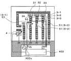
このアンテナ装置1は、1つの放射電極2とこの放射電極2から分岐された複数の追加放射電極3−1〜3−3とを有している。Example 1
FIG. 1 is a plan view showing an antenna apparatus according to a first embodiment of the present invention.
The
As shown in FIG. 1, the
This
放射電極2は、コ字状に折れ曲がった導体パターンであり、その先端部2aがグランド領域402に接地されている。
そして、高周波の電力が給電部400からこの放射電極2に容量給電される構造になっている。具体的には、水平な電極部21が放射電極2の基端部2bに設けられ、この電極部21が、給電部400に接続された給電電極20と対向して第1の容量部である容量部C1を形成している。The
In addition, high-frequency power is capacitively supplied from the
また、かかる放射電極2の基端部2bには、第2の容量部である容量部C2が形成されている。具体的には、電極部22を電極部21に対向させて配置することで、容量部C2を形成し、可変容量素子4をこの容量部C2の後段に直列に接続して接地した。
ここで、容量部C2は、給電部400から放射電極2への給電時に、最大電圧部位となるように設定されており、その容量値は極めて大きい。
また、可変容量素子4としては、バリキャップ、MEMS(Micro Electro Mechanical Systems)等を用いることができる。なお、固定コンデンサ内に強誘電体を充填し、この強誘電体に電圧を与えることで、このコンデンサの容量を変化させることができるので、かかるコンデンサを可変容量素子4として適用することもできる。そして、かかる可変容量素子4の容量制御を、制御IC403からの直流制御電圧によって行う。In addition,a capacitor portion C2 that is a second capacitor portion is formed at the
Here, the capacity portion C2 is set to be the maximum voltage portion when power is supplied from the
Moreover, as the
一方、追加放射電極3−1〜3−3は、スイッチ素子31〜33を介して放射電極2に接続されており、スイッチ素子31〜33がオン状態の時に、これらの追加放射電極3−1〜3−3が放射電極2に電気的に接続され、スイッチ素子31〜33がオフ状態の時に、放射電極2から電気的に切り離されるようになっている。
このようなスイッチ素子31〜33として、ショットキーダイオード、PINダイオード、MEMS、FET(Field Effect Transistor )やSPDT(Single Pole Double Throw)等を用いることができ、かかるスイッチ素子31〜33の切り換え制御を、制御IC403からの直流制御電圧によって行う。On the other hand, the additional radiation electrodes 3-1 to 3-3 are connected to the
As
また、各追加放射電極3−1(3−2,3−3)には、リアクタンス回路5−1(5−2,5−3)を介設している。つまり、各追加放射電極3−1(3−2,3−3)を、放射電極2側の電極部3Aとグランド領域402側の電極部3Bとで構成し、リアクタンス回路5−1(5−2,5−3)を電極部3Aと電極部3Bとの間に接続している。そして、各追加放射電極3−1(3−2,3−3)の電極部3Bの先端部をグランド領域402に接地した。
リアクタンス回路5−1(5−2,5−3)として、後述するように、キャパシタ、インダクタ、直列共振回路、並列共振回路等を用いることができる。また、リアクタンス回路5−1(5−2,5−3)にバリキャップ等の可変容量素子を含めた場合には、破線で示すように、制御IC403からの直流制御電圧で当該可変容量素子の容量を変化させることで、リアクタンス回路5−1(5−2,5−3)のリアクタンス値を変化させることができる。Each additional radiation electrode 3-1 (3-2, 3-3) is provided with a reactance circuit 5-1 (5-2, 5-3). That is, each additional radiation electrode 3-1 (3-2, 3-3) is composed of the
As the reactance circuit 5-1 (5-2, 5-3), as will be described later, a capacitor, an inductor, a series resonance circuit, a parallel resonance circuit, or the like can be used. Further, when a variable capacitance element such as a varicap is included in the reactance circuit 5-1 (5-2, 5-3), as indicated by a broken line, a DC control voltage from the
次に、この実施例のアンテナ装置が示す作用及び効果について説明する。
図2は、この実施例のアンテナ装置1の概略図である。
図2に示す給電部400から給電電極20に給電されると、電力が容量部C1を介して放射電極2に給電され、共振状態時において、電圧が放射電極2の接地された先端部2aで最小Vminになり、基端部2bの容量部C2の部位で最大Vmaxとなる。すなわち、電圧は、容量部C2で最大Vmaxになり、放射電極2の先端部2aに向かうに従って下降し、接地された先端部2aで最小Vminに成る。したがって、このアンテナ装置1は、図21に示した従来のアンテナ装置と異なり、共振周波数における波長の4分の1のアンテナ長で動作する。この結果、放射電極2等の長さを図21に示した従来のアンテナ装置に比べて短くすることができ、アンテナ面積の狭小化を図ることができる。Next, operations and effects of the antenna device of this embodiment will be described.
FIG. 2 is a schematic diagram of the
When electric power is supplied from the electric
図3は、追加放射電極への電流の流れ込み状態を示す概略図である。
図3の(a)は、図19に示したアンテナ装置を模したものであり、追加放射電極3−1(3−2,3−3)にリアクタンス回路5−1(5−2,5−3)を有していない。このようなアンテナ装置では、放射電極2には、Z1〜Z3等のインピーダンスが生じるが、追加放射電極3−1(3−2,3−3)にはインピーダンスが生じない。このため、スイッチ素子31がオン状態になると、スイッチ素子32,33がオン状態であろうがなかろうが、電流Iはインピーダンスがゼロの追加放射電極3−1に全て流れてしまう。この結果、図3の(a)の構成では、8種類のアンテナ構成態様を得ることができるが、共振周波数はスイッチ素子31〜33の数「3」だけしか得ることができない。
これに対して、図3の(b)に示すこの実施例のアンテナ装置1では、追加放射電極3−1(3−2,3−3)にリアクタンス回路5−1を有しているので、放射電極2のインピーダンスZ1〜Z3の他に、追加放射電極3−1〜3−3にも、リアクタンス回路5−1〜5−3)によるインピーダンスZ5〜Z7が生じる。このため、スイッチ素子31がオン状態である場合には、スイッチ素子32,33がオン状態かオフ状態かによって、電流がスイッチ素子32,33に流れ込んだり、流れ込まなかったりする。つまり、オン状態のスイッチ素子31〜33のインピーダンスに対応した電流I1〜I3が当該オン状態のスイッチ素子31〜33を介して追加放射電極3−1〜3−3に分流すると共に、電流I4が放射電極2の先端部側に分流する。この結果、図3の(b)の構成では、8つのアンテナ構成態様と同数の共振周波数を得ることができる。
このように、この実施例のアンテナ装置1では、図19に示したアンテナ装置に比べてより多くの共振周波数を得ることができる。FIG. 3 is a schematic view showing a state of current flowing into the additional radiation electrode.
FIG. 3A illustrates the antenna device shown in FIG. 19, and the reactance circuit 5-1 (5-2, 5--3) is added to the additional radiation electrode 3-1 (3-2, 3-3). Does not have 3). In such an antenna device, impedances such as Z1 to Z3 are generated in the
On the other hand, in the
Thus, in the
図4は、アンテナ構成態様を示す概略図である。
図2において、給電部400から給電すると、スイッチ素子31〜33のオン,オフ状態に応じて各アンテナ構成態様で共振する。アンテナ構成態様は、スイッチ素子31〜33のオン,オフ状態によって実現され、「2」の「スイッチ素子数乗」分の種類の態様がある。この実施例では、スイッチ素子が3つであるので、「2」の「3乗」、即ち、図4の(a)〜(h)に示すような8種類のアンテナ構成態様を得ることができる。FIG. 4 is a schematic diagram showing an antenna configuration mode.
In FIG. 2, when power is supplied from the
図5は、図4における8種類のアンテナ構成態様における共振周波数のリターンロス曲線図である。
図4に示す態様のアンテナ構成において、図4の(a)に示すように、全てのスイッチ素子31〜33をオン状態にした場合の共振周波数f8が最も高く、図4の(b)〜(g)に示すように、スイッチ素子31〜33のいずれかをオフ状態にしていくことで、共振周波数f7〜f2の順で高さが下がっていき、スイッチ素子31〜33の全てをオフ状態にした場合の共振周波数f1が最も低くなる。
これにより、図5のリターンロス曲線S1〜S8に示すように、アンテナ装置1は、異なる8種類の共振周波数f1〜f8を用いて送受信することが可能となる。
ところで、最も低い共振周波数f1で送受信すると、図19に示したアンテナ装置のように、アンテナ利得が問題となるが、この実施例では、図4の(h)に示すように、スイッチ素子31〜33の全てをオフ状態にして共振周波数f1を得るので、図19に示したアンテナ装置と異なり、スイッチ動作によるアンテナ利得の劣化は生じない。FIG. 5 is a return loss curve diagram of resonance frequencies in the eight antenna configuration modes in FIG.
In the antenna configuration shown in FIG. 4, as shown in FIG. 4A, the resonance frequency f <b> 8 is highest when all the
Thereby, as shown in return loss curves S1 to S8 in FIG. 5, the
By the way, when transmitting and receiving at the lowest resonance frequency f1, the antenna gain becomes a problem as in the antenna device shown in FIG. 19, but in this embodiment, as shown in FIG. Since all of 33 are turned off and the resonance frequency f1 is obtained, unlike the antenna device shown in FIG. 19, the antenna gain is not deteriorated by the switching operation.
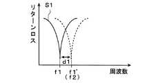
図6は、共振周波数の変化に伴うリターンロス曲線図である。
ここで、図1の構成において、制御IC403から直流制御電圧を可変容量素子4に入力することで、可変容量素子4の容量値を変えることができる。例えば、図6に示すように、上記共振周波数f1の共振状態において、可変容量素子4の容量値を連続的に変化させることで、共振周波数f1を共振周波数f1′まで変化量d1だけシフトさせることができる。したがって、共振周波数f1を隣の共振周波数f2まで移動させることで、共振周波数f1〜f2の範囲で送受信が可能となる。つまり、図5に示す8つの共振周波数f1〜f8は、離散的であるが、各アンテナ構成態様において、可変容量素子4の容量を変化させることで、共振周波数f1〜f8の隙間を埋めて、周波数の広帯域化を図ることができる。FIG. 6 is a return loss curve diagram according to the change of the resonance frequency.
Here, in the configuration of FIG. 1, the capacitance value of the
ところで、上記のように機能する可変容量素子4が接地されていることから、可変容量素子4に大きな電流が流れ、無駄に電力が消費されるおそれがある。しかしながら、図1及び図2に示したように、この実施例では、可変容量素子4が最大電圧部位である容量部C2の直近に接続されているので、可変容量素子4の部位も電圧が大きくなり、可変容量素子4に流れ込む電流が、非常に少なくなる。この結果、可変容量素子4で消費される電力は極めて小さくなる。 By the way, since the
また、この実施例のアンテナ装置1では、容量部C2を、給電部400から放射電極2への給電時に、最大電圧部位となるように設定し、その容量値を極めて大きく設定している。したがって、スイッチ素子31〜33の切り換えによる浮遊容量の変化が生じた場合でも、アンテナ装置1全体のインピーダンスの容量成分の大部分が容量部C2に依存するため、電流分布が変化しない。この結果、全ての共振周波数に対して、給電部400側と正確なマッチングが行われる。 Further, in the
(実施例2)
次に、この発明の第2実施例について説明する。
図7は、この発明の第2実施例に係るアンテナ装置を示す平面図である。
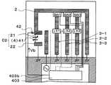
この実施例のアンテナ装置は、第1実施例のスイッチ素子31〜33とリアクタンス回路5−1〜5−3と可変容量素子4とに対して具体的な素子を適用したものである。(Example 2)
Next explained is the second embodiment of the invention.
FIG. 7 is a plan view showing an antenna apparatus according to the second embodiment of the present invention.
In the antenna apparatus of this embodiment, specific elements are applied to the
すなわち、図7に示すように、スイッチ素子31〜33として、ショットキーダイオード31〜33を適用し、各ショットキーダイオード31(32,33)のアノード側を放射電極2に接続すると共にカソード側を追加放射電極3−1(3−2,3−3)の電極部3Aに接続した。
また、可変容量素子4としては、バリキャップ41を適用し、バリキャップ41のカソード側を電極部22に接続すると共にアノード側を接地した。
さらに、リアクタンス回路5−1〜5−3として、インダクタ51〜51を適用し、各インダクタ51の両端を追加放射電極3−1(3−2,3−3)の電極部3A,3Bに接続した。That is, as shown in FIG. 7, Schottky diodes 31-33 are applied as the switch elements 31-33, and the anode side of each Schottky diode 31 (32, 33) is connected to the
Further, as the
Furthermore, as the reactance circuits 5-1 to 5-3,
ショットキーダイオード31(32,33)のオン,オフ動作は、制御IC403から直流制御電圧Vcによって制御する。具体的には、ライン403aを追加放射電極3−1(3−2,3−3)の電極部3Bに抵抗35(例えば100kΩ)を介して接続し、直流制御電圧Vcをこのライン403aを通じてショットキーダイオード31(32,33)のカソード側に印加するようにしている。これにより、例えば、2(V)の直流制御電圧Vcを印加することで、ショットキーダイオード31(32,33)をオン状態にすることができ、0(V)の直流制御電圧Vcを印加することで、オフ状態にすることができる。そして、キャパシタ34(例えば1000(pF))を、各追加放射電極3−1(3−2,3−3)の電極部3Bに介設して、直流制御電圧Vcのグランド領域402側への流出を防止している。 The on / off operation of the Schottky diode 31 (32, 33) is controlled by the
バリキャップ41の容量調整は、制御IC403から直流制御電圧Vbによって制御される。具体的には、ライン403bを容量部C2の電極部22に抵抗42(例えば100kΩ)を介して接続し、直流制御電圧Vbをこのライン403bを通じてバリキャップ41のカソード側に印加するようになっている。これにより、例えば、0(V)〜3(V)の範囲の直流制御電圧Vbを印加することで、バリキャップ41の容量を連続的に変化させることができる。なお、ライン403bに設けられた抵抗42は、各共振時の高周波がライン403bを通じて制御IC403側に流出することを防止するための素子である。 The capacity adjustment of the
ここで、インダクタ51として、チップ部品だけでなく、電極部3A,3B間にパターン形成したメアンダライン等も用いることができる。
追加放射電極3−1〜3−3の全てのインダクタ51のインダクタンス値を等しく設定し、又は異ならしめるなどして、ショットキーダイオード31〜33の切り換えの際に生じる各アンテナ構成態様の共振周波数を任意に変更することができる。
なお、ライン403aに設けられた抵抗35は、各共振時の高周波がライン403aを通じて制御IC403側に流出することを防止するための素子である。Here, as the
By setting the inductance values of all the
The
かかる構成により、制御IC403からの0(V)又は2(V)の直流制御電圧Vcを追加放射電極3−1〜3−3に入力して、ショットキーダイオード31〜33を切り換えることにより、インダクタ51のインダクタンス値に対応した8種類の共振周波数f1〜f8(図5参照)を得ることができる。
そして、制御IC403からの0(V)〜3(V)の直流制御電圧Vbを電極部22に入力して、バリキャップ41の容量値を連続的に変化させることにより、各アンテナ構成態様における共振周波数をシフトさせることができる(図6参照)。
その他の構成、作用及び効果は、上記第1実施例と同様であるので、その記載は省略する。With this configuration, a DC control voltage Vc of 0 (V) or 2 (V) from the
Then, the DC control voltage Vb of 0 (V) to 3 (V) from the
Since other configurations, operations, and effects are the same as those in the first embodiment, description thereof is omitted.
(実施例3)
次に、この発明の第3実施例について説明する。
図8は、この発明の第3実施例に係るアンテナ装置を示す平面図であり、図9は、2共振状態を説明するための概略図であり、図10は、2つの共振周波数に伴うリターンロス曲線図である。
この実施例のアンテナ装置は、追加放射電極3−1〜3−3のリアクタンス回路5−1〜5−3の内、少なくとも1つのリアクタンス回路を、キャパシタで形成した点が、上記第1及び第2実施例と異なる。
具体的には、図8に示すように、リアクタンス回路5−1をキャパシタ52で形成し、リアクタンス回路5−2,5−3をインダクタ51でそれぞれ形成した。(Example 3)
Next explained is the third embodiment of the invention.
FIG. 8 is a plan view showing an antenna apparatus according to a third embodiment of the present invention, FIG. 9 is a schematic diagram for explaining two resonance states, and FIG. 10 is a return associated with two resonance frequencies. It is a loss curve figure.
The antenna device of this embodiment is characterized in that at least one reactance circuit among the reactance circuits 5-1 to 5-3 of the additional radiation electrodes 3-1 to 3-3 is formed of a capacitor. Different from the second embodiment.
Specifically, as shown in FIG. 8, the reactance circuit 5-1 is formed by the
かかる構成により、キャパシタ52を有する追加放射電極3−1のスイッチ素子31がオン状態になると、追加放射電極3−1の近くで動作している追加放射電極3−2,3−3が有するインダクタ51とこのキャパシタ52とが並列共振回路を構成し、この並列共振回路がバンドストップフィルタとして機能する状態が生じる。
例えば、図4の(d)で示したようなスイッチ素子31,32がオンでスイッチ素子33がオフのアンテナ構成態様では、図8の破線で示すように、追加放射電極3−1,3−2のキャパシタ52とインダクタ51との並列共振回路50が形成される。図4の(d)で示したアンテナ構成態様における共振周波数がf2であるとすると、並列共振回路50のインピーダンスが無限大にならない限り、図8に示すアンテナ装置の共振周波数もf2である。しかしながら、並列共振回路50は、ある周波数f2′でほぼ無限大のインピーダンスを有する状態になる。したがって、この周波数f2′では、追加放射電極3−1,3−2の電極部3B側には電力が供給されないこととなり、並列共振回路50がバンドパスフィルタとして機能する。
つまり、共振周波数f2′以外の周波数では、図9の(a)に示すように、追加放射電極3−1,3−2が、共に電極部3A,3Bで構成されたアンテナ構成態様になり、周波数f2で共振する。しかし、周波数f2′では、並列共振回路50がバンドパスフィルタとして機能し、図9の(b)に示すように、追加放射電極3−1,3−2が共に電極部3Aだけの新たなアンテナ構成態様が形成され、周波数f2′で共振するようになる。
この結果、スイッチ素子31,32のみをオンにした図4の(d)に示すアンテナ構成態様において、図10のリターンロス曲線S2で示すように、並列共振回路50がバンドストップフィルタとして機能している場合における共振周波数f2′と、バンドストップフィルタとして機能していない場合における共振周波数f2との2種類の共振周波数を得ることができる。With this configuration, when the
For example, in the antenna configuration in which the
That is, at frequencies other than the resonant frequency f2 ′, as shown in FIG. 9A, the additional radiation electrodes 3-1 and 3-2 are both antenna configuration modes configured by the
As a result, in the antenna configuration shown in FIG. 4D in which only the
以上のように、この実施例のアンテナ装置によれば、図4の(d)に示すアンテナ構成態様における2共振化と、スイッチ素子31がオン状態にある図4の(a),(c),(g)の各アンテナ構成態様における2共振化がそれぞれ可能であり、上記第1及び第2実施例のアンテナ装置の共振数よりも多くの共振数を得ることができる。 As described above, according to the antenna device of this embodiment, two resonances in the antenna configuration shown in FIG. 4D and the switching
なお、この実施例では、リアクタンス回路5−1のみをキャパシタ52で構成したが、これに限るものではない。リアクタンス回路5−1〜5−3の内のいずれかをキャパシタで形成したり、キャパシタを含むリアクタンス回路とすることで、上記したようなバンドストップフィルタを構成することができる。
その他の構成、作用及び効果は、上記第1及び第2実施例と同様であるので、その記載は省略する。In this embodiment, only the reactance circuit 5-1 is composed of the
Other configurations, operations, and effects are the same as those in the first and second embodiments, and thus description thereof is omitted.
(実施例4)
次に、この発明の第4実施例について説明する。
図11は、この発明の第4実施例に係るアンテナ装置を示す平面図である。
この実施例のアンテナ装置は、追加放射電極3−1〜3−3のリアクタンス回路5−1〜5−3の内、少なくとも1つのリアクタンス回路を、直列共振回路で形成した点が、上記第1ないし第3実施例と異なる。
具体的には、図11の破線で示すように、追加放射電極3−1のリアクタンス回路5−1をキャパシタ52とインダクタ51との直列共振回路で形成し、リアクタンス回路5−2,5−3をインダクタ51でそれぞれ形成した。Example 4
Next explained is the fourth embodiment of the invention.
FIG. 11 is a plan view showing an antenna apparatus according to a fourth embodiment of the present invention.
The antenna device of this embodiment is characterized in that at least one reactance circuit among the reactance circuits 5-1 to 5-3 of the additional radiation electrodes 3-1 to 3-3 is formed by a series resonance circuit. Or different from the third embodiment.
Specifically, as shown by a broken line in FIG. 11, the reactance circuit 5-1 of the additional radiation electrode 3-1 is formed by a series resonance circuit of a
ここで、直列共振回路は、共振点前ではL性(誘導性)、共振点後ではC性(容量性)で動作する。したがって、直列回路の共振点以後の周波数においてはリアクタンス回路5−2,5−3のインダクタ51とで並列共振回路を構成し、この並列共振回路をバンドストップフィルタとして機能させることもできる。 Here, the series resonance circuit operates with L property (inductivity) before the resonance point and C property (capacitance) after the resonance point. Therefore, at a frequency after the resonance point of the series circuit, a parallel resonance circuit can be configured by the
なお、この実施例では、リアクタンス回路5−1のみをインダクタ51とキャパシタ52との直列共振回路で構成したが、これに限るものではない。リアクタンス回路5−1〜5−3の内のいずれかを直列共振回路で構成することができる。
その他の構成、作用及び効果は、上記第1ないし第3実施例と同様であるので、その記載は省略する。In this embodiment, only the reactance circuit 5-1 is configured by the series resonance circuit of the
Since other configurations, operations, and effects are the same as those in the first to third embodiments, description thereof is omitted.
(実施例5)
次に、この発明の第5実施例について説明する。
図12は、この発明の第5実施例に係るアンテナ装置を示す平面図である。
この実施例のアンテナ装置は、追加放射電極3−1〜3−3のリアクタンス回路5−1〜5−3の内、少なくとも1つのリアクタンス回路を、並列共振回路で形成した点が、上記第1ないし第4実施例と異なる。
具体的には、図12の破線で示すように、追加放射電極3−1のリアクタンス回路5−1をキャパシタ52とインダクタ51との並列共振回路で形成し、リアクタンス回路5−2,5−3をインダクタ51でそれぞれ形成した。(Example 5)
Next explained is the fifth embodiment of the invention.
FIG. 12 is a plan view showing an antenna apparatus according to the fifth embodiment of the present invention.
The antenna device of this embodiment is characterized in that at least one reactance circuit among the reactance circuits 5-1 to 5-3 of the additional radiation electrodes 3-1 to 3-3 is formed by a parallel resonance circuit. Or different from the fourth embodiment.
Specifically, as shown by a broken line in FIG. 12, the reactance circuit 5-1 of the additional radiation electrode 3-1 is formed by a parallel resonance circuit of a
かかる構成により、リアクタンス回路5−1のリアクタンス値をインダクタ51のみのリアクタンス回路5−2,5−3のリアクタンス値よりも大きく設定することができる。
特に、並列共振回路は、直列共振回路に比べてリアクタンス値を大きく設定することができるので、リアクタンス値のさらなる増大が可能である。
さらに、リアクタンス回路5−1自体が並列共振回路であるので、スイッチ素子32,33が動作していない状態においても、リアクタンス回路5−1だけでバンドストップフィルタを構成することができる。With this configuration, the reactance value of the reactance circuit 5-1 can be set larger than the reactance values of the reactance circuits 5-2 and 5-3 including only the
In particular, since the reactance value of the parallel resonant circuit can be set larger than that of the series resonant circuit, the reactance value can be further increased.
Furthermore, since the reactance circuit 5-1 itself is a parallel resonance circuit, even when the
なお、この実施例では、リアクタンス回路5−1のみをインダクタ51とキャパシタ52との並列共振回路で構成したが、これに限るものではない。リアクタンス回路5−1〜5−3の内のいずれかを並列共振回路で構成することができる。したがって、図13に示すように、追加放射電極3−1〜3−3のリアクタンス回路5−1〜5−3に、直列共振回路や並列共振回路を混在させることもできる。
その他の構成、作用及び効果は、上記第1ないし第4実施例と同様であるので、その記載は省略する。In this embodiment, only the reactance circuit 5-1 is configured by the parallel resonance circuit of the
Other configurations, operations, and effects are the same as those in the first to fourth embodiments, and thus description thereof is omitted.
(実施例6)
次に、この発明の第6実施例について説明する。
図14は、この発明の第6実施例に係るアンテナ装置を示す平面図である。
この実施例のアンテナ装置は、追加放射電極3−1〜3−3のリアクタンス回路5−1〜5−3の内、少なくとも1つのリアクタンス回路を、可変容量素子を含む構成にした点が、上記第1ないし第5実施例と異なる。
具体的には、図14に示すように、追加放射電極3−1のリアクタンス回路5−1をバリキャップ53で形成し、リアクタンス回路5−2,5−3をインダクタ51でそれぞれ形成した。
バリキャップ53は、そのカソード側を追加放射電極3−1の電極部3Aに接続し、そのアノード側を電極部3Bに接続した状態で、電極部3A,3B間に介在している。そして、制御IC403からのライン403cが抵抗54を介して追加放射電極3−1の電極部3Aに接続している。
これにより、直流制御電圧Vbをこのライン403cを通じてバリキャップ53のカソード側に印加することで、バリキャップ53の容量調整を行うことができる。(Example 6)
Next explained is the sixth embodiment of the invention.
FIG. 14 is a plan view showing an antenna apparatus according to the sixth embodiment of the present invention.
In the antenna device of this embodiment, at least one of the reactance circuits 5-1 to 5-3 of the additional radiation electrodes 3-1 to 3-3 is configured to include a variable capacitance element. Different from the first to fifth embodiments.
Specifically, as shown in FIG. 14, the reactance circuit 5-1 of the additional radiation electrode 3-1 is formed by the
The
Thus, the capacity of the
かかる構成により、各共振周波数を可変容量素子4で連続的にシフトさせることができるだけでなく、バリキャップ53によってさらに連続的に変化させることができるので、アンテナ装置のさらなる広帯域化を図ることができる。 With this configuration, not only can each resonance frequency be continuously shifted by the
なお、この実施例では、リアクタンス回路5−1のみをバリキャップ53で構成したが、これに限るものではない。リアクタンス回路5−1〜5−3の内のいずれかをバリキャップ53で形成したり、いずれかにバリキャップ53を含めることもできる。
その他の構成、作用及び効果は、上記第1ないし第5実施例と同様であるので、その記載は省略する。In this embodiment, only the reactance circuit 5-1 is constituted by the
Other configurations, operations, and effects are the same as those in the first to fifth embodiments, and thus description thereof is omitted.
(実施例7)
次に、この発明の第7実施例について説明する。
図15は、この発明の第7実施例に係るアンテナ装置を示す平面図である。
この実施例のアンテナ装置は、追加放射電極3−1〜3−3のリアクタンス回路5−1〜5−3の内、少なくとも1つのリアクタンス回路を、可変容量素子を含む直列共振回路また並列共振回路で構成した点が、上記第6実施例と異なる。
具体的には、図15に示すように、リアクタンス回路5−1を、バリキャップ53とインダクタ51との並列回路に対してバリキャップ53を直列に接続した直列共振回路とし、リアクタンス回路5−2をインダクタ51で構成し、リアクタンス回路5−3をバリキャップ53とインダクタ51との並列共振回路とした。
そして、リアクタンス回路5−1,5−3の各バリキャップ53のカソード側に、制御IC403からのライン403cを抵抗54を介して接続し、直流制御電圧Vbをこのライン403cを通じて印加することで、各バリキャップ53の容量調整を行うことができるようにした。(Example 7)
Next, a seventh embodiment of the present invention will be described.
FIG. 15 is a plan view showing an antenna apparatus according to the seventh embodiment of the present invention.
The antenna device of this embodiment includes at least one reactance circuit among the reactance circuits 5-1 to 5-3 of the additional radiation electrodes 3-1 to 3-3, a series resonant circuit including a variable capacitance element, or a parallel resonant circuit. This is different from the sixth embodiment described above.
Specifically, as shown in FIG. 15, the reactance circuit 5-1 is a series resonance circuit in which the
Then, the
かかる構成により、直列共振回路,並列共振回路を構成するリアクタンス回路5−1,5−3のリアクタンスをバリキャップ53で変化させることで、共振周波数を広いスパンで連続的にシフトさせることができる。特に、並列共振回路によって、広いスパンでしかも急激に共振周波数を変化させることができる。 With this configuration, the resonance frequency can be continuously shifted over a wide span by changing the reactance of the reactance circuits 5-1 and 5-3 constituting the series resonance circuit and the parallel resonance circuit with the
なお、この実施例では、リアクタンス回路5−1を直列共振回路とし、リアクタンス回路5−3を並列共振回路としたが、これに限るものではない。リアクタンス回路5−1〜5−3の内のいずれかを直列共振回路又は並列共振回路で構成することができる。
その他の構成、作用及び効果は、上記第6実施例と同様であるので、その記載は省略する。In this embodiment, the reactance circuit 5-1 is a series resonance circuit and the reactance circuit 5-3 is a parallel resonance circuit. However, the present invention is not limited to this. Any of the reactance circuits 5-1 to 5-3 can be configured by a series resonance circuit or a parallel resonance circuit.
Other configurations, operations, and effects are the same as those in the sixth embodiment, and thus description thereof is omitted.
(実施例8)
次に、この発明の第8実施例について説明する。
図16は、この発明の第8実施例に係るアンテナ装置を示す平面図である。
上記第1ないし第7実施例では、可変容量素子4を容量部C2に直列に接続した構成のアンテナ装置を例示したが、図16に示すように、この実施例のアンテナ装置は、可変容量素子4を容量部C2に並列に接続した。
具体的には、可変容量素子4として、バリキャップ41を適用し、バリキャップ41のカソード側を容量部C2の電極部21に接続すると共にアノード側を電極部22に接続した。
そして、制御IC403からのライン403bを容量部C2の電極部21に抵抗42を介して接続し、直流制御電圧Vbをこのライン403bを通じてバリキャップ41のカソード側に印加するようにした。(Example 8)
Next, an eighth embodiment of the present invention will be described.
FIG. 16 is a plan view showing an antenna apparatus according to the eighth embodiment of the present invention.
In the first to seventh embodiments, the antenna device having the configuration in which the
Specifically, a
The
かかる構成により、バリキャップ41の容量を直流制御電圧Vbで変化させることで、各アンテナ構成態様における共振周波数を連続的に変化させることができる点は、上記実施例と同様である。しかし、可変容量素子4を容量部C2に直列に接続した上記実施例の場合に比べて、共振周波数の変化量が狭い。このため、この実施例の構成を採ることで、直流制御電圧Vbによってアンテナのマッチングを微調整することができる。
その他の構成、作用及び効果は、上記第1ないし第7実施例と同様であるので、その記載は省略する。With this configuration, the resonance frequency in each antenna configuration mode can be continuously changed by changing the capacitance of the
Other configurations, operations, and effects are the same as those in the first to seventh embodiments, and thus description thereof is omitted.
(実施例9)
次に、この発明の第9実施例について説明する。
図17は、この発明の第9実施例に係るアンテナ装置を示す平面図である。
この実施例のアンテナ装置は、図17に示すように、可変容量素子4を含む並列共振回路40を容量部C2に直列に接続した構成を採る。
具体的には、可変容量素子4としてのバリキャップ41のカソード側を容量部C2の電極部22に接続すると共にアノード側を接地し、インダクタ43の一方端を電極部22に接続すると共に他方端を接地した。
そして、制御IC403からのライン403bを容量部C2の電極部22に抵抗42を介して接続し、直流制御電圧Vbをこのライン403bを通じてバリキャップ41のカソード側に印加するようにした。Example 9
Next, a ninth embodiment of the present invention will be described.
FIG. 17 is a plan view showing an antenna apparatus according to the ninth embodiment of the present invention.
As shown in FIG. 17, the antenna device of this embodiment employs a configuration in which a parallel
Specifically, the cathode side of the
The
かかる構成により、バリキャップ41の容量を直流制御電圧Vbで変化させることで、可変容量素子4を容量部C2に直列に接続した上記第1ないし第7実施例や可変容量素子4を容量部C2に並列に接続した上記第8実施例の場合に比べて、共振周波数の変化量が極めて広い。このため、この実施例の構成を採ることで、直流制御電圧Vbによって共振周波数を急激に変化させることができる。
その他の構成、作用及び効果は、上記第1ないし第8実施例と同様であるので、その記載は省略する。With this configuration, the capacitance of the
Other configurations, operations, and effects are the same as those in the first to eighth embodiments, and thus description thereof is omitted.
(実施例10)
次に、この発明の第10実施例について説明する。
図18は、この発明の第10実施例に係るアンテナ装置を示す斜視図である。
図18に示すように、この実施例は、上記第2実施例のアンテナ装置において、その放射電極2と追加放射電極3−1〜3−3とを誘電体基体6上にパターン形成した構造を成す。(Example 10)
Next, a tenth embodiment of the present invention will be described.
FIG. 18 is a perspective view showing an antenna apparatus according to the tenth embodiment of the present invention.
As shown in FIG. 18, this embodiment has a structure in which the
具体的には、正面60と上面61を有した直方体状の誘電体基体6を、回路基板の非グランド領域401上に載置した。
そして、給電電極20を、給電部400から非グランド領域401上に引き出し、誘電体基体6の正面60から上面61に亘ってパターン形成した。Specifically, the rectangular
Then, the
また、放射電極2を、誘電体基体6の上面61の奥方に配して、左端部を基端部2bとし、この基端部2bと給電電極20の先端部との間隙で容量部C1を構成した。そして、この放射電極2を、この基端部2bから右方に延ばし、上面61の右縁に沿って正面60に至らせ、正面60を下降させた後、非グランド領域401を通して、その先端部2aをグランド領域402に接続した。 Further, the
追加放射電極3−1(3−2,3−3)は、追加放射電極3−1〜3−3と垂直な方向にパターン形成し、その先端部をグランド領域402に接続した。
具体的には、追加放射電極3−1(3−2,3−3)の電極部3Aを上面61にパターン形成し、ショットキーダイオード31(32,33)をこの電極部3Aと放射電極2との間に実装した。そして、電極部3Bを正面60から非グランド領域401とに亘ってパターン形成し、リアクタンス回路5−1(5−2,5−3)であるインダクタ51をこの電極部3Bと電極部3Aとの間に実装した。また、電極部3Bについては、グランド領域402の近傍の部位で分離し、キャパシタ34を介在させた。そして、抵抗35を電極部3Bに接続し、この抵抗35と制御IC403とをライン403aを介して接続した。The additional radiation electrodes 3-1 (3-2, 3-3) were patterned in a direction perpendicular to the additional radiation electrodes 3-1 to 3-3, and the tips thereof were connected to the
Specifically, the
一方、容量部C2は、誘電体基体6の上面61の左側部位に形成した。
具体的には、放射電極2の基端部2bを電極部21とし、電極部22をこの電極部21と並行にパターン形成することにより、対向する電極部21,22で容量部C2を構成した。そして、パターン44を電極部22の中央部近傍から正面60に向かって形成し、正面60を下降させた後、非グランド領域401上を通して、その先端部をグランド領域402に接続した。そして、可変容量素子4であるバリキャップ41をこのパターン44と電極22との間に実装した。しかる後、抵抗42を電極部22に接続し、この抵抗42と制御IC403とをライン403bを介して接続した。On the other hand, the capacitor part C <b> 2 is formed on the left side portion of the
Specifically, the
かかる構成により、誘電体基体6によって、給電電極20と放射電極2との間の容量部C1や電極部21,22間の容量部C2の容量値、及びあらゆる電極間の間の容量値を高めることができるので、短い電極で実質的に長いアンテナ長を得ることができ、この結果、アンテナ装置の小型化を図ることができる。
なお、この実施例では、上記第2実施例のアンテナ装置を適用した例を示したが、誘電体基体6への適用例は、これに限定されるものではない。第1実施例〜第9実施例及びその他この発明の範囲に含まれる全て実施例のアンテナ装置について、誘電体基体6への適用が可能である。
その他の構成、作用及び効果は、上記第1ないし第9実施例と同様であるので、その記載は省略する。With this configuration, the
In this embodiment, an example in which the antenna device of the second embodiment is applied is shown, but the application example to the
Other configurations, operations, and effects are the same as those in the first to ninth embodiments, and thus description thereof is omitted.
1…アンテナ装置、 2…放射電極、 2a…先端部、 2b…基端部、 3−1〜3−3…追加放射電極、 3A,3B,21,22…電極部、 4…可変容量素子、 5−1〜5−3…リアクタンス回路、 6…誘電体基体、 20…給電電極、 31〜33…スイッチ素子、 34,52…キャパシタ、 35,42,54…抵抗、 40,50…並列共振回路、 41,53…バリキャップ、 43,51…インダクタ、 44…パターン、 60…正面、 61…上面、 400…給電部、 401…非グランド領域、 402…グランド領域、 403…制御IC、 403a,403b,403c…ライン、 C1,C2…容量部、 Vb,Vc…直流制御電圧、 d1…変化量、 f1〜f8,f1′,f2′…共振周波数。 DESCRIPTION OF
Claims (7)
Translated fromJapanese一の電極部を上記放射電極の上記基端部に所定間隔で対向させることにより、当該一の電極部と基端部とで第2の容量部を形成し、可変容量素子を、上記第2の容量部に直列又は並列に接続すると共に接地し、
上記各追加放射電極を、一方端が上記スイッチ素子に接続された電極部と、一方端が接地された電極部とで構成し、これら1対の電極部の他方端間にリアクタンス回路を接続した、
ことを特徴とするアンテナ装置。One radiation electrode that is capacitively fed via afirst capacitor formed with its base end opposed to the end of the feed electrode at a predetermined interval and whose tip is grounded, and each switch from this radiation electrode An antenna device comprising a plurality of additional radiating electrodes branched through elements and grounded at respective tips,
By causing one electrode portion to face the base end portion of the radiation electrode at a predetermined interval, a second capacitor portion is formed by the one electrode portion and the base end portion, and the variable capacitance element is formed in the second capacity portion. Connected in series or parallel to
Each of the additional radiation electrodes is composed of an electrode portion having one end connected to the switch element and an electrode portion having one end grounded, and a reactance circuit is connected between the other ends of the pair of electrode portions. ,
An antenna device characterized by that.
ことを特徴とする請求項1に記載のアンテナ装置。Of the reactance circuits provided in each of the plurality of additional radiation electrodes, at least one reactance circuit includes a capacitor.
The antenna device according to claim 1.
ことを特徴とする請求項1又は請求項2に記載のアンテナ装置。Of the reactance circuits provided in each of the plurality of additional radiation electrodes, at least one reactance circuit includes a variable capacitance element.
The antenna device according to claim 1 or 2, wherein
ことを特徴とする請求項1ないし請求項3のいずれかに記載のアンテナ装置。Of the reactance circuits provided in each of the plurality of additional radiation electrodes, at least one reactance circuit is a series resonant circuit or a parallel resonant circuit.
The antenna device according to any one of claims 1 to 3, wherein the antenna device is provided.
ことを特徴とする請求項1ないし請求項4のいずれかに記載のアンテナ装置。A parallel resonant circuit was formed by connecting an inductor in parallel to the variable capacitance element.
The antenna device according to any one of claims 1 to 4, wherein the antenna device is provided.
ことを特徴とする請求項1ないし請求項5のいずれかに記載のアンテナ装置。The radiation electrode and a plurality of additional radiation electrodes are patterned on a dielectric substrate.
The antenna device according to any one of claims 1 to 5, wherein the antenna device is provided.
ことを特徴とする無線通信機。Comprising the antenna device according to any one of claims 1 to 6.
A wireless communication device.
Priority Applications (1)
| Application Number | Priority Date | Filing Date | Title |
|---|---|---|---|
| JP2007556454AJP4775771B2 (en) | 2006-07-28 | 2007-06-27 | ANTENNA DEVICE AND RADIO COMMUNICATION DEVICE |
Applications Claiming Priority (4)
| Application Number | Priority Date | Filing Date | Title |
|---|---|---|---|
| JP2006206983 | 2006-07-28 | ||
| JP2006206983 | 2006-07-28 | ||
| JP2007556454AJP4775771B2 (en) | 2006-07-28 | 2007-06-27 | ANTENNA DEVICE AND RADIO COMMUNICATION DEVICE |
| PCT/JP2007/062891WO2008013021A1 (en) | 2006-07-28 | 2007-06-27 | Antenna device and radio communication device |
Publications (2)
| Publication Number | Publication Date |
|---|---|
| JPWO2008013021A1 JPWO2008013021A1 (en) | 2009-12-17 |
| JP4775771B2true JP4775771B2 (en) | 2011-09-21 |
Family
ID=38981337
Family Applications (1)
| Application Number | Title | Priority Date | Filing Date |
|---|---|---|---|
| JP2007556454AExpired - Fee RelatedJP4775771B2 (en) | 2006-07-28 | 2007-06-27 | ANTENNA DEVICE AND RADIO COMMUNICATION DEVICE |
Country Status (5)
| Country | Link |
|---|---|
| US (1) | US8199057B2 (en) |
| EP (1) | EP2048739A4 (en) |
| JP (1) | JP4775771B2 (en) |
| CN (1) | CN101496224B (en) |
| WO (1) | WO2008013021A1 (en) |
Cited By (2)
| Publication number | Priority date | Publication date | Assignee | Title |
|---|---|---|---|---|
| US9246221B2 (en) | 2011-03-07 | 2016-01-26 | Apple Inc. | Tunable loop antennas |
| US9350069B2 (en) | 2012-01-04 | 2016-05-24 | Apple Inc. | Antenna with switchable inductor low-band tuning |
Families Citing this family (99)
| Publication number | Priority date | Publication date | Assignee | Title |
|---|---|---|---|---|
| TWI352448B (en)* | 2007-01-05 | 2011-11-11 | Fitipower Integrated Tech Inc | Antenna assembly and digital television receiver u |
| KR101379136B1 (en) | 2008-02-26 | 2014-03-28 | 엘지전자 주식회사 | Tunable antenna and portable terminal using the same |
| KR101481418B1 (en)* | 2008-05-16 | 2015-01-12 | 삼성전자주식회사 | The antenna device of the portable terminal |
| WO2009155966A1 (en) | 2008-06-23 | 2009-12-30 | Nokia Corporation | Tunable antenna arrangement |
| JP2010041071A (en)* | 2008-07-31 | 2010-02-18 | Toshiba Corp | Antenna device |
| WO2010016298A1 (en)* | 2008-08-05 | 2010-02-11 | 株式会社村田製作所 | Antenna and wireless communication machine |
| GB0817237D0 (en)* | 2008-09-22 | 2008-10-29 | Antenova Ltd | Tuneable antennas suitable for portable digitial television receivers |
| JP5131481B2 (en)* | 2009-01-15 | 2013-01-30 | 株式会社村田製作所 | ANTENNA DEVICE AND RADIO COMMUNICATION DEVICE |
| WO2010106708A1 (en)* | 2009-03-19 | 2010-09-23 | 株式会社村田製作所 | Antenna device and wireless communication device |
| US20100328164A1 (en)* | 2009-06-30 | 2010-12-30 | Minh-Chau Huynh | Switched antenna with an ultra wideband feed element |
| GB2472779B (en)* | 2009-08-17 | 2013-08-14 | Microsoft Corp | Antennas with multiple feed circuits |
| WO2011024280A1 (en)* | 2009-08-27 | 2011-03-03 | 株式会社 東芝 | Antenna device and communication device |
| KR20110030113A (en) | 2009-09-17 | 2011-03-23 | 삼성전자주식회사 | Apparatus and method for adjusting a multiband antenna and its operating frequency in a wireless communication system |
| FI20096101A0 (en)* | 2009-10-27 | 2009-10-27 | Pulse Finland Oy | Procedure and arrangement for fitting an antenna |
| CN102055061B (en)* | 2009-10-29 | 2013-11-06 | 宏碁股份有限公司 | Multi-frequency mobile communication device and its antenna |
| DE112010005220T5 (en)* | 2010-02-03 | 2012-11-08 | Laird Technologies Ab | Antenna device and portable electronic device having such an antenna device |
| GB2513755B (en)* | 2010-03-26 | 2014-12-17 | Microsoft Corp | Dielectric chip antennas |
| CN102104193B (en)* | 2010-12-01 | 2015-04-01 | 中兴通讯股份有限公司 | Multiple input multiple output antenna system |
| KR20120067461A (en)* | 2010-12-16 | 2012-06-26 | 삼성전자주식회사 | Single unit antenna for various function and portable device including the same |
| CN103069646B (en)* | 2010-12-21 | 2015-06-24 | 株式会社村田制作所 | Antenna device, antenna module, and portable terminal |
| JP2012160817A (en)* | 2011-01-31 | 2012-08-23 | Murata Mfg Co Ltd | Antenna and wireless communication device |
| US9166279B2 (en) | 2011-03-07 | 2015-10-20 | Apple Inc. | Tunable antenna system with receiver diversity |
| JP5060629B1 (en) | 2011-03-30 | 2012-10-31 | 株式会社東芝 | ANTENNA DEVICE AND ELECTRONIC DEVICE HAVING THE ANTENNA DEVICE |
| KR101874323B1 (en)* | 2011-04-13 | 2018-07-05 | 타이코 파이어 앤 시큐리티 게엠베하 | Small broadband loop antenna for near field applications |
| US8922442B2 (en)* | 2011-06-01 | 2014-12-30 | Symbol Technologies, Inc. | Low-profile multiband antenna for a wireless communication device |
| EP2729985A4 (en) | 2011-07-06 | 2015-03-18 | Nokia Corp | APPARATUS WITH ANTENNA AND METHOD FOR WIRELESS COMMUNICATION |
| JP5127966B1 (en) | 2011-08-30 | 2013-01-23 | 株式会社東芝 | ANTENNA DEVICE AND ELECTRONIC DEVICE HAVING THE ANTENNA DEVICE |
| JP5162012B1 (en) | 2011-08-31 | 2013-03-13 | 株式会社東芝 | ANTENNA DEVICE AND ELECTRONIC DEVICE HAVING THE ANTENNA DEVICE |
| US9240627B2 (en)* | 2011-10-20 | 2016-01-19 | Htc Corporation | Handheld device and planar antenna thereof |
| US8810465B2 (en)* | 2011-11-16 | 2014-08-19 | Symbol Technologies, Inc. | Distributed comb tapped multiband antenna |
| US9041617B2 (en)* | 2011-12-20 | 2015-05-26 | Apple Inc. | Methods and apparatus for controlling tunable antenna systems |
| US9774082B2 (en) | 2012-01-11 | 2017-09-26 | Adant Technologies, Inc. | Reconfigurable antenna structure |
| KR101874892B1 (en) | 2012-01-13 | 2018-07-05 | 삼성전자 주식회사 | Small antenna appartus and method for controling a resonance frequency of small antenna |
| US9190712B2 (en) | 2012-02-03 | 2015-11-17 | Apple Inc. | Tunable antenna system |
| US8798554B2 (en) | 2012-02-08 | 2014-08-05 | Apple Inc. | Tunable antenna system with multiple feeds |
| US20130214979A1 (en)* | 2012-02-17 | 2013-08-22 | Emily B. McMilin | Electronic Device Antennas with Filter and Tuning Circuitry |
| US9326319B2 (en)* | 2012-03-13 | 2016-04-26 | Lg Electronics Inc. | Mobile terminal |
| TWI523330B (en)* | 2012-03-28 | 2016-02-21 | 宏碁股份有限公司 | Communication device |
| CN103367874B (en)* | 2012-04-06 | 2016-08-03 | 宏碁股份有限公司 | communication device |
| JP5762377B2 (en)* | 2012-09-28 | 2015-08-12 | 太陽誘電株式会社 | Impedance matching circuit and antenna system |
| TWI502817B (en)* | 2012-10-04 | 2015-10-01 | Acer Inc | Communication device |
| JP6145986B2 (en)* | 2012-10-10 | 2017-06-14 | 富士通株式会社 | Antenna device |
| GB2509297A (en)* | 2012-10-11 | 2014-07-02 | Microsoft Corp | Multiband antenna |
| CN103731176B (en)* | 2012-10-12 | 2016-03-30 | 宏碁股份有限公司 | communication device |
| TWI488365B (en)* | 2012-11-05 | 2015-06-11 | Acer Inc | Communication device |
| TWI511380B (en)* | 2012-11-28 | 2015-12-01 | Acer Inc | Communication device |
| CN103872433B (en)* | 2012-12-14 | 2016-09-07 | 宏碁股份有限公司 | communication device |
| US20150341074A1 (en)* | 2012-12-31 | 2015-11-26 | Nokia Technologies Oy | An apparatus comprising: an antenna and at least one user actuated switch, a method, and a computer program |
| TWI548145B (en)* | 2013-01-07 | 2016-09-01 | 智易科技股份有限公司 | Omnidirectional antenna |
| KR102003710B1 (en) | 2013-01-23 | 2019-07-25 | 삼성전자주식회사 | An antenna and portable terminal having the same |
| CN103972656A (en) | 2013-02-04 | 2014-08-06 | 华为终端有限公司 | Antenna device and terminal equipment |
| US20140266968A1 (en)* | 2013-03-12 | 2014-09-18 | Acer Incorporated | Communication device and antenna element therein |
| US9559433B2 (en) | 2013-03-18 | 2017-01-31 | Apple Inc. | Antenna system having two antennas and three ports |
| US9331397B2 (en) | 2013-03-18 | 2016-05-03 | Apple Inc. | Tunable antenna with slot-based parasitic element |
| US10355358B2 (en)* | 2013-04-01 | 2019-07-16 | Ethertronics, Inc. | Reconfigurable multi-mode active antenna system |
| US9444130B2 (en) | 2013-04-10 | 2016-09-13 | Apple Inc. | Antenna system with return path tuning and loop element |
| TWI617094B (en)* | 2013-06-03 | 2018-03-01 | 群邁通訊股份有限公司 | Multi-band antenna assembly and wireless communication device employing same |
| CN104218330A (en)* | 2013-06-05 | 2014-12-17 | 中兴通讯股份有限公司 | Antenna |
| US9548538B2 (en) | 2013-06-20 | 2017-01-17 | Sony Corporation | Antenna arrangement and device |
| CN104377423A (en)* | 2013-08-12 | 2015-02-25 | 宏碁股份有限公司 | mobile device |
| CN104425872A (en)* | 2013-08-26 | 2015-03-18 | 联想(北京)有限公司 | Antenna and electronic equipment |
| EP3050156B1 (en)* | 2013-09-23 | 2022-04-20 | Cavendish Kinetics, Inc. | Techniques of tuning an antenna by weak coupling of a variable impedance component |
| US9537217B2 (en)* | 2013-09-27 | 2017-01-03 | Blackberry Limited | Broadband capacitively-loaded tunable antenna |
| CN104733861A (en)* | 2013-12-20 | 2015-06-24 | 深圳富泰宏精密工业有限公司 | Antenna structure and wireless communication device with same |
| KR101465371B1 (en) | 2013-12-27 | 2014-11-26 | 현대다이모스(주) | Transmission line switching method and device |
| US9059505B1 (en)* | 2013-12-31 | 2015-06-16 | Google Technology Holdings LLC | Systems and methods for a reconfigurable antenna using design elements on an electronic device housing |
| US10290940B2 (en)* | 2014-03-19 | 2019-05-14 | Futurewei Technologies, Inc. | Broadband switchable antenna |
| US10008775B2 (en) | 2014-06-30 | 2018-06-26 | Intel IP Corporation | Antenna configuration with a coupler element for wireless communication |
| WO2016019582A1 (en)* | 2014-08-08 | 2016-02-11 | 华为技术有限公司 | Antenna device and terminal |
| US9774074B2 (en)* | 2014-09-16 | 2017-09-26 | Htc Corporation | Mobile device and manufacturing method thereof |
| CN104852144A (en)* | 2015-04-02 | 2015-08-19 | 酷派软件技术(深圳)有限公司 | Antenna, and antenna switching method and device |
| KR102364605B1 (en) | 2015-05-27 | 2022-02-21 | 삼성전자주식회사 | Multiband Antenna and Electronic Device with the Multiband Antenna |
| TWI558001B (en) | 2015-06-03 | 2016-11-11 | 宏碁股份有限公司 | Antenna structure |
| CN106299683A (en)* | 2015-06-11 | 2017-01-04 | 宏碁股份有限公司 | Antenna structure |
| CN105322295A (en)* | 2015-06-30 | 2016-02-10 | 维沃移动通信有限公司 | Multi-frequency antenna for mobile terminal and electronic equipment employing multi-frequency antenna |
| CN106816707B (en)* | 2015-11-30 | 2020-01-14 | 深圳富泰宏精密工业有限公司 | Electronic device |
| CN105609928B (en)* | 2016-01-08 | 2019-02-26 | 歌尔股份有限公司 | Antenna assembly and mobile terminal |
| CN105514586B (en)* | 2016-01-20 | 2019-03-26 | 深圳市信维通信股份有限公司 | A kind of mobile terminal and its antenna structure of metal shell |
| KR20170115716A (en)* | 2016-04-08 | 2017-10-18 | 현대자동차주식회사 | Antenna apparatus, method for controlling thereof vehicle having the same |
| KR102578502B1 (en)* | 2016-08-01 | 2023-09-15 | 삼성전자주식회사 | Electronic device comprising antenna |
| US10511083B2 (en)* | 2016-09-22 | 2019-12-17 | Apple Inc. | Antennas having symmetrical switching architecture |
| US10749247B2 (en)* | 2016-10-21 | 2020-08-18 | Cavendish Kinetics, Inc. | Multi-resonant antenna structure |
| US10665689B2 (en)* | 2016-12-20 | 2020-05-26 | Xi'an Creation Keji Co., Ltd. | Preparation method for platform-shaped active region based P-I-N diode string in reconfigurable loop antenna |
| US10304824B2 (en)* | 2016-12-20 | 2019-05-28 | Xi'an Creation Keji Co., Ltd. | Manufacturing method for AlAs—Ge—AlAs structure based plasma p-i-n diode in multilayered holographic antenna |
| US10177141B2 (en)* | 2016-12-20 | 2019-01-08 | Xi'an Creation Keji Co., Ltd. | Preparation method for heterogeneous SiGe based plasma P-I-N diode string for sleeve antenna |
| CN106783596A (en)* | 2016-12-20 | 2017-05-31 | 西安科锐盛创新科技有限公司 | For the preparation method of the heterogeneous SiGe bases plasma pin diode strings of sleeve antenna |
| FR3061996B1 (en)* | 2017-01-19 | 2020-09-25 | St Microelectronics Tours Sas | WIDE BAND ANTENNA FOR MOBILE COMMUNICATION DEVICES |
| US10403963B2 (en) | 2017-01-19 | 2019-09-03 | Stmicroelectronics (Tours) Sas | Antenna for mobile communication device |
| JP6945645B2 (en)* | 2017-03-20 | 2021-10-06 | 華為技術有限公司Huawei Technologies Co.,Ltd. | Mobile device antenna and mobile device |
| US10854968B2 (en)* | 2017-09-11 | 2020-12-01 | Apple Inc. | Electronic device antennas having split return paths |
| CN110718761B (en) | 2018-07-11 | 2021-11-09 | 华为技术有限公司 | Antenna device and mobile terminal |
| TWI684302B (en) | 2018-11-23 | 2020-02-01 | 啓碁科技股份有限公司 | Communication device and notebook computer device |
| CN111262001B (en)* | 2018-12-03 | 2021-04-02 | 启碁科技股份有限公司 | Communication device and notebook computer device |
| US11588237B2 (en) | 2018-12-13 | 2023-02-21 | Htc Corporation | Antenna structure |
| US11862838B2 (en) | 2020-04-17 | 2024-01-02 | Apple Inc. | Electronic devices having wideband antennas |
| US11417951B2 (en) | 2020-09-01 | 2022-08-16 | Apple Inc. | Electronic devices having antennas that radiate through three-dimensionally curved cover layers |
| JP7616231B2 (en)* | 2020-10-02 | 2025-01-17 | ソニーグループ株式会社 | Antenna device and communication device |
| CN113410622A (en)* | 2021-07-01 | 2021-09-17 | 深圳市锐尔觅移动通信有限公司 | Antenna radiator, antenna device, and electronic apparatus |
| CN113922060B (en)* | 2021-09-30 | 2023-06-23 | 联想(北京)有限公司 | Antenna and electronic equipment |
Family Cites Families (18)
| Publication number | Priority date | Publication date | Assignee | Title |
|---|---|---|---|---|
| JPH06224618A (en)* | 1993-01-28 | 1994-08-12 | Hitachi Ltd | Self-impedance variable active antenna |
| GB9604951D0 (en)* | 1996-03-08 | 1996-05-08 | Glass Antennas Tech Ltd | Antenna arrangement |
| JP3469880B2 (en)* | 2001-03-05 | 2003-11-25 | ソニー株式会社 | Antenna device |
| FI113813B (en)* | 2001-04-02 | 2004-06-15 | Nokia Corp | Electrically tunable multiband antenna |
| JP2002335117A (en) | 2001-05-08 | 2002-11-22 | Murata Mfg Co Ltd | Antenna structure and communication device equipped therewith |
| FR2825517A1 (en)* | 2001-06-01 | 2002-12-06 | Socapex Amphenol | Plate antenna, uses passive component facing radiating element with electromagnetic rather than mechanical coupling to simplify construction |
| JP3502071B2 (en)* | 2001-08-08 | 2004-03-02 | 松下電器産業株式会社 | Radio antenna device |
| US6680705B2 (en)* | 2002-04-05 | 2004-01-20 | Hewlett-Packard Development Company, L.P. | Capacitive feed integrated multi-band antenna |
| JP4095850B2 (en) | 2002-07-10 | 2008-06-04 | 東芝ライテック株式会社 | Light control device and light control system and phase control device in studio, theater, etc. |
| JPWO2004047223A1 (en) | 2002-11-18 | 2006-03-23 | 株式会社ヨコオ | Multi-band antenna |
| JP2004266311A (en)* | 2003-01-15 | 2004-09-24 | Fdk Corp | Antenna |
| JP2004253943A (en)* | 2003-02-19 | 2004-09-09 | Intelligent Cosmos Research Institute | Antenna system |
| KR100548244B1 (en)* | 2003-03-14 | 2006-02-02 | 엘지전자 주식회사 | Low cost active smart antenna system and its manufacturing method |
| JP2005150937A (en)* | 2003-11-12 | 2005-06-09 | Murata Mfg Co Ltd | Antenna structure and communication apparatus provided with the same |
| JP2005210568A (en) | 2004-01-26 | 2005-08-04 | Kyocera Corp | Frequency variable antenna and radio communication apparatus using the same |
| JP3930024B2 (en)* | 2004-02-17 | 2007-06-13 | 京セラ株式会社 | Tire pressure information transmitting apparatus and wheel with tire pressure information transmitting apparatus using the same |
| EP1733455A1 (en)* | 2004-03-25 | 2006-12-20 | Koninklijke Philips Electronics N.V. | Antenna configuration |
| US7952525B2 (en)* | 2005-06-03 | 2011-05-31 | Sony Corporation | Antenna device associated wireless communication apparatus and associated control methodology for multi-input and multi-output communication systems |
- 2007
- 2007-06-27JPJP2007556454Apatent/JP4775771B2/ennot_activeExpired - Fee Related
- 2007-06-27EPEP07767693Apatent/EP2048739A4/ennot_activeWithdrawn
- 2007-06-27WOPCT/JP2007/062891patent/WO2008013021A1/enactiveApplication Filing
- 2007-06-27CNCN2007800280161Apatent/CN101496224B/ennot_activeExpired - Fee Related
- 2009
- 2009-01-27USUS12/360,527patent/US8199057B2/ennot_activeExpired - Fee Related
Cited By (3)
| Publication number | Priority date | Publication date | Assignee | Title |
|---|---|---|---|---|
| US9246221B2 (en) | 2011-03-07 | 2016-01-26 | Apple Inc. | Tunable loop antennas |
| US9350069B2 (en) | 2012-01-04 | 2016-05-24 | Apple Inc. | Antenna with switchable inductor low-band tuning |
| KR101650642B1 (en)* | 2012-01-04 | 2016-09-05 | 애플 인크. | Antenna with switchable inductor low-band tuning |
Also Published As
| Publication number | Publication date |
|---|---|
| US8199057B2 (en) | 2012-06-12 |
| JPWO2008013021A1 (en) | 2009-12-17 |
| CN101496224A (en) | 2009-07-29 |
| WO2008013021A1 (en) | 2008-01-31 |
| EP2048739A1 (en) | 2009-04-15 |
| CN101496224B (en) | 2012-12-12 |
| US20090128428A1 (en) | 2009-05-21 |
| EP2048739A4 (en) | 2009-08-05 |
Similar Documents
| Publication | Publication Date | Title |
|---|---|---|
| JP4775771B2 (en) | ANTENNA DEVICE AND RADIO COMMUNICATION DEVICE | |
| JP4508190B2 (en) | Antenna and wireless communication device | |
| KR100483110B1 (en) | Antenna device and radio equipment having the same | |
| US7136020B2 (en) | Antenna structure and communication device using the same | |
| JP5051296B2 (en) | Antenna and wireless communication device | |
| JP5131481B2 (en) | ANTENNA DEVICE AND RADIO COMMUNICATION DEVICE | |
| US8421702B2 (en) | Multi-layer reactively loaded isolated magnetic dipole antenna | |
| JP5354403B2 (en) | ANTENNA DEVICE AND RADIO COMMUNICATION DEVICE | |
| US9666946B1 (en) | Four element reconfigurable MIMO antenna system | |
| US7696929B2 (en) | Tunable microstrip devices | |
| SE528088C2 (en) | Antenna device and portable radio communication device including such antenna device | |
| EP2081253A1 (en) | Antenna device and portable radio communication device comprising such an antenna device | |
| JP4720720B2 (en) | Antenna structure and wireless communication apparatus including the same | |
| JP2013017112A (en) | Antenna and radio communication device using the same | |
| JP4645603B2 (en) | Antenna structure and wireless communication apparatus including the same | |
| US20200388925A1 (en) | Antenna device | |
| JP4092330B2 (en) | Antenna device | |
| KR101776263B1 (en) | Metamaterial antenna | |
| EP2173006A1 (en) | Multi-band antenna device and portable radio communication device comprising such an antenna device | |
| JPH10163916A (en) | Antenna for portable wireless terminal | |
| KR100579665B1 (en) | An antenna device and a portable radiocommunication device including the antenna device | |
| JP2014230028A (en) | Antenna device and wireless communication device | |
| JPH11122037A (en) | Antenna for portable wireless terminal |
Legal Events
| Date | Code | Title | Description |
|---|---|---|---|
| A131 | Notification of reasons for refusal | Free format text:JAPANESE INTERMEDIATE CODE: A131 Effective date:20100714 | |
| A521 | Request for written amendment filed | Free format text:JAPANESE INTERMEDIATE CODE: A523 Effective date:20100909 | |
| TRDD | Decision of grant or rejection written | ||
| A01 | Written decision to grant a patent or to grant a registration (utility model) | Free format text:JAPANESE INTERMEDIATE CODE: A01 Effective date:20110606 | |
| A01 | Written decision to grant a patent or to grant a registration (utility model) | Free format text:JAPANESE INTERMEDIATE CODE: A01 | |
| R150 | Certificate of patent or registration of utility model | Ref document number:4775771 Country of ref document:JP Free format text:JAPANESE INTERMEDIATE CODE: R150 Free format text:JAPANESE INTERMEDIATE CODE: R150 | |
| A61 | First payment of annual fees (during grant procedure) | Free format text:JAPANESE INTERMEDIATE CODE: A61 Effective date:20110619 | |
| FPAY | Renewal fee payment (event date is renewal date of database) | Free format text:PAYMENT UNTIL: 20140708 Year of fee payment:3 | |
| LAPS | Cancellation because of no payment of annual fees |