JP4770930B2 - Cross-point type semiconductor memory device and manufacturing method thereof - Google Patents
Cross-point type semiconductor memory device and manufacturing method thereofDownload PDFInfo
- Publication number
- JP4770930B2 JP4770930B2JP2009010623AJP2009010623AJP4770930B2JP 4770930 B2JP4770930 B2JP 4770930B2JP 2009010623 AJP2009010623 AJP 2009010623AJP 2009010623 AJP2009010623 AJP 2009010623AJP 4770930 B2JP4770930 B2JP 4770930B2
- Authority
- JP
- Japan
- Prior art keywords
- wiring
- numbered
- interlayer insulating
- insulating layer
- odd
- Prior art date
- Legal status (The legal status is an assumption and is not a legal conclusion. Google has not performed a legal analysis and makes no representation as to the accuracy of the status listed.)
- Expired - Fee Related
Links
- 239000004065semiconductorSubstances0.000titleclaimsdescription147
- 238000004519manufacturing processMethods0.000titleclaimsdescription34
- 239000010410layerSubstances0.000claimsdescription287
- 230000015654memoryEffects0.000claimsdescription180
- 239000011229interlayerSubstances0.000claimsdescription153
- 238000000034methodMethods0.000claimsdescription38
- 239000012535impuritySubstances0.000claimsdescription37
- 239000004020conductorSubstances0.000claimsdescription36
- 239000000758substrateSubstances0.000claimsdescription10
- 230000015572biosynthetic processEffects0.000claimsdescription7
- 230000006870functionEffects0.000claimsdescription6
- 230000005669field effectEffects0.000claimsdescription3
- 239000011295pitchSubstances0.000description27
- 239000000463materialSubstances0.000description15
- 230000002093peripheral effectEffects0.000description15
- 238000005229chemical vapour depositionMethods0.000description12
- 238000010586diagramMethods0.000description10
- 238000000206photolithographyMethods0.000description10
- 229910004298SiO 2Inorganic materials0.000description8
- 238000001312dry etchingMethods0.000description8
- 230000004048modificationEffects0.000description8
- 238000012986modificationMethods0.000description8
- 230000000694effectsEffects0.000description7
- 239000010936titaniumSubstances0.000description7
- ATJFFYVFTNAWJD-UHFFFAOYSA-NTinChemical compound[Sn]ATJFFYVFTNAWJD-UHFFFAOYSA-N0.000description6
- 229910021420polycrystalline siliconInorganic materials0.000description6
- WFKWXMTUELFFGS-UHFFFAOYSA-NtungstenChemical compound[W]WFKWXMTUELFFGS-UHFFFAOYSA-N0.000description6
- 229910052721tungstenInorganic materials0.000description6
- 239000010937tungstenSubstances0.000description6
- 239000010408filmSubstances0.000description5
- 229920005591polysiliconPolymers0.000description5
- 238000004544sputter depositionMethods0.000description5
- 239000010949copperSubstances0.000description4
- 239000012782phase change materialSubstances0.000description4
- 239000010409thin filmSubstances0.000description4
- 150000004770chalcogenidesChemical class0.000description3
- 229910052802copperInorganic materials0.000description3
- 229910052751metalInorganic materials0.000description3
- 239000002184metalSubstances0.000description3
- 229910000618GeSbTeInorganic materials0.000description2
- PXHVJJICTQNCMI-UHFFFAOYSA-NNickelChemical compound[Ni]PXHVJJICTQNCMI-UHFFFAOYSA-N0.000description2
- XUIMIQQOPSSXEZ-UHFFFAOYSA-NSiliconChemical compound[Si]XUIMIQQOPSSXEZ-UHFFFAOYSA-N0.000description2
- 238000005530etchingMethods0.000description2
- 239000011810insulating materialSubstances0.000description2
- 239000010416ion conductorSubstances0.000description2
- 229910021334nickel silicideInorganic materials0.000description2
- 238000000059patterningMethods0.000description2
- 229910052761rare earth metalInorganic materials0.000description2
- 229910052711seleniumInorganic materials0.000description2
- 239000005368silicate glassSubstances0.000description2
- 229910021332silicideInorganic materials0.000description2
- FVBUAEGBCNSCDD-UHFFFAOYSA-Nsilicide(4-)Chemical compound[Si-4]FVBUAEGBCNSCDD-UHFFFAOYSA-N0.000description2
- 229910052710siliconInorganic materials0.000description2
- 239000010703siliconSubstances0.000description2
- 229910052709silverInorganic materials0.000description2
- 229910052715tantalumInorganic materials0.000description2
- 229910052725zincInorganic materials0.000description2
- ZXEYZECDXFPJRJ-UHFFFAOYSA-N$l^{3}-silane;platinumChemical compound[SiH3].[Pt]ZXEYZECDXFPJRJ-UHFFFAOYSA-N0.000description1
- 229910001316Ag alloyInorganic materials0.000description1
- 229910052684CeriumInorganic materials0.000description1
- RYGMFSIKBFXOCR-UHFFFAOYSA-NCopperChemical compound[Cu]RYGMFSIKBFXOCR-UHFFFAOYSA-N0.000description1
- 229910000881Cu alloyInorganic materials0.000description1
- 229910052692DysprosiumInorganic materials0.000description1
- 229910052691ErbiumInorganic materials0.000description1
- 229910052693EuropiumInorganic materials0.000description1
- 229910052688GadoliniumInorganic materials0.000description1
- 229910005829GeSInorganic materials0.000description1
- 229910005866GeSeInorganic materials0.000description1
- 229910005900GeTeInorganic materials0.000description1
- 229910052689HolmiumInorganic materials0.000description1
- ZOKXTWBITQBERF-UHFFFAOYSA-NMolybdenumChemical compound[Mo]ZOKXTWBITQBERF-UHFFFAOYSA-N0.000description1
- 229910052779NeodymiumInorganic materials0.000description1
- 229910052777PraseodymiumInorganic materials0.000description1
- 229910052772SamariumInorganic materials0.000description1
- 229910020177SiOFInorganic materials0.000description1
- 229910052771TerbiumInorganic materials0.000description1
- RTAQQCXQSZGOHL-UHFFFAOYSA-NTitaniumChemical compound[Ti]RTAQQCXQSZGOHL-UHFFFAOYSA-N0.000description1
- 229910052769YtterbiumInorganic materials0.000description1
- 229910001297Zn alloyInorganic materials0.000description1
- GDFCWFBWQUEQIJ-UHFFFAOYSA-N[B].[P]Chemical compound[B].[P]GDFCWFBWQUEQIJ-UHFFFAOYSA-N0.000description1
- 229910052782aluminiumInorganic materials0.000description1
- XAGFODPZIPBFFR-UHFFFAOYSA-NaluminiumChemical compound[Al]XAGFODPZIPBFFR-UHFFFAOYSA-N0.000description1
- 229910021417amorphous siliconInorganic materials0.000description1
- 229910017052cobaltInorganic materials0.000description1
- 239000010941cobaltSubstances0.000description1
- GUTLYIVDDKVIGB-UHFFFAOYSA-Ncobalt atomChemical compound[Co]GUTLYIVDDKVIGB-UHFFFAOYSA-N0.000description1
- 150000001875compoundsChemical class0.000description1
- 238000013500data storageMethods0.000description1
- 239000004744fabricSubstances0.000description1
- NBVXSUQYWXRMNV-UHFFFAOYSA-NfluoromethaneChemical compoundFCNBVXSUQYWXRMNV-UHFFFAOYSA-N0.000description1
- -1for exampleSubstances0.000description1
- 229910052735hafniumInorganic materials0.000description1
- 238000009413insulationMethods0.000description1
- 230000010354integrationEffects0.000description1
- 238000005468ion implantationMethods0.000description1
- 238000002955isolationMethods0.000description1
- 229910052746lanthanumInorganic materials0.000description1
- 238000001465metallisationMethods0.000description1
- 229910052750molybdenumInorganic materials0.000description1
- 239000011733molybdenumSubstances0.000description1
- RUFLMLWJRZAWLJ-UHFFFAOYSA-Nnickel silicideChemical group[Ni]=[Si]=[Ni]RUFLMLWJRZAWLJ-UHFFFAOYSA-N0.000description1
- 229910021339platinum silicideInorganic materials0.000description1
- 238000005498polishingMethods0.000description1
- 229910001404rare earth metal oxideInorganic materials0.000description1
- SBIBMFFZSBJNJF-UHFFFAOYSA-Nselenium;zincChemical compound[Se]=[Zn]SBIBMFFZSBJNJF-UHFFFAOYSA-N0.000description1
- 229910052814silicon oxideInorganic materials0.000description1
- 238000003860storageMethods0.000description1
- 239000000126substanceSubstances0.000description1
- GUVRBAGPIYLISA-UHFFFAOYSA-Ntantalum atomChemical compound[Ta]GUVRBAGPIYLISA-UHFFFAOYSA-N0.000description1
- 229910052714telluriumInorganic materials0.000description1
- 229910052719titaniumInorganic materials0.000description1
- 229910021341titanium silicideInorganic materials0.000description1
- 229910052727yttriumInorganic materials0.000description1
Images


Classifications
- H—ELECTRICITY
- H10—SEMICONDUCTOR DEVICES; ELECTRIC SOLID-STATE DEVICES NOT OTHERWISE PROVIDED FOR
- H10B—ELECTRONIC MEMORY DEVICES
- H10B63/00—Resistance change memory devices, e.g. resistive RAM [ReRAM] devices
- H10B63/10—Phase change RAM [PCRAM, PRAM] devices
- H—ELECTRICITY
- H10—SEMICONDUCTOR DEVICES; ELECTRIC SOLID-STATE DEVICES NOT OTHERWISE PROVIDED FOR
- H10B—ELECTRONIC MEMORY DEVICES
- H10B63/00—Resistance change memory devices, e.g. resistive RAM [ReRAM] devices
- H10B63/80—Arrangements comprising multiple bistable or multi-stable switching components of the same type on a plane parallel to the substrate, e.g. cross-point arrays
Landscapes
- Semiconductor Memories (AREA)
- Hall/Mr Elements (AREA)
Description
Translated fromJapanese本発明は、クロスポイント型半導体メモリ装置及びその製造方法に関する。 The present invention relates to a cross-point type semiconductor memory device and a manufacturing method thereof.
半導体不揮発性メモリとしてフラッシュメモリが最も一般的であり、NOR型フラッシュメモリやNAND型フラッシュメモリが、コードストレージ用途やデータストレージ用途に広く用いられている。また、近年、フラッシュメモリに代わるべき新しい不揮発性メモリとして、相変化型メモリ(Phase change RAM,PRAM)を含む抵抗変化型メモリ等が提案されている。この不揮発性メモリは、上下の電極間にメモリ部を配置した構造を有し、メモリ構造が単純であり、容易に微細化することが可能である。抵抗変化型メモリの一種である相変化型メモリは、メモリ部を構成する相変化材料がアモルファス状態と結晶状態とで電気抵抗が数桁違うことを利用してメモリとして動作させる不揮発性メモリである(例えば、特開2007−134676参照)。また、抵抗変化型メモリの一種に、メモリ部を構成する記憶材料の有する巨大磁気抵抗変化効果(CMR効果:Colossal Magneto-Resistance 効果)を利用してデータを記憶する不揮発性メモリがある(例えば、特開2003−068983参照)。あるいは又、抵抗変化型メモリの一種に、金属を含むイオン導電体からメモリ部が構成された不揮発性メモリがある(例えば、特開2005−166976や特開2005−197634参照)。更には、抵抗変化型メモリの一種に、PMC(Programmable metallization Cell)が知られている(例えば、特開2005−322942参照)。 A flash memory is the most common semiconductor non-volatile memory, and a NOR flash memory and a NAND flash memory are widely used for code storage applications and data storage applications. In recent years, a resistance change memory including a phase change RAM (PRAM) has been proposed as a new nonvolatile memory to replace the flash memory. This nonvolatile memory has a structure in which a memory portion is disposed between upper and lower electrodes, has a simple memory structure, and can be easily miniaturized. A phase change memory, which is a type of resistance change memory, is a non-volatile memory that operates as a memory by utilizing the fact that the phase change material constituting the memory section has several orders of magnitude different in electrical resistance between an amorphous state and a crystalline state. (For example, refer to JP2007-134676). Further, as one type of resistance change type memory, there is a non-volatile memory that stores data using a giant magnetoresistance change effect (CMR effect: Colossal Magneto-Resistance effect) of a memory material constituting the memory unit (for example, JP 2003-068983). Alternatively, as one type of resistance change type memory, there is a non-volatile memory in which a memory portion is made of an ionic conductor containing metal (for example, see Japanese Patent Application Laid-Open Nos. 2005-166976 and 2005-197634). Furthermore, PMC (Programmable metallization Cell) is known as a kind of resistance change type memory (for example, refer to JP-A-2005-322942).
これらの不揮発性メモリについても、集積度を上げる努力がなされており、所謂クロスポイント型半導体メモリ装置の検討がなされている。クロスポイント型半導体メモリ装置は、ビット線、ワード線、及び、ビット線とワード線の交点(クロスポイント、重複領域)に配置されたデータを記憶する記憶材料から成るメモリ部から構成されている。そして、選択されたビット線とワード線の交点に位置するメモリセルにおける蓄積データを、選択トランジスタを用いることなく、直接、読み出す。クロスポイント型半導体メモリ装置は、単純な構造であるため、大容量化が可能であるとして注目を集めている。そして、クロスポイント型半導体メモリ装置を構成するメモリ部として、上述した抵抗変化型メモリが提案されている。 With respect to these nonvolatile memories, efforts are being made to increase the degree of integration, and so-called cross-point type semiconductor memory devices are being studied. A cross-point type semiconductor memory device is composed of a memory unit made of a memory material that stores bit lines, word lines, and data arranged at intersections (cross points, overlapping regions) between the bit lines and the word lines. Then, the stored data in the memory cell located at the intersection of the selected bit line and word line is directly read without using the selection transistor. Since the cross-point type semiconductor memory device has a simple structure, it has attracted attention because it can be increased in capacity. Then, the above-described resistance change type memory has been proposed as a memory unit constituting the cross-point type semiconductor memory device.
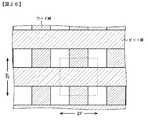
クロスポイント型半導体メモリ装置におけるワード線、ビット線、メモリ部の配置例を、模式的に図26に示す。ワード線とビット線とは、それらの射影像が直交する方向に、ライン・アンド・ストライプ状に配置されている。ワード線、ビット線、及び、ワード線とビット線の交点に配置されたメモリ部から構成された1つのメモリセルの大きさの最小値は、4F2である。ここで、「F」は、クロスポイント型半導体メモリ装置の製造に用いられる製造プロセスのデザインルールで規定される最小加工寸法(製造プロセスの制約上形成し得る最小の線幅寸法及び最小の間隔寸法)を意味する。尚、最小加工寸法Fは、通常、フォトリソグラフィの解像能力で制約される寸法である。即ち、ワード線やビット線の幅、及び、配線間隔の最小値が「F」であるが故に、メモリセルの大きさの最小値は4F2となる。FIG. 26 schematically shows an arrangement example of word lines, bit lines, and memory portions in the cross-point type semiconductor memory device. The word line and the bit line are arranged in a line and stripe form in a direction in which their projected images are orthogonal to each other. The minimum value of the size of one memory cell composed of the word line, the bit line, and the memory portion arranged at the intersection of the word line and the bit line is 4F2 . Here, “F” is a minimum processing dimension (minimum line width dimension and minimum spacing dimension that can be formed due to restrictions of the manufacturing process) defined by a design rule of a manufacturing process used for manufacturing a cross-point type semiconductor memory device. ). The minimum processing dimension F is usually a dimension restricted by the resolution of photolithography. That is, the minimum value of the size of the memory cell is 4F2 because the minimum value of the width of the word line or bit line and the minimum value of the wiring interval is “F”.
しかしながら、クロスポイント型半導体メモリ装置にあっても、1つのメモリセルの大きさを4F2を下回る大きさにすることに対する強い要望がある。However, even in the cross-point type semiconductor memory device, there is a strong demand for reducing the size of one memory cell to less than 4F2 .
従って、本発明の目的は、1つのメモリセルの大きさが4F2を下回る大きさである構成、構造を有するクロスポイント型半導体メモリ装置及びその製造方法を提供することにある。Therefore, an object of the present invention is to provide a cross-point type semiconductor memory device having a configuration and structure in which the size of one memory cell is less than 4F2 and a method for manufacturing the same.
上記の目的を達成するための本発明のクロスポイント型半導体メモリ装置は、
(A)第1の方向に延びる複数の第1の配線、
(B)第1の配線とは異なる層に位置し、第1の方向とは異なる第2の方向に延びる複数の第2の配線、及び、
(C)第1の配線と第2の配線とが重複する領域に設けられたメモリ部、
から構成され、
奇数番目の第1の配線と、偶数番目の第1の配線とは、上下方向に異なる層間絶縁層上に配置されている。In order to achieve the above object, a cross-point type semiconductor memory device of the present invention includes:
(A) a plurality of first wires extending in a first direction;
(B) a plurality of second wirings located in a layer different from the first wiring and extending in a second direction different from the first direction; and
(C) a memory portion provided in a region where the first wiring and the second wiring overlap;
Consisting of
The odd-numbered first wirings and the even-numbered first wirings are disposed on different interlayer insulating layers in the vertical direction.
また、上記の目的を達成するための本発明のクロスポイント型半導体メモリ装置の製造方法は、
(A)第1の方向に延びる複数の第1の配線、
(B)第1の配線とは異なる層に位置し、第1の方向とは異なる第2の方向に延びる複数の第2の配線、及び、
(C)第1の配線と第2の配線とが重複する領域に設けられたメモリ部、
から構成され、
奇数番目の第1の配線と、偶数番目の第1の配線とは、上下方向に異なる層間絶縁層上に配置されており、
第1の配線は、第2の配線の下方に位置し、
奇数番目の第1の配線の配置状態、及び、偶数番目の第1の配線の配置状態は、それぞれ、奇数番目若しくは偶数番目の第1の配線の配置ピッチの半分だけ、ずれているクロスポイント型半導体メモリ装置の製造方法であって、
(a)半導体基板に駆動トランジスタを形成した後、
(b)全面に第1の層間絶縁層を形成し、次いで、第1の層間絶縁層上に、奇数番目の駆動トランジスタと電気的に接続された奇数番目の第1の配線を形成し、その後、
(c)全面に第2の層間絶縁層を形成し、次いで、第2の層間絶縁層上に、偶数番目の駆動トランジスタと電気的に接続された偶数番目の第1の配線を形成し、その後、
(d)全面に第3の層間絶縁層を形成し、次いで、
(e)奇数番目の第1の配線の上方に位置する第2の層間絶縁層及び第3の層間絶縁層の部分に第1の開口部を形成した後、第1の開口部の側壁部に第1のサイドウオールを形成することで第1の開口部を縮径し、偶数番目の第1の配線の上方に位置する第3の層間絶縁層の部分に第2の開口部を形成した後、第2の開口部の側壁部に第2のサイドウオールを形成することで第2の開口部を縮径し、第1の開口部内を導電材料で充填することで第1の接続孔を形成し、第2の開口部内を導電材料で充填することで第2の接続孔を形成し、その後、
(f)第1の接続孔及び第2の接続孔を塞ぐように、第3の層間絶縁層の上にメモリ部及び第2の配線を形成する、
各工程から成る。In addition, a manufacturing method of the cross-point type semiconductor memory device of the present invention for achieving the above object
(A) a plurality of first wires extending in a first direction;
(B) a plurality of second wirings located in a layer different from the first wiring and extending in a second direction different from the first direction; and
(C) a memory portion provided in a region where the first wiring and the second wiring overlap;
Consisting of
The odd-numbered first wiring and the even-numbered first wiring are arranged on different interlayer insulating layers in the vertical direction,
The first wiring is located below the second wiring,
The arrangement state of the odd-numbered first wirings and the arrangement state of the even-numbered first wirings are respectively shifted by half the arrangement pitch of the odd-numbered or even-numbered first wirings. A method for manufacturing a semiconductor memory device, comprising:
(A) After forming the driving transistor on the semiconductor substrate,
(B) forming a first interlayer insulating layer on the entire surface, and then forming an odd-numbered first wiring electrically connected to the odd-numbered driving transistor on the first interlayer insulating layer; ,
(C) forming a second interlayer insulating layer on the entire surface, and then forming an even-numbered first wiring electrically connected to the even-numbered driving transistor on the second interlayer insulating layer; ,
(D) forming a third interlayer insulating layer on the entire surface;
(E) After the first opening is formed in the second interlayer insulating layer and the third interlayer insulating layer located above the odd-numbered first wiring, the first opening is formed on the side wall of the first opening. After reducing the diameter of the first opening by forming the first sidewall and forming the second opening in the portion of the third interlayer insulating layer located above the even-numbered first wiring The second side wall is formed on the side wall of the second opening to reduce the diameter of the second opening, and the inside of the first opening is filled with the conductive material to form the first connection hole. And forming the second connection hole by filling the inside of the second opening with a conductive material,
(F) forming a memory portion and a second wiring on the third interlayer insulating layer so as to close the first connection hole and the second connection hole;
It consists of each process.
本発明のクロスポイント型半導体メモリ装置あるいはその製造方法にあっては、奇数番目の第1の配線と、偶数番目の第1の配線とは、上下方向に異なる層間絶縁層上に配置されている。従って、メモリ部を、製造プロセスのデザインルールで規定される最小加工寸法Fのピッチで形成するとき、奇数番目の第1の配線のピッチP1を2Fとすることができるし、偶数番目の第1の配線のピッチP1を2Fとすることができる。即ち、第1の配線を全体として見た場合、第1の配線のピッチをFとすることができる。従って、第1の配線、メモリ部、第2の配線から構成されたメモリセルの大きさを2F2とすることが可能となり、半導体メモリ装置の高密度化を図ることができる。In the cross-point type semiconductor memory device or the manufacturing method thereof according to the present invention, the odd-numbered first wiring and the even-numbered first wiring are arranged on different interlayer insulating layers in the vertical direction. . Therefore, when the memory portion is formed with a pitch of the minimum processing dimension F defined by the design rule of the manufacturing process, the odd-numbered first wiring pitch P1 can be set to 2F, and the even-numbered first number. The pitch P1 ofone wiring can be set to 2F. That is, when the first wiring is viewed as a whole, the pitch of the first wiring can be set to F. Accordingly, the size of the memory cell including the first wiring, the memory portion, and the second wiring can be 2F2, and the density of the semiconductor memory device can be increased.
以下、図面を参照して、実施例に基づき本発明を説明するが、本発明は実施例に限定されるものではなく、実施例における種々の数値や材料は例示である。尚、説明は、以下の順序で行う。
1.本発明のクロスポイント型半導体メモリ装置及び製造方法、全般に関する説明
2.実施例1(本発明のクロスポイント型半導体メモリ装置及び製造方法)
3.実施例2(実施例1の変形)
4.実施例3(実施例1の別の変形、その他)Hereinafter, the present invention will be described based on examples with reference to the drawings. However, the present invention is not limited to the examples, and various numerical values and materials in the examples are examples. The description will be given in the following order.
1. 1. General description of cross-point type semiconductor memory device and manufacturing method according to the present invention Example 1 (Cross-point semiconductor memory device and manufacturing method of the present invention)
3. Example 2 (Modification of Example 1)
4). Example 3 (another modification of Example 1 and others)
[本発明のクロスポイント型半導体メモリ装置及び製造方法、全般に関する説明]
本発明のクロスポイント型半導体メモリ装置あるいはその製造方法において、第1の配線は第1の方向に延び、第2の配線は第2の方向に延びているが、具体的には、第1の配線の射影像と、第2の配線の射影像とは直交していることが好ましい。尚、奇数番目の第1の配線と偶数番目の第1の配線とは、第1の配線の数え方によっては、奇数番目の第1の配線が偶数番目の第1の配線となり、偶数番目の第1の配線が奇数番目の第1の配線となる場合もあり得るが、このような場合にあっては、偶数番目の第1の配線を奇数番目の第1の配線と読み替え、奇数番目の第1の配線を偶数番目の第1の配線と読み替えればよい。同様に、奇数番目の第2の配線と偶数番目の第2の配線とは、第2の配線の数え方によっては、奇数番目の第2の配線が偶数番目の第2の配線となり、偶数番目の第2の配線が奇数番目の第2の配線となる場合もあり得るが、このような場合にあっても、偶数番目の第2の配線を奇数番目の第2の配線と読み替え、奇数番目の第2の配線を偶数番目の第2の配線と読み替えればよい。[Description of Crosspoint Semiconductor Memory Device and Manufacturing Method of the Present Invention, General]
In the cross-point type semiconductor memory device or the manufacturing method thereof according to the present invention, the first wiring extends in the first direction and the second wiring extends in the second direction. It is preferable that the projected image of the wiring and the projected image of the second wiring are orthogonal to each other. Note that the odd-numbered first wiring and the even-numbered first wiring are the odd-numbered first wiring and the even-numbered first wiring depending on how the first wiring is counted. In some cases, the first wiring is the odd-numbered first wiring. In such a case, the even-numbered first wiring is read as the odd-numbered first wiring, and the odd-numbered first wiring is used. The first wiring may be read as the even-numbered first wiring. Similarly, depending on how the second wiring is counted, the odd-numbered second wiring is the even-numbered second wiring, and the odd-numbered second wiring is the even-numbered second wiring. The second wiring may be an odd-numbered second wiring, but even in such a case, the even-numbered second wiring is replaced with the odd-numbered second wiring, The second wiring may be read as an even-numbered second wiring.
本発明のクロスポイント型半導体メモリ装置の製造方法において、工程(e)は、
(e−1)奇数番目の第1の配線の上方に位置する第2の層間絶縁層及び第3の層間絶縁層に第1の開口部を形成する。
(e−2)第1の開口部の側壁部に第1のサイドウオールを形成することで、第1の開口部を縮径する。
(e−3)偶数番目の第1の配線の上方に位置する第3の層間絶縁層に第2の開口部を形成する。
(e−4)第2の開口部の側壁部に第2のサイドウオールを形成することで、第2の開口部を縮径する。
(e−5)第1の開口部内を導電材料で充填することで、第1の接続孔を形成する。
(e−6)第2の開口部内を導電材料で充填することで、第2の接続孔を形成する。
といった6つの工程から構成されているが、これらの工程の実行順序として、
(e−1)→(e−2)→(e−3)→(e−4)→(e−5)→(e−6)
(e−1)→(e−2)→(e−3)→(e−4)→(e−6)→(e−5)
(e−1)→(e−2)→(e−3)→(e−4)→(e−5)及び(e−6)
(e−3)→(e−4)→(e−1)→(e−2)→(e−5)→(e−6)
(e−3)→(e−4)→(e−1)→(e−2)→(e−6)→(e−5)
(e−3)→(e−4)→(e−1)→(e−2)→(e−5)及び(e−6)
(e−1)→(e−2)→(e−5)→(e−3)→(e−4)→(e−6)
(e−3)→(e−4)→(e−6)→(e−1)→(e−2)→(e−5)
を挙げることができる。In the method for manufacturing a cross-point type semiconductor memory device of the present invention, the step (e) includes:
(E-1) A first opening is formed in the second interlayer insulating layer and the third interlayer insulating layer located above the odd-numbered first wiring.
(E-2) The diameter of the first opening is reduced by forming the first sidewall on the side wall of the first opening.
(E-3) A second opening is formed in the third interlayer insulating layer located above the even-numbered first wiring.
(E-4) The diameter of the second opening is reduced by forming the second sidewall on the side wall of the second opening.
(E-5) The first connection hole is formed by filling the first opening with a conductive material.
(E-6) The second connection hole is formed by filling the second opening with a conductive material.
It consists of six processes such as, but as the execution order of these processes,
(E-1) → (e-2) → (e-3) → (e-4) → (e-5) → (e-6)
(E-1) → (e-2) → (e-3) → (e-4) → (e-6) → (e-5)
(E-1) → (e-2) → (e-3) → (e-4) → (e-5) and (e-6)
(E-3) → (e-4) → (e-1) → (e-2) → (e-5) → (e-6)
(E-3) → (e-4) → (e-1) → (e-2) → (e-6) → (e-5)
(E-3) → (e-4) → (e-1) → (e-2) → (e-5) and (e-6)
(E-1) → (e-2) → (e-5) → (e-3) → (e-4) → (e-6)
(E-3) → (e-4) → (e-6) → (e-1) → (e-2) → (e-5)
Can be mentioned.
本発明のクロスポイント型半導体メモリ装置、あるいは、本発明のクロスポイント型半導体メモリ装置の製造方法によって得られるクロスポイント型半導体メモリ装置(以下、これらを総称して、『本発明のクロスポイント型半導体メモリ装置等』と呼ぶ)にあっては、奇数番目の第1の配線の配置状態、及び、偶数番目の第1の配線の配置状態は、それぞれ、奇数番目若しくは偶数番目の第1の配線の配置ピッチ(P1)の半分だけ、ずれている構成とすることができ、更には、奇数番目若しくは偶数番目の第1の配線の配置ピッチ(P1)は、最小加工寸法Fの2倍に相当する構成とすることができる。即ち、奇数番目の第1の配線は、幅が最小加工寸法Fに等しく、第1の配線と第1の配線との間の距離も最小加工寸法Fに等しく、偶数番目の第1の配線も、幅が最小加工寸法Fに等しく、第1の配線と第1の配線との間の距離も最小加工寸法Fに等しい構成とすることが望ましい。あるいは又、本発明のクロスポイント型半導体メモリ装置等にあっては、奇数番目の第1の配線の射影像と偶数番目の第1の配線の射影像とは、重なりが無く、且つ、隙間が無い構成とすることができる。The crosspoint type semiconductor memory device of the present invention or the crosspoint type semiconductor memory device obtained by the method of manufacturing the crosspoint type semiconductor memory device of the present invention (hereinafter collectively referred to as “the crosspoint type semiconductor memory device of the present invention”). In this case, the arrangement state of the odd-numbered first wirings and the arrangement state of the even-numbered first wirings are respectively the odd-numbered or even-numbered first wirings. only half of the arrangement pitch (P1), the deviation can be configurations, furthermore, odd or even-numbered first wiring arrangement pitch (P1) is twice the minimum feature size F A corresponding configuration can be adopted. That is, the odd-numbered first wiring has a width equal to the minimum processing dimension F, the distance between the first wiring and the first wiring is also equal to the minimum processing dimension F, and the even-numbered first wiring also It is desirable that the width is equal to the minimum processing dimension F and the distance between the first wiring and the first wiring is also equal to the minimum processing dimension F. Alternatively, in the cross-point type semiconductor memory device or the like according to the present invention, the projection image of the odd-numbered first wiring and the projection image of the even-numbered first wiring do not overlap and there is no gap. There can be no configuration.
以上に説明した好ましい構成を含む本発明のクロスポイント型半導体メモリ装置等において、第1の配線は、第2の配線の下方に位置し;第2の方向に沿って隣接するメモリ部は、メモリ延在部によって繋がっており;メモリ部及びメモリ延在部から成るメモリ層と第2の配線とは積層構造を有する構成とすることができる。尚、このような構成を、便宜上、『第1の態様に係るクロスポイント型半導体メモリ装置等』と呼ぶ。この場合、メモリ層が下層であり、第2の配線が上層である。 In the cross-point type semiconductor memory device or the like of the present invention including the preferred configuration described above, the first wiring is located below the second wiring; the memory portion adjacent in the second direction is a memory The memory part and the memory layer including the memory extension part and the second wiring may have a stacked structure. Such a configuration is referred to as “a cross-point type semiconductor memory device or the like according to the first aspect” for convenience. In this case, the memory layer is the lower layer and the second wiring is the upper layer.
そして、第1の態様に係るクロスポイント型半導体メモリ装置等は、
各第1の配線に接続され、半導体基板に形成された駆動トランジスタを更に備えており、
駆動トランジスタを覆う第1の層間絶縁層上に、奇数番目の第1の配線が形成されており、
第1の層間絶縁層及び奇数番目の第1の配線を覆う第2の層間絶縁層上に、偶数番目の第1の配線が形成されており、
第2の層間絶縁層及び偶数番目の第1の配線を覆う第3の層間絶縁層上に、メモリ層が形成されており、
奇数番目の第1の配線とメモリ部とは、第2の層間絶縁層及び第3の層間絶縁層に設けられた第1の接続孔を介して接続されており、
偶数番目の第1の配線とメモリ部とは、第3の層間絶縁層に設けられた第2の接続孔を介して接続されている構成とすることができる。そして、このような構成にあっては、メモリ部の構成に依存して、第1の接続孔及び第2の接続孔のそれぞれは、ダイオードとしての機能を有する形態とすることもできるし、第1の接続孔及び第2の接続孔のそれぞれは、単に導電材料で埋め込まれた形態とすることもできる。尚、前者の場合、第1の接続孔及び第2の接続孔のそれぞれは、第1導電型を有する不純物を含む半導体層領域(例えば、p型不純物あるいはn型不純物を含む半導体層領域)、及び、第1導電型とは異なる第2導電型を有する不純物を含む半導体層領域(例えば、n型不純物あるいはp型不純物を含む半導体層領域)から構成されている形態とすることができる。更には、これらの形態を含むこのような構成にあっては、
駆動トランジスタは電界効果トランジスタ(FET)から成り、
駆動トランジスタのチャネル形成領域の幅は、奇数番目若しくは偶数番目の第1の配線の配置ピッチ(具体的には、例えば「2F」)の少なくとも1.5倍(具体的には、例えば、少なくとも「3F」)であり、駆動トランジスタのチャネル形成領域の幅方向は第2の方向と平行であり、
駆動トランジスタの一方のソース/ドレイン領域は、第1の層間絶縁層に設けられた第1の接続部を介して奇数番目の第1の配線に接続され、あるいは又、第1の層間絶縁層及び第2の層間絶縁層に設けられた第2の接続部を介して偶数番目の第1の配線に接続されており(即ち、奇数番目の駆動トランジスタの一方のソース/ドレイン領域は、第1の層間絶縁層に設けられた第1の接続部を介して奇数番目の第1の配線に接続され、偶数番目の駆動トランジスタの一方のソース/ドレイン領域は、第1の層間絶縁層及び第2の層間絶縁層に設けられた第2の接続部を介して偶数番目の第1の配線に接続されており)、
駆動トランジスタの他方のソース/ドレイン領域は、電源に接続され、あるいは又、接地されている形態とすることができる。The cross-point type semiconductor memory device according to the first aspect is
A drive transistor connected to each first wiring and formed on the semiconductor substrate;
An odd-numbered first wiring is formed on the first interlayer insulating layer covering the driving transistor,
The even-numbered first wiring is formed on the second interlayer insulating layer covering the first interlayer insulating layer and the odd-numbered first wiring,
A memory layer is formed on the third interlayer insulating layer covering the second interlayer insulating layer and the even-numbered first wiring,
The odd-numbered first wiring and the memory portion are connected via a first connection hole provided in the second interlayer insulating layer and the third interlayer insulating layer,
The even-numbered first wiring and the memory portion can be connected via a second connection hole provided in the third interlayer insulating layer. In such a configuration, depending on the configuration of the memory unit, each of the first connection hole and the second connection hole can have a function as a diode. Each of the first connection hole and the second connection hole may be simply embedded with a conductive material. In the former case, each of the first connection hole and the second connection hole includes a semiconductor layer region containing an impurity having the first conductivity type (for example, a semiconductor layer region containing a p-type impurity or an n-type impurity), In addition, a semiconductor layer region containing an impurity having a second conductivity type different from the first conductivity type (for example, a semiconductor layer region containing an n-type impurity or a p-type impurity) can be used. Furthermore, in such a configuration including these forms,
The drive transistor consists of a field effect transistor (FET),
The width of the channel formation region of the driving transistor is at least 1.5 times (specifically, for example, at least “2”) of the arrangement pitch (specifically, for example, “2F”) of the odd-numbered or even-numbered first wirings. 3F "), and the width direction of the channel formation region of the driving transistor is parallel to the second direction,
One source / drain region of the driving transistor is connected to an odd-numbered first wiring through a first connection portion provided in the first interlayer insulating layer, or alternatively, the first interlayer insulating layer and It is connected to the even-numbered first wiring via the second connection portion provided in the second interlayer insulating layer (that is, one source / drain region of the odd-numbered driving transistor is connected to the first wiring One source / drain region of the even-numbered driving transistor is connected to the odd-numbered first wiring through the first connection portion provided in the interlayer insulating layer, and the first source / drain region of the even-numbered driving transistor Are connected to the even-numbered first wirings through the second connection portion provided in the interlayer insulating layer),
The other source / drain region of the driving transistor may be connected to a power source or grounded.
更には、以上に説明した好ましい構成、形態を含む本発明のクロスポイント型半導体メモリ装置等において、奇数番目の第2の配線と、偶数番目の第2の配線とは、上下方向に異なる層間絶縁層上に配置されている形態とすることができる。尚、このような形態を、便宜上、『第2の態様に係るクロスポイント型半導体メモリ装置等』と呼ぶ。そして、第2の態様に係るクロスポイント型半導体メモリ装置等にあっては、奇数番目の第2の配線の配置状態、及び、偶数番目の第2の配線の配置状態は、それぞれ、奇数番目若しくは偶数番目の第2の配線の配置ピッチ(P2)の半分だけ、ずれている構成とすることができ、更には、奇数番目若しくは偶数番目の第2の配線の配置ピッチ(P2)は、最小加工寸法Fの2倍に相当する構成とすることができる。即ち、奇数番目の第2の配線は、幅が最小加工寸法Fに等しく、第2の配線と第2の配線との間の距離も最小加工寸法Fに等しく、偶数番目の第2の配線も、幅が最小加工寸法Fに等しく、第2の配線と第2の配線との間の距離も最小加工寸法Fに等しい構成とすることが望ましい。あるいは又、第2の態様に係るクロスポイント型半導体メモリ装置等にあっては、奇数番目の第2の配線の射影像と偶数番目の第2の配線の射影像とは、重なりが無く、且つ、隙間が無い構成とすることができる。Furthermore, in the cross-point type semiconductor memory device of the present invention including the preferred configuration and configuration described above, the odd-numbered second wiring and the even-numbered second wiring are different in the vertical direction. It can be set as the form arrange | positioned on the layer. Such a configuration is referred to as “a cross-point type semiconductor memory device or the like according to a second embodiment” for convenience. In the cross-point type semiconductor memory device or the like according to the second aspect, the odd-numbered second wiring arrangement state and the even-numbered second wiring arrangement state are odd-numbered or The arrangement pitch may be shifted by half the even-numbered second wiring arrangement pitch (P2 ). Furthermore, the odd-numbered or even-numbered second wiring arrangement pitch (P2 ) is: A configuration corresponding to twice the minimum processing dimension F can be adopted. That is, the odd-numbered second wiring has a width equal to the minimum processing dimension F, the distance between the second wiring and the second wiring is also equal to the minimum processing dimension F, and the even-numbered second wiring also It is desirable that the width is equal to the minimum processing dimension F, and the distance between the second wiring and the second wiring is also equal to the minimum processing dimension F. Alternatively, in the cross-point type semiconductor memory device or the like according to the second aspect, the projection image of the odd-numbered second wiring and the projection image of the even-numbered second wiring do not overlap, and It can be set as the structure without a clearance gap.
以上に説明した好ましい構成を含む第2の態様に係るクロスポイント型半導体メモリ装置等において、第1の配線は、第2の配線の下方に位置し;第2の方向に沿って隣接するメモリ部は、メモリ延在部によって繋がっている構成とすることができる。尚、メモリ部及びメモリ延在部からメモリ層が構成される。 In the cross-point type semiconductor memory device or the like according to the second aspect including the preferred configuration described above, the first wiring is located below the second wiring; the memory section adjacent in the second direction Can be configured to be connected by a memory extension. A memory layer is composed of the memory part and the memory extension part.
尚、以上に説明した好ましい構成を含む第2の態様に係るクロスポイント型半導体メモリ装置等にあっては、
メモリ層上に奇数番目の第2の配線が形成されており、
奇数番目の第2の配線及び第3の層間絶縁層を覆う第4の層間絶縁層上に、第2のメモリ層及び偶数番目の第2の配線が形成されており、
第2のメモリ層から構成されたメモリ部は、第4の層間絶縁層、第3の層間絶縁層及び第2の層間絶縁層に設けられた第3の接続孔を介して奇数番目の第1の配線に接続され、また、第2のメモリ層から構成されたメモリ部は、第4の層間絶縁層及び第3の層間絶縁層に設けられた第4の接続孔を介して偶数番目の第1の配線に接続されている構成とすることができる。そして、このような構成にあっては、メモリ部の構成に依存して、第3の接続孔及び第4の接続孔のそれぞれは、ダイオードとしての機能を有する構成とすることもできるし、第3の接続孔及び第4の接続孔のそれぞれは、単に導電材料で埋め込まれた構成とすることもできる。尚、前者の場合、第3の接続孔及び第4の接続孔のそれぞれは、第1導電型を有する不純物を含む半導体層領域(例えば、p型不純物あるいはn型不純物を含む半導体層領域)、及び、第1導電型とは異なる第2導電型を有する不純物を含む半導体層領域(例えば、n型不純物あるいはp型不純物を含む半導体層領域)から構成されている形態とすることができる。In the cross-point type semiconductor memory device or the like according to the second aspect including the preferred configuration described above,
An odd-numbered second wiring is formed on the memory layer,
A second memory layer and an even-numbered second wiring are formed on the fourth interlayer insulating layer covering the odd-numbered second wiring and the third interlayer insulating layer;
The memory section composed of the second memory layer has an odd first number through the third connection hole provided in the fourth interlayer insulating layer, the third interlayer insulating layer, and the second interlayer insulating layer. In addition, the memory portion formed of the second memory layer is connected to the wirings of the first and second wiring layers through the fourth connection holes provided in the fourth interlayer insulating layer and the third interlayer insulating layer. It can be set as the structure connected to 1 wiring. In such a configuration, depending on the configuration of the memory unit, each of the third connection hole and the fourth connection hole may have a function as a diode. Each of the three connection holes and the fourth connection hole may be simply embedded with a conductive material. In the former case, each of the third connection hole and the fourth connection hole includes a semiconductor layer region containing an impurity having the first conductivity type (for example, a semiconductor layer region containing a p-type impurity or an n-type impurity), In addition, a semiconductor layer region containing an impurity having a second conductivity type different from the first conductivity type (for example, a semiconductor layer region containing an n-type impurity or a p-type impurity) can be used.
ここで、第3の接続孔は、偶数番目の第2の配線を形成すべき部分と奇数番目の第1の配線との間に位置する第2の層間絶縁層、第3の層間絶縁層及び第4の層間絶縁層の部分に第3の開口部を形成した後、第3の開口部の側壁部に第3のサイドウオールを形成することで第3の開口部を縮径し、第3の開口部内を導電材料で充填することで第3の接続孔を形成するといった方法で得ることができる。また、第4の接続孔は、偶数番目の第2の配線を形成すべき部分と偶数番目の第1の配線との間に位置する第3の層間絶縁層及び第4の層間絶縁層の部分に第4の開口部を形成した後、第4の開口部の側壁部に第4のサイドウオールを形成することで第4の開口部を縮径し、第4の開口部内を導電材料で充填することで第4の接続孔を形成するといった方法で得ることができる。 Here, the third connection hole includes a second interlayer insulating layer, a third interlayer insulating layer, which are located between a portion where the even-numbered second wiring is to be formed and the odd-numbered first wiring. After the third opening is formed in the fourth interlayer insulating layer, the third opening is reduced in diameter by forming a third sidewall on the side wall of the third opening, The third connection hole is formed by filling the inside of the opening with a conductive material. The fourth connection hole is a portion of the third interlayer insulating layer and the fourth interlayer insulating layer located between the portion where the even-numbered second wiring is to be formed and the even-numbered first wiring. After the fourth opening is formed, the diameter of the fourth opening is reduced by forming a fourth sidewall on the side wall of the fourth opening, and the inside of the fourth opening is filled with a conductive material. By doing so, it can be obtained by a method of forming the fourth connection hole.
以上に説明した各種の好ましい構成、形態を含む本発明のクロスポイント型半導体メモリ装置等において、第1の配線、メモリ部、及び、第2の配線によって、相変化型メモリ(PRAM)が構成されている形態とすることができる。ここで、係る形態にあっては、メモリ部(メモリ層や第2のメモリ層)を、具体的には、GeSbTe、ZnSe、GaSnTe等の金属とSeやTeとの化合物であるカルコゲナイド等から構成することができる。あるいは又、巨大磁気抵抗変化効果(CMR効果)を有する材料からメモリ部(メモリ層や第2のメモリ層)を構成することができ、この場合、係る材料としてPrCaMnO3を挙げることができる。あるいは又、金属を含むイオン導電体からメモリ部(メモリ層や第2のメモリ層)を構成する場合、係る材料として、Cu、Ag、Znから選ばれるいずれかの元素と、Te、S、Seといったカルコゲナイド元素から選ばれるいずれかの元素とが含まれている導電性又は半導電性の薄膜(例えば、GeSbTe、GeTe、GeSe、GeS、SiGeTe、SiGeSbTeから成る薄膜や、これらの薄膜と、例えば、Ag、Ag合金、Cu、Cu合金、Zn、Zn合金から成る薄膜の積層構造)から構成することができるし、あるいは又、全体あるいは膜厚方向の一部分に、希土類元素のうち、La、Ce、Pr、Nd、Sm、Eu、Gd、Tb、Dy、Ho、Er、Yb、Yから選ばれる、1種類、若しくは、複数種類の希土類元素の酸化物からなる膜(希土類酸化物薄膜)や、Hf、Ta、W等の酸化膜が形成された構成とすることができる。In the cross-point type semiconductor memory device of the present invention including various preferable configurations and forms described above, a phase change memory (PRAM) is configured by the first wiring, the memory unit, and the second wiring. It can be set as a form. Here, in such a form, the memory unit (memory layer or second memory layer) is specifically composed of a metal such as GeSbTe, ZnSe, or GaSnTe and a chalcogenide that is a compound of Se or Te. can do. Alternatively, the memory portion (memory layer or second memory layer) can be formed from a material having a giant magnetoresistance change effect (CMR effect). In this case, PrCaMnO3 can be used as the material. Alternatively, when the memory portion (memory layer or second memory layer) is formed from an ion conductor containing metal, any one of elements selected from Cu, Ag, and Zn, and Te, S, Se are used as the material. A conductive or semiconductive thin film containing any element selected from chalcogenide elements such as GeSbTe, GeTe, GeSe, GeS, SiGeTe, SiGeSbTe, and these thin films, for example, Or a thin film layered structure of Ag, Ag alloy, Cu, Cu alloy, Zn, Zn alloy), or, among the rare earth elements, La, Ce, One or more kinds of rare earth elements selected from Pr, Nd, Sm, Eu, Gd, Tb, Dy, Ho, Er, Yb, Y It can be film made of oxide (rare earth oxide thin film) and, Hf, Ta, a structure in which oxide films of W or the like is formed.
本発明のクロスポイント型半導体メモリ装置等において、第1の配線、第2の配線を構成する材料として、例えば、タングステン(W)、TiN、アルミニウム(Al)、銅(Cu)、モリブデン(Mo)、チタン(Ti)、タンタル(Ta)、TiW、WN、シリサイドを例示することができる。尚、配線を例えばタングステン(W)から構成する場合、その下に、Ti層やTiN層から成る密着層を形成してもよい。一方、配線を下層導電材料層及び上層導電材料層の積層構造から構成する場合、下層導電材料層をシリコン層(例えば、多結晶シリコン層やアモルファスシリコン層)から構成し、上層導電材料層を、ニッケルシリサイド層、ニッケル・白金シリサイド層、コバルトシリサイド層、チタンシリサイド層から構成とすることができる。また、層間絶縁層(第1の層間絶縁層、第2の層間絶縁層、第3の層間絶縁層、第4の層間絶縁層)を構成する材料として、SiO2、NSG(ノンドープ・シリケート・ガラス)、BPSG(ホウ素・リン・シリケート・ガラス)、PSG等のSiOX系材料、SiN、SiON等のSiNY系材料、低誘電率絶縁材料(例えば、SiOC、SiOF、フルオロカーボン)を例示することができる。サイドウオールを構成する材料も、これらの絶縁材料から構成すればよいが、層間絶縁層とはエッチング選択比のある材料を選択する必要がある。In the cross-point type semiconductor memory device or the like of the present invention, as materials constituting the first wiring and the second wiring, for example, tungsten (W), TiN, aluminum (Al), copper (Cu), molybdenum (Mo) Titanium (Ti), tantalum (Ta), TiW, WN, and silicide can be exemplified. When the wiring is made of, for example, tungsten (W), an adhesion layer made of a Ti layer or a TiN layer may be formed thereunder. On the other hand, when the wiring is composed of a laminated structure of a lower conductive material layer and an upper conductive material layer, the lower conductive material layer is composed of a silicon layer (for example, a polycrystalline silicon layer or an amorphous silicon layer), and the upper conductive material layer is A nickel silicide layer, a nickel / platinum silicide layer, a cobalt silicide layer, and a titanium silicide layer can be used. Further, as a material constituting the interlayer insulating layer (first interlayer insulating layer, second interlayer insulating layer, third interlayer insulating layer, fourth interlayer insulating layer), SiO2 , NSG (non-doped silicate glass) ), BPSG (boron phosphorus silicate glass), SiOX based materials such as PSG, SiN, SiNY-based material such as SiON, a low dielectric constant insulating material (e.g., SiOC, SiOF, be exemplified fluorocarbon) it can. The material constituting the sidewall may be made of any of these insulating materials, but it is necessary to select a material having an etching selectivity with respect to the interlayer insulating layer.
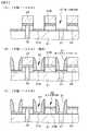
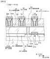
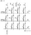
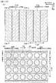
実施例1は、本発明のクロスポイント型半導体メモリ装置及びその製造方法に関し、具体的には、第1の態様に係るクロスポイント型半導体メモリ装置等に関する。実施例1のクロスポイント型半導体メモリ装置の第2の方向に沿った模式的な一部断面図を図4及び図5に示し、第1の方向に沿った模式的な一部断面図を図6及び図7に示す。また、奇数番目の第1の配線、偶数番目の第1の配線及び第2の配線の配置状態を模式的に図10の(A)に示し、実施例1のクロスポイント型半導体メモリ装置を上から眺めた模式図を図10の(B)に示す。更には、実施例1のクロスポイント型半導体メモリ装置の等価回路図を図11に示し、実施例1のクロスポイント型半導体メモリ装置における駆動トランジスタの配置状態を説明するための模式図を図12に示す。尚、図4は、図10の(A)の矢印A−Aに沿った模式的な一部断面図であり、図5は、図10の(A)の矢印B−Bに沿った模式的な一部断面図であり、図6は、図10の(A)の矢印C−Cに沿った模式的な一部断面図であり、図7は、図10の(A)の矢印D−Dに沿った模式的な一部断面図である。また、図10の(A)及び(B)において、奇数番目の第1の配線、偶数番目の第1の配線及び第2の配線を明示するために、これらの配線に斜線を付した。更には、図10の(B)において、メモリ部を明示するために、メモリ部に相当する箇所の外縁を円形で示した。図12においては、8本の奇数番目の第1の配線、8本の偶数番目の第1の配線、16本の第2の配線(即ち16×16個のメモリセル)を示している。ここで、第2の方向に延びるゲート電極91A(後述する)に斜線を付している。尚、クロスポイント型半導体メモリ装置において、複数のメモリセルが設けられている領域を、メモリセルアレイ領域と呼ぶ場合がある。 Example 1 relates to a cross-point type semiconductor memory device and a manufacturing method thereof according to the present invention, and specifically relates to a cross-point type semiconductor memory device according to a first aspect. FIG. 4 and FIG. 5 show schematic partial cross-sectional views along the second direction of the cross-point type semiconductor memory device of Example 1, and FIG. 4 shows schematic partial cross-sectional views along the first direction. 6 and FIG. Further, the arrangement state of the odd-numbered first wiring, the even-numbered first wiring, and the second wiring is schematically shown in FIG. 10A, and the cross-point type semiconductor memory device of the first embodiment is FIG. 10B shows a schematic view viewed from above. Furthermore, an equivalent circuit diagram of the cross-point type semiconductor memory device of the first embodiment is shown in FIG. 11, and a schematic diagram for explaining the arrangement state of the drive transistors in the cross-point type semiconductor memory device of the first embodiment is shown in FIG. Show. 4 is a schematic partial sectional view taken along the arrow AA in FIG. 10A, and FIG. 5 is a schematic view taken along the arrow BB in FIG. FIG. 6 is a schematic partial sectional view taken along the arrow CC in FIG. 10A, and FIG. 7 is an arrow D- in FIG. It is a typical partial sectional view along D. Further, in FIGS. 10A and 10B, in order to clearly indicate the odd-numbered first wiring, the even-numbered first wiring, and the second wiring, these wirings are hatched. Further, in FIG. 10B, the outer edge of the portion corresponding to the memory portion is shown by a circle in order to clearly indicate the memory portion. FIG. 12 shows eight odd-numbered first wirings, eight even-numbered first wirings, and sixteen second wirings (that is, 16 × 16 memory cells). Here, the
実施例1のクロスポイント型半導体メモリ装置は、
(A)第1の方向に延びる複数の第1の配線(所謂ワード線)41A,41B、
(B)第1の配線41A,41Bとは異なる層(具体的には、素子断面あるいはメモリ部断面垂直方向に異なる層)に位置し、第1の方向とは異なる第2の方向に延びる複数の第2の配線(所謂ビット線)42、及び、
(C)第1の配線41A,41Bと第2の配線42とが重複する領域に設けられたメモリ部43、
から構成されており、
奇数番目の第1の配線41Aと、偶数番目の第1の配線41Bとは、上下方向に異なる層間絶縁層21,22上に配置されている。The cross-point type semiconductor memory device of Example 1 is
(A) A plurality of first wirings (so-called word lines) 41A, 41B extending in the first direction,
(B) A plurality of layers extending in a second direction different from the first direction, located in a layer different from the
(C) a
Consists of
The odd-numbered
尚、1つのメモリセル(メモリ素子)は、1本の第1の配線41A,41B、1本の第2の配線42、及び、これらの1本の第1の配線41A,41Bと1本の第2の配線42によって挟まれたメモリ部43から構成されている。 One memory cell (memory element) includes one
ここで、実施例1のクロスポイント型半導体メモリ装置、あるいは、後述する実施例1のクロスポイント型半導体メモリ装置の製造方法によって得られるクロスポイント型半導体メモリ装置(以下、これらを総称して、『実施例1のクロスポイント型半導体メモリ装置等』と呼ぶ)にあっては、奇数番目の第1の配線41Aの配置状態、及び、偶数番目の第1の配線41Bの配置状態は、それぞれ、奇数番目若しくは偶数番目の第1の配線の配置ピッチ(P1)の半分だけ、ずれている。尚、奇数番目若しくは偶数番目の第1の配線41A,41Bの配置ピッチP1は、最小加工寸法Fの2倍に相当する。即ち、ライン・アンド・ストライプ状に配置された奇数番目の第1の配線41Aは、幅が最小加工寸法Fに等しく、第1の配線41Aと第1の配線41Aとの間の距離も最小加工寸法Fに等しい。また、ライン・アンド・ストライプ状に配置された偶数番目の第1の配線41Bも、幅が最小加工寸法Fに等しく、第1の配線41Bと第1の配線41Bとの間の距離も最小加工寸法Fに等しい。あるいは又、実施例1のクロスポイント型半導体メモリ装置等にあっては、奇数番目の第1の配線41Aの射影像と偶数番目の第1の配線41Bの射影像とは、重なりが無く、且つ、隙間が無い(図10の(A)参照)。また、ライン・アンド・ストライプ状に配置された第2の配線42は、幅が最小加工寸法Fに等しく、第2の配線42と第2の配線42との間の距離も最小加工寸法Fに等しい。ここで、第1の配線41A,41Bの射影像と、第2の配線42の射影像とは、直交している。Here, the cross-point type semiconductor memory device of the first embodiment or the cross-point type semiconductor memory device obtained by the method of manufacturing the cross-point type semiconductor memory device of the first embodiment described later (hereinafter collectively referred to as “ In the first embodiment, the arrangement state of the odd-numbered
また、実施例1にあっては、第1の配線41A,41Bは、第2の配線42の下方に位置している。そして、第2の方向に沿って隣接するメモリ部43は、メモリ延在部44によって繋がっている。更には、メモリ部43及びメモリ延在部44から成るメモリ層45と第2の配線42とは積層構造を有する。尚、メモリ層45が下層であり、第2の配線42が上層である。 In the first embodiment, the first wirings 41 </ b> A and 41 </ b> B are located below the
更には、各第1の配線41A,41Bに接続され、半導体基板11に形成された駆動トランジスタ91、及び、各第2の配線42に接続され、半導体基板11に形成された周辺回路用トランジスタ92を備えている。尚、周辺回路用トランジスタ92は、図示しない周辺回路部に設けられている。そして、駆動トランジスタ91を覆う第1の層間絶縁層21上に、奇数番目の第1の配線41Aが形成されており、第1の層間絶縁層21及び奇数番目の第1の配線41Aを覆う第2の層間絶縁層22上に、偶数番目の第1の配線41Bが形成されており、第2の層間絶縁層22及び偶数番目の第1の配線41Bを覆う第3の層間絶縁層23上にメモリ層45が形成されている。ここで、奇数番目の第1の配線41Aとメモリ部43とは、第2の層間絶縁層22及び第3の層間絶縁層23に設けられた第1の接続孔71を介して接続されており、偶数番目の第1の配線41Bとメモリ部43とは、第3の層間絶縁層23に設けられた第2の接続孔72を介して接続されている。そして、第1の接続孔71及び第2の接続孔72のそれぞれは、ダイオードとしての機能を有する。具体的には、第1の接続孔71及び第2の接続孔72のそれぞれは、第1導電型を有する不純物を含む半導体層領域(具体的には、p型不純物を含む半導体層領域82A)、及び、第1導電型とは異なる第2導電型を有する不純物を含む半導体層領域(具体的には、n型不純物を含む半導体層領域81A)から構成されている。ここで、第1の接続孔71及び第2の接続孔72のそれぞれが、ダイオードとしての機能を有していない場合、図11に示す、駆動トランジスタ91A及び周辺回路用駆動トランジスタ92Aをオン状態として、メモリセルMC1を選択したとき、例えば、メモリセルMC2,MC3,MC4といった経路を介して電流が流れてしまうことを防止することができなくなる。Further, the driving
駆動トランジスタ91は電界効果トランジスタ(FET)から成り、駆動トランジスタ91のチャネル形成領域91Dの幅は、例えば、奇数番目若しくは偶数番目の第1の配線41A,41Bの配置ピッチP1の1.5倍(=3F)であり、駆動トランジスタ91のチャネル形成領域91Dの幅方向は第2の方向と平行である。そして、駆動トランジスタ91の一方のソース/ドレイン領域91Bは、第1の層間絶縁層21に設けられた第1の接続部31を介して奇数番目の第1の配線41Aに接続され、あるいは又、第1の層間絶縁層21及び第2の層間絶縁層22に設けられた第2の接続部32を介して偶数番目の第1の配線41Bに接続されている。更には、駆動トランジスタ91の他方のソース/ドレイン領域91Cは、実施例1にあっては、接地されている。ここで、接地線との接続はメモリセルアレイ領域の周辺部で行われており、図示していない。尚、参照番号91Eはゲート絶縁膜である。このようにチャネル形成領域91Dの幅を配置ピッチP1の1.5倍とすることで、駆動トランジスタの駆動能力の増加を図ることができる。また、駆動トランジスタがメモリセルの下方に設けられているので、即ち、駆動トランジスタがメモリセルアレイ領域に設けられているので、周辺回路部の占有面積を減少させることができる。このような駆動トランジスタ91の配置を可能にするために、図12に示すように、駆動トランジスタの配列を複数のグループA,B,C,Dに分けて、それぞれのグループでは配置ピッチ4F毎に駆動トランジスタ91を配置し、アレイ全体ではこれらのグループを4回繰り返すことで、全第1の配線に対して駆動トランジスタ91を配置できる。The
尚、図12においては、チャネル形成領域91Dが占める領域を「×」印で示し、第1の接続部31をアルファベット「A」を囲む丸印で示し、第2の接続部32をアルファベット「B」を囲む丸印で示している。そして、接続部は、4本の第1の配線毎に、1本の第2の配線分、ずらして設けられている。即ち、(16本の第1の配線)×(4本の第2の配線)毎に、4つの駆動トランジスタ91が設けられている。 In FIG. 12, the region occupied by the
実施例1のクロスポイント型半導体メモリ装置等において、メモリセルは、相変化型メモリ(PRAM)から構成されている。即ち、実施例1にあっては、メモリ部を構成する相変化材料がアモルファス状態と結晶状態とで電気抵抗が数桁違うことを利用して、不揮発性メモリとして動作させる。具体的には、メモリ部に短時間、パルス状の大電流(例えば、200マイクロアンペア,20ナノ秒)を流した後、急冷すると、メモリ部を構成する相変化材料はアモルファス状態となり、高抵抗を示す。一方、メモリ部に比較的長時間、パルス状の小電流(例えば、100マイクロアンペア,100ナノ秒)を流した後、徐冷すると、メモリ部を構成する相変化材料は結晶状態となり、低抵抗を示す。メモリ部43あるいはメモリ層45をカルコゲナイド系材料から構成したが、これに限定するものではなく、例えば、巨大磁気抵抗変化効果(CMR効果)を有する材料から構成することもできる。 In the cross-point type semiconductor memory device or the like of the first embodiment, the memory cell is composed of a phase change type memory (PRAM). That is, in the first embodiment, the phase change material constituting the memory unit is operated as a nonvolatile memory by utilizing the fact that the electrical resistance is different by several orders of magnitude between the amorphous state and the crystalline state. Specifically, when a large pulse current (for example, 200 microamperes, 20 nanoseconds) is passed through the memory portion for a short time and then rapidly cooled, the phase change material constituting the memory portion becomes an amorphous state and has a high resistance. Indicates. On the other hand, when a small pulse current (for example, 100 microamperes, 100 nanoseconds) is passed through the memory portion for a relatively long time and then slowly cooled, the phase change material constituting the memory portion becomes a crystalline state and has low resistance. Indicates. The
例えば、メモリセルMC1に記憶されたデータ(具体的には、メモリセルMC1を構成するメモリ部の抵抗値)を読み出す場合、メモリセルMC1に接続された周辺回路用トランジスタ92Aをオン状態とし、第2の配線42に所定の電圧Vbを印加し、他の周辺回路用トランジスタ92をオフ状態とする。更には、メモリセルMC1に接続された駆動トランジスタ91Aをオン状態とし、他の駆動トランジスタ91をオフ状態とする。こうして、周辺回路用駆動トランジスタ92から駆動トランジスタ91へと電流を流す。その結果、周辺回路用駆動トランジスタ92A、メモリセルMC1を構成するメモリ部43、ダイオード、駆動トランジスタ91Aを経由して、電流が流れ、メモリ部43の抵抗値が高抵抗か低抵抗かを知ることができ、記憶された情報を読み出すことができる。メモリセルMC1への情報の書き込みも、流す電流の値、パルス値を適切に選択して、実質的に同様の方法とすればよい。For example, when reading data stored in the memory cell MC1 (specifically, the resistance value of the memory portion constituting the memory cell MC1 ), the
尚、図示していないが、1本の第1の配線41A,41Bのそれぞれに2つ以上の駆動トランジスタ91を接続し、1本の第2の配線42に2つ以上の周辺回路用トランジスタ92を接続することで、第1の配線41A,41B、第2の配線42の電位を急速に接地電位とする構成としてもよい。 Although not shown, two or
以下、第1の層間絶縁層等の模式的な一部端面図である図1の(A)〜(C)、図2の(A)〜(C)、図3の(A)〜(C)、図4〜図7、各種配線や開口部等の配置を模式的に示す図8の(A)〜(B)、図9の(A)〜(B)、図10の(A)〜(B)を参照して、実施例1のクロスポイント型半導体メモリ装置の製造方法を説明する。尚、図1の(A)〜(C)、図2の(A)〜(C)、図3の(A)〜(C)、あるいは、後述する図13の(A)〜(C)、図14の(A)〜(B)において、第1の接続部31及び第2の接続部32は、実際には、第2の配線等と同じ断面内に位置してはいないが、便宜上、同じ端面図内で示している。 Hereinafter, FIGS. 1A to 1C, FIGS. 2A to 2C, and FIGS. 3A to 3C are schematic partial end views of the first interlayer insulating layer and the like. 4 to 7, FIGS. 8A to 8B schematically showing the arrangement of various wirings and openings, FIGS. 9A to 9B, and FIGS. With reference to (B), a method for manufacturing the cross-point type semiconductor memory device of the first embodiment will be described. 1 (A) to (C), FIG. 2 (A) to (C), FIG. 3 (A) to (C), or FIG. 13 (A) to (C) described later, In FIGS. 14A to 14B, the
ここで、実施例1のクロスポイント型半導体メモリ装置の製造方法によって得られるクロスポイント型半導体メモリ装置にあっては、第1の配線41A,41Bは、第2の配線42の下方に位置し、奇数番目の第1の配線41Aの配置状態、及び、偶数番目の第1の配線41Bの配置状態は、それぞれ、奇数番目若しくは偶数番目の第1の配線の配置ピッチ(P1)の半分だけ、ずれている。また、第2の方向に沿って隣接するメモリ部43は、メモリ延在部44によって繋がっており、メモリ部43上(メモリ部43の上方を含む)に第2の配線42が形成されている。Here, in the cross-point type semiconductor memory device obtained by the method for manufacturing the cross-point type semiconductor memory device of the first embodiment, the
[工程−100]
先ず、シリコン半導体基板から成る半導体基板11に、駆動トランジスタ(FET)91及び周辺回路用トランジスタ(FET)92を含む周辺回路を構成するトランジスタを、周知の方法で形成する。尚、駆動トランジスタ91は、図4〜図7及び図12に模式図を示すように、ゲート電極91A、ソース/ドレイン領域91B,91Cから構成されている。ここで、参照番号12は素子分離領域である。[Step-100]
First, a transistor constituting a peripheral circuit including a driving transistor (FET) 91 and a peripheral circuit transistor (FET) 92 is formed on a
[工程−110]
その後、SiO2から成る第1の層間絶縁層21をCVD法に基づき全面に形成し、化学的機械的研磨法(CMP法)等に基づき第1の層間絶縁層21を平坦化する。次いで、第1の層間絶縁層21上に、奇数番目の駆動トランジスタ91と電気的に接続された奇数番目の第1の配線41Aを形成する。具体的には、例えば、奇数番目の駆動トランジスタ91の一方のソース/ドレイン領域91Bの上方に位置する第1の層間絶縁層21の部分に、フォトリソグラフィ技術及びドライエッチング技術に基づき開口を形成した後、係る開口を導電材料で埋め込むことで第1の接続部31を形成する。次いで、第1の接続部31上を含む第1の層間絶縁層21上に、スパッタリング法に基づき、Ti層やTiN層から成る密着層(図示せず)及びタングステン(W)から成る導電材料層を成膜した後、フォトリソグラフィ技術及びドライエッチング技術に基づき係る導電材料層及び密着層をパターニングすることで、第1の方向(図面の紙面垂直方向)に延びる奇数番目の第1の配線41Aを形成する。こうして、図1の(A)及び図8の(A)に示す構造を得ることができる。尚、図8の(A)においては、奇数番目の第1の配線41Aを明示するために、奇数番目の第1の配線41Aに斜線を付した。[Step-110]
Thereafter, a first
[工程−120]
その後、SiO2から成る第2の層間絶縁層22をCVD法に基づき全面に形成し、次いで、第2の層間絶縁層22上に、偶数番目の駆動トランジスタ91と電気的に接続された偶数番目の第1の配線41Bを形成する。具体的には、例えば、偶数番目の駆動トランジスタ91の一方のソース/ドレイン領域91Bの上方に位置する第1の層間絶縁層21及び第2の層間絶縁層22の部分に、フォトリソグラフィ技術及びドライエッチング技術に基づき開口を形成した後、係る開口を導電材料で埋め込むことで第2の接続部32を形成する。次いで、第2の接続部32上を含む第2の層間絶縁層22上に、スパッタリング法に基づき、Ti層やTiN層から成る密着層(図示せず)及びタングステン(W)から成る導電材料層を成膜した後、フォトリソグラフィ技術及びドライエッチング技術に基づき係る導電材料層及び密着層をパターニングすることで、第1の方向に延びる偶数番目の第1の配線41Bを形成する。こうして、図1の(B)及び図8の(B)に示す構造を得ることができる。尚、図8の(B)においては、偶数番目の第1の配線41Bを明示するために、偶数番目の第1の配線41Bに斜線を付した。[Step-120]
Thereafter, asecond
[工程−130]
その後、SiO2から成る第3の層間絶縁層23をCVD法に基づき全面に形成する(図1の(C)参照)。[Step-130]
Thereafter, a third
[工程−140]
次に、奇数番目の第1の配線41Aの上方に位置する第2の層間絶縁層22及び第3の層間絶縁層23の部分に第1の開口部51を形成した後、第1の開口部51の側壁部に第1のサイドウオール61を形成することで第1の開口部51を縮径し、偶数番目の第1の配線41Bの上方に位置する第3の層間絶縁層23の部分に第2の開口部52を形成した後、第2の開口部52の側壁部に第2のサイドウオール62を形成することで第2の開口部52を縮径し、第1の開口部51内を導電材料で充填することで第1の接続孔71を形成し、第2の開口部52内を導電材料で充填することで第2の接続孔72を形成する。即ち、この[工程−140]は、
(e−1)奇数番目の第1の配線41Aの上方に位置する第2の層間絶縁層22及び第3の層間絶縁層23に第1の開口部51を形成する。
(e−2)第1の開口部51の側壁部に第1のサイドウオール61を形成することで、第1の開口部51を縮径する。
(e−3)偶数番目の第1の配線41Bの上方に位置する第3の層間絶縁層23に第2の開口部52を形成する。
(e−4)第2の開口部52の側壁部に第2のサイドウオール62を形成することで、第2の開口部52を縮径する。
(e−5)第1の開口部51内を導電材料で充填することで、第1の接続孔71を形成する。
(e−6)第2の開口部52内を導電材料で充填することで、第2の接続孔72を形成する。
といった6つの工程から構成されているが、これらの工程の実行順序として、実施例1にあっては、
(e−1)→(e−2)→(e−3)→(e−4)→(e−5)及び(e−6)
を採用している。[Step-140]
Next, after the
(E-1) A
(E-2) The diameter of the
(E-3) A
(E-4) The diameter of the
(E-5) The
(E-6) The
In the first embodiment, the execution order of these steps is as follows:
(E-1) → (e-2) → (e-3) → (e-4) → (e-5) and (e-6)
Is adopted.
[工程−140A]
即ち、先ず、奇数番目の第1の配線41Aの上方に位置する第2の層間絶縁層22及び第3の層間絶縁層23の部分に第1の開口部51を形成した後、第1の開口部51の側壁部に第1のサイドウオール61を形成することで、第1の開口部51を縮径する。具体的には、フォトリソグラフィ技術及びドライエッチング技術に基づき、奇数番目の第1の配線41Aの上方に位置する第2の層間絶縁層22及び第3の層間絶縁層23の部分に第1の開口部51を形成する(図2の(A)参照)。その後、第1の開口部51を含む全面に、CVD法に基づきSiNから成るサイドウオール層を形成し、係るサイドウオール層をエッチバックする。こうして、図2の(B)及び図9の(A)に示す構造を得ることができる。[Step-140A]
That is, first, after the
[工程−140B]
その後、偶数番目の第1の配線41Bの上方に位置する第3の層間絶縁層23の部分に第2の開口部52を形成した後、第2の開口部52の側壁部に第2のサイドウオール62を形成することで、第2の開口部52を縮径する。具体的には、フォトリソグラフィ技術及びドライエッチング技術に基づき、偶数番目の第1の配線41Bの上方に位置する第3の層間絶縁層23の部分に第2の開口部52を形成する(図2の(C)参照)。その後、第1の開口部51及び第2の開口部52を含む全面に、CVD法に基づきSiNから成るサイドウオール層を形成し、係るサイドウオール層をエッチバックする。こうして、図3の(A)及び図9の(B)に示す構造を得ることができる。[Step-140B]
Thereafter, after the
[工程−140C]
次いで、第1の開口部51内を導電材料で充填することで第1の接続孔71を形成し、第2の開口部52内を導電材料で充填することで第2の接続孔72を形成する。具体的には、全面にn型不純物を含有するポリシリコン層をCVD法にて形成し、係るポリシリコン層をエッチバックする(図3の(B)参照)。その後、全面にp型不純物を含有するポリシリコン層をCVD法にて形成し、係るポリシリコン層をエッチバックする(図3の(C)参照)。こうして、第1の接続孔71及び第2の接続孔72のそれぞれが、p型不純物を含む半導体層領域82A、及び、n型不純物を含む半導体層領域81Aから構成された構造を得ることができる。尚、イオン注入法に基づきポリシリコン層中に不純物を導入することで、p型不純物を含む半導体層領域82A、及び、n型不純物を含む半導体層領域81Aを得ることもできる。[Step-140C]
Next, a
[工程−150]
その後、第1の接続孔71及び第2の接続孔72を塞ぐように、第3の層間絶縁層23の上にメモリ部43(具体的には、メモリ層45)及び第2の配線42を形成する。より具体的には、スパッタリング法に基づき、第1の接続孔71及び第2の接続孔72の頂面を含む第3の層間絶縁層23の上に、メモリ層45、Ti層やTiN層から成る密着層(図示せず)及びタングステン(W)から成る導電材料層を、順次、形成し、次いで、フォトリソグラフィ技術及びドライエッチング技術に基づき、導電材料層、密着層、及び、メモリ層45をパターニングする。こうして、図4〜図7及び図10の(B)に示す第2の配線42とメモリ層45の積層構造を得ることができる。[Step-150]
Thereafter, the memory portion 43 (specifically, the memory layer 45) and the
実施例1のクロスポイント型半導体メモリ装置あるいはその製造方法にあっては、奇数番目の第1の配線41Aと、偶数番目の第1の配線41Bとは、上下方向に異なる層間絶縁層21,22上に配置されている。従って、メモリ部43を、製造プロセスのデザインルールで規定される最小加工寸法Fのピッチで形成するとき、奇数番目の第1の配線41AのピッチP1を2Fとすることができるし、偶数番目の第1の配線41BのピッチP1を2Fとすることができる。即ち、第1の配線を全体として見た場合、第1の配線のピッチをFとすることができる。従って、第1の配線、メモリ部、第2の配線から構成されたメモリセルの大きさを2F2とすることが可能となり、半導体メモリ装置の高密度化を図ることができる。In the cross-point type semiconductor memory device or the manufacturing method thereof according to the first embodiment, the odd-numbered
また、メモリ部43には、接続孔71,72内に設けられたダイオードが直列に接続されており、これにより不要な電流の流れを制限することができる。また、ダイオードは接続孔71,72内に形成されているので、メモリセルの面積を増大させること無く、ダイオードを配置することが可能である。しかも、実施例1のクロスポイント型半導体メモリ装置は、比較的一般に採用されているセルフアラインコンタクトの形成方法と類似の方法を用いているので、製造が容易である。更には、メモリセルアレイ領域に、駆動トランジスタ91を複数のメモリセルに跨って配置することができるので、大きな駆動能力を有する駆動トランジスタ91を効率良く配置することができるし、クロスポイント型半導体メモリ装置全体の面積縮小を実現することができる。しかも、駆動トランジスタ91を、第1の配線41A,41Bを接地するための一種のスイッチとして使用すれば、駆動トランジスタ91の他方のソース/ドレイン領域91Cを各駆動トランジスタ91の共通の接地電位とすることが可能になり、メモリセルアレイ領域内のトランジスタ配線を大きく簡略化することができ、レイアウトが容易となる。 In addition, diodes provided in the connection holes 71 and 72 are connected in series to the
実施例2は、実施例1のクロスポイント型半導体メモリ装置の製造方法の変形である。実施例1にあっては、[工程−140]において、
(e−1)→(e−2)→(e−3)→(e−4)→(e−5)及び(e−6)
といった実行手順を採用した。一方、実施例2にあっては、
(e−1)→(e−2)→(e−5)→(e−3)→(e−4)→(e−6)
といった実行手順を採用する。The second embodiment is a modification of the manufacturing method of the cross-point type semiconductor memory device of the first embodiment. In Example 1, in [Step-140],
(E-1) → (e-2) → (e-3) → (e-4) → (e-5) and (e-6)
The execution procedure was adopted. On the other hand, in Example 2,
(E-1) → (e-2) → (e-5) → (e-3) → (e-4) → (e-6)
The execution procedure is adopted.
以下、第1の層間絶縁層等の模式的な一部端面図である図13の(A)〜(C)、図14の(A)〜(B)を参照して、実施例2のクロスポイント型半導体メモリ装置の製造方法を説明する。 Hereinafter, with reference to FIGS. 13A to 13C and FIGS. 14A to 14B which are schematic partial end views of the first interlayer insulating layer and the like, the cloth of Example 2 will be described. A method of manufacturing the point type semiconductor memory device will be described.
[工程−200]
先ず、実施例1の[工程−100]と同様にして、半導体基板11に、駆動トランジスタ(FET)91及び周辺回路用トランジスタ(FET)92を、周知の方法で形成する。[Step-200]
First, in the same manner as in [Step-100] of the first embodiment, the driving transistor (FET) 91 and the peripheral circuit transistor (FET) 92 are formed on the
[工程−210]
その後、実施例1の[工程−110]と同様にして、SiO2から成る第1の層間絶縁層21をCVD法に基づき全面に形成し、次いで、第1の層間絶縁層21上に、奇数番目の駆動トランジスタ91と電気的に接続された奇数番目の第1の配線41Aを形成する。次いで、実施例1の[工程−120]と同様にして、SiO2から成る第2の層間絶縁層22をCVD法に基づき全面に形成し、次いで、第2の層間絶縁層22上に、偶数番目の駆動トランジスタ91と電気的に接続された偶数番目の第1の配線41Bを形成する。そして、実施例1の[工程−130]と同様にして、SiO2から成る第3の層間絶縁層23をCVD法に基づき全面に形成する。[Step-210]
Thereafter, in the same manner as in [Step-110] of Example 1, a first
[工程−220]
次に、実施例1の[工程−140A]と同様にして、奇数番目の第1の配線41Aの上方に位置する第2の層間絶縁層22及び第3の層間絶縁層23の部分に第1の開口部51を形成した後、第1の開口部51の側壁部に第1のサイドウオール61を形成することで、第1の開口部51を縮径する(図13の(A)参照)。次いで、実施例1の[工程−140C]と同様にして、第1の開口部51内を導電材料(p型不純物を含む半導体層領域82B、及び、n型不純物を含む半導体層領域81B)で充填する。こうして、図13の(B)に示す構造を得ることができる。[Step-220]
Next, in the same manner as in [Step-140A] of the first embodiment, the first
[工程−230]
その後、偶数番目の第1の配線41Bの上方に位置する第3の層間絶縁層23の部分に第2の開口部52を形成した後、第2の開口部52の側壁部に第2のサイドウオール62を形成することで、第2の開口部52を縮径する。具体的には、フォトリソグラフィ技術及びドライエッチング技術に基づき、偶数番目の第1の配線41Bの上方に位置する第3の層間絶縁層23の部分に第2の開口部52を形成する(図13の(C)参照)。その後、第1の開口部51及び第2の開口部52を含む全面に、CVD法に基づきSiNから成るサイドウオール層を形成し、係るサイドウオール層をエッチバックする。こうして、図14の(A)に示す構造を得ることができる。次いで、実施例1の[工程−140C]と同様にして、第2の開口部52内を導電材料(p型不純物を含む半導体層領域82C、及び、n型不純物を含む半導体層領域81C)で充填する。こうして、図14の(B)に示す構造を得ることができる。[Step-230]
Thereafter, after the
[工程−240]
その後、実施例1の[工程−150]と同様にして、第1の接続孔71及び第2の接続孔72を塞ぐように、第3の層間絶縁層23の上にメモリ層45及び第2の配線42を形成する。[Step-240]
Thereafter, in the same manner as in [Step-150] of the first embodiment, the
実施例3も実施例1の変形であるが、実施例3は、第2の態様に係るクロスポイント型半導体メモリ装置に関する。実施例3のクロスポイント型半導体メモリ装置の第2の方向に沿った模式的な一部断面図を、図15及び図16に示す。また、第1の方向に沿った模式的な一部断面図を、図17及び図18に示す。更には、実施例3のクロスポイント型半導体メモリ装置における第1の配線及び第2の配線の配置状態を模式的に図19の(A)及び(B)に示し、奇数番目の第1の配線及び偶数番目の第1の配線の配置状態を模式的に図20の(A)及び(B)に示し、奇数番目の第2の配線及び偶数番目の第2の配線の配置状態を模式的に図21の(A)及び(B)に示す。尚、図15は、図19の(B)の矢印A−Aに沿った模式的な一部断面図であり、図16は、図19の(B)の矢印B−Bに沿った模式的な一部断面図であり、図17は、図19の(A)の矢印C−Cに沿った模式的な一部断面図であり、図18は、図19の(A)の矢印D−Dに沿った模式的な一部断面図である。 Example 3 is also a modification of Example 1, but Example 3 relates to the cross-point type semiconductor memory device according to the second aspect. FIGS. 15 and 16 are schematic partial cross-sectional views along the second direction of the cross-point type semiconductor memory device according to the third embodiment. 17 and 18 are schematic partial cross-sectional views along the first direction. Furthermore, the arrangement state of the first wiring and the second wiring in the cross-point type semiconductor memory device of Example 3 is schematically shown in FIGS. 19A and 19B, and the odd-numbered first wirings are shown. 20A and 20B schematically show the arrangement state of the even-numbered first wirings, and schematically show the arrangement state of the odd-numbered second wirings and the even-numbered second wirings. It is shown in (A) and (B) of FIG. 15 is a schematic partial cross-sectional view taken along the arrow AA in FIG. 19B, and FIG. 16 is a schematic view taken along the arrow BB in FIG. FIG. 17 is a schematic partial sectional view taken along arrow CC in FIG. 19A, and FIG. 18 is an arrow D- in FIG. It is a typical partial sectional view along D.
実施例3のクロスポイント型半導体メモリ装置等において、奇数番目の第2の配線42Aと、偶数番目の第2の配線42Bとは、上下方向に異なる層間絶縁層24,25上に配置されている。そして、奇数番目の第2の配線42Aの配置状態、及び、偶数番目の第2の配線42Bの配置状態は、それぞれ、奇数番目若しくは偶数番目の第2の配線42A,42Bの配置ピッチ(P2)の半分だけ、ずれている。尚、奇数番目若しくは偶数番目の第2の配線42A,42Bの配置ピッチP2は、最小加工寸法Fの2倍に相当する。ライン・アンド・ストライプ状に配置された奇数番目の第2の配線42Aは、幅が最小加工寸法Fに等しく、第2の配線42Aと第2の配線42Aとの間の距離も最小加工寸法Fに等しい。また、ライン・アンド・ストライプ状に配置された偶数番目の第2の配線42Bも、幅が最小加工寸法Fに等しく、第2の配線42Bと第2の配線42Bとの間の距離も最小加工寸法Fに等しい。あるいは又、実施例3のクロスポイント型半導体メモリ装置等にあっては、奇数番目の第2の配線42Aの射影像と偶数番目の第2の配線42Bの射影像とは、重なりが無く、且つ、隙間が無い(図19の(B)参照)。ここで、第1の配線41A,41Bの射影像と、第2の配線42A,42Bの射影像とは、直交している。In the cross-point type semiconductor memory device or the like of the third embodiment, the odd-numbered
尚、実施例3にあっても、第1の配線41A,41Bは、第2の配線42A,42Bの下方に位置している。そして、第2の方向に沿って隣接するメモリ部43は、メモリ延在部44によって繋がっている。 Even in the third embodiment, the
また、実施例3のクロスポイント型半導体メモリ装置等にあっては、メモリ層45A上に奇数番目の第2の配線42Aが形成されており、奇数番目の第2の配線42A及び第3の層間絶縁層23を覆う第4の層間絶縁層24上に、第2のメモリ層45B及び偶数番目の第2の配線42Bが形成されている。そして、第2のメモリ層から構成されたメモリ部は、第4の層間絶縁層24、第3の層間絶縁層23及び第2の層間絶縁層22に設けられた第3の接続孔73を介して奇数番目の第1の配線41Aに接続されている。また、第2のメモリ層45Bから構成されたメモリ部は、第4の層間絶縁層24及び第3の層間絶縁層23に設けられた第4の接続孔74を介して偶数番目の第1の配線41Bに接続されている。尚、第3の接続孔73及び第4の接続孔74は、ダイオードとしての機能を有する。具体的には、第3の接続孔73及び第4の接続孔74は、第1導電型を有する不純物を含む半導体層領域(例えば、p型不純物を含む半導体層領域82D)、及び、第1導電型とは異なる第2導電型を有する不純物を含む半導体層領域(例えば、n型不純物を含む半導体層領域81D)から構成されている。 Further, in the cross-point type semiconductor memory device or the like of the third embodiment, odd-numbered
ここで、第3の接続孔73は、偶数番目の第2の配線42Aを形成すべき部分と奇数番目の第1の配線41Aとの間に位置する第2の層間絶縁層22、第3の層間絶縁層23及び第4の層間絶縁層24の部分に第3の開口部を形成した後、第3の開口部の側壁部に第3のサイドウオール63を形成することで第3の開口部を縮径し、第3の開口部内を導電材料82D,81Dで充填することで得ることができる。また、第4の接続孔74は、偶数番目の第2の配線42Bを形成すべき部分と偶数番目の第1の配線41Bとの間に位置する第3の層間絶縁層23及び第4の層間絶縁層24の部分に第4の開口部を形成した後、第4の開口部の側壁部に第4のサイドウオール64を形成することで第4の開口部を縮径し、第4の開口部内を導電材料82D,81Dで充填することで得ることができる。 Here, the
[工程−300]
先ず、実施例1の[工程−100]〜[工程−140]を実行した後、第1の接続孔71及び第2の接続孔72を塞ぐように、第3の層間絶縁層23の全面にメモリ部43(具体的には、メモリ層45)を形成する。より具体的には、スパッタリング法に基づき、第1の接続孔71及び第2の接続孔72の頂面を含む第3の層間絶縁層23の上に、メモリ層45を形成する。その後、メモリ層45上に、ライン・アンド・ストライプ状に配置された奇数番目の第2の配線42A及びメモリ層45Aを、実施例1の[工程−150]と同様にして形成する。[Step-300]
First, after performing [Step-100] to [Step-140] of Example 1, the entire surface of the third
[工程−310]
次いで、SiO2から成る第4の層間絶縁層24をCVD法に基づき全面に形成した後、偶数番目の第2の配線42Bを形成すべき部分と奇数番目の第1の配線41Aとの間に位置する第2の層間絶縁層22、第3の層間絶縁層23及び第4の層間絶縁層24の部分に第3の開口部を形成する。そして、第3の開口部の側壁部に第3のサイドウオール63を形成することで、第3の開口部を縮径する。次いで、偶数番目の第2の配線42Bを形成すべき部分と偶数番目の第1の配線41Bとの間に位置する第3の層間絶縁層23及び第4の層間絶縁層24の部分に第4の開口部を形成する。そして、第4の開口部の側壁部に第4のサイドウオール64を形成することで、第4の開口部を縮径する。尚、この工程は、実質的に、実施例1の[工程−140A]及び[工程−140B]と同様とすることができる。その後、第3の開口部及び第4の開口部内を導電材料82D,81Dで充填することで、第3の接続孔73及び第4の接続孔74を得ることができる。[Step-310]
Next, after the fourth
[工程−320]
次いで、第3の接続孔73及び第4の接続孔74を塞ぐように、第4の層間絶縁層24の上に偶数番目の第2の配線42Bを形成する。より具体的には、スパッタリング法に基づき、第3の接続孔73及び第4の接続孔74の頂面を含む第4の層間絶縁層24の上に、第2のメモリ層45B、Ti層やTiN層から成る密着層(図示せず)及びタングステン(W)から成る導電材料層を、順次、形成し、次いで、フォトリソグラフィ技術及びドライエッチング技術に基づき、導電材料層、密着層、及び、第2のメモリ層45Bをパターニングする。こうして、図15〜図19に示す第2の配線42Bと第2のメモリ層45Bの積層構造を得ることができる。[Step-320]
Next, even-numbered
実施例3のクロスポイント型半導体メモリ装置あるいはその製造方法にあっては、奇数番目の第2の配線42Aと、偶数番目の第2の配線42Bとは、上下方向に異なる層間絶縁層23,24上(より具体的には、メモリ層45A及び第2のメモリ層45B上)に配置されている。従って、メモリ部43を、製造プロセスのデザインルールで規定される最小加工寸法Fのピッチで形成するとき、奇数番目の第2の配線42AのピッチP2を2Fとすることができるし、偶数番目の第2の配線42BのピッチP2を2Fとすることができる。即ち、第2の配線を全体として見た場合、第2の配線のピッチをFとすることができる。従って、第1の配線、メモリ部、第2の配線から構成されたメモリセルの大きさをF2とすることが可能となり、半導体メモリ装置の一層の高密度化を図ることができる。In the cross-point type semiconductor memory device or the manufacturing method thereof according to the third embodiment, the odd-numbered
以上、本発明を好ましい実施例に基づき説明したが、本発明はこれらの実施例に限定されるものではない。実施例において説明したクロスポイント型半導体メモリ装置の構成、構造、使用した材料等は例示であり、適宜、変更することができる。実施例にあっては、メモリ部43が開口部51,53の頂面上に形成されている構造を示したが、メモリ部43が開口部51,53の上部に侵入している構造であってもよい。ダイオードを構成するp型不純物を含む半導体層領域82及びn型不純物を含む半導体層領域81の上下を逆にしてもよい。但し、この場合には、電流の流れる方向を、実施例にて説明した方向とは逆の方向とする必要がある。即ち、駆動トランジスタ91から周辺回路用トランジスタ92へと電流を流す必要がある。 As mentioned above, although this invention was demonstrated based on the preferable Example, this invention is not limited to these Examples. The configuration, structure, materials used, and the like of the cross-point type semiconductor memory device described in the embodiments are examples, and can be appropriately changed. In the embodiment, the structure in which the
また、実施例にあっては、第1の配線を第2の配線の下方に位置させたが、第1の配線を第2の配線の上方に位置させてもよい。このようなクロスポイント型半導体メモリ装置の第2の方向に沿った模式的な一部断面図を図22に示し、第1の方向に沿った模式的な一部断面図を図23及び図24に示す。また、第2の配線の配置状態を模式的に図25の(A)に示し、奇数番目の第1の配線、偶数番目の第1の配線の配置状態を模式的に図25の(B)に示す。尚、図22は、図25の(A)の矢印A−Aに沿った模式的な一部断面図であり、図23は、図25の(B)の矢印B−Bに沿った模式的な一部断面図であり、図24は、図25の(B)の矢印C−Cに沿った模式的な一部断面図である。また、図25の(A)及び(B)において、奇数番目の第1の配線、偶数番目の第1の配線及び第2の配線を明示するために、これらの配線に斜線を付した。更には、図25の(B)において、メモリ部を明示するために、メモリ部に相当する箇所の外縁を円形で示した。このようなクロスポイント型半導体メモリ装置にあっては、奇数番目の第1の配線141A、偶数番目の第1の配線141Bを、実質的に、実施例3のクロスポイント型半導体メモリ装置における奇数番目の第2の配線42A、偶数番目の第2の配線42Bと同様とすればよい。また、第2の配線142とメモリ部43とは、実質的に、実施例3のクロスポイント型半導体メモリ装置における第1の接続孔71及び第3の接続孔73によって接続すればよい。更には、第2の層間絶縁層22上に形成された第2の配線42と駆動トランジスタ91とは、実質的に、実施例1のクロスポイント型半導体メモリ装置における第1の接続部31によって接続すればよい。 In the embodiment, the first wiring is positioned below the second wiring. However, the first wiring may be positioned above the second wiring. FIG. 22 shows a schematic partial cross-sectional view along the second direction of such a cross-point type semiconductor memory device, and FIGS. 23 and 24 show schematic partial cross-sectional views along the first direction. Shown in Also, the arrangement state of the second wiring is schematically shown in FIG. 25A, and the arrangement state of the odd-numbered first wiring and the even-numbered first wiring is schematically shown in FIG. Shown in 22 is a schematic partial cross-sectional view taken along the arrow AA in FIG. 25A, and FIG. 23 is a schematic view taken along the arrow BB in FIG. FIG. 24 is a schematic partial cross-sectional view along the arrow CC in FIG. 25 (B). Further, in FIGS. 25A and 25B, in order to clearly indicate the odd-numbered first wiring, the even-numbered first wiring, and the second wiring, these wirings are hatched. Further, in FIG. 25B, the outer edge of the portion corresponding to the memory portion is indicated by a circle in order to clearly indicate the memory portion. In such a cross-point type semiconductor memory device, the odd-numbered
11・・・半導体基板、21,22,23,24・・・層間絶縁層、31,32・・・接続部、41A,41B・・・第1の配線(所謂ワード線)、42,42A,42B・・・第2の配線(所謂ビット線)、43・・・メモリ部、44・・・メモリ延在部、45・・・メモリ層、51・・・第1の開口部、52・・・第2の開口部、53・・・第3の開口部、61・・・第1のサイドウオール、62・・・第2のサイドウオール、63・・・第3のサイドウオール、64・・・第4のサイドウオール、71・・・第1の接続孔、71・・・第2の接続孔、73・・・第3の接続孔、74・・・第4の接続孔、81A,81B,81C,81D・・・n型不純物を含む半導体層領域、82A,82B,82C,82D・・・p型不純物を含む半導体層領域、91・・・駆動トランジスタ、91A・・・ゲート電極、91B,91C・・・ソース/ドレイン領域、91D・・・チャネル形成領域、91E・・・ゲート絶縁膜、92・・・周辺回路用駆動トランジスタDESCRIPTION OF
Claims (7)
Translated fromJapanese(B)第1の配線とは異なる層に位置し、第1の方向とは異なる第2の方向に延びる複数の第2の配線、及び、
(C)第1の配線と第2の配線とが重複する領域に設けられたメモリ部、
から構成され、
奇数番目の第1の配線と、偶数番目の第1の配線とは、上下方向に異なる層間絶縁層上に配置されており、
奇数番目の第1の配線の配置状態、及び、偶数番目の第1の配線の配置状態は、それぞれ、奇数番目若しくは偶数番目の第1の配線の配置ピッチの半分だけ、ずれており、
第1の配線は、第2の配線の下方に位置し、
第2の方向に沿って隣接するメモリ部は、メモリ延在部によって繋がっており、
メモリ部及びメモリ延在部から成るメモリ層と第2の配線とは積層構造を有するクロスポイント型半導体メモリ装置。(A) a plurality of first wires extending in a first direction;
(B) a plurality of second wirings located in a layer different from the first wiring and extending in a second direction different from the first direction; and
(C) a memory portion provided in a region where the first wiring and the second wiring overlap;
Consisting of
The odd-numbered first wiring and the even-numbered first wiring are arranged on different interlayer insulating layers in the vertical direction,
The arrangement state of the odd-numbered first wirings and the arrangement state of the even-numbered first wirings are shifted by half the arrangement pitch of the odd-numbered or even-numbered first wirings, respectively.
The first wiring is located below the second wiring,
Memory portions adjacent along the second direction are connected by a memory extension portion,
A cross-point type semiconductor memory device inwhich a memory layer including a memory portion and a memory extension portion and a second wiring have a stacked structure .
駆動トランジスタを覆う第1の層間絶縁層上に、奇数番目の第1の配線が形成されており、
第1の層間絶縁層及び奇数番目の第1の配線を覆う第2の層間絶縁層上に、偶数番目の第1の配線が形成されており、
第2の層間絶縁層及び偶数番目の第1の配線を覆う第3の層間絶縁層上に、メモリ層が形成されており、
奇数番目の第1の配線とメモリ部とは、第2の層間絶縁層及び第3の層間絶縁層に設けられた第1の接続孔を介して接続されており、
偶数番目の第1の配線とメモリ部とは、第3の層間絶縁層に設けられた第2の接続孔を介して接続されている請求項1に記載のクロスポイント型半導体メモリ装置。A drive transistor connected to each first wiring and formed on the semiconductor substrate;
An odd-numbered first wiring is formed on the first interlayer insulating layer covering the driving transistor,
The even-numbered first wiring is formed on the second interlayer insulating layer covering the first interlayer insulating layer and the odd-numbered first wiring,
A memory layer is formed on the third interlayer insulating layer covering the second interlayer insulating layer and the even-numbered first wiring,
The odd-numbered first wiring and the memory portion are connected via a first connection hole provided in the second interlayer insulating layer and the third interlayer insulating layer,
2. The cross-point type semiconductor memory device according toclaim 1 , wherein the even-numbered first wiring and the memory portion are connected through a second connection hole provided in the third interlayer insulating layer.
駆動トランジスタのチャネル形成領域の幅は、奇数番目若しくは偶数番目の第1の配線の配置ピッチの少なくとも1.5倍であり、駆動トランジスタのチャネル形成領域の幅方向は第2の方向と平行であり、
駆動トランジスタの一方のソース/ドレイン領域は、第1の層間絶縁層に設けられた接続部を介して奇数番目の第1の配線に接続され、あるいは又、第1の層間絶縁層及び第2の層間絶縁層に設けられた接続部を介して偶数番目の第1の配線に接続されており、
駆動トランジスタの他方のソース/ドレイン領域は、電源に接続され、あるいは又、接地されている請求項2に記載のクロスポイント型半導体メモリ装置。The drive transistor consists of a field effect transistor,
The width of the channel formation region of the drive transistor is at least 1.5 times the arrangement pitch of the odd-numbered or even-numbered first wirings, and the width direction of the channel formation region of the drive transistor is parallel to the second direction. ,
One source / drain region of the driving transistor is connected to the odd-numbered first wiring through a connection portion provided in the first interlayer insulating layer, or alternatively, the first interlayer insulating layer and the second interlayer insulating layer It is connected to the even-numbered first wiring through the connection portion provided in the interlayer insulating layer,
3. The cross-point type semiconductor memory device according toclaim 2 , wherein the other source / drain region of the driving transistor is connected to a power source or is grounded.
(B)第1の配線とは異なる層に位置し、第1の方向とは異なる第2の方向に延びる複数の第2の配線、及び、
(C)第1の配線と第2の配線とが重複する領域に設けられたメモリ部、
から構成され、
奇数番目の第1の配線と、偶数番目の第1の配線とは、上下方向に異なる層間絶縁層上に配置されており、
奇数番目の第2の配線と、偶数番目の第2の配線とは、上下方向に異なる層間絶縁層上に配置されており、
第1の配線は、第2の配線の下方に位置し、
第2の方向に沿って隣接するメモリ部は、メモリ延在部によって繋がっているクロスポイント型半導体メモリ装置。(A) a plurality of first wires extending in a first direction;
(B) a plurality of second wirings located in a layer different from the first wiring and extending in a second direction different from the first direction; and
(C) a memory portion provided in a region where the first wiring and the second wiring overlap;
Consisting of
The odd-numbered first wiring and the even-numbered first wiring are arranged on different interlayer insulating layers in the vertical direction,
The odd-numbered second wiring and the even-numbered second wiring are arranged on different interlayer insulating layers in the vertical direction,
The first wiring is located below the second wiring,
A cross-point type semiconductor memory device in which memory portions adjacent along the second direction are connected by a memory extension portion.
(B)第1の配線とは異なる層に位置し、第1の方向とは異なる第2の方向に延びる複数の第2の配線、及び、
(C)第1の配線と第2の配線とが重複する領域に設けられたメモリ部、
から構成され、
奇数番目の第1の配線と、偶数番目の第1の配線とは、上下方向に異なる層間絶縁層上に配置されており、
第1の配線は、第2の配線の下方に位置し、
奇数番目の第1の配線の配置状態、及び、偶数番目の第1の配線の配置状態は、それぞれ、奇数番目若しくは偶数番目の第1の配線の配置ピッチの半分だけ、ずれているクロスポイント型半導体メモリ装置の製造方法であって、
(a)半導体基板に駆動トランジスタを形成した後、
(b)全面に第1の層間絶縁層を形成し、次いで、第1の層間絶縁層上に、奇数番目の駆動トランジスタと電気的に接続された奇数番目の第1の配線を形成し、その後、
(c)全面に第2の層間絶縁層を形成し、次いで、第2の層間絶縁層上に、偶数番目の駆動トランジスタと電気的に接続された偶数番目の第1の配線を形成し、その後、
(d)全面に第3の層間絶縁層を形成し、次いで、
(e)奇数番目の第1の配線の上方に位置する第2の層間絶縁層及び第3の層間絶縁層の部分に第1の開口部を形成した後、第1の開口部の側壁部に第1のサイドウオールを形成することで第1の開口部を縮径し、偶数番目の第1の配線の上方に位置する第3の層間絶縁層の部分に第2の開口部を形成した後、第2の開口部の側壁部に第2のサイドウオールを形成することで第2の開口部を縮径し、第1の開口部内を導電材料で充填することで第1の接続孔を形成し、第2の開口部内を導電材料で充填することで第2の接続孔を形成し、その後、
(f)第1の接続孔及び第2の接続孔を塞ぐように、第3の層間絶縁層の上にメモリ部及び第2の配線を形成する、
各工程から成るクロスポイント型半導体メモリ装置の製造方法。(A) a plurality of first wires extending in a first direction;
(B) a plurality of second wirings located in a layer different from the first wiring and extending in a second direction different from the first direction; and
(C) a memory portion provided in a region where the first wiring and the second wiring overlap;
Consisting of
The odd-numbered first wiring and the even-numbered first wiring are arranged on different interlayer insulating layers in the vertical direction,
The first wiring is located below the second wiring,
The arrangement state of the odd-numbered first wirings and the arrangement state of the even-numbered first wirings are respectively shifted by half the arrangement pitch of the odd-numbered or even-numbered first wirings. A method for manufacturing a semiconductor memory device, comprising:
(A) After forming the driving transistor on the semiconductor substrate,
(B) forming a first interlayer insulating layer on the entire surface, and then forming an odd-numbered first wiring electrically connected to the odd-numbered driving transistor on the first interlayer insulating layer; ,
(C) forming a second interlayer insulating layer on the entire surface, and then forming an even-numbered first wiring electrically connected to the even-numbered driving transistor on the second interlayer insulating layer; ,
(D) forming a third interlayer insulating layer on the entire surface;
(E) After the first opening is formed in the second interlayer insulating layer and the third interlayer insulating layer located above the odd-numbered first wiring, the first opening is formed on the side wall of the first opening. After reducing the diameter of the first opening by forming the first sidewall and forming the second opening in the portion of the third interlayer insulating layer located above the even-numbered first wiring The second side wall is formed on the side wall of the second opening to reduce the diameter of the second opening, and the inside of the first opening is filled with the conductive material to form the first connection hole. And forming the second connection hole by filling the inside of the second opening with a conductive material,
(F) forming a memory portion and a second wiring on the third interlayer insulating layer so as to close the first connection hole and the second connection hole;
A method of manufacturing a cross-point type semiconductor memory device comprising each process.
Priority Applications (3)
| Application Number | Priority Date | Filing Date | Title |
|---|---|---|---|
| JP2009010623AJP4770930B2 (en) | 2009-01-21 | 2009-01-21 | Cross-point type semiconductor memory device and manufacturing method thereof |
| US12/657,367US8116113B2 (en) | 2009-01-21 | 2010-01-19 | Cross-point semiconductor memory device and method of manufacturing the same |
| CN201010002862XACN101794806B (en) | 2009-01-21 | 2010-01-21 | Cross-point semiconductor memory device and manufacturing method thereof |
Applications Claiming Priority (1)
| Application Number | Priority Date | Filing Date | Title |
|---|---|---|---|
| JP2009010623AJP4770930B2 (en) | 2009-01-21 | 2009-01-21 | Cross-point type semiconductor memory device and manufacturing method thereof |
Publications (2)
| Publication Number | Publication Date |
|---|---|
| JP2010171103A JP2010171103A (en) | 2010-08-05 |
| JP4770930B2true JP4770930B2 (en) | 2011-09-14 |
Family
ID=42354027
Family Applications (1)
| Application Number | Title | Priority Date | Filing Date |
|---|---|---|---|
| JP2009010623AExpired - Fee RelatedJP4770930B2 (en) | 2009-01-21 | 2009-01-21 | Cross-point type semiconductor memory device and manufacturing method thereof |
Country Status (3)
| Country | Link |
|---|---|
| US (1) | US8116113B2 (en) |
| JP (1) | JP4770930B2 (en) |
| CN (1) | CN101794806B (en) |
Families Citing this family (3)
| Publication number | Priority date | Publication date | Assignee | Title |
|---|---|---|---|---|
| US8947913B1 (en) | 2010-05-24 | 2015-02-03 | Adesto Technologies Corporation | Circuits and methods having programmable impedance elements |
| US8816314B2 (en) | 2011-05-13 | 2014-08-26 | Adesto Technologies Corporation | Contact structure and method for variable impedance memory element |
| US8895953B1 (en) | 2011-07-15 | 2014-11-25 | Adesto Technologies Corporation | Programmable memory elements, devices and methods having physically localized structure |
Family Cites Families (14)
| Publication number | Priority date | Publication date | Assignee | Title |
|---|---|---|---|---|
| JPH0427877A (en)* | 1990-04-20 | 1992-01-30 | Koji Yatsuhashi | current checker |
| JPH04125962A (en)* | 1990-09-18 | 1992-04-27 | Sony Corp | Memory device |
| DE4115909C1 (en)* | 1991-05-15 | 1992-11-12 | Siemens Ag, 8000 Muenchen, De | |
| US5761115A (en)* | 1996-05-30 | 1998-06-02 | Axon Technologies Corporation | Programmable metallization cell structure and method of making same |
| KR100396387B1 (en)* | 1998-03-24 | 2003-09-03 | 인피니언 테크놀로지스 아게 | Storage cell arrangement and method for producing same |
| JPWO2002067320A1 (en)* | 2001-02-22 | 2004-06-24 | シャープ株式会社 | Semiconductor storage device and semiconductor integrated circuit |
| US6693821B2 (en)* | 2001-06-28 | 2004-02-17 | Sharp Laboratories Of America, Inc. | Low cross-talk electrically programmable resistance cross point memory |
| US6531371B2 (en)* | 2001-06-28 | 2003-03-11 | Sharp Laboratories Of America, Inc. | Electrically programmable resistance cross point memory |
| JP4004809B2 (en)* | 2001-10-24 | 2007-11-07 | 株式会社東芝 | Semiconductor device and operation method thereof |
| JP2004027877A (en) | 2002-06-21 | 2004-01-29 | Kubota Corp | Vertical shaft mixed flow pump |
| JP4792714B2 (en)* | 2003-11-28 | 2011-10-12 | ソニー株式会社 | Storage element and storage device |
| JP4608875B2 (en) | 2003-12-03 | 2011-01-12 | ソニー株式会社 | Storage device |
| KR100695164B1 (en)* | 2005-11-09 | 2007-03-14 | 삼성전자주식회사 | Hybrid type nonvolatile memory device including transistor and diode as switching device |
| US8164941B2 (en)* | 2006-12-27 | 2012-04-24 | Hynix Semiconductor Inc. | Semiconductor memory device with ferroelectric device and refresh method thereof |
- 2009
- 2009-01-21JPJP2009010623Apatent/JP4770930B2/ennot_activeExpired - Fee Related
- 2010
- 2010-01-19USUS12/657,367patent/US8116113B2/ennot_activeExpired - Fee Related
- 2010-01-21CNCN201010002862XApatent/CN101794806B/enactiveActive
Also Published As
| Publication number | Publication date |
|---|---|
| US8116113B2 (en) | 2012-02-14 |
| JP2010171103A (en) | 2010-08-05 |
| CN101794806B (en) | 2013-06-19 |
| CN101794806A (en) | 2010-08-04 |
| US20100188879A1 (en) | 2010-07-29 |
Similar Documents
| Publication | Publication Date | Title |
|---|---|---|
| US20220076713A1 (en) | Memory devices | |
| US9437658B2 (en) | Fully isolated selector for memory device | |
| KR101141823B1 (en) | Semiconductor integrated circuit device and method of fabricating the same | |
| USRE45817E1 (en) | Nonvolatile semiconductor memory device comprising memory cell array having multilayer structure | |
| US9812505B2 (en) | Non-volatile memory device containing oxygen-scavenging material portions and method of making thereof | |
| US8450713B2 (en) | Nonvolatile semiconductor memory device and manufacturing method for same | |
| US8129709B2 (en) | Nonvolatile memory device | |
| CN106688097B (en) | Memory cell unit array | |
| US7763879B2 (en) | Three-dimensional phase-change memory array | |
| TWI497706B (en) | Mushroom type memory cell having self-aligned bottom electrode and diode access device | |
| EP2608210B1 (en) | Stacked RRAM array with integrated transistor selector | |
| US20100270529A1 (en) | Integrated circuit 3d phase change memory array and manufacturing method | |
| JP5765430B2 (en) | Semiconductor memory device and manufacturing method thereof | |
| US8498147B2 (en) | Nonvolatile memory cell, nonvolatile memory device and method for driving the same | |
| JP2009267219A (en) | Semiconductor memory device and manufacturing method thereof | |
| WO2010005862A1 (en) | Cross point memory cells with shared diodes and method of making same | |
| CN101258600A (en) | Nonvolatile memory cells including switchable resistors and transistors | |
| KR100855975B1 (en) | Semiconductor memory device and manufacturing method thereof | |
| TW201419285A (en) | 3D memory and decoding technologies | |
| JP4770930B2 (en) | Cross-point type semiconductor memory device and manufacturing method thereof | |
| KR101088487B1 (en) | Method for manufacturing resistance change memory device array, electronics and device array with selection device and 3D structure resistance change memory device | |
| KR20220159827A (en) | 3-dimensional memory devices |
Legal Events
| Date | Code | Title | Description |
|---|---|---|---|
| A977 | Report on retrieval | Free format text:JAPANESE INTERMEDIATE CODE: A971007 Effective date:20110302 | |
| A131 | Notification of reasons for refusal | Free format text:JAPANESE INTERMEDIATE CODE: A131 Effective date:20110308 | |
| A521 | Request for written amendment filed | Free format text:JAPANESE INTERMEDIATE CODE: A523 Effective date:20110406 | |
| TRDD | Decision of grant or rejection written | ||
| A01 | Written decision to grant a patent or to grant a registration (utility model) | Free format text:JAPANESE INTERMEDIATE CODE: A01 Effective date:20110524 | |
| A01 | Written decision to grant a patent or to grant a registration (utility model) | Free format text:JAPANESE INTERMEDIATE CODE: A01 | |
| A61 | First payment of annual fees (during grant procedure) | Free format text:JAPANESE INTERMEDIATE CODE: A61 Effective date:20110606 | |
| FPAY | Renewal fee payment (event date is renewal date of database) | Free format text:PAYMENT UNTIL: 20140701 Year of fee payment:3 | |
| R151 | Written notification of patent or utility model registration | Ref document number:4770930 Country of ref document:JP Free format text:JAPANESE INTERMEDIATE CODE: R151 | |
| FPAY | Renewal fee payment (event date is renewal date of database) | Free format text:PAYMENT UNTIL: 20140701 Year of fee payment:3 | |
| R250 | Receipt of annual fees | Free format text:JAPANESE INTERMEDIATE CODE: R250 | |
| R250 | Receipt of annual fees | Free format text:JAPANESE INTERMEDIATE CODE: R250 | |
| R250 | Receipt of annual fees | Free format text:JAPANESE INTERMEDIATE CODE: R250 | |
| R250 | Receipt of annual fees | Free format text:JAPANESE INTERMEDIATE CODE: R250 | |
| R250 | Receipt of annual fees | Free format text:JAPANESE INTERMEDIATE CODE: R250 | |
| R250 | Receipt of annual fees | Free format text:JAPANESE INTERMEDIATE CODE: R250 | |
| R250 | Receipt of annual fees | Free format text:JAPANESE INTERMEDIATE CODE: R250 | |
| LAPS | Cancellation because of no payment of annual fees |