JP4769997B2 - THIN FILM TRANSISTOR AND ITS MANUFACTURING METHOD, LIQUID CRYSTAL DISPLAY DEVICE, LIQUID CRYSTAL DISPLAY DEVICE MANUFACTURING METHOD, ORGANIC EL DEVICE, AND ORGANIC EL DEVICE MANUFACTURING METHOD - Google Patents
THIN FILM TRANSISTOR AND ITS MANUFACTURING METHOD, LIQUID CRYSTAL DISPLAY DEVICE, LIQUID CRYSTAL DISPLAY DEVICE MANUFACTURING METHOD, ORGANIC EL DEVICE, AND ORGANIC EL DEVICE MANUFACTURING METHODDownload PDFInfo
- Publication number
- JP4769997B2 JP4769997B2JP2000105304AJP2000105304AJP4769997B2JP 4769997 B2JP4769997 B2JP 4769997B2JP 2000105304 AJP2000105304 AJP 2000105304AJP 2000105304 AJP2000105304 AJP 2000105304AJP 4769997 B2JP4769997 B2JP 4769997B2
- Authority
- JP
- Japan
- Prior art keywords
- film
- electrode
- insulating film
- thickness
- forming
- Prior art date
- Legal status (The legal status is an assumption and is not a legal conclusion. Google has not performed a legal analysis and makes no representation as to the accuracy of the status listed.)
- Expired - Fee Related
Links
Images


Classifications
- H—ELECTRICITY
- H10—SEMICONDUCTOR DEVICES; ELECTRIC SOLID-STATE DEVICES NOT OTHERWISE PROVIDED FOR
- H10D—INORGANIC ELECTRIC SEMICONDUCTOR DEVICES
- H10D30/00—Field-effect transistors [FET]
- H10D30/60—Insulated-gate field-effect transistors [IGFET]
- H10D30/67—Thin-film transistors [TFT]
- H10D30/6729—Thin-film transistors [TFT] characterised by the electrodes
- H10D30/673—Thin-film transistors [TFT] characterised by the electrodes characterised by the shapes, relative sizes or dispositions of the gate electrodes
- H10D30/6732—Bottom-gate only TFTs
- G—PHYSICS
- G02—OPTICS
- G02F—OPTICAL DEVICES OR ARRANGEMENTS FOR THE CONTROL OF LIGHT BY MODIFICATION OF THE OPTICAL PROPERTIES OF THE MEDIA OF THE ELEMENTS INVOLVED THEREIN; NON-LINEAR OPTICS; FREQUENCY-CHANGING OF LIGHT; OPTICAL LOGIC ELEMENTS; OPTICAL ANALOGUE/DIGITAL CONVERTERS
- G02F1/00—Devices or arrangements for the control of the intensity, colour, phase, polarisation or direction of light arriving from an independent light source, e.g. switching, gating or modulating; Non-linear optics
- G02F1/01—Devices or arrangements for the control of the intensity, colour, phase, polarisation or direction of light arriving from an independent light source, e.g. switching, gating or modulating; Non-linear optics for the control of the intensity, phase, polarisation or colour
- G02F1/13—Devices or arrangements for the control of the intensity, colour, phase, polarisation or direction of light arriving from an independent light source, e.g. switching, gating or modulating; Non-linear optics for the control of the intensity, phase, polarisation or colour based on liquid crystals, e.g. single liquid crystal display cells
- G02F1/133—Constructional arrangements; Operation of liquid crystal cells; Circuit arrangements
- G02F1/136—Liquid crystal cells structurally associated with a semi-conducting layer or substrate, e.g. cells forming part of an integrated circuit
- G02F1/1362—Active matrix addressed cells
- G02F1/136227—Through-hole connection of the pixel electrode to the active element through an insulation layer
- H—ELECTRICITY
- H10—SEMICONDUCTOR DEVICES; ELECTRIC SOLID-STATE DEVICES NOT OTHERWISE PROVIDED FOR
- H10D—INORGANIC ELECTRIC SEMICONDUCTOR DEVICES
- H10D30/00—Field-effect transistors [FET]
- H10D30/01—Manufacture or treatment
- H10D30/021—Manufacture or treatment of FETs having insulated gates [IGFET]
- H10D30/031—Manufacture or treatment of FETs having insulated gates [IGFET] of thin-film transistors [TFT]
- H10D30/0312—Manufacture or treatment of FETs having insulated gates [IGFET] of thin-film transistors [TFT] characterised by the gate electrodes
- H10D30/0316—Manufacture or treatment of FETs having insulated gates [IGFET] of thin-film transistors [TFT] characterised by the gate electrodes of lateral bottom-gate TFTs comprising only a single gate
- H—ELECTRICITY
- H10—SEMICONDUCTOR DEVICES; ELECTRIC SOLID-STATE DEVICES NOT OTHERWISE PROVIDED FOR
- H10D—INORGANIC ELECTRIC SEMICONDUCTOR DEVICES
- H10D30/00—Field-effect transistors [FET]
- H10D30/01—Manufacture or treatment
- H10D30/021—Manufacture or treatment of FETs having insulated gates [IGFET]
- H10D30/031—Manufacture or treatment of FETs having insulated gates [IGFET] of thin-film transistors [TFT]
- H10D30/0321—Manufacture or treatment of FETs having insulated gates [IGFET] of thin-film transistors [TFT] comprising silicon, e.g. amorphous silicon or polysilicon
- H—ELECTRICITY
- H10—SEMICONDUCTOR DEVICES; ELECTRIC SOLID-STATE DEVICES NOT OTHERWISE PROVIDED FOR
- H10D—INORGANIC ELECTRIC SEMICONDUCTOR DEVICES
- H10D30/00—Field-effect transistors [FET]
- H10D30/60—Insulated-gate field-effect transistors [IGFET]
- H10D30/67—Thin-film transistors [TFT]
- H10D30/6704—Thin-film transistors [TFT] having supplementary regions or layers in the thin films or in the insulated bulk substrates for controlling properties of the device
- H10D30/6713—Thin-film transistors [TFT] having supplementary regions or layers in the thin films or in the insulated bulk substrates for controlling properties of the device characterised by the properties of the source or drain regions, e.g. compositions or sectional shapes
- H10D30/6715—Thin-film transistors [TFT] having supplementary regions or layers in the thin films or in the insulated bulk substrates for controlling properties of the device characterised by the properties of the source or drain regions, e.g. compositions or sectional shapes characterised by the doping profiles, e.g. having lightly-doped source or drain extensions
- H—ELECTRICITY
- H10—SEMICONDUCTOR DEVICES; ELECTRIC SOLID-STATE DEVICES NOT OTHERWISE PROVIDED FOR
- H10D—INORGANIC ELECTRIC SEMICONDUCTOR DEVICES
- H10D86/00—Integrated devices formed in or on insulating or conducting substrates, e.g. formed in silicon-on-insulator [SOI] substrates or on stainless steel or glass substrates
- H10D86/40—Integrated devices formed in or on insulating or conducting substrates, e.g. formed in silicon-on-insulator [SOI] substrates or on stainless steel or glass substrates characterised by multiple TFTs
- H10D86/481—Integrated devices formed in or on insulating or conducting substrates, e.g. formed in silicon-on-insulator [SOI] substrates or on stainless steel or glass substrates characterised by multiple TFTs integrated with passive devices, e.g. auxiliary capacitors
- H—ELECTRICITY
- H10—SEMICONDUCTOR DEVICES; ELECTRIC SOLID-STATE DEVICES NOT OTHERWISE PROVIDED FOR
- H10D—INORGANIC ELECTRIC SEMICONDUCTOR DEVICES
- H10D86/00—Integrated devices formed in or on insulating or conducting substrates, e.g. formed in silicon-on-insulator [SOI] substrates or on stainless steel or glass substrates
- H10D86/40—Integrated devices formed in or on insulating or conducting substrates, e.g. formed in silicon-on-insulator [SOI] substrates or on stainless steel or glass substrates characterised by multiple TFTs
- H10D86/60—Integrated devices formed in or on insulating or conducting substrates, e.g. formed in silicon-on-insulator [SOI] substrates or on stainless steel or glass substrates characterised by multiple TFTs wherein the TFTs are in active matrices
- H—ELECTRICITY
- H10—SEMICONDUCTOR DEVICES; ELECTRIC SOLID-STATE DEVICES NOT OTHERWISE PROVIDED FOR
- H10K—ORGANIC ELECTRIC SOLID-STATE DEVICES
- H10K59/00—Integrated devices, or assemblies of multiple devices, comprising at least one organic light-emitting element covered by group H10K50/00
- H10K59/10—OLED displays
- H10K59/12—Active-matrix OLED [AMOLED] displays
Landscapes
- Physics & Mathematics (AREA)
- Engineering & Computer Science (AREA)
- Microelectronics & Electronic Packaging (AREA)
- Nonlinear Science (AREA)
- Mathematical Physics (AREA)
- Chemical & Material Sciences (AREA)
- Crystallography & Structural Chemistry (AREA)
- General Physics & Mathematics (AREA)
- Optics & Photonics (AREA)
- Thin Film Transistor (AREA)
- Devices For Indicating Variable Information By Combining Individual Elements (AREA)
- Liquid Crystal (AREA)
Description
Translated fromJapanese【0001】
【発明の属する技術分野】
本発明は、ボトムゲート型薄膜トランジスタとその製造方法、並びにボトムゲート型薄膜トランジスタを用いた液晶表示素子及び有機EL装置に関する。
【0002】
【従来の技術】
薄膜トランジスタ(TFT)は、アクティブマトリクス型液晶表示装置やアクティブマトリクス型有機EL表示装置等においてスイッチング素子等として使用されている。薄膜トランジスタは、その構造からボトムゲート型とトップゲート型に大別され、このうちボトムゲート型薄膜トランジスタは、ゲート電極を能動層の下部に設けるもので、トップゲート型薄膜トランジスタに比して信頼性に優れている。なお、ボトムゲート型薄膜トランジスタの構造については、例えば「'99最新液晶プロセス技術」(プレスジャーナル1998年発行、pp53〜59)、「フラットパネル・ディスプレイ1999」(日経BP社、1998年発行、pp132〜139)、特開平8−279618号公報に詳述されている。
【0003】
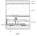
図6に、ボトムゲート型薄膜トランジスタを用いた液晶表示装置の一態様の断面模式図を示し、図7、図8にこの液晶表示装置の製造工程を示す。
【0004】
この製造工程では、まず、透明ガラス基板1の上に、Cr、Al、Mo、Ta等の金属を用いてゲート電極2を200nm厚程度形成する。また、同様にCs電極3を形成する(図7(a))。
【0005】
ゲート電極2上には、ゲート絶縁膜6として、例えば、窒化シリコン膜4を50nm、酸化シリコン膜5を150nm積層する。ゲート絶縁膜6の積層後、引き続きアモルファスシリコン膜を50nm積層する。その後、赤外線ランプを用いた熱アニールやレーザーアニール等の手法でアモルファスシリコン膜を結晶化し、ポリシリコン膜7とする(図7(b))。
【0006】
次に、酸化シリコンによる保護絶縁膜8を200nm成膜し(図7(c))、保護絶縁膜8上にレジストを形成し、ゲート電極2をマスクとして裏面から露光することにより、ゲート電極2と自己整合したチャンネル形成部分上にレジストをパターニングし、このレジストをマスクとして保護絶縁膜8をエッチング除去し、ゲート電極2と自己整合したチャンネル形成部分に保護絶縁膜8を残す(図7(d))。このエッチングには、通常、フッ素酸系ウェットエッチングやフッ素系ドライエッチングが用いられる。
【0007】
次に、酸化シリコンによる保護絶縁膜8をマスクとして、燐、砒素等をイオン注入してLDD(lightly doped drain)領域9を形成し(図7(e))、次いで、Nチャンネルソース・ドレイン注入用レジストマスク(SD注入マスク)11をレジスト等により形成し、次いで、ソース・ドレイン領域(SD領域)、及びポリシリコン膜7とゲート電極2により形成する補助容量領域のポリシリコン膜7上の保護絶縁膜8を、フッ素酸系ウェットエッチングやフッ素系ドライエッチングにより除去する(図7(f))。その後、高濃度の燐、砒素等の注入によりNチャンネルソース・ドレイン領域(SD領域)10を形成する。さらに、注入した燐等のドーパントを活性化するために、熱アニールやレーザーアニールを行い、ドーパントの非注入部分のポリシリコン膜7を能動層とし、TFT100を得る(図7(g))。
【0008】
次に、この基板1のTFT100の形成部分にレジストを形成し、不要部分の保護絶縁膜及びポリシリコン膜7をパターニングする(図8(h))。この場合も、保護絶縁膜のエッチングには、通常、フッ素酸系ウェットエッチングやフッ素系ドライエッチングが用いられる。また、ポリシリコン膜7のエッチングには、F系又はCl系ドライエッチングが多く用いられる。
【0009】
次に、層間絶縁膜13を形成するため、窒化シリコン膜14(300nm)、酸化シリコン膜15(200nm)を連続形成する(図8(i))。
【0010】
この層間絶縁膜13及びゲート絶縁膜6は、ポリシリコン膜7上のコンタクト形成部分、ゲート電極2上のコンタクト形成部分(図示せず)においてエッチング除去し、コンタクトホール16を形成する(図8(j))。そして、コンタクトホール16にAl等の金属を埋め込むことにより、ソース電極17、ドレイン電極18を形成する(図8(k))。
【0011】
次に、液晶表示パネルの透明電極とコンタクトを形成する部分やパッド形成部分等を除いた領域に、有機平坦化膜、窒化シリコン平坦化膜等の平坦化膜19を形成し、その後、画素部分を覆うようにITO等の透明電極20を形成し、透明電極20上には、配向膜21を形成する。こうして、液晶表示装置用のTFT基板201が形成される(図8(l))。
【0012】
図6の液晶表示装置200は、以上のようにして形成されたTFT基板201と、対向電極202を備えた対向基板203と、両者の間に保持される液晶204とからパネル構造を形成することにより得られる。
【0013】
【発明が解決しようとする課題】
図6〜図8に示した従来の液晶表示装置に使用されているTFT100の構造では、補助容量を、燐等を高濃度にドープしたポリシリコン膜7とCs電極3(ゲート電極2と同一層)により構成しているが、その形状を形成するためにポリシリコン膜7上の保護絶縁膜8を2回にわたってエッチング除去しなくてはならず(図7(d)、(f))、このために工程が複雑になり、生産性向上の妨げとなっている。
【0014】
また、1回目に保護絶縁膜8をエッチング除去した領域は(図7(d))、保護絶縁膜8の2回目のエッチング除去を行う工程において、エッチング初期よりポリシリコン膜7が露出している(図7(f))。一方、この時点でポリシリコン膜7は、燐、砒素等がイオン注入されることによりNチャンネル化したLDD領域9に形成されているので、アルカリ系のレジスト剥離液やフッ素酸系エッチング液に浸食され、ピンホール等が生じやすくなっている。このため、この部分のポリシリコン膜7や、その下部のゲート絶縁膜6(特に酸化シリコン膜5)は、フッ素酸系エッチング液にエッチングされ、ポリシリコン膜7とCs電極3(又はゲート電極2)との間でゲート絶縁膜6の耐圧が低下するという問題があった。
【0015】
本発明は以上のような従来技術の問題点を解決しようとするものであり、ボトムゲート型TFTにおいて、製造工程を削減して生産性を向上させ、また、ゲート絶縁膜の耐圧不良を防止し、製品の歩留まりを向上させることを目的としている。
【0016】
【課題を解決するための手段】
本発明者らは、従来のボトムゲート型TFTの製造工程において、膜厚200nm程度に形成していた保護絶縁膜8を100nm以下とし、以降のLDD領域9、あるいはソース・ドレイン領域10の形成時に保護絶縁膜8を通してドーパントを注入することにより、保護絶縁膜8のエッチング工程を削減できること、またゲート絶縁膜6の耐圧不良の問題も解消できることを見出した。さらに、このようなTFTの構造あるいはその製造方法は、TFTで駆動される液晶表示装置や有機EL装置にも適用できることを見出した。
【0017】
即ち、本発明は、透明基板と透明基板上に設けられている厚さ10〜400nmの金属ゲート電極、及び、Cs電極と、ゲート電極及びCs電極を覆って透明基板上の全面に形成された、ゲート絶縁膜とを備える。そして、ゲート絶縁膜上に形成されたCs電極上の一部が除去されたパターンを有する10〜100nmの厚さの能動層と、能動層上に形成されたCs電極上の一部が除去されたパターンを有する厚さ5〜100nmの酸化シリコン膜からなる保護絶縁膜と、チャネル領域を除く金属ゲート電極上の能動層に設けられたLDD領域を備える。さらに、能動層のチャネル領域及びLDD領域を除く領域において、チャネル領域及びLDD領域と同一層に形成されているソース・ドレイン領域を備え、能動層が、保護絶縁膜の形成後の熱アニール又はレーザアニールによって結晶化されたアモルファスシリコン膜から形成されている薄膜トランジスタを提供する。
【0018】
また、本発明は上述の薄膜トランジスタの製造方法として、透明基板上に金属ゲート電極、及び、Cs電極を10〜400nmの厚さで形成する。そして、ゲート電極及びCs電極を覆って、透明基板上の全面に窒化シリコン膜を10〜100nmの厚さで形成し、窒化シリコン膜上に酸化シリコン膜を50〜200nmの厚さで形成して、ゲート絶縁膜を形成する。さらに、ゲート絶縁膜上にアモルファスシリコン膜を10〜100nmの厚さで形成する工程と、アモルファスシリコン膜を熱アニール又はレーザアニールにより結晶化して能動層を形成する。次に、能動層上に酸化シリコン膜を5〜100nmの厚さで形成して保護絶縁膜を形成し、Cs電極上の能動層及び保護絶縁膜の一部を除去し、保護絶縁膜上にLDD用マスクを形成し、チャネル領域を除く金属ゲート電極上の能動層に、不純物を注入してLDD領域を形成する。保護絶縁膜上にソース・ドレイン用マスクを形成し、能動層のチャネル領域及びLDD領域を除く領域において、チャネル領域及びLDD領域と同一層に不純物を注入してソース・ドレイン領域を形成し、熱アニール又はレーザアニールにより注入した不純物を活性化する。
【0019】
さらに本発明は、上述の本発明のボトムゲート型薄膜トランジスタ上に形成された厚さ50〜500nmの窒化シリコン膜、及び、窒化シリコン膜上に形成された厚さ50〜500nmの酸化シリコン膜からなる層間絶縁膜を備える。また、ソース・ドレイン領域上の層間絶縁膜及び保護絶縁膜に形成されたコンタクトホールと、コンタクトホール内に埋め込まれた金属からなるソース電極及びドレイン電極と、ソース電極及びドレイン電極を覆って、層間絶縁膜上に設けられた平坦化膜と、平坦化膜上に設けられた、画素部分を覆う透明電極と、透明電極上に設けられた配向膜と、ボトムゲート型薄膜トランジスタ上に設けられた対向電極を備える対向基板と、ボトムゲート型薄膜トランジスタと対向基板とに挟持された液晶とを備える液晶表示装置を提供し、また、上述の本発明のボトムゲート型薄膜トランジスタの製造方法においてボトムゲート型薄膜トランジスタの不要部分の保護絶縁膜と能動層を除去する工程と、ボトムゲート型薄膜トランジスタ上に、窒化シリコン膜を50〜500nmの厚さで形成し、窒化シリコン膜上に酸化シリコン膜を50〜500nmの厚さで形成して、層間絶縁膜を形成する工程と、ソース・ドレイン領域上の層間絶縁膜及び保護絶縁膜を除去してコンタクトホールを形成する工程と、コンタクトホールに金属を埋め込んでソース電極及びドレイン電極を形成する工程と、ソース電極及びドレイン電極を覆って、層間絶縁膜上に平坦化膜を形成する工程と、平坦化膜上に、画素部分を覆う透明電極を形成する工程と、透明電極上に配向膜を形成する工程と、ボトムゲート型薄膜トランジスタ上に、対向電極を備える対向基板を設ける工程と、ボトムゲート型薄膜トランジスタと対向基板とに液晶を挟持させる工程と、を有する液晶表示装置の製造方法を提供する。
【0020】
また、本発明は、上述の本発明のボトムゲート型薄膜トランジスタ上に形成された厚さ50〜500nmの窒化シリコン膜、及び、窒化シリコン膜上に形成された厚さ50〜500nmの酸化シリコン膜からなる層間絶縁膜と、ソース・ドレイン領域上の層間絶縁膜及び保護絶縁膜に形成されたコンタクトホールと、コンタクトホール内に埋め込まれた金属からなるソース電極及びドレイン電極と、ソース電極及びドレイン電極を覆って、層間絶縁膜上に設けられた平坦化膜と、平坦化膜に設けられたコンタクトホールと、平坦化膜上に設けられ、コンタクトホールを介してボトムゲート型薄膜トランジスタのソース電極に導通する陰極層と、陰極層上に、電子輸送層を形成する工程と、電子輸送層上に設けられた発光層と、発光層上に設けられた正孔輸送層と、正孔輸送層上に設けられた陽極層とを備える有機EL装置を提供し、また、上述の本発明のボトムゲート型薄膜トランジスタの製造方法においてボトムゲート型薄膜トランジスタの不要部分の保護絶縁膜と能動層を除去する工程と、ボトムゲート型薄膜トランジスタ上に、窒化シリコン膜を50〜500nmの厚さで形成し、窒化シリコン膜上に酸化シリコン膜を50〜500nmの厚さで形成して、層間絶縁膜を形成する工程と、ソース・ドレイン領域上の層間絶縁膜及び保護絶縁膜を除去してコンタクトホールを形成する工程と、コンタクトホールに金属を埋め込んでソース電極及びドレイン電極を形成する工程と、ソース電極及びドレイン電極を覆って、層間絶縁膜上に平坦化膜を形成する工程と、平坦化膜に、コンタクトホールを形成する工程と、平坦化膜上に、コンタクトホールを介してボトムゲート型薄膜トランジスタのソース電極に導通する陰極層を形成する工程と、陰極層上に、電子輸送層を形成する工程と、電子輸送層上に、発光層を形成する工程と、発光層上に、正孔輸送層を形成する工程と、正孔輸送層上に、陽極層を形成する工程と、を有する有機EL装置の製造方法を提供する。
【0021】
【発明の実施の形態】
以下、本発明を図面を参照しつつ詳細に説明する。なお、各図中、同一符号は同一又は同等の構成要素を表している。
【0022】
図1は、本発明のボトムゲート型薄膜トランジスタを用いた液晶表示装置の一態様の断面模式図であり、図2、図3は、その製造工程図である。
【0023】
本態様の製造方法において、(1)基板上にゲート電極を形成する工程、及び(2)ゲート電極上にゲート絶縁膜を形成する工程は、前述の従来の製造方法と同様とすることができる。即ち、まず、工程(1)では、透明ガラス基板1の上に、Cr、Al、Mo、Ta等の金属を用いてゲート電極2を10〜400nm形成する。ゲート電極2は必要に応じて酸化処理し、該ゲート電極2上に、ゲート酸化膜の一部として機能する絶縁層を形成してもよい。また、同様にしてCs電極3を形成する(図2(A))。
【0024】
工程(2)では、ゲート電極2上に、ゲート絶縁膜6として、例えば、窒化シリコン膜4をプラズマCVD法により10〜100nm積層し、酸化シリコン膜5をプラズマCVD法により50〜200nm積層する(図2(B))。窒化シリコン膜4、酸化シリコン膜5の成膜は、ECR−CVD法や熱CVD法等によってもよい。
【0025】
本態様の製造方法において、本発明の製造方法における工程(3)、即ち、「ゲート絶縁膜上に能動層前駆体膜及び保護絶縁膜が積層されており、該保護絶縁膜が膜厚100nm以下である積層体を形成する工程」としては、ゲート絶縁膜6の積層後、まず、アモルファスシリコン膜をプラズマCVD法により10〜100nm積層し、そのアモルファスシリコン膜を、赤外線ランプを用いた熱アニールやレーザーアニール等の手法で結晶化し、ポリシリコン膜7とする(図2(C))。このポリシリコン膜7が、能動層となる。ポリシリコン膜7の形成方法としては、熱CVD法等により直接的にポリシリコン膜7を成膜してもよい。
【0026】
続いて、熱CVD法、プラズマCVD法等により酸化シリコンからなる保護絶縁膜8を100nm以下成膜する(図2(C))。
【0027】
本発明においては、このように保護絶縁膜8を100nm以下形成し、以降のLDD領域、あるいはソース・ドレイン領域の形成工程において、保護絶縁膜8をエッチングすることなく、保護絶縁膜8を通して燐、砒素等のドーパントを注入することを特徴としている。これにより、従来法の保護絶縁膜8のエッチング工程(図7(d)、(f))を削減できるので、生産性を向上させることができる。また、ポリシリコン膜7が不要にエッチングされないので、ゲート絶縁膜6の耐圧不良を防止でき、また、ポリシリコン膜7の点欠陥や線欠陥を著しく減少させ、製品の歩留まりを向上させることができる。
【0028】
ここで、保護絶縁膜8の膜厚は、この保護絶縁膜8を通して燐、砒素等のドーパントを注入する際の注入装置の加速電圧の限界の点から、100nm以下とするが、加速電圧の低い注入装置を使用して製造コストを下げる点からは、保護絶縁膜8の膜厚は50nm以下とすることが好ましい。一方、保護絶縁膜8を形成しないと、LDD領域の形成工程において、能動層となるポリシリコン膜7にLDD領域形成用レジストマスク(LDD注入マスク)が直接接触し、また後のソース・ドレイン領域の形成工程においてもNチャンネルSD注入マスクやPチャンネルSD注入マスクが直接接触することとなるのでポリシリコン膜7の汚染の問題が発生する。したがって、保護絶縁膜8の膜厚としては、5nm以上とすることが好ましい。
【0029】
本態様の製造方法において、本発明の製造方法における工程(4)、即ち、「保護絶縁膜を通して能動層前駆体膜のLDD領域又はソース・ドレイン領域にドーパントを注入する工程」としては、まず、保護絶縁膜8上にLDD注入マスク22を形成し、燐、砒素等を注入してLDD領域9を形成し(図2(D))、次に、Nチャンネルソース・ドレイン領域(SD領域)10を形成するために、NチャンネルSD注入マスク11を形成し、高濃度の燐、砒素等を注入する。その際、ポリシリコン膜7とゲート電極2により形成する補助容量領域のポリシリコン膜7にも注入を行うため、レジストマスクは補助容量領域には形成しない。なお、ここでC−MOS回路等を形成する場合には、Pチャンネルソース・ドレイン領域を形成するため、再度、レジスト等によりマスクを形成し、硼素等を注入する。
【0030】
その後、本発明の工程(5)として、注入した燐等のドーパントを活性化するために、熱アニールやレーザーアニールを行う。こうして、本発明のTFT100Aを得る(図2(E))。
【0031】
このTFT100Aを駆動素子とする液晶表示装置を製造するためには、次に、TFT100Aの形成部分にレジストを形成し、不要部分の保護絶縁膜8及びポリシリコン膜7をパターニングする(図2(F))。この場合も、保護絶縁膜8のエッチングには、通常、フッ素酸系ウェットエッチングやフッ素系ドライエッチングが用いられる。また、ポリシリコン膜7のエッチングには、F系又はCl系ドライエッチングが多く用いられる。
【0032】
その後、層間絶縁膜13の形成、ソース電極17及びドレイン電極18の形成、平坦化膜19の形成、透明電極20の形成、透明電極20上への配向膜21の形成を行うが、これらは、前述の従来法と同様とすることができる。即ち、層間絶縁膜13を形成するため、窒化シリコン膜14(50〜500nm)、酸化シリコン膜15(50〜500nm)を連続形成し(図3(G))、次に、層間絶縁膜13及びゲート絶縁膜6をエッチング除去してコンタクトホールを形成16し(図3(H))、コンタクトホール16にAl等の金属を埋め込むことによりソース電極17、ドレイン電極18を形成する(図3(I))。そして、液晶表示パネルの透明電極とのコンタクトを形成する部分やパッド形成部分等を除いた領域に、有機平坦化膜、窒化シリコン平坦化膜等の平坦化膜19を形成し、その後、画素部分を覆うようにITO等の透明電極20を形成し、透明電極20上に配向膜21を形成する。こうして、本発明のTFT100Aを駆動素子とする液晶表示装置用のTFT基板201Aを得る(図3(J))。
【0033】
図1の液晶表示装置200Aは、上述のTFT基板201Aと、公知の対向電極202を備えた対向基板203とを組み合わせ、常法により双方の基板の間に液晶204を挟持させることにより製造することができる。
【0034】
以上、TFTを用いた液晶表示装置200Aを例として、本発明の一態様のTFT及びその製造方法を説明したが、本発明のTFTあるいはその製造方法は、能動層前駆体膜上の保護絶縁膜8を100nm以下とし、この保護絶縁膜8を通してドーパントを注入し、LDD領域、あるいはソース・ドレイン領域を形成する限り、種々の態様をとることができる。
【0035】
例えば、上述の本発明のTFT 100Aでは、ドーパントを注入する能動層前駆体膜をポリシリコン膜7としたが、本発明において、能動層前駆体膜はこれに限らない。例えば、アモルファスシリコン膜、シリコンゲルマニウム膜、シリコンカーバイト膜等を能動層前駆体膜として用いてもよい。プロセスとの整合性の点からは、ポリシリコン膜を使用することが好ましい。
【0036】
また、上述の本発明のTFT 100Aでは、工程(3)において、ゲート絶縁膜6上にアモルファスシリコン膜を積層し、そのアモルファスシリコン膜を結晶化してポリシリコン膜7とし、そのポリシリコン膜7上に保護絶縁膜8を成膜しているが、アモルファスシリコン膜をCVD法等で形成後、そのアモルファスシリコン膜を結晶化することなく、チャンバーの真空度を破ることなく連続的にCVD法で保護絶縁膜8を成膜し、その後アモルファスシリコン膜を結晶化してポリシリコン膜7を形成してもよい。これにより、ポリシリコン膜7のいっそうの汚染防止を図ることができる。
【0037】
さらに、上述の本発明のTFT 100Aでは、工程(3)において、酸化シリコンからなる保護絶縁膜8をプラズマCVD法等により成膜しているが、ポリシリコン膜7とするアモルファスシリコン膜の表面酸化により保護絶縁膜8を形成してもよい。表面酸化の手法としては、例えば、400℃程度の熱水蒸気やオゾンガスに晒したり、あるいは酸素を含む雰囲気で紫外線を照射する。この方法によると、5〜20nmのシリコン酸化膜を膜厚制御よく形成できるので、レーザーアニール等によってアモルファスシリコン膜を結晶化し、ポリシリコン膜7を形成する際のポリシリコン膜の膜厚及び結晶化の制御性が向上する。
【0038】
また、本発明では、保護絶縁膜8を通してドーパントを注入し、LDD領域、あるいはソース・ドレイン領域を形成するので保護絶縁膜8に欠陥が発生する。特に、LDD領域では注入量が少ないため、保護絶縁膜8の上部の欠陥により抵抗変化が生じる。さらに、プロセスの途中では、固化したレジストの剥離のためにアッシング工程等を行うが、これによってもチャンネル又はLDD領域上部の保護絶縁膜8に欠陥が生じる。これに対しては、欠陥回復のための処理を行うことが好ましい。より具体的には、工程(4)のソース・ドレイン領域10の形成後、又は層間絶縁膜13の形成後に200〜650℃程度の熱エネルギー照射、RTA、レーザー照射等を行うことが好ましい。特に、この欠陥回復のための処理は、工程(4)において注入したドーパントの活性化工程と兼ねるか、あるいは窒化シリコン膜14の形成後に行うポリシリコン膜7の水素化工程と兼ねると、工程数が増加しないので好ましい。ドーパントの活性化工程で、欠陥回復が併せて行われるようにするための処理条件としてはRTA法等により瞬間的に600℃程度とすることが好ましい。
【0039】
本発明のTFTあるいはその製造方法は、液晶表示装置の他に、TFTを駆動素子とする有機EL装置あるいはその製造方法にも適用することができる。
【0040】
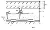
例えば、図4の有機EL装置300は、前述の製造方法に準じてTFT基板を作製し、公知の有機EL装置の製造方法(特開平11−251069号公報、特開平10−189252号公報等)にしたがい、次のように製造することができる。まず、透明ガラス基板1上に、ゲート電極2、ゲート絶縁膜6、ポリシリコン膜7からなる能動層、及び膜厚100nm以下の保護絶縁膜8が順次積層したTFT100Aを形成する。次に、TFT100A上に層間絶縁膜13を形成し、さらにソース電極17及びドレイン電極18を形成し、平坦化膜19を形成し、平坦化膜19にコンタクトホール23を開孔する。平坦化膜19上に、有機EL素子30の陰極層31を形成し、コンタクトホール23を介してTFT100Aのソース電極17と陰極層31を導通させる。陰極層31上には、電子輸送層32、発光層33、正孔輸送層34を順次形成し、さらに正孔輸送層34上に陽極層35を形成する。こうして、陽極層35から注入された正孔と陰極層31から注入された電子とが発光層33の内部で再結合し、発光が生じる有機EL素子30であって、その発光が本発明のTFTで駆動される有機EL装置300を作製することができる。なお、この有機EL装置300では、光を陽極層35側から取り出すことができる。
【0041】
ここで、有機EL素子30それ自体の層構成や各層の形成素材等については特に制限はなく、TFT100Aと有機EL素子30との間の平坦化膜19の形成素材や形成方法についても特に制限はない。
【0042】
例えば、平坦化膜19は、酸化シリコン膜、窒化シリコン膜、シリコン窒化酸化膜、シリケートガラス膜、SOG膜、ポリイミド系、アクリル系等の合成樹脂膜等から形成することができる。
【0043】
陰極層31は、マグネシウム・インジウム合金、アルミニウム・リチウム合金等から形成できる。電子輸送層32は、Bebq2(10−ベンゾ[h]キノリノール−ベリリウム錯体)等から形成でき、発光層33は、キナクリドン(Quinacridone)誘導体を含むBebq2、8−キノリノールアルミニウム錯体等から形成でき、正孔輸送層34は、TPD(4,4',4''-tris-(methylphenylphenylamino)triphenylamine)、MTDATA(4,4'-bis(3-methylphenylphenylamino)biphenyl)、α−NPD(α-naphtylphenyldiamine)等から形成でき、陽極層35はPt、Rh、Pd等から形成することができる。これらの各層は、蒸着法等により形成することができる。また、陽極層35は、スパッタ法によりITO等から形成してもよい。
【0044】
TFTで駆動される有機EL装置としては、図5に示すように、TFT100A上の有機EL素子30の層構成を逆転させ、平坦化膜19上に、陽極層35、正孔輸送層34、発光層33、電子輸送層32、及び陰極層31を順次積層させてもよい。この有機EL装置では、光を基板1側から取り出すことができる。
【0045】
この他、本発明の有機EL装置は、本発明のTFTを使用する限り、種々の態様を包含する。
【0046】
【発明の効果】
本発明によれば、ボトムゲート型TFTにおいて、能動層となるポリシリコン膜上の保護絶縁膜の膜厚を100nm以下とし、保護絶縁膜を通してLDD領域あるいはソース・ドレイン領域を形成するので、LDD領域あるいはソース・ドレイン領域の形成のために保護絶縁膜をエッチングする工程が不要となる。したがって、製造工程を削減し、TFTの生産性を向上させることが可能となる。また、ゲート絶縁膜の耐圧不良を防止することができ、また、能動層の点欠陥や線欠陥が著しく減少し、製品の歩留まりが向上する。
【図面の簡単な説明】
【図1】 本発明のTFTを用いた液晶表示装置の断面模式図である。
【図2】 本発明のTFTを用いた液晶表示装置の製造工程図である。
【図3】 本発明のTFTを用いた液晶表示装置の製造工程図である。
【図4】 本発明のTFTを用いた有機EL装置の断面模式図である。
【図5】 本発明のTFTを用いた有機EL装置の断面模式図である。
【図6】 従来のTFTを用いた液晶表示装置の断面模式図である。
【図7】 従来のTFTを用いた液晶表示装置の製造工程図である。
【図8】 従来のTFTを用いた液晶表示装置の製造工程図である。
【符号の説明】
1…透明ガラス基板、 2…ゲート電極、 3…Cs電極、 4…窒化シリコン膜、 5…酸化シリコン膜、 6…ゲート絶縁膜、 7…ポリシリコン膜、 8…保護絶縁膜、 9…LDD領域、 10…ソース・ドレイン領域、 11…SD注入マスク、 13…層間絶縁膜、 14…窒化シリコン膜、 15…酸化シリコン膜、 17…ソース電極、 18…ドレイン電極、 20…透明電極、21…配向膜、 30…有機EL素子、 31…陰極層、 32…電子輸送層、 33…発光層、 34…正孔輸送層、 35…陽極層、 100A…TFT、 200A…液晶表示装置、 201A…TFT基板、 202…対向電極、 203…対向基板、 204…液晶、 300…有機EL装置[0001]
BACKGROUND OF THE INVENTION
The present invention relates to a bottom-gate thin film transistor and a method for manufacturing the same, and a liquid crystal display element and an organic EL device using the bottom-gate thin film transistor.
[0002]
[Prior art]
Thin film transistors (TFTs) are used as switching elements in active matrix liquid crystal display devices, active matrix organic EL display devices, and the like. Thin film transistors are roughly classified into bottom gate type and top gate type because of their structure. Of these, bottom gate type thin film transistors are provided with a gate electrode under the active layer, and are more reliable than top gate type thin film transistors. ing. Regarding the structure of the bottom gate type thin film transistor, for example, “'99 latest liquid crystal process technology” (Press Journal 1998, pp53-59), “Flat Panel Display 1999” (Nikkei BP, 1998, pp132- 139) and JP-A-8-279618.
[0003]
FIG. 6 shows a schematic cross-sectional view of one embodiment of a liquid crystal display device using a bottom-gate thin film transistor, and FIGS. 7 and 8 show manufacturing steps of the liquid crystal display device.
[0004]
In this manufacturing process, first, the
[0005]
On the
[0006]
Next, a protective
[0007]
Next, using the protective
[0008]
Next, a resist is formed on the portion of the
[0009]
Next, in order to form the
[0010]
The
[0011]
Next, a
[0012]
The liquid
[0013]
[Problems to be solved by the invention]
In the structure of the
[0014]
In the region where the protective
[0015]
The present invention is intended to solve the above-mentioned problems of the prior art, and in the bottom gate type TFT, it is possible to improve the productivity by reducing the manufacturing process and prevent the breakdown voltage of the gate insulating film. The goal is to improve product yield.
[0016]
[Means for Solving the Problems]
In the manufacturing process of the conventional bottom gate type TFT, the inventors set the protective
[0017]
That is, the present invention is formed on the entire surface of the transparent substrate so as to cover the transparent substrate, the metal gate electrode having a thickness of 10 to 400 nm provided on the transparent substrate, the Cs electrode, and the gate electrode and the Cs electrode. And a gate insulating film. And formed on the gate insulating filmIt has a pattern in which part of the Cs electrode is removed. 10-100 nm thick active layer and formed on the active layerIt has a pattern in which part of the Cs electrode is removed. A protective insulating film made of a silicon oxide film having a thickness of 5 to 100 nm and an LDD region provided in an active layer on the metal gate electrode excluding the channel region are provided. further,Active layer Excluding channel region and LDD regionIn the region, it is formed in the same layer as the channel region and the LDD region There is provided a thin film transistor including a source / drain region and an active layer formed of an amorphous silicon film crystallized by thermal annealing or laser annealing after the formation of a protective insulating film.
[0018]
Further, according to the present invention, as a method of manufacturing the above-described thin film transistor, a metal gate electrode and a Cs electrode are formed on a transparent substrate with a thickness of 10 to 400 nm. Then, a silicon nitride film is formed to a thickness of 10 to 100 nm on the entire surface of the transparent substrate, covering the gate electrode and the Cs electrode, and a silicon oxide film is formed to a thickness of 50 to 200 nm on the silicon nitride film. Then, a gate insulating film is formed. Furthermore, an amorphous silicon film is formed on the gate insulating film with a thickness of 10 to 100 nm, and the amorphous silicon film is crystallized by thermal annealing or laser annealing to form an active layer. Next, a silicon oxide film is formed on the active layer with a thickness of 5 to 100 nm to form a protective insulating film,Removing part of the active layer and protective insulating film on the Cs electrode; An LDD mask is formed on the protective insulating film, and an LDD region is formed by implanting impurities into the active layer on the metal gate electrode excluding the channel region. A source / drain mask is formed on the protective insulating film,Active layer Excluding channel region and LDD regionIn the same layer as the channel region and LDD region Impurities are implanted to form source / drain regions, and the implanted impurities are activated by thermal annealing or laser annealing.
[0019]
Furthermore, the present invention provides the above-described bottom gate type thin film transistor of the present invention.An interlayer insulating film is formed of a silicon nitride film having a thickness of 50 to 500 nm formed thereon and a silicon oxide film having a thickness of 50 to 500 nm formed on the silicon nitride film. Further, contact holes formed in the interlayer insulating film and the protective insulating film on the source / drain regions, a source electrode and a drain electrode made of metal embedded in the contact holes, and covering the source electrode and the drain electrode, A planarization film provided on the insulating film, a transparent electrode provided on the planarization film covering the pixel portion, an alignment film provided on the transparent electrode, and a counter provided on the bottom-gate thin film transistor A counter substrate including electrodes, and a liquid crystal sandwiched between the bottom gate thin film transistor and the counter substrate. A liquid crystal display device is provided, and the above-described bottom gate thin film transistor manufacturing method of the present invention is provided.A step of removing a protective insulating film and an active layer of unnecessary portions of the bottom gate type thin film transistor, a silicon nitride film having a thickness of 50 to 500 nm is formed on the bottom gate type thin film transistor, and a silicon oxide film is formed on the silicon nitride film. A step of forming an interlayer insulating film with a thickness of 50 to 500 nm, a step of removing the interlayer insulating film and the protective insulating film on the source / drain regions to form a contact hole, and a metal in the contact hole A step of embedding and forming a source electrode and a drain electrode; a step of covering the source electrode and the drain electrode; forming a planarization film on the interlayer insulating film; and forming a transparent electrode covering the pixel portion on the planarization film A step of forming an alignment film on the transparent electrode, and a step of providing a counter substrate having a counter electrode on the bottom-gate thin film transistor , And a step for sandwiching a liquid crystal in a bottom gate type thin film transistor and the opposite substrate A method for manufacturing a liquid crystal display device is provided.
[0020]
The present invention also provides the above-described bottom-gate thin film transistor of the present invention.An interlayer insulating film formed on the silicon nitride film having a thickness of 50 to 500 nm formed thereon, a silicon oxide film having a thickness of 50 to 500 nm formed on the silicon nitride film, and an interlayer insulating film on the source / drain regions And a contact hole formed in the protective insulating film, a source electrode and a drain electrode made of metal embedded in the contact hole, and a planarizing film provided on the interlayer insulating film so as to cover the source electrode and the drain electrode A contact hole provided in the planarization film, a cathode layer provided on the planarization film and conducting to the source electrode of the bottom gate thin film transistor through the contact hole, and an electron transport layer formed on the cathode layer A step, a light emitting layer provided on the electron transport layer, a hole transport layer provided on the light emitting layer, and an anode layer provided on the hole transport layer An organic EL device is provided, and the above-described bottom-gate thin film transistor manufacturing method of the present invention is provided.A step of removing a protective insulating film and an active layer of unnecessary portions of the bottom gate type thin film transistor, a silicon nitride film having a thickness of 50 to 500 nm is formed on the bottom gate type thin film transistor, and a silicon oxide film is formed on the silicon nitride film. A step of forming an interlayer insulating film with a thickness of 50 to 500 nm, a step of removing the interlayer insulating film and the protective insulating film on the source / drain regions to form a contact hole, and a metal in the contact hole A step of burying and forming a source electrode and a drain electrode; a step of covering the source electrode and the drain electrode; forming a planarization film on the interlayer insulating film; forming a contact hole in the planarization film; A step of forming a cathode layer on the oxide film, which is electrically connected to the source electrode of the bottom-gate thin film transistor through the contact hole; A step of forming an electron transport layer on the layer, a step of forming a light emitting layer on the electron transport layer, a step of forming a hole transport layer on the light emitting layer, and an anode on the hole transport layer. Forming a layer A method for manufacturing an organic EL device is provided.
[0021]
DETAILED DESCRIPTION OF THE INVENTION
Hereinafter, the present invention will be described in detail with reference to the drawings. In each figure, the same numerals indicate the same or equivalent components.
[0022]
FIG. 1 is a schematic cross-sectional view of an embodiment of a liquid crystal display device using a bottom-gate thin film transistor of the present invention, and FIGS. 2 and 3 are manufacturing process diagrams thereof.
[0023]
In the manufacturing method of this aspect, (1) the step of forming a gate electrode on the substrate and (2) the step of forming a gate insulating film on the gate electrode can be the same as the above-described conventional manufacturing method. . That is, first, in the step (1), the
[0024]
In step (2), as the
[0025]
In the manufacturing method of this aspect, step (3) in the manufacturing method of the present invention, that is, “an active layer precursor film and a protective insulating film are laminated on a gate insulating film, and the protective insulating film has a thickness of 100 nm or less. As the step of forming a laminated body that is, after the
[0026]
Subsequently, a protective
[0027]
In the present invention, the protective
[0028]
Here, the thickness of the protective
[0029]
In the manufacturing method of this aspect, as the step (4) in the manufacturing method of the present invention, that is, “the step of implanting a dopant into the LDD region or the source / drain region of the active layer precursor film through the protective insulating film” An
[0030]
Thereafter, as step (5) of the present invention, thermal annealing or laser annealing is performed to activate the implanted dopant such as phosphorus. Thus, the
[0031]
In order to manufacture a liquid crystal display device using the
[0032]
Thereafter, the
[0033]
The liquid
[0034]
As described above, the TFT of one embodiment of the present invention and the manufacturing method thereof have been described using the liquid
[0035]
For example, in the
[0036]
Further, in the
[0037]
Further, in the
[0038]
In the present invention, since the dopant is implanted through the protective
[0039]
The TFT of the present invention or a manufacturing method thereof can be applied to an organic EL device using a TFT as a driving element or a manufacturing method thereof in addition to a liquid crystal display device.
[0040]
For example, in the
[0041]
Here, there are no particular restrictions on the layer configuration of the
[0042]
For example, the
[0043]
The
[0044]
As an organic EL device driven by a TFT, as shown in FIG. 5, the layer configuration of the
[0045]
In addition, the organic EL device of the present invention includes various modes as long as the TFT of the present invention is used.
[0046]
【The invention's effect】
According to the present invention, in the bottom gate TFT, the thickness of the protective insulating film on the polysilicon film serving as the active layer is 100 nm or less, and the LDD region or the source / drain region is formed through the protective insulating film. Alternatively, the step of etching the protective insulating film is not required for forming the source / drain regions. Therefore, it is possible to reduce the manufacturing process and improve the productivity of the TFT. In addition, a breakdown voltage failure of the gate insulating film can be prevented, and point defects and line defects in the active layer are remarkably reduced, thereby improving product yield.
[Brief description of the drawings]
FIG. 1 is a schematic cross-sectional view of a liquid crystal display device using a TFT of the present invention.
FIG. 2 is a manufacturing process diagram of a liquid crystal display device using the TFT of the present invention.
FIG. 3 is a manufacturing process diagram of a liquid crystal display device using the TFT of the present invention.
FIG. 4 is a schematic cross-sectional view of an organic EL device using the TFT of the present invention.
FIG. 5 is a schematic cross-sectional view of an organic EL device using the TFT of the present invention.
FIG. 6 is a schematic cross-sectional view of a liquid crystal display device using a conventional TFT.
FIG. 7 is a manufacturing process diagram of a liquid crystal display device using a conventional TFT.
FIG. 8 is a manufacturing process diagram of a liquid crystal display device using a conventional TFT.
[Explanation of symbols]
DESCRIPTION OF
Claims (6)
Translated fromJapanese前記透明基板上に設けられている厚さ10〜400nmの金属ゲート電極、及び、Cs電極と、
前記ゲート電極及び前記Cs電極を覆って前記透明基板上の全面に形成された厚さ10〜100nmの窒化シリコン膜、及び、前記窒化シリコン膜上に形成された厚さ50〜200nm酸化シリコン膜からなるゲート絶縁膜と、
前記ゲート絶縁膜上に形成され、前記Cs電極上の一部が除去されたパターンを有する、10〜100nmの厚さの能動層と、
前記能動層上に形成され、前記Cs電極上の一部が除去されたパターンを有する、厚さ5〜100nmの酸化シリコン膜からなる保護絶縁膜と、
チャネル領域を除く前記金属ゲート電極上の前記能動層に設けられたLDD領域と、
前記能動層の前記チャネル領域及び前記LDD領域を除く領域において、前記チャネル領域及び前記LDD領域と同一層に形成されているソース・ドレイン領域と、を備え、
前記能動層が、前記保護絶縁膜の形成後の熱アニール又はレーザアニールによって結晶化されたアモルファスシリコン膜から形成されている
薄膜トランジスタ。A transparent substrate, a metal gate electrode having a thickness of 10 to 400 nm provided on the transparent substrate, and a Cs electrode;
A silicon nitride film having a thickness of 10 to 100 nm formed on the entire surface of the transparent substrate so as to cover the gate electrode and the Cs electrode, and a silicon oxide film having a thickness of 50 to 200 nm formed on the silicon nitride film. A gate insulating film,
An active layer having a thickness of 10 to 100 nm having a pattern formed on the gate insulating film and partially removed on the Cs electrode;
A protective insulating film made of a silicon oxide film having a thickness of 5 to 100 nm and having a pattern formed on the active layer and partially removed on the Cs electrode;
An LDD region provided in the active layer on the metal gate electrode excluding a channel region;
A source / drain region formed in the same layer as the channel region and the LDD region in a region of the active layer excluding the channel region and the LDD region;
A thin film transistor, wherein the active layer is formed of an amorphous silicon film crystallized by thermal annealing or laser annealing after the formation of the protective insulating film.
前記ボトムゲート型薄膜トランジスタ上に形成された厚さ50〜500nmの窒化シリコン膜、及び、前記窒化シリコン膜上に形成された厚さ50〜500nmの酸化シリコン膜からなる層間絶縁膜と、
前記ソース・ドレイン領域上の前記層間絶縁膜及び前記保護絶縁膜に形成されたコンタクトホールと、
前記コンタクトホール内に埋め込まれた金属からなるソース電極及びドレイン電極と、
前記ソース電極及びドレイン電極を覆って、前記層間絶縁膜上に設けられた平坦化膜と、
前記平坦化膜上に設けられた、画素部分を覆う透明電極と、
前記透明電極上に設けられた配向膜と、
前記ボトムゲート型薄膜トランジスタ上に設けられた対向電極を備える対向基板と、
前記ボトムゲート型薄膜トランジスタと前記対向基板とに挟持された液晶と
を備える液晶表示装置。A transparent substrate, a metal gate electrode having a thickness of 10 to 400 nm and a Cs electrode provided on the transparent substrate, and a thickness of 10 to 100 nm formed on the entire surface of the transparent substrate so as to cover the gate electrode and the Cs electrode. A silicon nitride film, a gate insulating film made of a silicon oxide film having a thickness of 50 to 200 nm formed on the silicon nitride film, and a pattern in which part of the Cs electrode formed on the gate insulating film is removed. An active layer having a thickness of 10 to 100 nm, a protective insulating film made of a silicon oxide film having a thickness of 5 to 100 nm having a pattern in which a part of the Cs electrode formed on the active layer is removed, and a channel region In the LDD region provided in the active layer on the metal gate electrode excluding the channel region and in the region excluding the channel region and the LDD region. A source region and a drain region formed in the same layer as the LDD region, and the active layer is formed of an amorphous silicon film crystallized by thermal annealing or laser annealing after the formation of the protective insulating film. A bottom-gate thin film transistor,
An interlayer insulating film made of a silicon nitride film having a thickness of 50 to 500 nm formed on the bottom gate type thin film transistor and a silicon oxide film having a thickness of 50 to 500 nm formed on the silicon nitride film;
Contact holes formed in the interlayer insulating film and the protective insulating film on the source / drain regions;
A source electrode and a drain electrode made of metal embedded in the contact hole;
A planarization film provided on the interlayer insulating film so as to cover the source electrode and the drain electrode;
A transparent electrode provided on the planarizing film and covering a pixel portion;
An alignment film provided on the transparent electrode;
A counter substrate comprising a counter electrode provided on the bottom-gate thin film transistor;
A liquid crystal display device comprising: the bottom gate thin film transistor and a liquid crystal sandwiched between the counter substrate.
前記ボトムゲート型薄膜トランジスタ上に形成された厚さ50〜500nmの窒化シリコン膜、及び、前記窒化シリコン膜上に形成された厚さ50〜500nmの酸化シリコン膜からなる層間絶縁膜と、
前記ソース・ドレイン領域上の前記層間絶縁膜及び前記保護絶縁膜に形成されたコンタクトホールと、
前記コンタクトホール内に埋め込まれた金属からなるソース電極及びドレイン電極と、
前記ソース電極及びドレイン電極を覆って、前記層間絶縁膜上に設けられた平坦化膜と、
前記平坦化膜に設けられたコンタクトホールと、
前記平坦化膜上に設けられ、前記コンタクトホールを介して前記ボトムゲート型薄膜トランジスタの前記ソース電極に導通する陰極層と、
前記陰極層上に設けられた電子輸送層と、
前記電子輸送層上に設けられた発光層と、
前記発光層上に設けられた正孔輸送層と、
前記正孔輸送層上に設けられた陽極層と
を備える有機EL装置。A transparent substrate, a metal gate electrode having a thickness of 10 to 400 nm and a Cs electrode provided on the transparent substrate, and a thickness of 10 to 100 nm formed on the entire surface of the transparent substrate so as to cover the gate electrode and the Cs electrode. A silicon nitride film, a gate insulating film made of a silicon oxide film having a thickness of 50 to 200 nm formed on the silicon nitride film, and a pattern in which part of the Cs electrode formed on the gate insulating film is removed. An active layer having a thickness of 10 to 100 nm, a protective insulating film made of a silicon oxide film having a thickness of 5 to 100 nm having a pattern in which a part of the Cs electrode formed on the active layer is removed, and a channel region In the LDD region provided in the active layer on the metal gate electrode excluding the channel region and in the region excluding the channel region and the LDD region. A source region and a drain region formed in the same layer as the LDD region, and the active layer is formed of an amorphous silicon film crystallized by thermal annealing or laser annealing after the formation of the protective insulating film. A bottom-gate thin film transistor,
An interlayer insulating film made of a silicon nitride film having a thickness of 50 to 500 nm formed on the bottom gate type thin film transistor and a silicon oxide film having a thickness of 50 to 500 nm formed on the silicon nitride film;
Contact holes formed in the interlayer insulating film and the protective insulating film on the source / drain regions;
A source electrode and a drain electrode made of metal embedded in the contact hole;
A planarization film provided on the interlayer insulating film so as to cover the source electrode and the drain electrode;
A contact hole provided in the planarization film;
A cathode layer provided on the planarizing film and conducting to the source electrode of the bottom-gate thin film transistor through the contact hole;
And an electron transportlayer provided on the cathode layer,
A light emitting layer provided on the electron transport layer;
A hole transport layer provided on the light emitting layer;
An organic EL device comprising: an anode layer provided on the hole transport layer.
前記ゲート電極及び前記Cs電極を覆って、前記透明基板上の全面に窒化シリコン膜を10〜100nmの厚さで形成し、前記窒化シリコン膜上に酸化シリコン膜を50〜200nmの厚さで形成して、ゲート絶縁膜を形成する工程と、
前記ゲート絶縁膜上にアモルファスシリコン膜を10〜100nmの厚さで形成する工程と、
前記アモルファスシリコン膜を熱アニール又はレーザアニールにより結晶化して能動層を形成する工程と、
前記能動層上に酸化シリコン膜を5〜100nmの厚さで形成して保護絶縁膜を形成する工程と、
前記Cs電極上の前記能動層及び前記保護絶縁膜の一部を除去する工程と、
前記保護絶縁膜上にLDD用マスクを形成し、チャネル領域を除く前記金属ゲート電極上の前記能動層に、不純物を注入してLDD領域を形成する工程と、
前記保護絶縁膜上にソース・ドレイン用マスクを形成し、前記能動層の前記チャネル領域及び前記LDD領域を除く領域において、前記チャネル領域及び前記LDD領域と同一層に不純物を注入してソース・ドレイン領域を形成する工程と、
熱アニール又はレーザアニールにより注入した前記不純物を活性化する工程と、
を有するボトムゲート型薄膜トランジスタの製造方法。Forming a metal gate electrode and a Cs electrode with a thickness of 10 to 400 nm on a transparent substrate;
Covering the gate electrode and the Cs electrode, a silicon nitride film is formed to a thickness of 10 to 100 nm on the entire surface of the transparent substrate, and a silicon oxide film is formed to a thickness of 50 to 200 nm on the silicon nitride film. And forming a gate insulating film;
Forming an amorphous silicon film with a thickness of 10 to 100 nm on the gate insulating film;
Crystallization of the amorphous silicon film by thermal annealing or laser annealing to form an active layer;
Forming a silicon oxide film with a thickness of 5 to 100 nm on the active layer to form a protective insulating film;
Removing a part of the active layer and the protective insulating film on the Cs electrode;
Forming an LDD mask on the protective insulating film, and implanting impurities into the active layer on the metal gate electrode excluding the channel region to form an LDD region;
A source / drain mask is formed on the protective insulating film, and impurities are implanted into the same layer as the channel region and the LDD region in a region of the active layer excluding the channel region and the LDD region. Forming a region;
Activating the impurities implanted by thermal annealing or laser annealing;
A method of manufacturing a bottom gate type thin film transistor having
前記ゲート電極及び前記Cs電極を覆って、前記透明基板上の全面に窒化シリコン膜を10〜100nmの厚さで形成し、前記窒化シリコン膜上に酸化シリコン膜を50〜200nmの厚さで形成して、ゲート絶縁膜を形成する工程と、
前記ゲート絶縁膜上にアモルファスシリコン膜を10〜100nmの厚さで形成する工程と、
前記アモルファスシリコン膜を熱アニール又はレーザアニールにより結晶化して能動層を形成する工程と、
前記能動層上に酸化シリコン膜を5〜100nmの厚さで形成して保護絶縁膜を形成する工程と、
前記Cs電極上の前記能動層及び前記保護絶縁膜の一部を除去する工程と、
前記保護絶縁膜上にLDD用マスクを形成し、チャネル領域を除く前記金属ゲート電極上の前記能動層に、不純物を注入してLDD領域を形成する工程と、
前記保護絶縁膜上にソース・ドレイン用マスクを形成し、前記能動層の前記チャネル領域及び前記LDD領域を除く領域において、前記チャネル領域及び前記LDD領域と同一層に不純物を注入してソース・ドレイン領域を形成する工程と、
熱アニール又はレーザアニールにより注入した前記不純物を活性化して、ボトムゲート型薄膜トランジスタを形成する工程と、
前記ボトムゲート型薄膜トランジスタにおいて、不要部分の前記保護絶縁膜と前記能動層を除去する工程と、
前記ボトムゲート型薄膜トランジスタ上に、窒化シリコン膜を50〜500nmの厚さで形成し、前記窒化シリコン膜上に酸化シリコン膜を50〜500nmの厚さで形成して、層間絶縁膜を形成する工程と、
前記ソース・ドレイン領域上の前記層間絶縁膜及び前記保護絶縁膜を除去してコンタクトホールを形成する工程と、
前記コンタクトホールに金属を埋め込んでソース電極及びドレイン電極を形成する工程と、
前記ソース電極及びドレイン電極を覆って、前記層間絶縁膜上に平坦化膜を形成する工程と、
前記平坦化膜上に、画素部分を覆う透明電極を形成する工程と、
前記透明電極上に配向膜を形成する工程と、
前記ボトムゲート型薄膜トランジスタ上に、対向電極を備える対向基板を設ける工程と、
前記ボトムゲート型薄膜トランジスタと前記対向基板とに液晶を挟持させる工程と、
を有する液晶表示装置の製造方法。Forming a metal gate electrode and a Cs electrode with a thickness of 10 to 400 nm on a transparent substrate;
Covering the gate electrode and the Cs electrode, a silicon nitride film is formed to a thickness of 10 to 100 nm on the entire surface of the transparent substrate, and a silicon oxide film is formed to a thickness of 50 to 200 nm on the silicon nitride film. And forming a gate insulating film;
Forming an amorphous silicon film with a thickness of 10 to 100 nm on the gate insulating film;
Crystallization of the amorphous silicon film by thermal annealing or laser annealing to form an active layer;
Forming a silicon oxide film with a thickness of 5 to 100 nm on the active layer to form a protective insulating film;
Removing a part of the active layer and the protective insulating film on the Cs electrode;
Forming an LDD mask on the protective insulating film, and implanting impurities into the active layer on the metal gate electrode excluding the channel region to form an LDD region;
A source / drain mask is formed on the protective insulating film, and impurities are implanted into the same layer as the channel region and the LDD region in a region of the active layer excluding the channel region and the LDD region. Forming a region;
Activating the impurity implanted by thermal annealing or laser annealing to form a bottom gate thin film transistor;
Removing the protective insulating film and the active layer in unnecessary portions in the bottom-gate thin film transistor;
Forming a silicon nitride film with a thickness of 50 to 500 nm on the bottom-gate thin film transistor and forming a silicon oxide film with a thickness of 50 to 500 nm on the silicon nitride film to form an interlayer insulating film; When,
Removing the interlayer insulating film and the protective insulating film on the source / drain regions to form contact holes;
Forming a source electrode and a drain electrode by embedding a metal in the contact hole;
Forming a planarization film on the interlayer insulating film so as to cover the source electrode and the drain electrode;
Forming a transparent electrode covering the pixel portion on the planarizing film;
Forming an alignment film on the transparent electrode;
Providing a counter substrate including a counter electrode on the bottom gate thin film transistor;
Sandwiching liquid crystal between the bottom-gate thin film transistor and the counter substrate;
A method of manufacturing a liquid crystal display device having
前記ゲート電極及び前記Cs電極を覆って、前記透明基板上の全面に窒化シリコン膜を10〜100nmの厚さで形成し、前記窒化シリコン膜上に酸化シリコン膜を50〜200nmの厚さで形成して、ゲート絶縁膜を形成する工程と、
前記ゲート絶縁膜上にアモルファスシリコン膜を10〜100nmの厚さで形成する工程と、
前記アモルファスシリコン膜を熱アニール又はレーザアニールにより結晶化して能動層を形成する工程と、
前記能動層上に酸化シリコン膜を5〜100nmの厚さで形成して保護絶縁膜を形成する工程と、
前記Cs電極上の前記能動層及び前記保護絶縁膜の一部を除去する工程と、
前記保護絶縁膜上にLDD用マスクを形成し、チャネル領域を除く前記金属ゲート電極上の前記能動層に、不純物を注入してLDD領域を形成する工程と、
前記保護絶縁膜上にソース・ドレイン用マスクを形成し、前記能動層の前記チャネル領域及び前記LDD領域を除く領域において、前記チャネル領域及び前記LDD領域と同一層に不純物を注入してソース・ドレイン領域を形成する工程と、
熱アニール又はレーザアニールにより注入した前記不純物を活性化して、ボトムゲート型薄膜トランジスタを形成する工程と、
前記ボトムゲート型薄膜トランジスタにおいて、不要部分の前記保護絶縁膜と前記能動層を除去する工程と、
前記ボトムゲート型薄膜トランジスタ上に、窒化シリコン膜を50〜500nmの厚さで形成し、前記窒化シリコン膜上に酸化シリコン膜を50〜500nmの厚さで形成して、層間絶縁膜を形成する工程と、
前記ソース・ドレイン領域上の前記層間絶縁膜及び前記保護絶縁膜を除去してコンタクトホールを形成する工程と、
前記コンタクトホールに金属を埋め込んでソース電極及びドレイン電極を形成する工程と、
前記ソース電極及びドレイン電極を覆って、前記層間絶縁膜上に平坦化膜を形成する工程と、
前記平坦化膜に、コンタクトホールを形成する工程と、
前記平坦化膜上に、前記コンタクトホールを介して前記ボトムゲート型薄膜トランジス
タの前記ソース電極に導通する陰極層を形成する工程と、
前記陰極層上に、電子輸送層を形成する工程と、
前記電子輸送層上に、発光層を形成する工程と、
前記発光層上に、正孔輸送層を形成する工程と、
前記正孔輸送層上に、陽極層を形成する工程と、
を有する有機EL装置の製造方法。Forming a metal gate electrode and a Cs electrode with a thickness of 10 to 400 nm on a transparent substrate;
Covering the gate electrode and the Cs electrode, a silicon nitride film is formed to a thickness of 10 to 100 nm on the entire surface of the transparent substrate, and a silicon oxide film is formed to a thickness of 50 to 200 nm on the silicon nitride film. And forming a gate insulating film;
Forming an amorphous silicon film with a thickness of 10 to 100 nm on the gate insulating film;
Crystallization of the amorphous silicon film by thermal annealing or laser annealing to form an active layer;
Forming a silicon oxide film with a thickness of 5 to 100 nm on the active layer to form a protective insulating film;
Removing a part of the active layer and the protective insulating film on the Cs electrode;
Forming an LDD mask on the protective insulating film, and implanting impurities into the active layer on the metal gate electrode excluding the channel region to form an LDD region;
A source / drain mask is formed on the protective insulating film, and impurities are implanted into the same layer as the channel region and the LDD region in a region of the active layer excluding the channel region and the LDD region. Forming a region;
Activating the impurity implanted by thermal annealing or laser annealing to form a bottom gate thin film transistor;
Removing the protective insulating film and the active layer in unnecessary portions in the bottom-gate thin film transistor;
Forming a silicon nitride film with a thickness of 50 to 500 nm on the bottom-gate thin film transistor and forming a silicon oxide film with a thickness of 50 to 500 nm on the silicon nitride film to form an interlayer insulating film; When,
Removing the interlayer insulating film and the protective insulating film on the source / drain regions to form contact holes;
Forming a source electrode and a drain electrode by embedding a metal in the contact hole;
Forming a planarization film on the interlayer insulating film so as to cover the source electrode and the drain electrode;
Forming a contact hole in the planarizing film;
Forming a cathode layer electrically connected to the source electrode of the bottom-gate thin film transistor through the contact hole on the planarizing film;
Forming an electron transport layer on the cathode layer;
Forming a light emitting layer on the electron transport layer;
Forming a hole transport layer on the light emitting layer;
Forming an anode layer on the hole transport layer;
The manufacturing method of the organic electroluminescent apparatus which has this.
Priority Applications (4)
| Application Number | Priority Date | Filing Date | Title |
|---|---|---|---|
| JP2000105304AJP4769997B2 (en) | 2000-04-06 | 2000-04-06 | THIN FILM TRANSISTOR AND ITS MANUFACTURING METHOD, LIQUID CRYSTAL DISPLAY DEVICE, LIQUID CRYSTAL DISPLAY DEVICE MANUFACTURING METHOD, ORGANIC EL DEVICE, AND ORGANIC EL DEVICE MANUFACTURING METHOD |
| US09/827,676US6933180B2 (en) | 2000-04-06 | 2001-04-06 | Thin-film transistor and method for making the same |
| KR1020010018233AKR100772347B1 (en) | 2000-04-06 | 2001-04-06 | Bottom-gate thin film transistor and its manufacturing method, liquid crystal display device and its manufacturing method, and organic EL device and its manufacturing method |
| US10/051,267US6952021B2 (en) | 2000-04-06 | 2002-01-18 | Thin-film transistor and method for making the same |
Applications Claiming Priority (1)
| Application Number | Priority Date | Filing Date | Title |
|---|---|---|---|
| JP2000105304AJP4769997B2 (en) | 2000-04-06 | 2000-04-06 | THIN FILM TRANSISTOR AND ITS MANUFACTURING METHOD, LIQUID CRYSTAL DISPLAY DEVICE, LIQUID CRYSTAL DISPLAY DEVICE MANUFACTURING METHOD, ORGANIC EL DEVICE, AND ORGANIC EL DEVICE MANUFACTURING METHOD |
Publications (3)
| Publication Number | Publication Date |
|---|---|
| JP2001291870A JP2001291870A (en) | 2001-10-19 |
| JP2001291870A5 JP2001291870A5 (en) | 2007-04-26 |
| JP4769997B2true JP4769997B2 (en) | 2011-09-07 |
Family
ID=18618691
Family Applications (1)
| Application Number | Title | Priority Date | Filing Date |
|---|---|---|---|
| JP2000105304AExpired - Fee RelatedJP4769997B2 (en) | 2000-04-06 | 2000-04-06 | THIN FILM TRANSISTOR AND ITS MANUFACTURING METHOD, LIQUID CRYSTAL DISPLAY DEVICE, LIQUID CRYSTAL DISPLAY DEVICE MANUFACTURING METHOD, ORGANIC EL DEVICE, AND ORGANIC EL DEVICE MANUFACTURING METHOD |
Country Status (3)
| Country | Link |
|---|---|
| US (2) | US6933180B2 (en) |
| JP (1) | JP4769997B2 (en) |
| KR (1) | KR100772347B1 (en) |
Families Citing this family (24)
| Publication number | Priority date | Publication date | Assignee | Title |
|---|---|---|---|---|
| JP2002372725A (en)* | 2001-04-04 | 2002-12-26 | Seiko Epson Corp | Method for manufacturing nonlinear element, method for manufacturing electro-optical device, electro-optical device, and electronic apparatus |
| KR20020060113A (en)* | 2002-05-13 | 2002-07-16 | 정태훈 | Method for providing transparent substrate having protection layer on crystalized polysilicon layer, method for forming polysilicon active layer thereof and method for manufacturing polysilicon tft using the same |
| US7109650B2 (en)* | 2002-07-08 | 2006-09-19 | Lg.Philips Lcd Co., Ltd. | Active matrix organic electroluminescent display device and method of fabricating the same |
| KR20040021758A (en)* | 2002-09-04 | 2004-03-11 | 엘지.필립스 엘시디 주식회사 | Method for fabricating of a poly-Si TFT |
| WO2005057530A1 (en)* | 2003-11-28 | 2005-06-23 | Zeon Corporation | Thin film transistor integrated circuit device, active matrix display device, and manufacturing method of the same |
| KR100683671B1 (en)* | 2004-03-25 | 2007-02-15 | 삼성에스디아이 주식회사 | Plasma Display Panel With Electromagnetic Wave Shielding Layer |
| JP5011852B2 (en)* | 2005-07-20 | 2012-08-29 | 富士通セミコンダクター株式会社 | Manufacturing method of electronic device |
| JP4548264B2 (en)* | 2005-08-01 | 2010-09-22 | 株式会社デンソー | Vehicle alternator |
| TWI430234B (en)* | 2006-04-05 | 2014-03-11 | Semiconductor Energy Lab | Semiconductor device, display device, and electronic device |
| KR100792780B1 (en)* | 2006-06-09 | 2008-01-14 | 학교법인 포항공과대학교 | Low voltage driving flexible organic thin film transistor and method of manufacturing the same |
| JP5092306B2 (en) | 2006-08-02 | 2012-12-05 | ソニー株式会社 | Display device and pixel circuit layout method |
| US7820497B2 (en)* | 2007-01-29 | 2010-10-26 | Board Of Regents, The University Of Texas System | Electronic textiles with electronic devices on ribbons |
| US7941919B2 (en)* | 2007-01-29 | 2011-05-17 | Board Of Regents, The University Of Texas System | Method of assembling an electronic textile |
| JP2009070861A (en)* | 2007-09-11 | 2009-04-02 | Hitachi Displays Ltd | Display device |
| JP4953166B2 (en)* | 2007-11-29 | 2012-06-13 | カシオ計算機株式会社 | Manufacturing method of display panel |
| KR100965260B1 (en) | 2008-01-25 | 2010-06-22 | 삼성모바일디스플레이주식회사 | Thin film transistor, manufacturing method thereof and organic light emitting display device having same |
| KR101670695B1 (en) | 2008-09-19 | 2016-10-31 | 가부시키가이샤 한도오따이 에네루기 켄큐쇼 | Semiconductor device |
| KR101041141B1 (en) | 2009-03-03 | 2011-06-13 | 삼성모바일디스플레이주식회사 | Organic light emitting display device and manufacturing method |
| KR101049801B1 (en) | 2009-03-05 | 2011-07-15 | 삼성모바일디스플레이주식회사 | Method for manufacturing polycrystalline silicon layer and atomic layer deposition apparatus used therein |
| KR101056428B1 (en)* | 2009-03-27 | 2011-08-11 | 삼성모바일디스플레이주식회사 | Thin film transistor, manufacturing method thereof, and organic light emitting display device comprising the same |
| KR101094295B1 (en) | 2009-11-13 | 2011-12-19 | 삼성모바일디스플레이주식회사 | Manufacturing method of polycrystalline silicon layer, manufacturing method of thin film transistor, and manufacturing method of organic light emitting display device |
| KR20110090408A (en)* | 2010-02-03 | 2011-08-10 | 삼성전자주식회사 | Thin film forming method, metal wiring for display panel, thin film transistor array panel comprising same and manufacturing method thereof |
| US10083781B2 (en) | 2015-10-30 | 2018-09-25 | Vishay Dale Electronics, Llc | Surface mount resistors and methods of manufacturing same |
| US10438729B2 (en) | 2017-11-10 | 2019-10-08 | Vishay Dale Electronics, Llc | Resistor with upper surface heat dissipation |
Family Cites Families (24)
| Publication number | Priority date | Publication date | Assignee | Title |
|---|---|---|---|---|
| JPS5688317A (en)* | 1979-12-20 | 1981-07-17 | Fujitsu Ltd | Manufacture of semiconductor device |
| JPH0814668B2 (en)* | 1988-02-16 | 1996-02-14 | シャープ株式会社 | Matrix type liquid crystal display panel |
| JPH07131030A (en)* | 1993-11-05 | 1995-05-19 | Sony Corp | Display thin film semiconductor device and manufacturing method thereof |
| JP3358284B2 (en)* | 1994-03-31 | 2002-12-16 | カシオ計算機株式会社 | Method for manufacturing thin film transistor |
| US6433361B1 (en)* | 1994-04-29 | 2002-08-13 | Semiconductor Energy Laboratory Co., Ltd. | Semiconductor integrated circuit and method for forming the same |
| JPH08201851A (en)* | 1995-01-31 | 1996-08-09 | Sharp Corp | Active matrix substrate |
| JPH08279618A (en) | 1995-04-04 | 1996-10-22 | Sony Corp | Manufacture of thin film semiconductor device |
| JPH0945930A (en)* | 1995-07-28 | 1997-02-14 | Sony Corp | Thin film transistor and its manufacture |
| US6063654A (en)* | 1996-02-20 | 2000-05-16 | Semiconductor Energy Laboratory Co., Ltd. | Method of manufacturing a thin film transistor involving laser treatment |
| JP3657371B2 (en)* | 1996-11-06 | 2005-06-08 | 株式会社半導体エネルギー研究所 | Active matrix display device |
| JP3463971B2 (en)* | 1996-12-26 | 2003-11-05 | 出光興産株式会社 | Organic active EL light emitting device |
| US6582837B1 (en)* | 1997-07-14 | 2003-06-24 | Nec Corporation | Organic electroluminescence device |
| JP3599972B2 (en)* | 1997-09-30 | 2004-12-08 | 三洋電機株式会社 | Method for manufacturing thin film transistor |
| JP3203227B2 (en) | 1998-02-27 | 2001-08-27 | 三洋電機株式会社 | Display device manufacturing method |
| JP4458563B2 (en)* | 1998-03-31 | 2010-04-28 | 三菱電機株式会社 | Thin film transistor manufacturing method and liquid crystal display device manufacturing method using the same |
| JP3702096B2 (en)* | 1998-06-08 | 2005-10-05 | 三洋電機株式会社 | Thin film transistor and display device |
| JP3592535B2 (en)* | 1998-07-16 | 2004-11-24 | 株式会社半導体エネルギー研究所 | Method for manufacturing semiconductor device |
| US6246070B1 (en) | 1998-08-21 | 2001-06-12 | Semiconductor Energy Laboratory Co., Ltd. | Semiconductor device provided with semiconductor circuit made of semiconductor element and method of fabricating the same |
| JP4472061B2 (en)* | 1998-08-21 | 2010-06-02 | 株式会社半導体エネルギー研究所 | Method for manufacturing semiconductor device |
| US6297519B1 (en)* | 1998-08-28 | 2001-10-02 | Fujitsu Limited | TFT substrate with low contact resistance and damage resistant terminals |
| US6420758B1 (en)* | 1998-11-17 | 2002-07-16 | Semiconductor Energy Laboratory Co., Ltd. | Semiconductor device having an impurity region overlapping a gate electrode |
| US6281552B1 (en)* | 1999-03-23 | 2001-08-28 | Semiconductor Energy Laboratory Co., Ltd. | Thin film transistors having ldd regions |
| JP2001007342A (en)* | 1999-04-20 | 2001-01-12 | Semiconductor Energy Lab Co Ltd | Semiconductor device and manufacturing method thereof |
| JP4307635B2 (en)* | 1999-06-22 | 2009-08-05 | 株式会社半導体エネルギー研究所 | Method for manufacturing semiconductor device |
- 2000
- 2000-04-06JPJP2000105304Apatent/JP4769997B2/ennot_activeExpired - Fee Related
- 2001
- 2001-04-06KRKR1020010018233Apatent/KR100772347B1/ennot_activeExpired - Fee Related
- 2001-04-06USUS09/827,676patent/US6933180B2/ennot_activeExpired - Fee Related
- 2002
- 2002-01-18USUS10/051,267patent/US6952021B2/ennot_activeExpired - Fee Related
Also Published As
| Publication number | Publication date |
|---|---|
| US6952021B2 (en) | 2005-10-04 |
| KR20010098463A (en) | 2001-11-08 |
| US6933180B2 (en) | 2005-08-23 |
| KR100772347B1 (en) | 2007-11-02 |
| JP2001291870A (en) | 2001-10-19 |
| US20020063254A1 (en) | 2002-05-30 |
| US20010028057A1 (en) | 2001-10-11 |
Similar Documents
| Publication | Publication Date | Title |
|---|---|---|
| JP4769997B2 (en) | THIN FILM TRANSISTOR AND ITS MANUFACTURING METHOD, LIQUID CRYSTAL DISPLAY DEVICE, LIQUID CRYSTAL DISPLAY DEVICE MANUFACTURING METHOD, ORGANIC EL DEVICE, AND ORGANIC EL DEVICE MANUFACTURING METHOD | |
| JP3958605B2 (en) | Active matrix display device using thin film transistor and manufacturing method thereof | |
| JP4084080B2 (en) | Method for manufacturing thin film transistor substrate | |
| US8399274B2 (en) | Organic light emitting display and method of manufacturing the same | |
| KR100763913B1 (en) | Manufacturing Method of Thin Film Transistor | |
| US20100193779A1 (en) | Bottom gate thin film transistor, flat panel display having the same and method of fabricating the same | |
| JP2001332741A (en) | Method for manufacturing thin film transistor | |
| WO2008041462A1 (en) | Thin film transistor, method for manufacturing the same, and display | |
| JP3748827B2 (en) | Organic EL display device manufacturing method | |
| CN1319177C (en) | Thin-film transistor, method of manufacturing thereof and thin-film transistor LCD | |
| JP4675433B2 (en) | Method for manufacturing semiconductor device | |
| JP4530450B2 (en) | EL display device | |
| JP2022077412A (en) | Thin film transistor circuit | |
| JP4091283B2 (en) | Thin film transistor manufacturing method | |
| JP2003338509A (en) | Top gate type thin film transistor | |
| KR101475411B1 (en) | Polysilicon thin film transistor and manufacturing method thereof | |
| JP4278244B2 (en) | EL display device | |
| KR101599280B1 (en) | Method of fabricating an array substrate | |
| CN104054165A (en) | thin film transistor | |
| KR100943953B1 (en) | Manufacturing method of display device | |
| JP2009010242A (en) | Display device and manufacturing method thereof | |
| KR101009432B1 (en) | Thin film transistor and its manufacturing method | |
| JP2004056025A (en) | Thin film transistor device and method of manufacturing the same | |
| JP4417327B2 (en) | Method for manufacturing semiconductor device | |
| KR101043785B1 (en) | Thin film transistor and its manufacturing method |
Legal Events
| Date | Code | Title | Description |
|---|---|---|---|
| A521 | Request for written amendment filed | Free format text:JAPANESE INTERMEDIATE CODE: A523 Effective date:20070228 | |
| A621 | Written request for application examination | Free format text:JAPANESE INTERMEDIATE CODE: A621 Effective date:20070228 | |
| A131 | Notification of reasons for refusal | Free format text:JAPANESE INTERMEDIATE CODE: A131 Effective date:20100525 | |
| A977 | Report on retrieval | Free format text:JAPANESE INTERMEDIATE CODE: A971007 Effective date:20100527 | |
| A521 | Request for written amendment filed | Free format text:JAPANESE INTERMEDIATE CODE: A523 Effective date:20100720 | |
| A131 | Notification of reasons for refusal | Free format text:JAPANESE INTERMEDIATE CODE: A131 Effective date:20100914 | |
| A521 | Request for written amendment filed | Free format text:JAPANESE INTERMEDIATE CODE: A523 Effective date:20101105 | |
| A131 | Notification of reasons for refusal | Free format text:JAPANESE INTERMEDIATE CODE: A131 Effective date:20110315 | |
| A521 | Request for written amendment filed | Free format text:JAPANESE INTERMEDIATE CODE: A523 Effective date:20110506 | |
| TRDD | Decision of grant or rejection written | ||
| A01 | Written decision to grant a patent or to grant a registration (utility model) | Free format text:JAPANESE INTERMEDIATE CODE: A01 Effective date:20110524 | |
| A01 | Written decision to grant a patent or to grant a registration (utility model) | Free format text:JAPANESE INTERMEDIATE CODE: A01 | |
| A61 | First payment of annual fees (during grant procedure) | Free format text:JAPANESE INTERMEDIATE CODE: A61 Effective date:20110606 | |
| FPAY | Renewal fee payment (event date is renewal date of database) | Free format text:PAYMENT UNTIL: 20140701 Year of fee payment:3 | |
| FPAY | Renewal fee payment (event date is renewal date of database) | Free format text:PAYMENT UNTIL: 20140701 Year of fee payment:3 | |
| R250 | Receipt of annual fees | Free format text:JAPANESE INTERMEDIATE CODE: R250 | |
| LAPS | Cancellation because of no payment of annual fees |