JP4767390B2 - DRAM - Google Patents
DRAMDownload PDFInfo
- Publication number
- JP4767390B2 JP4767390B2JP2000147157AJP2000147157AJP4767390B2JP 4767390 B2JP4767390 B2JP 4767390B2JP 2000147157 AJP2000147157 AJP 2000147157AJP 2000147157 AJP2000147157 AJP 2000147157AJP 4767390 B2JP4767390 B2JP 4767390B2
- Authority
- JP
- Japan
- Prior art keywords
- element formation
- formation region
- sgi
- mosfet
- circuit
- Prior art date
- Legal status (The legal status is an assumption and is not a legal conclusion. Google has not performed a legal analysis and makes no representation as to the accuracy of the status listed.)
- Expired - Fee Related
Links
Images


Landscapes
- Element Separation (AREA)
- Metal-Oxide And Bipolar Metal-Oxide Semiconductor Integrated Circuits (AREA)
- Semiconductor Memories (AREA)
Description
Translated fromJapanese【0001】
【発明の属する技術分野】
この発明は、半導体集積回路装置に関し、例えばダイナミック型RAM(ランダム・アクセス・メモリ)のセンスアンプ部の素子レイアウト技術に利用して有効な技術に関するものである。
【0002】
【従来の技術】
256Mビットのような記憶容量を持つダイナミック型RAM(以下、単にDRAMという)の素子分離領域としてSGI(浅溝絶縁層)を用いるものがある。SGIでは、浅溝にシリコン酸化膜(SiO2)系CVD膜を形成して素子分離領域として用いる。このようなDRAMの例として、培風館発行「超LSIメモリ」伊藤著がある。
【0003】
【発明が解決しようとする課題】
図7には、本願発明に先立って検討された256MビットのDRAMに用いられているセンスアンプ部の活性領域およびゲート電極の配置が示されている。この配置では、n型チャネルトランジスタが形成される領域とp型チャネルトランジスタが形成される領域のいずれの場合も、活性領域の左右において素子分離領域および別の活性領域の配置が異なっている。つまり、n型チャネルトランジスタは、メモリセルとの間にはシェアードスイッチ用のトランジスタが配置され、他方にはパワースイッチ用のトランジスタが配置される。p型チャネルトランジスタは、上記n型チャネルトランジスタとの間に上記パワースイッチ用トランジスタが配置され、他方にはプリチャージ回路を構成するトランジスタが配置される。
【0004】
同図の素子レイアウトパターンでは活性化領域に斜線が付されており、構造断面ではそれと逆に素子分離領域(SGI)に斜線が付されている。ただし、斜線の方向は互いに逆向になっている。上記SGIからの圧縮応力は、素子分離幅やその配置によって異なってくるため、上記n型チャネルトランジスタが形成される領域とp型チャネルトランジスタが形成される領域に加わる圧縮応力は、活性領域の左右で異なってくる。通常シリコン結晶は圧縮応力によってその特性が変化し、しきい値電圧(以下、Vthという)への影響としてみてみると100Mpaの圧縮応力で10数mV程度Vthが低下する。
【0005】
したがって、上記活性領域の左右で圧縮応力に差が生じると、ペアトランジスタにVth差が生じてしまう。そのVth差が、そのままセンスアンプの感度を低下させる。例えば、キャパシタに蓄積された電荷が接合リーク電流によって減少して電荷量が図3の実線に示すような経時変化すると、ワード線を選択状態にした時に選ばれるビット線に現れる信号電圧は、図3の実線に示すような経時変化を示す。ここで、経過時間は、キャパシタに情報を書き込みワード線を非選択状態にした時から選択状態にした時までの時間である。すなわち、センスアンプの感度と信号電圧が一致する時間が情報保持時間に対応する。
【0006】
上記のようなVth差がそのままセンス感度となる場合、図3に示すように、情報保持時間が短くなってしまう。この結果、リフレツシュに必要なサイクルを半分にしなければならなくなり、リフレッシュ特性が劣化してしまう。以上のように、素子の微細化を進めるとSGI応力の影響を受けて、ペアトランジスタのVth差が大きくなって、ペアトランジスタにオフセットを生じしめてしまうことの結果、上記DRAMのセンスアンプにあってはリフレッシュ特性を急激に劣化させてしまうことが本願発明者等の研究によって明らかにされた。
【0007】
この発明の目的は、SGI応力の影響を軽減したペアトランジスタを持つ半導体集積回路装置を提供することにある。この発明の他の目的は、素子の微細化を図りつつ、動作マージンの改善を図ったペアトランジスタを持つ半導体集積回路装置を提供することにある。この発明の前記ならびにそのほかの目的と新規な特徴は、本明細書の記述および添付図面から明らかになるであろう。
【0008】
【課題を解決するための手段】
本願において開示される発明のうち代表的なものの概要を簡単に説明すれば、下記の通りである。CMOSラッチ回路を有するセンスアンプを備えたDRAMにおいて、第1方向に並んで設けられn型チャネルMOSFETからなる第1MOSFETおよび第2MOSFETの組が、上記第1方向に直交する第2方向に複数配置される第1素子形成領域と、上記第1素子形成領域に対し上記第1方向に隣接する第2素子形成領域との間に設けられる第1SGIと、上記第1素子形成領域と、上記第1素子形成領域に対し上記第2素子形成領域とは反対側に上記第1方向に隣接する第3素子形成領域との間に設けられる第2SGIと、上記第3素子形成領域に対し第3SGIを介して上記第1方向に隣接し、上記第1方向に並んで設けられp型チャネルMOSFETからなる第3MOSFETおよび第4MOSFETの組が、上記第2方向に複数配置される第4素子形成領域と、上記第4素子形成領域と、上記第4素子形成領域に対し上記第3素子形成領域とは反対側に上記第1方向に隣接する第5素子形成領域との間に設けられる第4SGIと、上記第1SGIに、上記第2方向に沿って設けられる第1ダミー素子形成領域と、上記第2SGIに、上記第2方向に沿って設けられる第2ダミー素子形成領域と、上記第3SGIに、上記第2方向に沿って設けられる第3ダミー素子形成領域と、上記第4SGIに、上記第2方向に沿って設けられる第4ダミー素子形成領域と、を備え、上記第1素子形成領域に設けられる上記第1MOSFETおよび上記第2MOSFETの組と、上記第4素子形成領域に設けられる上記第3MOSFETおよび上記第4MOSFETの組とは、CMOSラッチ回路を構成し、上記第1SGIから上記第1素子形成領域に向かう応力と、上記第2SGIから上記第1素子形成領域に向かう応力との差を軽減するとともに、上記第3SGIから上記第4素子形成領域に向かう応力と、上記第4SGIから上記第4素子形成領域に向かう応力との差を軽減するDRAMである。
【0009】
【発明の実施の形態】
図4には、この発明が適用されるダイナミック型RAMの一実施例の概略レイアウト図が示されている。同図の各回路ブロックは、公知の半導体集積回路の製造技術によって、単結晶シリコンのような1個の半導体基板上において形成される。同図の各回路は、上記半導体基板上での幾何学的な配置にほぼ合わせて描かれている。この実施例では、メモリアレイは、全体として4個に分けられて、メモリバンク(Bank)0〜3を構成するようにされる。
【0010】
上記メモリバンク0〜3は、半導体チップの長手方向に沿った上下に2個、左右に2個ずつに分割されたメモリアレイに対応される。上記チップの長手方向に沿った中央部分にアドレス入力回路、データ入出力回路及びボンディングパッド列からなる周辺回路PERIが設けられる。この周辺回路PERIは、特に制限されないが、ランダム・ロジック回路からなる各回路のレイアウトを合理的にするために、ランダム・ロジック回路とボンディングパッドが並んで配置される。
【0011】
上記図示しないが周辺回路PERIの例としては、昇圧電圧発生回路とその動作を制御する制御回路、外部電源電圧VDDQを1/2に分圧して、差動回路で構成された入力回路の参照電圧を形成する分圧回路、入出力回路とそのクロックコントロール回路、Yプリデコーダとリード/ライトバッファ、周辺回路の動作電圧を形成する降圧回路、VPP電圧が所望の電圧であるか否かを検出するVPPセンサ、上記降圧電圧VPERIを安定化する安定化容量、Xアドレスラッチ回路、Yクロック回路、モードデコーダ/クロックバッファとコマンド回路、Yカンウタとその制御回路、リフレッシュ制御回路、ボンディングオプション回路、電源投入検出回路等がある。
【0012】
上述のように半導体チップの長手方向に沿った上下に2個と、左右に2個ずつに分けられて合計4個からなる各メモリアレイにおいて、長手方向に対して左右方向の中間部にX系プリデコーダ回路ROWPDC及び救済回路ROWRED、Y系プリデコーダ回路COLPDC及び救済回路COLREDが纏めて配置される。つまり、上記4個のメモリアレイにそれぞれ対応して、上記X系プリデコーダ回路ROWPDC及び救済回路ROWRED、Y系プリデコーダ回路COLPDC及び救済回路COLREDが上記左右2個ずつ設けられたメモリアレイに対応して2組ずつ振り分けて設けられる。
【0013】
上記メモリアレイの上記中間部分に沿って前記同様にメインワードドライバ領域MWDが形成されて、それぞれのメモリアレイに対応して下、上方側に延長するように設けられたメインワード線をそれぞれが駆動するようにされる。この構成では、前記同様なザブアレイを用いた場合には、16個のサブアレイを貫通するようにメインワード線が延長される。特に制限されないが、上記メモリアレイにおいて、上記チップ中央部分とは反対側のチップ周辺側にYデコーダYDCが設けられる。
【0014】
上記中央側に配置されたメインアンプMAと周辺側に配置されたYデコーダYDCとにより上記4分割されてなる各メモリアレイがそれぞれ挟さまれるように配置されるものである。この場合には、チップ中央部には、縦方向と横方向に延長される配線チャンネルが交差する部分が発生し、特に制限されないが、そこに安定化容量Cが形成される。また、周辺回路等の隙間にも分散して小さな容量値の安定化容量が適宜に設けられる。
【0015】
この実施例においては、上記中央側に配置されたメインアンプMAと周辺側に配置されたYデコーダYDCとにより上記4分割されてなる各メモリアレイが挟さまれるように配置される。上記メモリアレイは、その1つが拡大して示されているように、複数のサブアレイ15に分割される。かかるサブアレイ15は、それを挟むように配置されたセンスアンプ領域16、サブワードドライバ領域17に囲まれて形成される。上記センスアンプアンプ領域16と、上記サブワードドライバ領域17の交差部は交差領域18とされる。上記センスアンプ領域16に設けられるセンスアンプは、シェアードセンス方式により構成され、メモリセルアレイの両端に配置されるセンスアンプを除いて、センスアンプを中心にして左右に相補ビット線が設けられ、左右いずれかのメモリセルアレイの相補ビット線に選択的に接続される。
【0016】
1つのサブアレイ15は、図示しないが例えば512本のサブワード線と、それと直交する512対からなる相補ビット線(又はデータ線)とにより構成される。なお、サブアレイには不良ワード線又は不良ビット線の救済のために予備のワード線及び予備の相補ビット線も設けられるものである。上記1つのメモリアレイにおいて、上記サブアレイがワード線の配列方向に16個設けられるから、全体としての上記サブワード線は約8K分設けられ、ビット線の配列方向に16個設けられるから、相補ビット線は全体として約8K分設けられる。このようなメモリアレイが全体で4個設けられるから、全体では4×8K×8K=256Mビットのような記憶容量を持つようにされる。
【0017】
上記1つのメモリアレイの分割されたサブアレイ15毎にサブワードドライバ(サブワード線駆動回路)17が設けられる。サブワードドライバ17は、上記のようにメインワード線に対して1/16の長さに分割され、それと平行に延長されるサブワード線の選択信号を形成する。この実施例では、メインワード線の数を減らすために、言い換えるならば、メインワード線の配線ピッチを緩やかにするために、特に制限されないが、1つのメインワード線に対して、相補ビット線方向に4本からなるサブワード線を配置させる。このようにメインワード線方向には8本に分割され、及び相補ビット線方向に対して4本ずつが割り当てられたサブワード線の中から1本のサブワード線を選択するために、メインワードドライバMWDには図示しないサブワード選択ドライバが配置される。このサブワード選択ドライバは、上記サブワードドライバの配列方向に延長される4本のサブワード選択線の中から1つを選択する選択信号を形成する。
【0018】
図4のようなレイアウトを採用した場合において、Yアドレスが入力されると、アドレスバッファを通して上記メモリアレイの中間部に設けられた救済回路、プリデコーダを介してチップの周辺側に配置されたYデコーダYDCに伝えられ、ここでY選択信号が形成される。上記Y選択信号より1つのサブアレイの相補ビット線が選択されて、それと反対側のチップ中央部側のメインアンプMAに伝えられ、増幅されて図示しない出力回路を通して出力される。
【0019】
この構成は、一見すると信号がチップを引き回されて読み出し信号が出力されるまでの時間が長くなるように判断される。しかし、救済回路には、アドレス信号をそのまま入力する必要があるので、救済回路をチップ中央のいずれかに配置すると、不良アドレスであるか否かの判定結果をまってプリデコーダの出力時間が決定される。つまり、プリデコーダと救済回路とが離れていると、そこでの信号遅延が実際のY選択動作を遅らせる原因となる。
【0020】
この実施例では、メモリアレイを挟んでメインアンプMAとYデコーダYDCが両側に配置されるため、サブアレイの相補ビット線を選択するための信号伝達経路と、選択された相補ビット線から入出力線を通ってメインアンプMAの入力に至る信号伝達経路との和は、いずれの相補ビット線を選択しようともメモリアレイを横断するだけの信号伝達経路となって上記のように1往復するものの半分に短縮できるものである。これにより、メモリアクセスの高速化が可能になるものである。
【0021】
図5には、この発明に係るダイナミック型RAMのセンスアンプ部を中心にして、アドレス入力からデータ出力までの簡略化された一実施例の回路図が示されている。同図においては、2つのサブアレイ15に上下から挟まれるようにされたセンスアンプ16と交差エリア18に設けられる回路が例示的に示され、他はブロック図として示されている。
【0022】
ダイナミック型メモリセルは、上記1つのサブアレイ15に設けられたサブワード線SWLと、相補ビット線BL,BLBのうちの一方のビット線BLとの間に設けられた1つが代表として例示的に示されている。ダイナミック型メモリセルは、アドレス選択MOSFETQmと記憶キャパシタCsから構成される。アドレス選択MOSFETQmのゲートは、サブワード線SWLに接続され、このMOSFETQmのドレインがビット線BLに接続され、ソースに記憶キャパシタCsが接続される。記憶キャパシタCsの他方の電極は共通化されてプレート電圧VPLTが与えられる。上記MOSFETQmの基板(チャネル)には負のバックバイアス電圧VBBが印加される。特に制限されないが、上記バックバイアス電圧VBBは、−1Vのような電圧に設定される。上記サブワード線SWLの選択レベルは、上記ビット線のハイレベルに対して上記アドレス選択MOSFETQmのしきい値電圧分だけ高くされた高電圧VPPとされる。
【0023】
センスアンプを内部降圧電圧VDLで動作させるようにした場合、センスアンプにより増幅されてビット線に与えられるハイレベルは、上記内部電圧VDLレベルにされる。したがって、上記ワード線の選択レベルに対応した高電圧VPPはVDL+Vth+αにされる。センスアンプの左側に設けられたサブアレイの一対の相補ビット線BLとBLBは、同図に示すように平行に配置される。かかる相補ビット線BLとBLBは、シェアードスイッチMOSFETQ1とQ2によりセンスアンプの単位回路の入出力ノードと接続される。
【0024】
センスアンプの単位回路は、ゲートとドレインとが交差接続されてラッチ形態にされたn型チャネルの増幅MOSFETQ5,Q6及びp型チャネルの増幅MOSFETMOSFETQ7,Q8からなるCMOSラッチ回路で構成される。n型チャネルMOSFETQ5とQ6のソースは、共通ソース線CSNに接続される。p型チャネルMOSFETQ7とQ8のソースは、共通ソース線CSPに接続される。上記共通ソース線CSNとCSPには、それぞれパワースイッチMOSFETが接続される。n型チャネルの増幅MOSFETQ5とQ6のソースが接続された共通ソース線CSNには、n型チャネルのパワースイッチMOSFETQ14により接地電位に対応した動作電圧が与えられる。
【0025】
特に制限されないが、上記p型チャネルの増幅MOSFETQ7とQ8のソースが接続された共通ソース線CSPには、内部電圧VDLを供給するn型チャネルのパワーMOSFETQ15が設けられる。上記n型チャネルのパワーMOSFETQ15のゲートに供給されるセンスアンプ活性化信号SAPのハイレベルは昇圧電圧VPPレベルの信号とされる。つまり、昇圧電圧VPPは、約3.6Vであるので、上記n型チャネルMOSFETQ15を十分にオン状態してソース側から内部電圧VDLに対応した電圧を出力させることができる。
【0026】
上記センスアンプの単位回路の入出力ノードには、相補ビット線を短絡させるイコライズMOSFETQ11と、相補ビット線にハーフプリチャージ電圧VBLRを供給するスイッチMOSFETQ9とQ10からなるプリチャージ(イコライズ)回路が設けられる。これらのMOSFETQ9〜Q11のゲートは、共通にプリチャージ信号PCBが供給される。このプリチャージ信号PCBを形成するドライバ回路は、図示しないが、上記クロスエリアにインバータ回路を設けて、その立ち上がりや立ち上がりを高速にする。つまり、メモリアクセスの開始時にワード線選択タイミングに先行して、各クロスエリアに分散して設けられたインバータ回路を通して上記プリチャージ回路を構成するMOSFETQ9〜Q11を高速に切り替えるようにするものである。
【0027】
上記クロスエリア18には、IOスイッチ回路IOSW(ローカルIOとメインIOを接続するスイッチMOSFETQ19,Q20)が置かれる。さらに、図3に示した回路以外にも、必要に応じて、センスアンプのコモンソース線CSPとCSNのハーフプリチャージ回路、ローカル入出力線LIOのハーフプリチャージ回路、メイン入出力線のVDLプリチャージ回路、シェアード選択信号線SHRとSHLの分散ドライバ回路等も設けられる。
【0028】
センスアンプの単位回路は、シェアードスイッチMOSFETQ3とQ4を介して図下側のサブアレイ15の同様な相補ビット線BL,BLBに接続される。例えば、上側のサブアレイのサブワード線SWLが選択されたときには、センスアンプの上側シェアードスイッチMOSFETQ1とQ2はオン状態に、下側シェアードスイッチMOSFETQ3とQ4とがオフ状態にされる。スイッチMOSFETQ12とQ13は、カラム(Y)スイッチ回路を構成するものであり、上記選択信号YSが選択レベル(ハイレベル)にされるとオン状態となり、上記センスアンプの単位回路の入出力ノードとローカル入出力線LIO1とLIO1B、LIO2,LIO2B等とを接続させる。
【0029】
これにより、センスアンプの入出力ノードは、上記上側の相補ビット線BL,BLBに接続されて、選択されたサブワード線SWLに接続されたメモリセルの微小信号を増幅し、上記カラムスイッチ回路(Q12とQ13)を通してローカル入出力線LIO1,LIO1Bに伝える。上記ローカル入出力線LIO1,LIO1Bは、上記センスアンプ列に沿って、つまり、同図では横方向に延長される。上記ローカル入出力線LIO1,LIO1Bは、クロスエリア18に設けられたn型チャネルMOSFETQ19とQ20からなるIOスイッチ回路を介してメインアンプ61の入力端子が接続されるメイン入出力線MIO,MIOBに接続される。
【0030】
上記IOスイッチ回路は、X系のアドレス信号を解読して形成された選択信号よりスイッチ制御されれる。なお、IOスイッチ回路は、上記n型チャネルMOSFETQ19とQ20のそれぞれにp型チャネルMOSFETを並列に接続したCMOSスイッチ構成としてもよい。シンクロナスDRAMのバーストモードでは、上記カラム選択信号YSがカウンタ動作により切り換えられ、上記ローカル入出力線LIO1,LIO1B及びLIO2,LIO2Bとサブアレイの二対ずつの相補ビット線BL,BLBとの接続が順次に切り換えられる。
【0031】
アドレス信号Aiは、アドレスバッファ51に供給される。このアドレスバッファは、時分割的に動作してXアドレス信号とYアドレス信号を取り込む。Xアドレス信号は、プリデコーダ52に供給され、メインローデコーダ11とメインワードドライバ12を介してメインワード線MWLの選択信号が形成される。上記アドレスバッファ51は、外部端子から供給されるアドレス信号Aiを受けるものであるので、外部端子から供給される電源電圧VDDQにより動作させられ、上記プリデコーダは、それを降圧した降圧電圧VPERI(VDD)により動作させられ、上記メインワードドライバ12は、昇圧電圧VPPにより動作させられる。このメインワードドライバ12として、上記プリデコード信号を受けるレベル変換機能付論理回路が用いられる。カラムデコーダ(ドライバ)53は、上記アドレスバフッァ51の時分割的な動作によって供給されるYアドレス信号を受けて、上記選択信号YSを形成する。
【0032】
上記メインアンプ61は、前記降圧電圧VPERI(VDD)により動作させられ、外部端子から供給される電源電圧VDDQで動作させられる出力バッファ62を通して外部端子Dout から出力される。外部端子Dinから入力される書き込み信号は、入力バッファ63を通して取り込まれ、同図においてメインアンプ61に含まれるライトアンプ(ライトドライバ)を通して上記メイン入出力線MIOとMIOBに書き込み信号を供給する。上記出力バッファ62の入力部には、レベル変換回路とその出力信号を上記クロック信号に対応したタイミング信号に同期させて出力させるための論理部が設けられる。
【0033】
特に制限されないが、上記外部端子から供給される電源電圧VDDQは、第1の形態では3.3Vにされ、内部回路に供給される降圧電圧VPERI(VDD)は2.5Vに設定され、上記センスアンプの動作電圧VDLは1.8Vとされる。そして、ワード線の選択信号(昇圧電圧)は、3.6Vにされる。ビット線のプリチャージ電圧VBLRは、VDL/2に対応した0.9Vにされ、プレート電圧VPLTも0.9Vにされる。そして、基板電圧VBBは−1.0Vにされる。上記外部端子から供給される電源電圧VDDQは、第2の形態として2.5Vのような低電圧にされてもよい。このように低い電源電圧VDDQのときには、降圧電圧VPERI(VDD)と、降圧電圧VDLを1.8V程度と同じくしてもよい。
【0034】
あるいは、外部端子から供給される電源電圧VDDQは3.3Vにされ、内部回路に供給される降圧電圧VPERI(VDD)とセンスアンプの動作電圧VDLとを同じく2.0V又は1.8Vのようにしてもよい。このように外部電源電圧VDDQに対して内部電圧は、種々の実施形態を採ることができる。
【0035】
図6には、この発明が適用されるダイナミック型RAMのセンスアンプ部の一実施例の回路図が示されている。この実施例のMOSFETに付された回路記号は、前記図5に示したものと対応している。センスアンプの単位回路を前記説明したようにn型チャネルMOSFETQ5とQ6及びp型チャネルMOSFETQ7とQ8から構成される。これらのラッチ形態のn型チャネルMOSFETQ5とQ6及びp型チャネルMOSFETQ7とQ8のソースは、前記同じサブアレイに対応して設けられる図示しない他の同様なセンスアンプを構成するn型チャネルMOSFET及びp型チャネルMOSFETのソースとをそれぞれ共通接続される共通ソース線CSNとCSPに接続される。
【0036】
上記共通ソース線CSNには、タイミング信号SANを受けるn型チャネルMOSFETQ14を介して動作電圧VSSAが供給され、上記共通ソース線CSPには、タイミング信号SAPを受けるn型チャネルMOSFETQ15を介して動作電圧VDLが供給される。この実施例では、上記センスアンプの一方の動作電圧とされる接地電位VSSAは、前記周辺回路等からのノイズの影響を受けないようにするために、その接地電位VSSとは分離された接地線により外部端子から供給される接地電位が与えられる。つまり、センスアンプに与えられる接地電位VSSAは、上記周辺回路や入出力回路とは別に設けられた配線により外部端子から直接的に回路の接地電位が与えられる。
【0037】
上記ラッチ回路の一対の入出力ノード(センスノード)SATとSABには、それらを短絡するイコライズMOSFETQ11と、ハーフプリチャージ電圧VBLRを上記センスノードSATとSABに伝えるプリチャージMOSFETQ9とQ10とからなるプリチャージ回路が設けられる。また、上記センスノードSATとSABは、ゲートにカラム選択信号YSが供給されるカラムスイッチMOSFETQ12とQ13を介してローカル入出力線LIOTとLIOBに接続される。上記カラム選択信号YSは、特に制限されないが、4対のLIOに対応した上記選択スイッチMOSFETに共通に供給される。そして、上記センスアンプ部を挟んで左側に設けられる相補ビット線BLLT,BLLBとの間には、シェアードスイッチMOSFETQ1とQ2が設けられ、右側に設けられる相補ビット線BLRTとBLRBとの間には、シェアードスイッチMOSFETQ3とQ4が設けられる。
【0038】
上記シェアードスイッチMOSFETQ1とQ2のゲートには、制御信号SHLが供給され、上記シェアードスイッチMOSFETQ3とQ4のゲートには、制御信号SHRが供給される。上記センスアンプ部の左側の相補ビット線BLLTとBLLBとそれと直交するように配置されたサブワード線SWL1,SWL2等とのそれぞれの交点に前記のようなアドレス選択MOSFETQmと記憶キャパシタCsからなるダイナミック型メモリセルが設けられる。同様に、上記センスアンプ部の右側の相補ビット線BLRTとBLRBとそれと直交するように配置されたサブワード線SWL3,SWL4等とのそれぞれの交点に前記のようなアドレス選択MOSFETQmと記憶キャパシタCsからなるダイナミック型メモリセルが設けられる。
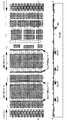
【0039】
図1には、この発明に係るダイナミック型RAMに用いられるセンスアンプ部の一実施例の構成図が示されている。前記7と同様に同図の素子レイアウトパターンでは活性化領域に斜線が付されており、構造断面ではそれと逆に素子分離領域(SGI)に斜線が付されている。ただし、斜線の方向は互いに逆向になっている。この実施例では、図7と同様に同図の上側から順にシェアードスイッチMOSFETQ1−2、プリチャージ回路を構成するMOSFETQ9−11、カラム選択回路を構成するスイッチMOSFETQ12−13、CMOSラッチ回路を構成するp型チャネル増幅MOSFETQ7−8、上記パワースイッチMOSFETQ14とQ15の形成領域を挟んでCMOSラッチ回路を構成するn型チャネル増幅MOSFETQ5−6、及びシェアードスイッチMOSFETQ3−4のように配置される。
【0040】
上記カラムスイッチMOSFETQ12−13とp型チャネルMOSFETQ7−8の間に設けられる活性化領域は、p型チャネルMOSFETが形成される図示しないn型ウェル領域、及びn型チャネルMOSFETが形成される図示しないp型ウェル領域にVDL又はVSSのようなバイアス電圧を与えるコンタクト領域CONTとして用いられる。
【0041】
上記パワースイッチMOSFETQ14とQ15(同図ではそのうちの1つが示されている)は、センスアンプ列に沿ってゲートが延長されるよう、例えば上記シェアードスイッチMOSFETQ1−2等に比べてチャンネル幅が十分に大きく、言い換えるならば、素子サイズが大きく形成されて大きな電流を流すことができるようにされる。このようにセンスアンプを駆動するパワースイッチMOSFETをセンスアンプ列に分散配置した場合には、センスノードとパワースイッチMOSFETとの間の距離が短くでき、サブアレイに設けられる複数のセンスアンプの動作タイミングを相互に均一にすることができるとともに、クロスエリアを他の回路(例えばメイン入出力線のサブ増幅回路)等を設けるために有効利用することができる。
【0042】
図1に示すように、センスアンプを構成するn型チャネルトランジスタ及びp型チャネルトランジスタの活性領域の近傍に別の活性領域が設けられる。つまり、上記各トランジスタQ5−6とQ7−8が隣接する素子分離領域SGIにいわばダミーの活性化領域が応力干渉防止パターンとして設けられる。断面構造において、上記ダミーの活性化領域によってSGIが分断されていることが判る。
【0043】
この実施例のように、センスアンプを構成するトランジスタの活性領域の近傍に別の活性領域(応力干渉防止パターン)を設けると、その周辺からの受ける応力は別に設けた活性領域に影響するものとなる。つまり、センスアンプを構成するトランジスタの活性領域への応力は、別に設けた活性領域との間のSGI応力で殆ど決まることになる。すなわち、この実施例において別に設けた活性領域である応力干渉防止用パターンは、その周辺からの応力差を吸収するような役割を果たすものとなる。
【0044】
当然、センスアンプを構成するトランジスタの活性領域と別に設けた活性領域との間のSGI応力は、活性領域を別に設けない場合より大きくなる。しかしながら、センスアンプを構成するトランジスタの活性領域と別に設けた活性領域との間隔を同じにすれば、センスアンプを構成するトランジスタの活性領域左右で同等の応力(応力中)となって、ペアMOSFETQ5とQ6及びQ7とQ8のVth差を小さくすることができる。この結果、センスアンプのオフセットが低減でき、その分感度が高くなって図3の特性図のように20mV程度までの信号をセンスすることができ、情報保持時間を前記図7のレイアウトの場合に比べて約2倍も長くすることができる。
【0045】
基板表面が(100)面方位から数°オフアングルを持った基板を用いた場合には、図2に示すように、SGI側壁の傾きが上記トランジスタの活性領域の両端で異なるものとなる。この場合には、側壁傾きが大きい方のSGI幅を大きくし、側壁傾きが小さい方のSGI幅を相対的に小さくする。具体的には、上記のようにダミーの活性化領域(応力干渉防止パターン)を設ける位置を調整して、上記トランジスタの活性化領域に対する傾きが大のときには上記SGI幅を大きくし、傾きが小の側ではSGI幅を小さく設定する。
【0046】
この理由は、上記SGIはその密度が粗であるために上記大きな応力を発生させる傾き大のSGIは、その幅を大きくしてSGI自体で発生する応力を小さくする。つまり、SGI自体が応力を吸収してしまうので、その幅を大きくすることで予め発生する応力を小さくしてトランジスタの活性化領域に与える応力を弱めるものである。これに対して、傾き小のSGIでは、SGI幅を相対的に小さくして傾き小に見合った大き目の応力を発生させて、上記活性化領域に与える応力のバランスを採るものである。
【0047】
上記のようにセンスアンプを構成するトランジスタの活性領域の近傍に、その周辺からの応力干渉を少なくするために別の活性領域(応力干渉防止パターン又はダミー活性化領域)を設けことにより、活性領域左右での応力起因のVth差を小さくできる。その分センスアンプの感度を高めることができるので、図3に示したように極端な情報保持時間の短縮を防止できる。その結果、リフレッシュ特性劣化を防止することができる。本願発明者による回路シュミレーションにおいては、図7のようなセンスアンプのレイアウトでは約50mV程度あったペアトランジスタのVth差を20mV程度以内にすることができ、情報保持時間を従来の150msから300msに約2倍に長くすることができた。
【0048】
上記の実施例から得られる作用効果は、下記の通りである。
(1) 差動形態で動作する第1と第2MOSFETとを第1方向に並んで配置し、かかる第1と第2MOSFETからなる組の複数個を上記第1方向と直交する第2方向に配置し、上記第1MOSFETと隣接する第1素子形成領域との間に設けられる第1SGIと、上記第2MOSFETと隣接する2素子形成領域との間に設けられる第2SGIのそれぞれにおいて、上記第1SGIから上記第1MOSFETの素子形成領域に向かう応力と、上記第2SGIから上記第2MOSFETの素子形成領域に向かう応力との差を軽減するように上記第2方向に延長してダミーの素子形成領域を設けて応力干渉防止パターンとしての役割を持たせることにより、上記第1と第2MOSFETからなるペア素子のしきい値電圧差を小さくすることができるという効果が得られる。
【0049】
(2) 上記に加えて、上記第1SGIの上記第1MOSFETの素子形成領域に対する第1側壁の傾きが、上記第2SGIの上記第2MOSFETの素子形成領域に対する第2側壁の傾きより大きいとき、上記第1SGIにおける応力干渉防止用パターンと上記第1側壁との間の幅を、上記第2SGIにおける応力干渉防止用パターンと上記第2側壁との間の幅に比べて大きくすることにより、基板表面が(100)面方位から数°オフアングルを持った基板を用いた場合にも上記第1と第2MOSFETからなるペア素子のしきい値電圧差を小さくすることができるという効果が得られる。
【0050】
(3) 上記に加えて、複数のワード線と複数の相補ビット線対と及びこれらのワード線と相補ビット線対に対応して設けられた複数のダイナミック型メモリセルからなるメモリセルアレイを持つダイナミック型RAMにおいて、上記第1MOSFETと第2MOSFETを、n型チャネルMOSFETにより構成される一対と、p型チャネルMOSFETにより構成される一対とによってCMOSラッチ回路を構成するものとし、上記複数の相補ビット線対の信号を増幅するセンスアンプとすることにより、動作マージンの改善を図ることができるという効果が得られる。
【0051】
(4) 上記に加えて、上記CMOSラッチ回路は上記メモリセルアレイの2つの間に配置し、上記2つのメモリセルアレイの間には、上記CMOSラッチ回路の他に、上記ビット線をプリチャージするプリチャージ回路、上記2つのメモリセルアレイのビット線と上記CMOSラッチ回路の入出力ノードとの間に設けられる選択スイッチ回路、及び上記CMOSラッチ回路の入出力ノードと入出力線との間に設けられるカラムスイッチ回路を設けことにより、高密度の回路レイアウトを実現しつつ、動作マージンの改善、ひいてはメモリセルの情報保持時間を長くすることができるという効果が得られる。
【0052】
以上本発明者よりなされた発明を実施例に基づき具体的に説明したが、本願発明は前記実施例に限定されるものではなく、その要旨を逸脱しない範囲で種々変更可能であることはいうまでもない。例えば、センスアンプは、前記のようなシェアードセンスアンプ方式のものの他、ビット線とセンスアンプとが一対一に対応して設けちらるもの、あるいは1交点方式のものにも同様に適用することができる。この発明に係るペアMOSFET(トランジスタ)は、前記のようなセンスアンプを構成するものの他、多数のペア素子が並んで配置される各種MOSFET回路に広く利用することができる。
【0053】
【発明の効果】
本願において開示される発明のうち代表的なものによって得られる効果を簡単に説明すれば、下記の通りである。差動形態で動作する第1と第2MOSFETとを第1方向に並んで配置し、かかる第1と第2MOSFETからなる組の複数個を上記第1方向と直交する第2方向に配置し、上記第1MOSFETと隣接する第1素子形成領域との間に設けられる第1SGIと、上記第2MOSFETと隣接する2素子形成領域との間に設けられる第2SGIのそれぞれにおいて、上記第1SGIから上記第1MOSFETの素子形成領域に向かう応力と、上記第2SGIから上記第2MOSFETの素子形成領域に向かう応力との差を軽減するように上記第2方向に延長してダミーの素子形成領域を設けて応力干渉防止パターンとしての役割を持たせることにより、上記第1と第2MOSFETからなるペア素子のしきい値電圧差を小さくすることができる。
【図面の簡単な説明】
【図1】この発明に係るダイナミック型RAMに用いられるセンスアンプ部の一実施例を示す構成図である。
【図2】この発明の他の一実施例を示す概略形成領域断面図である。
【図3】この発明を説明するためのメモリセルの情報記憶特性図である。
【図4】この発明が適用されるダイナミック型RAMの一実施例を示す概略レイアウト図である。
【図5】この発明に係るダイナミック型RAMのセンスアンプ部を中心にし一実施例の回路図である。
【図6】この発明が適用されるダイナミック型RAMのセンスアンプ部の一実施例を示す回路図である。
【図7】本願発明に先立って検討された256MビットのDRAMに用いられているセンスアンプ部の構成図である。
【符号の説明】
Q1〜Q20…MOSFET、XDC…Xデコーダ、YDC…Yデコーダ、MA…メインアンプ、MWD…メインワードドライバ、PERI…周辺回路、ROWPDC…X系プリデコーダ回路、ROWRED…X系救済回路、COLPDC…Y系プリデコーダ回路、COLRED…Y系救済回路、
15…サブアレイ、16…センスアンプ領域、17…サブワードドライバ領域、18…交差アリア、51…アドレスバッファ、52…プリデコーダ、11…メインローデコーダ、12…メインワードドライバ、53…カラムデコーダ、61…メインアンプ、62…入力バッファ、63…出力バッファ。[0001]
BACKGROUND OF THE INVENTION
The present invention relates to a semiconductor integrated circuit device and, for example, relates to a technique that is effective when used for an element layout technique of a sense amplifier portion of a dynamic RAM (random access memory).
[0002]
[Prior art]
Some use an SGI (shallow trench insulating layer) as an element isolation region of a dynamic RAM (hereinafter simply referred to as a DRAM) having a storage capacity of 256 Mbits. In SGI, a silicon oxide film (SiO 2) CVD film is formed in a shallow groove and used as an element isolation region. An example of such a DRAM is “VLSI LSI” by Ito, published by Bafukan.
[0003]
[Problems to be solved by the invention]
FIG. 7 shows the arrangement of the active region and the gate electrode of the sense amplifier unit used in the 256 Mbit DRAM studied prior to the present invention. In this arrangement, in both the region where the n-type channel transistor is formed and the region where the p-type channel transistor is formed, the arrangement of the element isolation region and another active region is different on the left and right of the active region. That is, in the n-type channel transistor, a shared switch transistor is disposed between the n-type channel transistor and the memory cell, and a power switch transistor is disposed on the other side. In the p-type channel transistor, the power switch transistor is arranged between the p-type channel transistor and the n-type channel transistor, and the transistor constituting the precharge circuit is arranged on the other side.
[0004]
In the element layout pattern of the same figure, the activation region is hatched, and in the structure cross section, the element isolation region (SGI) is hatched. However, the directions of the diagonal lines are opposite to each other. Since the compressive stress from the SGI varies depending on the element isolation width and its arrangement, the compressive stress applied to the region where the n-type channel transistor is formed and the region where the p-type channel transistor is formed depends on the left and right sides of the active region. Will be different. Usually, the characteristics of a silicon crystal change depending on the compressive stress, and when viewed as an influence on the threshold voltage (hereinafter referred to as Vth), Vth decreases by about 10 and several mV at a compressive stress of 100 Mpa.
[0005]
Therefore, if a difference in compressive stress occurs between the left and right sides of the active region, a Vth difference occurs in the pair transistors. The Vth difference directly decreases the sensitivity of the sense amplifier. For example, when the charge accumulated in the capacitor is reduced by the junction leakage current and the charge amount changes with time as shown by the solid line in FIG. 3, the signal voltage appearing on the bit line selected when the word line is selected is shown in FIG. The change with time as shown by the solid line in FIG. Here, the elapsed time is the time from when information is written to the capacitor to when the word line is set in a non-selected state until when it is selected. That is, the time when the sensitivity of the sense amplifier matches the signal voltage corresponds to the information holding time.
[0006]
When the Vth difference as described above becomes the sense sensitivity as it is, the information holding time is shortened as shown in FIG. As a result, the cycle required for refreshing must be halved, and the refresh characteristics are degraded. As described above, when the device is further miniaturized, the Vth difference between the pair transistors increases due to the influence of the SGI stress, and the pair transistors are offset. It has been clarified by a study by the inventors of the present application that the refresh characteristics are rapidly deteriorated.
[0007]
An object of the present invention is to provide a semiconductor integrated circuit device having a pair transistor in which the influence of SGI stress is reduced. Another object of the present invention is to provide a semiconductor integrated circuit device having a pair transistor in which an element is miniaturized and an operation margin is improved. The above and other objects and novel features of the present invention will be apparent from the description of this specification and the accompanying drawings.
[0008]
[Means for Solving the Problems]
The outline of typical inventions disclosed in the present application will be briefly described as follows.. C In a DRAM having a sense amplifier having a MOS latch circuitThe second It is provided side by side in one directionn-type channel MOSFET First MOSFETand Second MOSFET setBut ,A plurality are arranged in a second direction orthogonal to the first direction. First element formation regionAnd above Adjacent to the first element formation region in the first directionDo Between the second element formation regionBe provided 1st SGIWhen The first element forming region is adjacent to the first element forming region on the side opposite to the second element forming region in the first direction.Do Between the third element formation regionBe provided Second SGIWhen ,A set of a third MOSFET and a fourth MOSFET, which are adjacent to the third element formation region via the third SGI in the first direction and are arranged side by side in the first direction and are formed of p-type channel MOSFETs, are arranged in the second direction. A plurality of fourth element formation regions, the fourth element formation region, and a fifth element formation region adjacent to the fourth element formation region on the opposite side of the third element formation region in the first direction. A first dummy element forming region provided along the second direction on the first SGI, and a second dummy element provided along the second direction on the second SGI. A formation region; a third dummy element formation region provided in the third SGI along the second direction; and a fourth dummy element formation region provided in the fourth SGI along the second direction. And the set of the first MOSFET and the second MOSFET provided in the first element formation region and the set of the third MOSFET and the fourth MOSFET provided in the fourth element formation region constitute a CMOS latch circuit. The stress from the first SGI to the first element formation region and the stress from the second SGI to the first element formation region are reduced, and the stress from the third SGI to the fourth element formation region is reduced. And the difference between the stress from the fourth SGI toward the fourth element formation region is reduced. DRAM.
[0009]
DETAILED DESCRIPTION OF THE INVENTION
FIG. 4 is a schematic layout diagram showing an embodiment of a dynamic RAM to which the present invention is applied. Each circuit block shown in the figure is formed on one semiconductor substrate such as single crystal silicon by a known semiconductor integrated circuit manufacturing technique. Each circuit in the figure is drawn almost in accordance with the geometrical arrangement on the semiconductor substrate. In this embodiment, the memory array is divided into four as a whole and constitutes memory banks (Banks) 0 to 3.
[0010]
The memory banks 0 to 3 correspond to a memory array that is divided into two vertically and two horizontally along the longitudinal direction of the semiconductor chip. A peripheral circuit PERI including an address input circuit, a data input / output circuit, and a bonding pad row is provided at a central portion along the longitudinal direction of the chip. The peripheral circuit PERI is not particularly limited, but the random logic circuit and the bonding pad are arranged side by side in order to rationalize the layout of each circuit composed of the random logic circuit.
[0011]
Although not shown in the figure, examples of the peripheral circuit PERI include a boosted voltage generating circuit, a control circuit for controlling the operation thereof, and a reference voltage for an input circuit configured by a differential circuit by dividing the external power supply voltage VDDQ by half. Voltage divider circuit, input / output circuit and its clock control circuit, Y predecoder and read / write buffer, step-down circuit for forming peripheral circuit operating voltage, and detecting whether VPP voltage is a desired voltage VPP sensor, stabilization capacitor for stabilizing the step-down voltage VPERI, X address latch circuit, Y clock circuit, mode decoder / clock buffer and command circuit, Y counter and its control circuit, refresh control circuit, bonding option circuit, power-on There are detection circuits and the like.
[0012]
As described above, in each memory array, which is divided into two pieces in the vertical direction along the longitudinal direction of the semiconductor chip and two pieces in the left and right direction, a total of four memory arrays, the X system is located in the middle portion in the horizontal direction with respect to the longitudinal direction. The predecoder circuit ROWDC and the relief circuit ROWRED, the Y-system predecoder circuit COLPDC, and the relief circuit COLRED are arranged together. That is, the X-system predecoder circuit ROWDC and the relief circuit ROWRED, the Y-system predecoder circuit COLPDC, and the relief circuit COLRED correspond to the four memory arrays, respectively, and correspond to the memory array in which the left and right two are provided. 2 sets are distributed and provided.
[0013]
A main word driver region MWD is formed along the intermediate portion of the memory array in the same manner as described above, and each main word line provided to extend downward and upward corresponding to each memory array is driven. To be done. In this configuration, when the same subarray is used, the main word line is extended so as to penetrate 16 subarrays. Although not particularly limited, in the memory array, a Y decoder YDC is provided on the chip peripheral side opposite to the chip central portion.
[0014]
The four divided memory arrays are sandwiched between the main amplifier MA arranged on the central side and the Y decoder YDC arranged on the peripheral side. In this case, a portion where the wiring channels extending in the vertical direction and the horizontal direction intersect is generated in the center portion of the chip, and although not particularly limited, the stabilization capacitor C is formed there. In addition, a stabilizing capacitor having a small capacitance value is provided as appropriate by being dispersed in gaps such as peripheral circuits.
[0015]
In this embodiment, the memory arrays divided into four are arranged so as to be sandwiched between the main amplifier MA arranged on the center side and the Y decoder YDC arranged on the peripheral side. The memory array is divided into a plurality of
[0016]
Although not illustrated, one
[0017]
A sub word driver (sub word line drive circuit) 17 is provided for each divided
[0018]
In the case of adopting the layout as shown in FIG. 4, when a Y address is input, a Y circuit disposed on the peripheral side of the chip via a relief circuit and a predecoder provided in the intermediate portion of the memory array through the address buffer. This is transmitted to the decoder YDC, where a Y selection signal is formed. A complementary bit line of one sub-array is selected from the Y selection signal, transmitted to the main amplifier MA on the chip center side opposite to the sub-array, amplified and output through an output circuit (not shown).
[0019]
At first glance, this configuration is determined so that the time from when the signal is routed around the chip until the read signal is output becomes longer. However, since it is necessary to input the address signal as it is to the relief circuit, if the relief circuit is arranged at one of the center of the chip, the output time of the predecoder is determined based on the determination result of whether it is a defective address or not. Is done. That is, if the predecoder and the relief circuit are separated from each other, the signal delay at that point causes the actual Y selection operation to be delayed.
[0020]
In this embodiment, since the main amplifier MA and the Y decoder YDC are arranged on both sides of the memory array, a signal transmission path for selecting a complementary bit line of the subarray and an input / output line from the selected complementary bit line The sum of the signal transmission path passing through the main amplifier MA and the input of the main amplifier MA is half that of one round trip as described above as a signal transmission path that only crosses the memory array regardless of which complementary bit line is selected. It can be shortened. As a result, the memory access speed can be increased.
[0021]
FIG. 5 shows a circuit diagram of a simplified embodiment from address input to data output, centering on the sense amplifier portion of the dynamic RAM according to the present invention. In the figure, a
[0022]
As the dynamic memory cell, one of the dynamic memory cells provided between the sub word line SWL provided in the one subarray 15 and one of the complementary bit lines BL and BLB is exemplarily shown as a representative. ing. The dynamic memory cell includes an address selection MOSFET Qm and a storage capacitor Cs. The gate of the address selection MOSFET Qm is connected to the sub word line SWL, the drain of the MOSFET Qm is connected to the bit line BL, and the storage capacitor Cs is connected to the source. The other electrode of the storage capacitor Cs is made common to receive the plate voltage VPLT. A negative back bias voltage VBB is applied to the substrate (channel) of the MOSFET Qm. Although not particularly limited, the back bias voltage VBB is set to a voltage such as −1V. The selection level of the sub word line SWL is set to a high voltage VPP that is higher than the high level of the bit line by the threshold voltage of the address selection MOSFET Qm.
[0023]
When the sense amplifier is operated at the internal step-down voltage VDL, the high level amplified by the sense amplifier and applied to the bit line is set to the internal voltage VDL level. Therefore, the high voltage VPP corresponding to the selection level of the word line is set to VDL + Vth + α. A pair of complementary bit lines BL and BLB in the sub-array provided on the left side of the sense amplifier are arranged in parallel as shown in FIG. The complementary bit lines BL and BLB are connected to input / output nodes of the unit circuit of the sense amplifier by shared switch MOSFETs Q1 and Q2.
[0024]
The unit circuit of the sense amplifier is constituted by a CMOS latch circuit comprising n-type channel amplification MOSFETs Q5 and Q6 and p-type channel amplification MOSFETs Q7 and Q8, which are latched by crossing gates and drains. The sources of n-type channel MOSFETs Q5 and Q6 are connected to a common source line CSN. The sources of p-type channel MOSFETs Q7 and Q8 are connected to a common source line CSP. A power switch MOSFET is connected to each of the common source lines CSN and CSP. The common source line CSN to which the sources of the n-type channel amplification MOSFETs Q5 and Q6 are connected is supplied with an operating voltage corresponding to the ground potential by the n-type channel power switch MOSFET Q14.
[0025]
Although not particularly limited, the common source line CSP to which the sources of the p-type channel amplification MOSFETs Q7 and Q8 are connected is provided with an n-type channel power MOSFET Q15 for supplying the internal voltage VDL. A high level of the sense amplifier activation signal SAP supplied to the gate of the n-type channel power MOSFET Q15 is a signal of the boosted voltage VPP level. That is, since the boosted voltage VPP is about 3.6 V, the n-type channel MOSFET Q15 can be sufficiently turned on to output a voltage corresponding to the internal voltage VDL from the source side.
[0026]
At the input / output node of the unit circuit of the sense amplifier, there are provided an equalize MOSFET Q11 for short-circuiting the complementary bit line and a precharge (equalize) circuit comprising switch MOSFETs Q9 and Q10 for supplying a half precharge voltage VBLR to the complementary bit line. . The gates of these MOSFETs Q9 to Q11 are commonly supplied with a precharge signal PCB. Although not shown, the driver circuit for forming the precharge signal PCB is provided with an inverter circuit in the cross area so as to make the rise and rise fast. That is, at the start of memory access, the MOSFETs Q9 to Q11 constituting the precharge circuit are switched at high speed through the inverter circuits distributed in the respective cross areas prior to the word line selection timing.
[0027]
In the
[0028]
The unit circuit of the sense amplifier is connected to similar complementary bit lines BL and BLB of the
[0029]
As a result, the input / output node of the sense amplifier is connected to the upper complementary bit lines BL and BLB to amplify a minute signal of the memory cell connected to the selected sub word line SWL, and the column switch circuit (Q12 And Q13) to the local input / output lines LIO1 and LIO1B. The local input / output lines LIO1 and LIO1B extend along the sense amplifier row, that is, in the horizontal direction in FIG. The local input / output lines LIO1 and LIO1B are connected to main input / output lines MIO and MIOB to which the input terminals of the
[0030]
The IO switch circuit is switch-controlled by a selection signal formed by decoding an X-system address signal. The IO switch circuit may have a CMOS switch configuration in which a p-type channel MOSFET is connected in parallel to each of the n-type channel MOSFETs Q19 and Q20. In the burst mode of the synchronous DRAM, the column selection signal YS is switched by a counter operation, and the connection between the local input / output lines LIO1, LIO1B and LIO2, LIO2B and two pairs of complementary bit lines BL and BLB in sequence is sequentially performed. Can be switched to.
[0031]
The address signal Ai is supplied to the
[0032]
The
[0033]
Although not particularly limited, the power supply voltage VDDQ supplied from the external terminal is set to 3.3 V in the first embodiment, the step-down voltage VPERI (VDD) supplied to the internal circuit is set to 2.5 V, and the sense The operating voltage VDL of the amplifier is 1.8V. The word line selection signal (boosted voltage) is set to 3.6V. The bit line precharge voltage VBLR is set to 0.9 V corresponding to VDL / 2, and the plate voltage VPLT is also set to 0.9 V. The substrate voltage VBB is set to -1.0V. The power supply voltage VDDQ supplied from the external terminal may be set to a low voltage such as 2.5V as the second form. In such a low power supply voltage VDDQ, the step-down voltage VPERI (VDD) and the step-down voltage VDL may be set to about 1.8V.
[0034]
Alternatively, the power supply voltage VDDQ supplied from the external terminal is set to 3.3 V, and the step-down voltage VPERI (VDD) supplied to the internal circuit and the operating voltage VDL of the sense amplifier are set to 2.0 V or 1.8 V, respectively. May be. As described above, the internal voltage with respect to the external power supply voltage VDDQ can take various embodiments.
[0035]
FIG. 6 is a circuit diagram showing one embodiment of a sense amplifier portion of a dynamic RAM to which the present invention is applied. The circuit symbols attached to the MOSFETs of this embodiment correspond to those shown in FIG. As described above, the unit circuit of the sense amplifier is composed of n-type channel MOSFETs Q5 and Q6 and p-type channel MOSFETs Q7 and Q8. The sources of these latch-type n-type channel MOSFETs Q5 and Q6 and p-type channel MOSFETs Q7 and Q8 are n-type channel MOSFETs and p-type channels constituting other similar sense amplifiers (not shown) provided corresponding to the same subarray. The sources of the MOSFETs are connected to common source lines CSN and CSP that are commonly connected to each other.
[0036]
The common source line CSN is supplied with an operating voltage VSSA via an n-type channel MOSFET Q14 receiving a timing signal SAN, and the common source line CSP is supplied with an operating voltage VDL via an n-type channel MOSFET Q15 receiving a timing signal SAP. Is supplied. In this embodiment, the ground potential VSSA, which is one operating voltage of the sense amplifier, is separated from the ground potential VSS so as not to be affected by noise from the peripheral circuit or the like. The ground potential supplied from the external terminal is applied. That is, the ground potential VSSA applied to the sense amplifier is directly applied from the external terminal by a wiring provided separately from the peripheral circuit and the input / output circuit.
[0037]
A pair of input / output nodes (sense nodes) SAT and SAB of the latch circuit are pre-configured by an equalize MOSFET Q11 for short-circuiting them and a precharge MOSFET Q9 and Q10 for transmitting a half precharge voltage VBLR to the sense nodes SAT and SAB. A charge circuit is provided. The sense nodes SAT and SAB are connected to the local input / output lines LIOT and LIOB via column switch MOSFETs Q12 and Q13 whose gates are supplied with a column selection signal YS. The column selection signal YS is supplied in common to the selection switch MOSFETs corresponding to four pairs of LIOs, although not particularly limited. Then, shared switch MOSFETs Q1 and Q2 are provided between the complementary bit lines BLLT and BLLB provided on the left side of the sense amplifier section, and between the complementary bit lines BLRT and BLRB provided on the right side. Shared switch MOSFETs Q3 and Q4 are provided.
[0038]
A control signal SHL is supplied to the gates of the shared switch MOSFETs Q1 and Q2, and a control signal SHR is supplied to the gates of the shared switch MOSFETs Q3 and Q4. A dynamic type memory comprising the address selection MOSFET Qm and the storage capacitor Cs at the intersections of the complementary bit lines BLLT and BLLB on the left side of the sense amplifier section and the sub word lines SWL1, SWL2, etc. arranged so as to be orthogonal thereto. A cell is provided. Similarly, the address selection MOSFET Qm and the storage capacitor Cs are formed at the intersections of the complementary bit lines BLRT and BLRB on the right side of the sense amplifier section and the sub word lines SWL3 and SWL4 arranged so as to be orthogonal thereto. A dynamic memory cell is provided.
[0039]
FIG. 1 shows a configuration diagram of an embodiment of a sense amplifier unit used in a dynamic RAM according to the present invention. As in the case of 7, the active region is hatched in the element layout pattern shown in FIG. 7, and the element isolation region (SGI) is hatched in the structure cross section. However, the directions of the diagonal lines are opposite to each other. In this embodiment, in the same manner as in FIG. 7, the shared switch MOSFET Q1-2, the MOSFET Q9-11 constituting the precharge circuit, the switch MOSFET Q12-13 constituting the column selection circuit, and the p constituting the CMOS latch circuit are sequentially arranged from the upper side of FIG. A type channel amplification MOSFET Q7-8, an n type channel amplification MOSFET Q5-6 constituting a CMOS latch circuit across the formation region of the power switch MOSFETs Q14 and Q15, and a shared switch MOSFET Q3-4 are arranged.
[0040]
The activation region provided between the column switch MOSFET Q12-13 and the p-type channel MOSFET Q7-8 includes an n-type well region (not shown) in which a p-type channel MOSFET is formed and a p (not shown) in which an n-type channel MOSFET is formed. It is used as a contact region CONT that gives a bias voltage such as VDL or VSS to the type well region.
[0041]
The power switch MOSFETs Q14 and Q15 (one of which is shown in the figure) have a channel width sufficiently larger than that of the shared switch MOSFET Q1-2, for example, so that the gate is extended along the sense amplifier row. In other words, in other words, the element size is made large so that a large current can flow. When the power switch MOSFETs for driving the sense amplifiers are distributed in the sense amplifier row in this way, the distance between the sense nodes and the power switch MOSFETs can be shortened, and the operation timings of the plurality of sense amplifiers provided in the subarray can be set. The cross areas can be made uniform, and the cross area can be effectively used for providing other circuits (for example, a sub-amplifier circuit for a main input / output line).
[0042]
As shown in FIG. 1, another active region is provided in the vicinity of the active regions of the n-type channel transistor and the p-type channel transistor constituting the sense amplifier. That is, a dummy activation region is provided as a stress interference prevention pattern in the element isolation region SGI where the transistors Q5-6 and Q7-8 are adjacent to each other. In the cross-sectional structure, it can be seen that the SGI is divided by the dummy activation region.
[0043]
When another active region (stress interference prevention pattern) is provided in the vicinity of the active region of the transistor constituting the sense amplifier as in this embodiment, the stress received from the periphery affects the active region provided separately. Become. That is, the stress on the active region of the transistor constituting the sense amplifier is almost determined by the SGI stress between the active region provided separately. That is, the stress interference prevention pattern, which is an active region separately provided in this embodiment, plays a role of absorbing a stress difference from the periphery.
[0044]
Naturally, the SGI stress between the active region of the transistor constituting the sense amplifier and the active region provided separately is larger than when the active region is not provided separately. However, if the distance between the active region of the transistor constituting the sense amplifier and the active region provided separately is the same, the pair MOSFET Q5 has the same stress (during stress) on the left and right of the active region of the transistor constituting the sense amplifier. And Vth difference between Q6 and Q7 and Q8 can be reduced. As a result, the offset of the sense amplifier can be reduced, the sensitivity is increased correspondingly, and a signal up to about 20 mV can be sensed as shown in the characteristic diagram of FIG. 3, and the information holding time is set in the case of the layout of FIG. It can be about twice as long.
[0045]
When a substrate having a substrate surface with an off-angle of several degrees from the (100) plane orientation is used, as shown in FIG. 2, the slope of the SGI side wall differs at both ends of the active region of the transistor. In this case, the SGI width with the larger side wall inclination is increased, and the SGI width with the smaller side wall inclination is relatively decreased. Specifically, the position where the dummy activation region (stress interference prevention pattern) is provided as described above is adjusted, and when the inclination of the transistor with respect to the activation region is large, the SGI width is increased and the inclination is reduced. On the side, the SGI width is set small.
[0046]
The reason is that the SGI having a large slope that generates the large stress because the density of the SGI is coarse increases the width of the SGI to reduce the stress generated in the SGI itself. That is, since SGI itself absorbs stress, increasing the width reduces the stress generated in advance and weakens the stress applied to the active region of the transistor. On the other hand, in the SGI having a small inclination, the SGI width is made relatively small to generate a large stress corresponding to the small inclination, and the stress applied to the activated region is balanced.
[0047]
By providing another active region (stress interference prevention pattern or dummy activation region) in the vicinity of the active region of the transistor constituting the sense amplifier as described above in order to reduce stress interference from the periphery thereof, the active region The difference in Vth caused by stress on the left and right can be reduced. As a result, the sensitivity of the sense amplifier can be increased, so that it is possible to prevent an extremely short information holding time as shown in FIG. As a result, it is possible to prevent the refresh characteristics from being deteriorated. In the circuit simulation by the inventor of the present application, the Vth difference of the pair transistors, which was about 50 mV in the layout of the sense amplifier as shown in FIG. 7, can be within about 20 mV, and the information holding time is reduced from the conventional 150 ms to 300 ms. The length could be doubled.
[0048]
The effects obtained from the above embodiment are as follows.
(1) First and second MOSFETs operating in a differential mode are arranged side by side in a first direction, and a plurality of sets of the first and second MOSFETs are arranged in a second direction orthogonal to the first direction. In each of the first SGI provided between the first MOSFET and the first element forming region adjacent to the first MOSFET and the second SGI provided between the second element forming region adjacent to the second MOSFET and the first SGI, In order to reduce the difference between the stress toward the element formation region of the first MOSFET and the stress from the second SGI toward the element formation region of the second MOSFET, a dummy element formation region is provided extending in the second direction to reduce the stress. By providing a role as an interference prevention pattern, it is possible to reduce the threshold voltage difference of the pair element composed of the first and second MOSFETs. The effect that it can be obtained.
[0049]
(2) In addition to the above, when the inclination of the first sidewall with respect to the element formation region of the first MOSFET of the first SGI is larger than the inclination of the second sidewall with respect to the element formation region of the second MOSFET of the second SGI, By making the width between the stress interference prevention pattern in 1 SGI and the first side wall larger than the width between the stress interference prevention pattern in the second SGI and the second side wall, the substrate surface becomes ( 100) Even when a substrate having an off-angle of several degrees from the plane orientation is used, the effect that the threshold voltage difference between the paired elements composed of the first and second MOSFETs can be reduced can be obtained.
[0050]
(3) In addition to the above, a dynamic having a memory cell array composed of a plurality of word lines, a plurality of complementary bit line pairs, and a plurality of dynamic memory cells provided corresponding to these word lines and the complementary bit line pairs. In the type RAM, the first MOSFET and the second MOSFET are composed of a pair constituted by an n-type channel MOSFET and a pair constituted by a p-type channel MOSFET to constitute a CMOS latch circuit, and the plurality of complementary bit line pairs By using a sense amplifier that amplifies the above signal, an effect of improving the operation margin can be obtained.
[0051]
(4) In addition to the above, the CMOS latch circuit is disposed between two of the memory cell arrays, and in addition to the CMOS latch circuit, a precharge for precharging the bit line is provided between the two memory cell arrays. A charge switch; a selection switch circuit provided between the bit line of the two memory cell arrays and the input / output node of the CMOS latch circuit; and a column provided between the input / output node of the CMOS latch circuit and the input / output line. By providing the switch circuit, the effect of improving the operation margin and extending the information holding time of the memory cell can be obtained while realizing a high-density circuit layout.
[0052]
The invention made by the inventor has been specifically described based on the embodiments. However, the invention of the present application is not limited to the embodiments, and various modifications can be made without departing from the scope of the invention. Nor. For example, in addition to the shared sense amplifier type as described above, the sense amplifier can be similarly applied to a type in which bit lines and sense amplifiers are provided in a one-to-one correspondence or a one-intersection type. it can. The pair MOSFET (transistor) according to the present invention can be widely used in various MOSFET circuits in which a large number of pair elements are arranged side by side, in addition to those constituting the sense amplifier as described above.
[0053]
【The invention's effect】
The effects obtained by the representative ones of the inventions disclosed in the present application will be briefly described as follows. The first and second MOSFETs operating in a differential mode are arranged side by side in the first direction, and a plurality of sets of the first and second MOSFETs are arranged in a second direction orthogonal to the first direction, In each of the first SGI provided between the first MOSFET and the first element formation region adjacent to the first MOSFET and the second SGI provided between the second MOSFET and the two element formation regions adjacent to each other, the first SGI to the first MOSFET A stress interference prevention pattern is provided by providing a dummy element formation region extending in the second direction so as to reduce the difference between the stress toward the element formation region and the stress from the second SGI toward the element formation region of the second MOSFET. Thus, the threshold voltage difference between the paired elements composed of the first and second MOSFETs can be reduced.
[Brief description of the drawings]
FIG. 1 is a block diagram showing an embodiment of a sense amplifier unit used in a dynamic RAM according to the present invention.
FIG. 2 is a schematic sectional view of a forming region showing another embodiment of the present invention.
FIG. 3 is an information storage characteristic diagram of a memory cell for explaining the present invention.
FIG. 4 is a schematic layout diagram showing one embodiment of a dynamic RAM to which the present invention is applied.
FIG. 5 is a circuit diagram of an embodiment centering on a sense amplifier portion of a dynamic RAM according to the present invention;
FIG. 6 is a circuit diagram showing an embodiment of a sense amplifier portion of a dynamic RAM to which the present invention is applied.
FIG. 7 is a configuration diagram of a sense amplifier unit used in a 256 Mbit DRAM studied prior to the present invention.
[Explanation of symbols]
Q1 to Q20 ... MOSFET, XDC ... X decoder, YDC ... Y decoder, MA ... main amplifier, MWD ... main word driver, PERI ... peripheral circuit, ROWPDC ... X system predecoder circuit, ROWRED ... X system relief circuit, COLPDC ... Y System predecoder circuit, COLRED ... Y system relief circuit,
DESCRIPTION OF
Claims (3)
Translated fromJapanese第1方向に並んで設けられn型チャネルMOSFETからなる第1MOSFETおよび第2MOSFETの組が、上記第1方向に直交する第2方向に複数配置される第1素子形成領域と、
上記第1素子形成領域に対し上記第1方向に隣接する第2素子形成領域との間に設けられる第1SGIと、
上記第1素子形成領域と、上記第1素子形成領域に対し上記第2素子形成領域とは反対側に上記第1方向に隣接する第3素子形成領域との間に設けられる第2SGIと、
上記第3素子形成領域に対し第3SGIを介して上記第1方向に隣接し、上記第1方向に並んで設けられp型チャネルMOSFETからなる第3MOSFETおよび第4MOSFETの組が、上記第2方向に複数配置される第4素子形成領域と、
上記第4素子形成領域と、上記第4素子形成領域に対し上記第3素子形成領域とは反対側に上記第1方向に隣接する第5素子形成領域との間に設けられる第4SGIと、
上記第1SGIに、上記第2方向に沿って設けられる第1ダミー素子形成領域と、
上記第2SGIに、上記第2方向に沿って設けられる第2ダミー素子形成領域と、
上記第3SGIに、上記第2方向に沿って設けられる第3ダミー素子形成領域と、
上記第4SGIに、上記第2方向に沿って設けられる第4ダミー素子形成領域と、
を備え、
上記第1素子形成領域に設けられる上記第1MOSFETおよび上記第2MOSFETの組と、上記第4素子形成領域に設けられる上記第3MOSFETおよび上記第4MOSFETの組とは、CMOSラッチ回路を構成し、
上記第1SGIから上記第1素子形成領域に向かう応力と、上記第2SGIから上記第1素子形成領域に向かう応力との差を軽減するとともに、上記第3SGIから上記第4素子形成領域に向かう応力と、上記第4SGIから上記第4素子形成領域に向かう応力との差を軽減する、ことを特徴とするDRAM。In a DRAM having a sense amplifier having a CMOS latch circuit,
A first element forming region in which a plurality of sets of first MOSFETs and second MOSFETs, which are arranged in the first direction and are formed of n-type channel MOSFETs, are arranged in a second direction orthogonal to the first direction;
A first SGI provided between the first element formation region and the second element formation region adjacent in the first direction;
A second SGI provided between the first element formation region and a third element formation region adjacent to the first element formation region on the opposite side of the second element formation region in the first direction;
A set of a third MOSFET and a fourth MOSFET, which are adjacent to the third element formation region via the third SGI in the first direction and are arranged side by side in the first direction and are formed of p-type channel MOSFETs, are arranged in the second direction. A plurality of fourth element formation regions disposed;
A fourth SGI provided between the fourth element formation region and a fifth element formation region adjacent to the fourth element formation region on the opposite side of the third element formation region in the first direction;
A first dummy element formation region provided along the second direction in the first SGI;
A second dummy element formation region provided in the second SGI along the second direction;
A third dummy element formation region provided in the third SGI along the second direction;
A fourth dummy element formation region provided in the fourth SGI along the second direction;
Equipped witha,
The set of the first MOSFET and the second MOSFET provided in the first element formation region and the set of the third MOSFET and the fourth MOSFET provided in the fourth element formation region constitute a CMOS latch circuit,
While reducing the difference between the stress from the first SGI toward the first element formation region and the stress from the second SGI toward the first element formation region, the stress from the third SGI toward the fourth element formation region A DRAM thatreduces a difference from a stress directed from the fourth SGI toward the fourth element formation region .
上記第1ダミー素子形成領域および上記第2ダミー素子形成領域と、上記第1素子形成領域との各々の間隔が等しくなるように配置されると共に、
上記第3ダミー素子形成領域および上記第4ダミー素子形成領域と、上記第4素子形成領域との各々の間隔が等しくなるように配置されることを特徴とするDRAM。In claim1 ,
The first dummy element formation region, the second dummy element formation region, and the first element formation region are arranged so that the distance between them is equal,
A DRAM, wherein the third dummy element formation region, the fourth dummy element formation region, and the fourth element formation region are arranged to have equal intervals.
上記第2素子形成領域にはシェアードスイッチMOSFETが、上記第3素子形成領域にはパワースイッチMOSFETが、上記第5素子形成領域にはコンタクト用活性化領域が、各々配置されることを特徴とするDRAM。In claim1 ,
A shared switch MOSFET is disposed in the second element formation region, a power switch MOSFET is disposed in the third element formation region, and a contact activation region is disposed in the fifth element formation region. DRAM.
Priority Applications (1)
| Application Number | Priority Date | Filing Date | Title |
|---|---|---|---|
| JP2000147157AJP4767390B2 (en) | 2000-05-19 | 2000-05-19 | DRAM |
Applications Claiming Priority (1)
| Application Number | Priority Date | Filing Date | Title |
|---|---|---|---|
| JP2000147157AJP4767390B2 (en) | 2000-05-19 | 2000-05-19 | DRAM |
Publications (2)
| Publication Number | Publication Date |
|---|---|
| JP2001332706A JP2001332706A (en) | 2001-11-30 |
| JP4767390B2true JP4767390B2 (en) | 2011-09-07 |
Family
ID=18653372
Family Applications (1)
| Application Number | Title | Priority Date | Filing Date |
|---|---|---|---|
| JP2000147157AExpired - Fee RelatedJP4767390B2 (en) | 2000-05-19 | 2000-05-19 | DRAM |
Country Status (1)
| Country | Link |
|---|---|
| JP (1) | JP4767390B2 (en) |
Families Citing this family (12)
| Publication number | Priority date | Publication date | Assignee | Title |
|---|---|---|---|---|
| JP4068340B2 (en)* | 2001-12-17 | 2008-03-26 | エルピーダメモリ株式会社 | Semiconductor integrated circuit device |
| JP4504633B2 (en)* | 2003-05-29 | 2010-07-14 | パナソニック株式会社 | Semiconductor integrated circuit device |
| JP2005286341A (en) | 2004-03-30 | 2005-10-13 | Samsung Electronics Co Ltd | Low noise and high performance LSI device, layout and manufacturing method thereof |
| JP4528561B2 (en)* | 2004-06-23 | 2010-08-18 | パナソニック株式会社 | Semiconductor device and manufacturing method of semiconductor device |
| JP4833544B2 (en) | 2004-12-17 | 2011-12-07 | パナソニック株式会社 | Semiconductor device |
| US8350330B2 (en) | 2008-05-08 | 2013-01-08 | Taiwan Semiconductor Manufacturing Company, Ltd. | Dummy pattern design for reducing device performance drift |
| US7958465B2 (en) | 2008-05-08 | 2011-06-07 | Taiwan Semiconductor Manufacturing Company, Ltd. | Dummy pattern design for reducing device performance drift |
| JP5676075B2 (en)* | 2008-11-17 | 2015-02-25 | ピーエスフォー ルクスコ エスエイアールエルPS4 Luxco S.a.r.l. | Semiconductor device |
| JP5147654B2 (en)* | 2008-11-18 | 2013-02-20 | パナソニック株式会社 | Semiconductor device |
| US9646958B2 (en)* | 2010-03-17 | 2017-05-09 | Taiwan Semiconductor Manufacturing Company, Ltd. | Integrated circuits including dummy structures and methods of forming the same |
| JP6373441B2 (en)* | 2017-04-11 | 2018-08-15 | ルネサスエレクトロニクス株式会社 | Semiconductor memory |
| CN112840568A (en)* | 2018-10-25 | 2021-05-25 | 株式会社半导体能源研究所 | Detection device, semiconductor device |
Family Cites Families (5)
| Publication number | Priority date | Publication date | Assignee | Title |
|---|---|---|---|---|
| TW299458B (en)* | 1994-11-10 | 1997-03-01 | Intel Corp | |
| JP3604482B2 (en)* | 1995-12-25 | 2004-12-22 | 松下電器産業株式会社 | Semiconductor device and method of manufacturing semiconductor device |
| JPH10173035A (en)* | 1996-12-10 | 1998-06-26 | Hitachi Ltd | Semiconductor integrated circuit device and its design method |
| JPH1116999A (en)* | 1997-06-27 | 1999-01-22 | Hitachi Ltd | Semiconductor integrated circuit device, method of manufacturing the same, and method of designing the same |
| JPH11307741A (en)* | 1998-04-27 | 1999-11-05 | Hitachi Ltd | Semiconductor storage device |
- 2000
- 2000-05-19JPJP2000147157Apatent/JP4767390B2/ennot_activeExpired - Fee Related
Also Published As
| Publication number | Publication date |
|---|---|
| JP2001332706A (en) | 2001-11-30 |
Similar Documents
| Publication | Publication Date | Title |
|---|---|---|
| JP3853513B2 (en) | Dynamic RAM | |
| JP4427847B2 (en) | Dynamic RAM and semiconductor device | |
| JP5248019B2 (en) | Semiconductor memory device and sense amplifier circuit thereof | |
| KR101070552B1 (en) | Semiconductor memory device | |
| JP4552258B2 (en) | Semiconductor memory device | |
| US20070139995A1 (en) | Semiconductor memory device | |
| TWI783687B (en) | Memory subword driver circuits and layout | |
| JP2005340367A (en) | Semiconductor integrated circuit device | |
| JP4079522B2 (en) | Semiconductor integrated circuit device | |
| JP4767390B2 (en) | DRAM | |
| US11778813B2 (en) | Memory subword driver layout | |
| JP4487227B2 (en) | Dynamic RAM | |
| WO1999000846A1 (en) | Semiconductor integrated circuit device | |
| JP2000036193A (en) | Semiconductor integrated circuit device | |
| JP4243389B2 (en) | Semiconductor memory device and semiconductor device | |
| JP2010211892A (en) | Semiconductor device | |
| JP2000090663A (en) | Dynamic RAM | |
| JPH1186554A (en) | Dynamic RAM | |
| JPH11307739A (en) | Dynamic RAM | |
| JP2010182419A (en) | Semiconductor memory device |
Legal Events
| Date | Code | Title | Description |
|---|---|---|---|
| A711 | Notification of change in applicant | Free format text:JAPANESE INTERMEDIATE CODE: A711 Effective date:20060706 | |
| A621 | Written request for application examination | Free format text:JAPANESE INTERMEDIATE CODE: A621 Effective date:20061207 | |
| A977 | Report on retrieval | Free format text:JAPANESE INTERMEDIATE CODE: A971007 Effective date:20090925 | |
| A131 | Notification of reasons for refusal | Free format text:JAPANESE INTERMEDIATE CODE: A131 Effective date:20091007 | |
| A521 | Request for written amendment filed | Free format text:JAPANESE INTERMEDIATE CODE: A523 Effective date:20091207 | |
| A131 | Notification of reasons for refusal | Free format text:JAPANESE INTERMEDIATE CODE: A131 Effective date:20101208 | |
| A521 | Request for written amendment filed | Free format text:JAPANESE INTERMEDIATE CODE: A523 Effective date:20110131 | |
| A131 | Notification of reasons for refusal | Free format text:JAPANESE INTERMEDIATE CODE: A131 Effective date:20110316 | |
| A521 | Request for written amendment filed | Free format text:JAPANESE INTERMEDIATE CODE: A523 Effective date:20110419 | |
| A01 | Written decision to grant a patent or to grant a registration (utility model) | Free format text:JAPANESE INTERMEDIATE CODE: A01 Effective date:20110608 | |
| A01 | Written decision to grant a patent or to grant a registration (utility model) | Free format text:JAPANESE INTERMEDIATE CODE: A01 | |
| A61 | First payment of annual fees (during grant procedure) | Free format text:JAPANESE INTERMEDIATE CODE: A61 Effective date:20110615 | |
| R150 | Certificate of patent or registration of utility model | Free format text:JAPANESE INTERMEDIATE CODE: R150 | |
| FPAY | Renewal fee payment (event date is renewal date of database) | Free format text:PAYMENT UNTIL: 20140624 Year of fee payment:3 | |
| S111 | Request for change of ownership or part of ownership | Free format text:JAPANESE INTERMEDIATE CODE: R313113 | |
| R350 | Written notification of registration of transfer | Free format text:JAPANESE INTERMEDIATE CODE: R350 | |
| LAPS | Cancellation because of no payment of annual fees |