JP4765014B2 - Semiconductor integrated circuit device and manufacturing method thereof - Google Patents
Semiconductor integrated circuit device and manufacturing method thereofDownload PDFInfo
- Publication number
- JP4765014B2 JP4765014B2JP2001015042AJP2001015042AJP4765014B2JP 4765014 B2JP4765014 B2JP 4765014B2JP 2001015042 AJP2001015042 AJP 2001015042AJP 2001015042 AJP2001015042 AJP 2001015042AJP 4765014 B2JP4765014 B2JP 4765014B2
- Authority
- JP
- Japan
- Prior art keywords
- region
- mos transistor
- punch
- transistor
- drain region
- Prior art date
- Legal status (The legal status is an assumption and is not a legal conclusion. Google has not performed a legal analysis and makes no representation as to the accuracy of the status listed.)
- Expired - Fee Related
Links
Images


Classifications
- H—ELECTRICITY
- H01—ELECTRIC ELEMENTS
- H01L—SEMICONDUCTOR DEVICES NOT COVERED BY CLASS H10
- H01L21/00—Processes or apparatus adapted for the manufacture or treatment of semiconductor or solid state devices or of parts thereof
- H01L21/70—Manufacture or treatment of devices consisting of a plurality of solid state components formed in or on a common substrate or of parts thereof; Manufacture of integrated circuit devices or of parts thereof
- H01L21/71—Manufacture of specific parts of devices defined in group H01L21/70
- H01L21/76—Making of isolation regions between components
- H01L21/761—PN junctions
- H—ELECTRICITY
- H10—SEMICONDUCTOR DEVICES; ELECTRIC SOLID-STATE DEVICES NOT OTHERWISE PROVIDED FOR
- H10D—INORGANIC ELECTRIC SEMICONDUCTOR DEVICES
- H10D84/00—Integrated devices formed in or on semiconductor substrates that comprise only semiconducting layers, e.g. on Si wafers or on GaAs-on-Si wafers
- H10D84/01—Manufacture or treatment
- H10D84/0107—Integrating at least one component covered by H10D12/00 or H10D30/00 with at least one component covered by H10D8/00, H10D10/00 or H10D18/00, e.g. integrating IGFETs with BJTs
- H10D84/0109—Integrating at least one component covered by H10D12/00 or H10D30/00 with at least one component covered by H10D8/00, H10D10/00 or H10D18/00, e.g. integrating IGFETs with BJTs the at least one component covered by H10D12/00 or H10D30/00 being a MOS device
- H—ELECTRICITY
- H10—SEMICONDUCTOR DEVICES; ELECTRIC SOLID-STATE DEVICES NOT OTHERWISE PROVIDED FOR
- H10D—INORGANIC ELECTRIC SEMICONDUCTOR DEVICES
- H10D84/00—Integrated devices formed in or on semiconductor substrates that comprise only semiconducting layers, e.g. on Si wafers or on GaAs-on-Si wafers
- H10D84/01—Manufacture or treatment
- H10D84/0123—Integrating together multiple components covered by H10D12/00 or H10D30/00, e.g. integrating multiple IGBTs
- H10D84/0126—Integrating together multiple components covered by H10D12/00 or H10D30/00, e.g. integrating multiple IGBTs the components including insulated gates, e.g. IGFETs
- H10D84/0128—Manufacturing their channels
- H—ELECTRICITY
- H10—SEMICONDUCTOR DEVICES; ELECTRIC SOLID-STATE DEVICES NOT OTHERWISE PROVIDED FOR
- H10D—INORGANIC ELECTRIC SEMICONDUCTOR DEVICES
- H10D84/00—Integrated devices formed in or on semiconductor substrates that comprise only semiconducting layers, e.g. on Si wafers or on GaAs-on-Si wafers
- H10D84/01—Manufacture or treatment
- H10D84/0123—Integrating together multiple components covered by H10D12/00 or H10D30/00, e.g. integrating multiple IGBTs
- H10D84/0126—Integrating together multiple components covered by H10D12/00 or H10D30/00, e.g. integrating multiple IGBTs the components including insulated gates, e.g. IGFETs
- H10D84/0135—Manufacturing their gate conductors
- H10D84/0142—Manufacturing their gate conductors the gate conductors having different shapes or dimensions
- H—ELECTRICITY
- H10—SEMICONDUCTOR DEVICES; ELECTRIC SOLID-STATE DEVICES NOT OTHERWISE PROVIDED FOR
- H10D—INORGANIC ELECTRIC SEMICONDUCTOR DEVICES
- H10D84/00—Integrated devices formed in or on semiconductor substrates that comprise only semiconducting layers, e.g. on Si wafers or on GaAs-on-Si wafers
- H10D84/01—Manufacture or treatment
- H10D84/0123—Integrating together multiple components covered by H10D12/00 or H10D30/00, e.g. integrating multiple IGBTs
- H10D84/0126—Integrating together multiple components covered by H10D12/00 or H10D30/00, e.g. integrating multiple IGBTs the components including insulated gates, e.g. IGFETs
- H10D84/0156—Manufacturing their doped wells
- H—ELECTRICITY
- H10—SEMICONDUCTOR DEVICES; ELECTRIC SOLID-STATE DEVICES NOT OTHERWISE PROVIDED FOR
- H10D—INORGANIC ELECTRIC SEMICONDUCTOR DEVICES
- H10D84/00—Integrated devices formed in or on semiconductor substrates that comprise only semiconducting layers, e.g. on Si wafers or on GaAs-on-Si wafers
- H10D84/01—Manufacture or treatment
- H10D84/02—Manufacture or treatment characterised by using material-based technologies
- H10D84/03—Manufacture or treatment characterised by using material-based technologies using Group IV technology, e.g. silicon technology or silicon-carbide [SiC] technology
- H10D84/038—Manufacture or treatment characterised by using material-based technologies using Group IV technology, e.g. silicon technology or silicon-carbide [SiC] technology using silicon technology, e.g. SiGe
- H—ELECTRICITY
- H10—SEMICONDUCTOR DEVICES; ELECTRIC SOLID-STATE DEVICES NOT OTHERWISE PROVIDED FOR
- H10D—INORGANIC ELECTRIC SEMICONDUCTOR DEVICES
- H10D84/00—Integrated devices formed in or on semiconductor substrates that comprise only semiconducting layers, e.g. on Si wafers or on GaAs-on-Si wafers
- H10D84/40—Integrated devices formed in or on semiconductor substrates that comprise only semiconducting layers, e.g. on Si wafers or on GaAs-on-Si wafers characterised by the integration of at least one component covered by groups H10D12/00 or H10D30/00 with at least one component covered by groups H10D10/00 or H10D18/00, e.g. integration of IGFETs with BJTs
- H10D84/401—Combinations of FETs or IGBTs with BJTs
- H10D84/403—Combinations of FETs or IGBTs with BJTs and with one or more of diodes, resistors or capacitors
Landscapes
- Engineering & Computer Science (AREA)
- Physics & Mathematics (AREA)
- Condensed Matter Physics & Semiconductors (AREA)
- General Physics & Mathematics (AREA)
- Manufacturing & Machinery (AREA)
- Computer Hardware Design (AREA)
- Microelectronics & Electronic Packaging (AREA)
- Power Engineering (AREA)
- Metal-Oxide And Bipolar Metal-Oxide Semiconductor Integrated Circuits (AREA)
- Insulated Gate Type Field-Effect Transistor (AREA)
- Semiconductor Integrated Circuits (AREA)
Description
Translated fromJapanese【0001】
【発明の属する技術分野】
本発明は、半導体集積回路装置およびその製造方法に関し、特にディジタル回路、アナログ回路および高耐圧回路を混載するパワーICに適用して好適な半導体集積回路装置に関する。
【0002】
【従来の技術】
従来、パワーICに搭載されているロジック回路は小規模なものであり、メモリやロジックLSIのような微細化プロセスは不要であった。しかし、近年、パワーICに対するパワーマネージメントの分野などでは、電圧監視や充電機能の高性能化に伴い、CPUなどにより自己補正する必要が生じている。そのため、パワーICに大規模なロジック回路を搭載する必要がある。
【0003】
一般に、メモリやロジックLSIなどでは、高集積化のため、チャネル長が1μmよりも短いサブミクロンMOSトランジスタが用いられている。このような短チャネル型のMOSトランジスタでは、ソース領域とドレイン領域との間のパンチスルーを抑制するため、パンチスルーストッパー層が設けられている。パンチスルーストッパー層を備えた半導体集積回路装置については、特開昭61−190983号公報に記載されている。
【0004】
また、特開昭60−10780号公報には、パンチスルーストッパー層をイオン注入法により形成する方法が記載されている。また、特開昭60−105277号公報には、ドレイン領域近傍での電界集中を緩和するため、PポケットつきのLDD構造を採用したMOSトランジスタの製造方法が記載されている。
【0005】
【発明が解決しようとする課題】
しかしながら、上述したパンチスルーストッパー層を備えたサブミクロンMOSトランジスタを、アナログCMOSトランジスタ、高耐圧MOSトランジスタ、バイポーラトランジスタ、ダイオードおよび拡散抵抗などと一緒に同一基板上に集積する場合、アナログCMOSトランジスタ、高耐圧MOSトランジスタ、バイポーラトランジスタ、ダイオードおよび拡散抵抗などにもパンチスルーストッパー層が形成されると、その拡散層の表面濃度のばらつきに起因してアナログCMOSトランジスタのしきい値電圧の精度が低下したり、高耐圧MOSトランジスタの耐圧が低下するなどの不具合を引き起こすという問題点がある。
【0006】
本発明は、上記問題点に鑑みてなされたものであって、サブミクロンCMOSトランジスタを、アナログCMOSトランジスタ、高耐圧MOSトランジスタ、バイポーラトランジスタ、ダイオードまたは拡散抵抗などと一緒に、それぞれの特性を劣化させることなく、同一基板上に混載した半導体集積回路装置を提供することを目的とする。
【0007】
また、本発明の他の目的は、サブミクロンCMOSトランジスタ、アナログCMOSトランジスタ、高耐圧MOSトランジスタ、バイポーラトランジスタ、ダイオードまたは拡散抵抗などを、それぞれの特性を劣化させることなく、同一基板上に混載することが可能な半導体集積回路装置の製造方法を提供することである。
【0008】
【課題を解決するための手段】
上記目的を達成するため、本発明にかかる半導体集積回路装置は、半導体基板の一主面側にパンチスルーストッパー層を形成する際に、アナログCMOSトランジスタ、高耐圧MOSトランジスタ、バイポーラトランジスタ、ダイオードまたは拡散抵抗を形成する領域をマスクし、サブミクロンCMOSトランジスタを形成する領域を露出させてたとえばイオン注入をおこなうことによって、アナログCMOSトランジスタ、高耐圧MOSトランジスタ、バイポーラトランジスタ、ダイオードまたは拡散抵抗を形成する領域にパンチスルーストッパー領域が形成されるのを防ぐ。
【0009】
この発明によれば、同一の半導体基板上に、パンチスルーストッパー領域を備えたサブミクロンCMOSトランジスタと、パンチスルーストッパー領域のないアナログCMOSトランジスタ、高耐圧MOSトランジスタ、バイポーラトランジスタ、ダイオードまたは拡散抵抗とが形成される。
【0010】
【発明の実施の形態】
以下に、本発明の実施の形態にかかる半導体集積回路装置について図面を参照しつつ詳細に説明する。
【0011】
実施の形態1.
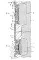
図1は、本発明の実施の形態1にかかる半導体集積回路装置の要部を示す縦断面図である。この半導体集積回路装置は、同一の半導体基板1上に、ディジタル回路を構成するディジタルCMOSトランジスタと、アナログ回路を構成するアナログCMOSトランジスタとが形成されたものである。ただし、図1では、それぞれディジタルNMOSトランジスタ101(同図左側)とアナログNMOSトランジスタ102(同図右側)が示されており、PMOSトランジスタについては省略している。
【0012】
ディジタルNMOSトランジスタ101は、P型の半導体基板1の一主面側に設けられたフィールド酸化膜2と、フィールド酸化膜2に囲まれた素子形成領域において半導体基板1の一主面側に設けられたPウェル領域3を備えている。Pウェル領域3において半導体基板1の一主面側には、表面濃度が5×10¹⁶〜2×10¹⁷/cm3程度のP-パンチスルーストッパー領域4が設けられている。このP-パンチスルーストッパー領域4において半導体基板1の一主面側には、N+ソース領域5、ソース側のN-LDD領域6、P-チャネル形成領域7、ドレイン側のN−LDD領域8およびN+ドレイン領域9が設けられている。
【0013】
また、P-チャネル形成領域7上にはゲート絶縁膜10を介してゲートポリシリコン11が形成されている。ゲートポリシリコン11の側部にはスペーサ酸化膜12が形成されている。ソース電極13、ゲート電極14およびドレイン電極15は、層間絶縁膜16に開口されたコンタクト穴を介して、それぞれN+ソース領域5、ゲートポリシリコン11およびN+ドレイン領域9に電気的に接続されている。さらにその上には、図示しない配線やパッシベーション膜などが積層される。
【0014】
上述した構成のディジタルNMOSトランジスタ101とともにディジタルCMOSトランジスタを構成するディジタルPMOSトランジスタは、半導体基板1の一主面側に設けられた図示しないNウェル領域において作製され、その構成はディジタルNMOSトランジスタ101と同様である。ただし、上述したディジタルNMOSトランジスタ101に関する説明の中で、半導体基板1を除いて、PをNに読み替え、またNをPに読み替える必要がある。
【0015】
上述した構成のディジタルCMOSトランジスタにおいては、たとえば最小チャネル長は0.6μm程度である。また、しきい値電圧は0.8V程度である。このディジタルCMOSトランジスタはロジック回路に使用される。
【0016】
アナログNMOSトランジスタ102は、P型の半導体基板1の一主面側に設けられたフィールド酸化膜22と、フィールド酸化膜22に囲まれた素子形成領域において半導体基板1の一主面側に設けられたPウェル領域23を備えている。Pウェル領域23において半導体基板1の一主面側には、N+ソース領域25、ソース側のN−LDD領域26、P-チャネル形成領域27、ドレイン側のN-LDD領域28およびN+ドレイン領域29が設けられている。
【0017】
また、P-チャネル形成領域27上にはゲート絶縁膜30を介してゲートポリシリコン31が形成されている。ゲートポリシリコン31の側部にはスペーサ酸化膜32が形成されている。ソース電極33、ゲート電極34およびドレイン電極35は、層間絶縁膜36に開口されたコンタクト穴を介してそれぞれN+ソース領域25、ゲートポリシリコン31およびN+ドレイン領域29に電気的に接続されている。さらにその上には、図示しない配線やパッシベーション膜などが積層される。
【0018】
上述した構成のアナログNMOSトランジスタ102とともにアナログCMOSトランジスタを構成するアナログPMOSトランジスタは、半導体基板1の一主面側に設けられた図示しないNウェル領域において作製され、その構成はアナログNMOSトランジスタ102と同様である。ただし、上述したアナログNMOSトランジスタ102に関する説明の中で、半導体基板1を除いて、PをNに読み替え、またNをPに読み替える必要がある。
【0019】
上述した構成のアナログCMOSトランジスタにおいては、たとえば最小チャネル長は1.0μm程度である。また、しきい値電圧はディジタルCMOSトランジスタよりも低く、0.6V程度である。このアナログCMOSトランジスタは、基準電圧回路、バイアス回路または各種オペアンプ回路など、しきい値電圧の高精度が要求される回路に使用される。そのため、ゲートポリシリコン31の加工バラツキなどをできるだけ抑制する必要があるので、ゲート長は4μm程度以上である。したがって、アナログCMOSトランジスタにおいては微細化は不要である。
【0020】
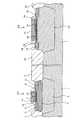
つぎに、実施の形態1にかかる半導体集積回路装置の製造プロセスについて説明する。図2および図3は、実施の形態1にかかる半導体集積回路装置の製造段階における要部を示す縦断面図である。まず、図2に示すように、半導体基板1の一主面側にPウェル領域3,23、フィールド酸化膜2,22およびゲート絶縁膜10,30をそれぞれ公知の方法により形成する。
【0021】
つづいて、アナログNMOSトランジスタ102の形成領域を被覆し、かつディジタルNMOSトランジスタ101の形成領域に対応する窓のパターンを有するマスク(図示せず)を用いて、イオン注入法によりディジタルNMOSトランジスタ101の形成領域にのみP-パンチスルーストッパー領域4を形成する。さらに、イオン注入法によりP-チャネル形成領域7,27を形成する。ここまでの状態が図2に示されている。
【0022】
つづいて、図3に示すように、ゲートポリシリコン11,31を形成し、これらゲートポリシリコン11,31をマスクとしたセルフアラインにて、イオン注入法によりN−LDD領域6,8,26,28を形成する。つづいて、ゲートポリシリコン11,31のそれぞれの側部にスペーサ酸化膜12,32を形成し、これらスペーサ酸化膜12,32をそれぞれマスクとしたセルフアラインにて、イオン注入法によりN+ソース領域5,25およびN+ドレイン領域9,29を形成する。なお、P-パンチスルーストッパー領域4を含む各不純物拡散領域は熱処理により活性化される。ここまでの状態が図3に示されている。
【0023】
つづいて、層間絶縁膜16(層間絶縁膜36と同じ)を積層し、コンタクト穴を開口する。そして、ソース電極13,33、ゲート電極14,34およびドレイン電極15,35をそれぞれパターニングして形成し、図1に示す状態となる。さらにその上に配線およびパッシベーション膜などを形成し、半導体集積回路装置ができあがる。なお、PMOSトランジスタも同様にして製造される。
【0024】
上述した実施の形態1によれば、同一の半導体基板1上に、パンチスルーストッパー領域4を備えたディジタルNMOSトランジスタ101と、パンチスルーストッパー領域のないアナログNMOSトランジスタ102とが形成されるので、アナログNMOSトランジスタ102においてバラツキ要因となる拡散層を1層減らすことができる。したがって、アナログNMOSトランジスタ102のしきい値電圧の精度低下を防ぐことができる。また、アナログNMOSトランジスタ102のしきい値電圧を低く設定することができる。ディジタルPMOSトランジスタおよびアナログPMOSトランジスタにおいても同様である。
【0025】
実施の形態2.
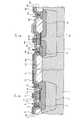
図4は、本発明の実施の形態2にかかる半導体集積回路装置の要部を示す縦断面図である。この半導体集積回路装置は、同一の半導体基板1上に、ディジタルCMOSトランジスタを構成するディジタルNMOSトランジスタ111(同図左側)およびディジタルPMOSトランジスタ(図示省略)と、アナログCMOSトランジスタを構成するアナログNMOSトランジスタ102(同図右側)およびアナログPMOSトランジスタ(図示省略)とが形成されたものである。なお、実施の形態1と同じ構成については同一の符号を付してその説明を省略する。
【0026】
ディジタルNMOSトランジスタ111は、P型の半導体基板1の一主面側にフィールド酸化膜2、Pウェル領域3、P-パンチスルーストッパー領域41、N+ソース領域5、ソース側のN−LDD領域6、P-チャネル形成領域7、ドレイン側のN−LDD領域8、N+ドレイン領域9、ゲート絶縁膜10、ゲートポリシリコン11、スペーサ酸化膜12、層間絶縁膜16、ソース電極13、ゲート電極14、およびドレイン電極15を有する。
【0027】
P-パンチスルーストッパー領域41は、その表面濃度が5×10¹⁶〜2×10¹⁷/cm3程度で、かつN−LDD領域6,8を囲うポケット構造となっている。また、ディジタルPMOSトランジスタは、P型の半導体基板1の一主面側に設けられた図示しないNウェル領域において作製され、その構成はディジタルNMOSトランジスタ111の説明においてPとNを読み替えた構成となる。
【0028】
上述した構成のディジタルCMOSトランジスタにおいては、たとえば最小チャネル長は0.6μm程度である。また、しきい値電圧は0.8V程度である。このディジタルCMOSトランジスタはロジック回路に使用される。
【0029】
実施の形態1と同様に、アナログPMOSトランジスタは、半導体基板1の一主面側に設けられた図示しないNウェル領域において作製され、その構成は実施の形態1中のアナログNMOSトランジスタ102の説明においてPとNを読み替えた構成となる。
【0030】
つぎに、実施の形態2にかかる半導体集積回路装置の製造プロセスについて説明する。図5および図6は、実施の形態2にかかる半導体集積回路装置の製造段階における要部を示す縦断面図である。まず、図5に示すように、半導体基板1の一主面側にPウェル領域3,23、フィールド酸化膜2,22およびゲート絶縁膜10,30をそれぞれ公知の方法により形成する。
【0031】
つづいて、イオン注入法によりP-チャネル形成領域7,27を形成した後、ゲートポリシリコン11,31を形成する。そして、ディジタルNMOSトランジスタ111の形成領域にのみ、ゲートポリシリコン11をマスクとしたセルフアラインにて、イオン注入法によりポケット構造のP-パンチスルーストッパー領域41を形成する。その際、アナログNMOSトランジスタ102の形成領域に不純物が打ち込まれないようにマスクしておく。ここまでの状態が図5に示されている。
【0032】
つづいて、図6に示すように、ゲートポリシリコン11,31をマスクとしたセルフアラインにて、イオン注入法によりN−LDD領域6,8,26,28を形成し、以後、実施の形態1と同様にしてスペーサ酸化膜12,32、N+ソース領域5,25およびN+ドレイン領域9,29を形成する。P-パンチスルーストッパー領域41を含む各不純物拡散領域は熱処理により活性化される。ここまでの状態が図6に示されている。
【0033】
しかる後、実施の形態1と同様にして、層間絶縁膜16,36、ソース電極13,33、ゲート電極14,34およびドレイン電極15,35を形成し、図4に示す状態となる。さらにその上に配線およびパッシベーション膜などを形成し、半導体集積回路装置ができあがる。なお、PMOSトランジスタも同様にして製造される。
【0034】
上述した実施の形態2によれば、同一の半導体基板1上に、パンチスルーストッパー領域41を備えたディジタルNMOSトランジスタ111と、パンチスルーストッパー領域のないアナログNMOSトランジスタ102とが形成されるので、アナログNMOSトランジスタ102においてバラツキ要因となる拡散層を1層減らすことができる。したがって、アナログNMOSトランジスタ102のしきい値電圧の精度低下を防ぐことができる。また、アナログNMOSトランジスタ102のしきい値電圧を低く設定することができる。ディジタルPMOSトランジスタおよびアナログPMOSトランジスタにおいても同様である。
【0035】
実施の形態3.
図7は、本発明の実施の形態3にかかる半導体集積回路装置の要部を示す縦断面図である。この半導体集積回路装置は、同一の半導体基板1上に、ディジタル回路を構成するディジタルCMOSトランジスタと、高耐圧回路を構成する高耐圧CMOSトランジスタとが形成されたものである。ただし、図7では、それぞれディジタルNMOSトランジスタ101(同図左側)と高耐圧NMOSトランジスタ122(同図右側)が示されており、PMOSトランジスタについては省略している。なお、実施の形態1と同じ構成については同一の符号を付して説明を省略する。
【0036】
高耐圧NMOSトランジスタ122は、P型の半導体基板1の一主面側に設けられたフィールド酸化膜52と、フィールド酸化膜52に囲まれた素子形成領域において半導体基板1の一主面側に設けられたPウェル領域53を備えている。Pウェル領域53において半導体基板1の一主面側には、N+ソース領域55、ソース側のN-LDD領域56、P-チャネル形成領域57およびN-オフセットドレイン領域67が設けられている。N-オフセットドレイン領域67において半導体基板1の一主面側には、選択酸化(LOCOS)領域68によりP-チャネル形成領域57から隔絶されたN+ドレイン領域59が設けられている。
【0037】
また、P-チャネル形成領域57上にはゲート絶縁膜60を介してゲートポリシリコン61が形成されている。ゲートポリシリコン61の側部にはスペーサ酸化膜62が形成されている。ソース電極63、ゲート電極64およびドレイン電極65は、層間絶縁膜66に開口されたコンタクト穴を介してそれぞれN+ソース領域55、ゲートポリシリコン61およびN+ドレイン領域59に電気的に接続されている。さらにその上には、図示しない配線やパッシベーション膜などが積層される。
【0038】
上述した構成の高耐圧NMOSトランジスタ122とともに高耐圧CMOSトランジスタを構成する高耐圧PMOSトランジスタは、半導体基板1の一主面側に設けられた図示しないNウェル領域において作製され、その構成は高耐圧NMOSトランジスタ122と同様である。ただし、上述した高耐圧NMOSトランジスタ122に関する説明の中で、半導体基板1を除いて、PをNに読み替え、またNをPに読み替える必要がある。
【0039】
上述した構成の高耐圧CMOSトランジスタにおいては、その不純物濃度およびxjは、要求される耐圧に応じて決まる。たとえば、耐圧が30V〜60Vクラスでは、xjは1μm程度であり、表面濃度は1×10¹⁷/cm3程度である。
【0040】
実施の形態1と同様に、ディジタルPMOSトランジスタは、半導体基板1の一主面側に設けられた図示しないNウェル領域において作製され、その構成は実施の形態1中のディジタルNMOSトランジスタ101の説明においてPとNを読み替えた構成となる。
【0041】
つぎに、実施の形態3にかかる半導体集積回路装置の製造プロセスについて説明する。図8および図9は、実施の形態3にかかる半導体集積回路装置の製造段階における要部を示す縦断面図である。まず、図8に示すように、半導体基板1の一主面側にPウェル領域3,53、N-オフセットドレイン領域67、フィールド酸化膜2,52と選択酸化(LOCOS)領域68、およびゲート絶縁膜10,60をそれぞれ公知の方法により形成する。
【0042】
つづいて、高耐圧NMOSトランジスタ122の形成領域を被覆し、かつディジタルNMOSトランジスタ101の形成領域に対応する窓のパターンを有するマスク(図示せず)を用いて、イオン注入法によりディジタルNMOSトランジスタ101の形成領域にのみP-パンチスルーストッパー領域4を形成する。さらに、イオン注入法によりP-チャネル形成領域7,57を形成する。ここまでの状態が図8に示されている。
【0043】
つづいて、図9に示すように、ゲートポリシリコン11,61を形成し、これらゲートポリシリコン11,61をマスクとしたセルフアラインにて、イオン注入法によりN−LDD領域6,8,56を形成する。つづいて、ゲートポリシリコン11,61のそれぞれの側部にスペーサ酸化膜12,62を形成し、これらスペーサ酸化膜12,62をそれぞれマスクとしたセルフアラインにて、イオン注入法によりN+ソース領域5,55およびN+ドレイン領域9を形成する。
【0044】
このとき、N+ドレイン領域59の形成領域にもイオン注入がおこなわれ、それによってN+ドレイン領域59が形成される。なお、P-パンチスルーストッパー領域4を含む各不純物拡散領域は熱処理により活性化される。ここまでの状態が図9に示されている。
【0045】
つづいて、層間絶縁膜16(層間絶縁膜66と同じ)を積層し、それにコンタクト穴を開口して、ソース電極13,63、ゲート電極14,64およびドレイン電極15,65を形成し、図7に示す状態となる。さらにその上に配線およびパッシベーション膜などを形成し、半導体集積回路装置ができあがる。なお、PMOSトランジスタも同様にして製造される。
【0046】
上述した実施の形態3によれば、同一の半導体基板1上に、パンチスルーストッパー領域4を備えたディジタルNMOSトランジスタ101と、パンチスルーストッパー領域のない高耐圧NMOSトランジスタ122とが形成されるので、高耐圧NMOSトランジスタ122の耐圧の低下を防ぐことができる。ディジタルPMOSトランジスタおよび高耐圧PMOSトランジスタにおいても同様である。
【0047】
なお、実施の形態3において、ディジタルNMOSトランジスタ101のパンチスルーストッパー領域4を、実施の形態2と同様に、ゲートポリシリコン11をマスクとしたセルフアラインで形成し、ポケット構造とすることもできる。
【0048】
実施の形態4.
図10は、本発明の実施の形態4にかかる半導体集積回路装置の要部を示す縦断面図である。この半導体集積回路装置は、同一の半導体基板1上に、ディジタル回路を構成するディジタルCMOSトランジスタと、高耐圧回路を構成する高耐圧CMOSトランジスタとが形成されたものである。
【0049】
ただし、図10では、それぞれディジタルNMOSトランジスタ101(同図左側)と高耐圧NMOSトランジスタ132(同図右側)が示されており、PMOSトランジスタについては省略している。なお、実施の形態1と同じ構成については同一の符号を付して説明を省略する。
【0050】
高耐圧NMOSトランジスタ132は、実施の形態3にかかる半導体集積回路装置の高耐圧NMOSトランジスタ122のソース部にP-パンチスルーストッパー領域71を追加した構成となっている。したがって、実施の形態3と同じ構成については同一の符号を付して説明を省略する。P-パンチスルーストッパー領域71は、Pウェル領域53において半導体基板1の一主面側で、かつN+ソース領域55およびソース側のN−LDD領域56を囲うように形成されている。
【0051】
上述した構成の高耐圧NMOSトランジスタ132とともに高耐圧CMOSトランジスタを構成する高耐圧PMOSトランジスタは、半導体基板1の一主面側に設けられた図示しないNウェル領域において作製され、その構成は高耐圧NMOSトランジスタ132と同様である。ただし、上述した高耐圧NMOSトランジスタ132に関する説明の中で、半導体基板1を除いて、PをNに読み替え、またNをPに読み替える必要がある。
【0052】
上述した構成の高耐圧CMOSトランジスタの不純物濃度およびxjは、要求される耐圧に応じて決まるが、たとえば、耐圧が30V〜60Vクラスでは、xjは1μm程度であり、表面濃度は1×10¹⁷/cm3程度である。
【0053】
実施の形態1と同様に、ディジタルPMOSトランジスタは、半導体基板1の一主面側に設けられた図示しないNウェル領域において作製され、その構成は実施の形態1中のディジタルNMOSトランジスタ101の説明においてPとNを読み替えた構成となる。
【0054】
つぎに、実施の形態4にかかる半導体集積回路装置の製造プロセスについて説明する。図11および図12は、実施の形態4にかかる半導体集積回路装置の製造段階における要部を示す縦断面図である。まず、図11に示すように、半導体基板1の一主面側にPウェル領域3,53、N-オフセットドレイン領域67、フィールド酸化膜2,52と選択酸化(LOCOS)領域68、およびゲート絶縁膜10,60をそれぞれ公知の方法により形成する。
【0055】
つづいて、高耐圧NMOSトランジスタ132のドレイン形成領域を被覆し、かつ高耐圧NMOSトランジスタ132のソース形成領域とディジタルNMOSトランジスタ101の形成領域に対応する窓のパターンを有するマスク(図示せず)を用いて、イオン注入法により、高耐圧NMOSトランジスタ132のソース形成領域にP-パンチスルーストッパー領域71を形成するとともに、ディジタルNMOSトランジスタ101の形成領域にP-パンチスルーストッパー領域4を形成する。さらに、イオン注入法によりP-チャネル形成領域7,57を形成する。ここまでの状態が図11に示されている。
【0056】
つづいて、図12に示すように、ゲートポリシリコン11,61を形成し、これらゲートポリシリコン11,61をマスクとしたセルフアラインにて、イオン注入法によりN-LDD領域6,8,56を形成する。つづいて、ゲートポリシリコン11,61のそれぞれの側部にスペーサ酸化膜12,62を形成し、これらスペーサ酸化膜12,62をそれぞれマスクとしたセルフアラインにて、イオン注入法によりN+ソース領域5,55およびN+ドレイン領域9を形成する。
【0057】
このとき、N+ドレイン領域59の形成領域にもイオン注入がおこなわれ、それによってN+ドレイン領域59が形成される。なお、P-パンチスルーストッパー領域4,71を含む各不純物拡散領域は熱処理により活性化される。ここまでの状態が図12に示されている。
【0058】
つづいて、層間絶縁膜16(層間絶縁膜66と同じ)を積層し、それにコンタクト穴を開口して、ソース電極13,63、ゲート電極14,64およびドレイン電極15,65を形成し、図10に示す状態となる。さらにその上に配線およびパッシベーション膜などを形成し、半導体集積回路装置ができあがる。なお、PMOSトランジスタも同様にして製造される。
【0059】
上述した実施の形態4によれば、同一の半導体基板1上に、パンチスルーストッパー領域4を備えたディジタルNMOSトランジスタ101と、ドレイン部にパンチスルーストッパー領域がなく、かつソース部にパンチスルーストッパー領域71を有する高耐圧NMOSトランジスタ132とが形成されるので、高耐圧NMOSトランジスタ132の耐圧の低下を防ぐことができるのに加えて、高耐圧NMOSトランジスタ132のチャネル長をより短くする、すなわち微細化することができる。ディジタルPMOSトランジスタおよび高耐圧PMOSトランジスタにおいても同様である。
【0060】
なお、実施の形態4において、ディジタルNMOSトランジスタ101のパンチスルーストッパー領域4を、実施の形態2と同様に、ゲートポリシリコン11をマスクとしたセルフアラインで形成し、ポケット構造とすることもできる。
【0061】
以上において本発明は、ディジタルCMOSトランジスタと、アナログCMOSトランジスタまたは高耐圧CMOSトランジスタとを同一基板上に集積する場合に限らず、ディジタルCMOSトランジスタおよびアナログCMOSトランジスタとバイポーラトランジスタとを集積する場合にも適用可能である。この場合には、たとえば図13に示すように、ウェル領域83をバイポーラトランジスタ201のコレクタ領域とし、ウェル領域83内の、ウェル領域83と反対の導電型の半導体領域87をベース領域とし、さらにそのベース領域となる半導体領域87内のソース・ドレイン領域に該当する半導体領域89をエミッタ領域とすればよい。たとえばnpnトランジスタの場合には、ウェル領域83はN型、ベース領域となる半導体領域87はP型、エミッタ領域となる半導体領域89はN型となる。そして、パンチスルーストッパー領域はディジタルCMOSトランジスタにのみ設けられる。ベース領域となる半導体領域87は、たとえば実施の形態3においてオフセットドレイン67を形成する際に同時形成される。なお、図13において、符号82は選択酸化領域、符号84および符号85はコンタクト用の高濃度不純物領域、符号86は層間絶縁膜、符号90はコレクタ電極、符号91はベース電極、符号92はエミッタ電極である。
【0062】
また、本発明は、ディジタルCMOSトランジスタおよびアナログCMOSトランジスタとダイオードとを集積する場合にも適用可能である。この場合には、たとえば図13に示す構成において、ウェル領域83とベース領域となる半導体領域87とのPN接合、あるいはベース領域となる半導体領域87とエミッタ領域となる半導体領域89とのPN接合を用いてダイオードを構成し、ディジタルCMOSトランジスタにのみパンチスルーストッパー領域を設ければよい。
【0063】
さらには、ディジタルCMOSトランジスタおよびアナログCMOSトランジスタと拡散抵抗とを集積する場合にも適用可能である。この場合には、たとえば図14に示すように、ウェル領域93上に形成した不純物拡散領域97を利用して拡散抵抗211を構成し、ディジタルCMOSトランジスタにのみパンチスルーストッパー領域を設ければよい。この不純物拡散領域97は、たとえば実施の形態3においてオフセットドレイン67を形成する際に同時形成される。ここで、拡散抵抗211は、たとえばxjが0.5〜2.5μm程度であり、表面の不純物濃度が1×10¹⁶〜5×10¹⁸/cm3程度である。なお、図14において、符号94は選択酸化領域、符号95はコンタクト用の高濃度不純物領域、符号96は層間絶縁膜、符号98は電極である。
【0064】
【発明の効果】
本発明によれば、同一の半導体基板上に、パンチスルーストッパー領域を備えたサブミクロンCMOSトランジスタと、パンチスルーストッパー領域のないアナログCMOSトランジスタ、高耐圧MOSトランジスタ、バイポーラトランジスタ、ダイオードまたは拡散抵抗とが形成されるので、それぞれの特性を劣化させることなく、サブミクロンCMOSトランジスタを、アナログCMOSトランジスタ、高耐圧MOSトランジスタ、バイポーラトランジスタ、ダイオードまたは拡散抵抗などと一緒に混載した半導体集積回路装置が得られるという効果を奏する。
【図面の簡単な説明】
【図1】本発明の実施の形態1にかかる半導体集積回路装置の要部を示す縦断面図である。
【図2】本発明の実施の形態1にかかる半導体集積回路装置の製造段階における要部を示す縦断面図である。
【図3】本発明の実施の形態1にかかる半導体集積回路装置の製造段階における要部を示す縦断面図である。
【図4】本発明の実施の形態2にかかる半導体集積回路装置の要部を示す縦断面図である。
【図5】本発明の実施の形態2にかかる半導体集積回路装置の製造段階における要部を示す縦断面図である。
【図6】本発明の実施の形態2にかかる半導体集積回路装置の製造段階における要部を示す縦断面図である。
【図7】本発明の実施の形態3にかかる半導体集積回路装置の要部を示す縦断面図である。
【図8】本発明の実施の形態3にかかる半導体集積回路装置の製造段階における要部を示す縦断面図である。
【図9】本発明の実施の形態3にかかる半導体集積回路装置の製造段階における要部を示す縦断面図である。
【図10】本発明の実施の形態4にかかる半導体集積回路装置の要部を示す縦断面図である。
【図11】本発明の実施の形態4にかかる半導体集積回路装置の製造段階における要部を示す縦断面図である。
【図12】本発明の実施の形態4にかかる半導体集積回路装置の製造段階における要部を示す縦断面図である。
【図13】本発明にかかる半導体集積回路装置においてバイポーラトランジスタが集積された部分の要部を示す縦断面図である。
【図14】本発明にかかる半導体集積回路装置において拡散抵抗が集積された部分の要部を示す縦断面図である。
【符号の説明】
1 半導体基板
4,41,71 パンチスルーストッパー領域
5,55 ソース領域
9,59 ドレイン領域
67 オフセットドレイン領域
101,111 ディジタルNMOSトランジスタ(第1のMOSトランジスタ)
102 アナログNMOSトランジスタ(第2のMOSトランジスタ)
122,132 高耐圧NMOSトランジスタ
201 バイポーラトランジスタ
211 拡散抵抗[0001]
BACKGROUND OF THE INVENTION
The present invention relates to a semiconductor integrated circuit device and a manufacturing method thereof, and more particularly to a semiconductor integrated circuit device suitable for application to a power IC in which a digital circuit, an analog circuit, and a high voltage circuit are mounted together.
[0002]
[Prior art]
Conventionally, a logic circuit mounted on a power IC is small-scale, and a miniaturization process such as a memory or a logic LSI is unnecessary. However, in recent years, in the field of power management for power ICs and the like, with the high performance of voltage monitoring and charging functions, it is necessary to perform self-correction by a CPU or the like. Therefore, it is necessary to mount a large-scale logic circuit on the power IC.
[0003]
In general, in a memory, logic LSI, or the like, a submicron MOS transistor having a channel length shorter than 1 μm is used for high integration. In such a short channel type MOS transistor, a punch-through stopper layer is provided in order to suppress punch-through between the source region and the drain region. A semiconductor integrated circuit device having a punch-through stopper layer is described in Japanese Patent Application Laid-Open No. 61-199093.
[0004]
Japanese Patent Application Laid-Open No. 60-10780 describes a method of forming a punch-through stopper layer by an ion implantation method. Japanese Patent Application Laid-Open No. 60-105277 describes a method of manufacturing a MOS transistor employing an LDD structure with a P pocket in order to alleviate electric field concentration near the drain region.
[0005]
[Problems to be solved by the invention]
However, when the above-described submicron MOS transistor having the punch-through stopper layer is integrated on the same substrate together with an analog CMOS transistor, a high voltage MOS transistor, a bipolar transistor, a diode, a diffusion resistor, etc., an analog CMOS transistor, a high If a punch-through stopper layer is also formed in a high-voltage MOS transistor, bipolar transistor, diode, and diffusion resistor, the threshold voltage accuracy of the analog CMOS transistor is reduced due to variations in the surface concentration of the diffusion layer. There is a problem that the breakdown voltage of the high breakdown voltage MOS transistor is lowered.
[0006]
The present invention has been made in view of the above problems, and submicron CMOS transistors, together with analog CMOS transistors, high-voltage MOS transistors, bipolar transistors, diodes, diffused resistors, and the like, deteriorate their characteristics. An object of the present invention is to provide a semiconductor integrated circuit device mixedly mounted on the same substrate.
[0007]
Another object of the present invention is to mount a submicron CMOS transistor, an analog CMOS transistor, a high voltage MOS transistor, a bipolar transistor, a diode or a diffused resistor on the same substrate without degrading the respective characteristics. It is an object of the present invention to provide a method of manufacturing a semiconductor integrated circuit device capable of performing the above.
[0008]
[Means for Solving the Problems]
In order to achieve the above object, a semiconductor integrated circuit device according to the present invention has an analog CMOS transistor, a high voltage MOS transistor, a bipolar transistor, a diode or a diffusion when a punch-through stopper layer is formed on one main surface side of a semiconductor substrate. By masking the region for forming the resistor and exposing the region for forming the submicron CMOS transistor, for example, by ion implantation, the region for forming the analog CMOS transistor, high voltage MOS transistor, bipolar transistor, diode or diffused resistor is formed. Prevent formation of punch-through stopper region.
[0009]
According to the present invention, a submicron CMOS transistor having a punch-through stopper region, an analog CMOS transistor without a punch-through stopper region, a high voltage MOS transistor, a bipolar transistor, a diode or a diffused resistor on the same semiconductor substrate. It is formed.
[0010]
DETAILED DESCRIPTION OF THE INVENTION
Hereinafter, a semiconductor integrated circuit device according to an embodiment of the present invention will be described in detail with reference to the drawings.
[0011]
FIG. 1 is a longitudinal sectional view showing a main part of the semiconductor integrated circuit device according to the first embodiment of the present invention. In this semiconductor integrated circuit device, a digital CMOS transistor constituting a digital circuit and an analog CMOS transistor constituting an analog circuit are formed on the
[0012]
The
[0013]
P- A
[0014]
The digital PMOS transistor that constitutes the digital CMOS transistor together with the
[0015]
In the digital CMOS transistor having the above-described configuration, for example, the minimum channel length is about 0.6 μm. The threshold voltage is about 0.8V. This digital CMOS transistor is used in a logic circuit.
[0016]
The
[0017]
P-
[0018]
The analog PMOS transistor that constitutes the analog CMOS transistor together with the
[0019]
In the analog CMOS transistor having the above-described configuration, for example, the minimum channel length is about 1.0 μm. The threshold voltage is lower than that of the digital CMOS transistor and is about 0.6V. This analog CMOS transistor is used in a circuit that requires high accuracy of a threshold voltage, such as a reference voltage circuit, a bias circuit, or various operational amplifier circuits. For this reason, since it is necessary to suppress processing variations of the
[0020]
Next, a manufacturing process of the semiconductor integrated circuit device according to the first embodiment will be described. 2 and FIG. 3 are longitudinal sectional views showing main parts in the manufacturing stage of the semiconductor integrated circuit device according to the first embodiment. First, as shown in FIG. 2, P well
[0021]
Subsequently, the
[0022]
Subsequently, as shown in FIG. 3, gate polysilicons 11 and 31 are formed, and N-
[0023]
Subsequently, an interlayer insulating film 16 (same as the interlayer insulating film 36) is laminated, and a contact hole is opened. Then, the
[0024]
According to the first embodiment described above, since the
[0025]
FIG. 4 is a longitudinal sectional view showing a main part of the semiconductor integrated circuit device according to the second embodiment of the present invention. In this semiconductor integrated circuit device, a digital NMOS transistor 111 (left side in the figure) and a digital PMOS transistor (not shown) constituting a digital CMOS transistor and an
[0026]
The
[0027]
P- The punch-through
[0028]
In the digital CMOS transistor having the above-described configuration, for example, the minimum channel length is about 0.6 μm. The threshold voltage is about 0.8V. This digital CMOS transistor is used in a logic circuit.
[0029]
Similar to the first embodiment, the analog PMOS transistor is manufactured in an N well region (not shown) provided on one main surface side of the
[0030]
Next, a manufacturing process of the semiconductor integrated circuit device according to the second embodiment will be described. FIGS. 5 and 6 are longitudinal sectional views showing main parts in the manufacturing stage of the semiconductor integrated circuit device according to the second embodiment. First, as shown in FIG. 5, P well
[0031]
Subsequently, P is ion-implanted.- After the
[0032]
Subsequently, as shown in FIG. 6, N-
[0033]
Thereafter, in the same manner as in the first embodiment,
[0034]
According to the second embodiment described above, the
[0035]
FIG. 7 is a longitudinal sectional view showing a main part of the semiconductor integrated circuit device according to the third embodiment of the present invention. In this semiconductor integrated circuit device, a digital CMOS transistor constituting a digital circuit and a high voltage CMOS transistor constituting a high voltage circuit are formed on the
[0036]
The high breakdown
[0037]
P-
[0038]
A high breakdown voltage PMOS transistor that forms a high breakdown voltage CMOS transistor together with the high breakdown
[0039]
In the high breakdown voltage CMOS transistor having the above-described configuration, the impurity concentration and xj are determined according to the required breakdown voltage. For example, when the breakdown voltage is 30V to 60V class, xj is about 1 μm and the surface concentration is 1 × 10.17 / CmThree Degree.
[0040]
Similar to the first embodiment, the digital PMOS transistor is manufactured in an N-well region (not shown) provided on one main surface side of the
[0041]
Next, a manufacturing process of the semiconductor integrated circuit device according to the third embodiment will be described. FIG. 8 and FIG. 9 are longitudinal sectional views showing main parts in the manufacturing stage of the semiconductor integrated circuit device according to the third embodiment. First, as shown in FIG. 8, P well
[0042]
Subsequently, by using a mask (not shown) that covers the formation region of the high breakdown
[0043]
Subsequently, as shown in FIG. 9, gate polysilicons 11 and 61 are formed, and N-
[0044]
At this time, N+ Ion implantation is also performed in the formation region of the
[0045]
Subsequently, an interlayer insulating film 16 (same as the interlayer insulating film 66) is laminated, contact holes are opened in the
[0046]
According to the above-described third embodiment, the
[0047]
In the third embodiment, the punch-through
[0048]
FIG. 10 is a longitudinal sectional view showing a main part of the semiconductor integrated circuit device according to the fourth embodiment of the present invention. In this semiconductor integrated circuit device, a digital CMOS transistor constituting a digital circuit and a high voltage CMOS transistor constituting a high voltage circuit are formed on the
[0049]
However, in FIG. 10, a digital NMOS transistor 101 (left side of the figure) and a high voltage NMOS transistor 132 (right side of the figure) are shown, and the PMOS transistor is omitted. In addition, about the same structure as
[0050]
The high
[0051]
A high breakdown voltage PMOS transistor that constitutes a high breakdown voltage CMOS transistor together with the high breakdown
[0052]
The impurity concentration and xj of the high breakdown voltage CMOS transistor having the above-described configuration are determined according to the required breakdown voltage. For example, when the breakdown voltage is 30V to 60V class, xj is about 1 μm and the surface concentration is 1 × 10.17 / CmThree Degree.
[0053]
Similar to the first embodiment, the digital PMOS transistor is manufactured in an N-well region (not shown) provided on one main surface side of the
[0054]
Next, a manufacturing process of the semiconductor integrated circuit device according to the fourth embodiment will be described. FIG. 11 and FIG. 12 are longitudinal sectional views showing main parts in the manufacturing stage of the semiconductor integrated circuit device according to the fourth embodiment. First, as shown in FIG. 11, P well
[0055]
Subsequently, a mask (not shown) that covers the drain formation region of the high breakdown
[0056]
Subsequently, as shown in FIG. 12, gate polysilicons 11 and 61 are formed, and N is formed by ion implantation by self-alignment using the gate polysilicons 11 and 61 as a mask.-
[0057]
At this time, N+ Ion implantation is also performed in the formation region of the
[0058]
Subsequently, an interlayer insulating film 16 (same as the interlayer insulating film 66) is stacked, contact holes are opened in the
[0059]
According to the fourth embodiment described above, the
[0060]
In the fourth embodiment, the punch-through
[0061]
As described above, the present invention is not limited to the case where the digital CMOS transistor and the analog CMOS transistor or the high voltage CMOS transistor are integrated on the same substrate, but is also applied to the case where the digital CMOS transistor, the analog CMOS transistor and the bipolar transistor are integrated. Is possible. In this case, for example, as shown in FIG. 13, the
[0062]
The present invention is also applicable to the case where a digital CMOS transistor, an analog CMOS transistor and a diode are integrated. In this case, for example, in the configuration shown in FIG. 13, a PN junction between the
[0063]
Furthermore, the present invention can also be applied to the case where a digital CMOS transistor, an analog CMOS transistor and a diffusion resistor are integrated. In this case, for example, as shown in FIG. 14, a diffusion resistor 211 is formed using an
[0064]
【The invention's effect】
According to the present invention, a submicron CMOS transistor having a punch-through stopper region, an analog CMOS transistor without a punch-through stopper region, a high voltage MOS transistor, a bipolar transistor, a diode, or a diffused resistor on the same semiconductor substrate. Therefore, it is possible to obtain a semiconductor integrated circuit device in which a submicron CMOS transistor is mixedly mounted together with an analog CMOS transistor, a high voltage MOS transistor, a bipolar transistor, a diode, a diffused resistor, or the like without degrading the respective characteristics. There is an effect.
[Brief description of the drawings]
FIG. 1 is a longitudinal sectional view showing a main part of a semiconductor integrated circuit device according to a first embodiment of the present invention;
FIG. 2 is a longitudinal sectional view showing a main part in a manufacturing stage of the semiconductor integrated circuit device according to the first embodiment of the invention;
FIG. 3 is a longitudinal sectional view showing a main part in a manufacturing stage of the semiconductor integrated circuit device according to the first embodiment of the invention;
FIG. 4 is a longitudinal sectional view showing a main part of a semiconductor integrated circuit device according to a second embodiment of the present invention.
FIG. 5 is a longitudinal sectional view showing a main part in a manufacturing stage of a semiconductor integrated circuit device according to a second embodiment of the present invention;
FIG. 6 is a longitudinal sectional view showing a main part in a manufacturing stage of a semiconductor integrated circuit device according to a second embodiment of the present invention;
FIG. 7 is a longitudinal sectional view showing a main part of a semiconductor integrated circuit device according to a third embodiment of the present invention.
FIG. 8 is a longitudinal sectional view showing a main part in a manufacturing stage of a semiconductor integrated circuit device according to a third embodiment of the present invention;
FIG. 9 is a longitudinal sectional view showing a main part in a manufacturing stage of a semiconductor integrated circuit device according to a third embodiment of the present invention;
FIG. 10 is a longitudinal sectional view showing a main part of a semiconductor integrated circuit device according to a fourth embodiment of the present invention.
FIG. 11 is a longitudinal sectional view showing a main part in a manufacturing stage of a semiconductor integrated circuit device according to a fourth embodiment of the present invention;
FIG. 12 is a longitudinal sectional view showing a main part of a semiconductor integrated circuit device according to a fourth embodiment of the present invention at the manufacturing stage.
FIG. 13 is a longitudinal sectional view showing a main part of a portion where bipolar transistors are integrated in the semiconductor integrated circuit device according to the present invention.
FIG. 14 is a longitudinal sectional view showing a main part of a portion where diffused resistors are integrated in the semiconductor integrated circuit device according to the present invention.
[Explanation of symbols]
1 Semiconductor substrate
4, 41, 71 Punch-through stopper area
5,55 source region
9,59 drain region
67 Offset drain region
101,111 Digital NMOS transistor (first MOS transistor)
102 Analog NMOS transistor (second MOS transistor)
122,132 High voltage NMOS transistor
201 Bipolar Transistor
211 Diffusion resistance
Claims (4)
Translated fromJapanese前記第1のMOSトランジスタのゲート電極となるゲートポリシリコンを形成した後、前記半導体素子をマスクしながら、前記ゲートポリシリコンをマスクとしたセルフアラインによるイオン注入法により、前記第1のMOSトランジスタの形成領域の一部に前記パンチスルーストッパー領域を形成し、当該パンチスルーストッパー領域内にソース領域およびドレイン領域が形成されることを特徴とする半導体集積回路装置の製造方法。A first MOS transistor, a second MOS transistor, and a high voltage MOS transistor are integrated on the same semiconductor substrate, and the second MOS transistor has a threshold voltage lower than that of the first MOS transistor, The first MOS transistor has a shorter channel length than the second MOS transistor and surrounds the first MOS transistor so as to cover at least the regions below the source region and the drain region of the first MOS transistor. A punch-through stopper region having a pocket structure for ensuring a punch-through breakdown voltage between the drain region and the high-breakdown-voltage MOS transistor further includes a drain region having an offset drain region whose impurity concentration is lower than that of the drain region. Surrounded by the area below the area, One Uponleast in the offset drain region to produce a semiconductor integrated circuit devicewhich is not provided with the punch-through stopper area provided on the first MOS transistor,
After forming the gate polysilicon as a gate electrode of saidfirst MOS transistor, wherein while the semiconductor element is masked, by ion implantation by the self-alignment as a mask the gate polysilicon, thefirst MOS transistor A method of manufacturing a semiconductor integrated circuit device, wherein the punch-through stopper region is formed in a part of a formation region, and a source region and a drain region are formed in the punch-through stopper region.
Priority Applications (5)
| Application Number | Priority Date | Filing Date | Title |
|---|---|---|---|
| JP2001015042AJP4765014B2 (en) | 2001-01-23 | 2001-01-23 | Semiconductor integrated circuit device and manufacturing method thereof |
| EP02250304AEP1225626B1 (en) | 2001-01-23 | 2002-01-16 | Semiconductor integrated circuit device and manufacture method therefor |
| DE60232474TDE60232474D1 (en) | 2001-01-23 | 2002-01-16 | Integrated semiconductor circuit and associated manufacturing method |
| US10/055,722US6833594B2 (en) | 2001-01-23 | 2002-01-23 | Semiconductor integrated circuit device and manufacture method therefore |
| US10/869,811US7138311B2 (en) | 2001-01-23 | 2004-06-16 | Semiconductor integrated circuit device and manufacture method therefore |
Applications Claiming Priority (1)
| Application Number | Priority Date | Filing Date | Title |
|---|---|---|---|
| JP2001015042AJP4765014B2 (en) | 2001-01-23 | 2001-01-23 | Semiconductor integrated circuit device and manufacturing method thereof |
Publications (2)
| Publication Number | Publication Date |
|---|---|
| JP2002222867A JP2002222867A (en) | 2002-08-09 |
| JP4765014B2true JP4765014B2 (en) | 2011-09-07 |
Family
ID=18881658
Family Applications (1)
| Application Number | Title | Priority Date | Filing Date |
|---|---|---|---|
| JP2001015042AExpired - Fee RelatedJP4765014B2 (en) | 2001-01-23 | 2001-01-23 | Semiconductor integrated circuit device and manufacturing method thereof |
Country Status (4)
| Country | Link |
|---|---|
| US (2) | US6833594B2 (en) |
| EP (1) | EP1225626B1 (en) |
| JP (1) | JP4765014B2 (en) |
| DE (1) | DE60232474D1 (en) |
Families Citing this family (8)
| Publication number | Priority date | Publication date | Assignee | Title |
|---|---|---|---|---|
| KR100582374B1 (en)* | 2004-09-08 | 2006-05-22 | 매그나칩 반도체 유한회사 | High voltage transistor and method of manufacturing the same |
| US9159568B2 (en)* | 2006-02-04 | 2015-10-13 | Cypress Semiconductor Corporation | Method for fabricating memory cells having split charge storage nodes |
| US8866263B2 (en)* | 2006-09-26 | 2014-10-21 | Texas Instruments Incorporated | Emitter ballasting by contact area segmentation in ESD bipolar based semiconductor component |
| JP5332781B2 (en)* | 2009-03-19 | 2013-11-06 | 富士通セミコンダクター株式会社 | Manufacturing method of semiconductor device |
| JP5330899B2 (en)* | 2009-05-25 | 2013-10-30 | 株式会社東芝 | Semiconductor device and manufacturing method thereof |
| JP2011096862A (en)* | 2009-10-30 | 2011-05-12 | Hitachi Ltd | Semiconductor device and method of manufacturing the same |
| JP5648413B2 (en)* | 2009-11-09 | 2015-01-07 | 東芝ライテック株式会社 | Lighting device |
| TW202427797A (en) | 2022-12-28 | 2024-07-01 | 聯華電子股份有限公司 | High-voltage transistor, level-up shifting circuit, and semiconductor device |
Family Cites Families (33)
| Publication number | Priority date | Publication date | Assignee | Title |
|---|---|---|---|---|
| US4403395A (en)* | 1979-02-15 | 1983-09-13 | Texas Instruments Incorporated | Monolithic integration of logic, control and high voltage interface circuitry |
| JPS6010780A (en) | 1983-06-30 | 1985-01-19 | Fujitsu Ltd | Manufacture of semiconductor device |
| JPS60105277A (en) | 1983-11-11 | 1985-06-10 | Toshiba Corp | MOS transistor manufacturing method |
| JPS6114744A (en)* | 1984-06-29 | 1986-01-22 | Fujitsu Ltd | semiconductor equipment |
| JPS6167252A (en)* | 1984-09-10 | 1986-04-07 | Nec Corp | semiconductor equipment |
| JPS61190983A (en) | 1985-02-20 | 1986-08-25 | Hitachi Ltd | Semiconductor integrated circuit device |
| JPS6220416A (en)* | 1985-07-19 | 1987-01-29 | Hitachi Ltd | Semiconductor integrated circuit |
| JPH0199251A (en)* | 1987-10-13 | 1989-04-18 | Mitsubishi Electric Corp | Semiconductor integrated circuit device |
| JP2937338B2 (en)* | 1989-02-10 | 1999-08-23 | 株式会社東芝 | Semiconductor device |
| JP2545762B2 (en)* | 1990-04-13 | 1996-10-23 | 日本電装株式会社 | High breakdown voltage MIS transistor and method of manufacturing complementary transistor having this transistor |
| JPH04113669A (en)* | 1990-09-03 | 1992-04-15 | Nec Ic Microcomput Syst Ltd | Semiconductor device |
| US5559044A (en)* | 1992-09-21 | 1996-09-24 | Siliconix Incorporated | BiCDMOS process technology |
| JPH06295988A (en)* | 1993-02-09 | 1994-10-21 | Matsushita Electric Ind Co Ltd | Semiconductor device and manufacturing method thereof |
| JP3235277B2 (en)* | 1993-06-07 | 2001-12-04 | ソニー株式会社 | Method for manufacturing transistor |
| JPH0794734A (en)* | 1993-09-24 | 1995-04-07 | Sony Corp | Method of manufacturing transistor with high withstanding voltage |
| US5409848A (en)* | 1994-03-31 | 1995-04-25 | Vlsi Technology, Inc. | Angled lateral pocket implants on p-type semiconductor devices |
| JP3055424B2 (en)* | 1994-04-28 | 2000-06-26 | 株式会社デンソー | Method of manufacturing MIS type semiconductor device |
| JP3601612B2 (en)* | 1994-09-22 | 2004-12-15 | 富士通株式会社 | Semiconductor device and manufacturing method thereof |
| US5516711A (en)* | 1994-12-16 | 1996-05-14 | Mosel Vitelic, Inc. | Method for forming LDD CMOS with oblique implantation |
| US6127700A (en)* | 1995-09-12 | 2000-10-03 | National Semiconductor Corporation | Field-effect transistor having local threshold-adjust doping |
| JP3386101B2 (en)* | 1996-08-29 | 2003-03-17 | シャープ株式会社 | Method for manufacturing semiconductor device |
| US5830789A (en)* | 1996-11-19 | 1998-11-03 | Integrated Device Technology, Inc. | CMOS process forming wells after gate formation |
| US5899732A (en)* | 1997-04-11 | 1999-05-04 | Advanced Micro Devices, Inc. | Method of implanting silicon through a polysilicon gate for punchthrough control of a semiconductor device |
| US6096591A (en)* | 1997-06-30 | 2000-08-01 | Advanced Micro Devices, Inc. | Method of making an IGFET and a protected resistor with reduced processing steps |
| US6294416B1 (en)* | 1998-01-23 | 2001-09-25 | Texas Instruments-Acer Incorporated | Method of fabricating CMOS transistors with self-aligned planarization twin-well by using fewer mask counts |
| US5963799A (en)* | 1998-03-23 | 1999-10-05 | Texas Instruments - Acer Incorporated | Blanket well counter doping process for high speed/low power MOSFETs |
| US6157062A (en)* | 1998-04-13 | 2000-12-05 | Texas Instruments Incorporated | Integrating dual supply voltage by removing the drain extender implant from the high voltage device |
| JP3536693B2 (en)* | 1998-11-24 | 2004-06-14 | セイコーエプソン株式会社 | Semiconductor storage device and method of manufacturing the same |
| US6238982B1 (en)* | 1999-04-13 | 2001-05-29 | Advanced Micro Devices | Multiple threshold voltage semiconductor device fabrication technology |
| TW411509B (en)* | 1999-06-05 | 2000-11-11 | United Microelectronics Corp | Integrated manufacturing method of high voltage and low voltage device |
| JP3546783B2 (en)* | 1999-06-09 | 2004-07-28 | セイコーエプソン株式会社 | Semiconductor storage device and method of manufacturing the same |
| TW466704B (en)* | 1999-09-10 | 2001-12-01 | Koninkl Philips Electronics Nv | Integrated circuit |
| US6355531B1 (en)* | 2000-08-09 | 2002-03-12 | International Business Machines Corporation | Method for fabricating semiconductor devices with different properties using maskless process |
- 2001
- 2001-01-23JPJP2001015042Apatent/JP4765014B2/ennot_activeExpired - Fee Related
- 2002
- 2002-01-16EPEP02250304Apatent/EP1225626B1/ennot_activeExpired - Lifetime
- 2002-01-16DEDE60232474Tpatent/DE60232474D1/ennot_activeExpired - Lifetime
- 2002-01-23USUS10/055,722patent/US6833594B2/ennot_activeExpired - Lifetime
- 2004
- 2004-06-16USUS10/869,811patent/US7138311B2/ennot_activeExpired - Fee Related
Also Published As
| Publication number | Publication date |
|---|---|
| EP1225626B1 (en) | 2009-06-03 |
| DE60232474D1 (en) | 2009-07-16 |
| US7138311B2 (en) | 2006-11-21 |
| US6833594B2 (en) | 2004-12-21 |
| JP2002222867A (en) | 2002-08-09 |
| EP1225626A2 (en) | 2002-07-24 |
| US20040232498A1 (en) | 2004-11-25 |
| US20020117723A1 (en) | 2002-08-29 |
| EP1225626A3 (en) | 2005-01-12 |
Similar Documents
| Publication | Publication Date | Title |
|---|---|---|
| CN100517712C (en) | Semiconductor device with stable electrostatic discharge protection capability | |
| KR19980064498A (en) | Semiconductor device and manufacturing method thereof | |
| JP2004241613A (en) | Semiconductor device | |
| JP2000286346A (en) | Semiconductor device and manufacturing method thereof | |
| JP4765014B2 (en) | Semiconductor integrated circuit device and manufacturing method thereof | |
| CN102044494B (en) | Method for manufacturing semiconductor device | |
| JP4477197B2 (en) | Manufacturing method of semiconductor device | |
| JP3415401B2 (en) | Semiconductor integrated circuit device and method of manufacturing the same | |
| JPS58170047A (en) | Semiconductor device | |
| JP2882309B2 (en) | Input protection circuit and method of manufacturing semiconductor integrated circuit device | |
| JPH05102475A (en) | Semiconductor device and manufacturing method thereof | |
| JP3734413B2 (en) | MOS diode for electrostatic protection, input / output protection circuit, and semiconductor device including the same | |
| US20090159984A1 (en) | Semiconductor Device and Method for Manufacturing the Same | |
| JP3788439B2 (en) | Manufacturing method of semiconductor device | |
| JP2002222869A (en) | Semiconductor integrated circuit device and method of manufacturing the same | |
| JP3390336B2 (en) | Semiconductor integrated circuit device and method of manufacturing the same | |
| JPH10335485A (en) | Semiconductor device and manufacturing method thereof | |
| US5970349A (en) | Semiconductor device having one or more asymmetric background dopant regions and method of manufacture thereof | |
| JP2006185952A (en) | Semiconductor device and manufacturing method thereof | |
| JP2001156181A (en) | Semiconductor device | |
| JPH08321604A (en) | Method for manufacturing semiconductor device | |
| KR940006673B1 (en) | Semiconductor device and manufacturing method | |
| JPH09260644A (en) | Semiconductor device | |
| JPH0319709B2 (en) | ||
| JPH09199718A (en) | Semiconductor integrated circuit device and method of manufacturing the same |
Legal Events
| Date | Code | Title | Description |
|---|---|---|---|
| A621 | Written request for application examination | Free format text:JAPANESE INTERMEDIATE CODE: A621 Effective date:20070614 | |
| A711 | Notification of change in applicant | Free format text:JAPANESE INTERMEDIATE CODE: A712 Effective date:20091112 | |
| RD03 | Notification of appointment of power of attorney | Free format text:JAPANESE INTERMEDIATE CODE: A7423 Effective date:20091112 | |
| RD04 | Notification of resignation of power of attorney | Free format text:JAPANESE INTERMEDIATE CODE: A7424 Effective date:20091112 | |
| A977 | Report on retrieval | Free format text:JAPANESE INTERMEDIATE CODE: A971007 Effective date:20091202 | |
| A131 | Notification of reasons for refusal | Free format text:JAPANESE INTERMEDIATE CODE: A131 Effective date:20091222 | |
| A521 | Request for written amendment filed | Free format text:JAPANESE INTERMEDIATE CODE: A523 Effective date:20100222 | |
| A02 | Decision of refusal | Free format text:JAPANESE INTERMEDIATE CODE: A02 Effective date:20100713 | |
| A521 | Request for written amendment filed | Free format text:JAPANESE INTERMEDIATE CODE: A523 Effective date:20101008 | |
| A911 | Transfer to examiner for re-examination before appeal (zenchi) | Free format text:JAPANESE INTERMEDIATE CODE: A911 Effective date:20101018 | |
| TRDD | Decision of grant or rejection written | ||
| A01 | Written decision to grant a patent or to grant a registration (utility model) | Free format text:JAPANESE INTERMEDIATE CODE: A01 Effective date:20110419 | |
| A711 | Notification of change in applicant | Free format text:JAPANESE INTERMEDIATE CODE: A712 Effective date:20110422 | |
| A61 | First payment of annual fees (during grant procedure) | Free format text:JAPANESE INTERMEDIATE CODE: A61 Effective date:20110502 | |
| R150 | Certificate of patent or registration of utility model | Ref document number:4765014 Country of ref document:JP Free format text:JAPANESE INTERMEDIATE CODE: R150 Free format text:JAPANESE INTERMEDIATE CODE: R150 | |
| FPAY | Renewal fee payment (event date is renewal date of database) | Free format text:PAYMENT UNTIL: 20140624 Year of fee payment:3 | |
| R250 | Receipt of annual fees | Free format text:JAPANESE INTERMEDIATE CODE: R250 | |
| R250 | Receipt of annual fees | Free format text:JAPANESE INTERMEDIATE CODE: R250 | |
| R250 | Receipt of annual fees | Free format text:JAPANESE INTERMEDIATE CODE: R250 | |
| R250 | Receipt of annual fees | Free format text:JAPANESE INTERMEDIATE CODE: R250 | |
| R250 | Receipt of annual fees | Free format text:JAPANESE INTERMEDIATE CODE: R250 | |
| LAPS | Cancellation because of no payment of annual fees |