JP4763841B2 - Substrate processing apparatus and semiconductor device manufacturing method - Google Patents
Substrate processing apparatus and semiconductor device manufacturing methodDownload PDFInfo
- Publication number
- JP4763841B2 JP4763841B2JP2010140438AJP2010140438AJP4763841B2JP 4763841 B2JP4763841 B2JP 4763841B2JP 2010140438 AJP2010140438 AJP 2010140438AJP 2010140438 AJP2010140438 AJP 2010140438AJP 4763841 B2JP4763841 B2JP 4763841B2
- Authority
- JP
- Japan
- Prior art keywords
- chamber
- substrate
- transfer chamber
- transfer
- opening
- Prior art date
- Legal status (The legal status is an assumption and is not a legal conclusion. Google has not performed a legal analysis and makes no representation as to the accuracy of the status listed.)
- Expired - Fee Related
Links
- 239000000758substrateSubstances0.000titleclaimsdescription104
- 238000012545processingMethods0.000titleclaimsdescription96
- 238000004519manufacturing processMethods0.000titleclaimsdescription14
- 239000004065semiconductorSubstances0.000titleclaimsdescription8
- 238000012546transferMethods0.000claimsdescription179
- 238000000034methodMethods0.000claimsdescription23
- 238000004140cleaningMethods0.000claimsdescription9
- 238000010438heat treatmentMethods0.000claimsdescription6
- 238000010926purgeMethods0.000claimsdescription4
- 238000012423maintenanceMethods0.000description101
- 235000012431wafersNutrition0.000description81
- 239000007789gasSubstances0.000description15
- IJGRMHOSHXDMSA-UHFFFAOYSA-NAtomic nitrogenChemical compoundN#NIJGRMHOSHXDMSA-UHFFFAOYSA-N0.000description9
- 229910001873dinitrogenInorganic materials0.000description8
- 238000009434installationMethods0.000description6
- 238000013459approachMethods0.000description3
- 230000000694effectsEffects0.000description3
- VYPSYNLAJGMNEJ-UHFFFAOYSA-NSilicium dioxideChemical compoundO=[Si]=OVYPSYNLAJGMNEJ-UHFFFAOYSA-N0.000description2
- 230000006837decompressionEffects0.000description2
- 230000007423decreaseEffects0.000description2
- 239000002184metalSubstances0.000description2
- 239000002245particleSubstances0.000description2
- 238000013404process transferMethods0.000description2
- QVGXLLKOCUKJST-UHFFFAOYSA-Natomic oxygenChemical compound[O]QVGXLLKOCUKJST-UHFFFAOYSA-N0.000description1
- 230000015572biosynthetic processEffects0.000description1
- 238000007664blowingMethods0.000description1
- 239000000919ceramicSubstances0.000description1
- 230000003749cleanlinessEffects0.000description1
- 238000009792diffusion processMethods0.000description1
- 239000012535impuritySubstances0.000description1
- 238000007689inspectionMethods0.000description1
- 238000002955isolationMethods0.000description1
- 238000004518low pressure chemical vapour depositionMethods0.000description1
- 239000000463materialSubstances0.000description1
- 238000012986modificationMethods0.000description1
- 230000004048modificationEffects0.000description1
- 239000001301oxygenSubstances0.000description1
- 229910052760oxygenInorganic materials0.000description1
- 239000010453quartzSubstances0.000description1
- 239000002994raw materialSubstances0.000description1
- HBMJWWWQQXIZIP-UHFFFAOYSA-Nsilicon carbideChemical compound[Si+]#[C-]HBMJWWWQQXIZIP-UHFFFAOYSA-N0.000description1
- 238000001039wet etchingMethods0.000description1
Images


Classifications
- H—ELECTRICITY
- H01—ELECTRIC ELEMENTS
- H01L—SEMICONDUCTOR DEVICES NOT COVERED BY CLASS H10
- H01L21/00—Processes or apparatus adapted for the manufacture or treatment of semiconductor or solid state devices or of parts thereof
- H01L21/67—Apparatus specially adapted for handling semiconductor or electric solid state devices during manufacture or treatment thereof; Apparatus specially adapted for handling wafers during manufacture or treatment of semiconductor or electric solid state devices or components ; Apparatus not specifically provided for elsewhere
- H01L21/673—Apparatus specially adapted for handling semiconductor or electric solid state devices during manufacture or treatment thereof; Apparatus specially adapted for handling wafers during manufacture or treatment of semiconductor or electric solid state devices or components ; Apparatus not specifically provided for elsewhere using specially adapted carriers or holders; Fixing the workpieces on such carriers or holders
- H01L21/67303—Vertical boat type carrier whereby the substrates are horizontally supported, e.g. comprising rod-shaped elements
- H—ELECTRICITY
- H01—ELECTRIC ELEMENTS
- H01L—SEMICONDUCTOR DEVICES NOT COVERED BY CLASS H10
- H01L21/00—Processes or apparatus adapted for the manufacture or treatment of semiconductor or solid state devices or of parts thereof
- H01L21/67—Apparatus specially adapted for handling semiconductor or electric solid state devices during manufacture or treatment thereof; Apparatus specially adapted for handling wafers during manufacture or treatment of semiconductor or electric solid state devices or components ; Apparatus not specifically provided for elsewhere
- H01L21/68—Apparatus specially adapted for handling semiconductor or electric solid state devices during manufacture or treatment thereof; Apparatus specially adapted for handling wafers during manufacture or treatment of semiconductor or electric solid state devices or components ; Apparatus not specifically provided for elsewhere for positioning, orientation or alignment
- C—CHEMISTRY; METALLURGY
- C23—COATING METALLIC MATERIAL; COATING MATERIAL WITH METALLIC MATERIAL; CHEMICAL SURFACE TREATMENT; DIFFUSION TREATMENT OF METALLIC MATERIAL; COATING BY VACUUM EVAPORATION, BY SPUTTERING, BY ION IMPLANTATION OR BY CHEMICAL VAPOUR DEPOSITION, IN GENERAL; INHIBITING CORROSION OF METALLIC MATERIAL OR INCRUSTATION IN GENERAL
- C23C—COATING METALLIC MATERIAL; COATING MATERIAL WITH METALLIC MATERIAL; SURFACE TREATMENT OF METALLIC MATERIAL BY DIFFUSION INTO THE SURFACE, BY CHEMICAL CONVERSION OR SUBSTITUTION; COATING BY VACUUM EVAPORATION, BY SPUTTERING, BY ION IMPLANTATION OR BY CHEMICAL VAPOUR DEPOSITION, IN GENERAL
- C23C16/00—Chemical coating by decomposition of gaseous compounds, without leaving reaction products of surface material in the coating, i.e. chemical vapour deposition [CVD] processes
- C23C16/44—Chemical coating by decomposition of gaseous compounds, without leaving reaction products of surface material in the coating, i.e. chemical vapour deposition [CVD] processes characterised by the method of coating
- C23C16/4401—Means for minimising impurities, e.g. dust, moisture or residual gas, in the reaction chamber
- C—CHEMISTRY; METALLURGY
- C23—COATING METALLIC MATERIAL; COATING MATERIAL WITH METALLIC MATERIAL; CHEMICAL SURFACE TREATMENT; DIFFUSION TREATMENT OF METALLIC MATERIAL; COATING BY VACUUM EVAPORATION, BY SPUTTERING, BY ION IMPLANTATION OR BY CHEMICAL VAPOUR DEPOSITION, IN GENERAL; INHIBITING CORROSION OF METALLIC MATERIAL OR INCRUSTATION IN GENERAL
- C23C—COATING METALLIC MATERIAL; COATING MATERIAL WITH METALLIC MATERIAL; SURFACE TREATMENT OF METALLIC MATERIAL BY DIFFUSION INTO THE SURFACE, BY CHEMICAL CONVERSION OR SUBSTITUTION; COATING BY VACUUM EVAPORATION, BY SPUTTERING, BY ION IMPLANTATION OR BY CHEMICAL VAPOUR DEPOSITION, IN GENERAL
- C23C16/00—Chemical coating by decomposition of gaseous compounds, without leaving reaction products of surface material in the coating, i.e. chemical vapour deposition [CVD] processes
- C23C16/44—Chemical coating by decomposition of gaseous compounds, without leaving reaction products of surface material in the coating, i.e. chemical vapour deposition [CVD] processes characterised by the method of coating
- C23C16/54—Apparatus specially adapted for continuous coating
- H—ELECTRICITY
- H01—ELECTRIC ELEMENTS
- H01L—SEMICONDUCTOR DEVICES NOT COVERED BY CLASS H10
- H01L21/00—Processes or apparatus adapted for the manufacture or treatment of semiconductor or solid state devices or of parts thereof
- H01L21/02—Manufacture or treatment of semiconductor devices or of parts thereof
- H01L21/04—Manufacture or treatment of semiconductor devices or of parts thereof the devices having potential barriers, e.g. a PN junction, depletion layer or carrier concentration layer
- H01L21/18—Manufacture or treatment of semiconductor devices or of parts thereof the devices having potential barriers, e.g. a PN junction, depletion layer or carrier concentration layer the devices having semiconductor bodies comprising elements of Group IV of the Periodic Table or AIIIBV compounds with or without impurities, e.g. doping materials
- H01L21/22—Diffusion of impurity materials, e.g. doping materials, electrode materials, into or out of a semiconductor body, or between semiconductor regions; Interactions between two or more impurities; Redistribution of impurities
- H—ELECTRICITY
- H01—ELECTRIC ELEMENTS
- H01L—SEMICONDUCTOR DEVICES NOT COVERED BY CLASS H10
- H01L21/00—Processes or apparatus adapted for the manufacture or treatment of semiconductor or solid state devices or of parts thereof
- H01L21/02—Manufacture or treatment of semiconductor devices or of parts thereof
- H01L21/04—Manufacture or treatment of semiconductor devices or of parts thereof the devices having potential barriers, e.g. a PN junction, depletion layer or carrier concentration layer
- H01L21/18—Manufacture or treatment of semiconductor devices or of parts thereof the devices having potential barriers, e.g. a PN junction, depletion layer or carrier concentration layer the devices having semiconductor bodies comprising elements of Group IV of the Periodic Table or AIIIBV compounds with or without impurities, e.g. doping materials
- H01L21/30—Treatment of semiconductor bodies using processes or apparatus not provided for in groups H01L21/20 - H01L21/26
- H01L21/31—Treatment of semiconductor bodies using processes or apparatus not provided for in groups H01L21/20 - H01L21/26 to form insulating layers thereon, e.g. for masking or by using photolithographic techniques; After treatment of these layers; Selection of materials for these layers
- H—ELECTRICITY
- H01—ELECTRIC ELEMENTS
- H01L—SEMICONDUCTOR DEVICES NOT COVERED BY CLASS H10
- H01L21/00—Processes or apparatus adapted for the manufacture or treatment of semiconductor or solid state devices or of parts thereof
- H01L21/67—Apparatus specially adapted for handling semiconductor or electric solid state devices during manufacture or treatment thereof; Apparatus specially adapted for handling wafers during manufacture or treatment of semiconductor or electric solid state devices or components ; Apparatus not specifically provided for elsewhere
- H01L21/67005—Apparatus not specifically provided for elsewhere
- H01L21/67011—Apparatus for manufacture or treatment
- H01L21/67155—Apparatus for manufacturing or treating in a plurality of work-stations
- H01L21/67196—Apparatus for manufacturing or treating in a plurality of work-stations characterized by the construction of the transfer chamber
- H—ELECTRICITY
- H01—ELECTRIC ELEMENTS
- H01L—SEMICONDUCTOR DEVICES NOT COVERED BY CLASS H10
- H01L21/00—Processes or apparatus adapted for the manufacture or treatment of semiconductor or solid state devices or of parts thereof
- H01L21/67—Apparatus specially adapted for handling semiconductor or electric solid state devices during manufacture or treatment thereof; Apparatus specially adapted for handling wafers during manufacture or treatment of semiconductor or electric solid state devices or components ; Apparatus not specifically provided for elsewhere
- H01L21/67005—Apparatus not specifically provided for elsewhere
- H01L21/67011—Apparatus for manufacture or treatment
- H01L21/67155—Apparatus for manufacturing or treating in a plurality of work-stations
- H01L21/67201—Apparatus for manufacturing or treating in a plurality of work-stations characterized by the construction of the load-lock chamber
- H—ELECTRICITY
- H01—ELECTRIC ELEMENTS
- H01L—SEMICONDUCTOR DEVICES NOT COVERED BY CLASS H10
- H01L21/00—Processes or apparatus adapted for the manufacture or treatment of semiconductor or solid state devices or of parts thereof
- H01L21/67—Apparatus specially adapted for handling semiconductor or electric solid state devices during manufacture or treatment thereof; Apparatus specially adapted for handling wafers during manufacture or treatment of semiconductor or electric solid state devices or components ; Apparatus not specifically provided for elsewhere
- H01L21/677—Apparatus specially adapted for handling semiconductor or electric solid state devices during manufacture or treatment thereof; Apparatus specially adapted for handling wafers during manufacture or treatment of semiconductor or electric solid state devices or components ; Apparatus not specifically provided for elsewhere for conveying, e.g. between different workstations
- H01L21/67703—Apparatus specially adapted for handling semiconductor or electric solid state devices during manufacture or treatment thereof; Apparatus specially adapted for handling wafers during manufacture or treatment of semiconductor or electric solid state devices or components ; Apparatus not specifically provided for elsewhere for conveying, e.g. between different workstations between different workstations
- H01L21/6773—Conveying cassettes, containers or carriers
Landscapes
- Engineering & Computer Science (AREA)
- Chemical & Material Sciences (AREA)
- Manufacturing & Machinery (AREA)
- General Physics & Mathematics (AREA)
- Physics & Mathematics (AREA)
- Computer Hardware Design (AREA)
- Microelectronics & Electronic Packaging (AREA)
- Power Engineering (AREA)
- Condensed Matter Physics & Semiconductors (AREA)
- General Chemical & Material Sciences (AREA)
- Chemical Kinetics & Catalysis (AREA)
- Materials Engineering (AREA)
- Mechanical Engineering (AREA)
- Metallurgy (AREA)
- Organic Chemistry (AREA)
- Container, Conveyance, Adherence, Positioning, Of Wafer (AREA)
- Chemical Vapour Deposition (AREA)
Description
Translated fromJapanese本発明は、基板処理装置および半導体装置の製造方法に関し、例えば、半導体集積回路装置(以下、ICという。)の製造方法において、ICが作り込まれる半導体ウエハ(以下、ウエハという。)に不純物を拡散したり絶縁膜や金属膜等のCVD膜を形成したりするのに利用して有効なものに関する。 The present invention relates to a substrate processing apparatus and a method for manufacturing a semiconductor device. For example, in a method for manufacturing a semiconductor integrated circuit device (hereinafter referred to as an IC), impurities are introduced into a semiconductor wafer (hereinafter referred to as a wafer) in which an IC is formed. The present invention relates to a material effective for diffusion or formation of a CVD film such as an insulating film or a metal film.
一般に、ICの製造方法を実施する工場(以下、ICの製造工場という。)においては、多数の基板処理装置をクリーンルームに並べて設置するために、基板処理装置の外形寸法(フットプリント)とりわけ基板処理装置の幅を可及的に小さく抑制することが、要求されている。
また、ICの製造工場においては、複数の基板処理装置を横に隣接して設置することによりフットプリントを抑制するために、基板処理装置のメンテナンス(保守点検作業)は側方から施工しないように構成すること(サイドメンテナンスフリー化)が、要求されている。
一方、ICの製造方法においては、自然酸化膜がウエハに形成すると、製品(IC)の品質や信頼性および製造歩留りを低下させる原因になる。
このため、従来のこの種の基板処理装置として、ロードロック方式(ゲートバルブ等の隔離バルブを用いて処理室と搬入搬出室(予備室ないし待機室)とを隔離し、処理室への空気の流入を防止したり、温度や圧力等の外乱を小さくして処理を安定化させる方式)の基板処理装置が、開発されている。Generally, in a factory that implements an IC manufacturing method (hereinafter referred to as an IC manufacturing factory), in order to install a large number of substrate processing apparatuses side by side in a clean room, the outer dimensions (footprints) of the substrate processing apparatus, particularly the substrate processing. There is a demand to keep the width of the device as small as possible.
Also, in IC manufacturing factories, maintenance (maintenance inspection work) of substrate processing equipment should not be performed from the side in order to suppress footprint by installing multiple substrate processing equipment next to each other. It is required to configure (to make side maintenance free).
On the other hand, in the IC manufacturing method, when a natural oxide film is formed on a wafer, it causes a reduction in the quality and reliability of the product (IC) and the manufacturing yield.
For this reason, as a conventional substrate processing apparatus of this type, a load lock system (isolation valve such as a gate valve is used to isolate the processing chamber from the loading / unloading chamber (preliminary chamber or standby chamber) and Substrate processing apparatuses that prevent inflow or stabilize the processing by reducing disturbances such as temperature and pressure have been developed.
前述した要求に応ずる従来のロードロック方式の基板処理装置としては、次ような基板処理装置がある(例えば、特許文献1参照)。
処理室に対してゲートバルブによって隔離された搬入搬出室(以下、ロードロック室という。)と移載室とが筐体内に背面側から順に配設されており、ロードロック室の背面(後面)には保守用ドアバルブが設けられているとともに、ロードロック室の正面(前面)にはウエハ移載用のゲートバルブが設けられている。そして、ゲートバルブのバルブ開口部が人が通過可能な大きさに設定されており、全ての保守作業を正面または背面から実施することができるように工夫されている。As a conventional load-lock type substrate processing apparatus that meets the above-described requirements, there is the following substrate processing apparatus (see, for example, Patent Document 1).
A loading / unloading chamber (hereinafter referred to as a load lock chamber) and a transfer chamber, which are separated from the processing chamber by a gate valve, are sequentially arranged in the housing from the back side, and the back surface (rear surface) of the load lock chamber. Is provided with a maintenance door valve, and a wafer transfer gate valve is provided in front of the load lock chamber. And the valve opening part of the gate valve is set to the size which can pass a person, and it is devised so that all the maintenance work can be implemented from the front or the back.
しかしながら、前記した基板処理装置においては、ロードロック室の正面側に設けられるゲートバルブが大きくなるために、ゲートバルブの駆動装置が大きくなるばかりでなく、摩擦やシールエリアの拡大に伴うパーティクルの発生を余儀なくされるという問題点、がある。 However, in the substrate processing apparatus described above, since the gate valve provided on the front side of the load lock chamber is large, not only the gate valve driving device is large, but also generation of particles due to friction and expansion of the seal area. There is a problem of being forced to.
本発明の目的は、ゲートバルブの大形化を回避しつつメンテナンスに必要な寸法を減少しフットプリントを減少することができる基板処理装置を提供することにある。 An object of the present invention is to provide a substrate processing apparatus capable of reducing a size required for maintenance and reducing a footprint while avoiding an increase in size of a gate valve.
前記課題を解決する手段のうち代表的なものは、次の通りである。
(1)基板を移載する基板移載装置が配置された移載室と、該移載室の背面に配設され、基板を待機させる待機室と、前記待機室の上方に配設され基板を処理する処理室とを備えており、
前記基板移載装置は、前記移載室内の幅方向一方側に配置され、前記移載室内の前記幅方向他方側には、前記移載室の雰囲気を清浄するクリーンユニットが配置され、前記幅方向他方側の前記移載室の正面または背面には、開口部と該開口部を開閉する開閉手段とが、前記基板移載装置よりも前記クリーンユニットに近くなるに従って前記移載室の空間が漸次小さくなるように配置されていることを特徴とする基板処理装置。
(2)移載室内の幅方向一方側に配置された基板移載装置が基板を移載するとともに、前記基板移載装置よりも前記移載室内の前記幅方向他方側に配置されたクリーンユニットに近くなるに従って前記移載室の空間が漸次小さくなるように配置されている開口部を開閉手段が閉じた状態で、前記クリーンユニットにより前記移載室の雰囲気を清浄するステップと、
前記移載室の背面に配置された待機室へ前記移載室から基板を移載し、前記待機室から、前記待機室の上方に配設された処理室に基板を搬入するステップと、
前記処理室を加熱し、前記処理室にガスを供給し、排気し、基板を処理するステップと、
を有することを特徴とする半導体装置の製造方法。Typical means for solving the above problems are as follows.
(1) A transfer chamber in which a substrate transfer device for transferring a substrate is disposed, a standby chamber disposed on the back surface of the transfer chamber and waiting for the substrate, and a substrate disposed above the standby chamber. And a processing chamber for processing
The substrate transfer device is disposed on one side in the width direction in the transfer chamber, and a clean unit for cleaning the atmosphere of the transfer chamber is disposed on the other side in the width direction in the transfer chamber, and the width On the front or back of the transfer chamber on the other side in the direction, an opening and an opening / closing means for opening and closing the opening become closer to the clean unit than the substrate transfer device. A substrate processing apparatus, wherein the substrate processing apparatus is arranged so as to become gradually smaller.
(2) A substrate transfer device arranged on one side in the width direction in the transfer chamber transfers a substrate, and a clean unit arranged on the other side in the width direction in the transfer chamber than the substrate transfer device. Cleaning the atmosphere of the transfer chamber with the clean unit, with the opening and closing means closing the opening that is arranged so that the space of the transfer chamber gradually decreases as it approaches
Transferring a substrate from the transfer chamber to a standby chamber disposed on the back surface of the transfer chamber, and loading the substrate from the standby chamber into a processing chamber disposed above the standby chamber;
Heating the processing chamber, supplying gas to the processing chamber, evacuating, and processing the substrate;
A method for manufacturing a semiconductor device, comprising:
前記した手段によれば、ゲートバルブの大形化を回避しつつメンテナンスに必要な寸法を減少しフットプリントを減少することができる。 According to the above-mentioned means, the size required for maintenance can be reduced and the footprint can be reduced while avoiding the enlargement of the gate valve.
以下、本発明の一実施の形態を図面に即して説明する。 Hereinafter, an embodiment of the present invention will be described with reference to the drawings.
本実施の形態において、本発明に係る基板処理装置は、ICの製造方法にあってウエハに絶縁膜や金属膜等のCVD膜を形成する工程に使用されるバッチ式縦型ホットウオール型減圧CVD装置(以下、バッチ式CVD装置という。)として構成されている。
本実施の形態に係るバッチ式CVD装置10においては、ウエハ1を収容して搬送するキャリアとしてはFOUP(front opening unified pod 。以下、ポッドという。)2が、使用されている。
なお、以下の説明において、前後左右は図1を基準とする。すなわち、移載室24側が前側、ロードロック室41側が後側、ボートエレベータ60側が右側およびシールキャップ63側が左側とする。In the present embodiment, the substrate processing apparatus according to the present invention is a batch type vertical hot wall type low pressure CVD used in a process of forming a CVD film such as an insulating film or a metal film on a wafer in an IC manufacturing method. It is comprised as an apparatus (henceforth a batch type CVD apparatus).
In the batch
In the following description, front, rear, left and right are based on FIG. That is, the
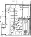
図1および図2に示されているように、バッチ式CVD装置10は略直方体形状に構築された筐体11を備えており、筐体11は大気圧を維持可能な気密性能を有するように構成されている。
筐体11の正面壁12の下部には開口部としての正面メンテナンス口13が人が通過可能な大きさに開設されており、正面壁12の正面側には正面メンテナンス口13の正面側を開閉する開閉手段としての第一正面メンテナンス扉14aおよび第二正面メンテナンス扉14bがそれぞれ建て付けられている。
すなわち、第一正面メンテナンス扉14aの右側端辺は正面壁12の正面側の右側端辺にヒンジ15aによって回動自在に支承されており、第二正面メンテナンス扉14bの左側端辺は正面壁12の正面側の左側端辺にヒンジ15bによって回動自在に支承されている。第一正面メンテナンス扉14aはヒンジ15aを中心にして反時計回りに開かれるようになっており、第二正面メンテナンス扉14bはヒンジ15bを中心にして時計回りに開かれるようになっている(図1の想像線を参照)。
正面壁12の中間高さにはポッド搬入搬出口16が開設されており、正面壁12のポッド搬入搬出口16の手前にはポッドステージ17が構築されている。図1に想像線で示されているように、ポッドステージ17は時計回りに回動するようになっている。
なお、ポッドステージ17にはポッド2がRGV等の工程内搬送装置によって供給および排出されるようになっている。As shown in FIG. 1 and FIG. 2, the batch
A
That is, the right side edge of the first
A pod loading /
The
筐体11の正面壁12の後側にはポッド搬送装置18が設置されており、ポッド搬送装置18はリニアアクチュエータやエレベータおよびスカラ形ロボット等によって構成されている。
ポッド搬送装置18は筐体11の前側空間において左側に偏らされて配置されている。このようにポッド搬送装置18が左側に偏って配置されることにより、筐体11の前側空間の右部分にはメンテナンス通路19が形成されている。
ポッド搬送装置18はポッドステージ17と回転式ポッド棚20とポッドオープナ30の載置台31との間でポッド2を搬送するように構成されている。
図2に示されているように、回転式ポッド棚20は筐体11内のポッド搬送装置18の後側上部に配置されており、複数台のポッド2を一時的に保管し得るように構成されている。すなわち、回転式ポッド棚20は回転する支柱21と、複数台のポッド2を保持する複数枚の棚板22とを備えており、複数枚の棚板22が支柱21に複数段に配置されて水平に固定されている。A
The
The
As shown in FIG. 2, the
筐体11内の回転式ポッド棚20の下側には移載室筐体23が構築されており、回転式ポッド棚20は移載室筐体23の天井壁23aの上に垂直に立設されている。移載室筐体23はポッド搬送装置18や回転式ポッド棚20の設置空間から流体的に隔絶された移載室24を構成している。
移載室24にはウエハ1を移載するウエハ移載装置25が水平に設置されている。ウエハ移載装置25はスカラ形ロボット(selective compliance assembly robot arm 。SCARA)によって構成されており、ウエハ1をツィーザ25aによって下から掬いとって三次元方向に搬送するように構成されている。A
A wafer transfer device 25 for transferring the wafer 1 is horizontally installed in the
移載室筐体23の正面壁23bには上下で一対のウエハ搬入搬出口26、26と移載室メンテナンス口27とが、左右に隣り合わせに配置されてそれぞれ開設されている。正面壁23bは移載室メンテナンス口27の部分において右端が奥に行くように屈曲されている。
上下のウエハ搬入搬出口26、26は左側に偏って配置されており、上下のウエハ搬入搬出口26、26はウエハ1を移載室24に対して搬入搬出し得るように構成されている。移載室メンテナンス口27は偏りの反対側である右側部分に配置されており、移載室メンテナンス口27は人が通過可能な大きさに開設されている。移載室メンテナンス口27はメンテナンス通路19に連絡するようになっている。
正面壁23bには移載室メンテナンス口27を開閉する開閉手段としての移載室メンテナンス扉28が建て付けられている。すなわち、移載室メンテナンス扉28の右側端辺は正面壁23bの右側端辺にヒンジ29によって回動自在に支承されており、移載室メンテナンス扉28はヒンジ29を中心にして反時計回りに開かれるようになっている(図1の想像線を参照)。
また、移載室メンテナンス扉28を閉じた際は、充分な気密性を有しており、メンテナンス通路19側と移載室24とは充分に隔離されるようになっている。On the
The upper and lower wafer loading / unloading
A transfer
In addition, when the transfer
移載室筐体23の正面壁23bの上下のウエハ搬入搬出口26、26には、上下で一対のポッドオープナ30、30が設置されている。
ポッドオープナ30はウエハ搬入搬出口26の正面側の下端辺に水平に突設されてポッド2を載置する載置台31と、載置台31に載置されたポッド2のキャップを着脱するキャップ着脱機構32とを備えており、載置台31に載置されたポッド2のキャップをキャップ着脱機構32によって着脱することにより、ポッド2のウエハ出し入れ口を開閉するようになっている。A pair of
The
図1に示されているように、移載室24のウエハ移載装置25側と反対側である右側端部には、クリーンエア33を吹き出すクリーンユニット34が設置されており、ウエハ移載装置25とクリーンユニット34との間には、基板整合装置としてのノッチ合わせ装置35が設置されている。
クリーンユニット34から吹き出されたクリーンエア33は、ノッチ合わせ装置35およびウエハ移載装置25を流通した後に、筐体11の右後隅に設置された排気装置36によって吸い込まれて、筐体11の外部に排気されるようになっている。
なお、クリーンユニット34から吹き出された後に、図示しない窒素ガス供給手段により窒素ガスを供給させつつ、ノッチ合わせ装置35およびウエハ移載装置25を流通した後に、図示しないウエハ移載装置25の左側のダクトにより吸い込ませて、筐体11の外気に排気させるようにしてもよい。As shown in FIG. 1, a
The
Note that after being blown out from the
筐体11内の移載室24の後側には、大気圧未満の圧力(以下、負圧という。)を維持可能な気密性能を有する筐体(以下、耐圧筐体という。)40が設置されており、この耐圧筐体40によりボートを収納可能な容積を有するロードロック方式の待機室であるロードロック室41が形成されている。
耐圧筐体40の正面壁にはウエハ搬入搬出口42が開設されており、ウエハ搬入搬出口42はゲートバルブ43によって開閉されるようになっている。耐圧筐体40の一対の側壁にはロードロック室41へ窒素(N2 )ガスを給気するためのガス供給管44と、ロードロック室41を負圧に排気するための排気管45とがそれぞれ接続されている。On the rear side of the
A wafer loading / unloading
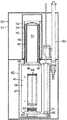
図2および図3に示されているように、ロードロック室41の天井壁にはボート搬入搬出口46が開設されており、ボート搬入搬出口46はボート搬入搬出口46よりも大径の円板形状に形成された炉口ゲートバルブ47により開閉されるように構成されている。
耐圧筐体40の前面壁における上端部には炉口ゲートバルブ出入り口48が、炉口ゲートバルブ47の直径および厚さよりも大きめの横長の長方形に開設されており、耐圧筐体40の前面壁の外側には炉口ゲートバルブ47をボート搬入搬出口46の開放時に収容する炉口ゲートバルブカバー49が炉口ゲートバルブ出入り口48を閉塞するように取り付けられている。
炉口ゲートバルブカバー49は、厚さおよび横幅が炉口ゲートバルブ出入り口48の高さおよび間口よりも大きい容積を有する半円形であって、半円形の弦に相当する側壁が開口した筐体形状に形成されている。炉口ゲートバルブカバー49の開口した側壁の右端は炉口ゲートバルブ出入り口48の一端に設置されたヒンジ(図示せず)によって水平面内で回動するように支承されている。
炉口ゲートバルブカバー49は通常の炉口ゲートバルブ出入り口48の閉鎖時には、シールリングを介して耐圧筐体40の前面に当接された状態で締結具によって締結されており、耐圧筐体40の前面から前方に迫り出した状態になっている。As shown in FIGS. 2 and 3, a boat loading / unloading
At the upper end of the front wall of the pressure-
The furnace gate
The furnace port
耐圧筐体40の上方にはヒータユニット設置筐体50が構築されており、ヒータユニット設置筐体50のヒータユニット設置室51には、処理室53を加熱するヒータユニット52が垂直方向に設置されている。 A heater
図3に示されているように、ヒータユニット52の内部には処理室53を形成するプロセスチューブ54が設置されている。
プロセスチューブ54は石英(SiO2 )が使用されて上端が閉塞し下端が開口した円筒形状に形成されたアウタチューブ55と、石英または炭化シリコン(SiC)が使用されて上下両端が開口した円筒形状に形成されたインナチューブ56とを備えており、アウタチューブ55がインナチューブ56に同心円に被せられている。
アウタチューブ55とインナチューブ56との間には環状の排気路57が両者の間隙によって形成されている。プロセスチューブ54は耐圧筐体40の天井壁の上にマニホールド58を介して支持されており、マニホールド58はボート搬入搬出口46に同心円に配置されている。
図2に示されているように、マニホールド58にはプロセスチューブ54の内部を排気するための排気管59が接続されている。
なお、図示は省略するが、バッチ式CVD装置10は処理室53に原料ガスやパージガス等を導入するためのガス導入管と、プロセスチューブ54の内部の温度を測定してヒータユニット52をフィードバック制御する熱電対とを備えている。As shown in FIG. 3, a process tube 54 forming a
The process tube 54 is made of quartz (SiO2 ) and has an
An annular exhaust passage 57 is formed between the
As shown in FIG. 2, an
Although not shown in the figure, the batch
図1および図3に示されているように、耐圧筐体40にはボートを昇降させるためのボートエレベータ60が設置されており、ボートエレベータ60は送りねじ装置やベローズ等によって構成されている。
ボートエレベータ60の昇降台61の側面にはアーム62が水平に突設されており、アーム62の先端にはシールキャップ63が水平に据え付けられている。
シールキャップ63はプロセスチューブ54の炉口になる耐圧筐体40のボート搬入搬出口46を気密シールするように構成されている。As shown in FIGS. 1 and 3, the pressure-
An
The
シールキャップ63の上には基板保持具としてのボート64が垂直に支持されている。ボート64は複数枚(例えば、25枚、50枚、100枚、125枚、150枚)のウエハ1をその中心を揃えて水平に支持した状態で、ボートエレベータ60によるシールキャップ63の昇降に伴ってプロセスチューブ54の処理室53に対して搬入搬出するように構成されている。
また、ボート64はシールキャップ63に設置されたロータリーアクチュエータ65によって回転されるように構成されている。
図1に示されているように、ボート64に保持されたウエハ1の中心とポッドオープナ30の載置台31に載置されたポッド2のウエハ1の中心とを結ぶ線分は、筐体11の幅方向の中心線に対して幅方向の左方側に偏るように、ボート64およびポッドオープナ30の載置台31は配設されている。
また、ウエハ移載装置25の水平方向の回転中心は、ボート64の上のウエハ1の中心とポッドオープナ30の上のポッド2のウエハ1の中心とを結ぶ線分の上に配置されている。On the
Further, the
As shown in FIG. 1, a line segment connecting the center of the wafer 1 held by the
The horizontal rotation center of the wafer transfer device 25 is arranged on a line segment connecting the center of the wafer 1 on the
耐圧筐体40の背面壁にはロードロック室メンテナンス口66が縦長の長方形に大きく開設されており、背面壁の外面にはロードロック室メンテナンス口66を閉塞するメンテナンス扉67が取り付けられている。
メンテナンス扉67はロードロック室メンテナンス口66を負圧を維持して閉塞することができるように構成されている。
筐体11の背面壁には背面メンテナンス口68が縦長の長方形に大きく開設されており、背面壁の外面には背面メンテナンス口68を閉塞する背面メンテナンス扉69が取り付けられている。A load lock
The
A
移載室筐体23の天井壁23aにおける炉口ゲートバルブカバー49の前方には、炉口ゲートバルブカバー49をメンテナンスするための開口部としてのメンテナンス口70が開設されており、天井壁23aにはメンテナンス口70を開閉可能な開閉手段としてのメンテナンス扉71が取り付けられている。 A
以下、前記構成に係るバッチ式CVD装置を使用したICの製造方法における成膜工程を説明する。
なお、本実施の形態においては、一台のポッド2に収納された25枚以内のプロダクトウエハ1をバッチ処理(一括処理)する場合について説明する。Hereinafter, a film forming process in an IC manufacturing method using the batch type CVD apparatus according to the above configuration will be described.
In the present embodiment, a case will be described in which batch processing (batch processing) of up to 25 product wafers 1 housed in one
成膜すべきウエハ1は25枚以内がポッド2に収納された状態で、バッチ式CVD装置10のポッドステージ17へ工程内搬送装置によって搬送されて来る。
搬送されて来たポッド2はポッドステージ17から回転式ポッド棚20の指定された場所にポッド搬送装置18によって搬送されて保管される。The wafer 1 to be deposited is transported to the
The transported
ウエハ1が収納されたポッド2は、ポッドオープナ30の載置台31の上へポッド搬送装置18によって搬送されて載置される。載置されたポッド2の内外へウエハ1が出し入れされるウエハ出し入れ口を蓋するキャップが、ポッドオープナ30のキャップ着脱機構32によって取り外され、ポッド2のウエハ出し入れ口が開放される。
ポッド2がポッドオープナ30によって開放されると、ロードロック室41のウエハ搬入搬出口42がゲートバルブ43によって開放される。このとき、ロードロック室41は窒素ガスが充満された所謂窒素ガスパージ雰囲気に維持されており、圧力が略大気圧に維持されている。The
When the
ポッド2がポッドオープナ30により開放されると、ウエハ1はポッド2からウエハ移載装置25によってウエハ搬入搬出口26を通じてピックアップされ、移載室24に搬入される。
移載室24に搬入されたウエハ1はノッチ合わせ装置35に載置され、ウエハ1のノッチをノッチ合わせ装置35にて合わせた後に再びウエハ移載装置25によりピックアップされ、ウエハ搬入搬出口42を通じてロードロック室41に搬入され、ボート64へ移載されて装填(ウエハチャージング)される。
この移載作業が繰り返されることにより、ポッド2の全てのウエハ1がボート64にウエハ移載装置25によって装填される。
空になったポッド2はポッドオープナ30の載置台31から回転式ポッド棚20にポッド搬送装置18によって一時的に戻される。When the
The wafer 1 carried into the
By repeating this transfer operation, all the wafers 1 in the
The
ウエハ搬入搬出口42がゲートバルブ43によって閉じられると、ロードロック室41は排気管45によって真空引きされることにより、減圧される。この際、ロードロック室41は移載室24から隔絶されているので、減圧時間は短くて済む。 When the wafer loading / unloading
ロードロック室41が所定の負圧に減圧されると、ボート搬入搬出口46が炉口ゲートバルブ47によって開放される。このとき、炉口ゲートバルブ47は炉口ゲートバルブ出入り口48から炉口ゲートバルブカバー49の内部に搬入されて収容される。 When the
続いて、シールキャップ63がボートエレベータ60の昇降台61によって上昇されて、シールキャップ63に支持されたボート64がプロセスチューブ54の処理室53に搬入(ボートローディング)される。
ボート64が上限に達すると、ボート64を支持したシールキャップ63の上面の周辺部がボート搬入搬出口46をシール状態に閉塞するため、処理室53は気密に閉じられた状態になる。
ボート64の処理室53への搬入に際して、ロードロック室41は負圧に維持されているため、ボート64の処理室53への搬入に伴って外部の酸素や水分が処理室53に侵入することは確実に防止される。Subsequently, the
When the
When the
その後、プロセスチューブ54の処理室53は気密に閉じられた状態で、所定の圧力となるように排気管59によって排気され、ヒータユニット52によって所定の温度に加熱され、所定の原料ガスがガス導入管によって所定の流量だけ供給される。
これにより、予め設定された処理条件に対応する所望の膜がウエハ1に形成される。Thereafter, the
As a result, a desired film corresponding to preset processing conditions is formed on the wafer 1.
ウエハ1に対する成膜ステップについて設定された処理時間が経過すると、処理室53は窒素ガスによって置換された後に、ボート64がボートエレベータ60によって下降されることにより、処理済みウエハ1を保持したボート64がロードロック室41に搬出(ボートアンローディング)される。 When the processing time set for the film forming step for the wafer 1 elapses, the
ボート64がロードロック室41に排出されると、ボート搬入搬出口46が炉口ゲートバルブ47によって閉鎖され、ロードロック室41が窒素ガスパージされる。
他方、空のポッド2が回転式ポッド棚20からポッドオープナ30の載置台31にポッド搬送装置18によって搬送されて移載される。When the
On the other hand, the
ロードロック室41が窒素ガスパージ雰囲気の圧力が略大気圧に維持されると、ウエハ搬入搬出口42がゲートバルブ43によって開放される。また、ポッドオープナ30の載置台31の上の空のポッド2のキャップがキャップ着脱機構32によって開放される。
続いて、搬出されたボート64の処理済みウエハ1がウエハ移載装置25によって脱装(ディスチャージング)されて、大気圧に維持された移載室24に搬入される。搬入された処理済みのウエハ1は、ポッドオープナ30の空のポッド2にウエハ移載装置25によって収納される。When the pressure of the nitrogen gas purge atmosphere in the
Subsequently, the processed wafer 1 of the unloaded
ボート64の処理済みウエハ1がポッド2に全て収納されると、ポッド2はポッドオープナ30のキャップ着脱機構32によってキャップを装着された後に、載置台31から回転式ポッド棚20にポッド搬送装置18によって搬送される。 When all the processed wafers 1 of the
その後に、処理済みウエハ1を収納したポッド2は回転式ポッド棚20からポッドステージ17に搬送され、ポッドステージ17から次の処理工程へ工程内搬送装置によって搬送されて行く。 Thereafter, the
以降、前述した作用が繰り返されて、ウエハ1が25枚ずつ、バッチ式CVD装置10によってバッチ処理されて行く。 Thereafter, the above-described operation is repeated, and 25 wafers 1 are batch processed by the batch
ところで、例えば、ウエハ移載装置25のセラミック製のツィーザ25aが破損した場合には、ツィーザ25aを交換する必要がある。
このように移載室24におけるメンテナンスを実施する場合には、図1に想像線で示されているように、まず、第一正面メンテナンス扉14aがヒンジ15aを中心にして前方に水平に回動されることにより、正面メンテナンス口13の右側が開放される。
次に、図1に想像線で示されているように、移載室メンテナンス扉28がヒンジ29を中心に前方に回動されることにより、移載室メンテナンス口27が開かれる。
その後に、移載室24のウエハ移載装置25のツィーザ25aの交換作業が、正面メンテナンス口13、メンテナンス通路19および移載室メンテナンス口27を通じて実施される。By the way, for example, when the ceramic tweezer 25a of the wafer transfer device 25 is damaged, it is necessary to replace the tweezer 25a.
When carrying out maintenance in the
Next, as indicated by an imaginary line in FIG. 1, the transfer
Thereafter, the replacement work of the tweezer 25 a of the wafer transfer device 25 in the
炉口ゲートバルブカバー49のメンテナンスは、正面メンテナンス口13、メンテナンス通路19、炉口ゲートバルブカバー用のメンテナンス口70を通じて実施される。 Maintenance of the furnace port
ボート64やプロセスチューブ54のフルクリーニング(ウエットエッチングによる洗浄)等を実施する場合には、まず、筐体11の背面壁の背面メンテナンス口68がメンテナンス扉69によって開放される。
続いて、耐圧筐体40の背面壁のロードロック室メンテナンス口66がメンテナンス扉67によって開放される。
その後に、ボート64やプロセスチューブ54の交換作業がロードロック室メンテナンス口66および68を通じて実施される。When full cleaning (cleaning by wet etching) or the like of the
Subsequently, the load lock
Thereafter, the replacement work of the
前記実施の形態によれば、次の効果が得られる。 According to the embodiment, the following effects can be obtained.
1) 移載室の正面壁に移載室メンテナンス口を開設するとともに、移載室メンテナンス口を開閉するメンテナンス扉を配設することにより、移載室内のメンテナンス作業を移載室メンテナンス口を通じて実施することができるので、メンテナンス扉が移載室の側面に設置された場合に移載室の側方に必要であるメンテナンスエリアと、作業者が出入りするための通路部分とを省略することができる。その結果、バッチ式CVD装置のフットプリントを減少させることができる。1) In addition to opening a transfer chamber maintenance port on the front wall of the transfer chamber and installing a maintenance door that opens and closes the transfer chamber maintenance port, maintenance work in the transfer chamber is performed through the transfer chamber maintenance port. Therefore, when the maintenance door is installed on the side surface of the transfer chamber, the maintenance area required on the side of the transfer chamber and the passage portion for the operator to enter and exit can be omitted. . As a result, the footprint of the batch type CVD apparatus can be reduced.
2) ボートに保持されたウエハの中心とポッドオープナに載置されたポッドのウエハの中心とを結ぶ線分を筐体の幅方向の中心線に対して幅方向の一方側(左側)に偏らせ、移載室の正面壁の反対側(右側)にメンテナンス扉によって開閉される移載室メンテナンス口を配設することにより、ロードロック室と移載室とポッドオープナとが筐体内に背面側から順に配設されたバッチ式CVD装置であっても、無駄にフットプリントを増やすことなく、かつ、移載室に内部に設置されたウエハ移載装置やノッチ合わせ装置等をロードロック室を通らずにメンテナンスすることができるので、それらのメンテナンス作業を容易に実施することができる。2) The line connecting the center of the wafer held by the boat and the center of the wafer of the pod placed on the pod opener is biased to one side (left side) in the width direction with respect to the center line in the width direction of the housing. By installing a transfer chamber maintenance port that is opened and closed by a maintenance door on the opposite side (right side) of the front wall of the transfer chamber, the load lock chamber, transfer chamber, and pod opener are placed in the rear side of the housing. Even in the case of batch-type CVD devices arranged in order, the wafer transfer device and notch alignment device installed inside the transfer chamber are passed through the load lock chamber without increasing the footprint. Therefore, the maintenance work can be easily performed.
3) また、移載室をメンテナンスする際にロードロック室を外気にさらす必要がないため、その際にロードロック室内が汚染するのを防止することができる。さらに、ロードロック室を通路とする必要がないため、ロードロック室のサイズを小さくすることができ、減圧および窒素ガス置換における時間を短縮することができる。3) Moreover, since it is not necessary to expose the load lock chamber to the outside air when maintaining the transfer chamber, it is possible to prevent the load lock chamber from being contaminated at that time. Furthermore, since there is no need to use the load lock chamber as a passage, the size of the load lock chamber can be reduced, and the time required for decompression and nitrogen gas replacement can be shortened.
4) 筐体の正面壁を開閉するように構成することにより、ポッド搬送装置やポッドオープナ等のメンテナンスを容易に実施することができるとともに、その奥に設けられた移載室メンテナンス口へのアクセス通路を確保することができる。4) By configuring the front wall of the housing to open and close, maintenance of the pod transfer device, pod opener, etc. can be easily performed, and access to the transfer chamber maintenance port provided in the back of the device is possible. A passage can be secured.
5) 正面メンテナンス扉を幅方向に二つに分け、片側をポッドステージと略同じ幅とし、他方側をメンテナンス通路と略同じ幅に設定することにより、移載室や炉口ゲートバルブ等のメンテナンスをする際に、他方側のみを開くだけでメンテナンスすることができるので、作業効率を向上させることができる。5) By dividing the front maintenance door into two in the width direction and setting one side to be approximately the same width as the pod stage and the other side to be approximately the same width as the maintenance passage, maintenance of the transfer chamber, furnace gate valve, etc. Since the maintenance can be performed only by opening only the other side, working efficiency can be improved.
6) 移載室にクリーンユニットとノッチ合わせ装置とウエハ移載装置とをクリーンエアの流れ方向に順に配設することにより、ノッチ合わせ装置およびウエハ移載装置をクリーンエアによって効果的にクリーニングすることができるので、ウエハおよびバッチ式CVD装置の清浄度を向上させることができる。すなわち、ノッチ合わせ装置とウエハ移載装置とを比較したとき、ウエハ移載装置の方が遥かに大きく動作するため、パーティクルを発生し巻き上げることが多く、それ故、ウエハ移載装置をクリーンユニットから見て下流側とすることにより、クリーンエアによって効果的にクリーニングすることができる。6) Cleaning the notch alignment device and the wafer transfer device with clean air effectively by arranging the clean unit, the notch alignment device and the wafer transfer device in order in the flow direction of the clean air in the transfer chamber. Therefore, the cleanliness of the wafer and the batch type CVD apparatus can be improved. That is, when comparing the notch alignment device and the wafer transfer device, the wafer transfer device operates much more greatly, so it often generates and rolls up particles, so the wafer transfer device is removed from the clean unit. By setting it to the downstream side, it is possible to effectively clean with clean air.
7) 移載室メンテナンス口および移載室メンテナンス扉を水平方向から見てクリーンユニット側に近くなるに従って移載室の空間を漸次小さくするように配置することにより、クリーニングするスペース(容積)を小さく抑制することができるとともに、クリーンユニットから吹き出されたクリーンエアの淀みの発生等を防止してクリーンエアを移載室全体に拡散することができるので、クリーンエアのクリーニング効果を向上させることができる。7) By arranging the transfer chamber maintenance port and the transfer chamber maintenance door so that the space in the transfer chamber gradually decreases as it approaches the clean unit side when viewed from the horizontal direction, the cleaning space (volume) is reduced. It is possible to suppress the occurrence of stagnation of clean air blown out from the clean unit and to diffuse clean air throughout the transfer chamber, so that the clean air cleaning effect can be improved. .
8) クリーンユニットの近傍に移載室メンテナンス口を配設することにより、クリーンユニットのメンテナンス作業を簡単に実施することができる。8) By placing the transfer chamber maintenance port near the clean unit, the clean unit can be easily maintained.
9) 処理室を開閉する炉口ゲートバルブを囲う炉口ゲートバルブカバーを移載室の上に突設するとともに、移載室の上方に炉口ゲートバルブカバーをメンテナンスするためのメンテナンス口およびメンテナンス扉を配設することにより、炉口ゲートバルブカバーおよび炉口ゲートバルブのメンテナンス作業を移載室やロードロック室を通らずに実施することができる。9) A furnace port gate valve cover that surrounds the furnace port gate valve that opens and closes the processing chamber is projected above the transfer chamber, and a maintenance port and maintenance for maintaining the furnace port gate valve cover above the transfer chamber By providing the door, maintenance work of the furnace port gate valve cover and the furnace port gate valve can be performed without passing through the transfer chamber or the load lock chamber.
図4は本発明の他の実施の形態であるバッチ式CVD装置を示す平面断面図である。 FIG. 4 is a plan sectional view showing a batch type CVD apparatus according to another embodiment of the present invention.
本実施の形態が前記実施の形態と異なる点は、ポッドオープナ30上のウエハ1の中心とウエハ移載装置25上のウエハの中心とボート64上のウエハ1の中心とを通る線分が、筐体11の幅方向の中心線に対して右側に偏っており、移載室メンテナンス口27Aおよび移載室メンテナンス扉28Aが移載室24の背面壁の左端部において外部に面して配設されている点、である。 This embodiment is different from the above embodiment in that a line segment passing through the center of the wafer 1 on the
本実施の形態においても、移載室24へは移載室メンテナンス口27Aを通じて直接的にアクセスすることができるので、前記実施の形態と同様の効果を得ることができる。 Also in this embodiment, since the
なお、本発明は前記実施の形態に限定されるものではなく、その要旨を逸脱しない範囲で種々に変更が可能であることはいうまでもない。 Needless to say, the present invention is not limited to the above-described embodiment, and various modifications can be made without departing from the scope of the invention.
例えば、開口部としてのメンテナンス口を開閉する開閉手段は、扉構造に構成するに限らず、カバー等の構造に構成してもよい。 For example, the opening / closing means for opening and closing the maintenance port as the opening is not limited to the door structure, and may be configured to have a structure such as a cover.
ポッドオープナの設置箇所と移載室メンテナンス口の開設箇所とは、図1に示すように同じ面とするのみならず、上下にずらしてもよい。 The location where the pod opener is installed and the location where the transfer chamber maintenance port is opened are not only on the same plane as shown in FIG.
ボートが待機する待機室はロードロック室に構成するに限らず、大気圧を維持可能な気密室に構成してもよい。 The standby chamber where the boat waits is not limited to the load lock chamber, but may be configured to be an airtight chamber capable of maintaining atmospheric pressure.
なお、移載室内に設置されているノッチ合わせ装置やウエハ移載装置、耐圧筐体のウエハ搬入搬出口を開閉するゲートバルブ等は、取り付け取り外し可能となっており、これらは変換や移載室外でメンテナンスする際には、ノッチ合わせ装置やウエハ移載装置およびゲートバルブ等を取り外して、移載室メンテナンス口から移載室外へ持ち出すことができるような移載室メンテナンス口および移載室メンテナンス扉のサイズとするとより、メンテナンス作業が有効にし易くなる。 Note that the notch alignment device, wafer transfer device, and gate valve that opens and closes the wafer loading / unloading port of the pressure-resistant housing can be attached and removed. When performing maintenance, the transfer chamber maintenance port and transfer chamber maintenance door can be taken out of the transfer chamber maintenance port by removing the notch alignment device, wafer transfer device, gate valve, etc. Therefore, the maintenance work is more effective.
前記実施の形態ではバッチ式CVD装置の場合について説明したが、本発明はこれに限らず、基板処理装置全般に適用することができる。 In the above embodiment, the case of a batch type CVD apparatus has been described. However, the present invention is not limited to this and can be applied to all substrate processing apparatuses.
本発明の好ましい態様を付記する。
(1)ロードロック室と移載室とが筐体内に背面側から順に配設されており、前記移載室の背面側であって前記ロードロック室の配設されない箇所には、開口部とこの開口部を開閉する開閉手段とが配設されていることを特徴とする基板処理装置。
(2)前記開口部は前記移載室内をメンテナンスするために設けられていることを特徴とする(1)に記載の基板処理装置。
(3)前記開口部は人が通過可能な大きさに設定されていることを特徴とする(1)または(2)に記載の基板処理装置。
(4)前記開閉手段は前記筐体外と面していることを特徴とする(1)、(2)または(3)に記載の基板処理装置。
(5)ロードロック室と、基板を移載する基板移載装置が設置された移載室とが筐体内に背面側から順に配設されており、前記移載室の背面側であって前記ロードロック室の配設されない箇所には、前記基板移載装置をメンテナンスするための開口部と、この開口部を開閉する開閉手段が配設されていることを特徴とする基板処理装置。
(6)基板を基板保持具に保持しつつ待機させる待機室と、移載室と、前記基板を収容するキャリアを載置するキャリア載置手段とが筐体内に背面側から順に配設されており、前記基板保持具に保持された前記基板の中心と、前記キャリア載置手段に載置された前記キャリアの前記基板の中心を結ぶ線分とが、前記筐体の幅方向の中心線に対して幅方向の一方側に偏っており、偏っていない他方側の前記移載室の正面側または背面側には、開口部とこの開口部を開閉する開閉手段が配設されていることを特徴とする基板処理装置。
(7)前記移載室内の前記一方側には前記基板を移載する基板移載装置が配置され、前記他方側には前記基板を整合する基板整合装置が配置されていることを特徴とする(6)に記載の基板処理装置。
(8)前記基板移載装置の水平方向の回転中心は、前記線分上に配置されていることを特徴とする(6)または(7)に記載の基板処理装置。
(9)前記開口部は前記移載室内をメンテナンスするために設けられていることを特徴とする(6)に記載の基板処理装置。
(10)前記開口部は前記基板移載装置および前記基板整合装置をメンテナンスするために設けられていることを特徴とする(6)ないし(9)のいずれかに記載の基板処理装置。
(11)前記開口部は人が通過可能な大きさに設定されていることを特徴とする(6)ないし(10)のいずれかに記載の基板処理装置。
(12)前記待機室はロードロック室であることを特徴とする(6)ないし(11)のいずれかに記載の基板処理装置。
(13)待機室と移載室とが筐体内に背面側から順に配設されており、前記移載室には前記移載室の雰囲気を清浄するクリーンユニットと、基板を整合する基板整合装置と、前記基板を移載する基板移載装置とが、前記クリーンユニットから吹き出される雰囲気の流れ方向に順に配設されていることを特徴とする基板処理装置。
(14)前記移載室の正面または背面の前記クリーンユニットの近傍には、開口部とこの開口部を開閉する開閉手段とが配設されていることを特徴とする(13)に記載の基板処理装置。
(15)前記開口部は前記移載室内をメンテナンスするために設けられていることを特徴とする(13)または(14)に記載の基板処理装置。
(16)前記開口部は前記基板移載装置および前記基板整合装置をメンテナンスするために設けられていることを特徴とする(13)ないし(15)のいずれかに記載の基板処理装置。
(17)前記開口部は人が通過可能な大きさに設定されていることを特徴とする(13)ないし(16)のいずれかに記載の基板処理装置。
(18)前記待機室はロードロック室であることを特徴とする(13)ないし(17)のいずれかに記載の基板処理装置。
(19)前記ロードロック室の上方には前記基板を処理する処理室が配置されていることを特徴とする(1)ないし(5)、(12)のいずれかに記載の基板処理装置。
(20)前記待機室の上方には前記基板を処理する処理室が配置されていることを特徴とする(6)ないし(11)、(13)〜(17)のいずれかに記載の基板処理装置。
(21)前記処理室よりも正面側には前記処理室を開閉する炉口ゲートバルブを囲う炉口ゲートバルブカバーが突設されており、前記移載室の上方には前記炉口ゲートバルブカバーをメンテナンスするための開口部と、この開口部を開閉可能な開閉手段とが設けられていることを特徴とする(19)または(20)に記載の基板処理装置。
(22)前記開口部および開閉手段は水平方向から見て前記クリーンユニット側に近くなるに従って前記移載室の空間を漸次小さくするように配置されていることを特徴とする(1)ないし(21)のいずれかに記載の基板処理装置。
(23)ロードロック室と移載室とが筐体内に背面側から順に配設されているとともに、前記ロードロック室の上方に配設され基板を処理する処理室と、前記処理室を加熱するヒータユニットと、前記処理室にガスを供給するガス供給管と、前記処理室を排気する排気管とを備えており、前記移載室の背面側であって前記ロードロック室の配設されない箇所には、開口部とこの開口部を開閉する開閉手段が配設されていることを特徴とする基板処理装置。
(24)ロードロック室と移載室とが筐体内に背面側から順に配設されているとともに、前記ロードロック室の上方に配設され基板を処理する処理室と、前記処理室を加熱するヒータユニットと、前記処理室にガスを供給するガス供給管と、前記処理室を排気する排気管とを備えており、前記移載室の背面側であって前記ロードロック室の配設されない箇所には、開口部とこの開口部を開閉する開閉手段が配設されている基板処理装置を用いて前記基板を処理する半導体装置の製造方法であって、
前記ヒータユニットによって前記処理室を加熱するステップと、
前記処理室に前記ガス供給管から前記ガスを供給するステップと、
前記基板を処理するステップと、
前記処理室を排気管によって排気するステップと、
を有することを特徴とする半導体装置の製造方法。
(25)ロードロック室と移載室とが筐体内に背面側から順に配設されており、前記ロードロック室が前記筐体の幅方向の中心線に対して幅方向の一方側に偏っており、この一方側と反対側の他方側の前記移載室の背面側には開口部と、この開口部を開閉する開閉手段とが配設されていることを特徴とする基板処理装置。
(26)前記ロードロック室の背面側には前記開口部と、この開口部を開閉する開閉手段とが配設されていることを特徴とする(25)に記載の基板処理装置。Preferred embodiments of the present invention will be additionally described.
(1) A load lock chamber and a transfer chamber are sequentially disposed in the housing from the back side, and an opening is provided at a position on the back side of the transfer chamber and where the load lock chamber is not disposed. An opening / closing means for opening and closing the opening is disposed.
(2) The substrate processing apparatus according to (1), wherein the opening is provided to maintain the transfer chamber.
(3) The substrate processing apparatus according to (1) or (2), wherein the opening is set to a size that allows a person to pass through.
(4) The substrate processing apparatus according to (1), (2) or (3), wherein the opening / closing means faces the outside of the housing.
(5) A load lock chamber and a transfer chamber in which a substrate transfer device for transferring a substrate is installed are sequentially arranged in the housing from the back side, and the back side of the transfer chamber A substrate processing apparatus, wherein an opening for maintaining the substrate transfer device and an opening / closing means for opening and closing the opening are provided at a location where the load lock chamber is not provided.
(6) A standby chamber for holding the substrate while holding it on the substrate holder, a transfer chamber, and a carrier mounting means for mounting the carrier for storing the substrate are sequentially disposed in the housing from the back side. A line segment connecting the center of the substrate held by the substrate holder and the center of the substrate of the carrier placed on the carrier placing means is a center line in the width direction of the housing On the other hand, it is biased to one side in the width direction, and an opening and an opening / closing means for opening and closing the opening are disposed on the front side or the back side of the transfer chamber on the other side that is not biased. A substrate processing apparatus.
(7) A substrate transfer device for transferring the substrate is disposed on the one side in the transfer chamber, and a substrate alignment device for aligning the substrate is disposed on the other side. The substrate processing apparatus according to (6).
(8) The substrate processing apparatus according to (6) or (7), wherein a horizontal rotation center of the substrate transfer apparatus is arranged on the line segment.
(9) The substrate processing apparatus according to (6), wherein the opening is provided for maintenance of the transfer chamber.
(10) The substrate processing apparatus according to any one of (6) to (9), wherein the opening is provided for maintaining the substrate transfer apparatus and the substrate alignment apparatus.
(11) The substrate processing apparatus according to any one of (6) to (10), wherein the opening is set to a size that allows a person to pass through.
(12) The substrate processing apparatus according to any one of (6) to (11), wherein the standby chamber is a load lock chamber.
(13) A standby chamber and a transfer chamber are sequentially disposed in the housing from the back side, and the transfer chamber has a clean unit for cleaning the atmosphere of the transfer chamber and a substrate alignment apparatus for aligning the substrates. And a substrate transfer apparatus for transferring the substrate in order in the flow direction of the atmosphere blown from the clean unit.
(14) The substrate according to (13), wherein an opening and an opening / closing means for opening and closing the opening are disposed in the vicinity of the clean unit on the front or back of the transfer chamber. Processing equipment.
(15) The substrate processing apparatus according to (13) or (14), wherein the opening is provided to maintain the transfer chamber.
(16) The substrate processing apparatus according to any one of (13) to (15), wherein the opening is provided for maintaining the substrate transfer apparatus and the substrate alignment apparatus.
(17) The substrate processing apparatus according to any one of (13) to (16), wherein the opening is set to a size that allows a person to pass through.
(18) The substrate processing apparatus according to any one of (13) to (17), wherein the standby chamber is a load lock chamber.
(19) The substrate processing apparatus according to any one of (1) to (5) and (12), wherein a processing chamber for processing the substrate is disposed above the load lock chamber.
(20) The substrate processing according to any one of (6) to (11) and (13) to (17), wherein a processing chamber for processing the substrate is disposed above the standby chamber. apparatus.
(21) A furnace port gate valve cover that surrounds a furnace port gate valve that opens and closes the process chamber projects from the front side of the process chamber, and the furnace port gate valve cover is located above the transfer chamber. The substrate processing apparatus according to (19) or (20), wherein an opening for maintaining the substrate and an opening / closing means capable of opening and closing the opening are provided.
(22) The opening and the opening / closing means are disposed so as to gradually reduce the space of the transfer chamber as it approaches the clean unit side when viewed in the horizontal direction. The substrate processing apparatus according to any one of the above.
(23) A load lock chamber and a transfer chamber are sequentially disposed in the housing from the back side, a processing chamber disposed above the load lock chamber for processing a substrate, and heating the processing chamber. A location having a heater unit, a gas supply pipe for supplying gas to the processing chamber, and an exhaust pipe for exhausting the processing chamber, on the rear side of the transfer chamber, where the load lock chamber is not disposed The substrate processing apparatus is provided with an opening and an opening / closing means for opening and closing the opening.
(24) A load lock chamber and a transfer chamber are sequentially disposed in the housing from the back side, a processing chamber disposed above the load lock chamber for processing a substrate, and heating the processing chamber. A location having a heater unit, a gas supply pipe for supplying gas to the processing chamber, and an exhaust pipe for exhausting the processing chamber, on the rear side of the transfer chamber, where the load lock chamber is not disposed Is a method of manufacturing a semiconductor device that processes a substrate using a substrate processing apparatus provided with an opening and an opening / closing means for opening and closing the opening.
Heating the processing chamber by the heater unit;
Supplying the gas from the gas supply pipe to the processing chamber;
Processing the substrate;
Exhausting the processing chamber by an exhaust pipe;
A method for manufacturing a semiconductor device, comprising:
(25) The load lock chamber and the transfer chamber are sequentially disposed in the housing from the back side, and the load lock chamber is biased to one side in the width direction with respect to the center line in the width direction of the housing. An opening and an opening / closing means for opening and closing the opening are disposed on the back side of the transfer chamber on the other side opposite to the one side.
(26) The substrate processing apparatus according to (25), wherein the opening and an opening / closing means for opening and closing the opening are disposed on the back side of the load lock chamber.
1…ウエハ(基板)、2…ポッド(キャリア)、10…バッチ式CVD装置(基板処理装置)、11…筐体、12…正面壁、13…正面メンテナンス口、14a、14b…正面メンテナンス扉、15a、15b…ヒンジ、16…ポッド搬入搬出口、17…ポッドステージ、18…ポッド搬送装置、19…メンテナンス通路、20…回転式ポッド棚、21…支柱、22…棚板、23…移載室筐体、23a…天井壁、23b…正面壁、24…移載室、25…ウエハ移載装置、25a…ツィーザ、26…ウエハ搬入搬出口、27、27A…移載室メンテナンス口(開口部)、28、28A…移載室メンテナンス扉(開閉手段)、29…ヒンジ、30…ポッドオープナ、31…載置台、32…キャップ着脱機構、33…クリーンエア、34…クリーンユニット、35…ノッチ合わせ装置(基板整合装置)、36…排気装置、40…耐圧筐体、41…ロードロック室、42…ウエハ搬入搬出口、43…ゲートバルブ、44…ガス供給管、45…排気管、46…ボート搬入搬出口、47…炉口ゲートバルブ、48…炉口ゲートバルブ出入り口、49…炉口ゲートバルブカバー、50…ヒータユニット設置筐体、51…ヒータユニット設置室、52…ヒータユニット、53…処理室、54…プロセスチューブ、55…アウタチューブ、56…インナチューブ、57…排気路、58…マニホールド、59…排気管、60…ボートエレベータ、61…昇降台、62…アーム、63…シールキャップ、64…ボート(基板保持具)、65…ロータリーアクチュエータ、66…ロードロック室メンテナンス口(開口部)、67…メンテナンス扉(開閉手段)、68…背面メンテナンス口(開口部)、69…背面メンテナンス扉(開閉手段)、70…炉口ゲートバルブカバーメンテナンス口(開口部)、71…メンテナンス扉(開閉手段)。 DESCRIPTION OF SYMBOLS 1 ... Wafer (substrate), 2 ... Pod (carrier), 10 ... Batch type CVD apparatus (substrate processing apparatus), 11 ... Housing, 12 ... Front wall, 13 ... Front maintenance port, 14a, 14b ... Front maintenance door, 15a, 15b ... hinges, 16 ... pod loading / unloading port, 17 ... pod stage, 18 ... pod transfer device, 19 ... maintenance passage, 20 ... rotary pod shelf, 21 ... column, 22 ... shelf plate, 23 ... transfer chamber Case, 23a ... Ceiling wall, 23b ... Front wall, 24 ... Transfer chamber, 25 ... Wafer transfer device, 25a ... Tweezer, 26 ... Wafer loading / unloading port, 27, 27A ... Transfer chamber maintenance port (opening) 28, 28A ... Transfer chamber maintenance door (opening / closing means), 29 ... Hinges, 30 ... Pod opener, 31 ... Place, 32 ... Cap attaching / detaching mechanism, 33 ... Clean air, 34 ...
Claims (3)
Translated fromJapanese前記基板移載装置は、前記移載室内の幅方向一方側に配置され、前記移載室内の前記幅方向他方側には、前記移載室の雰囲気を清浄するクリーンユニットが配置され、前記幅方向他方側の前記移載室の正面または背面には、開口部と該開口部を開閉する開閉手段とが、前記基板移載装置よりも前記クリーンユニットに近くなるに従って前記移載室の空間が漸次小さくなるように配置されていることを特徴とする基板処理装置。A transfer chamber in which a substrate transfer device for transferring a substrate is disposed, a standby chamber disposed on the back surface of the transfer chamber, waiting for the substrate, and a substrate disposed above the standby chamber for processing the substrate. And a processing chamber,
The substrate transfer device is disposed on one side in the width direction in the transfer chamber, and a clean unit for cleaning the atmosphere of the transfer chamber is disposed on the other side in the width direction in the transfer chamber, and the width On the front or back of the transfer chamber on the other side in the direction, an opening and an opening / closing means for opening and closing the opening become closer to the clean unit than the substrate transfer device. A substrate processing apparatus, wherein the substrate processing apparatus is arranged so as to become gradually smaller.
前記基板移載装置は、該移載室内における前記筐体の幅方向の中心線に対して該幅方向一方側に偏って配設され、
前記開口部、前記開閉手段および前記クリーンユニットは、該移載室における前記中心線に対して前記幅方向他方側に偏って配設されていることを特徴とする請求項1に記載の基板処理装置。The transfer chamber, the standby chamber, and the processing chamber are provided in a housing,
The substrate transfer device is disposed so as to be biased to one side in the width direction with respect to a center line in the width direction of the casing in the transfer chamber,
2. The substrate processing according to claim 1, wherein the opening, the opening / closing means, and the clean unit are disposed so as to be biased toward the other side in the width direction with respect to the center line in the transfer chamber. apparatus.
前記移載室の背面に配置された待機室へ前記移載室から基板を移載し、前記待機室から、前記待機室の上方に配設された処理室に基板を搬入するステップと、
前記処理室を加熱し、前記処理室にガスを供給し、排気し、基板を処理するステップと、
を有することを特徴とする半導体装置の製造方法。The substrate transfer device arranged on one side in the width direction in the transfer chamber transfers the substrate and is closer to the clean unit arranged on the other side in the width direction in the transfer chamber than the substrate transfer device. Purging the atmosphere of the transfer chamber by the clean unit with the opening and closing means closed so that the space of the transfer chamber is gradually reduced according to
Transferring a substrate from the transfer chamber to a standby chamber disposed on the back surface of the transfer chamber, and loading the substrate from the standby chamber into a processing chamber disposed above the standby chamber;
Heating the processing chamber, supplying gas to the processing chamber, evacuating, and processing the substrate;
A method for manufacturing a semiconductor device, comprising:
Priority Applications (1)
| Application Number | Priority Date | Filing Date | Title |
|---|---|---|---|
| JP2010140438AJP4763841B2 (en) | 2004-07-13 | 2010-06-21 | Substrate processing apparatus and semiconductor device manufacturing method |
Applications Claiming Priority (3)
| Application Number | Priority Date | Filing Date | Title |
|---|---|---|---|
| JP2004205577 | 2004-07-13 | ||
| JP2004205577 | 2004-07-13 | ||
| JP2010140438AJP4763841B2 (en) | 2004-07-13 | 2010-06-21 | Substrate processing apparatus and semiconductor device manufacturing method |
Related Parent Applications (1)
| Application Number | Title | Priority Date | Filing Date |
|---|---|---|---|
| JP2006528655ADivisionJP4559427B2 (en) | 2004-07-13 | 2005-06-27 | Substrate processing apparatus and semiconductor device manufacturing method |
Publications (2)
| Publication Number | Publication Date |
|---|---|
| JP2010283356A JP2010283356A (en) | 2010-12-16 |
| JP4763841B2true JP4763841B2 (en) | 2011-08-31 |
Family
ID=35783724
Family Applications (2)
| Application Number | Title | Priority Date | Filing Date |
|---|---|---|---|
| JP2006528655AExpired - Fee RelatedJP4559427B2 (en) | 2004-07-13 | 2005-06-27 | Substrate processing apparatus and semiconductor device manufacturing method |
| JP2010140438AExpired - Fee RelatedJP4763841B2 (en) | 2004-07-13 | 2010-06-21 | Substrate processing apparatus and semiconductor device manufacturing method |
Family Applications Before (1)
| Application Number | Title | Priority Date | Filing Date |
|---|---|---|---|
| JP2006528655AExpired - Fee RelatedJP4559427B2 (en) | 2004-07-13 | 2005-06-27 | Substrate processing apparatus and semiconductor device manufacturing method |
Country Status (4)
| Country | Link |
|---|---|
| US (1) | US9111972B2 (en) |
| JP (2) | JP4559427B2 (en) |
| KR (1) | KR100831933B1 (en) |
| WO (1) | WO2006006377A1 (en) |
Families Citing this family (349)
| Publication number | Priority date | Publication date | Assignee | Title |
|---|---|---|---|---|
| JP4606388B2 (en)* | 2006-06-12 | 2011-01-05 | 川崎重工業株式会社 | Transfer system unit for substrate transfer equipment |
| US10378106B2 (en) | 2008-11-14 | 2019-08-13 | Asm Ip Holding B.V. | Method of forming insulation film by modified PEALD |
| US9394608B2 (en) | 2009-04-06 | 2016-07-19 | Asm America, Inc. | Semiconductor processing reactor and components thereof |
| US8802201B2 (en) | 2009-08-14 | 2014-08-12 | Asm America, Inc. | Systems and methods for thin-film deposition of metal oxides using excited nitrogen-oxygen species |
| KR101907433B1 (en)* | 2010-12-14 | 2018-10-12 | 마퍼 리쏘그라피 아이피 비.브이. | Lithography system and method of processing substrates in such a lithography system |
| JP2012169534A (en)* | 2011-02-16 | 2012-09-06 | Hitachi Kokusai Electric Inc | Substrate processing device and method of manufacturing semiconductor device |
| US9312155B2 (en) | 2011-06-06 | 2016-04-12 | Asm Japan K.K. | High-throughput semiconductor-processing apparatus equipped with multiple dual-chamber modules |
| US10854498B2 (en) | 2011-07-15 | 2020-12-01 | Asm Ip Holding B.V. | Wafer-supporting device and method for producing same |
| US20130023129A1 (en) | 2011-07-20 | 2013-01-24 | Asm America, Inc. | Pressure transmitter for a semiconductor processing environment |
| US8888434B2 (en) | 2011-09-05 | 2014-11-18 | Dynamic Micro System | Container storage add-on for bare workpiece stocker |
| US9017481B1 (en) | 2011-10-28 | 2015-04-28 | Asm America, Inc. | Process feed management for semiconductor substrate processing |
| US9997384B2 (en)* | 2011-12-01 | 2018-06-12 | Taiwan Semiconductor Manufacturing Company, Ltd. | Methods for transporting wafers between wafer holders and chambers |
| US9659799B2 (en) | 2012-08-28 | 2017-05-23 | Asm Ip Holding B.V. | Systems and methods for dynamic semiconductor process scheduling |
| US10714315B2 (en) | 2012-10-12 | 2020-07-14 | Asm Ip Holdings B.V. | Semiconductor reaction chamber showerhead |
| US20160376700A1 (en) | 2013-02-01 | 2016-12-29 | Asm Ip Holding B.V. | System for treatment of deposition reactor |
| KR20150060086A (en)* | 2013-11-25 | 2015-06-03 | 주식회사 테라세미콘 | Cluster-batch type system for processing substrate |
| US9287151B2 (en)* | 2014-01-10 | 2016-03-15 | Taiwan Semiconductor Manufacturing Co., Ltd | Systems and method for transferring a semiconductor substrate |
| US10683571B2 (en) | 2014-02-25 | 2020-06-16 | Asm Ip Holding B.V. | Gas supply manifold and method of supplying gases to chamber using same |
| US10167557B2 (en) | 2014-03-18 | 2019-01-01 | Asm Ip Holding B.V. | Gas distribution system, reactor including the system, and methods of using the same |
| US11015245B2 (en) | 2014-03-19 | 2021-05-25 | Asm Ip Holding B.V. | Gas-phase reactor and system having exhaust plenum and components thereof |
| US10858737B2 (en) | 2014-07-28 | 2020-12-08 | Asm Ip Holding B.V. | Showerhead assembly and components thereof |
| US9890456B2 (en) | 2014-08-21 | 2018-02-13 | Asm Ip Holding B.V. | Method and system for in situ formation of gas-phase compounds |
| US10941490B2 (en) | 2014-10-07 | 2021-03-09 | Asm Ip Holding B.V. | Multiple temperature range susceptor, assembly, reactor and system including the susceptor, and methods of using the same |
| US9657845B2 (en) | 2014-10-07 | 2017-05-23 | Asm Ip Holding B.V. | Variable conductance gas distribution apparatus and method |
| KR102263121B1 (en) | 2014-12-22 | 2021-06-09 | 에이에스엠 아이피 홀딩 비.브이. | Semiconductor device and manufacuring method thereof |
| US10529542B2 (en) | 2015-03-11 | 2020-01-07 | Asm Ip Holdings B.V. | Cross-flow reactor and method |
| US10276355B2 (en) | 2015-03-12 | 2019-04-30 | Asm Ip Holding B.V. | Multi-zone reactor, system including the reactor, and method of using the same |
| US10458018B2 (en) | 2015-06-26 | 2019-10-29 | Asm Ip Holding B.V. | Structures including metal carbide material, devices including the structures, and methods of forming same |
| US10600673B2 (en) | 2015-07-07 | 2020-03-24 | Asm Ip Holding B.V. | Magnetic susceptor to baseplate seal |
| CN107851597B (en)* | 2015-08-04 | 2021-10-01 | 株式会社国际电气 | Substrate processing apparatus, manufacturing method of semiconductor device, and recording medium |
| US9960072B2 (en) | 2015-09-29 | 2018-05-01 | Asm Ip Holding B.V. | Variable adjustment for precise matching of multiple chamber cavity housings |
| US10211308B2 (en) | 2015-10-21 | 2019-02-19 | Asm Ip Holding B.V. | NbMC layers |
| US11139308B2 (en) | 2015-12-29 | 2021-10-05 | Asm Ip Holding B.V. | Atomic layer deposition of III-V compounds to form V-NAND devices |
| US10468251B2 (en) | 2016-02-19 | 2019-11-05 | Asm Ip Holding B.V. | Method for forming spacers using silicon nitride film for spacer-defined multiple patterning |
| US10529554B2 (en) | 2016-02-19 | 2020-01-07 | Asm Ip Holding B.V. | Method for forming silicon nitride film selectively on sidewalls or flat surfaces of trenches |
| US10343920B2 (en) | 2016-03-18 | 2019-07-09 | Asm Ip Holding B.V. | Aligned carbon nanotubes |
| US10865475B2 (en) | 2016-04-21 | 2020-12-15 | Asm Ip Holding B.V. | Deposition of metal borides and silicides |
| US10190213B2 (en) | 2016-04-21 | 2019-01-29 | Asm Ip Holding B.V. | Deposition of metal borides |
| US10032628B2 (en) | 2016-05-02 | 2018-07-24 | Asm Ip Holding B.V. | Source/drain performance through conformal solid state doping |
| US10367080B2 (en) | 2016-05-02 | 2019-07-30 | Asm Ip Holding B.V. | Method of forming a germanium oxynitride film |
| US11453943B2 (en) | 2016-05-25 | 2022-09-27 | Asm Ip Holding B.V. | Method for forming carbon-containing silicon/metal oxide or nitride film by ALD using silicon precursor and hydrocarbon precursor |
| US10388509B2 (en) | 2016-06-28 | 2019-08-20 | Asm Ip Holding B.V. | Formation of epitaxial layers via dislocation filtering |
| JP6891252B2 (en)* | 2016-06-30 | 2021-06-18 | 株式会社Kokusai Electric | Substrate processing equipment, semiconductor device manufacturing methods, programs and recording media |
| CN110265322B (en) | 2016-06-30 | 2020-10-30 | 株式会社国际电气 | Substrate processing apparatus, method of manufacturing semiconductor device, and recording medium |
| US10612137B2 (en) | 2016-07-08 | 2020-04-07 | Asm Ip Holdings B.V. | Organic reactants for atomic layer deposition |
| US9859151B1 (en) | 2016-07-08 | 2018-01-02 | Asm Ip Holding B.V. | Selective film deposition method to form air gaps |
| US10714385B2 (en) | 2016-07-19 | 2020-07-14 | Asm Ip Holding B.V. | Selective deposition of tungsten |
| KR102532607B1 (en) | 2016-07-28 | 2023-05-15 | 에이에스엠 아이피 홀딩 비.브이. | Substrate processing apparatus and method of operating the same |
| US9887082B1 (en) | 2016-07-28 | 2018-02-06 | Asm Ip Holding B.V. | Method and apparatus for filling a gap |
| US9812320B1 (en) | 2016-07-28 | 2017-11-07 | Asm Ip Holding B.V. | Method and apparatus for filling a gap |
| US10395919B2 (en) | 2016-07-28 | 2019-08-27 | Asm Ip Holding B.V. | Method and apparatus for filling a gap |
| US10410943B2 (en) | 2016-10-13 | 2019-09-10 | Asm Ip Holding B.V. | Method for passivating a surface of a semiconductor and related systems |
| US10643826B2 (en) | 2016-10-26 | 2020-05-05 | Asm Ip Holdings B.V. | Methods for thermally calibrating reaction chambers |
| US11532757B2 (en) | 2016-10-27 | 2022-12-20 | Asm Ip Holding B.V. | Deposition of charge trapping layers |
| US10435790B2 (en) | 2016-11-01 | 2019-10-08 | Asm Ip Holding B.V. | Method of subatmospheric plasma-enhanced ALD using capacitively coupled electrodes with narrow gap |
| US10714350B2 (en) | 2016-11-01 | 2020-07-14 | ASM IP Holdings, B.V. | Methods for forming a transition metal niobium nitride film on a substrate by atomic layer deposition and related semiconductor device structures |
| US10229833B2 (en) | 2016-11-01 | 2019-03-12 | Asm Ip Holding B.V. | Methods for forming a transition metal nitride film on a substrate by atomic layer deposition and related semiconductor device structures |
| US10134757B2 (en) | 2016-11-07 | 2018-11-20 | Asm Ip Holding B.V. | Method of processing a substrate and a device manufactured by using the method |
| KR102546317B1 (en) | 2016-11-15 | 2023-06-21 | 에이에스엠 아이피 홀딩 비.브이. | Gas supply unit and substrate processing apparatus including the same |
| US10340135B2 (en) | 2016-11-28 | 2019-07-02 | Asm Ip Holding B.V. | Method of topologically restricted plasma-enhanced cyclic deposition of silicon or metal nitride |
| KR102762543B1 (en) | 2016-12-14 | 2025-02-05 | 에이에스엠 아이피 홀딩 비.브이. | Substrate processing apparatus |
| US11447861B2 (en) | 2016-12-15 | 2022-09-20 | Asm Ip Holding B.V. | Sequential infiltration synthesis apparatus and a method of forming a patterned structure |
| US11581186B2 (en) | 2016-12-15 | 2023-02-14 | Asm Ip Holding B.V. | Sequential infiltration synthesis apparatus |
| KR102700194B1 (en) | 2016-12-19 | 2024-08-28 | 에이에스엠 아이피 홀딩 비.브이. | Substrate processing apparatus |
| US10269558B2 (en) | 2016-12-22 | 2019-04-23 | Asm Ip Holding B.V. | Method of forming a structure on a substrate |
| US10867788B2 (en) | 2016-12-28 | 2020-12-15 | Asm Ip Holding B.V. | Method of forming a structure on a substrate |
| US11390950B2 (en) | 2017-01-10 | 2022-07-19 | Asm Ip Holding B.V. | Reactor system and method to reduce residue buildup during a film deposition process |
| US10655221B2 (en) | 2017-02-09 | 2020-05-19 | Asm Ip Holding B.V. | Method for depositing oxide film by thermal ALD and PEALD |
| US10468261B2 (en) | 2017-02-15 | 2019-11-05 | Asm Ip Holding B.V. | Methods for forming a metallic film on a substrate by cyclical deposition and related semiconductor device structures |
| US10529563B2 (en) | 2017-03-29 | 2020-01-07 | Asm Ip Holdings B.V. | Method for forming doped metal oxide films on a substrate by cyclical deposition and related semiconductor device structures |
| KR102457289B1 (en) | 2017-04-25 | 2022-10-21 | 에이에스엠 아이피 홀딩 비.브이. | Method for depositing a thin film and manufacturing a semiconductor device |
| US10770286B2 (en) | 2017-05-08 | 2020-09-08 | Asm Ip Holdings B.V. | Methods for selectively forming a silicon nitride film on a substrate and related semiconductor device structures |
| US10446393B2 (en) | 2017-05-08 | 2019-10-15 | Asm Ip Holding B.V. | Methods for forming silicon-containing epitaxial layers and related semiconductor device structures |
| US10892156B2 (en) | 2017-05-08 | 2021-01-12 | Asm Ip Holding B.V. | Methods for forming a silicon nitride film on a substrate and related semiconductor device structures |
| US10504742B2 (en) | 2017-05-31 | 2019-12-10 | Asm Ip Holding B.V. | Method of atomic layer etching using hydrogen plasma |
| US10886123B2 (en) | 2017-06-02 | 2021-01-05 | Asm Ip Holding B.V. | Methods for forming low temperature semiconductor layers and related semiconductor device structures |
| US12040200B2 (en) | 2017-06-20 | 2024-07-16 | Asm Ip Holding B.V. | Semiconductor processing apparatus and methods for calibrating a semiconductor processing apparatus |
| US11306395B2 (en) | 2017-06-28 | 2022-04-19 | Asm Ip Holding B.V. | Methods for depositing a transition metal nitride film on a substrate by atomic layer deposition and related deposition apparatus |
| US10685834B2 (en) | 2017-07-05 | 2020-06-16 | Asm Ip Holdings B.V. | Methods for forming a silicon germanium tin layer and related semiconductor device structures |
| KR20190009245A (en) | 2017-07-18 | 2019-01-28 | 에이에스엠 아이피 홀딩 비.브이. | Methods for forming a semiconductor device structure and related semiconductor device structures |
| US11374112B2 (en) | 2017-07-19 | 2022-06-28 | Asm Ip Holding B.V. | Method for depositing a group IV semiconductor and related semiconductor device structures |
| US11018002B2 (en) | 2017-07-19 | 2021-05-25 | Asm Ip Holding B.V. | Method for selectively depositing a Group IV semiconductor and related semiconductor device structures |
| US10541333B2 (en) | 2017-07-19 | 2020-01-21 | Asm Ip Holding B.V. | Method for depositing a group IV semiconductor and related semiconductor device structures |
| US10590535B2 (en) | 2017-07-26 | 2020-03-17 | Asm Ip Holdings B.V. | Chemical treatment, deposition and/or infiltration apparatus and method for using the same |
| US10605530B2 (en) | 2017-07-26 | 2020-03-31 | Asm Ip Holding B.V. | Assembly of a liner and a flange for a vertical furnace as well as the liner and the vertical furnace |
| TWI815813B (en) | 2017-08-04 | 2023-09-21 | 荷蘭商Asm智慧財產控股公司 | Showerhead assembly for distributing a gas within a reaction chamber |
| US10770336B2 (en) | 2017-08-08 | 2020-09-08 | Asm Ip Holding B.V. | Substrate lift mechanism and reactor including same |
| US10692741B2 (en) | 2017-08-08 | 2020-06-23 | Asm Ip Holdings B.V. | Radiation shield |
| US11769682B2 (en) | 2017-08-09 | 2023-09-26 | Asm Ip Holding B.V. | Storage apparatus for storing cassettes for substrates and processing apparatus equipped therewith |
| US10249524B2 (en) | 2017-08-09 | 2019-04-02 | Asm Ip Holding B.V. | Cassette holder assembly for a substrate cassette and holding member for use in such assembly |
| US11139191B2 (en) | 2017-08-09 | 2021-10-05 | Asm Ip Holding B.V. | Storage apparatus for storing cassettes for substrates and processing apparatus equipped therewith |
| USD900036S1 (en) | 2017-08-24 | 2020-10-27 | Asm Ip Holding B.V. | Heater electrical connector and adapter |
| US11830730B2 (en) | 2017-08-29 | 2023-11-28 | Asm Ip Holding B.V. | Layer forming method and apparatus |
| US11295980B2 (en) | 2017-08-30 | 2022-04-05 | Asm Ip Holding B.V. | Methods for depositing a molybdenum metal film over a dielectric surface of a substrate by a cyclical deposition process and related semiconductor device structures |
| US11056344B2 (en) | 2017-08-30 | 2021-07-06 | Asm Ip Holding B.V. | Layer forming method |
| KR102491945B1 (en) | 2017-08-30 | 2023-01-26 | 에이에스엠 아이피 홀딩 비.브이. | Substrate processing apparatus |
| KR102401446B1 (en) | 2017-08-31 | 2022-05-24 | 에이에스엠 아이피 홀딩 비.브이. | Substrate processing apparatus |
| US10607895B2 (en) | 2017-09-18 | 2020-03-31 | Asm Ip Holdings B.V. | Method for forming a semiconductor device structure comprising a gate fill metal |
| KR102630301B1 (en) | 2017-09-21 | 2024-01-29 | 에이에스엠 아이피 홀딩 비.브이. | Method of sequential infiltration synthesis treatment of infiltrateable material and structures and devices formed using same |
| US10844484B2 (en) | 2017-09-22 | 2020-11-24 | Asm Ip Holding B.V. | Apparatus for dispensing a vapor phase reactant to a reaction chamber and related methods |
| US10658205B2 (en) | 2017-09-28 | 2020-05-19 | Asm Ip Holdings B.V. | Chemical dispensing apparatus and methods for dispensing a chemical to a reaction chamber |
| US10403504B2 (en) | 2017-10-05 | 2019-09-03 | Asm Ip Holding B.V. | Method for selectively depositing a metallic film on a substrate |
| US10319588B2 (en) | 2017-10-10 | 2019-06-11 | Asm Ip Holding B.V. | Method for depositing a metal chalcogenide on a substrate by cyclical deposition |
| US10923344B2 (en) | 2017-10-30 | 2021-02-16 | Asm Ip Holding B.V. | Methods for forming a semiconductor structure and related semiconductor structures |
| US10910262B2 (en) | 2017-11-16 | 2021-02-02 | Asm Ip Holding B.V. | Method of selectively depositing a capping layer structure on a semiconductor device structure |
| KR102443047B1 (en) | 2017-11-16 | 2022-09-14 | 에이에스엠 아이피 홀딩 비.브이. | Method of processing a substrate and a device manufactured by the same |
| US11022879B2 (en) | 2017-11-24 | 2021-06-01 | Asm Ip Holding B.V. | Method of forming an enhanced unexposed photoresist layer |
| WO2019103613A1 (en) | 2017-11-27 | 2019-05-31 | Asm Ip Holding B.V. | A storage device for storing wafer cassettes for use with a batch furnace |
| CN111344522B (en) | 2017-11-27 | 2022-04-12 | 阿斯莫Ip控股公司 | Including clean mini-environment device |
| US10872771B2 (en) | 2018-01-16 | 2020-12-22 | Asm Ip Holding B. V. | Method for depositing a material film on a substrate within a reaction chamber by a cyclical deposition process and related device structures |
| TWI799494B (en) | 2018-01-19 | 2023-04-21 | 荷蘭商Asm 智慧財產控股公司 | Deposition method |
| KR102695659B1 (en) | 2018-01-19 | 2024-08-14 | 에이에스엠 아이피 홀딩 비.브이. | Method for depositing a gap filling layer by plasma assisted deposition |
| USD903477S1 (en) | 2018-01-24 | 2020-12-01 | Asm Ip Holdings B.V. | Metal clamp |
| US11018047B2 (en) | 2018-01-25 | 2021-05-25 | Asm Ip Holding B.V. | Hybrid lift pin |
| USD880437S1 (en) | 2018-02-01 | 2020-04-07 | Asm Ip Holding B.V. | Gas supply plate for semiconductor manufacturing apparatus |
| US10535516B2 (en) | 2018-02-01 | 2020-01-14 | Asm Ip Holdings B.V. | Method for depositing a semiconductor structure on a surface of a substrate and related semiconductor structures |
| US11081345B2 (en) | 2018-02-06 | 2021-08-03 | Asm Ip Holding B.V. | Method of post-deposition treatment for silicon oxide film |
| WO2019158960A1 (en) | 2018-02-14 | 2019-08-22 | Asm Ip Holding B.V. | A method for depositing a ruthenium-containing film on a substrate by a cyclical deposition process |
| US10896820B2 (en) | 2018-02-14 | 2021-01-19 | Asm Ip Holding B.V. | Method for depositing a ruthenium-containing film on a substrate by a cyclical deposition process |
| US10731249B2 (en) | 2018-02-15 | 2020-08-04 | Asm Ip Holding B.V. | Method of forming a transition metal containing film on a substrate by a cyclical deposition process, a method for supplying a transition metal halide compound to a reaction chamber, and related vapor deposition apparatus |
| KR102636427B1 (en) | 2018-02-20 | 2024-02-13 | 에이에스엠 아이피 홀딩 비.브이. | Substrate processing method and apparatus |
| US10658181B2 (en) | 2018-02-20 | 2020-05-19 | Asm Ip Holding B.V. | Method of spacer-defined direct patterning in semiconductor fabrication |
| US10975470B2 (en) | 2018-02-23 | 2021-04-13 | Asm Ip Holding B.V. | Apparatus for detecting or monitoring for a chemical precursor in a high temperature environment |
| US11473195B2 (en) | 2018-03-01 | 2022-10-18 | Asm Ip Holding B.V. | Semiconductor processing apparatus and a method for processing a substrate |
| US11629406B2 (en) | 2018-03-09 | 2023-04-18 | Asm Ip Holding B.V. | Semiconductor processing apparatus comprising one or more pyrometers for measuring a temperature of a substrate during transfer of the substrate |
| US11114283B2 (en) | 2018-03-16 | 2021-09-07 | Asm Ip Holding B.V. | Reactor, system including the reactor, and methods of manufacturing and using same |
| KR102646467B1 (en) | 2018-03-27 | 2024-03-11 | 에이에스엠 아이피 홀딩 비.브이. | Method of forming an electrode on a substrate and a semiconductor device structure including an electrode |
| US11230766B2 (en) | 2018-03-29 | 2022-01-25 | Asm Ip Holding B.V. | Substrate processing apparatus and method |
| US11088002B2 (en) | 2018-03-29 | 2021-08-10 | Asm Ip Holding B.V. | Substrate rack and a substrate processing system and method |
| US10510536B2 (en) | 2018-03-29 | 2019-12-17 | Asm Ip Holding B.V. | Method of depositing a co-doped polysilicon film on a surface of a substrate within a reaction chamber |
| KR102501472B1 (en) | 2018-03-30 | 2023-02-20 | 에이에스엠 아이피 홀딩 비.브이. | Substrate processing method |
| KR102600229B1 (en) | 2018-04-09 | 2023-11-10 | 에이에스엠 아이피 홀딩 비.브이. | Substrate supporting device, substrate processing apparatus including the same and substrate processing method |
| TWI811348B (en) | 2018-05-08 | 2023-08-11 | 荷蘭商Asm 智慧財產控股公司 | Methods for depositing an oxide film on a substrate by a cyclical deposition process and related device structures |
| US12025484B2 (en) | 2018-05-08 | 2024-07-02 | Asm Ip Holding B.V. | Thin film forming method |
| US12272527B2 (en) | 2018-05-09 | 2025-04-08 | Asm Ip Holding B.V. | Apparatus for use with hydrogen radicals and method of using same |
| KR20190129718A (en) | 2018-05-11 | 2019-11-20 | 에이에스엠 아이피 홀딩 비.브이. | Methods for forming a doped metal carbide film on a substrate and related semiconductor device structures |
| KR102596988B1 (en) | 2018-05-28 | 2023-10-31 | 에이에스엠 아이피 홀딩 비.브이. | Method of processing a substrate and a device manufactured by the same |
| TWI840362B (en) | 2018-06-04 | 2024-05-01 | 荷蘭商Asm Ip私人控股有限公司 | Wafer handling chamber with moisture reduction |
| US11718913B2 (en) | 2018-06-04 | 2023-08-08 | Asm Ip Holding B.V. | Gas distribution system and reactor system including same |
| US11286562B2 (en) | 2018-06-08 | 2022-03-29 | Asm Ip Holding B.V. | Gas-phase chemical reactor and method of using same |
| KR102568797B1 (en) | 2018-06-21 | 2023-08-21 | 에이에스엠 아이피 홀딩 비.브이. | Substrate processing system |
| US10797133B2 (en) | 2018-06-21 | 2020-10-06 | Asm Ip Holding B.V. | Method for depositing a phosphorus doped silicon arsenide film and related semiconductor device structures |
| KR102854019B1 (en) | 2018-06-27 | 2025-09-02 | 에이에스엠 아이피 홀딩 비.브이. | Periodic deposition method for forming a metal-containing material and films and structures comprising the metal-containing material |
| TWI873894B (en) | 2018-06-27 | 2025-02-21 | 荷蘭商Asm Ip私人控股有限公司 | Cyclic deposition methods for forming metal-containing material and films and structures including the metal-containing material |
| US10612136B2 (en) | 2018-06-29 | 2020-04-07 | ASM IP Holding, B.V. | Temperature-controlled flange and reactor system including same |
| KR102686758B1 (en) | 2018-06-29 | 2024-07-18 | 에이에스엠 아이피 홀딩 비.브이. | Method for depositing a thin film and manufacturing a semiconductor device |
| US10755922B2 (en) | 2018-07-03 | 2020-08-25 | Asm Ip Holding B.V. | Method for depositing silicon-free carbon-containing film as gap-fill layer by pulse plasma-assisted deposition |
| US10388513B1 (en) | 2018-07-03 | 2019-08-20 | Asm Ip Holding B.V. | Method for depositing silicon-free carbon-containing film as gap-fill layer by pulse plasma-assisted deposition |
| US10767789B2 (en) | 2018-07-16 | 2020-09-08 | Asm Ip Holding B.V. | Diaphragm valves, valve components, and methods for forming valve components |
| US10483099B1 (en) | 2018-07-26 | 2019-11-19 | Asm Ip Holding B.V. | Method for forming thermally stable organosilicon polymer film |
| US11053591B2 (en) | 2018-08-06 | 2021-07-06 | Asm Ip Holding B.V. | Multi-port gas injection system and reactor system including same |
| US10883175B2 (en) | 2018-08-09 | 2021-01-05 | Asm Ip Holding B.V. | Vertical furnace for processing substrates and a liner for use therein |
| US10829852B2 (en) | 2018-08-16 | 2020-11-10 | Asm Ip Holding B.V. | Gas distribution device for a wafer processing apparatus |
| US11430674B2 (en) | 2018-08-22 | 2022-08-30 | Asm Ip Holding B.V. | Sensor array, apparatus for dispensing a vapor phase reactant to a reaction chamber and related methods |
| US11024523B2 (en) | 2018-09-11 | 2021-06-01 | Asm Ip Holding B.V. | Substrate processing apparatus and method |
| KR102707956B1 (en) | 2018-09-11 | 2024-09-19 | 에이에스엠 아이피 홀딩 비.브이. | Method for deposition of a thin film |
| US11049751B2 (en) | 2018-09-14 | 2021-06-29 | Asm Ip Holding B.V. | Cassette supply system to store and handle cassettes and processing apparatus equipped therewith |
| CN110970344B (en) | 2018-10-01 | 2024-10-25 | Asmip控股有限公司 | Substrate holding apparatus, system comprising the same and method of using the same |
| US11232963B2 (en) | 2018-10-03 | 2022-01-25 | Asm Ip Holding B.V. | Substrate processing apparatus and method |
| KR102592699B1 (en) | 2018-10-08 | 2023-10-23 | 에이에스엠 아이피 홀딩 비.브이. | Substrate support unit and apparatuses for depositing thin film and processing the substrate including the same |
| US10847365B2 (en) | 2018-10-11 | 2020-11-24 | Asm Ip Holding B.V. | Method of forming conformal silicon carbide film by cyclic CVD |
| US10811256B2 (en) | 2018-10-16 | 2020-10-20 | Asm Ip Holding B.V. | Method for etching a carbon-containing feature |
| KR102546322B1 (en) | 2018-10-19 | 2023-06-21 | 에이에스엠 아이피 홀딩 비.브이. | Substrate processing apparatus and substrate processing method |
| KR102605121B1 (en) | 2018-10-19 | 2023-11-23 | 에이에스엠 아이피 홀딩 비.브이. | Substrate processing apparatus and substrate processing method |
| USD948463S1 (en) | 2018-10-24 | 2022-04-12 | Asm Ip Holding B.V. | Susceptor for semiconductor substrate supporting apparatus |
| US10381219B1 (en) | 2018-10-25 | 2019-08-13 | Asm Ip Holding B.V. | Methods for forming a silicon nitride film |
| US12378665B2 (en) | 2018-10-26 | 2025-08-05 | Asm Ip Holding B.V. | High temperature coatings for a preclean and etch apparatus and related methods |
| US11087997B2 (en)* | 2018-10-31 | 2021-08-10 | Asm Ip Holding B.V. | Substrate processing apparatus for processing substrates |
| KR102748291B1 (en) | 2018-11-02 | 2024-12-31 | 에이에스엠 아이피 홀딩 비.브이. | Substrate support unit and substrate processing apparatus including the same |
| US11572620B2 (en) | 2018-11-06 | 2023-02-07 | Asm Ip Holding B.V. | Methods for selectively depositing an amorphous silicon film on a substrate |
| US11031242B2 (en) | 2018-11-07 | 2021-06-08 | Asm Ip Holding B.V. | Methods for depositing a boron doped silicon germanium film |
| US10847366B2 (en) | 2018-11-16 | 2020-11-24 | Asm Ip Holding B.V. | Methods for depositing a transition metal chalcogenide film on a substrate by a cyclical deposition process |
| US10818758B2 (en) | 2018-11-16 | 2020-10-27 | Asm Ip Holding B.V. | Methods for forming a metal silicate film on a substrate in a reaction chamber and related semiconductor device structures |
| US10559458B1 (en) | 2018-11-26 | 2020-02-11 | Asm Ip Holding B.V. | Method of forming oxynitride film |
| US12040199B2 (en) | 2018-11-28 | 2024-07-16 | Asm Ip Holding B.V. | Substrate processing apparatus for processing substrates |
| US11217444B2 (en) | 2018-11-30 | 2022-01-04 | Asm Ip Holding B.V. | Method for forming an ultraviolet radiation responsive metal oxide-containing film |
| KR102636428B1 (en) | 2018-12-04 | 2024-02-13 | 에이에스엠 아이피 홀딩 비.브이. | A method for cleaning a substrate processing apparatus |
| US11158513B2 (en) | 2018-12-13 | 2021-10-26 | Asm Ip Holding B.V. | Methods for forming a rhenium-containing film on a substrate by a cyclical deposition process and related semiconductor device structures |
| TWI874340B (en) | 2018-12-14 | 2025-03-01 | 荷蘭商Asm Ip私人控股有限公司 | Method of forming device structure, structure formed by the method and system for performing the method |
| TWI866480B (en) | 2019-01-17 | 2024-12-11 | 荷蘭商Asm Ip 私人控股有限公司 | Methods of forming a transition metal containing film on a substrate by a cyclical deposition process |
| KR102727227B1 (en) | 2019-01-22 | 2024-11-07 | 에이에스엠 아이피 홀딩 비.브이. | Semiconductor processing device |
| CN111524788B (en) | 2019-02-01 | 2023-11-24 | Asm Ip私人控股有限公司 | Method for forming topologically selective films of silicon oxide |
| TWI838458B (en) | 2019-02-20 | 2024-04-11 | 荷蘭商Asm Ip私人控股有限公司 | Apparatus and methods for plug fill deposition in 3-d nand applications |
| TWI873122B (en) | 2019-02-20 | 2025-02-21 | 荷蘭商Asm Ip私人控股有限公司 | Method of filling a recess formed within a surface of a substrate, semiconductor structure formed according to the method, and semiconductor processing apparatus |
| TWI845607B (en) | 2019-02-20 | 2024-06-21 | 荷蘭商Asm Ip私人控股有限公司 | Cyclical deposition method and apparatus for filling a recess formed within a substrate surface |
| KR102626263B1 (en) | 2019-02-20 | 2024-01-16 | 에이에스엠 아이피 홀딩 비.브이. | Cyclical deposition method including treatment step and apparatus for same |
| TWI842826B (en) | 2019-02-22 | 2024-05-21 | 荷蘭商Asm Ip私人控股有限公司 | Substrate processing apparatus and method for processing substrate |
| KR102858005B1 (en) | 2019-03-08 | 2025-09-09 | 에이에스엠 아이피 홀딩 비.브이. | Method for Selective Deposition of Silicon Nitride Layer and Structure Including Selectively-Deposited Silicon Nitride Layer |
| KR102782593B1 (en) | 2019-03-08 | 2025-03-14 | 에이에스엠 아이피 홀딩 비.브이. | Structure Including SiOC Layer and Method of Forming Same |
| US11742198B2 (en) | 2019-03-08 | 2023-08-29 | Asm Ip Holding B.V. | Structure including SiOCN layer and method of forming same |
| JP2020167398A (en) | 2019-03-28 | 2020-10-08 | エーエスエム・アイピー・ホールディング・ベー・フェー | Door openers and substrate processing equipment provided with door openers |
| KR102809999B1 (en) | 2019-04-01 | 2025-05-19 | 에이에스엠 아이피 홀딩 비.브이. | Method of manufacturing semiconductor device |
| KR20200123380A (en) | 2019-04-19 | 2020-10-29 | 에이에스엠 아이피 홀딩 비.브이. | Layer forming method and apparatus |
| KR20200125453A (en) | 2019-04-24 | 2020-11-04 | 에이에스엠 아이피 홀딩 비.브이. | Gas-phase reactor system and method of using same |
| KR20200130121A (en) | 2019-05-07 | 2020-11-18 | 에이에스엠 아이피 홀딩 비.브이. | Chemical source vessel with dip tube |
| US11289326B2 (en) | 2019-05-07 | 2022-03-29 | Asm Ip Holding B.V. | Method for reforming amorphous carbon polymer film |
| KR20200130652A (en) | 2019-05-10 | 2020-11-19 | 에이에스엠 아이피 홀딩 비.브이. | Method of depositing material onto a surface and structure formed according to the method |
| JP7612342B2 (en) | 2019-05-16 | 2025-01-14 | エーエスエム・アイピー・ホールディング・ベー・フェー | Wafer boat handling apparatus, vertical batch furnace and method |
| JP7598201B2 (en) | 2019-05-16 | 2024-12-11 | エーエスエム・アイピー・ホールディング・ベー・フェー | Wafer boat handling apparatus, vertical batch furnace and method |
| USD975665S1 (en) | 2019-05-17 | 2023-01-17 | Asm Ip Holding B.V. | Susceptor shaft |
| USD947913S1 (en) | 2019-05-17 | 2022-04-05 | Asm Ip Holding B.V. | Susceptor shaft |
| USD935572S1 (en) | 2019-05-24 | 2021-11-09 | Asm Ip Holding B.V. | Gas channel plate |
| USD922229S1 (en) | 2019-06-05 | 2021-06-15 | Asm Ip Holding B.V. | Device for controlling a temperature of a gas supply unit |
| KR20200141002A (en) | 2019-06-06 | 2020-12-17 | 에이에스엠 아이피 홀딩 비.브이. | Method of using a gas-phase reactor system including analyzing exhausted gas |
| KR20200141931A (en) | 2019-06-10 | 2020-12-21 | 에이에스엠 아이피 홀딩 비.브이. | Method for cleaning quartz epitaxial chambers |
| KR20200143254A (en) | 2019-06-11 | 2020-12-23 | 에이에스엠 아이피 홀딩 비.브이. | Method of forming an electronic structure using an reforming gas, system for performing the method, and structure formed using the method |
| USD944946S1 (en) | 2019-06-14 | 2022-03-01 | Asm Ip Holding B.V. | Shower plate |
| USD931978S1 (en) | 2019-06-27 | 2021-09-28 | Asm Ip Holding B.V. | Showerhead vacuum transport |
| KR20210005515A (en) | 2019-07-03 | 2021-01-14 | 에이에스엠 아이피 홀딩 비.브이. | Temperature control assembly for substrate processing apparatus and method of using same |
| JP7499079B2 (en) | 2019-07-09 | 2024-06-13 | エーエスエム・アイピー・ホールディング・ベー・フェー | Plasma device using coaxial waveguide and substrate processing method |
| CN112216646A (en) | 2019-07-10 | 2021-01-12 | Asm Ip私人控股有限公司 | Substrate supporting assembly and substrate processing device comprising same |
| KR20210010307A (en) | 2019-07-16 | 2021-01-27 | 에이에스엠 아이피 홀딩 비.브이. | Substrate processing apparatus |
| KR20210010816A (en) | 2019-07-17 | 2021-01-28 | 에이에스엠 아이피 홀딩 비.브이. | Radical assist ignition plasma system and method |
| KR102860110B1 (en) | 2019-07-17 | 2025-09-16 | 에이에스엠 아이피 홀딩 비.브이. | Methods of forming silicon germanium structures |
| US11643724B2 (en) | 2019-07-18 | 2023-05-09 | Asm Ip Holding B.V. | Method of forming structures using a neutral beam |
| TWI839544B (en) | 2019-07-19 | 2024-04-21 | 荷蘭商Asm Ip私人控股有限公司 | Method of forming topology-controlled amorphous carbon polymer film |
| KR20210010817A (en) | 2019-07-19 | 2021-01-28 | 에이에스엠 아이피 홀딩 비.브이. | Method of Forming Topology-Controlled Amorphous Carbon Polymer Film |
| TWI851767B (en) | 2019-07-29 | 2024-08-11 | 荷蘭商Asm Ip私人控股有限公司 | Methods for selective deposition utilizing n-type dopants and/or alternative dopants to achieve high dopant incorporation |
| CN112309900A (en) | 2019-07-30 | 2021-02-02 | Asm Ip私人控股有限公司 | Substrate processing apparatus |
| US12169361B2 (en) | 2019-07-30 | 2024-12-17 | Asm Ip Holding B.V. | Substrate processing apparatus and method |
| CN112309899A (en) | 2019-07-30 | 2021-02-02 | Asm Ip私人控股有限公司 | Substrate processing apparatus |
| US11587815B2 (en) | 2019-07-31 | 2023-02-21 | Asm Ip Holding B.V. | Vertical batch furnace assembly |
| US11227782B2 (en) | 2019-07-31 | 2022-01-18 | Asm Ip Holding B.V. | Vertical batch furnace assembly |
| US11587814B2 (en) | 2019-07-31 | 2023-02-21 | Asm Ip Holding B.V. | Vertical batch furnace assembly |
| CN112323048B (en) | 2019-08-05 | 2024-02-09 | Asm Ip私人控股有限公司 | Liquid level sensor for chemical source container |
| CN112342526A (en) | 2019-08-09 | 2021-02-09 | Asm Ip私人控股有限公司 | Heater assembly including cooling device and method of using same |
| USD965044S1 (en) | 2019-08-19 | 2022-09-27 | Asm Ip Holding B.V. | Susceptor shaft |
| USD965524S1 (en) | 2019-08-19 | 2022-10-04 | Asm Ip Holding B.V. | Susceptor support |
| JP2021031769A (en) | 2019-08-21 | 2021-03-01 | エーエスエム アイピー ホールディング ビー.ブイ. | Production apparatus of mixed gas of film deposition raw material and film deposition apparatus |
| USD949319S1 (en) | 2019-08-22 | 2022-04-19 | Asm Ip Holding B.V. | Exhaust duct |
| KR20210024423A (en) | 2019-08-22 | 2021-03-05 | 에이에스엠 아이피 홀딩 비.브이. | Method for forming a structure with a hole |
| USD930782S1 (en) | 2019-08-22 | 2021-09-14 | Asm Ip Holding B.V. | Gas distributor |
| USD979506S1 (en) | 2019-08-22 | 2023-02-28 | Asm Ip Holding B.V. | Insulator |
| USD940837S1 (en) | 2019-08-22 | 2022-01-11 | Asm Ip Holding B.V. | Electrode |
| KR20210024420A (en) | 2019-08-23 | 2021-03-05 | 에이에스엠 아이피 홀딩 비.브이. | Method for depositing silicon oxide film having improved quality by peald using bis(diethylamino)silane |
| US11286558B2 (en) | 2019-08-23 | 2022-03-29 | Asm Ip Holding B.V. | Methods for depositing a molybdenum nitride film on a surface of a substrate by a cyclical deposition process and related semiconductor device structures including a molybdenum nitride film |
| KR102806450B1 (en) | 2019-09-04 | 2025-05-12 | 에이에스엠 아이피 홀딩 비.브이. | Methods for selective deposition using a sacrificial capping layer |
| KR102733104B1 (en) | 2019-09-05 | 2024-11-22 | 에이에스엠 아이피 홀딩 비.브이. | Substrate processing apparatus |
| US11562901B2 (en) | 2019-09-25 | 2023-01-24 | Asm Ip Holding B.V. | Substrate processing method |
| CN112593212B (en) | 2019-10-02 | 2023-12-22 | Asm Ip私人控股有限公司 | Method for forming topologically selective silicon oxide film by cyclic plasma enhanced deposition process |
| TWI846953B (en) | 2019-10-08 | 2024-07-01 | 荷蘭商Asm Ip私人控股有限公司 | Substrate processing device |
| TW202128273A (en) | 2019-10-08 | 2021-08-01 | 荷蘭商Asm Ip私人控股有限公司 | Gas injection system, reactor system, and method of depositing material on surface of substratewithin reaction chamber |
| KR20210042810A (en) | 2019-10-08 | 2021-04-20 | 에이에스엠 아이피 홀딩 비.브이. | Reactor system including a gas distribution assembly for use with activated species and method of using same |
| TWI846966B (en) | 2019-10-10 | 2024-07-01 | 荷蘭商Asm Ip私人控股有限公司 | Method of forming a photoresist underlayer and structure including same |
| US12009241B2 (en) | 2019-10-14 | 2024-06-11 | Asm Ip Holding B.V. | Vertical batch furnace assembly with detector to detect cassette |
| TWI834919B (en) | 2019-10-16 | 2024-03-11 | 荷蘭商Asm Ip私人控股有限公司 | Method of topology-selective film formation of silicon oxide |
| US11637014B2 (en) | 2019-10-17 | 2023-04-25 | Asm Ip Holding B.V. | Methods for selective deposition of doped semiconductor material |
| KR102845724B1 (en) | 2019-10-21 | 2025-08-13 | 에이에스엠 아이피 홀딩 비.브이. | Apparatus and methods for selectively etching films |
| KR20210050453A (en) | 2019-10-25 | 2021-05-07 | 에이에스엠 아이피 홀딩 비.브이. | Methods for filling a gap feature on a substrate surface and related semiconductor structures |
| US11646205B2 (en) | 2019-10-29 | 2023-05-09 | Asm Ip Holding B.V. | Methods of selectively forming n-type doped material on a surface, systems for selectively forming n-type doped material, and structures formed using same |
| KR20210054983A (en) | 2019-11-05 | 2021-05-14 | 에이에스엠 아이피 홀딩 비.브이. | Structures with doped semiconductor layers and methods and systems for forming same |
| US11501968B2 (en) | 2019-11-15 | 2022-11-15 | Asm Ip Holding B.V. | Method for providing a semiconductor device with silicon filled gaps |
| KR102861314B1 (en) | 2019-11-20 | 2025-09-17 | 에이에스엠 아이피 홀딩 비.브이. | Method of depositing carbon-containing material on a surface of a substrate, structure formed using the method, and system for forming the structure |
| CN112951697B (en) | 2019-11-26 | 2025-07-29 | Asmip私人控股有限公司 | Substrate processing apparatus |
| US11450529B2 (en) | 2019-11-26 | 2022-09-20 | Asm Ip Holding B.V. | Methods for selectively forming a target film on a substrate comprising a first dielectric surface and a second metallic surface |
| CN112885692B (en) | 2019-11-29 | 2025-08-15 | Asmip私人控股有限公司 | Substrate processing apparatus |
| CN120432376A (en) | 2019-11-29 | 2025-08-05 | Asm Ip私人控股有限公司 | Substrate processing apparatus |
| JP7527928B2 (en) | 2019-12-02 | 2024-08-05 | エーエスエム・アイピー・ホールディング・ベー・フェー | Substrate processing apparatus and substrate processing method |
| KR20210070898A (en) | 2019-12-04 | 2021-06-15 | 에이에스엠 아이피 홀딩 비.브이. | Substrate processing apparatus |
| KR20210078405A (en) | 2019-12-17 | 2021-06-28 | 에이에스엠 아이피 홀딩 비.브이. | Method of forming vanadium nitride layer and structure including the vanadium nitride layer |
| KR20210080214A (en) | 2019-12-19 | 2021-06-30 | 에이에스엠 아이피 홀딩 비.브이. | Methods for filling a gap feature on a substrate and related semiconductor structures |
| JP7636892B2 (en) | 2020-01-06 | 2025-02-27 | エーエスエム・アイピー・ホールディング・ベー・フェー | Channeled Lift Pins |
| JP7730637B2 (en) | 2020-01-06 | 2025-08-28 | エーエスエム・アイピー・ホールディング・ベー・フェー | Gas delivery assembly, components thereof, and reactor system including same |
| US11993847B2 (en) | 2020-01-08 | 2024-05-28 | Asm Ip Holding B.V. | Injector |
| KR20210093163A (en) | 2020-01-16 | 2021-07-27 | 에이에스엠 아이피 홀딩 비.브이. | Method of forming high aspect ratio features |
| KR102675856B1 (en) | 2020-01-20 | 2024-06-17 | 에이에스엠 아이피 홀딩 비.브이. | Method of forming thin film and method of modifying surface of thin film |
| TWI889744B (en) | 2020-01-29 | 2025-07-11 | 荷蘭商Asm Ip私人控股有限公司 | Contaminant trap system, and baffle plate stack |
| TW202513845A (en) | 2020-02-03 | 2025-04-01 | 荷蘭商Asm Ip私人控股有限公司 | Semiconductor structures and methods for forming the same |
| KR20210100010A (en) | 2020-02-04 | 2021-08-13 | 에이에스엠 아이피 홀딩 비.브이. | Method and apparatus for transmittance measurements of large articles |
| US11776846B2 (en) | 2020-02-07 | 2023-10-03 | Asm Ip Holding B.V. | Methods for depositing gap filling fluids and related systems and devices |
| TW202146691A (en) | 2020-02-13 | 2021-12-16 | 荷蘭商Asm Ip私人控股有限公司 | Gas distribution assembly, shower plate assembly, and method of adjusting conductance of gas to reaction chamber |
| KR20210103956A (en) | 2020-02-13 | 2021-08-24 | 에이에스엠 아이피 홀딩 비.브이. | Substrate processing apparatus including light receiving device and calibration method of light receiving device |
| TWI855223B (en) | 2020-02-17 | 2024-09-11 | 荷蘭商Asm Ip私人控股有限公司 | Method for growing phosphorous-doped silicon layer |
| CN113410160A (en) | 2020-02-28 | 2021-09-17 | Asm Ip私人控股有限公司 | System specially used for cleaning parts |
| KR20210113043A (en) | 2020-03-04 | 2021-09-15 | 에이에스엠 아이피 홀딩 비.브이. | Alignment fixture for a reactor system |
| JP7442349B2 (en)* | 2020-03-09 | 2024-03-04 | 東京エレクトロン株式会社 | Board transfer system and load lock module |
| KR20210116240A (en) | 2020-03-11 | 2021-09-27 | 에이에스엠 아이피 홀딩 비.브이. | Substrate handling device with adjustable joints |
| US11876356B2 (en) | 2020-03-11 | 2024-01-16 | Asm Ip Holding B.V. | Lockout tagout assembly and system and method of using same |
| KR102775390B1 (en) | 2020-03-12 | 2025-02-28 | 에이에스엠 아이피 홀딩 비.브이. | Method for Fabricating Layer Structure Having Target Topological Profile |
| US12173404B2 (en) | 2020-03-17 | 2024-12-24 | Asm Ip Holding B.V. | Method of depositing epitaxial material, structure formed using the method, and system for performing the method |
| KR102755229B1 (en) | 2020-04-02 | 2025-01-14 | 에이에스엠 아이피 홀딩 비.브이. | Thin film forming method |
| TWI887376B (en) | 2020-04-03 | 2025-06-21 | 荷蘭商Asm Ip私人控股有限公司 | Method for manufacturing semiconductor device |
| TWI888525B (en) | 2020-04-08 | 2025-07-01 | 荷蘭商Asm Ip私人控股有限公司 | Apparatus and methods for selectively etching silcon oxide films |
| KR20210128343A (en) | 2020-04-15 | 2021-10-26 | 에이에스엠 아이피 홀딩 비.브이. | Method of forming chromium nitride layer and structure including the chromium nitride layer |
| US11821078B2 (en) | 2020-04-15 | 2023-11-21 | Asm Ip Holding B.V. | Method for forming precoat film and method for forming silicon-containing film |
| US11996289B2 (en) | 2020-04-16 | 2024-05-28 | Asm Ip Holding B.V. | Methods of forming structures including silicon germanium and silicon layers, devices formed using the methods, and systems for performing the methods |
| KR20210130646A (en) | 2020-04-21 | 2021-11-01 | 에이에스엠 아이피 홀딩 비.브이. | Method for processing a substrate |
| TW202208671A (en) | 2020-04-24 | 2022-03-01 | 荷蘭商Asm Ip私人控股有限公司 | Methods of forming structures including vanadium boride and vanadium phosphide layers |
| KR20210132600A (en) | 2020-04-24 | 2021-11-04 | 에이에스엠 아이피 홀딩 비.브이. | Methods and systems for depositing a layer comprising vanadium, nitrogen, and a further element |
| KR102866804B1 (en) | 2020-04-24 | 2025-09-30 | 에이에스엠 아이피 홀딩 비.브이. | Vertical batch furnace assembly comprising a cooling gas supply |
| CN113555279A (en) | 2020-04-24 | 2021-10-26 | Asm Ip私人控股有限公司 | Methods of forming vanadium nitride-containing layers and structures comprising the same |
| KR20210132612A (en) | 2020-04-24 | 2021-11-04 | 에이에스엠 아이피 홀딩 비.브이. | Methods and apparatus for stabilizing vanadium compounds |
| KR102783898B1 (en) | 2020-04-29 | 2025-03-18 | 에이에스엠 아이피 홀딩 비.브이. | Solid source precursor vessel |
| KR20210134869A (en) | 2020-05-01 | 2021-11-11 | 에이에스엠 아이피 홀딩 비.브이. | Fast FOUP swapping with a FOUP handler |
| JP7726664B2 (en) | 2020-05-04 | 2025-08-20 | エーエスエム・アイピー・ホールディング・ベー・フェー | Substrate processing system for processing a substrate |
| KR102788543B1 (en) | 2020-05-13 | 2025-03-27 | 에이에스엠 아이피 홀딩 비.브이. | Laser alignment fixture for a reactor system |
| TW202146699A (en) | 2020-05-15 | 2021-12-16 | 荷蘭商Asm Ip私人控股有限公司 | Method of forming a silicon germanium layer, semiconductor structure, semiconductor device, method of forming a deposition layer, and deposition system |
| KR20210143653A (en) | 2020-05-19 | 2021-11-29 | 에이에스엠 아이피 홀딩 비.브이. | Substrate processing apparatus |
| KR20210145079A (en) | 2020-05-21 | 2021-12-01 | 에이에스엠 아이피 홀딩 비.브이. | Flange and apparatus for processing substrates |
| KR102795476B1 (en) | 2020-05-21 | 2025-04-11 | 에이에스엠 아이피 홀딩 비.브이. | Structures including multiple carbon layers and methods of forming and using same |
| TWI873343B (en) | 2020-05-22 | 2025-02-21 | 荷蘭商Asm Ip私人控股有限公司 | Reaction system for forming thin film on substrate |
| KR20210146802A (en) | 2020-05-26 | 2021-12-06 | 에이에스엠 아이피 홀딩 비.브이. | Method for depositing boron and gallium containing silicon germanium layers |
| TWI876048B (en) | 2020-05-29 | 2025-03-11 | 荷蘭商Asm Ip私人控股有限公司 | Substrate processing device |
| TW202212620A (en) | 2020-06-02 | 2022-04-01 | 荷蘭商Asm Ip私人控股有限公司 | Apparatus for processing substrate, method of forming film, and method of controlling apparatus for processing substrate |
| TW202208659A (en) | 2020-06-16 | 2022-03-01 | 荷蘭商Asm Ip私人控股有限公司 | Method for depositing boron containing silicon germanium layers |
| TW202218133A (en) | 2020-06-24 | 2022-05-01 | 荷蘭商Asm Ip私人控股有限公司 | Method for forming a layer provided with silicon |
| TWI873359B (en) | 2020-06-30 | 2025-02-21 | 荷蘭商Asm Ip私人控股有限公司 | Substrate processing method |
| US12431354B2 (en) | 2020-07-01 | 2025-09-30 | Asm Ip Holding B.V. | Silicon nitride and silicon oxide deposition methods using fluorine inhibitor |
| TW202202649A (en) | 2020-07-08 | 2022-01-16 | 荷蘭商Asm Ip私人控股有限公司 | Substrate processing method |
| KR20220010438A (en) | 2020-07-17 | 2022-01-25 | 에이에스엠 아이피 홀딩 비.브이. | Structures and methods for use in photolithography |
| TWI878570B (en) | 2020-07-20 | 2025-04-01 | 荷蘭商Asm Ip私人控股有限公司 | Method and system for depositing molybdenum layers |
| KR20220011092A (en) | 2020-07-20 | 2022-01-27 | 에이에스엠 아이피 홀딩 비.브이. | Method and system for forming structures including transition metal layers |
| US12322591B2 (en) | 2020-07-27 | 2025-06-03 | Asm Ip Holding B.V. | Thin film deposition process |
| KR20220021863A (en) | 2020-08-14 | 2022-02-22 | 에이에스엠 아이피 홀딩 비.브이. | Method for processing a substrate |
| US12040177B2 (en) | 2020-08-18 | 2024-07-16 | Asm Ip Holding B.V. | Methods for forming a laminate film by cyclical plasma-enhanced deposition processes |
| TW202228863A (en) | 2020-08-25 | 2022-08-01 | 荷蘭商Asm Ip私人控股有限公司 | Method for cleaning a substrate, method for selectively depositing, and reaction system |
| US11725280B2 (en) | 2020-08-26 | 2023-08-15 | Asm Ip Holding B.V. | Method for forming metal silicon oxide and metal silicon oxynitride layers |
| TW202229601A (en) | 2020-08-27 | 2022-08-01 | 荷蘭商Asm Ip私人控股有限公司 | Method of forming patterned structures, method of manipulating mechanical property, device structure, and substrate processing system |
| TW202217045A (en) | 2020-09-10 | 2022-05-01 | 荷蘭商Asm Ip私人控股有限公司 | Methods for depositing gap filing fluids and related systems and devices |
| USD990534S1 (en) | 2020-09-11 | 2023-06-27 | Asm Ip Holding B.V. | Weighted lift pin |
| KR20220036866A (en) | 2020-09-16 | 2022-03-23 | 에이에스엠 아이피 홀딩 비.브이. | Silicon oxide deposition method |
| USD1012873S1 (en) | 2020-09-24 | 2024-01-30 | Asm Ip Holding B.V. | Electrode for semiconductor processing apparatus |
| TWI889903B (en) | 2020-09-25 | 2025-07-11 | 荷蘭商Asm Ip私人控股有限公司 | Semiconductor processing method |
| JP2023159478A (en)* | 2020-09-25 | 2023-11-01 | 株式会社Kokusai Electric | Substrate processing device, manufacturing method of semiconductor device and program |
| US12009224B2 (en) | 2020-09-29 | 2024-06-11 | Asm Ip Holding B.V. | Apparatus and method for etching metal nitrides |
| KR20220045900A (en) | 2020-10-06 | 2022-04-13 | 에이에스엠 아이피 홀딩 비.브이. | Deposition method and an apparatus for depositing a silicon-containing material |
| CN114293174A (en) | 2020-10-07 | 2022-04-08 | Asm Ip私人控股有限公司 | Gas supply unit and substrate processing apparatus including the same |
| TW202229613A (en) | 2020-10-14 | 2022-08-01 | 荷蘭商Asm Ip私人控股有限公司 | Method of depositing material on stepped structure |
| TW202232565A (en) | 2020-10-15 | 2022-08-16 | 荷蘭商Asm Ip私人控股有限公司 | Method of manufacturing semiconductor device, and substrate treatment apparatus using ether-cat |
| TW202217037A (en) | 2020-10-22 | 2022-05-01 | 荷蘭商Asm Ip私人控股有限公司 | Method of depositing vanadium metal, structure, device and a deposition assembly |
| TW202223136A (en) | 2020-10-28 | 2022-06-16 | 荷蘭商Asm Ip私人控股有限公司 | Method for forming layer on substrate, and semiconductor processing system |
| TW202229620A (en) | 2020-11-12 | 2022-08-01 | 特文特大學 | Deposition system, method for controlling reaction condition, method for depositing |
| TW202229795A (en) | 2020-11-23 | 2022-08-01 | 荷蘭商Asm Ip私人控股有限公司 | A substrate processing apparatus with an injector |
| TW202235649A (en) | 2020-11-24 | 2022-09-16 | 荷蘭商Asm Ip私人控股有限公司 | Methods for filling a gap and related systems and devices |
| TW202235675A (en) | 2020-11-30 | 2022-09-16 | 荷蘭商Asm Ip私人控股有限公司 | Injector, and substrate processing apparatus |
| US12255053B2 (en) | 2020-12-10 | 2025-03-18 | Asm Ip Holding B.V. | Methods and systems for depositing a layer |
| TW202233884A (en) | 2020-12-14 | 2022-09-01 | 荷蘭商Asm Ip私人控股有限公司 | Method of forming structures for threshold voltage control |
| US11946137B2 (en) | 2020-12-16 | 2024-04-02 | Asm Ip Holding B.V. | Runout and wobble measurement fixtures |
| TW202232639A (en) | 2020-12-18 | 2022-08-16 | 荷蘭商Asm Ip私人控股有限公司 | Wafer processing apparatus with a rotatable table |
| TW202226899A (en) | 2020-12-22 | 2022-07-01 | 荷蘭商Asm Ip私人控股有限公司 | Plasma treatment device having matching box |
| TW202231903A (en) | 2020-12-22 | 2022-08-16 | 荷蘭商Asm Ip私人控股有限公司 | Transition metal deposition method, transition metal layer, and deposition assembly for depositing transition metal on substrate |
| TW202242184A (en) | 2020-12-22 | 2022-11-01 | 荷蘭商Asm Ip私人控股有限公司 | Precursor capsule, precursor vessel, vapor deposition assembly, and method of loading solid precursor into precursor vessel |
| USD980813S1 (en) | 2021-05-11 | 2023-03-14 | Asm Ip Holding B.V. | Gas flow control plate for substrate processing apparatus |
| USD981973S1 (en) | 2021-05-11 | 2023-03-28 | Asm Ip Holding B.V. | Reactor wall for substrate processing apparatus |
| USD1023959S1 (en) | 2021-05-11 | 2024-04-23 | Asm Ip Holding B.V. | Electrode for substrate processing apparatus |
| USD980814S1 (en) | 2021-05-11 | 2023-03-14 | Asm Ip Holding B.V. | Gas distributor for substrate processing apparatus |
| USD990441S1 (en) | 2021-09-07 | 2023-06-27 | Asm Ip Holding B.V. | Gas flow control plate |
| USD1060598S1 (en) | 2021-12-03 | 2025-02-04 | Asm Ip Holding B.V. | Split showerhead cover |
| JP7408853B1 (en)* | 2023-01-26 | 2024-01-05 | 東京エレクトロン株式会社 | Substrate processing equipment |
Family Cites Families (14)
| Publication number | Priority date | Publication date | Assignee | Title |
|---|---|---|---|---|
| US5277579A (en)* | 1991-03-15 | 1994-01-11 | Tokyo Electron Sagami Limited | Wafers transferring method in vertical type heat treatment apparatus and the vertical type heat treatment apparatus provided with a wafers transferring system |
| JP3118681B2 (en) | 1993-10-29 | 2000-12-18 | 東京エレクトロン株式会社 | Processing device and processing method |
| JP3543996B2 (en)* | 1994-04-22 | 2004-07-21 | 東京エレクトロン株式会社 | Processing equipment |
| JP3150620B2 (en)* | 1995-08-05 | 2001-03-26 | 株式会社日立国際電気 | Substrate processing equipment |
| JP3192988B2 (en)* | 1997-02-28 | 2001-07-30 | 株式会社日立国際電気 | Semiconductor manufacturing equipment |
| JP2000269299A (en)* | 1999-03-18 | 2000-09-29 | Kokusai Electric Co Ltd | Semiconductor manufacturing equipment |
| JP3540978B2 (en)* | 2000-04-11 | 2004-07-07 | 光洋サーモシステム株式会社 | Heat treatment equipment for semiconductor wafers |
| JP4342745B2 (en)* | 2000-09-27 | 2009-10-14 | 株式会社日立国際電気 | Substrate processing method and semiconductor device manufacturing method |
| JP2002246445A (en)* | 2001-02-16 | 2002-08-30 | Hitachi Kokusai Electric Inc | Substrate processor |
| JP2003007800A (en)* | 2001-06-21 | 2003-01-10 | Hitachi Kokusai Electric Inc | Substrate processing apparatus and method of manufacturing semiconductor device |
| JP2003077974A (en)* | 2001-08-31 | 2003-03-14 | Hitachi Kokusai Electric Inc | Substrate processing apparatus and method of manufacturing semiconductor device |
| JP2003092329A (en)* | 2001-09-18 | 2003-03-28 | Hitachi Kokusai Electric Inc | Substrate processing equipment |
| JP2003203961A (en)* | 2002-01-04 | 2003-07-18 | Hitachi Kokusai Electric Inc | Substrate processing equipment |
| JP4369159B2 (en)* | 2003-05-26 | 2009-11-18 | 株式会社日立製作所 | Vacuum processing equipment |
- 2005
- 2005-06-27USUS10/593,282patent/US9111972B2/enactiveActive
- 2005-06-27KRKR1020067018841Apatent/KR100831933B1/ennot_activeExpired - Fee Related
- 2005-06-27WOPCT/JP2005/011714patent/WO2006006377A1/enactiveApplication Filing
- 2005-06-27JPJP2006528655Apatent/JP4559427B2/ennot_activeExpired - Fee Related
- 2010
- 2010-06-21JPJP2010140438Apatent/JP4763841B2/ennot_activeExpired - Fee Related
Also Published As
| Publication number | Publication date |
|---|---|
| KR100831933B1 (en) | 2008-05-23 |
| JP2010283356A (en) | 2010-12-16 |
| US9111972B2 (en) | 2015-08-18 |
| US20080236488A1 (en) | 2008-10-02 |
| KR20060126602A (en) | 2006-12-07 |
| JP4559427B2 (en) | 2010-10-06 |
| WO2006006377A1 (en) | 2006-01-19 |
| JPWO2006006377A1 (en) | 2008-04-24 |
Similar Documents
| Publication | Publication Date | Title |
|---|---|---|
| JP4763841B2 (en) | Substrate processing apparatus and semiconductor device manufacturing method | |
| US6540469B2 (en) | Substrate processing apparatus | |
| CN110729224B (en) | Load lock module and semiconductor manufacturing equipment including the same | |
| JP2004103990A (en) | Semiconductor manufacturing apparatus and semiconductor device manufacturing method | |
| JP2008091761A (en) | Substrate processing apparatus and semiconductor device manufacturing method | |
| TW202114026A (en) | Substrate processing apparatus, method of manufacturing semiconductor device, and storage medium | |
| JP2009266962A (en) | Substrate processing apparatus and method for manufacturing semiconductor device | |
| JP2012099763A (en) | Substrate processing apparatus and maintenance inspection method of substrate processing apparatus | |
| JP6992156B2 (en) | Manufacturing method of processing equipment, exhaust system, semiconductor equipment | |
| JP2007095879A (en) | Substrate processing equipment | |
| JP5027430B2 (en) | Substrate processing equipment | |
| JP2004119627A (en) | Semiconductor manufacturing equipment | |
| JP2005347667A (en) | Semiconductor manufacturing equipment | |
| JP2013062271A (en) | Substrate processing apparatus | |
| JP3856726B2 (en) | Semiconductor manufacturing equipment | |
| JP2011044633A (en) | Substrate processing apparatus | |
| JP2007088177A (en) | Substrate processing equipment | |
| JP2005093928A (en) | Substrate processing equipment | |
| JP2002246436A (en) | Substrate processing equipment | |
| JP2007258630A (en) | Substrate processing equipment | |
| JP2006134901A (en) | Substrate processing equipment | |
| JP2007242764A (en) | Substrate processing equipment | |
| JP2002368062A (en) | Substrate processing equipment | |
| JP2012043978A (en) | Substrate processing apparatus and substrate transfer method | |
| JP2012069843A (en) | Substrate processing apparatus and method of manufacturing semiconductor device |
Legal Events
| Date | Code | Title | Description |
|---|---|---|---|
| A977 | Report on retrieval | Free format text:JAPANESE INTERMEDIATE CODE: A971007 Effective date:20110519 | |
| TRDD | Decision of grant or rejection written | ||
| A01 | Written decision to grant a patent or to grant a registration (utility model) | Free format text:JAPANESE INTERMEDIATE CODE: A01 Effective date:20110531 | |
| A01 | Written decision to grant a patent or to grant a registration (utility model) | Free format text:JAPANESE INTERMEDIATE CODE: A01 | |
| A61 | First payment of annual fees (during grant procedure) | Free format text:JAPANESE INTERMEDIATE CODE: A61 Effective date:20110609 | |
| FPAY | Renewal fee payment (event date is renewal date of database) | Free format text:PAYMENT UNTIL: 20140617 Year of fee payment:3 | |
| R150 | Certificate of patent or registration of utility model | Ref document number:4763841 Country of ref document:JP Free format text:JAPANESE INTERMEDIATE CODE: R150 Free format text:JAPANESE INTERMEDIATE CODE: R150 | |
| S111 | Request for change of ownership or part of ownership | Free format text:JAPANESE INTERMEDIATE CODE: R313111 | |
| S531 | Written request for registration of change of domicile | Free format text:JAPANESE INTERMEDIATE CODE: R313531 | |
| R350 | Written notification of registration of transfer | Free format text:JAPANESE INTERMEDIATE CODE: R350 | |
| LAPS | Cancellation because of no payment of annual fees |