JP4762041B2 - Nonvolatile semiconductor memory - Google Patents
Nonvolatile semiconductor memoryDownload PDFInfo
- Publication number
- JP4762041B2 JP4762041B2JP2006119416AJP2006119416AJP4762041B2JP 4762041 B2JP4762041 B2JP 4762041B2JP 2006119416 AJP2006119416 AJP 2006119416AJP 2006119416 AJP2006119416 AJP 2006119416AJP 4762041 B2JP4762041 B2JP 4762041B2
- Authority
- JP
- Japan
- Prior art keywords
- layer
- insulating layer
- gate
- element isolation
- isolation insulating
- Prior art date
- Legal status (The legal status is an assumption and is not a legal conclusion. Google has not performed a legal analysis and makes no representation as to the accuracy of the status listed.)
- Expired - Fee Related
Links
Images


Classifications
- H—ELECTRICITY
- H10—SEMICONDUCTOR DEVICES; ELECTRIC SOLID-STATE DEVICES NOT OTHERWISE PROVIDED FOR
- H10B—ELECTRONIC MEMORY DEVICES
- H10B41/00—Electrically erasable-and-programmable ROM [EEPROM] devices comprising floating gates
- H10B41/30—Electrically erasable-and-programmable ROM [EEPROM] devices comprising floating gates characterised by the memory core region
- H—ELECTRICITY
- H01—ELECTRIC ELEMENTS
- H01L—SEMICONDUCTOR DEVICES NOT COVERED BY CLASS H10
- H01L21/00—Processes or apparatus adapted for the manufacture or treatment of semiconductor or solid state devices or of parts thereof
- H01L21/02—Manufacture or treatment of semiconductor devices or of parts thereof
- H01L21/04—Manufacture or treatment of semiconductor devices or of parts thereof the devices having potential barriers, e.g. a PN junction, depletion layer or carrier concentration layer
- H01L21/18—Manufacture or treatment of semiconductor devices or of parts thereof the devices having potential barriers, e.g. a PN junction, depletion layer or carrier concentration layer the devices having semiconductor bodies comprising elements of Group IV of the Periodic Table or AIIIBV compounds with or without impurities, e.g. doping materials
- H01L21/28—Manufacture of electrodes on semiconductor bodies using processes or apparatus not provided for in groups H01L21/20 - H01L21/268
- H01L21/28008—Making conductor-insulator-semiconductor electrodes
- H01L21/28017—Making conductor-insulator-semiconductor electrodes the insulator being formed after the semiconductor body, the semiconductor being silicon
- H01L21/28026—Making conductor-insulator-semiconductor electrodes the insulator being formed after the semiconductor body, the semiconductor being silicon characterised by the conductor
- H01L21/28123—Lithography-related aspects, e.g. sub-lithography lengths; Isolation-related aspects, e.g. to solve problems arising at the crossing with the side of the device isolation; Planarisation aspects
- H01L21/28141—Lithography-related aspects, e.g. sub-lithography lengths; Isolation-related aspects, e.g. to solve problems arising at the crossing with the side of the device isolation; Planarisation aspects insulating part of the electrode is defined by a sidewall spacer, e.g. dummy spacer, or a similar technique, e.g. oxidation under mask, plating
- H—ELECTRICITY
- H10—SEMICONDUCTOR DEVICES; ELECTRIC SOLID-STATE DEVICES NOT OTHERWISE PROVIDED FOR
- H10B—ELECTRONIC MEMORY DEVICES
- H10B41/00—Electrically erasable-and-programmable ROM [EEPROM] devices comprising floating gates
- H10B41/30—Electrically erasable-and-programmable ROM [EEPROM] devices comprising floating gates characterised by the memory core region
- H10B41/35—Electrically erasable-and-programmable ROM [EEPROM] devices comprising floating gates characterised by the memory core region with a cell select transistor, e.g. NAND
- H—ELECTRICITY
- H10—SEMICONDUCTOR DEVICES; ELECTRIC SOLID-STATE DEVICES NOT OTHERWISE PROVIDED FOR
- H10B—ELECTRONIC MEMORY DEVICES
- H10B69/00—Erasable-and-programmable ROM [EPROM] devices not provided for in groups H10B41/00 - H10B63/00, e.g. ultraviolet erasable-and-programmable ROM [UVEPROM] devices
- H—ELECTRICITY
- H10—SEMICONDUCTOR DEVICES; ELECTRIC SOLID-STATE DEVICES NOT OTHERWISE PROVIDED FOR
- H10D—INORGANIC ELECTRIC SEMICONDUCTOR DEVICES
- H10D30/00—Field-effect transistors [FET]
- H10D30/60—Insulated-gate field-effect transistors [IGFET]
- H10D30/68—Floating-gate IGFETs
- H10D30/681—Floating-gate IGFETs having only two programming levels
- H—ELECTRICITY
- H10—SEMICONDUCTOR DEVICES; ELECTRIC SOLID-STATE DEVICES NOT OTHERWISE PROVIDED FOR
- H10D—INORGANIC ELECTRIC SEMICONDUCTOR DEVICES
- H10D30/00—Field-effect transistors [FET]
- H10D30/60—Insulated-gate field-effect transistors [IGFET]
- H10D30/68—Floating-gate IGFETs
- H10D30/6891—Floating-gate IGFETs characterised by the shapes, relative sizes or dispositions of the floating gate electrode
- H10D30/6894—Floating-gate IGFETs characterised by the shapes, relative sizes or dispositions of the floating gate electrode having one gate at least partly in a trench
- H—ELECTRICITY
- H10—SEMICONDUCTOR DEVICES; ELECTRIC SOLID-STATE DEVICES NOT OTHERWISE PROVIDED FOR
- H10D—INORGANIC ELECTRIC SEMICONDUCTOR DEVICES
- H10D64/00—Electrodes of devices having potential barriers
- H10D64/01—Manufacture or treatment
- H10D64/031—Manufacture or treatment of data-storage electrodes
- H10D64/035—Manufacture or treatment of data-storage electrodes comprising conductor-insulator-conductor-insulator-semiconductor structures
- H—ELECTRICITY
- H10—SEMICONDUCTOR DEVICES; ELECTRIC SOLID-STATE DEVICES NOT OTHERWISE PROVIDED FOR
- H10D—INORGANIC ELECTRIC SEMICONDUCTOR DEVICES
- H10D89/00—Aspects of integrated devices not covered by groups H10D84/00 - H10D88/00
- H10D89/10—Integrated device layouts
Landscapes
- Engineering & Computer Science (AREA)
- Physics & Mathematics (AREA)
- Condensed Matter Physics & Semiconductors (AREA)
- General Physics & Mathematics (AREA)
- Manufacturing & Machinery (AREA)
- Computer Hardware Design (AREA)
- Microelectronics & Electronic Packaging (AREA)
- Power Engineering (AREA)
- Semiconductor Memories (AREA)
- Non-Volatile Memory (AREA)
Description
Translated fromJapanese本発明は、不揮発性半導体メモリのメモリセル構造に関し、特に、NAND型フラッシュメモリに使用される。 The present invention relates to a memory cell structure of a nonvolatile semiconductor memory, and is particularly used for a NAND flash memory.
フローティングゲートとコントロールゲートとを持つスタックゲート構造のメモリセルを備えた不揮発性半導体メモリ、例えば、NAND型フラッシュメモリにおいては、比例縮小則(scaling rule)に従ってメモリセルを縮小(shrink)していくことにより、世代ごとにメモリ容量の増大が図られる。 In a non-volatile semiconductor memory having a memory cell with a stack gate structure having a floating gate and a control gate, for example, a NAND flash memory, the memory cell should be shrunk according to a scaling rule. As a result, the memory capacity can be increased for each generation.
しかし、メモリセルを縮小すると、隣接セル間の寄生容量が増大し、カップリング比が低下するため、カップリング比を維持又は向上させる別の手段を検討しなければならない。 However, if the memory cell is reduced, the parasitic capacitance between adjacent cells increases and the coupling ratio decreases, so another means for maintaining or improving the coupling ratio must be considered.
その一つは、フローティングゲートとコントロールゲートとが対向する面積を3次元的なセル構造により増やし、容量結合比を維持するというものである。 One of them is to increase the area where the floating gate and the control gate face each other by a three-dimensional cell structure and maintain the capacitive coupling ratio.
例えば、半導体基板の表面に対して、フローティングゲートを縦長形状(柱形、凸形など)とする構造は、メモリセルのサイズを大きくすることなく、カップリング比を向上できるものとして、次世代のメモリセル構造の有力候補である(特許文献1,2参照)。 For example, the structure in which the floating gate has a vertically long shape (columnar shape, convex shape, etc.) with respect to the surface of the semiconductor substrate can improve the coupling ratio without increasing the size of the memory cell. It is a promising candidate for the memory cell structure (see
この構造の欠点は、隣接する2つのメモリセルのフローティングゲートが対向する面積も同時に増える結果、セル間干渉効果により、閾値変動によるセル特性の劣化が生じる点にある。 The drawback of this structure is that the area where the floating gates of two adjacent memory cells face each other simultaneously increases, and as a result, cell characteristics are deteriorated due to threshold fluctuations due to the inter-cell interference effect.
このセル特性の劣化は、特に、繊細な閾値制御が要求されるMLC(multi level cell)技術が適用されたNAND型フラッシュメモリに重大な影響を及ぼす。
本発明の例では、セル間干渉効果による閾値変動なく、カップリング比を向上できる新規なデバイス構造を提案する。 In the example of the present invention, a novel device structure capable of improving the coupling ratio without changing the threshold due to the inter-cell interference effect is proposed.
本発明の例に係わる不揮発性半導体メモリは、フローティングゲート、コントロールゲート及びそれらの間のゲート間絶縁層を備えるスタックゲート構造を有し、コントロールゲートが延びる方向に隣接する第1及び第2メモリセルを備え、第1及び第2のメモリセルのフローティングゲートは、それぞれ、第1部分と、第1部分上に配置され、コントロールゲートが延びる方向における幅が第1部分のそれよりも狭い第2部分とから構成され、第1部分は、ストライプ状の素子分離絶縁層の間に配置され、素子分離絶縁層の上面は、第1部分の上面よりも低い位置に存在し、ゲート間絶縁層は、フローティングゲートの上面、側面及び素子分離絶縁層の上面に沿うように形成され、フローティングゲート上の第1層と、第1層上の第2層とを備え、第2層の誘電率は、第1層及び素子分離絶縁層の誘電率よりも高く、第1及び第2メモリセルの第1部分の間の第1スペースには、素子分離絶縁層及び第1層が満たされ、第1及び第2メモリセルの第2部分の間の第2スペースには、第1及び第2層が配置される。The nonvolatile semiconductormemory according to the example of the present invention, a floatinggate, a control gateandhaving a stacked gatestructure comprising a gate insulating layertherebetween, the first and second memory celladjacent in the direction in which the control gate extends And the floating gates of the first and second memory cells are respectively disposed on the first portion and the first portion, and the width in the direction in which the control gate extends is narrower than that of the first portion. The first portion is disposed between the stripe-shaped element isolation insulating layers, the upper surface of the element isolation insulating layer exists at a positionlower than theupper surface of the first portion, and theinter-gate insulating layer is A first layer on the floating gate; a second layer on the first layer; and a second layer on the first layer. Provided, the dielectric constant of the second layer is higher than the dielectric constant of the first layer and the element isolation insulating layer, the first space between the first portion of the first and second memory cell,the element isolation insulating layer and The first layer is filled, and the first andsecond layers are disposed in the second space between the second portions of the first and second memory cells.
本発明の例によれば、新規なデバイス構造により、セル間干渉効果による閾値変動なく、カップリング比を向上できる。 According to the example of the present invention, the coupling ratio can be improved by the novel device structure without the threshold fluctuation due to the inter-cell interference effect.
以下、図面を参照しながら、本発明の例を実施するための最良の形態について詳細に説明する。 The best mode for carrying out an example of the present invention will be described below in detail with reference to the drawings.
1. 概要
本発明の例は、フローティングゲートの形状が凸形の2つのメモリセルを対象とし、両メモリセルのフローティングゲートが最も近接する領域に低い誘電率を持つ1種類の絶縁体を満たし、その他の領域に高い誘電率を持つ誘電体を配置する点に特徴を有する。1. Overview
The example of the present invention is directed to two memory cells having a convex floating gate shape, in which one type of insulator having a low dielectric constant is filled in a region where the floating gates of both memory cells are closest to each other, and other regions It is characterized in that a dielectric having a high dielectric constant is disposed.
低い誘電率を持つ絶縁体により、2つのメモリセルの間に生じる寄生容量(セル間干渉)を小さくし、メモリセルの閾値変動によるセル特性の劣化を防止する。また、高い誘電率を持つ誘電体により、フローティングゲートとコントロールゲートの容量を大きくし、カップリング比を向上させる。 An insulator having a low dielectric constant reduces the parasitic capacitance (inter-cell interference) generated between the two memory cells, and prevents cell characteristics from being deteriorated due to memory cell threshold fluctuations. In addition, the dielectric having a high dielectric constant increases the capacitance of the floating gate and the control gate and improves the coupling ratio.
ここで、凸形の下部を第1部分とし、上部を第2部分とした場合、2つのメモリセルのフローティングゲートが最も近接する領域は、フローティングゲートの第1部分の間の第1スペースとなり、その他の領域は、第2部分の間の第2スペースとなる。 Here, when the convex lower part is the first part and the upper part is the second part, the region where the floating gates of the two memory cells are closest is the first space between the first parts of the floating gates, The other area becomes a second space between the second portions.
また、1種類の絶縁体とは、材料が同じであることを意味し、製造時期又は製造方法が異なることによる膜質の多少の相違は、1種類の絶縁体に含まれる。 In addition, one type of insulator means that the materials are the same, and a slight difference in film quality due to different manufacturing time or manufacturing method is included in one type of insulator.
2. 実施の形態
NAND型フラッシュメモリを例に実施の形態を説明する。2. Embodiment
An embodiment will be described by taking a NAND flash memory as an example.
(1) 全体図
図1は、NAND型フラッシュメモリの全体図を示している。(1) Overall view
FIG. 1 shows an overall view of a NAND flash memory.
メモリセルアレイ11は、複数のブロックBK1,BK2,・・・BLjから構成される。複数のブロックBK1,BK2,・・・BLjの各々は、複数のセルユニットを有し、複数のセルユニットの各々は、直列接続された複数のメモリセルからなるNANDストリングと、その両端に1つずつ接続される2つのセレクトゲートトランジスタとから構成される。 The
データラッチ回路12は、読み出し/書き込み時にデータを一時的にラッチする機能を有し、例えば、フリップフロップ回路から構成される。I/O(input/output)バッファ13は、データのインターフェイス回路として、アドレスバッファ14は、アドレス信号のインターフェイス回路として機能する。 The
ロウデコーダ15及びカラムデコーダ16は、アドレス信号に基づいてメモリセルアレイ11内のメモリセルを選択する。ワード線ドライバ17は、選択されたブロック内の選択されたワード線を駆動する。 The
基板電圧制御回路18は、半導体基板の電圧を制御する。具体的には、p型半導体基板内に、n型ウェル領域とp型ウェル領域からなるダブルウェル領域が形成され、メモリセルがp型ウェル領域内に形成される場合、p型ウェル領域の電圧を動作モードに応じて制御する。 The substrate
例えば、基板電圧制御回路18は、読み出し/書き込み時には、p型ウェル領域を0Vに設定し、消去時には、p型ウェル領域を15V以上40V以下の電圧に設定する。 For example, the substrate
電圧発生回路19は、選択されたブロック内のワード線に与える電圧を発生する。 The
例えば、読み出し時には、電圧発生回路19は、読み出し電圧と中間電圧を発生する。読み出し電圧は、選択されたブロック内の選択されたワード線に与え、中間電圧は、選択されたブロック内の非選択のワード線に与える。 For example, at the time of reading, the
また、書き込み時には、電圧発生回路19は、書き込み電圧と中間電圧を発生する。書き込み電圧は、選択されたブロック内の選択されたワード線に与え、中間電圧は、選択されたブロック内の非選択のワード線に与える。 At the time of writing, the
制御回路20は、例えば、基板電圧制御回路18及び電圧発生回路19の動作を制御する。 For example, the
(2) 参考例
まず、参考例について説明する。(2) Reference example
First, a reference example will be described.
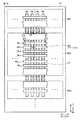
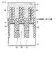
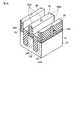
図2は、参考例に関わるNAND型フラッシュメモリのメモリセルアレイのレイアウトを示している。図3は、図2のIII−III線に沿う断面、図4は、図2のIV−IV線に沿う断面、図5は、図2のV−V線に沿う断面をそれぞれ示している。 FIG. 2 shows a layout of the memory cell array of the NAND flash memory according to the reference example. 3 shows a cross section taken along line III-III in FIG. 2, FIG. 4 shows a cross section taken along line IV-IV in FIG. 2, and FIG. 5 shows a cross section taken along line VV in FIG.
これらの図においては、説明を分かり易くするため、コントロールゲートよりも上の絶縁層及び導電層(ビット線、金属線など)を省略する。 In these drawings, the insulating layer and the conductive layer (bit line, metal line, etc.) above the control gate are omitted for easy understanding.
メモリセルアレイ11は、図1のメモリセルアレイ11に相当し、複数のブロックBK1,BK2,BK3,・・・から構成される。 The
各々のブロックは、ロウ方向に配置される複数のセルユニットを有する。複数のセルユニットの各々は、直列接続された複数のメモリセルからなるNANDストリング21と、その両端に1つずつ接続される2つのセレクトゲートトランジスタとから構成される。 Each block has a plurality of cell units arranged in the row direction. Each of the plurality of cell units includes a
半導体基板31内には、STI(shallow trench isolation)構造の素子分離絶縁層32が配置される。素子分離絶縁層32は、カラム方向に長いストライプ状に形成され、その間の領域は、アクティブ領域AAとなる。アクティブ領域AAには、セルユニットが配置される。 An element
メモリセルMCは、半導体基板31の表面領域に形成されるソース/ドレイン拡散層38と、ソース/ドレイン拡散層38間のチャネル領域上にトンネル酸化膜33を介して配置されるフローティングゲート34,35と、フローティングゲート34,35上にIPD(inter-poly dielectric)層36を介して配置されるコントロールゲート37とから構成される。 The memory cell MC includes a source /
選択ゲートトランジスタSTは、半導体基板31の表面領域に形成されるソース/ドレイン拡散層38と、ソース/ドレイン拡散層38間のチャネル領域上にゲート酸化膜39を介して配置されるゲート電極34’,35’,37’とから構成される。 The selection gate transistor ST includes a source /
ゲート電極34’,35’は、フローティングゲート34,35と同じ材料、例えば、導電性ポリシリコンから構成され、ゲート電極37’は、コントロールゲート37と同じ材料、例えば、導電性ポリシリコンとシリサイドとのスタック構造から構成される。絶縁層36’は、IPD層36と同じ構造、例えば、ONO(oxide-nitride-oxide)構造を有する。 The
ここで、フローティングゲート34は、素子分離絶縁層32の間のスペースに配置される。フローティングゲート35は、図3に示すように、フローティングゲート34上に配置され、NANDストリング21が延びる方向(カラム方向)における幅がフローティングゲート34のそれよりも狭い。 Here, the floating
その結果、フローティングゲート34,35のカラム方向の断面形状は、全体として凸形となり、メモリセルMCの微細化とカップリング比の増大を両立できる。 As a result, the cross-sectional shape in the column direction of the floating
一方、フローティングゲート35は、図4に示すように、コントロールゲート37が延びる方向(ロウ方向)における幅がフローティングゲート34のそれと同じである。 On the other hand, the floating
この場合、素子分離絶縁層32の幅を広げることにより、カップリング比を低下させずに、2つのメモリセルMCのフローティングゲート34,35の間に生じる寄生容量(セル間干渉)を小さくでき、メモリセルの閾値変動によるセル特性の劣化を防止できる。 In this case, by increasing the width of the element
しかし、メモリセルアレイ11の面積を一定とすると、素子分離絶縁層32の幅を広げるということは、アクティブ領域AAの幅を狭くすることを意味する。アクティブ領域の幅が狭くなると、メモリセルMCのチャネル幅が狭くなるため、メモリセルMCの電流駆動力が低下する。 However, when the area of the
そこで、特許文献1に開示される技術を用い、例えば、図4において、コントロールゲート37が延びる方向(ロウ方向)におけるフローティングゲート35の幅を、フローティングゲート34のそれよりも狭くすることも可能である。 Therefore, using the technique disclosed in
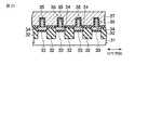
この場合、フローティングゲート34,35のロウ方向の断面は、図6に示すように、全体として凸形となる。 In this case, the cross section in the row direction of the floating
しかし、図6から明らかなように、フローティングゲート34,35のロウ方向の断面を凸形にするということは、素子分離絶縁層32の幅を狭めることを意味する。つまり、互いに隣接する2つのメモリセルMCについて、凸形の下部、即ち、フローティングゲート34の間のスペースが狭くなる結果、両メモリセルMCの寄生容量が増大し、セル特性の劣化が生じる。 However, as is apparent from FIG. 6, making the cross section in the row direction of the floating
これは、特に、IPD層36に、酸化シリコンよりも高い誘電率を持つ高誘電体(例えば、窒化シリコン)又はこれを含む複数の材料からなるスタック構造を使用する場合に顕著となる。 This is particularly noticeable when the
即ち、製造プロセス上、素子分離絶縁層32の上面は、フローティングゲート34の上面よりも低くなるのが一般的である。このため、フローティングゲート34,35が最も近接する領域(フローティングゲート34の間)に高誘電体が配置されると、セル間干渉効果が増長される。 In other words, the upper surface of the element
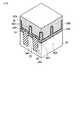
(3) 第1実施の形態
図7は、第1実施の形態に関わるNAND型フラッシュメモリのメモリセルアレイのレイアウトを示している。図8は、図7のVIII−VIII線に沿う断面、図9は、図7のIX−IX線に沿う断面、図10は、図7のX−X線に沿う断面をそれぞれ示している。(3) First embodiment
FIG. 7 shows a layout of the memory cell array of the NAND flash memory according to the first embodiment. 8 shows a cross section taken along line VIII-VIII in FIG. 7, FIG. 9 shows a cross section taken along line IX-IX in FIG. 7, and FIG. 10 shows a cross section taken along line XX in FIG.
これらの図においては、説明を分かり易くするため、コントロールゲートよりも上の絶縁層及び導電層(ビット線、金属線など)を省略する。 In these drawings, the insulating layer and the conductive layer (bit line, metal line, etc.) above the control gate are omitted for easy understanding.
メモリセルアレイ11は、図1のメモリセルアレイ11に相当し、複数のブロックBK1,BK2,BK3,・・・から構成される。 The
各々のブロックは、ロウ方向に配置される複数のセルユニットを有する。複数のセルユニットの各々は、直列接続された複数のメモリセルからなるNANDストリング21と、その両端に1つずつ接続される2つのセレクトゲートトランジスタとから構成される。 Each block has a plurality of cell units arranged in the row direction. Each of the plurality of cell units includes a
半導体基板31内には、STI構造の素子分離絶縁層32が配置される。素子分離絶縁層32は、カラム方向に長いストライプ状に形成され、その間の領域は、アクティブ領域AAとなる。アクティブ領域AAには、セルユニットが配置される。 An element
メモリセルMCは、半導体基板31の表面領域に形成されるソース/ドレイン拡散層38と、ソース/ドレイン拡散層38間のチャネル領域上にトンネル酸化膜33を介して配置されるフローティングゲート34,35と、フローティングゲート34,35上にIPD層36を介して配置されるコントロールゲート37とから構成される。 The memory cell MC includes a source /
選択ゲートトランジスタSTは、半導体基板31の表面領域に形成されるソース/ドレイン拡散層38と、ソース/ドレイン拡散層38間のチャネル領域上にゲート酸化膜39を介して配置されるゲート電極34’,35’,37’とから構成される。 The selection gate transistor ST includes a source /
ゲート電極34’,35’は、フローティングゲート34,35と同じ材料、例えば、導電性ポリシリコンから構成され、ゲート電極37’は、コントロールゲート37と同じ材料、例えば、導電性ポリシリコンとシリサイドとのスタック構造から構成される。絶縁層36’は、IPD層36と同じ構造、例えば、ONO構造を有する。 The
第1実施の形態では、フローティングゲート34が素子分離絶縁層32の間のスペースに配置される。フローティングゲート35は、フローティングゲート34上に配置され、カラム方向及びロウ方向における幅がフローティングゲート34のそれよりも狭い。 In the first embodiment, the floating
ここで、第1実施の形態が参考例と異なる点は、カラム方向とロウ方向の両方向について、それぞれフローティングゲート35の幅がフローティングゲート34のそれよりも狭い点にある。言い換えると、フローティングゲート35の全ての方向における幅が、フローティングゲート34の全ての方向における幅よりも狭いことになる。 Here, the first embodiment is different from the reference example in that the width of the floating
その結果、フローティングゲート34,35のカラム方向及びロウ方向の断面形状は、それぞれ凸形となり、参考例に比べ、さらなるメモリセルMCの微細化とカップリング比の増大を図ることができる。 As a result, the cross-sectional shapes in the column direction and the row direction of the floating
また、第1実施の形態では、素子分離絶縁層32の上面がフローティングゲート34の上面よりも低い位置に存在する。その結果、IPD層36が、互いに隣接する2つのメモリセルMCのフローティングゲート34の間にも配置される。 In the first embodiment, the upper surface of the element
しかし、第1実施の形態が参考例と異なる点は、フローティングゲート34の間に生じる寄生容量(セル間干渉)を小さくするために、フローティングゲート34の間のスペースには、1種類の絶縁体が満たされる点にある。 However, the first embodiment is different from the reference example in that one type of insulator is provided in the space between the floating
1種類の絶縁体とは、概要で定義したように、材料が同じであることを意味する。従って、本例の場合、フローティングゲート34の間には、素子分離絶縁層32とIPD層36とが配置されるため、IPD層36は、少なくとも、素子分離絶縁層32を構成する材料と同じ材料を含んでいる必要がある。 One type of insulator means that the materials are the same as defined in the overview. Therefore, in the case of this example, since the element
例えば、素子分離絶縁層32が酸化シリコン(SiO2)から構成される場合、IPD層36は、ONO構造、ONON構造のように、酸化シリコン(Oxide)を含む構造とする。For example, when the element
そして、重要な点は、例えば、図11に示すように、フローティングゲート34の間には、酸化シリコン(Oxide)が自己整合的に満たされる点にある。 An important point is that, for example, as shown in FIG. 11, silicon oxide (Oxide) is filled between the floating
また、フローティングゲート35の間のスペースには、フローティングゲート34の間の1種類の絶縁体の誘電率よりも高い誘電率を持つ誘電体を介してコントロールゲート37が配置される。 A
この誘電体は、例えば、IPD層36が、ONO構造又はONON構造の場合には、窒化シリコン(Nitride)である。 This dielectric is, for example, silicon nitride (Nitride) when the
このように、フローティングゲート34,35を凸形とし、フローティングゲート34,35が最も近接する領域に低い誘電率を持つ1種類の絶縁体を満たし、その他の領域に高い誘電率を持つ誘電体を配置することで、メモリセルMCが微細化されても、セル干渉効果による閾値変動なく、カップリング比を向上させることができる。 As described above, the floating
(4) 第2実施の形態
図12は、第2実施の形態に関わるNAND型フラッシュメモリのメモリセルアレイのレイアウトを示している。図13は、図12のXIII−XIII線に沿う断面、図14は、図12のXIV−XIV線に沿う断面、図15は、図12のXV−XV線に沿う断面をそれぞれ示している。(4) Second embodiment
FIG. 12 shows a layout of the memory cell array of the NAND flash memory according to the second embodiment. 13 shows a cross section taken along line XIII-XIII in FIG. 12, FIG. 14 shows a cross section taken along line XIV-XIV in FIG. 12, and FIG. 15 shows a cross section taken along line XV-XV in FIG.
これらの図においては、第1実施の形態と同様に、コントロールゲートよりも上の絶縁層及び導電層を省略する。また、メモリセルアレイ11の構造については、第1実施の形態と同じであるため、その説明を省略する。 In these drawings, the insulating layer and the conductive layer above the control gate are omitted as in the first embodiment. Further, since the structure of the
半導体基板31内には、STI構造の素子分離絶縁層32が配置される。素子分離絶縁層32は、カラム方向に長いストライプ状に形成され、その間の領域は、アクティブ領域AAとなる。アクティブ領域AAには、セルユニットが配置される。 An element
メモリセルMCは、半導体基板31の表面領域に形成されるソース/ドレイン拡散層38と、ソース/ドレイン拡散層38間のチャネル領域上にトンネル酸化膜33を介して配置されるフローティングゲート34,35と、フローティングゲート34,35上にIPD層36を介して配置されるコントロールゲート37とから構成される。 The memory cell MC includes a source /
選択ゲートトランジスタSTは、半導体基板31の表面領域に形成されるソース/ドレイン拡散層38と、ソース/ドレイン拡散層38間のチャネル領域上にゲート酸化膜39を介して配置されるゲート電極34’,35’,37’とから構成される。 The selection gate transistor ST includes a source /
ゲート電極34’,35’は、フローティングゲート34,35と同じ材料、例えば、導電性ポリシリコンから構成され、ゲート電極37’は、コントロールゲート37と同じ材料、例えば、導電性ポリシリコンとシリサイドとのスタック構造から構成される。絶縁層36’は、IPD層36と同じ構造、例えば、ONO構造を有する。 The
第2実施の形態では、フローティングゲート34が素子分離絶縁層32の間のスペースに配置される。また、フローティングゲート35は、フローティングゲート34上に配置され、カラム方向及びロウ方向の両方向における幅がフローティングゲート34のそれよりも狭いため、第1実施の形態と同様に、メモリセルMCの微細化とカップリング比の増大を図ることができる。 In the second embodiment, the floating
ここで、第2実施の形態が第1実施の形態と異なる点は、素子分離絶縁層32の上面がフローティングゲート34の上面と同じ位置に存在する点にある。 Here, the second embodiment is different from the first embodiment in that the upper surface of the element
この場合、フローティングゲート34の間のスペースには、素子分離絶縁層32のみが満たされるため、結果として、フローティングゲート34の間のスペースには、1種類の絶縁体が満たされる。 In this case, since the space between the floating
また、フローティングゲート35の間のスペースには、フローティングゲート34の間の1種類の絶縁体の誘電率よりも高い誘電率を持つ誘電体を介してコントロールゲート37が配置される。 A
従って、第2実施の形態によれば、第1実施の形態と同様に、メモリセルMCが微細化されても、セル干渉効果による閾値変動なく、カップリング比を向上させることができる。 Therefore, according to the second embodiment, as in the first embodiment, even if the memory cell MC is miniaturized, the coupling ratio can be improved without threshold fluctuation due to the cell interference effect.
また、第2の実施の形態では、素子分離絶縁層32の上面とフローティングゲート34の上面とが一致するため、IPD層36の構造に制限を受けない。 In the second embodiment, since the upper surface of the element
例えば、IPD層36は、図16に示すように、ONO構造を有していてもよいし、図17に示すように、NONO構造を有していてもよい。また、IPD層36は、図18に示すように、単層の高誘電体から構成されていてもよい。 For example, the
さらに、IPD層36は、ON構造、ONON構造、NON構造、NONON構造のような、酸化シリコン(Oxide)と窒化シリコン(Nitride)のスタック構造であってもよい。 Further, the
また、IPD膜36は、NOAON(Aは、Al2O3)であってもよい。The
このように、第2実施の形態においても、フローティングゲート34,35を凸形とし、フローティングゲート34,35が最も近接する領域に低い誘電率を持つ1種類の絶縁体を満たし、その他の領域に高い誘電率を持つ誘電体を配置することで、第1実施の形態と同様の効果を得ることができる。 As described above, also in the second embodiment, the floating
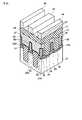
(5) 第3実施の形態
図19は、第3実施の形態に関わるNAND型フラッシュメモリのメモリセルアレイのレイアウトを示している。図20は、図19のXX−XX線に沿う断面、図21は、図19のXXI−XXI線に沿う断面、図22は、図19のXXII−XXII線に沿う断面をそれぞれ示している。(5) Third embodiment
FIG. 19 shows the layout of the memory cell array of the NAND flash memory according to the third embodiment. 20 shows a cross section taken along line XX-XX in FIG. 19, FIG. 21 shows a cross section taken along line XXI-XXI in FIG. 19, and FIG. 22 shows a cross section taken along line XXII-XXII in FIG.
これらの図においては、第1実施の形態と同様に、コントロールゲートよりも上の絶縁層及び導電層を省略する。また、メモリセルアレイ11の構造については、第1実施の形態と同じであるため、その説明を省略する。 In these drawings, the insulating layer and the conductive layer above the control gate are omitted as in the first embodiment. Further, since the structure of the
半導体基板31内には、STI構造の素子分離絶縁層32が配置される。素子分離絶縁層32は、カラム方向に長いストライプ状に形成され、その間の領域は、アクティブ領域AAとなる。アクティブ領域AAには、セルユニットが配置される。 An element
メモリセルMCは、半導体基板31の表面領域に形成されるソース/ドレイン拡散層38と、ソース/ドレイン拡散層38間のチャネル領域上にトンネル酸化膜33を介して配置されるフローティングゲート34,35と、フローティングゲート34,35上にIPD層36を介して配置されるコントロールゲート37とから構成される。 The memory cell MC includes a source /
選択ゲートトランジスタSTは、半導体基板31の表面領域に形成されるソース/ドレイン拡散層38と、ソース/ドレイン拡散層38間のチャネル領域上にゲート酸化膜39を介して配置されるゲート電極34’,35’,37’とから構成される。 The selection gate transistor ST includes a source /
ゲート電極34’,35’は、フローティングゲート34,35と同じ材料、例えば、導電性ポリシリコンから構成され、ゲート電極37’は、コントロールゲート37と同じ材料、例えば、導電性ポリシリコンとシリサイドとのスタック構造から構成される。絶縁層36’は、IPD層36と同じ構造、例えば、ONO構造を有する。 The
第3実施の形態では、フローティングゲート34がいわゆるガルウイング形を有している。即ち、フローティングゲート34は、ロウ方向における幅が素子分離絶縁層32のそれよりも広い。このような形状は、素子分離絶縁層32を形成した後に、フローティングゲート34のパターニングを行うことにより容易に得ることができる。 In the third embodiment, the floating
また、フローティングゲート35は、フローティングゲート34上に配置される。フローティングゲート35は、カラム方向及びロウ方向の両方向における幅がフローティングゲート34のそれよりも狭いため、第1実施の形態と同様に、メモリセルMCの微細化とカップリング比の増大を図ることができる。 The floating
ここで、第3実施の形態では、素子分離絶縁層32上に存在するフローティングゲート34の間のスペースが、互いに隣接する2つのメモリセルMCが最も近接する領域となる。 Here, in the third embodiment, a space between the floating
そこで、例えば、図23に示すように、素子分離絶縁層32上におけるフローティングゲート34の間のスペースに、IPD層36を構成する異なる誘電率の複数の材料のうち、最も低い誘電率を有する材料、即ち、素子分離絶縁層32を構成する材料と同じ材料 (例えば、酸化シリコン)を満たす。 Therefore, for example, as shown in FIG. 23, the material having the lowest dielectric constant among the plurality of materials having different dielectric constants constituting the
結果として、フローティングゲート34の間のスペースには、1種類の材料が満たされることになる。 As a result, the space between the floating
また、フローティングゲート35の間のスペースには、フローティングゲート34の間の1種類の絶縁体の誘電率よりも高い誘電率を持つ誘電体を介してコントロールゲート37が配置される。この誘電体は、例えば、IPD層36が、ONO構造の場合には、窒化シリコン(SixNy)である。 A
このように、第3実施の形態においても、フローティングゲート34,35を凸形とし、フローティングゲート34,35が最も近接する領域に低い誘電率を持つ1種類の絶縁体を満たし、その他の領域に高い誘電率を持つ誘電体を配置することで、メモリセルMCが微細化されても、セル干渉効果による閾値変動を少なく抑えて、カップリング比を向上させることができる。 As described above, also in the third embodiment, the floating
(6) 製造方法
本発明の例に関わる不揮発性半導体メモリの製造方法を説明する。(6) Manufacturing method
A method for manufacturing a nonvolatile semiconductor memory according to an example of the present invention will be described.
以下の製造方法は、凸形フローティングゲートの下部を形成した後に素子分離絶縁層を形成するプロセスに関し、上述の第1及び第2実施の形態の構造を作るのに適している。 The following manufacturing method relates to the process of forming the element isolation insulating layer after forming the lower part of the convex floating gate, and is suitable for making the structures of the first and second embodiments described above.
まず、図24に示すように、熱酸化法により、半導体基板31の表面にトンネル酸化膜33を形成する。続けて、CVD法により、トンネル酸化膜33上に導電性ポリシリコン膜34Aを形成する。また、CVD法により、導電性ポリシリコン膜34A上にスペーサとしての窒化シリコン膜41を形成し、さらに、窒化シリコン膜41上に酸化シリコン膜42を形成する。 First, as shown in FIG. 24, a
そして、フォトリソグラフィー(PEP: photo engraving process)により、レジストパターンを形成し、このレジストパターンをマスクにして酸化シリコン膜42をパターニングし、これをハードマスクする。この後、レジストパターンを除去する。 Then, a resist pattern is formed by photolithography (PEP: photo engraving process), the
次に、図25に示すように、酸化シリコン膜42をマスクにして、例えば、RIE(reactive ion etching)により、窒化シリコン膜41、導電性ポリシリコン膜34A、トンネル酸化膜33及び半導体基板31を順次エッチングする。その結果、ストライプ状のトレンチ43が形成される。 Next, as shown in FIG. 25, using the
次に、図26に示すように、CVD法により、トレンチ43を完全に満たす酸化シリコン膜を形成する。また、CMP(chemical mechanical polishing)法により、トレンチ43の外部に存在する酸化シリコン膜(図25の酸化シリコン膜42を含む)を除去し、トレンチ43内に素子分離絶縁層32を形成する。 Next, as shown in FIG. 26, a silicon oxide film that completely fills the
この後、素子分離絶縁層32をマスクにして、例えば、ホットリン酸により、窒化シリコン膜41をエッチングすると、図27に示すように、素子分離絶縁層32の上部が導電性ポリシリコン膜34Aの上面よりも上方に突出した構造が得られる。 Thereafter, when the
次に、図28に示すように、CVD法により、導電性ポリシリコン膜34A上及び素子分離絶縁層32上に窒化シリコン膜46を形成する。窒化シリコン膜46は、素子分離絶縁層32の上部の間のスペース45を完全に満たす厚さで形成される。 Next, as shown in FIG. 28, a
この後、CMP法により、素子分離絶縁層32の上面が露出するまで窒化シリコン膜46を研磨し、窒化シリコン膜46の上面を平坦化する。 Thereafter, the
また、フォトリソグラフィー(PEP)によりレジストパターンを形成し、このレジストパターンをマスクにして、窒化シリコン膜46に導電性ポリシリコン膜34Aに達する穴47を形成する。この後、レジストパターンを除去する。 Further, a resist pattern is formed by photolithography (PEP), and a
次に、図29に示すように、CVD法により、窒化シリコン膜46に形成された穴47を完全に満たす導電性ポリシリコン膜35Aを形成する。また、CMP法により、穴47の外部に存在する導電性ポリシリコン膜35Aを除去する。 Next, as shown in FIG. 29, a
この後、素子分離絶縁層32のみを選択的にエッチングすると、図30に示すように、素子分離絶縁層32の上面は、窒化シリコン膜46の上面よりも下となる位置まで後退する。 Thereafter, when only the element
ここで、素子分離絶縁層32の上面を後退させる量を調整することにより、第1又は第2実施の形態の構造を得ることができる。 Here, by adjusting the amount by which the upper surface of the element
尚、メモリセルのカップリング比を最大限に向上させるためには、素子分離絶縁層32の上面は、導電性ポリシリコン膜34Aの上面よりも下となる位置まで後退させるのが好ましい。 In order to maximize the coupling ratio of the memory cell, the upper surface of the element
続けて、例えば、ホットリン酸により、窒化シリコン膜46を除去する。 Subsequently, the
次に、図31に示すように、CVD法により、導電性ポリシリコン膜34A,35Aを覆うIPD層36を形成する。IPD層36は、例えば、ONO構造とする。また、CVD法により、IPD層36上に、導電性ポリシリコン膜37Aを形成する。 Next, as shown in FIG. 31, an
この後、フォトリソグラフィー(PEP)によりレジストパターンを形成し、このレジストパターンをマスクにして、導電性ポリシリコン膜37A、IPD層36、導電性ポリシリコン膜34A及びトンネル酸化膜33を順次エッチングする。 Thereafter, a resist pattern is formed by photolithography (PEP), and the
レジストパターンは、ストライプ状に形成され、図25のトレンチ43のストライプとは交差するように形成される。 The resist pattern is formed in a stripe shape so as to intersect with the stripe of the
その結果、図32に示すように、半導体基板31上に、トンネル酸化膜33を介して、フローティングゲート34,35、IPD層36及びコントロールゲート37がスタックされた構造が完成する。 As a result, as shown in FIG. 32, a structure in which the floating
ここで、フローティングゲート35は、柱状となっているため、その上面及び全ての側面は、コントロールゲート37により覆われる。 Here, since the floating
この後、コントロールゲート37をマスクにして、イオン注入法により、半導体基板11内に不純物を自己整合的に注入し、かつ、不純物を活性化させるためのアニールを行うと、ソース/ドレイン拡散層38が形成される。 Thereafter, when the
以上のプロセスにより、本発明の例に関わるメモリセルの構造が完成する。 Through the above process, the structure of the memory cell according to the example of the present invention is completed.
この後は、図33に示すように、CVD法により、コントロールゲート37を覆い、コントロールゲート37の間のスペースを満たす層間絶縁膜(例えば、SiO2)48を形成する。Thereafter, as shown in FIG. 33, an interlayer insulating film (for example, SiO2 ) 48 that covers the
また、層間絶縁膜48の上面をCMP法により平坦化した後、NANDストリングの一端となる領域にコンタクトホールを形成する。CVD法により導電性ポリシリコン膜を形成し、さらに、フォトリソグラフィー(PEP)により形成されたフォトレジストをマスクにして、RIE法により、導電性ポリシリコン膜をパターニングし、ビット線49を形成する。 Further, after planarizing the upper surface of the
尚、以上の製造方法は、第1及び第2実施の形態の構造を対象としているが、凸形フローティングゲートの下部の形成と素子分離絶縁層の形成の順序を入れ替えれば、第3実施の形態の構造にも適用が可能である。 The above manufacturing method is directed to the structures of the first and second embodiments. However, if the order of forming the lower portion of the convex floating gate and the formation of the element isolation insulating layer are interchanged, the third embodiment will be described. It can be applied to the structure of.
(7) その他
第1実施の形態に関し、IPD膜は、フローティングゲートに接触する部分に薄い高誘電率の誘電体が配置されていても、フローティングゲート間の大部分が低誘電率の誘電体に満たされていれば、本発明の効果を得ることができる。(7) Other
With respect to the first embodiment, the IPD film has a large portion between the floating gates filled with the dielectric having a low dielectric constant even if a thin dielectric having a high dielectric constant is disposed in the portion in contact with the floating gate. Thus, the effects of the present invention can be obtained.
例えば、IPD膜としては、NONON、NOAON(Aは、Al2O3)であってもよいが、この場合、フローティングゲート間の大部分は、O(oxide)により満たされ、フローティングゲート間においては、N(nitride)は、IPD膜とフローティングゲートとの界面にのみ存在する形にするのが好ましい。For example, the IPD film may be NONON or NOAON (A is Al2 O3 ). In this case, most of the space between the floating gates is filled with O (oxide). , N (nitride) is preferably present only at the interface between the IPD film and the floating gate.
上述の実施の形態は、NAND型フラッシュメモリについて説明したが、本発明の例は、フローティングゲートとコントロールゲートとを持つスタックゲート構造のメモリセルを備えた不揮発性半導体メモリ全般に適用できる。 In the above-described embodiment, the NAND flash memory has been described. However, the example of the present invention can be applied to all nonvolatile semiconductor memories including memory cells having a stack gate structure having a floating gate and a control gate.
3. まとめ
本発明の例によれば、新規なデバイス構造により、セル間干渉効果による閾値変動なく、カップリング比を向上できる。3. Summary
According to the example of the present invention, the novel device structure can improve the coupling ratio without fluctuations in threshold due to the inter-cell interference effect.
本発明の例は、上述の実施の形態に限定されるものではなく、その要旨を逸脱しない範囲で、各構成要素を変形して具体化できる。また、上述の実施の形態に開示されている複数の構成要素の適宜な組み合せにより種々の発明を構成できる。例えば、上述の実施の形態に開示される全構成要素から幾つかの構成要素を削除してもよいし、異なる実施の形態の構成要素を適宜組み合わせてもよい。 The example of the present invention is not limited to the above-described embodiment, and can be embodied by modifying each component without departing from the scope of the invention. Various inventions can be configured by appropriately combining a plurality of constituent elements disclosed in the above-described embodiments. For example, some constituent elements may be deleted from all the constituent elements disclosed in the above-described embodiments, or constituent elements of different embodiments may be appropriately combined.
11: メモリセルアレイ、 12: データラッチ回路、 13: I/Oバッファ、 14: アドレスバッファ、 15: ロウデコーダ、 16: カラムデコーダ、 17: ドライバ、 18: 基板電圧制御回路、 19: 電圧発生回路、 20: 制御回路、 21: NANDストリング、 31: 半導体基板、 32: 素子分離絶縁層、 33: トンネル酸化膜、 34,35: フローティングゲート、 36: IPD層、 37: コントロールゲート、 38: ソース/ドレイン拡散層、 39: ゲート酸化膜、 WL1,WL2,・・・WLn: ワード線(コントロールゲート)、 MC: メモリセル、 ST: 選択ゲートトランジスタ、 AA: アクティブ領域。 DESCRIPTION OF SYMBOLS 11: Memory cell array, 12: Data latch circuit, 13: I / O buffer, 14: Address buffer, 15: Row decoder, 16: Column decoder, 17: Driver, 18: Substrate voltage control circuit, 19: Voltage generation circuit, 20: control circuit, 21: NAND string, 31: semiconductor substrate, 32: element isolation insulating layer, 33: tunnel oxide film, 34, 35: floating gate, 36: IPD layer, 37: control gate, 38: source / drain Diffusion layer, 39: gate oxide film, WL1, WL2,... WLn: word line (control gate), MC: memory cell, ST: selection gate transistor, AA: active region.
Claims (5)
Translated fromJapanese前記第1及び第2のメモリセルのフローティングゲートは、それぞれ、第1部分と、前記第1部分上に配置され、前記コントロールゲートが延びる方向における幅が前記第1部分のそれよりも狭い第2部分とから構成され、
前記第1部分は、ストライプ状の素子分離絶縁層の間に配置され、前記素子分離絶縁層の上面は、前記第1部分の上面よりも低い位置に存在し、
前記ゲート間絶縁層は、前記フローティングゲートの上面、側面及び前記素子分離絶縁層の上面に沿うように形成され、前記フローティングゲート上の第1層と、前記第1層上の第2層とを備え、前記第2層の誘電率は、前記第1層及び前記素子分離絶縁層の誘電率よりも高く、
前記第1及び第2メモリセルの前記第1部分の間の第1スペースには、前記素子分離絶縁層及び前記第1層が満たされ、前記第1及び第2メモリセルの前記第2部分の間の第2スペースには、前記第1及び第2層が配置される
ことを特徴とする不揮発性半導体メモリ。A stack gate structure including a floating gate, a control gate,and an inter-gate insulating layer therebetween, and includes first and second memory cellsadjacent in a direction in which the control gate extends ;
The floating gates of the first and second memory cells are respectively disposed on the first portion and the first portion, and a second width in the direction in which the control gate extends is narrower than that of the first portion. Consists of parts and
The first portion is disposed between stripe-shaped element isolation insulating layers, and the upper surface of the element isolation insulating layer exists at a positionlower than theupper surface of the first portion,
The intergate insulating layer is formed along an upper surface, a side surface of the floating gate, and an upper surface of the element isolation insulating layer, and includes a first layer on the floating gate and a second layer on the first layer. The dielectric constant of the second layer is higher than the dielectric constant of the first layer and the element isolation insulating layer,
Wherein the first and the first space betweenthe first portion of the second memory cell,the element isolation insulating layer and said first layer is filled,the second portion of the first and second memory cell The non-volatile semiconductor memory,wherein the first and second layers are disposed in a second spacetherebetween .
Priority Applications (5)
| Application Number | Priority Date | Filing Date | Title |
|---|---|---|---|
| JP2006119416AJP4762041B2 (en) | 2006-04-24 | 2006-04-24 | Nonvolatile semiconductor memory |
| US11/687,758US7982259B2 (en) | 2006-04-24 | 2007-03-19 | Nonvolatile semiconductor memory |
| KR1020070039372AKR100878088B1 (en) | 2006-04-24 | 2007-04-23 | Nonvolatile Semiconductor Memory |
| US13/007,258US8637915B2 (en) | 2006-04-24 | 2011-01-14 | Nonvolatile semiconductor memory |
| US13/430,153US8324679B2 (en) | 2006-04-24 | 2012-03-26 | Nonvolatile semiconductor memory |
Applications Claiming Priority (1)
| Application Number | Priority Date | Filing Date | Title |
|---|---|---|---|
| JP2006119416AJP4762041B2 (en) | 2006-04-24 | 2006-04-24 | Nonvolatile semiconductor memory |
Publications (2)
| Publication Number | Publication Date |
|---|---|
| JP2007294595A JP2007294595A (en) | 2007-11-08 |
| JP4762041B2true JP4762041B2 (en) | 2011-08-31 |
Family
ID=38764932
Family Applications (1)
| Application Number | Title | Priority Date | Filing Date |
|---|---|---|---|
| JP2006119416AExpired - Fee RelatedJP4762041B2 (en) | 2006-04-24 | 2006-04-24 | Nonvolatile semiconductor memory |
Country Status (3)
| Country | Link |
|---|---|
| US (3) | US7982259B2 (en) |
| JP (1) | JP4762041B2 (en) |
| KR (1) | KR100878088B1 (en) |
Families Citing this family (33)
| Publication number | Priority date | Publication date | Assignee | Title |
|---|---|---|---|---|
| JP4762041B2 (en)* | 2006-04-24 | 2011-08-31 | 株式会社東芝 | Nonvolatile semiconductor memory |
| JP4829015B2 (en) | 2006-06-20 | 2011-11-30 | 株式会社東芝 | Nonvolatile semiconductor memory device |
| US7667260B2 (en)* | 2006-08-09 | 2010-02-23 | Micron Technology, Inc. | Nanoscale floating gate and methods of formation |
| TW200908230A (en)* | 2007-08-13 | 2009-02-16 | Nanya Technology Corp | Non-volatile memory and manufacturing method thereof |
| US20090100659A1 (en)* | 2007-09-26 | 2009-04-23 | Radovan Soumar | Trailer wheel locking pin retractor |
| JP2009135373A (en)* | 2007-12-03 | 2009-06-18 | Toshiba Corp | Nonvolatile semiconductor memory device |
| JP5361328B2 (en) | 2008-10-27 | 2013-12-04 | 株式会社東芝 | Method for manufacturing nonvolatile semiconductor memory device |
| WO2010086067A1 (en)* | 2009-01-29 | 2010-08-05 | International Business Machines Corporation | Memory transistor with a non-planar floating gate and manufacturing method thereof |
| JP5570953B2 (en)* | 2010-11-18 | 2014-08-13 | 株式会社東芝 | Nonvolatile semiconductor memory device and method of manufacturing nonvolatile semiconductor memory device |
| TWI506768B (en)* | 2010-12-22 | 2015-11-01 | Powerchip Technology Corp | Non-volatile memory and method of manufacturing same |
| US9136128B2 (en) | 2011-08-31 | 2015-09-15 | Micron Technology, Inc. | Methods and apparatuses including memory cells with air gaps and other low dielectric constant materials |
| JP2013197191A (en)* | 2012-03-16 | 2013-09-30 | Toshiba Corp | Nonvolatile semiconductor memory device |
| US8946807B2 (en) | 2013-01-24 | 2015-02-03 | Micron Technology, Inc. | 3D memory |
| US9184175B2 (en) | 2013-03-15 | 2015-11-10 | Micron Technology, Inc. | Floating gate memory cells in vertical memory |
| US9064970B2 (en) | 2013-03-15 | 2015-06-23 | Micron Technology, Inc. | Memory including blocking dielectric in etch stop tier |
| US9276011B2 (en) | 2013-03-15 | 2016-03-01 | Micron Technology, Inc. | Cell pillar structures and integrated flows |
| US8921923B2 (en) | 2013-03-18 | 2014-12-30 | Kabushiki Kaisha Toshiba | Method for manufacturing semiconductor memory device and semiconductor memory device |
| US9183940B2 (en) | 2013-05-21 | 2015-11-10 | Aplus Flash Technology, Inc. | Low disturbance, power-consumption, and latency in NAND read and program-verify operations |
| US9263137B2 (en) | 2013-06-27 | 2016-02-16 | Aplus Flash Technology, Inc. | NAND array architecture for multiple simutaneous program and read |
| WO2015013689A2 (en) | 2013-07-25 | 2015-01-29 | Aplus Flash Technology, Inc. | Nand array hiarchical bl structures for multiple-wl and all -bl simultaneous erase, erase-verify, program, program-verify, and read operations |
| US9293205B2 (en) | 2013-09-14 | 2016-03-22 | Aplus Flash Technology, Inc | Multi-task concurrent/pipeline NAND operations on all planes |
| US9437604B2 (en) | 2013-11-01 | 2016-09-06 | Micron Technology, Inc. | Methods and apparatuses having strings of memory cells including a metal source |
| US9613704B2 (en) | 2013-12-25 | 2017-04-04 | Aplus Flash Technology, Inc | 2D/3D NAND memory array with bit-line hierarchical structure for multi-page concurrent SLC/MLC program and program-verify |
| JP2016009839A (en)* | 2014-06-26 | 2016-01-18 | 株式会社東芝 | Manufacturing method of semiconductor device |
| US9287280B2 (en)* | 2014-07-09 | 2016-03-15 | Taiwan Semiconductor Manufacturing Co., Ltd. | Method to improve memory cell erasure |
| US9659636B2 (en) | 2014-07-22 | 2017-05-23 | Peter Wung Lee | NAND memory array with BL-hierarchical structure for concurrent all-BL, all-threshold-state program, and alternative-WL program, odd/even read and verify operations |
| TWI555179B (en) | 2015-02-02 | 2016-10-21 | 力晶科技股份有限公司 | Isolation structure and manufacturing method thereof having non-volatile memory |
| US9558814B2 (en) | 2015-04-10 | 2017-01-31 | HGST Netherlands, B.V. | Hybrid analog and digital memory device |
| CN106298678A (en)* | 2016-08-22 | 2017-01-04 | 上海华力微电子有限公司 | A kind of method for improving of the control gate coefficient of coup |
| US10453855B2 (en) | 2017-08-11 | 2019-10-22 | Micron Technology, Inc. | Void formation in charge trap structures |
| US10680006B2 (en) | 2017-08-11 | 2020-06-09 | Micron Technology, Inc. | Charge trap structure with barrier to blocking region |
| US10446572B2 (en) | 2017-08-11 | 2019-10-15 | Micron Technology, Inc. | Void formation for charge trap structures |
| US10164009B1 (en) | 2017-08-11 | 2018-12-25 | Micron Technology, Inc. | Memory device including voids between control gates |
Family Cites Families (28)
| Publication number | Priority date | Publication date | Assignee | Title |
|---|---|---|---|---|
| KR100389918B1 (en)* | 2000-11-14 | 2003-07-04 | 삼성전자주식회사 | Highly integrated non-volatile memory cell array having high program speed |
| KR100421049B1 (en)* | 2001-09-28 | 2004-03-04 | 삼성전자주식회사 | Method for manufacturing semiconductor memory device |
| KR100436673B1 (en)* | 2001-05-28 | 2004-07-02 | 가부시끼가이샤 도시바 | Semiconductor device and manufacturing method thereof |
| JP2003023115A (en)* | 2001-07-06 | 2003-01-24 | Mitsubishi Electric Corp | Manufacturing method of nonvolatile semiconductor memory device and nonvolatile semiconductor memory device |
| JP2004022819A (en) | 2002-06-17 | 2004-01-22 | Toshiba Corp | Semiconductor device and manufacturing method thereof |
| US6908817B2 (en)* | 2002-10-09 | 2005-06-21 | Sandisk Corporation | Flash memory array with increased coupling between floating and control gates |
| JP3914142B2 (en) | 2002-11-29 | 2007-05-16 | 株式会社東芝 | Nonvolatile semiconductor memory device and manufacturing method thereof |
| JP2004214510A (en)* | 2003-01-07 | 2004-07-29 | Toshiba Corp | Nonvolatile semiconductor memory device and method of manufacturing the same |
| JP2004281662A (en) | 2003-03-14 | 2004-10-07 | Toshiba Corp | Semiconductor storage device and method of manufacturing the same |
| US7105406B2 (en)* | 2003-06-20 | 2006-09-12 | Sandisk Corporation | Self aligned non-volatile memory cell and process for fabrication |
| US6992929B2 (en)* | 2004-03-17 | 2006-01-31 | Actrans System Incorporation, Usa | Self-aligned split-gate NAND flash memory and fabrication process |
| JP2005277035A (en)* | 2004-03-24 | 2005-10-06 | Renesas Technology Corp | Nonvolatile semiconductor memory device and manufacturing method thereof |
| JP4761747B2 (en)* | 2004-09-22 | 2011-08-31 | 株式会社東芝 | Semiconductor device |
| US7279385B2 (en)* | 2004-12-20 | 2007-10-09 | Macronix International Co., Ltd. | Flash memory device and manufacturing method thereof |
| KR100609587B1 (en)* | 2004-12-30 | 2006-08-08 | 매그나칩 반도체 유한회사 | Manufacturing method of nonvolatile memory device |
| JP2006344746A (en)* | 2005-06-08 | 2006-12-21 | Toshiba Corp | Nonvolatile semiconductor memory device and manufacturing method thereof |
| US7687860B2 (en)* | 2005-06-24 | 2010-03-30 | Samsung Electronics Co., Ltd. | Semiconductor device including impurity regions having different cross-sectional shapes |
| JP2007036260A (en)* | 2005-07-27 | 2007-02-08 | Samsung Electronics Co Ltd | Nonvolatile memory device and manufacturing method thereof |
| KR100781563B1 (en)* | 2005-08-31 | 2007-12-03 | 삼성전자주식회사 | Non-volatile memory device and manufacturing method thereof. |
| KR100672132B1 (en) | 2005-09-13 | 2007-01-19 | 주식회사 하이닉스반도체 | Manufacturing method of semiconductor device |
| KR100684888B1 (en)* | 2005-11-11 | 2007-02-20 | 삼성전자주식회사 | Nonvolatile Memory Device and Manufacturing Method Thereof |
| US7436703B2 (en)* | 2005-12-27 | 2008-10-14 | Sandisk Corporation | Active boosting to minimize capacitive coupling effect between adjacent gates of flash memory devices |
| JP4762041B2 (en)* | 2006-04-24 | 2011-08-31 | 株式会社東芝 | Nonvolatile semiconductor memory |
| US7667260B2 (en)* | 2006-08-09 | 2010-02-23 | Micron Technology, Inc. | Nanoscale floating gate and methods of formation |
| US20080074920A1 (en)* | 2006-09-21 | 2008-03-27 | Henry Chien | Nonvolatile Memory with Reduced Coupling Between Floating Gates |
| JP2008118007A (en)* | 2006-11-07 | 2008-05-22 | Toshiba Corp | Nonvolatile semiconductor memory device and manufacturing method thereof |
| US7867843B2 (en)* | 2006-12-22 | 2011-01-11 | Intel Corporation | Gate structures for flash memory and methods of making same |
| JP2012033766A (en) | 2010-07-30 | 2012-02-16 | Toshiba Corp | Semiconductor storage device and manufacturing method of the same |
- 2006
- 2006-04-24JPJP2006119416Apatent/JP4762041B2/ennot_activeExpired - Fee Related
- 2007
- 2007-03-19USUS11/687,758patent/US7982259B2/ennot_activeExpired - Fee Related
- 2007-04-23KRKR1020070039372Apatent/KR100878088B1/ennot_activeExpired - Fee Related
- 2011
- 2011-01-14USUS13/007,258patent/US8637915B2/ennot_activeExpired - Fee Related
- 2012
- 2012-03-26USUS13/430,153patent/US8324679B2/ennot_activeExpired - Fee Related
Also Published As
| Publication number | Publication date |
|---|---|
| US20120181598A1 (en) | 2012-07-19 |
| US7982259B2 (en) | 2011-07-19 |
| JP2007294595A (en) | 2007-11-08 |
| US8324679B2 (en) | 2012-12-04 |
| US20110108905A1 (en) | 2011-05-12 |
| KR100878088B1 (en) | 2009-01-14 |
| KR20070104855A (en) | 2007-10-29 |
| US8637915B2 (en) | 2014-01-28 |
| US20080012061A1 (en) | 2008-01-17 |
Similar Documents
| Publication | Publication Date | Title |
|---|---|---|
| JP4762041B2 (en) | Nonvolatile semiconductor memory | |
| JP3583579B2 (en) | Nonvolatile semiconductor memory device and method of manufacturing the same | |
| US7795080B2 (en) | Methods of forming integrated circuit devices using composite spacer structures | |
| US7683422B2 (en) | Non-volatile memory devices with wraparound-shaped floating gate electrodes and methods of forming same | |
| JP2007299975A (en) | Semiconductor device, and its manufacturing method | |
| JP2008130676A (en) | Nonvolatile semiconductor memory device | |
| US20070002622A1 (en) | Nonvolatile semiconductor memory device including memory cell units each having a given number of memory cell transistors | |
| US7636256B2 (en) | Semiconductor memory device | |
| US20070257307A1 (en) | NAND non-volatile two-bit memory and fabrication method | |
| JP4901452B2 (en) | Nonvolatile semiconductor memory | |
| US7355241B2 (en) | Non-volatile memory | |
| US20070228455A1 (en) | Semiconductor device and manufacturing method thereof | |
| US8093647B2 (en) | Nonvolatile semiconductor memory having transistor with a diffusion blocking layer between the lower gate and fully silicided upper gate | |
| US7358129B2 (en) | Nonvolatile semiconductor memory device and a method of the same | |
| KR100706249B1 (en) | Non-volatile memory device having a fin type active region and its manufacturing method | |
| JP2006504261A (en) | Flash EEPROM unit cell and memory array structure including the same | |
| JP4117998B2 (en) | Nonvolatile semiconductor memory device, reading, writing and erasing methods thereof, and manufacturing method thereof | |
| JP2007142468A (en) | Semiconductor device | |
| US7541638B2 (en) | Symmetrical and self-aligned non-volatile memory structure | |
| US7842998B2 (en) | Nonvolatile semiconductor memory device and method for manufacturing the same | |
| JP2010258032A (en) | Nonvolatile semiconductor memory device and manufacturing method thereof | |
| US7671400B2 (en) | Semiconductor memory device including double spacers on sidewall of flating gate, electronic device including the same | |
| JP4480541B2 (en) | Nonvolatile semiconductor memory device | |
| JP2007012739A (en) | Nonvolatile semiconductor memory device and its manufacturing method | |
| JP2006173452A (en) | Nonvolatile semiconductor memory, and manufacturing method thereof |
Legal Events
| Date | Code | Title | Description |
|---|---|---|---|
| A621 | Written request for application examination | Free format text:JAPANESE INTERMEDIATE CODE: A621 Effective date:20090209 | |
| A977 | Report on retrieval | Free format text:JAPANESE INTERMEDIATE CODE: A971007 Effective date:20110126 | |
| A131 | Notification of reasons for refusal | Free format text:JAPANESE INTERMEDIATE CODE: A131 Effective date:20110201 | |
| A521 | Request for written amendment filed | Free format text:JAPANESE INTERMEDIATE CODE: A523 Effective date:20110330 | |
| A01 | Written decision to grant a patent or to grant a registration (utility model) | Free format text:JAPANESE INTERMEDIATE CODE: A01 Effective date:20110510 | |
| A61 | First payment of annual fees (during grant procedure) | Free format text:JAPANESE INTERMEDIATE CODE: A61 Effective date:20110607 | |
| FPAY | Renewal fee payment (event date is renewal date of database) | Free format text:PAYMENT UNTIL: 20140617 Year of fee payment:3 | |
| FPAY | Renewal fee payment (event date is renewal date of database) | Free format text:PAYMENT UNTIL: 20140617 Year of fee payment:3 | |
| LAPS | Cancellation because of no payment of annual fees |