JP4759917B2 - Thin film device manufacturing method, thin film device, and liquid crystal display device - Google Patents
Thin film device manufacturing method, thin film device, and liquid crystal display deviceDownload PDFInfo
- Publication number
- JP4759917B2 JP4759917B2JP2003417458AJP2003417458AJP4759917B2JP 4759917 B2JP4759917 B2JP 4759917B2JP 2003417458 AJP2003417458 AJP 2003417458AJP 2003417458 AJP2003417458 AJP 2003417458AJP 4759917 B2JP4759917 B2JP 4759917B2
- Authority
- JP
- Japan
- Prior art keywords
- substrate
- thin film
- layer
- film device
- liquid crystal
- Prior art date
- Legal status (The legal status is an assumption and is not a legal conclusion. Google has not performed a legal analysis and makes no representation as to the accuracy of the status listed.)
- Expired - Fee Related
Links
- 239000010409thin filmSubstances0.000titledescription130
- 238000004519manufacturing processMethods0.000titledescription61
- 239000004973liquid crystal related substanceSubstances0.000titledescription44
- 239000000758substrateSubstances0.000description204
- 239000010410layerSubstances0.000description173
- 239000010408filmSubstances0.000description57
- 238000000034methodMethods0.000description46
- 239000012790adhesive layerSubstances0.000description32
- 229910021420polycrystalline siliconInorganic materials0.000description28
- 229920005591polysiliconPolymers0.000description28
- KRHYYFGTRYWZRS-UHFFFAOYSA-NFluoraneChemical compoundFKRHYYFGTRYWZRS-UHFFFAOYSA-N0.000description27
- VYPSYNLAJGMNEJ-UHFFFAOYSA-Nsilicon dioxideInorganic materialsO=[Si]=OVYPSYNLAJGMNEJ-UHFFFAOYSA-N0.000description22
- 238000005530etchingMethods0.000description20
- 239000004033plasticSubstances0.000description20
- 229920003023plasticPolymers0.000description20
- 229910021417amorphous siliconInorganic materials0.000description18
- 239000011521glassSubstances0.000description17
- 239000011241protective layerSubstances0.000description17
- 229910052814silicon oxideInorganic materials0.000description17
- 229910004298SiO 2Inorganic materials0.000description16
- 230000001681protective effectEffects0.000description15
- ZOKXTWBITQBERF-UHFFFAOYSA-NMolybdenumChemical compound[Mo]ZOKXTWBITQBERF-UHFFFAOYSA-N0.000description14
- 229910052750molybdenumInorganic materials0.000description14
- 239000011733molybdenumSubstances0.000description14
- 238000004544sputter depositionMethods0.000description13
- 238000002161passivationMethods0.000description10
- 238000005268plasma chemical vapour depositionMethods0.000description10
- 238000005516engineering processMethods0.000description9
- 239000000853adhesiveSubstances0.000description8
- 230000001070adhesive effectEffects0.000description8
- 229910052581Si3N4Inorganic materials0.000description7
- HQVNEWCFYHHQES-UHFFFAOYSA-Nsilicon nitrideChemical compoundN12[Si]34N5[Si]62N3[Si]51N64HQVNEWCFYHHQES-UHFFFAOYSA-N0.000description7
- 239000004831Hot glueSubstances0.000description6
- 230000015572biosynthetic processEffects0.000description6
- 238000002347injectionMethods0.000description6
- 239000007924injectionSubstances0.000description6
- 238000005498polishingMethods0.000description6
- 239000011112polyethylene naphthalateSubstances0.000description6
- -1polyethylene terephthalatePolymers0.000description6
- 239000011347resinSubstances0.000description6
- 229920005989resinPolymers0.000description6
- AMGQUBHHOARCQH-UHFFFAOYSA-Nindium;oxotinChemical compound[In].[Sn]=OAMGQUBHHOARCQH-UHFFFAOYSA-N0.000description5
- 238000000059patterningMethods0.000description5
- 229920003207poly(ethylene-2,6-naphthalate)Polymers0.000description5
- 239000010453quartzSubstances0.000description5
- 238000005401electroluminescenceMethods0.000description4
- 239000011159matrix materialSubstances0.000description4
- 229910052751metalInorganic materials0.000description4
- 239000002184metalSubstances0.000description4
- 238000000206photolithographyMethods0.000description4
- 238000004528spin coatingMethods0.000description4
- 239000000126substanceSubstances0.000description4
- QTBSBXVTEAMEQO-UHFFFAOYSA-NAcetic acidChemical compoundCC(O)=OQTBSBXVTEAMEQO-UHFFFAOYSA-N0.000description3
- LFQSCWFLJHTTHZ-UHFFFAOYSA-NEthanolChemical compoundCCOLFQSCWFLJHTTHZ-UHFFFAOYSA-N0.000description3
- 239000002253acidSubstances0.000description3
- 229910052782aluminiumInorganic materials0.000description3
- XAGFODPZIPBFFR-UHFFFAOYSA-NaluminiumChemical compound[Al]XAGFODPZIPBFFR-UHFFFAOYSA-N0.000description3
- 239000003795chemical substances by applicationSubstances0.000description3
- 229910021419crystalline siliconInorganic materials0.000description3
- 238000000151depositionMethods0.000description3
- 230000005525hole transportEffects0.000description3
- 229910052698phosphorusInorganic materials0.000description3
- 239000011574phosphorusSubstances0.000description3
- 229920000139polyethylene terephthalatePolymers0.000description3
- 239000005020polyethylene terephthalateSubstances0.000description3
- 238000009751slip formingMethods0.000description3
- STTGYIUESPWXOW-UHFFFAOYSA-N2,9-dimethyl-4,7-diphenyl-1,10-phenanthrolineChemical groupC=12C=CC3=C(C=4C=CC=CC=4)C=C(C)N=C3C2=NC(C)=CC=1C1=CC=CC=C1STTGYIUESPWXOW-UHFFFAOYSA-N0.000description2
- 229910000838Al alloyInorganic materials0.000description2
- 229920002799BoPETPolymers0.000description2
- UFHFLCQGNIYNRP-UHFFFAOYSA-NHydrogenChemical compound[H][H]UFHFLCQGNIYNRP-UHFFFAOYSA-N0.000description2
- NBIIXXVUZAFLBC-UHFFFAOYSA-NPhosphoric acidChemical compoundOP(O)(O)=ONBIIXXVUZAFLBC-UHFFFAOYSA-N0.000description2
- 239000004372Polyvinyl alcoholSubstances0.000description2
- 230000000903blocking effectEffects0.000description2
- 239000011651chromiumSubstances0.000description2
- 239000003086colorantSubstances0.000description2
- 239000004020conductorSubstances0.000description2
- 238000005520cutting processMethods0.000description2
- 230000007423decreaseEffects0.000description2
- 229910052739hydrogenInorganic materials0.000description2
- 239000001257hydrogenSubstances0.000description2
- 230000001678irradiating effectEffects0.000description2
- 238000001459lithographyMethods0.000description2
- 239000000463materialSubstances0.000description2
- 239000012044organic layerSubstances0.000description2
- 229920001721polyimidePolymers0.000description2
- 229920002451polyvinyl alcoholPolymers0.000description2
- 239000003870refractory metalSubstances0.000description2
- 239000000565sealantSubstances0.000description2
- 238000007789sealingMethods0.000description2
- 125000006850spacer groupChemical group0.000description2
- 239000010935stainless steelSubstances0.000description2
- 229910001220stainless steelInorganic materials0.000description2
- TVIVIEFSHFOWTE-UHFFFAOYSA-Ktri(quinolin-8-yloxy)alumaneChemical compound[Al+3].C1=CN=C2C([O-])=CC=CC2=C1.C1=CN=C2C([O-])=CC=CC2=C1.C1=CN=C2C([O-])=CC=CC2=C1TVIVIEFSHFOWTE-UHFFFAOYSA-K0.000description2
- 238000007740vapor depositionMethods0.000description2
- ZCYVEMRRCGMTRW-UHFFFAOYSA-N7553-56-2Chemical compound[I]ZCYVEMRRCGMTRW-UHFFFAOYSA-N0.000description1
- VYZAMTAEIAYCRO-UHFFFAOYSA-NChromiumChemical compound[Cr]VYZAMTAEIAYCRO-UHFFFAOYSA-N0.000description1
- 239000004593EpoxySubstances0.000description1
- GRYLNZFGIOXLOG-UHFFFAOYSA-NNitric acidChemical compoundO[N+]([O-])=OGRYLNZFGIOXLOG-UHFFFAOYSA-N0.000description1
- XUIMIQQOPSSXEZ-UHFFFAOYSA-NSiliconChemical compound[Si]XUIMIQQOPSSXEZ-UHFFFAOYSA-N0.000description1
- BQCADISMDOOEFD-UHFFFAOYSA-NSilverChemical compound[Ag]BQCADISMDOOEFD-UHFFFAOYSA-N0.000description1
- 229910006404SnO 2Inorganic materials0.000description1
- NIXOWILDQLNWCW-UHFFFAOYSA-Nacrylic acid groupChemical groupC(C=C)(=O)ONIXOWILDQLNWCW-UHFFFAOYSA-N0.000description1
- 229910000147aluminium phosphateInorganic materials0.000description1
- 238000001505atmospheric-pressure chemical vapour depositionMethods0.000description1
- 230000005587bubblingEffects0.000description1
- 238000005229chemical vapour depositionMethods0.000description1
- 229910052804chromiumInorganic materials0.000description1
- 239000011247coating layerSubstances0.000description1
- 238000000576coating methodMethods0.000description1
- 239000000470constituentSubstances0.000description1
- 238000003618dip coatingMethods0.000description1
- 230000000694effectsEffects0.000description1
- 238000001810electrochemical catalytic reformingMethods0.000description1
- 238000010438heat treatmentMethods0.000description1
- RBTKNAXYKSUFRK-UHFFFAOYSA-Nheliogen blueChemical compound[Cu].[N-]1C2=C(C=CC=C3)C3=C1N=C([N-]1)C3=CC=CC=C3C1=NC([N-]1)=C(C=CC=C3)C3=C1N=C([N-]1)C3=CC=CC=C3C1=N2RBTKNAXYKSUFRK-UHFFFAOYSA-N0.000description1
- 239000011630iodineSubstances0.000description1
- 229910052740iodineInorganic materials0.000description1
- 238000004518low pressure chemical vapour depositionMethods0.000description1
- 239000000113methacrylic resinSubstances0.000description1
- 125000000896monocarboxylic acid groupChemical group0.000description1
- QPJSUIGXIBEQAC-UHFFFAOYSA-Nn-(2,4-dichloro-5-propan-2-yloxyphenyl)acetamideChemical compoundCC(C)OC1=CC(NC(C)=O)=C(Cl)C=C1ClQPJSUIGXIBEQAC-UHFFFAOYSA-N0.000description1
- 229910017604nitric acidInorganic materials0.000description1
- TWNQGVIAIRXVLR-UHFFFAOYSA-Noxo(oxoalumanyloxy)alumaneChemical compoundO=[Al]O[Al]=OTWNQGVIAIRXVLR-UHFFFAOYSA-N0.000description1
- 229920003229poly(methyl methacrylate)Polymers0.000description1
- 238000000926separation methodMethods0.000description1
- 229910052710siliconInorganic materials0.000description1
- 239000010703siliconSubstances0.000description1
- 229910052709silverInorganic materials0.000description1
- 239000004332silverSubstances0.000description1
- 239000000243solutionSubstances0.000description1
- 238000005507sprayingMethods0.000description1
- 238000003756stirringMethods0.000description1
- 125000005504styryl groupChemical group0.000description1
Images


Landscapes
- Liquid Crystal (AREA)
- Thin Film Transistor (AREA)
- Electroluminescent Light Sources (AREA)
- Recrystallisation Techniques (AREA)
- Devices For Indicating Variable Information By Combining Individual Elements (AREA)
Description
Translated fromJapanese本発明は、耐熱性の高い製造基板上に作製した後に実使用基板上に転写することが容易な薄膜デバイスの製造方法、薄膜デバイス、およびその薄膜デバイスを用いた液晶表示装置に関するものである。The present invention relates a method of manufacturing a easy thin film device to be transferred practically substrate after forming the high manufacturing heat-resistant substrate, a thin film device, andthe liquid crystal displayequipment using the thin film device is there.
近年、薄膜デバイスは、使用機器の小型化の影響を受けて、薄型化、軽量化、堅牢化に対する要求を受けている。しかしながら、薄膜デバイスは、高温、真空という環境で作製されるために、製造に使われる基板に制限がある。例えば、薄膜トランジスタを用いた液晶表示装置では、1000℃の温度に耐える石英基板、500℃の温度に耐えるガラス基板が使われている。これらの基板の薄型化も検討されているが、石英基板、ガラス基板を用いる限り、基板の剛性が低下することを考慮して基板サイズを縮小せざるを得ず、それによって生産性が低下する。また、基板が薄くなれば堅牢さも急激に低下するため、実用上の問題点となる。このように、製造基板に要求されている性能と実際に使用する際に求められている性能とが異なる。また、薄型、軽量、堅牢化が可能なプラスチック基板上に直接、薄膜トランジスタを作製しようという試みもあるが、耐熱温度の点から困難さが高い。 In recent years, thin film devices have been required to be thinner, lighter, and more robust due to the downsizing of equipment used. However, since a thin film device is manufactured in an environment of high temperature and vacuum, there are limitations on the substrate used for manufacturing. For example, in a liquid crystal display device using a thin film transistor, a quartz substrate that can withstand a temperature of 1000 ° C. and a glass substrate that can withstand a temperature of 500 ° C. are used. Although thinning of these substrates is also under consideration, as long as quartz substrates and glass substrates are used, the substrate size must be reduced in consideration of the decrease in substrate rigidity, thereby reducing productivity. . In addition, as the substrate becomes thinner, the robustness rapidly decreases, which is a practical problem. As described above, the performance required for the manufacturing substrate is different from the performance required for actual use. In addition, there is an attempt to manufacture a thin film transistor directly on a thin, lightweight, and robust plastic substrate, but the difficulty is high in terms of heat-resistant temperature.
そこで、耐熱温度の高い製造基板上に形成した薄膜デバイスを実使用基板に転写する技術が検討されている。転写する方法としては、剥離層を設けてデバイス作製後に剥離層から剥離する方法(例えば、特許文献1参照。)や、エッチングによりガラス基板を除去してしまう方法(例えば、特許文献2参照。)などが検討されている。 Therefore, a technique for transferring a thin film device formed on a production substrate having a high heat-resistant temperature to an actual use substrate has been studied. As a transfer method, a peeling layer is provided and a device is peeled off after the device is manufactured (for example, see Patent Document 1), or a glass substrate is removed by etching (for example, see Patent Document 2). Etc. are being considered.
膨張係数の高い通常のプラスチック基板に転写を行うと、薄膜層もしくは部分的に残っているガラスと、プラスチック基板の膨張係数が違うため、転写後に加熱すると、反ってしまうという問題がある。また、反った状態でさらに温度を上げると、薄膜層もしくは部分的に残っているガラスにクラックが入って破壊してしまうこともある。膨張係数の低いプラスチックには、2軸延伸ポリエチレンテレフタレートのように、延伸させて前後膨張係数を下げているものがあるが、その場合複屈折を持っている。液晶表示装置に使用する場合、偏光板により偏光された光が複屈折を持つ基板を通ると、直線偏光が楕円偏光または円偏光となり、液晶表示装置として正しく機能しなくなる。そのため、膨張係数が小さくても複屈折を持つプラスチック基板は、液晶表示装置には使用できないという問題点がある。 When transfer is performed on a normal plastic substrate having a high expansion coefficient, the expansion coefficient of the plastic substrate is different from that of the thin film layer or partially remaining glass, so that there is a problem that the film is warped when heated after transfer. Further, if the temperature is further raised in a warped state, the thin film layer or partially remaining glass may crack and break. Some plastics having a low expansion coefficient, such as biaxially stretched polyethylene terephthalate, are drawn to lower the expansion coefficient in the front-rear direction. In this case, the plastic has birefringence. When used in a liquid crystal display device, when the light polarized by the polarizing plate passes through a substrate having birefringence, the linearly polarized light becomes elliptically polarized light or circularly polarized light and does not function correctly as a liquid crystal display device. Therefore, there is a problem that a plastic substrate having birefringence even if the expansion coefficient is small cannot be used for a liquid crystal display device.
本発明の薄膜デバイスの製造方法は、第1基板上にトランジスタを含む薄膜デバイス層を形成した後に薄膜デバイス層上に第1接着層を介してもしくは被覆層と第1接着層とを介して第2基板を接着する工程と、化学処理および機械的研磨処理および紫外線照射処理の少なくとも一つの処理を含む工程により第1基板を完全または部分的に分離または除去する工程と、薄膜デバイス層の第1基板が形成されていた側または部分的に残した第1基板に、第2接着層を介して偏光板としての第3基板を接着する工程と、第2基板を分離または除去する工程とを備えた薄膜デバイスの製造方法において、第3基板として、薄膜デバイス層側から順に、偏光子と、線膨張係数が20ppm/K以下であると共に複屈折を有する支持体とを有するものを用いるものである。Method of manufacturing a thin film device of the present invention, via the after formingthe thin film device layerincluding a transistor on the first substrate through a first adhesive layer onthe thin film device layer or coating layer and the first adhesive layer Te and bonding a second substrate, a chemical treatment and mechanical polishing treatment and the step of completely or partially separated or removedfirst substrateRi by the step of including at least one processing of the ultraviolet irradiationtreatment, a thin filmthe first substrate leaving the device layer first substrate side or partially has been formed, the separation or removal and bondinga thirdsubstrate as a polarizing plate through a second adhesivelayer, asecond substrate In the thin film device manufacturing method comprising the steps of: athird substrate having, in order from the thin film device layer side, a polarizer and a support having a linear expansion coefficient of 20 ppm / K or less and birefringence The It is those who are.
本発明の薄膜デバイスは、第1基板上にトランジスタを含む薄膜デバイス層を形成した後に薄膜デバイス層上に第1接着層を介してもしくは被覆層と第1接着層とを介して第2基板を接着する工程と、化学処理および機械的研磨処理および紫外線照射処理の少なくとも一つの処理を含む工程により第1基板を完全または部分的に分離または除去する工程と、薄膜デバイス層の第1基板が形成されていた側または部分的に残した第1基板に、第2接着層を介して偏光板としての第3基板を接着する工程と、第2基板を分離または除去する工程とにより製造される薄膜デバイスにおいて、第3基板が、薄膜デバイス層側から順に、偏光子と、線膨張係数が20ppm/K以下であると共に複屈折を有する支持体とを有するものである。Thin film device of the present invention, the via after formingthe thin film device layerincluding a transistor on the first substrate through a first adhesive layer onthe thin film device layer or the covering layer and the first adhesive layer 2 a step of bonding the substrate, the chemical treatment and mechanical polishing treatment and the step of completely or partially separated or removedfirst substrateRi by the step of including at least one processing of the ultraviolet irradiationtreatment, thethin film device layerthe first substrate leaving first the substrate side or in part been formed, a step of bondingthe thirdsubstrate as a polarizing plate through a second adhesivelayer, and separating or removing thesecond substrate In the thin film device manufactured by the above,the third substrate has, in order from the thin film device layer side, a polarizer and a support having a linear expansion coefficient of 20 ppm / K or less and birefringence.
本発明の液晶表示装置は、第1基板上にトランジスタを含む薄膜デバイス層を形成した後に薄膜デバイス層上に第1接着層を介してもしくは被覆層と第1接着層とを介して第2基板を接着する工程と、化学処理および機械的研磨処理および紫外線照射処理の少なくとも一つの処理を含む工程により第1基板を完全または部分的に分離または除去する工程と、薄膜デバイス層の第1基板が形成されていた側または部分的に残した第1基板に、第2接着層を介して偏光板としての第3基板を接着する工程と、第2基板を分離または除去する工程とにより製造される薄膜デバイスを用いた液晶表示装置において、第3基板が、薄膜デバイス層側から順に、偏光子と、線膨張係数が20ppm/K以下であると共に複屈折を有する支持体とを有するものである。The liquid crystal display device of the present invention, first through the first afterthe formation of the thin film device layerincluding a transistor over a substrate through a first adhesive layer onthe thin film device layer or the covering layer and the first adhesive layer and bonding a second substrate, a chemical treatment and mechanical polishing treatment and the step of completely or partially separated or removedfirst substrateRi by the step of including at least one processing of the ultraviolet irradiationtreatment, the thin film device layerthe first first substrate in which the substrate is left at the side or in part been formed, and bondinga thirdsubstrate as a polarizing plate through a second adhesivelayer, separating or removing thesecond substrate In the liquid crystal display device using the thin film device manufactured by the above,the third substrate includes, in order from the thin film device layer side, a polarizer and a support having a linear expansion coefficient of 20 ppm / K or less and birefringence. Have too It is.
本発明の薄膜デバイスの製造方法は、第3基板の線膨張係数が20ppm/K以下であるため、転写後の耐熱性をあげることができる。また、複屈折を持つ基板であっても、偏光子を薄膜デバイス側に設けることによって、液晶表示装置にも使用できるようになる。よって、安価な複屈折を持つ基板を用いることができるようになるため、製造コストの低減が可能となるという利点がある。 In the method for producing a thin film device of the present invention, since the linear expansion coefficient of the third substrate is 20 ppm / K or less, the heat resistance after transfer can be increased. Further, even a substrate having birefringence can be used for a liquid crystal display device by providing a polarizer on the thin film device side. Therefore, an inexpensive substrate having birefringence can be used, and there is an advantage that the manufacturing cost can be reduced.
本発明の薄膜デバイスは、本発明の薄膜デバイスの製造方法により製造された薄膜デバイスであるため、安価な複屈折を持つ基板を用いることができるようになるため、製造コストの低減が可能となるという利点がある。 Since the thin film device of the present invention is a thin film device manufactured by the method of manufacturing a thin film device of the present invention, an inexpensive substrate having birefringence can be used, so that the manufacturing cost can be reduced. There is an advantage.
本発明の液晶表示装置は、本発明の薄膜デバイスを用いるため、上記薄膜デバイスの作用効果を得ることができるという利点がある。Liquid crystal displayequipment of the presentinvention, since a thin film device of the present invention is advantageous in that it has the advantages of the thin film device.
安価な複屈折を持つ基板を用いることができるようにして、製造コストの低減を可能にするという目的を、線膨張係数が低い第3基板を用いることで実現した。 The purpose of making it possible to use an inexpensive substrate having birefringence and reducing the manufacturing cost is realized by using a third substrate having a low linear expansion coefficient.
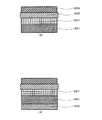
すなわち、図1に示すように、第1基板(図示せず)上に薄膜デバイス層121を形成した後に薄膜デバイス層121上に第1接着層(図示せず)を介して第2基板(図示せず)を接着する。その後、第1基板を分離または除去した後、薄膜デバイス層121の第1基板が形成されていた側を、第2接着層126を介して第3基板127に接着し、第2基板を分離または除去する。このような薄膜デバイスの製造工程において、薄膜デバイス層121が転写される第3基板127の構成体である支持体129として、線膨張係数の低い、例えば線膨張係数が20ppm/K以下であるプラスチック基板(もしくは金属基板)を使用する。そして、複屈折を持つようなプラスチック基板を液晶表示装置に使用する場合には、図示したように、第3基板127に偏光子128と複屈折を持つプラスチックからなる支持体129とを一体化させたものを使用し、偏光子128を薄膜デバイス層121側に貼り付ける。このことによって、複屈折を持つ支持体129は、偏光子128よりも外側にあるため、光が偏光子128を通過した後には影響を与えない。 That is, as shown in FIG. 1, after forming a thin
本発明の薄膜デバイスの製造方法および薄膜デバイスおよび液晶表示装置に係る第1実施例を、図2〜図5の製造工程断面図によって説明する。本実施例では、プラスチック基板を用いた液晶用のアクティブ基板を作製した。 A thin film device manufacturing method, a thin film device and a liquid crystal display device according to a first embodiment of the present invention will be described with reference to manufacturing process cross-sectional views of FIGS. In this example, an active substrate for liquid crystal using a plastic substrate was produced.
まず、薄膜デバイス層の形成方法を図2によって説明する。図2に示すように、第1基板101上に、後に行うフッ酸によるエッチングにおける第1基板101の保護層102を形成する。上記第1基板101には、例えば厚さ0.4mm〜1.1mm程度、例えば0.7mm厚のガラス基板を用いる。このガラス基板のかわりに石英基板を用いてもよい。上記保護層102は、フッ酸に耐えられる材料を用いて形成するもので、例えばモリブデン(Mo)層を用い、例えば500nmの厚さに形成した。今回、モリブデン層の膜厚を500nmとしたが、フッ酸に耐えられるならば、厚さを適宜変更しても問題ない。この保護層102は、例えばスパッタリング法によって成膜することができる。その後、絶縁層103を形成する。この絶縁層103は、例えば酸化珪素(SiO2)膜を500nmの厚さに成膜して形成する。この絶縁層103は、例えばプラズマCVD法によって成膜することができる。First, a method for forming a thin film device layer will be described with reference to FIG. As shown in FIG. 2, a
その後は、一般的な低温ポリシリコン技術、例えば「2003 FPDテクノロジー大全」(電子ジャーナル2003年3月25日発行、p.166−183およびp.198−201)、「'99最新液晶プロセス技術」(プレスジャーナル1998年発行、p.53−59)、「フラットパネル・ディスプレイ1999」(日経BP社、1998年発行、p.132−139)等に記載されているような低温ポリシリコンボトムゲート型薄膜トランジスタ(以下薄膜トランジスタをTFTと記す)プロセスでTFTを含む薄膜デバイス層を形成した。薄膜デバイス層の形成方法の一例を以下に説明する。 Thereafter, general low-temperature polysilicon technology, for example, “2003 FPD Technology Encyclopedia” (published on March 25, 2003, p.166-183 and p.198-201), “'99 latest liquid crystal process technology” (Press Journal 1998, p. 53-59), “Flat Panel Display 1999” (Nikkei Business Publications, 1998, p. 132-139), etc. A thin film device layer including a TFT was formed by a thin film transistor (hereinafter referred to as TFT) process. An example of a method for forming the thin film device layer will be described below.
まず、第1基板101上に保護層102を介して形成された絶縁層103上にゲート電極104を形成するための導電膜を形成した。この導電膜には例えば厚さが100nmのモリブデン(Mo)膜を用いた。モリブデン膜の形成方法としては例えばスパッタリング法を用いた。そして上記導電膜をゲート電極104に形成した。このゲート電極104は、一般的なフォトリソグラフィー技術およびエッチング技術によりパターニングして形成した。次いで、ゲート電極104上を被覆するようにゲート絶縁膜105を形成した。ゲート絶縁膜105は、例えばプラズマCVD法によって、酸化珪素(SiO2)層、または酸化珪素(SiO2)層と窒化珪素(SiNx)層との積層体で形成した。さらに連続的に非晶質シリコン層(厚さ30nm〜100nm)を形成した。First, a conductive film for forming the
この非晶質シリコン層に波長308nmのXeClエキシマレーザパルスを照射し熔融再結晶化し結晶シリコン層(ポリシリコン層)を作製した。このポリシリコン層を用いて、チャネル形成領域となるポリシリコン層106を形成し、その両側にn-型ドープ領域からなるポリシリコン層107、n+型ドープ領域からなるポリシリコン層108を形成した。このように、アクティブ領域は高いオン電流と低いオフ電流を両立するためのLDD(Lightly Doped Drain)構造とした。またポリシリコン層106上にはn-型のリンイオン打込み時にチャネルを保護するためのストッパー層109を形成した。このストッパー層109は、例えば酸化珪素(SiO2)層で形成した。This amorphous silicon layer was irradiated with a XeCl excimer laser pulse having a wavelength of 308 nm and melted and recrystallized to produce a crystalline silicon layer (polysilicon layer). Using this polysilicon layer, a
さらに、プラズマCVD法によって、酸化珪素(SiO2)層、または酸化珪素(SiO2)層と窒化珪素(SiNx)層との積層体からなるパッシベーション膜110を形成した。このパッシベーション膜110上に、各ポリシリコン層108に接続するソース電極111およびドレイン電極112を形成した。各ソース電極111およびドレイン電極112は例えばアルミニウム、アルミニウム合金、高融点金属等の導電性材料で形成した。Further, a
各ソース電極111およびドレイン電極112形成した後、カラーフィルター113を形成した。カラーフィルター113は、カラーレジストを全面に塗布した後、リソグラフィー技術でパターニングを行って形成した。カラーフィルター113には、ソース電極111と後に形成する液晶駆動用電極が接続されるようにコンタクトホール113Cを形成した。このカラーフィルターの形成工程を3回行って、RGBの3色(赤、緑、青)を形成した。次に、平坦化を行うために保護膜114を形成した。保護膜114は例えばポリメチルメタクリル酸樹脂系の樹脂により形成した。また保護膜114には、ソース電極111と液晶駆動用電極とが接続されるようにコンタクトホール114Cを形成した。その後、ソース電極111に接続する画素電極115を形成した。この画素電極115は、例えば、透明電極で形成される。透明電極としては、例えばインジウムスズオキサイド(ITO)により形成され、その形成方法としてはスパッタリング法が用いられる。 After forming each
以上の工程により、第1基板101上に透過型のアクティブマトリックス基板が作製できた。また、今回は、ボトムゲート型ポリシリコンTFTを作製したが、トップゲート型ポリシリコンTFTやアモルファスTFTでも同じように実施できる。 Through the above steps, a transmissive active matrix substrate was fabricated on the
次に、第1基板101上の薄膜デバイス層121をプラスチック基板上に移載する工程を説明する。 Next, a process of transferring the thin
図3(1)に示すように、第1基板101上に保護層102、絶縁層103、薄膜デバイス層121を形成したものをホットプレート122で80℃〜140℃に加熱しながら、第1接着剤123を厚さ1mm程度に塗布し、第2基板124を上に載せ、加圧しながら、室温まで冷却した。第2基板124には、例えば厚さ1mmのモリブデン基板を用いた。または、第2基板124にガラス基板を用いてもよい。または、第2基板124上に第1接着剤123を塗布して、その上に保護層102から薄膜デバイス層121が形成された第1基板101の薄膜デバイス層121側を載せてもよい。上記第1接着剤123には、例えばホットメルト接着剤を用いた。 As shown in FIG. 3 (1), the first bonding is performed while heating the
次に、図3(2)に示すように、第2基板124を貼り付けた第1基板101をフッ酸(HF)125に浸漬して、第1基板101のエッチングを行った。このエッチングは、保護層102である酸化アルミニウム層がフッ酸125にエッチングされないため、このエッチングは保護層102で自動的に停止する。ここで用いたフッ酸125は、一例として、重量濃度が50%のもので、このエッチング時間は3.5時間とした。フッ酸125の濃度とエッチング時間は、第1基板101のガラスを完全にエッチングすることができるならば、変更しても問題はない。 Next, as shown in FIG. 3B, the
上記フッ化水素酸125によるエッチングの結果、図4(3)に示すように、第1基板101〔前記図3(2)参照〕が完全にエッチングされ、保護層102が露出される。 As a result of the etching with
次に、混酸〔例えば、リン酸(H3PO4)72wt%と硝酸(HNO3)3wt%と酢酸(CH3COOH)10wt%〕により、保護層102〔前記図4(3)参照〕であるモリブデン層(厚さ:500nm)をエッチングした。これは、透過型の液晶パネルを作製するために、不透明なモリブデン層があると問題となるためである。上記混酸で500nmの厚さのモリブデン層をエッチングするのに必要な時間は約1分である。このエッチングの結果、図4(4)に示すように、この混酸は第1絶縁層103である酸化珪素をエッチングしないため、第1絶縁層103で自動的にエッチングが停止する。Next, a mixed layer (for example, 72 wt% phosphoric acid (H3 PO4 ),3 wt% nitric acid (HNO3 ), and 10 wt% acetic acid (CH3 COOH)) is used to form the protective layer 102 (see FIG. 4 (3)). A molybdenum layer (thickness: 500 nm) was etched. This is because there is a problem if there is an opaque molybdenum layer in order to manufacture a transmissive liquid crystal panel. The time required to etch a 500 nm thick molybdenum layer with the mixed acid is about 1 minute. As a result of this etching, as shown in FIG. 4 (4), this mixed acid does not etch the silicon oxide that is the first insulating
次に、図4(5)に示すように、上記エッチング後に、薄膜デバイス層121の裏面側、すなわち絶縁層103表面に、第2接着層126を形成した。第2接着層126には例えば紫外線硬化型接着剤を用いた。 Next, as shown in FIG. 4 (5), after the etching, a second
続けて、上記第2接着層126に第3基板127となる偏光板を貼り付けた。上記偏光板は、ヨウ素をPVA(ポリビニアルアルコール)フィルム(例えば、厚さが15μm)に吸収させた後、このフィルムを一軸延伸させ偏光子128とし、偏光子128の片側に支持体129が張り合わされている。この支持体129は、例えば2軸延伸ポリエチレンナフレート(PEN)フィルム128(例えば、厚さが0.2mm)を使用した。このPENフィルムの線膨張係数は13ppm/Kである。このように、第3基板127は、薄膜デバイス層121側に設けられた偏光子128と、薄膜デバイス層121の外側に偏光子128を介して外側に設けられた支持体129とからなる。 Subsequently, a polarizing plate to be the
次に、上記基板をアルコール(図示せず)中に浸漬し、ホットメルト接着剤からなる第1接着層123〔前記図3(1)参照〕を溶かして第2基板124〔前記図3(1)参照〕を外した。その結果、図5(6)に示すように、支持体129と偏光子128とからなる第3基板127上に第2接着層126、絶縁層103を介して薄膜デバイス層121が載った薄膜デバイス(アクティブ基板)100を得た。 Next, the substrate is dipped in alcohol (not shown), and the first adhesive layer 123 (see FIG. 3 (1)) made of a hot-melt adhesive is melted to form the second substrate 124 (see FIG. 3 (1)). ))] Was removed. As a result, as shown in FIG. 5 (6), a thin film device in which a thin
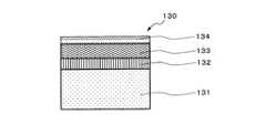
次に、対向基板の製造例を、図6の概略構成断面図によって説明する。 Next, an example of manufacturing the counter substrate will be described with reference to a schematic cross-sectional view of FIG.
図6に示すように、対向基板130として、上記第3基板127(偏光板)と同様なる構造の偏光板を用いた。すなわち、対向基板130は、0.2mm厚の2軸延伸PENフィルムからなる支持体132上に偏光子133を貼り合わせた偏光板を用いるもので、さらに上記偏光子133側の全面に透明電極134を形成したものである。この透明電極134には、例えばITO(インジウムスズオキサイド)を用いた。このITO膜は、例えばスパッタ法により成膜した。 As shown in FIG. 6, a polarizing plate having a structure similar to that of the third substrate 127 (polarizing plate) was used as the
次に、図示はしないが、上記対向基板130とアクティブ基板100とに配向膜(例えばポリイミド膜)を塗布し、ラビング処理を行う配向処理を行った。 Next, although not shown, an alignment film (for example, a polyimide film) is applied to the
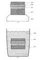
次に、図7に示すように、アクティブ基板100にはシール剤(図示せず)を塗布し、対向基板130には多数のスペーサー135を散布した。 Next, as shown in FIG. 7, a sealant (not shown) was applied to the
そして、アクティブ基板100と対向基板130とを張り合わせた後、例えば1kg/cm2で加圧しながら紫外線を照射してシール剤を硬化させた。次に、レーザー加工によりパネルの大きさに切断した後、注入口から液晶を注入して、注入口をモールド樹脂で覆い、モールド樹脂を硬化させ、液晶表示パネルを作製した。Then, after the
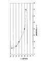
上記工程により作製した液晶表示パネルは、基板となる支持体129、132の線膨張係数が20ppm/K以下と低いため、温度を上げてもクラック等は発生しない。比較のため、異なる線膨張係数のプラスチック基板に転写した薄膜デバイスの耐熱性を図8に示す。図8は、縦軸に耐熱温度を示し、横軸に線膨張係数を示す。また、耐熱温度は、基板を反らないように固定したまま昇温した場合に、クラックの入らない温度の上限を示している。 In the liquid crystal display panel manufactured by the above process, since the linear expansion coefficient of the
図8から分かるように、液晶用基板としては、通常耐熱温度として100℃以上が必要であるため、基板の線膨張係数としては20ppm/Kが必要となることがわかる。また、2軸延伸させたPENフィルムは複屈折を持っているが、偏光子128、133がPENフィルムからなる支持体129、132よりも内部側にあるため、複屈折を漏っていることは問題とならない。なお、上記構造を第3基板127上に直接形成しようとした場合には、偏光子の耐熱温度が低いため、TFTを形成することは難しい。 As can be seen from FIG. 8, the liquid crystal substrate usually needs to have a heat resistant temperature of 100 ° C. or higher, and thus the substrate needs a linear expansion coefficient of 20 ppm / K. Moreover, although the biaxially stretched PEN film has birefringence, since the
上記第1実施例では、第3基板127を構成する支持体129の線膨張係数が20ppm/K以下であるため、薄膜デバイス層121をプラスチック基板である第3基板127に転写した後の耐熱性を高めることができる。また、複屈折を持つプラスチックの第3基板127(実質は支持体129)であっても、偏光子128を薄膜デバイス層121側に設けることによって、液晶表示装置にも使用できるようになる。よって、安価な複屈折を持つ基板を用いることができるようになるため、製造コストの低減が可能となるという利点がある。 In the first embodiment, since the linear expansion coefficient of the
本発明の薄膜デバイスの製造方法および薄膜デバイスおよび液晶表示装置に係る第2実施例を、図9〜図13の製造工程断面図によって説明する。第2実施例では、金属基板上に反射型液晶用のアクティブ基板を作製した。 A manufacturing method of a thin film device and a second embodiment of the thin film device and liquid crystal display device according to the present invention will be described with reference to manufacturing process sectional views of FIGS. In the second example, an active substrate for reflective liquid crystal was produced on a metal substrate.
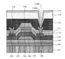
まず、薄膜デバイス層の形成方法を図9によって説明する。図9に示すように、第1基板201上に、第1基板201のアモルファスシリコン層202を形成する。上記第1基板101には、例えば厚さ0.4mm〜1.1mm程度、例えば0.7mm厚のガラス基板を用いる。このガラス基板のかわりに石英基板を用いてもよい。また上記アモルファスシリコン層202の膜厚は、例えば100nmとした。この膜厚は10nm〜500nmが望ましい。アモルファスシリコン層202の成膜方法は、プラズマCVD法を用いた。プラズマCVD法では、アモルファスシリコン層202中に、水素を多く含むように、また製造途中で薄膜デバイス層が剥がれない限りの低温が望ましい。今回は150℃にて成膜を行った。また、低圧CVD法、大気圧CVD法、ECR法、スパッタ法によりアモルファスシリコン層202を成膜しても問題はない。 First, a method for forming a thin film device layer will be described with reference to FIG. As shown in FIG. 9, an
次いで、上記アモルファスシリコン層202上に保護絶縁層203を成膜する。この保護絶縁層203は、例えば100nmの厚さに形成した。この保護絶縁層203は、例えばプラズマCVD法によって成膜することができる。 Next, a protective
その後は、一般的な低温ポリシリコン技術、例えば「2003 FPDテクノロジー大全」(電子ジャーナル2003年3月25日発行、p.166−183およびp.198−201)、「'99最新液晶プロセス技術」(プレスジャーナル1998年発行、p.53−59)、「フラットパネル・ディスプレイ1999」(日経BP社、1998年発行、p.132−139)等に記載されているような低温ポリシリコンボトムゲート型薄膜トランジスタ(以下薄膜トランジスタをTFTと記す)プロセスでTFTを含む薄膜デバイス層を形成した。薄膜デバイス層の形成方法の一例を以下に説明する。 Thereafter, general low-temperature polysilicon technology, for example, “2003 FPD Technology Encyclopedia” (published on March 25, 2003, p.166-183 and p.198-201), “'99 latest liquid crystal process technology” (Press Journal 1998, p. 53-59), “Flat Panel Display 1999” (Nikkei Business Publications, 1998, p. 132-139), etc. A thin film device layer including a TFT was formed by a thin film transistor (hereinafter referred to as TFT) process. An example of a method for forming the thin film device layer will be described below.
まず、第1基板201上にアモルファスシリコン層202を介して形成された保護絶縁層203上にゲート電極204を形成するための導電膜を形成した。この導電膜には例えば厚さが100nmのモリブデン(Mo)膜を用いた。モリブデン膜の形成方法としては例えばスパッタリング法を用いた。そして上記導電膜をゲート電極204に形成した。このゲート電極204は、一般的なフォトリソグラフィー技術およびエッチング技術によりパターニングして形成した。次いで、ゲート電極204上を被覆するようにゲート絶縁膜205を形成した。ゲート絶縁膜205は、例えばプラズマCVD法によって、酸化珪素(SiO2)層、または酸化珪素(SiO2)層と窒化珪素(SiNx)層との積層体で形成した。さらに連続的に非晶質シリコン層(厚さ30nm〜100nm)を形成した。First, a conductive film for forming the
この非晶質シリコン層に波長308nmのXeClエキシマレーザパルスを照射し熔融再結晶化し結晶シリコン層(ポリシリコン層)を作製した。このポリシリコン層を用いて、チャネル形成領域となるポリシリコン層206を形成し、その両側にn-型ドープ領域からなるポリシリコン層207、n+型ドープ領域からなるポリシリコン層208を形成した。このように、アクティブ領域は高いオン電流と低いオフ電流を両立するためのLDD(Lightly Doped Drain)構造とした。またポリシリコン層206上にはn-型のリンイオン打込み時にチャネルを保護するためのストッパー層209を形成した。このストッパー層209は、例えば酸化珪素(SiO2)層で形成した。This amorphous silicon layer was irradiated with a XeCl excimer laser pulse having a wavelength of 308 nm and melted and recrystallized to produce a crystalline silicon layer (polysilicon layer). Using this polysilicon layer, a
さらに、プラズマCVD法によって、酸化珪素(SiO2)層、または酸化珪素(SiO2)層と窒化珪素(SiNx)層との積層体からなるパッシベーション膜210を形成した。このパッシベーション膜210上に、各ポリシリコン層208に接続するソース電極211およびドレイン電極212を形成した。各ソース電極211およびドレイン電極212は例えばアルミニウム、アルミニウム合金、高融点金属等の導電性材料で形成した。Further, a
ソース電極211およびドレイン電極212形成した後、素子を保護するためと平坦化を行うために保護層213を形成した。保護層213は、例えばポリメチルメタクリル樹脂系の材料で形成される。そして、保護層213は、次工程で保護層213上に形成される反射層表面に凹凸が形成されるように、上記保護層213表面が凹凸となるように形成される。次いで、通常のコンタクトホールの形成技術によって、保護膜213に、ソース電極211と後に形成される液晶駆動用電極とが接続されるようにコンタクトホール213Cを形成した。その後、上記保護層213表面およびコンタクトホール213C内面に、反射層214を形成した。この反射層214は、例えばスパッタリングによって銀(Ag)を堆積して形成した。 After forming the
上記反射層214を形成後、カラーフィルター215を形成した。これは、カラーレジストを全面に塗布した後、リソグラフィー技術でパターニングを行って形成した。次いで、カラーフィルター215に、ソース電極211と後に形成される液晶駆動用電極が接続されるようにコンタクトホール215Cを形成した。このカラーフィルターの形成工程を3回行って、RGBの3色(赤、緑、青)を形成した。 After forming the
その後、上記カラーフィルター215表面およびコンタクトホール215C内面に画素電極216を形成した。この画素電極216は、例えばインジウムスズオキサイド(ITO)を、例えばスパッタリングによって堆積して形成した。したがって、画素電極216はソース電極211に接続して形成される。 Thereafter,
以上の工程により、ガラス基板からなる第1基板201上にアクティブマトリックス基板が作製できた。また、今回は、ボトムゲート型ポリシリコンTFTを作製したが、トップゲート型ポリシリコンTFTやアモルファスTFTでも同じように実施できる。 Through the above steps, an active matrix substrate was produced on the
次に、第1基板201上の薄膜デバイス層をプラスチック基板上に移載する工程を説明する。 Next, a process of transferring the thin film device layer on the
図10(1)に示すように、第1基板201上にアモルファスシリコン層202、保護絶縁層203、薄膜デバイス層221を形成したものをホットプレート(図示せず)で80℃〜140℃に加熱しながら、第1接着剤222を塗布し、第2基板223を上に載せ、加圧しながら、室温まで冷却した。第2基板223には、例えば厚さ1mmのモリブデン基板を用いた。または、第2基板223にガラス基板を用いてもよい。または、第2基板223上に第1接着剤222を塗布して、その上にアモルファスシリコン層202から薄膜デバイス層221までが形成された第1基板201の薄膜デバイス層221側を載せてもよい。上記第1接着剤222には、例えばホットメルト接着剤を用いた。 As shown in FIG. 10A, the
次に、ガラス基板からなる第1基板201側から紫外線レーザー光を照射した。ガラスは紫外線レーザーを透過させるため、レーザー光は、アモルファスシリコン層202で吸収される。アモルファスシリコン層202に紫外線が吸収されると水素が発生し、アモルファスシリコン層202を境として薄膜デバイス層221と第1基板201との分離が起きる。この技術の詳細は、特開平10−125930号公報に開示されている。その結果、図10(2)に示すように、保護絶縁層203が露出された。 Next, ultraviolet laser light was irradiated from the
次に、図10(3)に示すように、保護絶縁層203に第2接着層224を形成した。この第2接着層224は、例えばエポキシ系の2液硬化型接着を塗布により形成される。塗布方法は、スプレーコーティング、ディップコーティングもしくはスピンコーティングを用いることができる。 Next, as illustrated in FIG. 10C, the second
続けて図11(4)に示すように、上記第2接着層224に第3基板225を貼り付けた。この第3基板225は、例えば厚さが0.2mmのステンレス基板からなる。ステンレス基板は線膨張係数が16ppm/Kである。本第2実施例の液晶表示装置は、反射型であるため、第3基板225が不透明であってもよい。第3基板225を貼りつけた後、0.5kg/cm2の圧力を加えて保持し、上記第2接着層224を硬化させた。Subsequently, as shown in FIG. 11 (4), the
次に、上記基板をアルコール(図示せず)中に浸漬し、ホットメルト接着剤からなる第1接着層222〔前記図10(1)参照〕を溶かして第2基板223〔前記図10(1)参照〕を外した。その結果、図11(5)に示すように、薄膜デバイス層221が露出され、第3基板225上に第2接着層224、保護絶縁層203を介して薄膜デバイス層221が載った薄膜デバイス(アクティブ基板)200を得た。 Next, the substrate is dipped in alcohol (not shown), and the first adhesive layer 222 (see FIG. 10 (1)) made of hot melt adhesive is melted to form the second substrate 223 (see FIG. 10 (1)). ))] Was removed. As a result, as shown in FIG. 11 (5), the thin
次に、対向基板の製造例を、図12の概略構成断面図によって説明する。 Next, an example of manufacturing the counter substrate will be described with reference to the schematic sectional view of FIG.
図12に示すように、対向基板230として、0.2mm厚の2軸延伸PENフィルムからなる支持体231上に偏光子232とλ/4板233とを張り合わせたものを使用した。さらに上記λ/4板233側の全面に透明電極234を形成したものである。この透明電極234には、例えばITO(インジウムスズオキサイド)を用いた。このITO膜は、例えばスパッタ法により成膜した。 As shown in FIG. 12, a
次に、図示はしないが、上記対向基板230とアクティブ基板200とに配向膜(例えばポリイミド膜)を塗布し、ラビング処理を行う配向処理を行った。 Next, although not shown in the drawing, an alignment film (for example, a polyimide film) is applied to the
次に、図13に示すように、アクティブ基板200にはシール剤(図示せず)を塗布し、対向基板230には多数のスペーサー235を散布した。 Next, as shown in FIG. 13, a sealant (not shown) was applied to the
そして、アクティブ基板200と対向基板230とを張り合わせた後、例えば1kg/cm2で加圧しながら紫外線を照射してシール剤を硬化させた。次にレーザー加工によりパネルの大きさに切断した後、注入口から液晶を注入して、注入口をモールド樹脂で覆い、モールド樹脂を硬化させ、液晶表示パネルを作製した。Then, after the
上記工程により作製した液晶表示パネルは、第3基板225の線膨張係数が20ppm/K以下と低いため、温度を上げてもクラック等は発生しない。 In the liquid crystal display panel manufactured by the above process, since the linear expansion coefficient of the
上記第2実施例では、第3基板225の線膨張係数が20ppm/K以下であるため、薄膜デバイス層221を金属基板である第3基板225に転写した後の耐熱性を高めることができる。よって、安価な金属基板を用いることができるようになるため、製造コストの低減が可能となるという利点がある。 In the said 2nd Example, since the linear expansion coefficient of the 3rd board |
本発明の薄膜デバイスの製造方法および薄膜デバイスおよびエレクトロルミネッセンス表示装置に係る一実施例を、図14〜図17の製造工程断面図によって説明する。この実施例では、転写方式によりプラスチック基板にアクティブマトリックス基板を作製しアクティブマトリックス型有機エレクトロルミネッセンス(以下、エレクトロルミネッセンスをELと略記する)ディスプレイを作製した。 One embodiment of the method for manufacturing a thin film device, the thin film device, and the electroluminescence display device of the present invention will be described with reference to the manufacturing process sectional views of FIGS. In this example, an active matrix substrate was produced on a plastic substrate by a transfer method to produce an active matrix organic electroluminescence (hereinafter abbreviated as EL) display.
図14(1)に示すように、製造基板となる第1基板301に厚さ0.4〜1.1mm程度のガラス基板もしくは石英基板を用いる。そして、例えばスパッタリング法により、第1基板(例えば厚さが0.7mmのガラス基板)301上に薄膜デバイス層を形成する。 As shown in FIG. 14A, a glass substrate or a quartz substrate having a thickness of about 0.4 to 1.1 mm is used for the
すなわち、薄膜デバイス層として、一般的な低温ポリシリコン技術、例えば「2003 FPDテクノロジー大全」(電子ジャーナル2003年3月25日発行、p.166−183およびp.198−201)、「'99最新液晶プロセス技術」(プレスジャーナル1998年発行、p.53−59)、「フラットパネル・ディスプレイ1999」(日経BP社、1998年発行、p.132−139)等に記載されているような低温ポリシリコンボトムゲート型薄膜トランジスタ(以下薄膜トランジスタをTFTと記す)プロセスでTFTを含む薄膜デバイス層を形成した。薄膜デバイス層の形成方法の一例を以下に説明する。 That is, as a thin film device layer, a general low-temperature polysilicon technology, for example, “2003 FPD Technology Encyclopedia” (published on March 25, 2003, p.166-183 and p.198-201), “'99 latest "Liquid crystal process technology" (Press Journal 1998, p. 53-59), "Flat Panel Display 1999" (Nikkei Business Publications, 1998, p. 132-139), etc. A thin film device layer including a TFT was formed by a silicon bottom gate type thin film transistor (hereinafter referred to as a thin film transistor). An example of a method for forming the thin film device layer will be described below.
まず、第1基板301上にゲート電極304を形成するための導電膜を形成した。この導電膜には例えば厚さが100nmのモリブデン(Mo)膜を用いた。モリブデン膜の形成方法としては例えばスパッタリング法を用いた。そして上記導電膜を加工してゲート電極304を形成した。このゲート電極304は、一般的なフォトリソグラフィー技術およびエッチング技術によりパターニングして形成した。次いで、ゲート電極304上を被覆するようにゲート絶縁膜305を形成した。ゲート絶縁膜305は、例えばプラズマCVD法によって、酸化珪素(SiO2)層、または酸化珪素(SiO2)層と窒化珪素(SiNx)層との積層体で形成した。さらに連続的に非晶質シリコン層(厚さ30nm〜100nm)を形成した。First, a conductive film for forming the
この非晶質シリコン層に波長308nmのXeClエキシマレーザパルスを照射し熔融再結晶化し結晶シリコン層を作製した。このポリシリコン層を用いて、チャネル形成領域となるポリシリコン層306を形成し、その両側にn-型ドープ領域からなるポリシリコン層307、n+型ドープ領域からなるポリシリコン層308を形成した。このように、アクティブ領域は高いオン電流と低いオフ電流を両立するためのLDD(Lightly Doped Drain)構造とした。またポリシリコン層306上にはn-型のリンイオン打込み時にチャネルを保護するためのストッパー層309を形成した。このストッパー層309は、例えば酸化シリコン(SiO2)層で形成した。This amorphous silicon layer was irradiated with a XeCl excimer laser pulse having a wavelength of 308 nm, melted and recrystallized to produce a crystalline silicon layer. Using this polysilicon layer, a
さらに、プラズマCVD法によって、酸化珪素(SiO2)層、または酸化珪素(SiO2)層と窒化珪素(SiNx)層との積層体からなるパッシベーション膜310を形成した。このパッシベーション膜310上に、各ポリシリコン層308に接続するソース電極311およびドレイン電極312を形成した。各ソース電極311およびドレイン電極312は例えばアルミニウムで形成した。Further, a
このようにして、低温ポリシリコンボトムゲート型薄膜トランジスタ(TFT)プロセスで薄膜トランジスタ(TFT)を形成した。 In this way, a thin film transistor (TFT) was formed by a low temperature polysilicon bottom gate type thin film transistor (TFT) process.
次に、例えばスピンコート法によって、ソース電極311、ドレイン電極312等を覆うように、パッシベーション膜310上に保護絶縁層313を例えばメタクリル酸メチル樹脂系樹脂で形成した後、一般的なフォトリソグラフィー技術およびエッチング技術により、ソース電極311と後に形成する有機EL素子のアノード電極とを接続できるように、その部分の保護絶縁層313を取り除いた。 Next, after forming a protective
次に、保護絶縁層313上に、有機EL素子を形成した。有機EL素子は、アノード電極314と有機層とカソード電極317とで構成されている。アノード電極314は、例えばスパッタリング法でクロム(Cr)を堆積して形成し、各TFTのソース電極311に接続され、個別に電流を流せるようになっている。 Next, an organic EL element was formed over the protective insulating
有機層は、有機正孔輸送層315と有機発光層316を積層させた構造とした。有機正孔輸送層315としては、例えば銅フタロシアニンを蒸着により30nmの厚さに形成した。有機発光層316は、緑色として、Alq3[tris(8-quinolinolato)aluminium(III)]を50nmの厚さに、青色として、バソクプロイン(Bathocuproine:2,9-dimethyl-4,7-diphenyl-1,10phenanthroline)を14nmの厚さに、赤色としてBSB−BCN[2,5-bis{4-(N-methoxyphenyl-N-phenylamino)styryl}benzene-1,4-dicarbonitrile]を30nmの厚さにそれぞれ蒸着した。 The organic layer has a structure in which an organic
カソード電極317としては、酸化インジウム錫(In2O3+SnO2:ITO)を使用した。As the
今回は、有機EL素子として、上記構造を用いたが、電極に、電子輸送層、正孔輸送層、電子注入層、正孔注入層、電子阻止層、正孔阻止層、発光層を組み合わせた公知の構造を用いてもよい。 This time, the above structure was used as an organic EL element, but an electrode was combined with an electron transport layer, a hole transport layer, an electron injection layer, a hole injection layer, an electron blocking layer, a hole blocking layer, and a light emitting layer. A known structure may be used.
さらに、カソード電極317を覆う形で、パッシベーション膜318を形成した。今回、パッシベーション膜318は、スパッタリング法により窒化シリコン(SiNx)膜を例えば200nmの厚さに形成した。このパッシベーション膜318は、その他、CVD法、蒸着法などで形成してもよい。Further, a
以下、TFT層から有機EL層までを薄膜デバイス層と呼ぶこととする。次に、第1基板301上の薄膜デバイス層をプラスチック基板上に移載する工程を示す。 Hereinafter, the TFT layer to the organic EL layer are referred to as a thin film device layer. Next, a process of transferring the thin film device layer on the
図15(1)に示すように第1基板301上に薄膜デバイス層321を形成したものをホットプレート322で80℃〜140℃に加熱しながら、第1接着層323を、例えばホットメルト接着剤を例えば1mm程度の厚さに塗布して形成した。次に、上記第1接着層323上に第2基板324を載せ、第2基板324を第1基板301方向に加圧しながら、室温まで冷却した。上記第2基板324には、例えば厚さが1mmのモリブデン(Mo)基板を用いた。または、第2基板324上にホットメルト接着剤を塗布して、その上に薄膜デバイス層321が形成された第1基板301の薄膜デバイス層321側を載せてもよい。 As shown in FIG. 15 (1), the first
次に、図15(2)に示すように、第2基板324を貼り付けた基板をフッ化水素酸325に浸漬して、第1基板301のエッチングを行った。このエッチングでは、第1基板301を、例えばおよそ30μmの厚さになるように残すように行うため、エッチング終点は例えばエッチング時間により制御する。一例として、ここで用いたフッ化水素酸325は重量濃度15%〜25%のもので、このエッチング時間はエアーブローによるバブリングによって弗化水素酸溶液を攪拌しながら室温で約3時間とした。フッ化水素酸325の濃度とエッチング時間は、適宜変更しても問題はない。上記エッチングの代わりに、例えば機械的な研磨、化学的機械研磨等の研磨によって、第1基板301を薄くしても良い。 Next, as illustrated in FIG. 15B, the
上記フッ化水素酸325によるエッチングの結果、図16(3)に示すように、第1基板301上に薄膜デバイス層321が形成され、さらに薄膜デバイス層321上に第1接着層323を介して第2基板324が形成されたものが得られる。 As a result of the etching with
その後、図16(4)に示すように、上記第1基板301の上記薄膜デバイス層321が形成されている面とは反対側の面に第2接着層326を形成する。上記第2接着層326は、一例として、回転塗布技術により例えばアクリル系の紫外線硬化接着剤を塗布して形成した。回転塗布技術による膜形成では、膜厚を約10μmとした。 Thereafter, as shown in FIG. 16D, a second
続けて、図17(5)に示すように、上記第2接着層326に第3基板(プラスチック基板)327を貼り付けた。第3基板(プラスチック基板)327にはポリエチレンテレフタラート(PET)フィルムを用い、このPETフィルムには例えば0.2mmの厚さのものを用いた。このPETフィルムの線膨張係数は16ppm/Kである。 Subsequently, as shown in FIG. 17 (5), a third substrate (plastic substrate) 327 was attached to the second
次に、上記基板をアルコール(図示せず)中に浸漬し、ホットメルト接着剤からなる第1接着層322〔前記図15(1)参照〕を溶かして第2基板323〔前記図15(1)参照〕を外し、図17(6)に示すように、第3基板327上に第2接着層326、第1基板301を介して薄膜デバイス層321が載った薄膜デバイス(アクティブ基板)300を得た。 Next, the substrate is immersed in alcohol (not shown), and the first adhesive layer 322 (see FIG. 15 (1)) made of a hot-melt adhesive is melted to form the second substrate 323 [see FIG. 15 (1). 17), and a thin film device (active substrate) 300 in which the thin
その後の工程は、一般的に行われている有機ELの組立工程を行えばよい。
上記工程により作製した薄膜デバイスは、TFT基板の線膨張係数が低いため、温度を上げてもクラック等は発生しない。Subsequent steps may be assembling the organic EL that is generally performed.
Since the thin film device manufactured by the above process has a low coefficient of linear expansion of the TFT substrate, cracks and the like do not occur even when the temperature is increased.
この後は、図示はしないが、一般的に行われている有機エレクトロルミネッセンス表示装置の組立工程で行えばよい。 Thereafter, although not shown in the drawing, it may be carried out in a generally assembled process of an organic electroluminescence display device.
上記実施例では、第3基板327の線膨張係数が20ppm/K以下であるため、転写後の耐熱性を上げることができる。よって、安価なプラスチック基板を用いることができるようになるため、製造コストの低減が可能となるという利点がある。 In the above embodiment, since the
本発明の薄膜デバイスの製造方法、薄膜デバイス、液晶表示装置およびエレクトロルミネッセンス表示装置は、各種表示装置の用途に適用できる。 The thin film device manufacturing method, thin film device, liquid crystal display device and electroluminescence display device of the present invention can be applied to various display devices.
121…薄膜デバイス層、123…第1接着層、124…第2基板、126…第2接着層、127…第3基板 121 ... Thin film device layer, 123 ... First adhesive layer, 124 ... Second substrate, 126 ... Second adhesive layer, 127 ... Third substrate
Claims (4)
Translated fromJapanese化学処理および機械的研磨処理および紫外線照射処理の少なくとも一つの処理を含む工程により前記第1基板を完全または部分的に分離または除去する工程と、
前記薄膜デバイス層の第1基板が形成されていた側または部分的に残した第1基板に、第2接着層を介して、偏光板としての第3基板を接着する工程と、
前記第2基板を分離または除去する工程と
を備えた薄膜デバイスの製造方法において、
前記第3基板として、前記薄膜デバイス層側から順に、偏光子と、線膨張係数が20ppm/K以下であると共に複屈折を有する支持体とを有するものを用いる
薄膜デバイスの製造方法。Forminga thin film device layerincluding a transistor on the first substrate and then bonding the second substrate on the thin film device layer via the first adhesive layer or the covering layer and the first adhesive layer;
Separating or removing the first substrate completely or partially by a process including at least one of chemical treatment, mechanical polishing treatment, and ultraviolet irradiation treatment;
The first substrate leaving a the thin film device layer first side or partial substrate were formed of a step via a second adhesivelayer, bondingthe thirdsubstrate as a polarizing plate,
A method of manufacturing a thin film device comprising: separating or removing the second substrate;
The manufacturing method of the thin film deviceusing what has a polarizer and a support body which has a linear expansion coefficient below 20 ppm / K and has birefringence in order from the said thin film device layer side as said 3rd board| substrate .
前記支持体は2軸延伸して形成されたプラスチックフィルムよりなる The support is made of a plastic film formed by biaxial stretching.
請求項1に記載の薄膜デバイスの製造方法。 The method for manufacturing a thin film device according to claim 1.
化学処理および機械的研磨処理および紫外線照射処理の少なくとも一つの処理を含む工程により前記第1基板を完全または部分的に分離または除去する工程と、
前記薄膜デバイス層の第1基板が形成されていた側または部分的に残した第1基板に、第2接着層を介して、偏光板としての第3基板を接着する工程と、
前記第2基板を分離または除去する工程と
により製造される薄膜デバイスにおいて、
前記第3基板が、前記薄膜デバイス層側から順に、偏光子と、線膨張係数が20ppm/K以下であると共に複屈折を有する支持体とを有する
薄膜デバイス。Forminga thin film device layerincluding a transistor on the first substrate and then bonding the second substrate on the thin film device layer via the first adhesive layer or the covering layer and the first adhesive layer;
Separating or removing the first substrate completely or partially by a process including at least one of chemical treatment, mechanical polishing treatment, and ultraviolet irradiation treatment;
The first substrate leaving a the thin film device layer first side or partial substrate were formed of a step via a second adhesivelayer, bondingthe thirdsubstrate as a polarizing plate,
In the thin film device manufactured by separating or removing the second substrate,
Thethin film device in which the third substrateincludes, in order from the thin film device layer side, a polarizer and a support having a linear expansion coefficient of 20 ppm / K or less and birefringence .
化学処理および機械的研磨処理および紫外線照射処理の少なくとも一つの処理を含む工程により前記第1基板を完全または部分的に分離または除去する工程と、
前記薄膜デバイス層の第1基板が形成されていた側または部分的に残した第1基板に、第2接着層を介して、偏光板としての第3基板を接着する工程と、
前記第2基板を分離または除去する工程と
により製造される薄膜デバイスを用いた液晶表示装置において、
前記第3基板が、前記薄膜デバイス層側から順に、偏光子と、線膨張係数が20ppm/K以下であると共に複屈折を有する支持体とを有する
液晶表示装置。Forminga thin film device layerincluding a transistor on the first substrate and then bonding the second substrate on the thin film device layer via the first adhesive layer or the covering layer and the first adhesive layer;
Separating or removing the first substrate completely or partially by a process including at least one of chemical treatment, mechanical polishing treatment, and ultraviolet irradiation treatment;
The first substrate leaving a the thin film device layer first side or partial substrate were formed of a step via a second adhesivelayer, bondingthe thirdsubstrate as a polarizing plate,
In a liquid crystal display device using a thin film device manufactured by separating or removing the second substrate,
The liquid crystal display device inwhich the third substrateincludes, in order from the thin film device layer side, a polarizer and a support having a linear expansion coefficient of 20 ppm / K or less and birefringence .
Priority Applications (1)
| Application Number | Priority Date | Filing Date | Title |
|---|---|---|---|
| JP2003417458AJP4759917B2 (en) | 2003-12-16 | 2003-12-16 | Thin film device manufacturing method, thin film device, and liquid crystal display device |
Applications Claiming Priority (1)
| Application Number | Priority Date | Filing Date | Title |
|---|---|---|---|
| JP2003417458AJP4759917B2 (en) | 2003-12-16 | 2003-12-16 | Thin film device manufacturing method, thin film device, and liquid crystal display device |
Publications (2)
| Publication Number | Publication Date |
|---|---|
| JP2005183414A JP2005183414A (en) | 2005-07-07 |
| JP4759917B2true JP4759917B2 (en) | 2011-08-31 |
Family
ID=34779948
Family Applications (1)
| Application Number | Title | Priority Date | Filing Date |
|---|---|---|---|
| JP2003417458AExpired - Fee RelatedJP4759917B2 (en) | 2003-12-16 | 2003-12-16 | Thin film device manufacturing method, thin film device, and liquid crystal display device |
Country Status (1)
| Country | Link |
|---|---|
| JP (1) | JP4759917B2 (en) |
Families Citing this family (5)
| Publication number | Priority date | Publication date | Assignee | Title |
|---|---|---|---|---|
| KR100615222B1 (en)* | 2004-06-17 | 2006-08-25 | 삼성에스디아이 주식회사 | Electroluminescent display device and manufacturing method thereof |
| KR100824880B1 (en) | 2006-11-10 | 2008-04-23 | 삼성에스디아이 주식회사 | Organic electroluminescent display and manufacturing method thereof |
| KR100824881B1 (en) | 2006-11-10 | 2008-04-23 | 삼성에스디아이 주식회사 | Organic electroluminescent display and manufacturing method thereof |
| KR100824902B1 (en) | 2006-12-13 | 2008-04-23 | 삼성에스디아이 주식회사 | Organic electroluminescent display and manufacturing method thereof |
| JP5334236B2 (en)* | 2007-07-25 | 2013-11-06 | 株式会社プライマテック | Field effect transistor |
Family Cites Families (3)
| Publication number | Priority date | Publication date | Assignee | Title |
|---|---|---|---|---|
| US5376561A (en)* | 1990-12-31 | 1994-12-27 | Kopin Corporation | High density electronic circuit modules |
| JP3915381B2 (en)* | 2000-07-31 | 2007-05-16 | セイコーエプソン株式会社 | Liquid crystal device and electronic device |
| TW574753B (en)* | 2001-04-13 | 2004-02-01 | Sony Corp | Manufacturing method of thin film apparatus and semiconductor device |
- 2003
- 2003-12-16JPJP2003417458Apatent/JP4759917B2/ennot_activeExpired - Fee Related
Also Published As
| Publication number | Publication date |
|---|---|
| JP2005183414A (en) | 2005-07-07 |
Similar Documents
| Publication | Publication Date | Title |
|---|---|---|
| US8168511B2 (en) | Display device manufacturing method and laminated structure | |
| US7466390B2 (en) | Active matrix displays and other electronic devices having plastic substrates | |
| JP4052631B2 (en) | Active matrix display device | |
| TWI362547B (en) | Peeling method and method for manufacturing display device using the peeling method | |
| JPWO2002084739A1 (en) | Method of manufacturing thin film device and semiconductor device | |
| TW200300281A (en) | Semiconductor device and method of manufacturing the same | |
| CN101176029A (en) | Color Active Matrix Display | |
| JP2010224426A (en) | Display device | |
| JP2012027177A (en) | Method of manufacturing flexible thin film transistor substrate | |
| JP2003323132A (en) | Method for manufacturing thin film device and semiconductor device | |
| JP4063225B2 (en) | Liquid crystal display device and method of manufacturing liquid crystal display device | |
| JP2005017567A (en) | Liquid crystal display device and its manufacturing method, and electro luminescence display device and its manufacturing method | |
| JP4759917B2 (en) | Thin film device manufacturing method, thin film device, and liquid crystal display device | |
| JP2005209756A (en) | Thin film device, manufacturing method therefor crystal display device, and electroluminescence display device | |
| US20040147092A1 (en) | Method for fabricating thin film transistor display device | |
| JP2005085830A (en) | Thin film device and method for manufacturing the same | |
| JP2004259796A (en) | Method of manufacturing thin film device and thin film device | |
| JP4716081B2 (en) | Manufacturing method of liquid crystal display device | |
| JP2005019054A (en) | Thin film device, manufacturing method for thin film device, liquid crystal display and electroluminescence display | |
| JP4621713B2 (en) | Active matrix display device | |
| JP2005216887A (en) | Method of manufacturing thin film device, thin film device, liquid crystal display device and electroluminescence display device | |
| JP3926116B2 (en) | Manufacturing method of semiconductor device, manufacturing method of liquid crystal display device, and manufacturing method of EL display device | |
| JP2005308849A (en) | Thin film device, manufacturing method for same, liquid crystal display apparatus and electroluminescence display device | |
| JP3850324B2 (en) | Active matrix display device and manufacturing method thereof | |
| JP2004327872A (en) | Thin film transistor, its manufacturing method, display device using the thin film transistor and its manufacturing method |
Legal Events
| Date | Code | Title | Description |
|---|---|---|---|
| A621 | Written request for application examination | Free format text:JAPANESE INTERMEDIATE CODE: A621 Effective date:20060706 | |
| RD02 | Notification of acceptance of power of attorney | Free format text:JAPANESE INTERMEDIATE CODE: A7422 Effective date:20091021 | |
| A521 | Request for written amendment filed | Free format text:JAPANESE INTERMEDIATE CODE: A821 Effective date:20091026 | |
| RD04 | Notification of resignation of power of attorney | Free format text:JAPANESE INTERMEDIATE CODE: A7424 Effective date:20091104 | |
| A977 | Report on retrieval | Free format text:JAPANESE INTERMEDIATE CODE: A971007 Effective date:20100727 | |
| A131 | Notification of reasons for refusal | Free format text:JAPANESE INTERMEDIATE CODE: A131 Effective date:20100803 | |
| A521 | Request for written amendment filed | Free format text:JAPANESE INTERMEDIATE CODE: A523 Effective date:20100927 | |
| TRDD | Decision of grant or rejection written | ||
| A01 | Written decision to grant a patent or to grant a registration (utility model) | Free format text:JAPANESE INTERMEDIATE CODE: A01 Effective date:20110510 | |
| A61 | First payment of annual fees (during grant procedure) | Free format text:JAPANESE INTERMEDIATE CODE: A61 Effective date:20110523 | |
| FPAY | Renewal fee payment (event date is renewal date of database) | Free format text:PAYMENT UNTIL: 20140617 Year of fee payment:3 | |
| R151 | Written notification of patent or utility model registration | Ref document number:4759917 Country of ref document:JP Free format text:JAPANESE INTERMEDIATE CODE: R151 | |
| FPAY | Renewal fee payment (event date is renewal date of database) | Free format text:PAYMENT UNTIL: 20140617 Year of fee payment:3 | |
| FPAY | Renewal fee payment (event date is renewal date of database) | Free format text:PAYMENT UNTIL: 20140617 Year of fee payment:3 | |
| S111 | Request for change of ownership or part of ownership | Free format text:JAPANESE INTERMEDIATE CODE: R313113 | |
| FPAY | Renewal fee payment (event date is renewal date of database) | Free format text:PAYMENT UNTIL: 20140617 Year of fee payment:3 | |
| R350 | Written notification of registration of transfer | Free format text:JAPANESE INTERMEDIATE CODE: R350 | |
| R250 | Receipt of annual fees | Free format text:JAPANESE INTERMEDIATE CODE: R250 | |
| R250 | Receipt of annual fees | Free format text:JAPANESE INTERMEDIATE CODE: R250 | |
| R250 | Receipt of annual fees | Free format text:JAPANESE INTERMEDIATE CODE: R250 | |
| R250 | Receipt of annual fees | Free format text:JAPANESE INTERMEDIATE CODE: R250 | |
| R250 | Receipt of annual fees | Free format text:JAPANESE INTERMEDIATE CODE: R250 | |
| R250 | Receipt of annual fees | Free format text:JAPANESE INTERMEDIATE CODE: R250 | |
| R250 | Receipt of annual fees | Free format text:JAPANESE INTERMEDIATE CODE: R250 | |
| S111 | Request for change of ownership or part of ownership | Free format text:JAPANESE INTERMEDIATE CODE: R313111 | |
| R250 | Receipt of annual fees | Free format text:JAPANESE INTERMEDIATE CODE: R250 | |
| R350 | Written notification of registration of transfer | Free format text:JAPANESE INTERMEDIATE CODE: R350 | |
| R250 | Receipt of annual fees | Free format text:JAPANESE INTERMEDIATE CODE: R250 | |
| LAPS | Cancellation because of no payment of annual fees |