JP4757607B2 - Semiconductor memory - Google Patents
Semiconductor memoryDownload PDFInfo
- Publication number
- JP4757607B2 JP4757607B2JP2005324028AJP2005324028AJP4757607B2JP 4757607 B2JP4757607 B2JP 4757607B2JP 2005324028 AJP2005324028 AJP 2005324028AJP 2005324028 AJP2005324028 AJP 2005324028AJP 4757607 B2JP4757607 B2JP 4757607B2
- Authority
- JP
- Japan
- Prior art keywords
- cell array
- control unit
- semiconductor memory
- read
- signal control
- Prior art date
- Legal status (The legal status is an assumption and is not a legal conclusion. Google has not performed a legal analysis and makes no representation as to the accuracy of the status listed.)
- Expired - Fee Related
Links
Images


Classifications
- G—PHYSICS
- G11—INFORMATION STORAGE
- G11C—STATIC STORES
- G11C11/00—Digital stores characterised by the use of particular electric or magnetic storage elements; Storage elements therefor
- G11C11/21—Digital stores characterised by the use of particular electric or magnetic storage elements; Storage elements therefor using electric elements
- G11C11/34—Digital stores characterised by the use of particular electric or magnetic storage elements; Storage elements therefor using electric elements using semiconductor devices
- G11C11/40—Digital stores characterised by the use of particular electric or magnetic storage elements; Storage elements therefor using electric elements using semiconductor devices using transistors
- G11C11/41—Digital stores characterised by the use of particular electric or magnetic storage elements; Storage elements therefor using electric elements using semiconductor devices using transistors forming static cells with positive feedback, i.e. cells not needing refreshing or charge regeneration, e.g. bistable multivibrator or Schmitt trigger
- G11C11/413—Auxiliary circuits, e.g. for addressing, decoding, driving, writing, sensing, timing or power reduction
- G—PHYSICS
- G11—INFORMATION STORAGE
- G11C—STATIC STORES
- G11C7/00—Arrangements for writing information into, or reading information out from, a digital store
- G11C7/18—Bit line organisation; Bit line lay-out
Landscapes
- Engineering & Computer Science (AREA)
- Microelectronics & Electronic Packaging (AREA)
- Computer Hardware Design (AREA)
- Static Random-Access Memory (AREA)
- Semiconductor Memories (AREA)
- For Increasing The Reliability Of Semiconductor Memories (AREA)
Description
Translated fromJapanese本発明は、複数のセルアレイと、これ等セルアレイに共通のグローバルビット線とを有する半導体メモリに関する。 The present invention relates to a semiconductor memory having a plurality of cell arrays and global bit lines common to these cell arrays.
一般に、SRAM等の半導体メモリでは、メモリセルに接続されるビット線は、メモリ容量の増加とともに長くなる傾向がある。ビット線が長くなると、ビット線の負荷容量は増加し、アクセス時間は長くなる。アクセス時間がビット線の負荷容量により長くなることを防止するために、階層構造を有するビット線が提案されている(例えば、特許文献1参照)。この手法では、互いに独立のビット線を有する複数のセルアレイが形成され、これ等セルアレイに共通のグローバルビット線が配線される。
一方、1チップにロジック回路とメモリ回路(半導体メモリ)が搭載されるシステムLSIには、ユーザ仕様に応じてメモリ容量を設定できるものがある。この種のシステムLSIでは、半導体メモリは、システムLSIの設計ツールの一つであるコンパイラを使用してRAMマクロとして形成される。例えば、コンパイラは、メモリ容量に応じてワード線の本数を計算し、各ワード線にアドレスを割り当てる。 On the other hand, some system LSIs in which a logic circuit and a memory circuit (semiconductor memory) are mounted on one chip can set a memory capacity according to user specifications. In this type of system LSI, the semiconductor memory is formed as a RAM macro using a compiler that is one of the design tools for the system LSI. For example, the compiler calculates the number of word lines according to the memory capacity, and assigns an address to each word line.
コンパイラは、所定のメモリ容量を有する基本セルアレイ(完全セルアレイ)をライブラリとして有している。コンパイラは、チップ上に形成する基本セルアレイの数を、ユーザが希望するメモリ容量に応じて計算する。メモリ容量が、基本セルアレイの容量の整数倍でない場合、コンパイラは、基本セルアレイより小さい不完全セルアレイを形成する。一般的なレイアウト設計では、基本セルアレイは、I/O回路に近い側に配置され、不完全セルアレイは、I/O回路に最も遠い側に配置される。各セルアレイのビット線およびセルアレイに共通のグローバルビット線は、セルアレイの配列方向に沿って配線される。 The compiler has a basic cell array (complete cell array) having a predetermined memory capacity as a library. The compiler calculates the number of basic cell arrays formed on the chip according to the memory capacity desired by the user. If the memory capacity is not an integer multiple of the basic cell array capacity, the compiler forms an incomplete cell array smaller than the basic cell array. In a general layout design, the basic cell array is arranged on the side closest to the I / O circuit, and the incomplete cell array is arranged on the side farthest from the I / O circuit. The bit line of each cell array and the global bit line common to the cell array are wired along the array direction of the cell array.
グローバルビット線の負荷容量は、グローバルビット線が長いほど大きくなる。そのため、グローバルビット線が長く、グローバルビット線の負荷容量が大きいと、半導体メモリのアクセス時にグローバルビット線の充放電電流が大きくなる。この結果、消費電力が増加し、アクセス時間が増加する。しかしながら、従来、セルアレイを配置するときに、グローバルビット線の長さは考慮されていない。 The load capacity of the global bit line increases as the global bit line becomes longer. Therefore, if the global bit line is long and the load capacity of the global bit line is large, the charge / discharge current of the global bit line increases when the semiconductor memory is accessed. As a result, power consumption increases and access time increases. However, conventionally, the length of the global bit line is not taken into consideration when arranging the cell array.
本発明の目的は、セルアレイの配置を工夫することで、グローバルビット線の長さを短縮し、半導体メモリの消費電力を減少することにある。また、半導体メモリのアクセス時間を短縮することにある。 An object of the present invention is to devise the arrangement of the cell array to shorten the length of the global bit line and reduce the power consumption of the semiconductor memory. Another object is to shorten the access time of the semiconductor memory.
本発明の一形態では、メモリセル、ビット線およびワード線を有するセルアレイは、一方向に配列されている。セルアレイは、所定のメモリ容量を有する少なくとも一つの完全セルアレイと、所定のメモリ容量に満たない容量を有する不完全セルアレイのいずれかである。不完全セルアレイは、完全セルアレイより信号制御部の近くに配置されており、配列方向の長さが完全セルアレイより短い。信号制御部は、セルアレイの列の一端側に配置され、グローバル線に信号を入力または出力する。読み書き制御部は、セルアレイの間に配置され、セルアレイに対するデータの読み書きを制御する。グローバル線は、セルアレ
イの列の一端からセルアレイの配列方向に向けて配線され、読み書き制御部に接続されている。信号制御部と読み書き制御部との間に信号を伝達するグローバル線は、長さの短い不完全セルアレイ上に必ず配線される。このため、グローバル線を完全セルアレイ上に配線する場合に比べてその配線長を短くできる。したがって、グローバル線の負荷容量を削減でき、セルアレイの動作時に発生するグローバル線の充放電電流を削減できる。この結果、半導体メモリの消費電力を削減でき、半導体メモリのアクセス時間を短縮できる。In one embodiment of the present invention, a cell array having memory cells, bit lines, and word lines is arranged in one direction. The cell array is either at least one complete cell array having a predetermined memory capacity or an incomplete cell array having a capacity less than the predetermined memory capacity. The incomplete cell array is arranged closer to the signal control unit than the complete cell array, and the length in the arrangement direction is shorter than the complete cell array. The signal control unit is disposed on one end side of the column of the cell array, and inputs or outputs a signal to the global line. The read / write control unit is disposed between the cell arrays and controls reading / writing of data with respect to the cell array. The global line is wired from one end of the cell array column toward the array direction of the cell array, and is connected to the read / write control unit. A global line for transmitting a signal between the signal control unit and the read / write control unit is always wired on an incomplete cell array having a short length. For this reason, the wiring length can be shortened compared with the case where the global line is wired on the complete cell array. Therefore, the load capacity of the global line can be reduced, and the charge / discharge current of the global line generated during the operation of the cell array can be reduced. As a result, the power consumption of the semiconductor memory can be reduced, and the access time of the semiconductor memory can be shortened.
本発明の一形態における好ましい例では、信号制御部は、セルアレイにデータを入出力するデータ入出力部である。グローバル線は、セルアレイとデータ入出力部の間にデータを伝達するグローバルビット線である。一般に、半導体メモリでは、データの転送レートを向上するために、複数のグローバルビット線が形成される場合が多い。本発明の適用により、複数のグローバルビット線の充放電電流が削減できるため、消費電力の削減効果は大きい。 In a preferred example of one aspect of the present invention, the signal control unit is a data input / output unit that inputs / outputs data to / from the cell array. The global line is a global bit line that transmits data between the cell array and the data input / output unit. In general, in a semiconductor memory, a plurality of global bit lines are often formed in order to improve a data transfer rate. By applying the present invention, charge / discharge currents of a plurality of global bit lines can be reduced, so that the effect of reducing power consumption is great.
本発明の一形態における好ましい例では、ワード線を選択するために割り当てられたアドレスは、信号制御部に遠い側から近い側に向けて昇順である。不完全セルアレイは、最大のアドレスが割り当てられたワード線を含む。アドレスを順序正しく割り当てることで、アドレスデコーダ等の回路設計を容易にできる。また、半導体メモリに不良が発生したときに、不良アドレスを物理的に特定しやすいため、不良解析の効率を向上できる。 In a preferred example of one aspect of the present invention, the addresses assigned to select word lines are in ascending order from the far side to the near side to the signal control unit. The incomplete cell array includes a word line to which the maximum address is assigned. By assigning addresses in order, circuit design such as an address decoder can be facilitated. In addition, when a defect occurs in the semiconductor memory, it is easy to physically specify a defective address, so that the efficiency of defect analysis can be improved.
本発明の一形態における好ましい例では、各メモリユニットは、一対のセルアレイと読み書き制御部により構成される。読み書き制御部は、一対のセルアレイの間に配置され、これ等セルアレイに共有される。不完全セルアレイは、メモリユニットのいずれかに含まれ、対応する読み書き制御部の信号制御部側に配置されている。これにより、グローバル線は、常に不完全セルアレイ上に配線される。したがって、複数の完全セルアレイと1つの不完全セルアレイとが形成される場合にも、グローバル線の充放電電流を削減できる。 In a preferred example of one embodiment of the present invention, each memory unit includes a pair of cell arrays and a read / write controller. The read / write control unit is arranged between a pair of cell arrays and is shared by these cell arrays. The incomplete cell array is included in one of the memory units and is arranged on the signal control unit side of the corresponding read / write control unit. As a result, the global line is always wired on the incomplete cell array. Therefore, even when a plurality of complete cell arrays and one incomplete cell array are formed, the charge / discharge current of the global line can be reduced.
本発明の一形態における好ましい例では、不完全セルアレイを含むメモリユニットは、信号制御部に最も近い位置に配置されている。セルアレイにおいて、ワード線を選択するために割り当てられたアドレスは、信号制御部に遠い側から近い側に向けて昇順である。不完全セルアレイは、最大のアドレスが割り当てられたワード線を含む。複数の完全セルアレイと1つの不完全セルアレイとが形成される場合にも、アドレスを順序正しく割り当てることで、アドレスデコーダ等の回路設計を容易にできる。また、半導体メモリに不良が発生したときに、不良アドレスを物理的に特定しやすいため、不良解析の効率を向上できる。 In a preferred example of one embodiment of the present invention, the memory unit including the incomplete cell array is disposed at a position closest to the signal control unit. In the cell array, the addresses assigned to select the word lines are in ascending order from the far side to the near side to the signal control unit. The incomplete cell array includes a word line to which the maximum address is assigned. Even when a plurality of complete cell arrays and one incomplete cell array are formed, circuit design such as an address decoder can be facilitated by assigning addresses in order. In addition, when a defect occurs in the semiconductor memory, it is easy to physically specify a defective address, so that the efficiency of defect analysis can be improved.
本発明の一形態における好ましい例では、グローバル線は、複数のサブグローバル線により構成される。リピータ回路は、各メモリユニットの読み書き制御部の形成領域に形成されている。リピータ回路は、信号制御部に遠いサブグローバル線を、信号制御部に近いサブグローバル線に接続する。不完全セルアレイを含むメモリユニットは、信号制御部に最も遠い位置に配置されている。リピータ回路の挿入により、不完全セルアレイを含むメモリユニットがアクセスされるとき、このメモリユニットに接続されたサブグローバル線は、信号制御部に接続され充放電される。一方、不完全セルアレイを含まないメモリユニットがアクセスされるとき、不完全セルアレイを含むメモリユニットに接続されたサブグローバル線は、信号制御部から切り離され充放電されない。したがって、不完全セルアレイを含まないメモリユニットをアクセスするときの消費電力は、不完全セルアレイを含むメモリユニットをアクセスするときの消費電力より低くなる。 In a preferred example of one aspect of the present invention, the global line is constituted by a plurality of sub-global lines. The repeater circuit is formed in the formation area of the read / write controller of each memory unit. The repeater circuit connects a subglobal line far from the signal control unit to a subglobal line close to the signal control unit. The memory unit including the incomplete cell array is arranged at a position farthest from the signal control unit. When a memory unit including an incomplete cell array is accessed by inserting a repeater circuit, a subglobal line connected to the memory unit is connected to a signal control unit and charged / discharged. On the other hand, when a memory unit that does not include an incomplete cell array is accessed, the subglobal lines connected to the memory unit that includes the incomplete cell array are disconnected from the signal control unit and are not charged / discharged. Therefore, the power consumption when accessing a memory unit that does not include an incomplete cell array is lower than the power consumption when accessing a memory unit that includes an incomplete cell array.
半導体メモリがランダムアクセスされるとき、完全セルアレイを含むメモリユニットのアクセス頻度は、小さいメモリ容量を有する不完全セルアレイを含むメモリユニットのア
クセス頻度より高くなる。リピータ回路が挿入される場合に、セルアレイの配置を工夫し、アクセス頻度の高いメモリユニットの消費電力を下げることで、半導体メモリの消費電力を削減でき、半導体メモリのアクセス時間を短縮できる。When the semiconductor memory is randomly accessed, the access frequency of the memory unit including the complete cell array is higher than the access frequency of the memory unit including the incomplete cell array having a small memory capacity. When a repeater circuit is inserted, the arrangement of the cell array is devised, and the power consumption of the memory unit with high access frequency is reduced, so that the power consumption of the semiconductor memory can be reduced and the access time of the semiconductor memory can be shortened.
本発明の一形態における好ましい例では、不完全セルアレイを含まないメモリユニットにおいて、ワード線を選択するために割り当てられたアドレスは、信号制御部に近い側から遠い側に向けて昇順である。不完全セルアレイを含むメモリユニットにおいて、ワード線を選択するために割り当てられたアドレスは、信号制御部に遠い側から近い側に向けて昇順である。不完全セルアレイは、最大のアドレスが割り当てられたワード線を含む。一般に、不完全セルアレイと完全セルアレイを有する半導体メモリの設計では、不完全セルアレイは、完全セルアレイを配置した後に配置することが多い。このため、不完全セルアレイのアドレスを、完全セルアレイのアドレスより大きくすることで、アドレスを順次割り当てながらセルアレイを設計できる。この結果、設計効率を向上できる。特に、不完全セルアレイを有する半導体メモリは、コンパイラ等の設計ツールを用いて自動で設計する場合が多い。この場合に、設計ツールのプログラムを簡易に設計できる。 In a preferred example of one embodiment of the present invention, in a memory unit that does not include an incomplete cell array, addresses assigned to select a word line are in ascending order from a side closer to the signal control unit to a side farther from the signal control unit. In a memory unit including an incomplete cell array, addresses assigned to select a word line are in ascending order from the side far from the signal control unit toward the side closer to the signal control unit. The incomplete cell array includes a word line to which the maximum address is assigned. In general, in designing a semiconductor memory having an incomplete cell array and a complete cell array, the incomplete cell array is often arranged after the complete cell array is arranged. Therefore, by making the address of the incomplete cell array larger than the address of the complete cell array, the cell array can be designed while sequentially assigning addresses. As a result, design efficiency can be improved. In particular, a semiconductor memory having an incomplete cell array is often designed automatically using a design tool such as a compiler. In this case, the design tool program can be designed easily.
本発明の一形態における好ましい例では、半導体メモリは、回路情報がコンパイラによりRAMマクロとして生成される。本発明を、ユーザ仕様に応じて記憶容量が設定可能なRAMマクロに適用することで、半導体メモリの消費電力を、ユーザ毎に最小限に抑えることが可能になる。 In a preferred example of one embodiment of the present invention, circuit information is generated as a RAM macro by a compiler in the semiconductor memory. By applying the present invention to a RAM macro whose storage capacity can be set according to user specifications, the power consumption of the semiconductor memory can be minimized for each user.
本発明では、グローバルビット線の長さを短縮でき、半導体メモリの消費電力を減少できる。また、半導体メモリのアクセス時間を短縮できる。 In the present invention, the length of the global bit line can be shortened, and the power consumption of the semiconductor memory can be reduced. In addition, the access time of the semiconductor memory can be shortened.
以下、本発明の実施形態を図面を用いて説明する。図中の二重丸は、外部端子を示している。図中、太線で示した信号線は、複数本で構成されている。また、太線が接続されているブロックの一部は、複数の回路で構成されている。外部端子を介して供給される信号には、端子名と同じ符号を使用する。また、信号が伝達される信号線には、信号名と同じ符号を使用する。末尾に”X”が付く信号は負論理を示している。 Hereinafter, embodiments of the present invention will be described with reference to the drawings. Double circles in the figure indicate external terminals. In the figure, the signal lines indicated by bold lines are composed of a plurality of lines. A part of the block to which the thick line is connected is composed of a plurality of circuits. For the signal supplied via the external terminal, the same symbol as the terminal name is used. Further, the same reference numerals as the signal names are used for signal lines through which signals are transmitted. A signal with “X” at the end indicates negative logic.
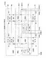
図1は、本発明の半導体メモリの第1の実施形態を示している。この半導体メモリは、シリコン基板上にCMOSプロセスを使用してスタティックランダムアクセスメモリ(以下、SRAMと称する)として形成されている。SRAMは、SOC(System On Chip)等のシステムLSIに搭載されるRAMマクロである。RAMマクロは、システムLSIの設計ツールの一つであるコンパイラにより生成される。SRAMは、メモリコアCORE、データ入出力部DIO(信号制御部)、デコード部DEC、動作制御部OPCおよび信号入力部SINを有している。 FIG. 1 shows a first embodiment of the semiconductor memory of the present invention. This semiconductor memory is formed as a static random access memory (hereinafter referred to as SRAM) using a CMOS process on a silicon substrate. The SRAM is a RAM macro mounted on a system LSI such as an SOC (System On Chip). The RAM macro is generated by a compiler that is one of the design tools for the system LSI. The SRAM includes a memory core CORE, a data input / output unit DIO (signal control unit), a decoding unit DEC, an operation control unit OPC, and a signal input unit SIN.
メモリコアCOREは、一対のセルアレイCARY、ICARYおよび読み書き制御部RWCとを有している。セルアレイCARY、ICARYは、図の縦方向に沿って配置されている。読み書き制御部RWCは、セルアレイCARY、ICARYの間に配置されている。読み書き制御部RWCは、セルアレイCARY、ICARYに共通の回路であり、セルアレイCARY、ICARYに対するデータの読み書きを制御する。読み書き制御部RWCは、読み出しグローバルビット線RGBLおよび書き込みグローバルビット線WGBL、WGBLXを介してデータ入出力部DIOに接続されている。 The memory core CORE has a pair of cell arrays CARY and ICARY and a read / write control unit RWC. The cell arrays CARY and ICARY are arranged along the vertical direction in the figure. The read / write controller RWC is arranged between the cell arrays CARY and ICARY. The read / write controller RWC is a circuit common to the cell arrays CARY and ICARY, and controls reading and writing of data with respect to the cell arrays CARY and ICARY. The read / write control unit RWC is connected to the data input / output unit DIO via the read global bit line RGBL and the write global bit lines WGBL, WGBLX.
セルアレイCARY、ICARYは、マトリックス状に配置された複数のスタティックメモリセルMCと、メモリセルMCに接続されたワード線WLおよび相補のビット線BL
、BLXとを有している。すなわち、このSRAMでは、メモリセルMCに読み書きされるデータの伝達経路は、ビット線BL、BLXとグローバルビット線RGBL、WGBL、WGBLXに階層化されている。The cell arrays CARY and ICARY include a plurality of static memory cells MC arranged in a matrix, word lines WL connected to the memory cells MC, and complementary bit lines BL.
, BLX. In other words, in this SRAM, the transmission path of data read / written to / from the memory cell MC is hierarchized into bit lines BL and BLX and global bit lines RGBL, WGBL and WGBLX.
セルアレイCARYは、基本の記憶容量を有する完全セルアレイである。例えば、セルアレイCARYの記憶容量は8kビットである。セルアレイICARYは、基本の記憶容量より小さい記憶容量を有する不完全セルアレイである。例えば、セルアレイICARYの記憶容量は4kビットである。この実施形態では、例えば、システムLSIを設計するユーザは、12kビットのSRAMを必要としている。コンパイラは、SRAMを、8kビットの完全セルアレイCARYと4kビットの不完全セルアレイICARYで構成する。 The cell array CARY is a complete cell array having a basic storage capacity. For example, the storage capacity of the cell array CARY is 8k bits. The cell array ICARY is an incomplete cell array having a storage capacity smaller than the basic storage capacity. For example, the storage capacity of the cell array ICARY is 4k bits. In this embodiment, for example, a user who designs a system LSI needs a 12-kbit SRAM. The compiler configures the SRAM with an 8 kbit complete cell array CARY and a 4 kbit incomplete cell array ICARY.
コンパイラは、セルアレイICARYをデータ入出力部DIOの近くに配置し、セルアレイCARYをデータ入出力部DIOの遠くに配置する。セルアレイCARY、ICARYをアクセスするためのロウアドレスRADは、データ入出力部DIOに最も遠い位置からデータ入出力部DIOに向けて昇順に割り当てられる。このように、この実施形態では、セルアレイICARYに割り当てられたアドレスは、最大のロウアドレスRAD191を含んでいる。ロウアドレスRADは、ワード線WLを示すアドレスであり、ワード線WLを選択するためにアドレス信号ADとしてSRAMの外部から供給される。 The compiler arranges the cell array ICARY near the data input / output unit DIO and the cell array CARY far from the data input / output unit DIO. Row addresses RAD for accessing the cell arrays CARY and ICARY are assigned in ascending order from the position farthest to the data input / output unit DIO to the data input / output unit DIO. Thus, in this embodiment, the address assigned to the cell array ICARY includes the maximum row address RAD191. The row address RAD is an address indicating the word line WL, and is supplied from the outside of the SRAM as an address signal AD for selecting the word line WL.
データ入出力部DIOに遠いセルアレイCARYからセルアレイICARYに向けてアドレスを昇順に割り当てることで、アドレスADをデコードするデコード部DECの回路設計を容易にできる。換言すれば、ユーザ仕様に応じてRAMマクロを生成するコンパイラのプログラムを、従来のプログラムを利用して簡易に設計できる。また、アドレスが順序正しく割り当てているため、SRAMに不良が発生したときに、不良アドレスを物理的に特定しやすい。したがって、不良解析の効率を向上できる。 By assigning addresses in ascending order from the cell array CARY far from the data input / output unit DIO to the cell array ICARY, the circuit design of the decoding unit DEC that decodes the address AD can be facilitated. In other words, a compiler program that generates a RAM macro according to user specifications can be easily designed using a conventional program. In addition, since the addresses are assigned in order, it is easy to physically identify the defective address when a failure occurs in the SRAM. Therefore, the efficiency of failure analysis can be improved.
セルアレイCARYでは、一対のビット線BL、BLXに128個のメモリセルMCが接続されている(RAD=0−127)。すなわち、128個のメモリセルMCが、図の縦方向に並んでいる。一方、セルアレイICARYでは、一対のビット線BL、BLXに64個のメモリセルMCが接続されている(RAD=128−191)。すなわち、64個のメモリセルMCが、図の縦方向に並んでいる。したがって、セルアレイICARYのビット線方向の長さは、セルアレイCARYのビット線方向の長さのほぼ半分である。 In the cell array CARY, 128 memory cells MC are connected to a pair of bit lines BL and BLX (RAD = 0 to 127). That is, 128 memory cells MC are arranged in the vertical direction in the figure. On the other hand, in the cell array ICARY, 64 memory cells MC are connected to a pair of bit lines BL and BLX (RAD = 128-191). That is, 64 memory cells MC are arranged in the vertical direction in the figure. Therefore, the length of the cell array ICARY in the bit line direction is almost half of the length of the cell array CARY in the bit line direction.
また、セルアレイCARY、ICARYでは、1本のワード線WLに64個のメモリセルMCが接続されている。すなわち、64個のメモリセルMCが、図の横方向に並んでいる。例えば、データ出力端子DOUTおよびデータ入力端子DINは、64ビットを有している。このため、読み出し動作において、ワード線WLの選択によりデータ入出力部DIOに読み出された64ビットの読み出しデータが、データ出力端子DOUTに同時に出力される。同様に、書き込み動作において、64ビットの書き込みデータは、ロウアドレスRADで選択される64個のメモリセルMCに同時に書き込まれる。 In the cell arrays CARY and ICARY, 64 memory cells MC are connected to one word line WL. That is, 64 memory cells MC are arranged in the horizontal direction in the figure. For example, the data output terminal DOUT and the data input terminal DIN have 64 bits. Therefore, in the read operation, 64-bit read data read to the data input / output unit DIO by selecting the word line WL is simultaneously output to the data output terminal DOUT. Similarly, in the write operation, 64-bit write data is simultaneously written into the 64 memory cells MC selected by the row address RAD.
データ入出力部DIOは、セルアレイCARY、ICARYの列の外部端子DOUT、DIN側に配置されている。データ入出力部DIOは、読み出し動作時に、メモリセルMCから読み出されるデータを読み出しグローバルビット線RGBLを介して受け、受けたデータをデータ出力端子DOUTに出力する。また、データ入出力部DIOは、書き込み動作時に、データ入力端子DINに供給される書き込みデータを相補のデータに変換し、変換したデータを書き込みグローバルビット線WGBL、WGBLXを介してメモリコアCOREに出力する。この実施形態では、読み出し用の外部データ端子DOUTと、書き込み用の外部データ端子DINとを独立して形成しているが、読み出しおよび書き込みに
共通の外部データ端子を形成してもよい。The data input / output unit DIO is arranged on the external terminals DOUT, DIN side of the columns of the cell arrays CARY, ICARY. During the read operation, the data input / output unit DIO receives data read from the memory cell MC via the read global bit line RGBL, and outputs the received data to the data output terminal DOUT. In addition, the data input / output unit DIO converts the write data supplied to the data input terminal DIN into complementary data during a write operation, and outputs the converted data to the memory core CORE via the write global bit lines WGBL and WGBLX. To do. In this embodiment, the external data terminal DOUT for reading and the external data terminal DIN for writing are formed independently. However, a common external data terminal for reading and writing may be formed.
読み書き制御部RWCは、読み出し動作において、ビット線BLに読み出されたデータを増幅し、増幅したデータを読み出しグローバルビット線RGBLに出力する。読み書き制御部RWCは、書き込み動作において、書き込みグローバルビット線WGBL、WGBLXに供給される相補の書き込みデータをビット線BL、BLXに出力する。 In the read operation, the read / write control unit RWC amplifies the data read to the bit line BL and reads the amplified data to the global bit line RGBL. In the write operation, the read / write controller RWC outputs complementary write data supplied to the write global bit lines WGBL and WGBLX to the bit lines BL and BLX.
この実施形態では、グローバルビット線RGBL、WGBL、WGBLXは、セルアレイICARY上に配線されている。グローバルビット線RGBL、WGBL、WGBLXの長さは、セルアレイCARY上に配線する場合に比べて短くできる。このため、グローバルビット線RGBL、WGBL、WGBLXの負荷容量を小さくできる。したがって、読み出し動作時および書き込み動作時の充放電電流を削減できる。また、読み出しデータおよび書き込みデータが、データ入出力部DIOと読み書き制御部RWC間に伝達される時間を短くできる。この結果、SRAMの動作時の消費電力を削減でき、アクセス時間(読み出し動作時間および書き込み動作時間)を短縮できる。特に、半導体メモリでは、多数のグローバルビット線RGBL、WGBL、WGBLXが、セルアレイCARY、ICARY上に配線される(この例では、192本)。このため、消費電力の削減効果は大きい。 In this embodiment, the global bit lines RGBL, WGBL, WGBLX are wired on the cell array ICARY. The length of the global bit lines RGBL, WGBL, WGBLX can be shortened compared to the case of wiring on the cell array CARY. For this reason, the load capacity of the global bit lines RGBL, WGBL, WGBLX can be reduced. Therefore, the charge / discharge current during the read operation and the write operation can be reduced. Further, it is possible to shorten the time during which read data and write data are transmitted between the data input / output unit DIO and the read / write control unit RWC. As a result, power consumption during operation of the SRAM can be reduced, and access time (read operation time and write operation time) can be shortened. In particular, in the semiconductor memory, a large number of global bit lines RGBL, WGBL, WGBLX are wired on the cell arrays CARY, ICARY (192 in this example). For this reason, the reduction effect of power consumption is great.
デコード部DECは、読み出し動作中および書き込み動作中に、動作制御部OPCからのタイミング信号に同期してアドレス信号AD(=ロウアドレスRAD)をデコードし、アドレス信号ADに対応するワード線WLを高レベルに活性化する。また、デコード部DECは、書き込み動作中に、動作制御部OPCからのタイミング信号に同期してアドレス信号AD(=ロウアドレスRAD)をデコードし、アドレス信号ADに対応する書き込み制御信号WEC(図2に示すWEC0−1)を高レベルに活性化する。書き込み制御信号WECの活性化により、書き込みグローバルビット線WGBL、WGBLXは、一方のセルアレイCARY、ICARYのビット線BL、BLXに接続される。 During the read operation and the write operation, the decode unit DEC decodes the address signal AD (= row address RAD) in synchronization with the timing signal from the operation control unit OPC, and sets the word line WL corresponding to the address signal AD to the high level. Activate to level. Further, during the write operation, the decode unit DEC decodes the address signal AD (= row address RAD) in synchronization with the timing signal from the operation control unit OPC, and the write control signal WEC corresponding to the address signal AD (FIG. 2). WEC0-1) is activated to a high level. By the activation of the write control signal WEC, the write global bit lines WGBL and WGBLX are connected to the bit lines BL and BLX of one of the cell arrays CARY and ICARY.
動作制御部OPCは、信号入力部SINを介して供給されるライトイネーブル信号WEおよびチップセレクト信号CSに応じて読み出し要求および書き込み要求を検出し、検出した要求に応じてSRAMの読み出し動作および書き込み動作を制御するためのタイミング信号を生成する。生成されたタイミング信号は、デコード部DECおよびデータ入出力部DIO等に出力される。例えば、動作制御部OPCは、読み出し動作時におよび書き込み動作時に、ワード線WLの活性化期間を設定するワード線活性化タイミング信号を出力する。動作制御部OPCは、読み出し動作および書き込み動作が実行されないスタンバイ期間に、読み出しグローバルビット線RGBLを高レベルにプリチャージするために、プリチャージ信号PCXを低レベルに活性化する。 The operation control unit OPC detects a read request and a write request according to the write enable signal WE and the chip select signal CS supplied via the signal input unit SIN, and reads and writes the SRAM according to the detected request. A timing signal for controlling the signal is generated. The generated timing signal is output to the decoding unit DEC, the data input / output unit DIO, and the like. For example, the operation control unit OPC outputs a word line activation timing signal that sets an activation period of the word line WL during a read operation and a write operation. The operation control unit OPC activates the precharge signal PCX to a low level in order to precharge the read global bit line RGBL to a high level during a standby period when the read operation and the write operation are not performed.
信号入力部SINは、外部端子に供給されるライトイネーブル信号WE、チップセレクト信号CSおよびアドレス信号ADを、クロック信号CLKに同期して受信し、受信した信号を動作制御部OPCおよびデコード部DECに出力する。信号入力部SINは、チップセレクト信号CSが活性化されている間、書き込みイネーブル信号WEが低レベルのとき読み出し要求を検出し、ライトネーブル信号WEが高レベルのとき書き込み要求を検出する。 The signal input unit SIN receives the write enable signal WE, the chip select signal CS, and the address signal AD supplied to the external terminals in synchronization with the clock signal CLK, and receives the received signals to the operation control unit OPC and the decoding unit DEC. Output. While the chip select signal CS is activated, the signal input unit SIN detects a read request when the write enable signal WE is at a low level, and detects a write request when the write enable signal WE is at a high level.
図2は、図1に示したメモリコアCOREの詳細を示している。セルアレイCARY、ICARYは、上述したように、マトリックス状に配置され、相補のビット線BL、BLXおよびワード線WLに接続された複数のスタティックメモリセルMCを有している。 FIG. 2 shows details of the memory core CORE shown in FIG. As described above, the cell arrays CARY and ICARY have a plurality of static memory cells MC arranged in a matrix and connected to complementary bit lines BL and BLX and word lines WL.
読み書き制御部RWCは、センスアンプSA、プリチャージ回路PREおよび書き込み
スイッチWSWを有している。センスアンプSAは、入力がセルアレイCARY、ICARYのビット線BLに接続された2入力NANDゲート(負論理のオア回路)と、ゲートがNANDゲートの出力に接続されたnMOSトランジスタとを有している。nMOSトランジスタは、ソースが接地線VSSに接続され、ドレインが読み出しグローバルビット線RGBLに接続されている。このように、センスアンプSAは、セルアレイCARY、ICARYに共有されている。センスアンプSAは、ビット線BLに読み出されたデータの信号量を増幅し、データの論理を判定する。具体的には、読み出し動作において、メモリセルMCからビット線BLに低レベル(論理0)が読み出されるとき、NANDゲートは、高レベルを出力する。センスアンプSAのnMOSトランジスタはオンし、読み出しグローバルビット線RGBLは、高レベルから低レベルに変化する。読み出し動作において、メモリセルMCからビット線BLに高レベル(論理1)が読み出されるとき、nMOSトランジスタはオフする。このため、読み出しグローバルビット線RGBLは、高レベルに保持される。The read / write control unit RWC includes a sense amplifier SA, a precharge circuit PRE, and a write switch WSW. The sense amplifier SA has a two-input NAND gate (negative logic OR circuit) whose inputs are connected to the bit lines BL of the cell arrays CARY and ICARY, and an nMOS transistor whose gate is connected to the output of the NAND gate. . The nMOS transistor has a source connected to the ground line VSS and a drain connected to the read global bit line RGBL. Thus, the sense amplifier SA is shared by the cell arrays CARY and ICARY. The sense amplifier SA amplifies the signal amount of the data read to the bit line BL and determines the data logic. Specifically, in a read operation, when a low level (logic 0) is read from the memory cell MC to the bit line BL, the NAND gate outputs a high level. The nMOS transistor of the sense amplifier SA is turned on, and the read global bit line RGBL changes from a high level to a low level. In a read operation, when a high level (logic 1) is read from the memory cell MC to the bit line BL, the nMOS transistor is turned off. For this reason, the read global bit line RGBL is held at a high level.
プリチャージ回路PREは、ゲートでプリチャージ信号PCXを受けるpMOSトランジスタを有している。pMOSトランジスタは、ソースが電源線VDDに接続され、ドレインが読み出しグローバルビット線RGBLに接続されている。プリチャージ回路PREは、読み出し動作および書き込み動作が実行されないスタンバイ期間に、読み出しグローバルビット線RGBLを高レベル(VDD)にプリチャージするために、低レベルのプリチャージ信号PCXを受けてオンする。 The precharge circuit PRE has a pMOS transistor that receives a precharge signal PCX at its gate. The pMOS transistor has a source connected to the power supply line VDD and a drain connected to the read global bit line RGBL. The precharge circuit PRE is turned on in response to a low-level precharge signal PCX in order to precharge the read global bit line RGBL to a high level (VDD) during a standby period when the read operation and the write operation are not performed.
書き込みスイッチWSWは、書き込みグローバルビット線WGBLをビット線BLに接続するnMOSトランジスタと、書き込みグローバルビット線WGBLXをビット線BLXに接続するnMOSトランジスタとを有している。セルアレイCARYが書き込み動作を実行するとき、セルアレイCARYのビット線BL、BLXに接続された書き込みスイッチWSWが、書き込み制御信号WEC1に応じてオンする。同様に、セルアレイICARYが書き込み動作を実行するとき、セルアレイICARYのビット線BL、BLXに接続された書き込みスイッチWSWが、書き込み制御信号WEC0に応じてオンする。 The write switch WSW includes an nMOS transistor that connects the write global bit line WGBL to the bit line BL, and an nMOS transistor that connects the write global bit line WGBLX to the bit line BLX. When the cell array CARY performs a write operation, the write switch WSW connected to the bit lines BL and BLX of the cell array CARY is turned on according to the write control signal WEC1. Similarly, when the cell array ICARY performs a write operation, the write switch WSW connected to the bit lines BL and BLX of the cell array ICARY is turned on according to the write control signal WEC0.
図3は、図2に示したメモリセルMCの詳細を示している。各メモリセルMCは、一対のインバータを有し書き込みデータを保持するラッチと、ラッチの相補の記憶ノード(各インバータの出力ノード)にそれぞれ一端が接続された一対のトランスファトランジスタ(nMOSトランジスタ)とを有している。トランスファトランジスタの他端は、相補のビット線BL、BLXのいずれかに接続されている。トランスファトランジスタのゲートは、ワード線WLに接続されている。 FIG. 3 shows details of the memory cell MC shown in FIG. Each memory cell MC includes a latch having a pair of inverters and holding write data, and a pair of transfer transistors (nMOS transistors) each having one end connected to a complementary storage node (output node of each inverter) of the latch. Have. The other end of the transfer transistor is connected to one of complementary bit lines BL and BLX. The gate of the transfer transistor is connected to the word line WL.
図4は、第1の実施形態の比較例を示している。この例では、不完全セルアレイICARYは、データ入出力部DIOから遠い位置に配置されている。グローバルビット線RGBL、WGBL、WGBLXは、データ入出力部DIOに近い完全セルアレイCARY上に配線される。図4に示したSRAMは、図3に比べてグローバルビット線RGBL、WGBL、WGBLXが長いため、負荷容量は大きい。このため、SRAMの消費電力は増加し、アクセス時間も長くなる。 FIG. 4 shows a comparative example of the first embodiment. In this example, the incomplete cell array ICARY is arranged at a position far from the data input / output unit DIO. The global bit lines RGBL, WGBL, WGBLX are wired on the complete cell array CARY close to the data input / output unit DIO. The SRAM shown in FIG. 4 has a larger load capacity because the global bit lines RGBL, WGBL, WGBLX are longer than those in FIG. For this reason, the power consumption of the SRAM increases and the access time also becomes longer.
以上、第1の実施形態では、不完全セルアレイICARYを、完全セルアレイCARYよりデータ入出力部DIO側に配置することで、グローバルビット線RGBL、WGBL、WGBLXの配線長を短くできる。したがって、グローバルビット線RGBL、WGBL、WGBLXの負荷容量を削減でき、セルアレイICARY、CARYの動作時に発生するグローバル線の充放電電流を削減できる。この結果、SRAMの消費電力を削減でき、SRAMのアクセス時間を短縮できる。本発明を、ユーザ仕様に応じて記憶容量が設定可能なRAMマクロに適用することで、RAMマクロが搭載されるチップの消費電力を、
ユーザ毎に最小限に抑えることが可能になる。As described above, in the first embodiment, the wiring length of the global bit lines RGBL, WGBL, WGBLX can be shortened by disposing the incomplete cell array ICARY closer to the data input / output unit DIO than the complete cell array CARY. Therefore, the load capacity of the global bit lines RGBL, WGBL, WGBLX can be reduced, and the charge / discharge current of the global line generated during the operation of the cell arrays ICARY, CARY can be reduced. As a result, the power consumption of the SRAM can be reduced and the access time of the SRAM can be shortened. By applying the present invention to a RAM macro whose storage capacity can be set according to user specifications, the power consumption of the chip on which the RAM macro is mounted can be reduced.
It becomes possible to minimize to each user.
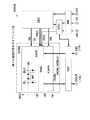
図5は、本発明の半導体メモリの第2の実施形態を示している。第1の実施形態で説明した要素と同一の要素については、同一の符号を付し、これ等については、詳細な説明を省略する。この実施形態のSRAMは、メモリコアCOREの記憶容量および構造が第1の実施形態と異なっている。これに伴い、アドレスADのビット数が増えるため、デコード部DEC等が第1の実施形態と相違する。但し、各回路ブロックの基本的な機能は、第1の実施形態と同じである。 FIG. 5 shows a second embodiment of the semiconductor memory of the present invention. The same elements as those described in the first embodiment are denoted by the same reference numerals, and detailed description thereof will be omitted. The SRAM of this embodiment is different from the first embodiment in the storage capacity and structure of the memory core CORE. Accordingly, the number of bits of the address AD increases, so that the decoding unit DEC and the like are different from the first embodiment. However, the basic functions of each circuit block are the same as those in the first embodiment.
メモリコアCOREは、一対のメモリユニットMU0、MU1を有している。メモリユニットMU0は、完全セルアレイCARYと、不完全セルアレイICARYと、セルアレイCARY、ICARYの間に配置された読み書き制御部RWCとを有している。メモリユニットMU0において、不完全セルアレイICARYは、完全セルアレイCARYよりデータ入出力部DIO側に配置されている。すなわち、不完全セルアレイICARYは、メモリユニットMU0の読み書き制御部RWCに対してデータ入出力部DIO側に配置されている。 The memory core CORE has a pair of memory units MU0 and MU1. The memory unit MU0 includes a complete cell array CARY, an incomplete cell array ICARY, and a read / write control unit RWC arranged between the cell arrays CARY and ICARY. In the memory unit MU0, the incomplete cell array ICARY is arranged closer to the data input / output unit DIO than the complete cell array CARY. That is, the incomplete cell array ICARY is arranged on the data input / output unit DIO side with respect to the read / write control unit RWC of the memory unit MU0.
メモリユニットMU1は、一対の完全セルアレイCARYと、これ等完全セルアレイCARYの間に配置された読み書き制御部RWCとを有している。メモリユニットMU0は、メモリユニットMU1に比べて、データ入出力部DIOに近い位置に配置されている。 The memory unit MU1 includes a pair of complete cell arrays CARY and a read / write control unit RWC arranged between these complete cell arrays CARY. The memory unit MU0 is disposed closer to the data input / output unit DIO than the memory unit MU1.
この実施形態では、例えば、システムLSIを設計するユーザは、28kビットのSRAMを必要としている。メモリコアCOREは、3つの完全セルアレイCARY(8kビット)と1つの不完全セルアレイICARY(4kビット)で構成される。ロウアドレスRADは、データ入出力部DIOに最も遠い位置からデータ入出力部DIOに向けて昇順に割り当てられる。セルアレイICARYに割り当てられたアドレスは、最大のロウアドレスRAD447を含んでいる。第1の実施形態と同様に、データ入出力部DIOに遠いセルアレイCARYからセルアレイICARYに向けてアドレスを昇順に割り当てることで、アドレスADをデコードするデコード部DECの回路設計を容易にできる。換言すれば、ユーザ仕様に応じてRAMマクロを生成するコンパイラのプログラムを、従来のプログラムを利用して簡易に設計できる。また、アドレスが順序正しく割り当てているため、不良アドレスを物理的に特定しやすく、不良解析の効率を向上できる。 In this embodiment, for example, a user designing a system LSI needs a 28-kbit SRAM. The memory core CORE is composed of three complete cell arrays CARY (8k bits) and one incomplete cell array ICARY (4k bits). The row address RAD is assigned in ascending order from the position farthest to the data input / output unit DIO toward the data input / output unit DIO. The address assigned to the cell array ICARY includes the maximum row address RAD447. Similar to the first embodiment, by assigning addresses in ascending order from the cell array CARY far from the data input / output unit DIO to the cell array ICARY, the circuit design of the decoding unit DEC that decodes the address AD can be facilitated. In other words, a compiler program that generates a RAM macro according to user specifications can be easily designed using a conventional program. Further, since the addresses are assigned in order, it is easy to physically identify the defective address, and the efficiency of defect analysis can be improved.
読み出しグローバルビット線RGBLおよび書き込みグローバルビット線WGBL、WGBLXは、メモリユニットMU0−1の読み書き制御部RWCに接続されている。読み書き制御部RWCの回路構成は、上述した図2と同じである。グローバルビット線RGBL、WGBL、WGBLXは、2つの完全セルアレイCARY上と、不完全セルアレイICARY上を配線されている。グローバルビット線RGBL、WGBL、WGBLXを不完全セルアレイICARY上に配線することで、第1の実施形態と同様に、グローバルビット線RGBL、WGBL、WGBLXの配線長は短くなる。したがって、SRAMの消費電力を削減でき、アクセス時間を短縮できる。 The read global bit line RGBL and the write global bit lines WGBL, WGBLX are connected to the read / write control unit RWC of the memory units MU0-1. The circuit configuration of the read / write control unit RWC is the same as that in FIG. The global bit lines RGBL, WGBL, WGBLX are wired on the two complete cell arrays CARY and the incomplete cell array ICARY. By wiring the global bit lines RGBL, WGBL, WGBLX on the incomplete cell array ICARY, the wiring length of the global bit lines RGBL, WGBL, WGBLX is shortened as in the first embodiment. Therefore, the power consumption of the SRAM can be reduced and the access time can be shortened.
図6は、第2の実施形態の比較例を示している。上述した図4と同様に、この例では、不完全セルアレイICARYは、データ入出力部DIOから遠い位置に配置されている。このため、グローバルビット線RGBL、WGBL、WGBLXは、3つの完全セルアレイCARY上に配線され、不完全セルアレイICARY上に配線されない。グローバルビット線RGBL、WGBL、WGBLXの負荷容量が大きくなるため、SRAMの消費電力は増加し、アクセス時間も長くなる。 FIG. 6 shows a comparative example of the second embodiment. Similar to FIG. 4 described above, in this example, the incomplete cell array ICARY is arranged at a position far from the data input / output unit DIO. For this reason, the global bit lines RGBL, WGBL, WGBLX are wired on the three complete cell arrays CARY and not on the incomplete cell array ICARY. Since the load capacity of the global bit lines RGBL, WGBL, WGBLX increases, the power consumption of the SRAM increases and the access time also increases.
以上、第2の実施形態においても、上述した第1の実施形態と同様の効果を得ることが
できる。さらに、複数の完全セルアレイCARYと1つの不完全セルアレイICARYとを有するSRAMにおいても、グローバルビット線RGBL、WGBL、WGBLXの充放電電流を削減でき、SRAMの消費電力を削減できる。また、SRAMのアクセス時間を短縮できる。As mentioned above, also in 2nd Embodiment, the effect similar to 1st Embodiment mentioned above can be acquired. Furthermore, even in an SRAM having a plurality of complete cell arrays CARY and one incomplete cell array ICARY, the charge / discharge current of the global bit lines RGBL, WGBL, WGBLX can be reduced, and the power consumption of the SRAM can be reduced. Further, the SRAM access time can be shortened.
図7は、本発明の半導体メモリの第3の実施形態を示している。第1および第2の実施形態で説明した要素と同一の要素については、同一の符号を付し、これ等については、詳細な説明を省略する。この実施形態のSRAMは、メモリコアCOREの構造が第2の実施形態と異なっている。具体的には、不完全セルアレイICARYの位置と、読み出しグローバルビット線RGBLおよび書き込みグローバルビット線WGBL、WGBLXの構造が、第2の実施形態と異なっている。リピータ回路RRP、WRPが、読み書き制御回路RWC内に形成されている。その他の構成は、第2の実施形態(図5)と同じである。 FIG. 7 shows a third embodiment of the semiconductor memory of the present invention. The same elements as those described in the first and second embodiments are denoted by the same reference numerals, and detailed description thereof will be omitted. The SRAM of this embodiment is different from the second embodiment in the structure of the memory core CORE. Specifically, the position of the incomplete cell array ICARY and the structure of the read global bit line RGBL and the write global bit lines WGBL and WGBLX are different from those of the second embodiment. Repeater circuits RRP and WRP are formed in the read / write control circuit RWC. Other configurations are the same as those of the second embodiment (FIG. 5).
読み出しグローバルビット線RGBLは、一対の読み出しサブグローバルビット線RSGBL0−1をリピータ回路RRPにより接続することで形成されている。書き込みグローバルビット線WGBL、WGBLXは、一対の書き込みサブグローバルビット線WSGBL0−1および一対の書き込みサブグローバルビット線WSGBLX0−1をリピータ回路WRPにより接続することで形成されている。 The read global bit line RGBL is formed by connecting a pair of read sub-global bit lines RSGBL0-1 by a repeater circuit RRP. The write global bit lines WGBL and WGBLX are formed by connecting a pair of write subglobal bit lines WSGBL0-1 and a pair of write subglobal bit lines WSGBLBX0-1 by a repeater circuit WRP.
リピータ回路RRP、WRPの形成により、データ入出力部DIOに近いメモリユニットMU0がアクセスされるときに、メモリユニットMU1に対応するサブグローバルビット線RSGBL、WSGBL、WSGBLXを、グローバルビット線RGBL、WGBL、WGBLXから切り離すことができる。これにより、グローバルビット線RGBL、WGBL、WGBLXの負荷容量が減るため、アクセス時の消費電力を削減できる。また、アクセス時間を短縮できる。 By forming the repeater circuits RRP and WRP, when the memory unit MU0 close to the data input / output unit DIO is accessed, the sub-global bit lines RSGBL, WSGBL, WSGBLB corresponding to the memory unit MU1 are connected to the global bit lines RGBL, WGBL, Can be disconnected from WGBLX. As a result, the load capacity of the global bit lines RGBL, WGBL, WGBLX is reduced, so that power consumption during access can be reduced. Also, the access time can be shortened.
この実施形態では、メモリユニットMU0−1のワード線WLの本数は、それぞれ256本、192本である。このため、SRAMがランダムアクセスされる場合、メモリユニットMU0−1がアクセスされる比率は、”4:3”である。一方、メモリユニットMU0がアクセスされるとき、サブグローバルビット線RSGBL0、WSGBL0、WSGBLX0のみが使用される。メモリユニットMU1がアクセスされるとき、サブグローバルビット線RSGBL0−1、WSGBL0−1、WSGBLX0−1が両方使用される。メモリユニットMU1がアクセスされるときの消費電力は、グローバルビット線RGBL、WGBL、WGBLXの充放電電流が増えるため、メモリユニットMU0がアクセスされるときの消費電力より大きくなる。 In this embodiment, the number of word lines WL in the memory units MU0-1 is 256 and 192, respectively. For this reason, when the SRAM is randomly accessed, the ratio of the memory units MU0-1 being accessed is “4: 3”. On the other hand, when the memory unit MU0 is accessed, only the subglobal bit lines RSGBL0, WSGBL0, WSGBLB0 are used. When the memory unit MU1 is accessed, both the sub-global bit lines RSGBL0-1, WSGBL0-1, WSGBLBX0-1 are used. The power consumption when the memory unit MU1 is accessed becomes larger than the power consumption when the memory unit MU0 is accessed because the charge / discharge currents of the global bit lines RGBL, WGBL, WGBLX are increased.
リピータ回路RRP、WRPが挿入されるSRAMにおいて、不完全セルアレイICARYをデータ入出力部DIOに最も遠い位置を除く位置に配置し、かつ、アクセス頻度の高いメモリユニットMU0(セルアレイICARYを含まないメモリユニット)をデータ入出力部DIOの近くに配置することで、グローバルビット線RGBL、WGBL、WGBLXの充放電電流を最小限にできる。この結果、SRAMのアクセス時の消費電力(平均値)を削減できる。 In the SRAM into which the repeater circuits RRP and WRP are inserted, the incomplete cell array ICARY is arranged at a position excluding the position farthest from the data input / output unit DIO, and the memory unit MU0 (memory unit not including the cell array ICARY) with high access frequency ) Is arranged near the data input / output unit DIO, the charge / discharge current of the global bit lines RGBL, WGBL, WGBLX can be minimized. As a result, the power consumption (average value) when accessing the SRAM can be reduced.
図8は、図7に示したメモリユニットMU0の詳細を示している。メモリユニットMU0の読み書き制御部RWCは、図2に示した読み書き制御部RWCにリピータ回路RRP、WRPを追加して構成されている。図8では、書き込み制御信号WEC0−1の記載を省略している。なお、メモリユニットMU1の読み書き制御部RWCは、図2と同じである。 FIG. 8 shows details of the memory unit MU0 shown in FIG. The read / write control unit RWC of the memory unit MU0 is configured by adding repeater circuits RRP and WRP to the read / write control unit RWC shown in FIG. In FIG. 8, description of the write control signals WEC0-1 is omitted. The read / write control unit RWC of the memory unit MU1 is the same as that in FIG.
リピータ回路RRPは、入力が読み出しサブグローバルビット線RSGBL1に接続さ
れたインバータと、ゲートがインバータの出力に接続されたnMOSトランジスタとを有している。nMOSトランジスタは、ソースが接地線VSSに接続され、ドレインが読み出しサブグローバルビット線RSGBL0に接続されている。メモリユニットMU0が読み出しアクセスされるとき、読み出しサブグローバルビット線RSGBL1は、高レベルにプリチャージされた状態を保持する。リピータ回路RRPのnMOSトランジスタはオフするため、読み出しサブグローバルビット線RSGBL1は、読み出しサブグローバルビット線RSGBL0から切り離される。一方、メモリユニットMU1が読み出しアクセスされるとき、リピータ回路RRPのnMOSトランジスタは、読み出しサブグローバルビット線RSGBL1の低レベルへの変化に応答してオンする。このため、読み出しサブグローバルビット線RSGBL1の論理レベルは、読み出しサブグローバルビット線RSGBL0に伝達される。The repeater circuit RRP has an inverter whose input is connected to the read subglobal bit line RSGBL1, and an nMOS transistor whose gate is connected to the output of the inverter. The nMOS transistor has a source connected to the ground line VSS and a drain connected to the read subglobal bit line RSGBL0. When the memory unit MU0 is read-accessed, the read subglobal bit line RSGBL1 holds a state precharged to a high level. Since the nMOS transistor of the repeater circuit RRP is turned off, the read subglobal bit line RSGBL1 is disconnected from the read subglobal bit line RSGBL0. On the other hand, when the memory unit MU1 is read-accessed, the nMOS transistor of the repeater circuit RRP is turned on in response to the change of the read subglobal bit line RSGBL1 to a low level. Therefore, the logic level of the read subglobal bit line RSGBL1 is transmitted to the read subglobal bit line RSGBL0.
リピータ回路WRPは、入力が書き込みサブグローバルビット線WSGBL0、WSGLBX0にそれぞれ接続された一対のインバータと、インバータの出力およびユニット選択信号USELをそれぞれ受ける一対の2入力NANDゲートとを有している。ユニット選択信号USELは、図7に示したデコード部DECにより生成される。デコード部DECは、アドレス信号ADに応じて、メモリユニットMU1が書き込みアクセスされるときにユニット選択信号USELを高レベルに変化する。このとき、リピータ回路WRPのNANDゲートは有効になり、書き込みサブグローバルビット線WSGBL0、WSGLBX0の論理レベルを書き込みサブグローバルビット線WSGBL1、WSGLBX1に伝達する。メモリユニットMU0が書き込みアクセスされる場合、ユニット選択信号USELは低レベルに保持される。このため、リピータ回路WRPのNANDゲートは、高レベル(VDD)を出力する。すなわち、書き込みサブグローバルビット線WSGBL1、WSGLBX1は、プリチャージレベルに保持される。 Repeater circuit WRP has a pair of inverters whose inputs are connected to write subglobal bit lines WSGBL0 and WSGLBX0, respectively, and a pair of two-input NAND gates that respectively receive the output of the inverter and unit selection signal USEL. The unit selection signal USEL is generated by the decoding unit DEC shown in FIG. The decode unit DEC changes the unit selection signal USEL to high level when the memory unit MU1 is accessed for writing in accordance with the address signal AD. At this time, the NAND gate of the repeater circuit WRP is enabled, and the logic levels of the write subglobal bit lines WSGBL0 and WSGLBX0 are transmitted to the write subglobal bit lines WSGBL1 and WSGLBX1. When the memory unit MU0 is accessed for writing, the unit selection signal USEL is held at a low level. For this reason, the NAND gate of the repeater circuit WRP outputs a high level (VDD). That is, the write subglobal bit lines WSGBL1 and WSGLBX1 are held at the precharge level.
図9は、第3の実施形態の第1の比較例を示している。不完全セルアレイICARYがデータ入出力部DIOから最も遠い位置に配置される場合、上述した図4と同様に、サブグローバルビット線RSGBL1、WSGBL1、WSGBLX1は、2つの完全セルアレイCARYを有するメモリユニットMU0上に配線される。このため、サブグローバルビット線RSGBL1、WSGBL1、WSGBLXは、図7に比べて長くなり、アクセス時の消費電力は増加する。 FIG. 9 shows a first comparative example of the third embodiment. When the incomplete cell array ICARY is arranged at the farthest position from the data input / output unit DIO, the subglobal bit lines RSGBL1, WSGBL1, WSGBLBX1 are located on the memory unit MU0 having two complete cell arrays CARY as in FIG. Wired to For this reason, the subglobal bit lines RSGBL1, WSGBL1, WSGBLBX become longer than those in FIG. 7, and the power consumption during access increases.
図10は、第3の実施形態の第2の比較例を示している。不完全セルアレイICARYがデータ入出力部DIOに最も近い位置に配置される場合、アクセス頻度の高いメモリユニットMU1がアクセスされるときに、サブグローバルビット線RSGBL1、WSGBL1、WSGBLX1が充放電される。このため、SRAMのアクセス時の消費電力(平均値)は増加する。 FIG. 10 shows a second comparative example of the third embodiment. When the incomplete cell array ICARY is arranged at a position closest to the data input / output unit DIO, the subglobal bit lines RSGBL1, WSGBL1, WSGBLBX1 are charged / discharged when the memory unit MU1 having a high access frequency is accessed. For this reason, the power consumption (average value) during SRAM access increases.
以上、第3の実施形態においても、上述した第1の実施形態と同様の効果を得ることができる。特に、グローバルビット線RGBL、WGBL、WGBLXが、サブグローバルビット線RSGBL0−1、WSGBL0−1、WSGBLX0−1で構成され、リピータ回路RRP、WRPが挿入される場合に、アクセス頻度の高いメモリユニットMU0の消費電力を下げることで、SRAMの消費電力を平均的に削減でき、半導体メモリのアクセス時間を壁金的に短縮できる。 As described above, also in the third embodiment, the same effect as in the first embodiment described above can be obtained. In particular, when the global bit lines RGBL, WGBL, WGBLX are composed of the sub-global bit lines RSGBL0-1, WSGBL0-1, WSGBLB0-1 and the repeater circuits RRP, WRP are inserted, the memory unit MU0 with high access frequency is inserted. The power consumption of the SRAM can be reduced on average, and the access time of the semiconductor memory can be shortened like a wall.
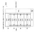
図11は、本発明の半導体メモリの第4の実施形態を示している。第1の実施形態で説明した要素と同一の要素については、同一の符号を付し、これ等については、詳細な説明を省略する。この実施形態のSRAMは、外部データ端子DOUT、DINがそれぞれ8ビットで構成されている。このため、読み出しグローバルビット線RGBLおよび書き込みグローバルビット線WGBL、WGBLXは、それぞれ8本ずつ配線されている。また
、読み書き制御部RWCが、第1の実施形態と相違する。FIG. 11 shows a fourth embodiment of the semiconductor memory of the present invention. The same elements as those described in the first embodiment are denoted by the same reference numerals, and detailed description thereof will be omitted. In the SRAM of this embodiment, the external data terminals DOUT and DIN are each composed of 8 bits. Therefore, eight read global bit lines RGBL and eight write global bit lines WGBL and WGBLX are wired. Further, the read / write control unit RWC is different from that of the first embodiment.
アドレス信号ADの下位3ビットは、64個のビット線対BL、BLXから8個のビット線対を選択するために、コラムアドレス信号として使用される。デコード部DECは、読み出し動作時に、コラムアドレス信号に応じて8本のコラム選択信号CL(図12に示すCL0−7)のいずれかを高レベルに活性化する。デコード部DECは、書き込み動作時に、コラムアドレス信号およびロウアドレス信号(アドレス信号ADの上位ビット)に応じて書き込み制御信号WEC(後述する16本のWECU、WECD)のいずれかを高レベルに活性化する。その他の構成は、第1の実施形態(図1)と同じである。 The lower 3 bits of the address signal AD are used as a column address signal in order to select 8 bit line pairs from 64 bit line pairs BL and BLX. During the read operation, the decode unit DEC activates any of the eight column selection signals CL (CL0-7 shown in FIG. 12) to a high level according to the column address signal. During the write operation, the decode unit DEC activates one of the write control signals WEC (16 WECUs and WECD, which will be described later) to a high level according to the column address signal and the row address signal (upper bits of the address signal AD). To do. Other configurations are the same as those of the first embodiment (FIG. 1).
図12は、図11に示した読み書き制御部RWCの詳細を示している。読み書き制御部RWCは、各センスアンプSAに接続されたコラムスイッチCSWを有している。各コラムスイッチCSWは、接地線とセンスアンプSAのnMOSトランジスタのソースとの間に接続されたnMOSトランジスタを有している。コラムスイッチCSWのnMOSトランジスタのゲートは、コラム選択信号線CL(CL0−7)のいずれかに接続されている。 FIG. 12 shows details of the read / write control unit RWC shown in FIG. The read / write controller RWC has a column switch CSW connected to each sense amplifier SA. Each column switch CSW has an nMOS transistor connected between the ground line and the source of the nMOS transistor of the sense amplifier SA. The gate of the nMOS transistor of the column switch CSW is connected to one of the column selection signal lines CL (CL0-7).
図12では、セルアレイCARYに配線される64本のビット線BLをBLU0−BLU63(図にはBLU0−10を記載)と示し、セルアレイICARYに配線される64本のビット線BLをBLD0−BLD63(図にはBLD0−10を記載)と示している。ビット線BLU0−7、BLD0−7に対応するコラムスイッチCSWは、コラム選択信号CL0−7を受けてそれぞれ動作する。同様に、ビット線BLU8−15、16−23、24−31、32−39、40−47、48−55、56−63およびビット線BLD8−15、16−23、24−31、32−39、40−47、48−55、56−63に対応するコラムスイッチCSWは、コラム選択信号CL0−7を受けてそれぞれ動作する。すなわち、コラムスイッチCSWは、読み出し動作時に、セルアレイCARY、ICARY毎に、ビット線BL0−63のいずれか8本を読み出しグローバルビット線RGBL0−7(図にはRGBL0−1を記載)にそれぞれ接続する。読み出しグローバルビット線RGBL0−7は、データ入出力部DIOを介してデータ端子DOUTに接続される。 In FIG. 12, 64 bit lines BL wired to the cell array CARY are shown as BLU0-BLU63 (BLU0-10 is shown in the figure), and 64 bit lines BL wired to the cell array ICARY are shown as BLD0-BLD63 ( The figure shows BLD0-10). The column switches CSW corresponding to the bit lines BLU0-7 and BLD0-7 operate in response to the column selection signal CL0-7. Similarly, bit lines BLU8-15, 16-23, 24-31, 32-39, 40-47, 48-55, 56-63 and bit lines BLD8-15, 16-23, 24-31, 32-39 , 40-47, 48-55, and 56-63 operate in response to the column selection signal CL0-7, respectively. That is, the column switch CSW reads out and connects any of the eight bit lines BL0-63 to the global bit lines RGBL0-7 (shown as RGBL0-1 in the figure) for each of the cell arrays CARY and ICARY during the read operation. . The read global bit lines RGBL0-7 are connected to the data terminal DOUT via the data input / output unit DIO.
なお、特に図示していないが、第1の実施形態と同様に、64個の書き込みスイッチWSWが、セルアレイCARY、ICARYに対応してそれぞれ形成されている。セルアレイCARYに対応する書き込みスイッチWSWのゲートは、書き込み制御信号WECU0−7のいずれかを受けている。セルアレイICARYに対応する書き込みスイッチWSWのゲートは、書き込み制御信号WECD0−7のいずれかを受けている。書き込み動作時、書き込み制御信号WECU0−7、WECD0−7のいずれかが高レベルに活性化される。そして、メモリコアCORE内の8組のビット線対BL、BLXが、書き込みグローバルビット線WGBL0−7、WGBLX0−7にそれぞれ接続される。 Although not particularly illustrated, 64 write switches WSW are formed corresponding to the cell arrays CARY and ICARY, respectively, as in the first embodiment. The gate of the write switch WSW corresponding to the cell array CARY receives one of the write control signals WECU0-7. The gate of the write switch WSW corresponding to the cell array ICARY receives one of the write control signals WECD0-7. During the write operation, one of the write control signals WECU0-7 and WECD0-7 is activated to a high level. The eight bit line pairs BL and BLX in the memory core CORE are connected to the write global bit lines WGBL0-7 and WGBLX0-7, respectively.
以上、第4の実施形態においても、上述した第1の実施形態と同様の効果を得ることができる。さらに、読み出しグローバルビット線RGBLおよび書き込みグローバルビット線WGBL、WGBLXに接続されるビット線BL、BLXを、コラムスイッチCSWおよび書き込みスイッチWSWにより選択するタイプのSRAMにおいても、グローバルビット線RGBL、WGBL、WGBLXの充放電電流を削減でき、消費電力を削減できる。また、SRAMのアクセス時間を短縮できる。 As described above, also in the fourth embodiment, the same effect as that of the above-described first embodiment can be obtained. Further, in the SRAM of the type in which the bit line BL, BLX connected to the read global bit line RGBL and the write global bit line WGBL, WGBLX is selected by the column switch CSW and the write switch WSW, the global bit lines RGBL, WGBL, WGBLX Charging / discharging current can be reduced, and power consumption can be reduced. Further, the SRAM access time can be shortened.
なお、上述した第2および第3の実施形態では、本発明を、2つのメモリユニットMU0−1を有するSRAMに適用する例について述べた。しかし、図12に示すように、本発明を、4つあるいはそれ以上のメモリユニットMUを有するSRAMに適用してもよい
。さらに、リピータ回路RRP、WRPが挿入されない場合、不完全セルアレイICARYは、任意のメモリユニットMUに形成できる。この際、不完全セルアレイICARYは、メモリユニットMU内において、読み書き制御回路RWCのデータ入出力部DIOに配置される。In the second and third embodiments described above, an example in which the present invention is applied to an SRAM having two memory units MU0-1 has been described. However, as shown in FIG. 12, the present invention may be applied to an SRAM having four or more memory units MU. Further, when the repeater circuits RRP and WRP are not inserted, the incomplete cell array ICARY can be formed in an arbitrary memory unit MU. At this time, the incomplete cell array ICARY is arranged in the data input / output unit DIO of the read / write control circuit RWC in the memory unit MU.
上述した実施形態では、本発明を、読み書き制御部RWCが一対のセルアレイCARY(またはICARY)で共有されるSRAMに適用する例について述べた。しかし、図14に示すように、本発明を、読み書き制御部RWCが各セルアレイCARY(またはICARY)毎に形成されるSRAMに適用してもよい。 In the above-described embodiment, the example in which the present invention is applied to an SRAM in which the read / write control unit RWC is shared by a pair of cell arrays CARY (or ICARY) has been described. However, as shown in FIG. 14, the present invention may be applied to an SRAM in which the read / write control unit RWC is formed for each cell array CARY (or ICARY).
上述した実施形態では、本発明の適用により、グローバルビット線RGBL、WGBL、WGBLXの充放電電流を削減する例について述べた。しかし、他の信号線の充放電電流を削減することで、SRAMの消費電力を削減することも可能である。例えば、データ端子のビット毎にデータの読み出しと書き込みとを指定できるパーシャルライト仕様を有するSRAMでは、データが書き込まれるビットに対応するセンスアンプを非活性化するためのセンスアンプマスク信号が、ビット線BL、BLXに平行に配線される。この場合に、センスアンプマスク信号が伝達される信号線の充放電電流を削減できる。一般に、本発明の適用により、ビット線BL、BLXに平行に、読み書き制御部RWCまで配線される信号線の充放電電流を削減でき、半導体メモリの動作時の消費電力を削減できる。 In the above-described embodiment, the example in which the charge / discharge current of the global bit lines RGBL, WGBL, WGBLX is reduced by applying the present invention has been described. However, it is also possible to reduce the power consumption of the SRAM by reducing the charge / discharge current of other signal lines. For example, in an SRAM having a partial write specification that can specify reading and writing of data for each bit of a data terminal, a sense amplifier mask signal for deactivating a sense amplifier corresponding to a bit to which data is written is a bit line. Wired in parallel to BL and BLX. In this case, the charge / discharge current of the signal line to which the sense amplifier mask signal is transmitted can be reduced. In general, by applying the present invention, it is possible to reduce the charge / discharge current of signal lines wired to the read / write control unit RWC in parallel with the bit lines BL and BLX, and to reduce power consumption during operation of the semiconductor memory.
上述した実施形態では、本発明を、SRAMに適用する例について述べた。しかし、本発明は、DRAM、擬似SRAMなどの他の半導体メモリにも適用できる。 In the above-described embodiment, the example in which the present invention is applied to the SRAM has been described. However, the present invention can also be applied to other semiconductor memories such as DRAM and pseudo SRAM.
以上、本発明について詳細に説明してきたが、上記の実施形態およびその変形例は発明の一例に過ぎず、本発明はこれに限定されるものではない。本発明を逸脱しない範囲で変形可能であることは明らかである。 As mentioned above, although this invention was demonstrated in detail, said embodiment and its modification are only examples of this invention, and this invention is not limited to this. Obviously, modifications can be made without departing from the scope of the present invention.
本発明は、複数のセルアレイと、これ等セルアレイに共通のグローバルビット線とを有する半導体メモリに適用できる。 The present invention can be applied to a semiconductor memory having a plurality of cell arrays and global bit lines common to these cell arrays.
BL、BLX‥ビット線;CARY‥セルアレイ;CORE‥メモリコア;DEC‥デコード部;DIN‥データ入力端子;DIO‥データ入出力部;DOUT‥データ出力端子
;ICARY‥セルアレイ;MC‥メモリセル;MU0−1‥メモリユニット;OPC‥動作制御部;PCX‥プリチャージ信号;PRE‥プリチャージ回路;RAD‥ロウアドレス;RGBL‥読み出しグローバルビット線;RRP‥リピータ回路;RSGBL0−1‥読み出しサブグローバルビット線;RWC‥読み書き制御部;SA‥センスアンプ;SIN‥信号入力部;WEC‥書き込み制御信号;WGBL、WGBLX‥書き込みグローバルビット線;WL‥ワード線;WRP‥リピータ回路;WSGBL0−1‥書き込みサブグローバルビット線;WSGBLX0−1‥書き込みサブグローバルビット線;WSW‥書き込みスイッチBL, BLX bit line; CARY cell array; CORE memory core; DEC decode unit; DIN data input terminal; DIO data input / output unit; DOUT data output terminal; ICARY cell array; MC memory cell; -1 ... Memory unit; OPC ... Operation control unit; PCX ... Precharge signal; PRE ... Precharge circuit; RAD ... Row address; RGBL ... Read global bit line; RRP ... Repeater circuit; RSGBL0-1 ... Read subglobal bit line RWC, read / write control unit, SA, sense amplifier, SIN, signal input unit, WEC, write control signal, WGBL, WGBLX, write global bit line, WL, word line, WRP, repeater circuit, WSGBL0-1 Bit line; W GBLX0-1 ‥ write sub global bit lines; WSW ‥ writing switch
Claims (9)
Translated fromJapanese前記セルアレイの間に配置され、前記セルアレイに対するデータの読み書きを制御する読み書き制御部と、
前記セルアレイの列の一端から前記セルアレイの配列方向に向けて配線され、前記セルアレイで共通に使用するために前記読み書き制御部に接続されたグローバル線と、
前記セルアレイの列の一端側に配置され、前記グローバル線に信号を入力または出力する信号制御部を備え、
前記セルアレイは、所定のメモリ容量を有する少なくとも一つの完全セルアレイと、前記所定のメモリ容量に満たない容量を有し、前記配列方向の長さが前記完全セルアレイより短い不完全セルアレイとのいずれかであり、
前記不完全セルアレイは、前記完全セルアレイより前記信号制御部の近くに配置されていることを特徴とする半導体メモリ。A plurality of cell arrays having memory cells and bit lines and word lines connected to the memory cells and arranged in one direction;
A read / write controller that is arranged between the cell arrays and controls reading and writing of data with respect to the cell array;
A global line wired from one end of the column of the cell array toward the array direction of the cell array and connected to the read / write controller for common use in the cell array;
A signal control unit arranged on one end side of the column of the cell array, for inputting or outputting a signal to the global line;
The cell array is any one of at least one complete cell array having a predetermined memory capacity and an incomplete cell array having a capacity less than the predetermined memory capacity and having a length in the arrangement direction shorter than the complete cell array. Yes,
The semiconductor memory according to claim 1, wherein the incomplete cell array is disposed closer to the signal control unit than the complete cell array.
前記信号制御部は、前記セルアレイにデータを入出力するデータ入出力部であり、
前記グローバル線は、前記セルアレイと前記データ入出力部の間にデータを伝達するグローバルビット線であることを特徴とする半導体メモリ。The semiconductor memory according to claim 1.
The signal control unit is a data input / output unit for inputting / outputting data to / from the cell array,
The semiconductor memory according to claim 1, wherein the global line is a global bit line for transmitting data between the cell array and the data input / output unit.
前記ワード線を選択するために割り当てられたアドレスは、前記信号制御部に遠い側から近い側に向けて昇順であり、
前記不完全セルアレイは、最大のアドレスが割り当てられたワード線を含むことを特徴とする半導体メモリ。The semiconductor memory according to claim 1.
The addresses assigned to select the word lines are in ascending order from the far side to the near side to the signal control unit,
The semiconductor memory according to claim 1, wherein the incomplete cell array includes a word line to which a maximum address is assigned.
一対の前記セルアレイと前記読み書き制御部により構成される複数のメモリユニットを備え、
前記読み書き制御部は、一対の前記セルアレイの間に配置され、これ等セルアレイに共有され、
前記不完全セルアレイは、前記メモリユニットのいずれかに含まれ、対応する前記読み書き制御部の前記信号制御部側に配置されていることを特徴とする半導体メモリ。The semiconductor memory according to claim 1.
A plurality of memory units including a pair of the cell array and the read / write control unit,
The read / write control unit is disposed between a pair of the cell arrays, and is shared by these cell arrays,
2. The semiconductor memory according to claim 1, wherein the incomplete cell array is included in any of the memory units and is arranged on the signal control unit side of the corresponding read / write control unit.
前記不完全セルアレイを含むメモリユニットは、前記信号制御部に最も近い位置に配置され、
前記セルアレイにおいて、前記ワード線を選択するために割り当てられたアドレスは、前記信号制御部に遠い側から近い側に向けて昇順であり、
前記不完全セルアレイは、最大のアドレスが割り当てられたワード線を含むことを特徴とする半導体メモリ。The semiconductor memory according to claim 4.
The memory unit including the incomplete cell array is disposed at a position closest to the signal control unit,
In the cell array, the addresses assigned to select the word lines are in ascending order from the far side to the near side to the signal control unit,
The semiconductor memory according to claim 1, wherein the incomplete cell array includes a word line to which a maximum address is assigned.
前記グローバル線を構成する複数のサブグローバル線と、
前記信号制御部に遠いサブグローバル線を、前記信号制御部に近いサブグローバル線に接続するために前記各メモリユニットの前記読み書き制御部の形成領域に形成されたリピータ回路とを備え、
前記不完全セルアレイを含むメモリユニットは、前記信号制御部に最も遠い位置に配置されていることを特徴とする半導体メモリ。The semiconductor memory according to claim 4.
A plurality of sub-global lines constituting the global line;
A repeater circuit formed in a formation region of the read / write control unit of each memory unit to connect a subglobal line far to the signal control unit to a subglobal line close to the signal control unit,
The semiconductor memory according to claim 1, wherein the memory unit including the incomplete cell array is arranged at a position farthest from the signal control unit.
前記信号制御部は、前記セルアレイにデータを入出力するデータ入出力部であり、
前記グローバル線は、前記セルアレイと前記データ入出力部の間にデータを伝達するグローバルビット線であることを特徴とする半導体メモリ。The semiconductor memory according to claim 6.
The signal control unit is a data input / output unit for inputting / outputting data to / from the cell array,
The semiconductor memory according to claim 1, wherein the global line is a global bit line for transmitting data between the cell array and the data input / output unit.
前記不完全セルアレイを含まないメモリユニットにおいて、前記ワード線を選択するために割り当てられたアドレスは、前記信号制御部に近い側から遠い側に向けて昇順であり、
前記不完全セルアレイを含むメモリユニットにおいて、前記ワード線を選択するために割り当てられたアドレスは、前記信号制御部に遠い側から近い側に向けて昇順であり、
前記不完全セルアレイは、最大のアドレスが割り当てられたワード線を含むことを特徴とする半導体メモリ。The semiconductor memory according to claim 6.
In the memory unit that does not include the incomplete cell array, the addresses assigned to select the word lines are in ascending order from the side closer to the signal control unit toward the side farther from the signal control unit,
In the memory unit including the incomplete cell array, the addresses assigned to select the word lines are in ascending order from the far side to the near side to the signal control unit,
The semiconductor memory according to claim 1, wherein the incomplete cell array includes a word line to which a maximum address is assigned.
半導体メモリは、回路情報がコンパイラにより生成され、ユーザ仕様に応じて記憶容量を設定可能なRAMマクロとして形成されていることを特徴とする半導体メモリ。The semiconductor memory according to claim 1.
The semiconductor memory is formed as a RAM macro in which circuit information is generated by a compiler and a storage capacity can be set according to user specifications.
Priority Applications (2)
| Application Number | Priority Date | Filing Date | Title |
|---|---|---|---|
| JP2005324028AJP4757607B2 (en) | 2005-11-08 | 2005-11-08 | Semiconductor memory |
| US11/362,152US7352648B2 (en) | 2005-11-08 | 2006-02-27 | Semiconductor memory |
Applications Claiming Priority (1)
| Application Number | Priority Date | Filing Date | Title |
|---|---|---|---|
| JP2005324028AJP4757607B2 (en) | 2005-11-08 | 2005-11-08 | Semiconductor memory |
Publications (2)
| Publication Number | Publication Date |
|---|---|
| JP2007133937A JP2007133937A (en) | 2007-05-31 |
| JP4757607B2true JP4757607B2 (en) | 2011-08-24 |
Family
ID=38003568
Family Applications (1)
| Application Number | Title | Priority Date | Filing Date |
|---|---|---|---|
| JP2005324028AExpired - Fee RelatedJP4757607B2 (en) | 2005-11-08 | 2005-11-08 | Semiconductor memory |
Country Status (2)
| Country | Link |
|---|---|
| US (1) | US7352648B2 (en) |
| JP (1) | JP4757607B2 (en) |
Families Citing this family (3)
| Publication number | Priority date | Publication date | Assignee | Title |
|---|---|---|---|---|
| KR101297754B1 (en)* | 2006-07-11 | 2013-08-26 | 삼성전자주식회사 | Memory compiling system and compiling method thereof |
| US8659937B2 (en) | 2012-02-08 | 2014-02-25 | International Business Machines Corporation | Implementing low power write disabled local evaluation for SRAM |
| US11676676B2 (en)* | 2021-08-30 | 2023-06-13 | Taiwan Semiconductor Manufacturing Company, Ltd. | Merged bit lines for high density memory array |
Family Cites Families (13)
| Publication number | Priority date | Publication date | Assignee | Title |
|---|---|---|---|---|
| JP2564507B2 (en)* | 1985-04-16 | 1996-12-18 | 富士通株式会社 | Semiconductor memory device |
| JP2567855B2 (en)* | 1987-03-30 | 1996-12-25 | 株式会社東芝 | Semiconductor memory device |
| JP2968134B2 (en)* | 1991-11-27 | 1999-10-25 | 三菱電機株式会社 | Semiconductor storage device |
| KR940022276A (en)* | 1993-03-11 | 1994-10-20 | 오오가 노리오 | Parallel computing processor |
| US5883814A (en)* | 1997-03-13 | 1999-03-16 | International Business Machines Corporation | System-on-chip layout compilation |
| JP2001344990A (en)* | 2000-05-29 | 2001-12-14 | Mitsubishi Electric Corp | Semiconductor storage device |
| JP3761389B2 (en)* | 2000-05-31 | 2006-03-29 | エルピーダメモリ株式会社 | Semiconductor memory device |
| JP2002109884A (en)* | 2000-09-27 | 2002-04-12 | Toshiba Corp | Memory device |
| JP2004030839A (en)* | 2002-06-27 | 2004-01-29 | Toshiba Corp | Burst transfer memory |
| JP2005166098A (en) | 2003-11-28 | 2005-06-23 | Toshiba Corp | Semiconductor memory device |
| JP4528087B2 (en)* | 2004-10-15 | 2010-08-18 | 富士通セミコンダクター株式会社 | Semiconductor memory |
| JP4456995B2 (en)* | 2004-12-13 | 2010-04-28 | 富士通マイクロエレクトロニクス株式会社 | Semiconductor memory device |
| JP2006309815A (en)* | 2005-04-26 | 2006-11-09 | Fujitsu Ltd | Semiconductor memory |
- 2005
- 2005-11-08JPJP2005324028Apatent/JP4757607B2/ennot_activeExpired - Fee Related
- 2006
- 2006-02-27USUS11/362,152patent/US7352648B2/enactiveActive
Also Published As
| Publication number | Publication date |
|---|---|
| US7352648B2 (en) | 2008-04-01 |
| US20070103956A1 (en) | 2007-05-10 |
| JP2007133937A (en) | 2007-05-31 |
Similar Documents
| Publication | Publication Date | Title |
|---|---|---|
| EP1223583B1 (en) | High-speed cycle clock-synchronous memory device | |
| CN102656639B (en) | By use sense amplifier as write driver reduce area memory array | |
| US6240039B1 (en) | Semiconductor memory device and driving signal generator therefor | |
| CN100375193C (en) | semiconductor memory | |
| US7864621B2 (en) | Compiled memory, ASIC chip, and layout method for compiled memory | |
| CN101425329B (en) | Semiconductor storage device | |
| US7099208B2 (en) | Semiconductor memory automatically carrying out refresh operation | |
| JP4261515B2 (en) | Semiconductor memory burn-in test method | |
| JP4596831B2 (en) | Multiport memory device | |
| JP2006147145A (en) | Arrangement method of semiconductor memory device | |
| US7016255B2 (en) | Multi-port memory device | |
| US6339560B1 (en) | Semiconductor memory based on address transitions | |
| US7352648B2 (en) | Semiconductor memory | |
| JP4582551B2 (en) | Semiconductor device and data writing method | |
| JP2009116994A (en) | Semiconductor storage device | |
| JP2003085997A (en) | Semiconductor memory | |
| US6977860B1 (en) | SRAM power reduction | |
| TWI471871B (en) | Semiconductor memory device removing parasitic coupling capacitance between word lines | |
| JP2004071119A (en) | Semiconductor memory device | |
| JP2000156078A (en) | Semiconductor storage device | |
| US20110063934A1 (en) | Memory circuit with multi-sized sense amplifier redundancy | |
| US6765818B2 (en) | Semiconductor memory having memory cells and device for controlling data written in the semiconductor memory | |
| US20030043663A1 (en) | Semiconductor test circuit for testing a semiconductor memory device having a write mask function | |
| KR20050010655A (en) | Semiconductor memory device with decreased self refresh current | |
| KR100474550B1 (en) | DRAM device using the charge cycle method |
Legal Events
| Date | Code | Title | Description |
|---|---|---|---|
| A711 | Notification of change in applicant | Free format text:JAPANESE INTERMEDIATE CODE: A712 Effective date:20080730 | |
| A621 | Written request for application examination | Free format text:JAPANESE INTERMEDIATE CODE: A621 Effective date:20080815 | |
| A977 | Report on retrieval | Free format text:JAPANESE INTERMEDIATE CODE: A971007 Effective date:20110525 | |
| TRDD | Decision of grant or rejection written | ||
| A01 | Written decision to grant a patent or to grant a registration (utility model) | Free format text:JAPANESE INTERMEDIATE CODE: A01 Effective date:20110531 | |
| A01 | Written decision to grant a patent or to grant a registration (utility model) | Free format text:JAPANESE INTERMEDIATE CODE: A01 | |
| A61 | First payment of annual fees (during grant procedure) | Free format text:JAPANESE INTERMEDIATE CODE: A61 Effective date:20110601 | |
| R150 | Certificate of patent or registration of utility model | Ref document number:4757607 Country of ref document:JP Free format text:JAPANESE INTERMEDIATE CODE: R150 | |
| FPAY | Renewal fee payment (event date is renewal date of database) | Free format text:PAYMENT UNTIL: 20140610 Year of fee payment:3 | |
| S111 | Request for change of ownership or part of ownership | Free format text:JAPANESE INTERMEDIATE CODE: R313111 | |
| R350 | Written notification of registration of transfer | Free format text:JAPANESE INTERMEDIATE CODE: R350 | |
| LAPS | Cancellation because of no payment of annual fees |