JP4756097B1 - Input device - Google Patents
Input deviceDownload PDFInfo
- Publication number
- JP4756097B1 JP4756097B1JP2010046254AJP2010046254AJP4756097B1JP 4756097 B1JP4756097 B1JP 4756097B1JP 2010046254 AJP2010046254 AJP 2010046254AJP 2010046254 AJP2010046254 AJP 2010046254AJP 4756097 B1JP4756097 B1JP 4756097B1
- Authority
- JP
- Japan
- Prior art keywords
- capacitance detection
- input device
- capacitance
- electrode
- movable electrode
- Prior art date
- Legal status (The legal status is an assumption and is not a legal conclusion. Google has not performed a legal analysis and makes no representation as to the accuracy of the status listed.)
- Active
Links
Images


Landscapes
- Position Input By Displaying (AREA)
Abstract
Translated fromJapaneseDescription
Translated fromJapanese本発明は、電子機器に組み込まれて使用される入力装置に係り、入力装置上の任意の位置を押圧したときに、その押圧方向または押圧強度あるいはその両方を、静電容量の変化により検出する入力装置に関する。 The present invention relates to an input device used by being incorporated in an electronic apparatus. When an arbitrary position on the input device is pressed, the pressing direction and / or the pressing strength is detected by a change in capacitance. It relates to an input device.
従来、電子機器などに組込まれる入力装置としては、2軸または3軸操作入力が可能な静電容量型フォースセンサがある(例えば、特許文献1参照)。このようなセンサは、所定の固定電極群を設けたガラスエポキシ等の基材からなるプリント基板と、それらと対向するように離間して配置した導電ゴムからなる可動電極と、プリント基板および可動電極を固定する金属または樹脂のケースからなる。 Conventionally, as an input device incorporated in an electronic device or the like, there is an electrostatic force type force sensor capable of 2-axis or 3-axis operation input (see, for example, Patent Document 1). Such a sensor includes a printed circuit board made of a base material such as glass epoxy provided with a predetermined fixed electrode group, a movable electrode made of conductive rubber arranged so as to face the printed circuit board, and the printed circuit board and the movable electrode. It consists of a metal or resin case that secures.
固定電極群は、センサ中心に対して同心円状に扇型の電極が4個形成されており、X軸上にある2個の電極をX方向入力検出用として、Y軸上にある2個の電極をY方向入力検出用として、さらには、それら4個の電極に対して内周側または外周側に、1個のZ軸方向入力検出用電極からなる。これらにより、可動電極上の任意の位置を押したときに変化する静電容量を検出することができる。 In the fixed electrode group, four fan-shaped electrodes are formed concentrically with respect to the center of the sensor, and two electrodes on the X-axis are used for X-direction input detection, and two electrodes on the Y-axis are used. The electrode is used for Y-direction input detection, and further comprises one Z-axis direction input detection electrode on the inner peripheral side or the outer peripheral side with respect to these four electrodes. Thus, it is possible to detect a capacitance that changes when an arbitrary position on the movable electrode is pressed.
しかしながら、前記静電容量型フォースセンサは、構成に必要な部品点数からコストが高くなってしまう。また、使用される部品材料の物理的な厚さの限界から、センサ総厚を薄くすることが難しく、薄型の電子機器への利用が困難とされている。さらには、センサ自身が占有する2次元的面積が大きく、周辺に必要なスイッチなどの別部品へ干渉してしまうなどの理由から、組込みの自由度が低くなり、電子機器への普及が進んでいない。 However, the capacitance type force sensor is costly due to the number of parts required for the configuration. In addition, due to the limit of the physical thickness of the component materials used, it is difficult to reduce the total thickness of the sensor, making it difficult to use it in thin electronic devices. In addition, the sensor itself occupies a large two-dimensional area, interfering with other parts such as switches that are necessary in the surrounding area, and the degree of freedom of assembly is low, leading to widespread use in electronic devices. Not in.
また、複数個の扇状電極を同心円状に配置し、その上を指などでなぞったときに発生する静電容量の変化を検出する入カデバイスがある(例えば、特許文献2参照)。このデバイスは、検出部上を円状に指でなぞると、指が時計回りまたは反時計回りになぞったことを認識することができ、携帯音楽機器のヴォリューム操作やスクロール操作に応用されている。 In addition, there is an input device that detects a change in capacitance that occurs when a plurality of fan-shaped electrodes are concentrically arranged and traced with a finger or the like (see, for example, Patent Document 2). This device can recognize that the finger has traced clockwise or counterclockwise when the detection unit is traced with a finger in a circle, and is applied to volume operation and scroll operation of portable music equipment.
ところが、前記入カデバイスでは、その検出原理から、スクロール操作などの簡単な2次元的な入力に限られてしまい、押圧強度の検出は不可能である。 However, the input device is limited to simple two-dimensional input such as a scroll operation due to its detection principle, and it is impossible to detect the pressure intensity.
本発明は、使用する部品を極力少ない構成とすることで入力装置の低コスト化に有効であり、薄型化による電子機器への組込みの自由度向上を図った静電容量変化検出型入力装置の提供を目的とする。 INDUSTRIAL APPLICABILITY The present invention is effective in reducing the cost of an input device by using as few components as possible, and is a capacitance change detection type input device designed to improve the degree of freedom of incorporation into an electronic device by reducing the thickness. For the purpose of provision.
(1)本発明は、固定電極を形成した薄膜樹脂フィルム基板と、導電性材料からなる可動電極と、入力操作における押圧方向を検出する押圧方向検出装置とを備え、前記固定電極は、静電容量検出部と、接続部とを有し、前記可動電極は、前記静電容量検出部に対向配置されると共に押圧により変形する変移部と、前記固定電極の接続部に接続した固定部とを有し、前記静電容量検出部は、3箇所の静電容量変化量に基づく押圧方向検出用として、同一直線上に並ばないように配置した3つの静電容量検出電極を有し、前記押圧方向検出装置は、前記3つの静電容量検出電極における静電容量変化量および前記3つの静電容量検出電極の位置から重心位置を算出することによって押圧方向を検出することを特徴とする、入力装置である。(1) The present invention includes a thin film resin film substrate on which a fixed electrode is formed, a movable electrode made of a conductive material, anda pressing direction detection device that detects a pressing direction in an input operation. The movable electrode has a capacitance detection unit and a connection unit, and the movable electrode is disposed opposite to the capacitance detection unit and deformed by pressing, and a fixed unit connected to the connection unit of the fixed electrode. a, the electrostatic capacitance detection unit, for the pressing direction detection based on the variation amount of capacitance of three,and have a three electrostatic capacitance detection electrodes arranged so as not aligned on the same straightline, the pressing The direction detecting device detects a pressing direction by calculating a center of gravity position from a capacitance change amount in the three capacitance detection electrodes and a position of the three capacitance detection electrodes. Device.
(2)本発明はまた、前記薄膜樹脂フィルム基板は、前記可動電極が配置された面とは反対側の面に前記静電容量検出電極が形成されており、前記変移部が変形した場合に前記可動電極と前記静電容量検出電極との電気的短絡を防止する絶縁層として機能することを特徴とする、上記(1)に記載の入力装置である。(2 ) In the present invention, the thin film resin film substrate has the capacitance detection electrode formed on a surface opposite to the surface on which the movable electrode is disposed, and the transition portion is deformed. The input device according to(1) , wherein the input device functions as an insulating layer that prevents an electrical short circuit between the movable electrode and the capacitance detection electrode.
(3)本発明はまた、前記3つの静電容量検出電極は、押圧強度検出用として兼用されることを特徴とする、上記(1)または(2)に記載の入力装置である。(3 ) The present invention is also the input device according to (1)or (2) above, wherein the three capacitance detection electrodes are also used for pressure intensity detection.
(4)本発明はまた、前記3つの静電容量検出電極における静電容量変化量の総和を算出することによって押圧強度を検出する押圧強度検出装置をさらに有することを特徴とする、上記(1)または(2)に記載の入力装置である。(4) The present invention also further comprising a pressure intensity detection unit that detects pressure intensity by calculating the sum of the variation amount of capacitance in the three electrostatic capacitance detection electrodes, the(1 ) Or (2) .
(5)本発明はまた、前記3つの静電容量検出電極は、前記静電容量検出部の中心を重心とする正三角形の頂点位置に配置されることを特徴とする、上記(1)乃至(4)のいずれかに記載の入力装置である。(5 ) The present invention is also characterized in that the three capacitance detection electrodes are arranged at apexes of an equilateral triangle having the center of gravity of the capacitance detection unit as a center of gravity. (4 ) The input device according to any one of (4 ).
(6)本発明はまた、前記固定部は、前記変移部の外周に設けられ、前記変移部は、前記静電容量検出電極と対向しない位置において前記薄膜樹脂フィルム基板と当接する柱状の補助固定部を有することを特徴とする、上記(1)乃至(5)のいずれかに記載の入力装置である。(6 ) Further, in the present invention, the fixing portion is provided on an outer periphery of the transition portion, and the transition portion is a columnar auxiliary fixing that contacts the thin film resin film substrate at a position not facing the capacitance detection electrode. The input device according to any one of (1) to (5 ), wherein the input device includes a unit.
(7)本発明はまた、前記補助固定部は、前記変移部の中央に設けられ、前記変移部は、前記静電容量検出電極に向けて突出する複数の突起部を有し、前記複数の突起部の先端と対向する前記静電容量検出電極との距離が外周側に向けて順次大きくなっていることを特徴とする、上記(6)に記載の入力装置である。(7 ) In the present invention, the auxiliary fixing portion may be provided at a center of the transition portion, and the transition portion may include a plurality of protrusions that protrude toward the capacitance detection electrode. The input device according to (6 ), wherein a distance between the tip of the protrusion and the capacitance detection electrode facing the tip is gradually increased toward the outer peripheral side.
(8)本発明はまた、前記変移部は、梁状の接続部材を介して前記固定部に支持されることを特徴とする、上記(1)乃至(7)のいずれかに記載の入力装置である。
(8 ) The input device accordingto any one of (1) to (7 ), wherein the transition portion is supported by the fixing portion via a beam-shaped connection member. It is.
本発明による入力装置は、静電容量型の分野において抜本的に薄くできるばかりでなく、それと同時に材料ならびに製造コストを低減することが可能になる。 The input device according to the invention not only can be drastically reduced in the capacitive field, but at the same time it is possible to reduce the material and the manufacturing costs.
以下、本発明の実施の形態を、添付図面を参照して説明する。 Hereinafter, embodiments of the present invention will be described with reference to the accompanying drawings.
なお、本発明の実施形態においては、薄膜樹脂フィルム基板に対して可動電極を固定している側を平面(上面)とし、可動電極が固定されていない側を底面(下面)として説明する。 In the embodiment of the present invention, the side on which the movable electrode is fixed to the thin film resin film substrate is referred to as a plane (upper surface), and the side on which the movable electrode is not fixed is referred to as a bottom surface (lower surface).
図1(a)は、本発明の実施形態に係る入力装置1の平面図であり、同図(b)は、同図(a)のA−A線断面図である。これらの図に示されるように、入力装置1は、薄膜樹脂フィルム基板10と、薄膜樹脂フィルム基板10の上面に固定される可動電極20とから構成されている。 Fig.1 (a) is a top view of the
薄膜樹脂フィルム基板10は、例えばポリイミドやポリエチレンテレフタレート(PET)等の薄手の樹脂フィルムから構成された基板であり、固定電極30が、上面および下面にそれぞれ設けられている。固定電極30は、本実施形態では、薄膜樹脂フィルム基板10上にスクリーン印刷法により形成された銀電極であり、下面に形成される静電容量検出部32、および引出配線部34と、上面に形成される接続部36と、から構成されている。 The thin film
図2は、薄膜樹脂フィルム基板10の平面図である。同図に示されるように、静電容量検出部32は、静電容量検出部32および可動電極20の中心Oを重心とする正三角形Tの各頂点に配置された3つの静電容量検出電極32a、32b、32cを備えている。 FIG. 2 is a plan view of the thin film
これらの静電容量検出電極32a、32b、32cは、入力装置1が受けた押圧操作の押圧方向(x−yの2次元方向)および押圧強度を検出するためのものである。すなわち、本実施形態では、3つの静電容量検出電極32a、32b、32cを、押圧方向検出用としてだけではなく、押圧強度検出用としても兼用している。このようにすることで、部品点数を少なくし、入力装置1を薄くコンパクトに構成することが可能になると共に、入力装置1の製造コストを低減することが可能になる。 These
なお、本実施形態では、静電容量検出電極32a、32b、32cを円形に形成しているが、静電容量検出電極32a、32b、32cの形状は特に限定されるものではなく、例えば扇形状に形成するようにしてもよい。また、固定電極30は、スパッタリング等により成膜した銅やアルミの薄膜をパターニングすることにより形成してもよい。 In the present embodiment, the
引出配線部34は、入力装置1が実装されるホスト機器の基板と入力装置1を電気的に接続するためのものであり、所定の規格等に基づいて配列された4つの端子34aを備えている。これら4つの端子34aは、静電容量検出電極32a、32b、32cおよび接続部36にそれぞれ電気的に短絡されている。 The lead-out
接続部36は、可動電極20(後述する固定部24)と接触して電気的に短絡するための電極である。接続部36は、可動電極20の形状に合わせた形状に形成され、本実施形態では、可動電極20の中心Oを中心とするリング状に形成されている。 The
図1に戻って、可動電極20は、導電性ラバーから構成された部材であり、円盤状の変移部22と、変移部22の外周において薄膜樹脂フィルム基板10に向けて突設された略円筒状の固定部24とから構成されている。 Returning to FIG. 1, the
図3は、可動電極20を下方から見た斜視図である。同図に示されるように、変移部22は、3つの静電容量検出用突起部22a、22b、22cを有すると共に、可動電極20上部の任意の位置を押圧した場合に変形しやすいように構成されている。3つの静電容量検出用突起部22a、22b、22cは略半球状に形成されており、それぞれ静電容量検出電極32a、32b、32cに対向する位置に突設されている。 FIG. 3 is a perspective view of the
固定部24は、先端部が接着面24aと接続面24bからなる段付き状に形成されている。可動電極20は、接続面24bを接続部36に接触させた状態で、接着面24aを接着剤等で薄膜樹脂フィルム基板10に接着することにより、薄膜樹脂フィルム基板10に固定される。 The fixed
図1に戻って、本実施形態では、薄膜樹脂フィルム基板10は、入力装置1の基板としてだけではなく、可動電極20と静電容量検出電極32a、32b、32cとの絶縁層としても機能している。従って、薄膜樹脂フィルム基板10は、入力装置1の検出感度向上のためには極力薄いことが望まれるが、これと同時に、自身を極力平坦に保つための強度および剛性も必要とされる。このため、薄膜樹脂フィルム基板10の厚さは、25〜100ミクロン程度であることが望ましい。 Returning to FIG. 1, in this embodiment, the thin film
また、可動電極20は、本実施形態の構成によれば0.3〜1mm程度の高さに形成することが可能である。従って、本実施形態の入力装置1は、総厚の最小値が約0.325mmと非常に薄く構成することが可能となっている。 The
なお、入力装置1をホスト機器の基板に実装する場合に、静電容量検出電極32a、32b、32cとホスト機器の基板との間に、必要に応じて絶縁層を設けるようにしてもよい。このように絶縁層を設けることで、静電容量検出電極32a、32b、32cとホスト機器の基板との間で電気的短絡が生じないようにすることができる。この絶縁層は、例えば絶縁性基材および絶縁性粘着材からなる両面テープから構成することができる。 When the
次に、入力装置1の作用について説明する。 Next, the operation of the
図1に示されるように、上述の構成により入力装置1では、3つの静電容量検出電極32a、32b、32cと、3つの静電容量検出用突起部22a、22b、22cとによって、3つの静電容量Ca、Cb、Ccが形成される。そして、これら3つの静電容量Ca、Cb、Ccの変化に基づいて、入力装置1が受けた入力操作(押圧操作)の押圧方向および押圧強度が検出される。 As shown in FIG. 1, in the
図4(a)は、入力装置1が入力操作を受けていない状態を示した断面図であり、同図(b)は、入力装置1が入力操作を受けた状態を示した断面図である。同図(a)に示されるように、入力装置1の可動電極20の上部には、硬質の素材から構成される円板40が接着固定または載置される。この円板40は、変移部22を効率よく変移させるためのものであり、変移部22の外周の固定部24の内径よりもやや小さい外径となっている。 FIG. 4A is a cross-sectional view showing a state in which the
入力装置1に対する入力操作は、この円板40上の任意の位置を押すことにより行われ、入力操作を受けると、同図(b)に示されるように、押圧力Fの大きさに応じて可動電極20が変形する。可動電極20の変移部22は、入力操作によって静電容量検出用突起部22a、22b、22cが押しつぶされ、静電容量検出電極32a、32b、32cまでの距離が変化すると共に、薄膜樹脂フィルム基板10の厚さを最小電極間距離とする重なり面積が変化する。これにより、静電容量Ca、Cb、Ccが変化し、各静電容量Ca、Cb、Ccの変化量から出力信号が得られる。 The input operation on the
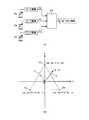
図5(a)は、入力装置1に対する入力操作の押圧方向および押圧強度を検出するための回路を示した図であり、同図(b)は、押圧方向を算出するための原理を示した図である。同図(a)に示すような回路を構成し、静電容量Ca、Cb、Ccに対して周期的に変化する電圧を加えると、各々の静電容量Ca、Cb、Ccに応じた電圧Va、Vb、Vcが得られる。これらの電圧Va、Vb、Vcは、入力装置1が入力操作を受けていない場合、すなわち待機状態では略同一の値となる。 FIG. 5A is a diagram showing a circuit for detecting the pressing direction and the pressing strength of the input operation on the
入力装置1が入力操作を受けると、押圧方向と押圧強度に応じて静電容量Ca、Cb、Ccがそれぞれ変化し、これに伴って待機状態の電圧Va、Vb、Vcに対する電圧の変化量dVa、dVb、dVcが得られる。得られた電圧変化量dVa、dVb、dVcは演算処理装置50に送信され、演算処理装置50は、受信した電圧変化量dVa、dVb、dVcに基づいて入力操作の押圧方向と押圧強度を算出する。すなわち、本実施形態では、演算処理装置50が押圧方向検出装置であり、且つ押圧強度検出装置となっている。 When the
押圧方向の算出は、本実施形態では、静電容量Ca、Cb、Ccの変化量、すなわち電圧変化量dVa、dVb、dVcの重心位置を求めることによって行う。具体的には、静電容量検出部32および可動電極20の中心Oを原点とする静電容量Ca、Cb、Ccのx−y座標をそれぞれ(xa,ya)、(xb,yb)、(xc,yc)とした場合に、X=(dVa・xa+dVb・xb+dVc・xc)/(dVa+dVb+dVc)、およびY=(dVa・ya+dVb・yb+dVc・yc)/(dVa+dVb+dVc)を算出する。そして、座標(X,Y)で表されるベクトルVを、押圧方向を示す量として求める。 In this embodiment, the pressing direction is calculated by obtaining the change amounts of the electrostatic capacitances Ca, Cb, and Cc, that is, the barycentric positions of the voltage change amounts dVa, dVb, and dVc. Specifically, the xy coordinates of the capacitances Ca, Cb, and Cc with the origin O at the center O of the
なお、本実施形態では、静電容量Ca、Cb、Ccは、中心Oを重心とする正三角形Tの各頂点に位置しているため、静電容量Ca、Cb、Ccの座標は、それぞれ(√3t,−t)、(0,2t)、(−√3t,−t)となっている。従って、上記X、Yを求める式は、X=kx(dVa−dVb)、Y=ky(2dVb−dVa−dVc)という形に簡略化することができる。ここで、係数kx、kyは、実際にはkx=t/(dVa+dVb+dVc)、ky=√3t/(dVa+dVb+dVc)であるが、信号状態に応じて適宜に補正して用いるようにすることができる。 In the present embodiment, the capacitances Ca, Cb, and Cc are located at the vertices of the equilateral triangle T with the center O as the center of gravity, so the coordinates of the capacitances Ca, Cb, and Cc are ( √3t, −t), (0, 2t), (−√3t, −t). Therefore, the equations for obtaining X and Y can be simplified to X = kx (dVa−dVb) and Y = ky (2dVb−dVa−dVc). Here, the coefficients kx and ky are actually kx = t / (dVa + dVb + dVc) and ky = √3t / (dVa + dVb + dVc), but can be appropriately corrected according to the signal state.
また、押圧強度の算出は、本実施形態では、電圧変化量dVa、dVb、dVcの総和S=dVa+dVb+dVcを押圧強度示す量として求める。算出したX、Y、およびSの値は、ホスト機器に送信される。 Further, in the present embodiment, the calculation of the pressing strength is obtained as an amount indicating the pressing strength by summing up the voltage change amounts dVa, dVb, dVc S = dVa + dVb + dVc. The calculated values of X, Y, and S are transmitted to the host device.
なお、演算処理装置50(押圧方向検出装置および押圧強度検出装置)は、入力装置1専用の装置として設けるようにしてもよいし、例えばホスト機器が備えるCPU(中央演算処理装置)の機能の一部として実現するようにしてもよい。また、演算処理装置50を入力装置1専用の装置として設ける場合、薄膜樹脂フィルム基板10上に演算処理装置50を実装するようにしてもよいし、薄膜樹脂フィルム基板10とは別に演算処理装置50を設けるようにしてもよい。 Note that the arithmetic processing device 50 (pressing direction detection device and pressing strength detection device) may be provided as a device dedicated to the
次に薄膜樹脂フィルム基板のその他の形態の例について説明する。 Next, examples of other forms of the thin film resin film substrate will be described.
図6は、静電容量検出電極32a、32b、32cを薄膜樹脂フィルム基板10の上面に形成した例を示した断面図である。同図に示されるように、静電容量検出電極32a、32b、32cを上面、すなわち可動電極20が固定される面に形成するようにしてもよい。この場合、可動電極20との電気的短絡を防止するために、絶縁層38が静電容量検出電極32a、32b、32c上に設けられる。この絶縁層38は、例えばポリイミドやPET等の絶縁基材および絶縁粘着材からなる樹脂テープから構成することができる。なお、さらに引出配線部34を、薄膜樹脂フィルム基板10の上面に形成するようにしてもよい。 FIG. 6 is a cross-sectional view showing an example in which the
次に、可動電極20のその他の形態の例について説明する。 Next, examples of other forms of the
図7(a)および(b)は、可動電極20の変移部22に静電容量検出用突起部22a、22b、22cを設けないようにした例を示した図である。なお、同図(a)は、入力装置1が入力操作を受けていない状態の断面を示しており、同図(b)は、入力装置1が入力操作を受けた状態の断面を示している。 FIGS. 7A and 7B are diagrams showing an example in which the
静電容量検出用突起部22a、22b、22cの形状は、特に限定されるものではなく、要求される操作感や静電容量Ca、Cb、Ccの変化量等に応じて、適宜の形状に設定することができ、この例に示すように、静電容量検出用突起部22a、22b、22cを全く設けないようにしてもよい。 The shape of the
図8(a)〜(c)は、可動電極20の変移部22に補助固定部26を設けた例を示した図である。なお、同図(a)は、この例の入力装置1の平面図である。また、同図(b)は、入力装置1が入力操作を受けていない状態の断面を示しており、同図(c)は、入力装置1が入力操作を受けた状態の断面を示している。 8A to 8C are diagrams showing an example in which the
この例では、変移部20の静電容量検出用突起部22a、22b、22cの間に3つの補助固定部26を設けている。これらの補助固定部26は、静電容量検出電極32a、32b、32cと対向しない位置において先端が薄膜樹脂フィルム基板10に当接するように構成されている。そして、補助固定部26の先端は、固定部24と同様に接着剤により薄膜樹脂フィルム基板10に接着される。 In this example, three
このように、固定部24の内側に補助固定部26を設けることにより、入力操作を受けていない状態での変移部22の形状を適切な状態に保つことができる。すなわち、静電容量検出電極32a、32b、32cとの距離を適切に保ち、待機状態における静電容量Ca、Cb、Ccが変化しないようにすることができる。また、補助固定部26を適宜の位置に設けることで入力操作を受けた場合の変移部22の変形量を調整することも可能であり、これにより、静電容量Ca、Cb、Ccの変化量を調節することもできる。 Thus, by providing the
なお、補助固定部26は、先端を薄膜樹脂フィルム10に接着するのではなく、先端を薄膜樹脂フィルム10の固定電極30以外の領域に当接させるだけであってもよい。 The
図9(a)〜(c)は、変移部22の中央に補助固定部26を設けると共に、静電容量検出用突起部22a、22b、22cの先端と対向する静電容量検出電極32a、32b、32cとの距離が外周側に向けて順次大きくなるように構成した例を示した図である。なお、同図(a)は、この例の入力装置1の平面図である。また、同図(b)は、入力装置1が入力操作を受けていない状態の断面を示しており、同図(c)は、入力装置1が入力操作を受けた状態の断面を示している。 9A to 9C, the
この例では、静電容量検出用突起部22a、22b、22cをサイズの異なる2つの略半球状の突起から構成し、外周側の突起の突出量を内周側の突起よりも少なくしている。このように、静電容量検出用突起部22a、22b、22cを、外周側に向けて徐々に薄膜樹脂フィルム基板10から離れるように構成することにより、操作感を硬くすることなく、静電容量Ca、Cb、Ccの変化量を大きくすることができる。すなわち、柔らかい良好な操作感と静電容量Ca、Cb、Ccの大きな変化量とを両立させることができる。 In this example, the
なお、この場合における静電容量検出用突起部22a、22b、22cの形状は、特に限定されるものではなく、例えば楔形状や階段状に静電容量検出用突起部22a、22b、22cを構成するようにしてもよい。また、補助固定部26は、必要に応じて省略するようにしてもよい。 In this case, the shape of the
図10(a)〜(c)は、変移部22を梁状の接続部材28を介して固定部24に支持されるようにした例を示した図である。なお、同図(a)は、この例の入力装置1の平面図である。また、同図(b)は、入力装置1が入力操作を受けていない状態の断面を示しており、同図(c)は、入力装置1が入力操作を受けた状態の断面を示している。 FIGS. 10A to 10C are diagrams showing an example in which the
この例では、円盤状の変移部22を、外周側の固定部24から梁状の接続部材28を介して支持することにより、変移部22の変移の自由度を高めるようにしている。このようにすることで、例えばステンレス等の金属から可動電極20を構成した場合にも、接続部材28の変形により柔らかい操作感が得られるようにすることができる。従って、入力装置1の耐久性と良好な操作感とを両立させることができる。 In this example, the disc-shaped
図11は、接続部材28のその他の形状の例を示した平面図である。接続部材28は、同図に示されるような形状に構成されるものであってもよい。なお、接続部材28の形状は、変移部22と固定部24を接続する梁状であればよく、特に限定されるものではないが、変移部22をスムーズに変移させ、良好な操作感を得るためには、変移部22に繋がる端部と固定部24に繋がる端部の位置を幅方向にずらすことが好ましい。 FIG. 11 is a plan view showing an example of another shape of the
以上説明したように、本実施形態に係る入力装置1は、固定電極30を形成した薄膜樹脂フィルム基板10と、導電性材料からなる可動電極20とを備え、固定電極30は、静電容量検出部32と、接続部36とを有し、可動電極20は、静電容量検出部32に対向配置されると共に押圧により変形する変移部22と、固定電極30の接続部36に接続した固定部24とを有し、静電容量検出部32は、3箇所の静電容量変化量に基づく押圧方向検出用として、同一直線上に並ばないように配置した3つの静電容量検出電極32a、32b、32cを有している。 As described above, the
このような構成とすることで、静電容量型の分野において抜本的に薄くできるばかりでなく、それと同時に材料ならびに製造コストを低減することができる。特に、従来4つ以上が常識であったx−yの2次元方向の押圧方向検出用の静電容量検出電極を3つに減らすことで、部品点数を削減し、入力装置1を薄くコンパクトに構成すると共に、製造コストを低減することができる。 By adopting such a configuration, not only can the thickness be drastically reduced in the field of capacitance type, but also material and manufacturing cost can be reduced at the same time. In particular, by reducing the number of electrostatic capacity detection electrodes for detecting the pressing direction in the two-dimensional direction of xy, which has been common knowledge of four or more, to three, the number of parts can be reduced and the
また、入力装置1は、3つの静電容量検出電極32a、32b、32cにおける静電容量変化量の重心位置を算出することによって押圧方向を検出する押圧方向検出装置(演算処理装置50)をさらに有している。このような構成とすることで、3つの静電容量検出電極32a、32b、32cのみから押圧方向を検出することが可能となる。結果として、部品点数を削減し、入力装置1を薄くコンパクトに構成すると共に、製造コストを低減することが可能となる。 Further, the
また、薄膜樹脂フィルム基板10は、可動電極20が配置された面とは反対側の面に静電容量検出電極32a、32b、32cが形成されており、変移部22が変形した場合に可動電極20と静電容量検出電極32a、32b、32cとの電気的短絡を防止する絶縁層として機能している。このような構成とすることで、新たな絶縁層を設ける必要がなく、入力装置1をさらに薄くコンパクトにすることができる。 The thin film
また、3つの静電容量検出電極32a、32b、32cは、押圧強度検出用として兼用されている。このような構成とすることで、押圧強度検出用の静電容量検出電極を省略することが可能となり、入力装置1をさらに薄くコンパクトに構成すると共に、製造コストを低減することができる。 The three
また、入力装置1は、3つの静電容量検出電極32a、32b、32cにおける静電容量変化量の総和を算出することによって押圧強度を検出する押圧強度検出装置(演算処理装置50)をさらに有している。このような構成とすることで、3つの静電容量検出電極32a、32b、32cのみから押圧強度を検出することが可能となる。結果として、入力装置1を薄くコンパクトに構成すると共に、製造コストを低減することが可能となる。 In addition, the
また、3つの静電容量検出電極32a、32b、32cは、静電容量検出部32の中心Oを重心とする正三角形Tの頂点位置に配置されている。このような構成とすることで、3つの静電容量検出電極32a、32b、32cにおける静電容量変化量を略均等にバランスさせることが可能となり、押圧方向および押圧強度の検出精度を向上させることができる。また、重心位置を算出する式を簡略化することができるため、処理速度を向上させることができる
また、入力装置1において、固定部24は、変移部22の外周に設けられ、変移部22は、静電容量検出電極32a、32b、32cと対向しない位置において薄膜樹脂フィルム基板10と当接する柱状の補助固定部26を有するように構成してもよい。このような構成とすることで、待機時および操作時における変移部22の形状を適正に保つことが可能となり、入力装置1の検出感度および検出精度を向上させることができる。The three
また、入力装置1において、補助固定部26は、変移部22の中央に設けられ、変移部22は、静電容量検出電極32a、32b、32cに向けて突出する複数の突起部(静電容量検出用突起部22a、22b、22c)を有し、複数の突起部22a、22b、22cの先端と対向する静電容量検出電極32a、32b、32cとの距離が外周側に向けて順次大きくなっているように構成してもよい。このような構成とすることで、入力装置1の良好な操作感および検出感度を最適化することができる。 Further, in the
また、入力装置1において、変移部22は、梁状の接続部材28を介して固定部24に支持されるように構成してもよい。このような構成とすることで、入力装置1の耐久性および良好な操作感を最適化することができる。 Further, in the
なお、本実施形態では、静電容量検出電極32a、32b、32cを、静電容量検出部32および可動電極20の中心Oを重心とする正三角形Tの各頂点に配置しているが、本発明はこれに限定されるものではなく、静電容量検出電極32a、32b、32cの配置は、同一直線状に配置しない限り、どのように配置であってもよい。すなわち、3箇所の静電容量変化量の重心位置の2次元座標を算出することが可能な配置であればよい。 In the present embodiment, the
従って、本発明によれば、例えば他の部品等と干渉しないように、ある程度任意に静電容量検出電極32a、32b、32cの配置を変更することができるため、各種ホスト機器への組み込みの自由度を向上させることが可能となっている。 Therefore, according to the present invention, for example, the arrangement of the
以上、本発明の実施の形態について説明したが、本発明の入力装置は、上記した実施の形態に限定されるものではなく、本発明の要旨を逸脱しない範囲内において種々変更を加え得ることは勿論である。 Although the embodiment of the present invention has been described above, the input device of the present invention is not limited to the above-described embodiment, and various modifications can be made without departing from the scope of the present invention. Of course.
本発明の入力装置は、入力操作を必要とする各種装置や電子機器において利用することができる。 The input device of the present invention can be used in various devices and electronic devices that require an input operation.
1 入力装置
10 薄膜樹脂フィルム基板
20 可動電極
22 変移部
22a、22b、22c 静電容量検出用突起部
24 固定部
26 補助固定部
28 接続部材
30 固定電極
32 静電容量検出部
32a、32b、32c 静電容量検出電極
36 接続部
50 演算処理装置
O 静電容量検出部および可動電極の中心DESCRIPTION OF
Claims (8)
Translated fromJapanese前記固定電極は、静電容量検出部と、接続部とを有し、
前記可動電極は、前記静電容量検出部に対向配置されると共に押圧により変形する変移部と、前記固定電極の接続部に接続した固定部とを有し、
前記静電容量検出部は、3箇所の静電容量変化量に基づく押圧方向検出用として、同一直線上に並ばないように配置した3つの静電容量検出電極を有し、
前記押圧方向検出装置は、前記3つの静電容量検出電極における静電容量変化量および前記3つの静電容量検出電極の位置から重心位置を算出することによって押圧方向を検出することを特徴とする、
入力装置。A thin film resin film substrate on which a fixed electrode is formed, a movable electrode made of a conductive material, anda pressing direction detection device that detects a pressing direction in an input operation ,
The fixed electrode has a capacitance detection unit and a connection unit,
The movable electrode has a transition portion that is disposed opposite to the capacitance detection portion and deforms when pressed, and a fixed portion connected to a connection portion of the fixed electrode,
The electrostatic capacitance detection unit, for the pressing direction detection based on the variation amount of capacitance of three,and have a three electrostatic capacitance detection electrodes arranged so as not aligned on the same straightline,
The pressing direction detecting device detects a pressing direction by calculating a center of gravity position from a capacitance change amount in the three capacitance detection electrodes and a position of the three capacitance detection electrodes. ,
Input device.
請求項1に記載の入力装置。The thin film resin film substrate has the capacitance detection electrode formed on a surface opposite to the surface on which the movable electrode is disposed, and the movable electrode and the capacitance when the transition portion is deformed. It functions as an insulating layer that prevents an electrical short circuit with the detection electrode,
The input device according to claim1 .
請求項1または2に記載の入力装置。The three capacitance detection electrodes are also used for pressure intensity detection,
The input device according to claim 1or 2 .
請求項1または2に記載の入力装置。It further has a pressure intensity detection device that detects the pressure intensity by calculating the sum of the capacitance change amounts in the three capacitance detection electrodes.
The input device according to claim 1or 2 .
請求項1乃至4のいずれかに記載の入力装置。The three capacitance detection electrodes are arranged at apexes of an equilateral triangle having the center of gravity of the capacitance detection unit as a center of gravity,
Input device according to any one of claims 1 to4.
前記変移部は、前記静電容量検出電極と対向しない位置において前記薄膜樹脂フィルム基板と当接する柱状の補助固定部を有することを特徴とする、
請求項1乃至5のいずれかに記載の入力装置。The fixing part is provided on the outer periphery of the transition part,
The transition part has a columnar auxiliary fixing part that comes into contact with the thin film resin film substrate at a position not facing the capacitance detection electrode.
Input device according to any one of claims 1 to5.
前記変移部は、前記静電容量検出電極に向けて突出する複数の突起部を有し、
前記複数の突起部の先端と対向する前記静電容量検出電極との距離が外周側に向けて順次大きくなっていることを特徴とする、
請求項6に記載の入力装置。The auxiliary fixing part is provided at the center of the transition part,
The transition part has a plurality of protrusions protruding toward the capacitance detection electrode,
The distance between the capacitance detection electrodes facing the tips of the plurality of protrusions is gradually increased toward the outer peripheral side,
The input device according to claim6 .
請求項1乃至7のいずれかに記載の入力装置。The transition part is supported by the fixed part via a beam-shaped connecting member,
Input device according toany one of claims 1 to7.
Priority Applications (1)
| Application Number | Priority Date | Filing Date | Title |
|---|---|---|---|
| JP2010046254AJP4756097B1 (en) | 2010-03-03 | 2010-03-03 | Input device |
Applications Claiming Priority (1)
| Application Number | Priority Date | Filing Date | Title |
|---|---|---|---|
| JP2010046254AJP4756097B1 (en) | 2010-03-03 | 2010-03-03 | Input device |
Publications (2)
| Publication Number | Publication Date |
|---|---|
| JP4756097B1true JP4756097B1 (en) | 2011-08-24 |
| JP2011180950A JP2011180950A (en) | 2011-09-15 |
Family
ID=44597142
Family Applications (1)
| Application Number | Title | Priority Date | Filing Date |
|---|---|---|---|
| JP2010046254AActiveJP4756097B1 (en) | 2010-03-03 | 2010-03-03 | Input device |
Country Status (1)
| Country | Link |
|---|---|
| JP (1) | JP4756097B1 (en) |
Cited By (1)
| Publication number | Priority date | Publication date | Assignee | Title |
|---|---|---|---|---|
| WO2020230853A1 (en) | 2019-05-16 | 2020-11-19 | Cyberdyne株式会社 | Tactile force detection device, tactile force detection method, and robot arm |
Families Citing this family (4)
| Publication number | Priority date | Publication date | Assignee | Title |
|---|---|---|---|---|
| JP2014142193A (en)* | 2013-01-22 | 2014-08-07 | Oga Inc | Load distribution detector |
| JP5962597B2 (en) | 2013-06-20 | 2016-08-03 | 株式会社デンソー | Operating device |
| WO2021184209A1 (en)* | 2020-03-17 | 2021-09-23 | 京东方科技集团股份有限公司 | Touch control positioning method and apparatus |
| WO2023181911A1 (en)* | 2022-03-24 | 2023-09-28 | パナソニックIpマネジメント株式会社 | Load sensor |
Family Cites Families (5)
| Publication number | Priority date | Publication date | Assignee | Title |
|---|---|---|---|---|
| JPH11111120A (en)* | 1997-09-30 | 1999-04-23 | Kokusai Electric Co Ltd | Key structure of small portable electronic devices |
| JPH11161420A (en)* | 1997-12-01 | 1999-06-18 | Alps Electric Co Ltd | Joy stick |
| JP4153266B2 (en)* | 2002-09-02 | 2008-09-24 | ポリマテック株式会社 | Analog switch output value correction method, computer program, and analog switch |
| JP4355553B2 (en)* | 2003-10-14 | 2009-11-04 | 修司 北澤 | Input key switch |
| JP2006331326A (en)* | 2005-05-30 | 2006-12-07 | Star Micronics Co Ltd | Pointing device |
- 2010
- 2010-03-03JPJP2010046254Apatent/JP4756097B1/enactiveActive
Cited By (2)
| Publication number | Priority date | Publication date | Assignee | Title |
|---|---|---|---|---|
| WO2020230853A1 (en) | 2019-05-16 | 2020-11-19 | Cyberdyne株式会社 | Tactile force detection device, tactile force detection method, and robot arm |
| US12123791B2 (en) | 2019-05-16 | 2024-10-22 | Cyberdyne Inc. | Haptic detection apparatus, haptic detection method, and robot arm |
Also Published As
| Publication number | Publication date |
|---|---|
| JP2011180950A (en) | 2011-09-15 |
Similar Documents
| Publication | Publication Date | Title |
|---|---|---|
| CN102132228B (en) | input device | |
| JP6032371B2 (en) | Detection sensor and input device | |
| KR102358388B1 (en) | Capacitive sensor for detecting touch position and pressing force | |
| US7372281B2 (en) | Capacitance type sensor | |
| US7499025B2 (en) | Pressing direction sensor and input device using the same | |
| WO2011096093A1 (en) | Input device | |
| US8079272B2 (en) | Tactile sensor | |
| JP4756097B1 (en) | Input device | |
| JP4996771B2 (en) | Electronic devices | |
| JP2004191348A (en) | Electrostatic capacity sensor and its manufacturing method | |
| JP2004045173A (en) | Capacitance type sensor | |
| US7710126B2 (en) | Capacitance type sensor | |
| US7705612B2 (en) | Capacitance type sensor | |
| JP6421329B2 (en) | Operation switch | |
| JP4226643B2 (en) | Straining body, capacitive force sensor and capacitive acceleration sensor | |
| JP6443989B2 (en) | Input device | |
| JP2002107245A (en) | Force detector | |
| WO2013024736A1 (en) | Force detector | |
| JP4392641B2 (en) | Force detection device | |
| JP2019074425A (en) | Detector and input device | |
| JP3842016B2 (en) | Input device | |
| KR101865304B1 (en) | Touch input device | |
| WO2019092953A1 (en) | Input device | |
| JP2012221012A (en) | Input device | |
| JP2011138674A (en) | Resistance sheet, pressure-sensitive switch, and input device using the same |
Legal Events
| Date | Code | Title | Description |
|---|---|---|---|
| A521 | Request for written amendment filed | Free format text:JAPANESE INTERMEDIATE CODE: A523 Effective date:20110415 | |
| TRDD | Decision of grant or rejection written | ||
| A01 | Written decision to grant a patent or to grant a registration (utility model) | Free format text:JAPANESE INTERMEDIATE CODE: A01 Effective date:20110517 | |
| A01 | Written decision to grant a patent or to grant a registration (utility model) | Free format text:JAPANESE INTERMEDIATE CODE: A01 | |
| A61 | First payment of annual fees (during grant procedure) | Free format text:JAPANESE INTERMEDIATE CODE: A61 Effective date:20110530 | |
| FPAY | Renewal fee payment (event date is renewal date of database) | Free format text:PAYMENT UNTIL: 20140603 Year of fee payment:3 | |
| R150 | Certificate of patent or registration of utility model | Ref document number:4756097 Country of ref document:JP Free format text:JAPANESE INTERMEDIATE CODE: R150 Free format text:JAPANESE INTERMEDIATE CODE: R150 | |
| R250 | Receipt of annual fees | Free format text:JAPANESE INTERMEDIATE CODE: R250 | |
| R250 | Receipt of annual fees | Free format text:JAPANESE INTERMEDIATE CODE: R250 | |
| S531 | Written request for registration of change of domicile | Free format text:JAPANESE INTERMEDIATE CODE: R313531 | |
| R350 | Written notification of registration of transfer | Free format text:JAPANESE INTERMEDIATE CODE: R350 | |
| R250 | Receipt of annual fees | Free format text:JAPANESE INTERMEDIATE CODE: R250 | |
| R250 | Receipt of annual fees | Free format text:JAPANESE INTERMEDIATE CODE: R250 | |
| R250 | Receipt of annual fees | Free format text:JAPANESE INTERMEDIATE CODE: R250 | |
| R250 | Receipt of annual fees | Free format text:JAPANESE INTERMEDIATE CODE: R250 |