JP4753904B2 - Light emitting device - Google Patents
Light emitting deviceDownload PDFInfo
- Publication number
- JP4753904B2 JP4753904B2JP2007067362AJP2007067362AJP4753904B2JP 4753904 B2JP4753904 B2JP 4753904B2JP 2007067362 AJP2007067362 AJP 2007067362AJP 2007067362 AJP2007067362 AJP 2007067362AJP 4753904 B2JP4753904 B2JP 4753904B2
- Authority
- JP
- Japan
- Prior art keywords
- light emitting
- emitting device
- light
- sealing body
- wiring pattern
- Prior art date
- Legal status (The legal status is an assumption and is not a legal conclusion. Google has not performed a legal analysis and makes no representation as to the accuracy of the status listed.)
- Expired - Fee Related
Links
Images


Classifications
- H—ELECTRICITY
- H10—SEMICONDUCTOR DEVICES; ELECTRIC SOLID-STATE DEVICES NOT OTHERWISE PROVIDED FOR
- H10H—INORGANIC LIGHT-EMITTING SEMICONDUCTOR DEVICES HAVING POTENTIAL BARRIERS
- H10H20/00—Individual inorganic light-emitting semiconductor devices having potential barriers, e.g. light-emitting diodes [LED]
- H10H20/80—Constructional details
- H10H20/85—Packages
- H10H20/851—Wavelength conversion means
- H10H20/8511—Wavelength conversion means characterised by their material, e.g. binder
- H10H20/8512—Wavelength conversion materials
- F—MECHANICAL ENGINEERING; LIGHTING; HEATING; WEAPONS; BLASTING
- F21—LIGHTING
- F21K—NON-ELECTRIC LIGHT SOURCES USING LUMINESCENCE; LIGHT SOURCES USING ELECTROCHEMILUMINESCENCE; LIGHT SOURCES USING CHARGES OF COMBUSTIBLE MATERIAL; LIGHT SOURCES USING SEMICONDUCTOR DEVICES AS LIGHT-GENERATING ELEMENTS; LIGHT SOURCES NOT OTHERWISE PROVIDED FOR
- F21K9/00—Light sources using semiconductor devices as light-generating elements, e.g. using light-emitting diodes [LED] or lasers
- F21K9/20—Light sources comprising attachment means
- F—MECHANICAL ENGINEERING; LIGHTING; HEATING; WEAPONS; BLASTING
- F21—LIGHTING
- F21V—FUNCTIONAL FEATURES OR DETAILS OF LIGHTING DEVICES OR SYSTEMS THEREOF; STRUCTURAL COMBINATIONS OF LIGHTING DEVICES WITH OTHER ARTICLES, NOT OTHERWISE PROVIDED FOR
- F21V23/00—Arrangement of electric circuit elements in or on lighting devices
- F21V23/001—Arrangement of electric circuit elements in or on lighting devices the elements being electrical wires or cables
- F21V23/002—Arrangements of cables or conductors inside a lighting device, e.g. means for guiding along parts of the housing or in a pivoting arm
- H—ELECTRICITY
- H01—ELECTRIC ELEMENTS
- H01L—SEMICONDUCTOR DEVICES NOT COVERED BY CLASS H10
- H01L25/00—Assemblies consisting of a plurality of semiconductor or other solid state devices
- H01L25/03—Assemblies consisting of a plurality of semiconductor or other solid state devices all the devices being of a type provided for in a single subclass of subclasses H10B, H10D, H10F, H10H, H10K or H10N, e.g. assemblies of rectifier diodes
- H01L25/04—Assemblies consisting of a plurality of semiconductor or other solid state devices all the devices being of a type provided for in a single subclass of subclasses H10B, H10D, H10F, H10H, H10K or H10N, e.g. assemblies of rectifier diodes the devices not having separate containers
- H01L25/075—Assemblies consisting of a plurality of semiconductor or other solid state devices all the devices being of a type provided for in a single subclass of subclasses H10B, H10D, H10F, H10H, H10K or H10N, e.g. assemblies of rectifier diodes the devices not having separate containers the devices being of a type provided for in group H10H20/00
- H01L25/0753—Assemblies consisting of a plurality of semiconductor or other solid state devices all the devices being of a type provided for in a single subclass of subclasses H10B, H10D, H10F, H10H, H10K or H10N, e.g. assemblies of rectifier diodes the devices not having separate containers the devices being of a type provided for in group H10H20/00 the devices being arranged next to each other
- H—ELECTRICITY
- H10—SEMICONDUCTOR DEVICES; ELECTRIC SOLID-STATE DEVICES NOT OTHERWISE PROVIDED FOR
- H10H—INORGANIC LIGHT-EMITTING SEMICONDUCTOR DEVICES HAVING POTENTIAL BARRIERS
- H10H20/00—Individual inorganic light-emitting semiconductor devices having potential barriers, e.g. light-emitting diodes [LED]
- H10H20/80—Constructional details
- H10H20/81—Bodies
- H10H20/822—Materials of the light-emitting regions
- H10H20/824—Materials of the light-emitting regions comprising only Group III-V materials, e.g. GaP
- H10H20/825—Materials of the light-emitting regions comprising only Group III-V materials, e.g. GaP containing nitrogen, e.g. GaN
- H—ELECTRICITY
- H10—SEMICONDUCTOR DEVICES; ELECTRIC SOLID-STATE DEVICES NOT OTHERWISE PROVIDED FOR
- H10H—INORGANIC LIGHT-EMITTING SEMICONDUCTOR DEVICES HAVING POTENTIAL BARRIERS
- H10H20/00—Individual inorganic light-emitting semiconductor devices having potential barriers, e.g. light-emitting diodes [LED]
- H10H20/80—Constructional details
- H10H20/83—Electrodes
- H10H20/831—Electrodes characterised by their shape
- H—ELECTRICITY
- H10—SEMICONDUCTOR DEVICES; ELECTRIC SOLID-STATE DEVICES NOT OTHERWISE PROVIDED FOR
- H10H—INORGANIC LIGHT-EMITTING SEMICONDUCTOR DEVICES HAVING POTENTIAL BARRIERS
- H10H20/00—Individual inorganic light-emitting semiconductor devices having potential barriers, e.g. light-emitting diodes [LED]
- H10H20/80—Constructional details
- H10H20/85—Packages
- H10H20/852—Encapsulations
- H10H20/854—Encapsulations characterised by their material, e.g. epoxy or silicone resins
- H—ELECTRICITY
- H10—SEMICONDUCTOR DEVICES; ELECTRIC SOLID-STATE DEVICES NOT OTHERWISE PROVIDED FOR
- H10H—INORGANIC LIGHT-EMITTING SEMICONDUCTOR DEVICES HAVING POTENTIAL BARRIERS
- H10H20/00—Individual inorganic light-emitting semiconductor devices having potential barriers, e.g. light-emitting diodes [LED]
- H10H20/80—Constructional details
- H10H20/85—Packages
- H10H20/855—Optical field-shaping means, e.g. lenses
- H10H20/856—Reflecting means
- H—ELECTRICITY
- H10—SEMICONDUCTOR DEVICES; ELECTRIC SOLID-STATE DEVICES NOT OTHERWISE PROVIDED FOR
- H10H—INORGANIC LIGHT-EMITTING SEMICONDUCTOR DEVICES HAVING POTENTIAL BARRIERS
- H10H20/00—Individual inorganic light-emitting semiconductor devices having potential barriers, e.g. light-emitting diodes [LED]
- H10H20/80—Constructional details
- H10H20/85—Packages
- H10H20/857—Interconnections, e.g. lead-frames, bond wires or solder balls
- H—ELECTRICITY
- H10—SEMICONDUCTOR DEVICES; ELECTRIC SOLID-STATE DEVICES NOT OTHERWISE PROVIDED FOR
- H10H—INORGANIC LIGHT-EMITTING SEMICONDUCTOR DEVICES HAVING POTENTIAL BARRIERS
- H10H20/00—Individual inorganic light-emitting semiconductor devices having potential barriers, e.g. light-emitting diodes [LED]
- H10H20/80—Constructional details
- H10H20/85—Packages
- H10H20/858—Means for heat extraction or cooling
- H10H20/8581—Means for heat extraction or cooling characterised by their material
- F—MECHANICAL ENGINEERING; LIGHTING; HEATING; WEAPONS; BLASTING
- F21—LIGHTING
- F21K—NON-ELECTRIC LIGHT SOURCES USING LUMINESCENCE; LIGHT SOURCES USING ELECTROCHEMILUMINESCENCE; LIGHT SOURCES USING CHARGES OF COMBUSTIBLE MATERIAL; LIGHT SOURCES USING SEMICONDUCTOR DEVICES AS LIGHT-GENERATING ELEMENTS; LIGHT SOURCES NOT OTHERWISE PROVIDED FOR
- F21K9/00—Light sources using semiconductor devices as light-generating elements, e.g. using light-emitting diodes [LED] or lasers
- F21K9/20—Light sources comprising attachment means
- F21K9/23—Retrofit light sources for lighting devices with a single fitting for each light source, e.g. for substitution of incandescent lamps with bayonet or threaded fittings
- F21K9/232—Retrofit light sources for lighting devices with a single fitting for each light source, e.g. for substitution of incandescent lamps with bayonet or threaded fittings specially adapted for generating an essentially omnidirectional light distribution, e.g. with a glass bulb
- F—MECHANICAL ENGINEERING; LIGHTING; HEATING; WEAPONS; BLASTING
- F21—LIGHTING
- F21Y—INDEXING SCHEME ASSOCIATED WITH SUBCLASSES F21K, F21L, F21S and F21V, RELATING TO THE FORM OR THE KIND OF THE LIGHT SOURCES OR OF THE COLOUR OF THE LIGHT EMITTED
- F21Y2105/00—Planar light sources
- F21Y2105/10—Planar light sources comprising a two-dimensional array of point-like light-generating elements
- F—MECHANICAL ENGINEERING; LIGHTING; HEATING; WEAPONS; BLASTING
- F21—LIGHTING
- F21Y—INDEXING SCHEME ASSOCIATED WITH SUBCLASSES F21K, F21L, F21S and F21V, RELATING TO THE FORM OR THE KIND OF THE LIGHT SOURCES OR OF THE COLOUR OF THE LIGHT EMITTED
- F21Y2115/00—Light-generating elements of semiconductor light sources
- F21Y2115/10—Light-emitting diodes [LED]
- H—ELECTRICITY
- H01—ELECTRIC ELEMENTS
- H01L—SEMICONDUCTOR DEVICES NOT COVERED BY CLASS H10
- H01L2224/00—Indexing scheme for arrangements for connecting or disconnecting semiconductor or solid-state bodies and methods related thereto as covered by H01L24/00
- H01L2224/01—Means for bonding being attached to, or being formed on, the surface to be connected, e.g. chip-to-package, die-attach, "first-level" interconnects; Manufacturing methods related thereto
- H01L2224/42—Wire connectors; Manufacturing methods related thereto
- H01L2224/44—Structure, shape, material or disposition of the wire connectors prior to the connecting process
- H01L2224/45—Structure, shape, material or disposition of the wire connectors prior to the connecting process of an individual wire connector
- H01L2224/45001—Core members of the connector
- H01L2224/45099—Material
- H01L2224/451—Material with a principal constituent of the material being a metal or a metalloid, e.g. boron (B), silicon (Si), germanium (Ge), arsenic (As), antimony (Sb), tellurium (Te) and polonium (Po), and alloys thereof
- H01L2224/45117—Material with a principal constituent of the material being a metal or a metalloid, e.g. boron (B), silicon (Si), germanium (Ge), arsenic (As), antimony (Sb), tellurium (Te) and polonium (Po), and alloys thereof the principal constituent melting at a temperature of greater than or equal to 400°C and less than 950°C
- H01L2224/45124—Aluminium (Al) as principal constituent
- H—ELECTRICITY
- H01—ELECTRIC ELEMENTS
- H01L—SEMICONDUCTOR DEVICES NOT COVERED BY CLASS H10
- H01L2224/00—Indexing scheme for arrangements for connecting or disconnecting semiconductor or solid-state bodies and methods related thereto as covered by H01L24/00
- H01L2224/01—Means for bonding being attached to, or being formed on, the surface to be connected, e.g. chip-to-package, die-attach, "first-level" interconnects; Manufacturing methods related thereto
- H01L2224/42—Wire connectors; Manufacturing methods related thereto
- H01L2224/44—Structure, shape, material or disposition of the wire connectors prior to the connecting process
- H01L2224/45—Structure, shape, material or disposition of the wire connectors prior to the connecting process of an individual wire connector
- H01L2224/45001—Core members of the connector
- H01L2224/45099—Material
- H01L2224/451—Material with a principal constituent of the material being a metal or a metalloid, e.g. boron (B), silicon (Si), germanium (Ge), arsenic (As), antimony (Sb), tellurium (Te) and polonium (Po), and alloys thereof
- H01L2224/45138—Material with a principal constituent of the material being a metal or a metalloid, e.g. boron (B), silicon (Si), germanium (Ge), arsenic (As), antimony (Sb), tellurium (Te) and polonium (Po), and alloys thereof the principal constituent melting at a temperature of greater than or equal to 950°C and less than 1550°C
- H01L2224/45144—Gold (Au) as principal constituent
- H—ELECTRICITY
- H01—ELECTRIC ELEMENTS
- H01L—SEMICONDUCTOR DEVICES NOT COVERED BY CLASS H10
- H01L2224/00—Indexing scheme for arrangements for connecting or disconnecting semiconductor or solid-state bodies and methods related thereto as covered by H01L24/00
- H01L2224/01—Means for bonding being attached to, or being formed on, the surface to be connected, e.g. chip-to-package, die-attach, "first-level" interconnects; Manufacturing methods related thereto
- H01L2224/42—Wire connectors; Manufacturing methods related thereto
- H01L2224/44—Structure, shape, material or disposition of the wire connectors prior to the connecting process
- H01L2224/45—Structure, shape, material or disposition of the wire connectors prior to the connecting process of an individual wire connector
- H01L2224/45001—Core members of the connector
- H01L2224/45099—Material
- H01L2224/451—Material with a principal constituent of the material being a metal or a metalloid, e.g. boron (B), silicon (Si), germanium (Ge), arsenic (As), antimony (Sb), tellurium (Te) and polonium (Po), and alloys thereof
- H01L2224/45138—Material with a principal constituent of the material being a metal or a metalloid, e.g. boron (B), silicon (Si), germanium (Ge), arsenic (As), antimony (Sb), tellurium (Te) and polonium (Po), and alloys thereof the principal constituent melting at a temperature of greater than or equal to 950°C and less than 1550°C
- H01L2224/45147—Copper (Cu) as principal constituent
- H—ELECTRICITY
- H01—ELECTRIC ELEMENTS
- H01L—SEMICONDUCTOR DEVICES NOT COVERED BY CLASS H10
- H01L2224/00—Indexing scheme for arrangements for connecting or disconnecting semiconductor or solid-state bodies and methods related thereto as covered by H01L24/00
- H01L2224/01—Means for bonding being attached to, or being formed on, the surface to be connected, e.g. chip-to-package, die-attach, "first-level" interconnects; Manufacturing methods related thereto
- H01L2224/42—Wire connectors; Manufacturing methods related thereto
- H01L2224/44—Structure, shape, material or disposition of the wire connectors prior to the connecting process
- H01L2224/45—Structure, shape, material or disposition of the wire connectors prior to the connecting process of an individual wire connector
- H01L2224/45001—Core members of the connector
- H01L2224/45099—Material
- H01L2224/451—Material with a principal constituent of the material being a metal or a metalloid, e.g. boron (B), silicon (Si), germanium (Ge), arsenic (As), antimony (Sb), tellurium (Te) and polonium (Po), and alloys thereof
- H01L2224/45163—Material with a principal constituent of the material being a metal or a metalloid, e.g. boron (B), silicon (Si), germanium (Ge), arsenic (As), antimony (Sb), tellurium (Te) and polonium (Po), and alloys thereof the principal constituent melting at a temperature of greater than 1550°C
- H01L2224/45169—Platinum (Pt) as principal constituent
- H—ELECTRICITY
- H01—ELECTRIC ELEMENTS
- H01L—SEMICONDUCTOR DEVICES NOT COVERED BY CLASS H10
- H01L2224/00—Indexing scheme for arrangements for connecting or disconnecting semiconductor or solid-state bodies and methods related thereto as covered by H01L24/00
- H01L2224/01—Means for bonding being attached to, or being formed on, the surface to be connected, e.g. chip-to-package, die-attach, "first-level" interconnects; Manufacturing methods related thereto
- H01L2224/42—Wire connectors; Manufacturing methods related thereto
- H01L2224/47—Structure, shape, material or disposition of the wire connectors after the connecting process
- H01L2224/48—Structure, shape, material or disposition of the wire connectors after the connecting process of an individual wire connector
- H01L2224/4805—Shape
- H01L2224/4809—Loop shape
- H01L2224/48091—Arched
- H—ELECTRICITY
- H01—ELECTRIC ELEMENTS
- H01L—SEMICONDUCTOR DEVICES NOT COVERED BY CLASS H10
- H01L2224/00—Indexing scheme for arrangements for connecting or disconnecting semiconductor or solid-state bodies and methods related thereto as covered by H01L24/00
- H01L2224/01—Means for bonding being attached to, or being formed on, the surface to be connected, e.g. chip-to-package, die-attach, "first-level" interconnects; Manufacturing methods related thereto
- H01L2224/42—Wire connectors; Manufacturing methods related thereto
- H01L2224/47—Structure, shape, material or disposition of the wire connectors after the connecting process
- H01L2224/48—Structure, shape, material or disposition of the wire connectors after the connecting process of an individual wire connector
- H01L2224/484—Connecting portions
- H01L2224/48463—Connecting portions the connecting portion on the bonding area of the semiconductor or solid-state body being a ball bond
- H01L2224/48465—Connecting portions the connecting portion on the bonding area of the semiconductor or solid-state body being a ball bond the other connecting portion not on the bonding area being a wedge bond, i.e. ball-to-wedge, regular stitch
- H—ELECTRICITY
- H01—ELECTRIC ELEMENTS
- H01L—SEMICONDUCTOR DEVICES NOT COVERED BY CLASS H10
- H01L2224/00—Indexing scheme for arrangements for connecting or disconnecting semiconductor or solid-state bodies and methods related thereto as covered by H01L24/00
- H01L2224/73—Means for bonding being of different types provided for in two or more of groups H01L2224/10, H01L2224/18, H01L2224/26, H01L2224/34, H01L2224/42, H01L2224/50, H01L2224/63, H01L2224/71
- H01L2224/732—Location after the connecting process
- H01L2224/73251—Location after the connecting process on different surfaces
- H01L2224/73265—Layer and wire connectors
- H—ELECTRICITY
- H01—ELECTRIC ELEMENTS
- H01L—SEMICONDUCTOR DEVICES NOT COVERED BY CLASS H10
- H01L24/00—Arrangements for connecting or disconnecting semiconductor or solid-state bodies; Methods or apparatus related thereto
- H01L24/01—Means for bonding being attached to, or being formed on, the surface to be connected, e.g. chip-to-package, die-attach, "first-level" interconnects; Manufacturing methods related thereto
- H01L24/42—Wire connectors; Manufacturing methods related thereto
- H01L24/44—Structure, shape, material or disposition of the wire connectors prior to the connecting process
- H01L24/45—Structure, shape, material or disposition of the wire connectors prior to the connecting process of an individual wire connector
- H—ELECTRICITY
- H01—ELECTRIC ELEMENTS
- H01L—SEMICONDUCTOR DEVICES NOT COVERED BY CLASS H10
- H01L2924/00—Indexing scheme for arrangements or methods for connecting or disconnecting semiconductor or solid-state bodies as covered by H01L24/00
- H01L2924/01—Chemical elements
- H01L2924/01015—Phosphorus [P]
- H—ELECTRICITY
- H01—ELECTRIC ELEMENTS
- H01L—SEMICONDUCTOR DEVICES NOT COVERED BY CLASS H10
- H01L2924/00—Indexing scheme for arrangements or methods for connecting or disconnecting semiconductor or solid-state bodies as covered by H01L24/00
- H01L2924/01—Chemical elements
- H01L2924/01047—Silver [Ag]
- H—ELECTRICITY
- H01—ELECTRIC ELEMENTS
- H01L—SEMICONDUCTOR DEVICES NOT COVERED BY CLASS H10
- H01L2924/00—Indexing scheme for arrangements or methods for connecting or disconnecting semiconductor or solid-state bodies as covered by H01L24/00
- H01L2924/01—Chemical elements
- H01L2924/01068—Erbium [Er]
- H—ELECTRICITY
- H01—ELECTRIC ELEMENTS
- H01L—SEMICONDUCTOR DEVICES NOT COVERED BY CLASS H10
- H01L2924/00—Indexing scheme for arrangements or methods for connecting or disconnecting semiconductor or solid-state bodies as covered by H01L24/00
- H01L2924/01—Chemical elements
- H01L2924/01087—Francium [Fr]
- H—ELECTRICITY
- H01—ELECTRIC ELEMENTS
- H01L—SEMICONDUCTOR DEVICES NOT COVERED BY CLASS H10
- H01L2924/00—Indexing scheme for arrangements or methods for connecting or disconnecting semiconductor or solid-state bodies as covered by H01L24/00
- H01L2924/095—Indexing scheme for arrangements or methods for connecting or disconnecting semiconductor or solid-state bodies as covered by H01L24/00 with a principal constituent of the material being a combination of two or more materials provided in the groups H01L2924/013 - H01L2924/0715
- H01L2924/097—Glass-ceramics, e.g. devitrified glass
- H01L2924/09701—Low temperature co-fired ceramic [LTCC]
- H—ELECTRICITY
- H01—ELECTRIC ELEMENTS
- H01L—SEMICONDUCTOR DEVICES NOT COVERED BY CLASS H10
- H01L2924/00—Indexing scheme for arrangements or methods for connecting or disconnecting semiconductor or solid-state bodies as covered by H01L24/00
- H01L2924/10—Details of semiconductor or other solid state devices to be connected
- H01L2924/11—Device type
- H01L2924/12—Passive devices, e.g. 2 terminal devices
- H01L2924/1204—Optical Diode
- H01L2924/12041—LED
- H—ELECTRICITY
- H01—ELECTRIC ELEMENTS
- H01L—SEMICONDUCTOR DEVICES NOT COVERED BY CLASS H10
- H01L2924/00—Indexing scheme for arrangements or methods for connecting or disconnecting semiconductor or solid-state bodies as covered by H01L24/00
- H01L2924/15—Details of package parts other than the semiconductor or other solid state devices to be connected
- H01L2924/181—Encapsulation
- H—ELECTRICITY
- H01—ELECTRIC ELEMENTS
- H01L—SEMICONDUCTOR DEVICES NOT COVERED BY CLASS H10
- H01L2924/00—Indexing scheme for arrangements or methods for connecting or disconnecting semiconductor or solid-state bodies as covered by H01L24/00
- H01L2924/30—Technical effects
- H01L2924/301—Electrical effects
- H01L2924/3011—Impedance
- H—ELECTRICITY
- H01—ELECTRIC ELEMENTS
- H01L—SEMICONDUCTOR DEVICES NOT COVERED BY CLASS H10
- H01L2924/00—Indexing scheme for arrangements or methods for connecting or disconnecting semiconductor or solid-state bodies as covered by H01L24/00
- H01L2924/30—Technical effects
- H01L2924/301—Electrical effects
- H01L2924/3025—Electromagnetic shielding
Landscapes
- Engineering & Computer Science (AREA)
- Microelectronics & Electronic Packaging (AREA)
- Physics & Mathematics (AREA)
- General Engineering & Computer Science (AREA)
- Power Engineering (AREA)
- Optics & Photonics (AREA)
- Condensed Matter Physics & Semiconductors (AREA)
- General Physics & Mathematics (AREA)
- Computer Hardware Design (AREA)
- Led Device Packages (AREA)
- Led Devices (AREA)
- Non-Portable Lighting Devices Or Systems Thereof (AREA)
Abstract
Description
Translated fromJapanese本発明は、発光装置およびその製造方法に関する。 The present invention relates to a light emitting device and a method for manufacturing the same.
近年、照明装置の光源としてLEDが多く用いられるようになってきている。LEDを使った照明装置の白色光を得る方法として、赤色LED、青色LEDおよび緑色LEDの三種類のLEDを用いる方法、青色LEDから発した励起光を変換して黄色光を発する蛍光体を用いる方法などがある。照明用光源としては、十分な輝度の白色光が要求されているために、LEDチップを複数個用いた照明装置が商品化されている。 In recent years, many LEDs have been used as light sources for lighting devices. As a method for obtaining white light of an illumination device using LEDs, a method using three types of LEDs, a red LED, a blue LED, and a green LED, and a phosphor that emits yellow light by converting excitation light emitted from the blue LED is used. There are methods. As a light source for illumination, white light with sufficient luminance is required, and lighting devices using a plurality of LED chips have been commercialized.
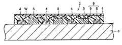
このような照明装置の一例として、たとえば特開2003−152225号公報(特許文献1)には、図14に模式的に示すような発光装置101が開示されている。図14に示す発光装置101は、アルミニウムで形成された金属板102上に凹状の素子格納部103が設けられるとともに、素子格納部間には、絶縁性のガラスエポキシ基板であって、その上に銅箔で形成された配線部105が設けられたプリント回路基板104が形成されてなる。そして、図14に示す例では、素子格納部103に載置(配置)された発光素子106と、前記プリント回路基板104上の配線部105とが、ボンディングワイヤ107を介して電気的に接続されてなる。さらに、この素子格納部103を、発光素子106およびボンディングワイヤ107ごと覆うようにして、樹脂封止体108にて封止されて構成される。特許文献1には、このような構成を備えることによって、放熱性を向上でき、かつ、発光ダイオードチップからの光を効率良く外部へ取り出すことができる発光装置を提供できると記載されている。As an example of such an illuminating device, for example, Japanese Patent Laying-Open No. 2003-152225 (Patent Document 1) discloses a
しかしながら、図14に示すような発光装置101では、アルミニウムで形成された金属板102の直近に、銅箔で形成された配線部105が設けられたプリント回路基板104が配置されている(図中、金属板102と配線部105との間の間隔として、水平方向に関する直線距離dを示している)。このため、金属板102と配線部105との間に充分な電気的絶縁が達成されていないことが想定される。また、図14に示すような発光装置101では、ガラスエポキシ基板で形成されたプリント回路基板104を有するため、製造工程が複雑となり、安価な発光装置を提供できないという問題もある。However, in the
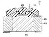
また、たとえば特開2006−287020号公報(特許文献2)には、図15に模式的に示すようなLED部品201が開示されている。図15に示すLED部品201は、配線基板202に形成された貫通孔内に、LEDチップ204が搭載された金属またはセラミックで形成された放熱板203が接合されてなる。そして、図15に示す例では、LEDチップ204と、配線基板202に形成された配線パターン205とがボンディングワイヤWにより電気的に接続され、このLEDチップ204およびボンディングワイヤW
が透明樹脂で形成された樹脂封止体206により埋設されてなる。特許文献2には、このような構成を備えることによって、LEDチップの発熱を効率的に放熱させることができ、生産性に優れた表面実装型のLED部品およびその製造方法を提供できると記載されている。Further, for example, Japanese Patent Laid-Open No. 2006-287020 (Patent Document 2) discloses an
Is embedded by a resin sealing
しかしながら、特許文献2には、LEDチップ204およびボンディングワイヤWを埋設するための透明樹脂を塗布する方法について詳細には記載されていない。また、特許文献2に開示された図15に示すLED部品201では、配線パターン205は配線基板202の側面と裏面の一部に形成されているため製造が困難であり、安価に製造することができないという問題がある。
本発明は、上記課題を解決するためになされたものであって、その目的とするところは、充分な電気的絶縁が達成でき、かつ、製造工程が容易で安価に製造することができる発光装置およびその製造方法を提供することである。 The present invention has been made in order to solve the above-described problems, and an object of the present invention is to provide a light emitting device that can achieve sufficient electrical insulation, can be easily manufactured at low cost. And a method of manufacturing the same.
本発明の発光装置は、絶縁基板上に、直線状の配線パターンが平行に配置されて複数形成され、その配線パターン間に複数個の発光素子が配線パターンに電気的に接続された状態で搭載され、封止体で封止された発光部を備えることを特徴とする。 The light emitting device of the present invention is mounted in a state where a plurality of linear wiring patterns are arranged in parallel on an insulating substrate, and a plurality of light emitting elements are electrically connected to the wiring patterns between the wiring patterns. And a light emitting portion sealed with a sealing body.
本発明の発光装置において、発光素子は、直線状の配線パターンを挟んで、直線状に配列されて複数個搭載されていることが好ましい。また、配線パターンを挟んで搭載された発光素子は、側面同士が対向しないようにずらして配置されていることがより好ましい。 In the light-emitting device of the present invention, it is preferable that a plurality of light-emitting elements are arranged in a straight line with a straight wiring pattern interposed therebetween. In addition, it is more preferable that the light emitting elements mounted with the wiring pattern interposed therebetween are arranged so that the side surfaces do not face each other.
また本発明の発光装置においては、断面形状が長方形状である発光素子が、その短辺に沿った方向が配線パターンの長手方向と平行になるように搭載されていることが好ましく、発光素子が長尺状の断面形状を有するものであることがより好ましい。 In the light-emitting device of the present invention, the light-emitting element having a rectangular cross-sectional shape is preferably mounted so that the direction along the short side is parallel to the longitudinal direction of the wiring pattern. It is more preferable that it has a long cross-sectional shape.
本発明の発光装置において、直線状の配線パターンを挟んで搭載された発光素子同士が直列に電気的に接続されていることが好ましい。また、直線状の配線パターンに沿って直線状に搭載された発光素子同士は、並列に電気的に接続されていることが、より好ましい。 In the light emitting device of the present invention, it is preferable that the light emitting elements mounted with the linear wiring pattern interposed therebetween are electrically connected in series. Moreover, it is more preferable that the light emitting elements mounted linearly along the linear wiring pattern are electrically connected in parallel.
本発明の発光装置における配線パターンは、発光素子との間の電気的接続の位置決め用のパターン、または、発光素子の搭載位置の目安用のパターンをさらに有することが好ましい。 The wiring pattern in the light emitting device of the present invention preferably further has a pattern for positioning electrical connection with the light emitting element or a pattern for indicating the mounting position of the light emitting element.
また本発明の発光装置は、発光素子と配線パターンとの間の直線距離が0.1mm以上であることが好ましい。 In the light emitting device of the present invention, the linear distance between the light emitting element and the wiring pattern is preferably 0.1 mm or more.
本発明の発光装置において、絶縁基板は白色のセラミック基板であることが好ましく、当該白色のセラミック基板は、酸化アルミニウム、窒化アルミニウム、ボロンナイトライド、窒化ケイ素、酸化マグネシウム、フォルステライト、ステアタイト、低温焼結セラミックから選ばれるいずれか、または、これらの複合材料で形成されていることがより好ましい。 In the light emitting device of the present invention, the insulating substrate is preferably a white ceramic substrate, and the white ceramic substrate is aluminum oxide, aluminum nitride, boron nitride, silicon nitride, magnesium oxide, forsterite, steatite, low temperature More preferably, it is formed of any one selected from sintered ceramics or a composite material thereof.
本発明の発光装置は、絶縁基板上の直線状の配線パターンおよび発光素子の全てが1つの封止体で封止されていることが好ましい。 In the light emitting device of the present invention, it is preferable that all of the linear wiring pattern and the light emitting element on the insulating substrate are sealed with one sealing body.
また本発明の発光装置は、封止体が蛍光体を含有することが好ましく、封止体が、第1の蛍光体を含有する第1の封止体層と、当該第1の封止体層上に積層された第2の蛍光体を含有する第2の封止体層とを備えることが、より好ましい。またこの場合、第2の封止体層が、第1の封止体層の少なくとも一部を覆うように第1の封止体層上に積層されていることが好ましい。 In the light-emitting device of the present invention, the sealing body preferably contains a phosphor, and the sealing body includes a first sealing body layer containing the first phosphor and the first sealing body. It is more preferable to include a second encapsulant layer containing a second phosphor laminated on the layer. In this case, it is preferable that the second sealing body layer is laminated on the first sealing body layer so as to cover at least a part of the first sealing body layer.
本発明の発光装置において、封止体は、六角形状、円形状、長方形状または正方形状の断面を有する形状に形成されていることが好ましい。 In the light emitting device of the present invention, the sealing body is preferably formed in a shape having a hexagonal shape, a circular shape, a rectangular shape, or a square-shaped cross section.
また本発明の発光装置は、円形状または正方形状の断面を有する形状であることが好ましい。 The light emitting device of the present invention preferably has a circular or square cross section.
本発明の発光装置は、液晶ディスプレイのバックライト光源または照明用光源として好ましく用いることができる。 The light emitting device of the present invention can be preferably used as a backlight light source or an illumination light source of a liquid crystal display.
本発明はまた、絶縁基板上に配線パターンを形成する工程と、配線パターン間に発光素子を搭載する工程と、発光素子と配線パターンとを電気的に接続する工程と、貫通孔を有するシリコーンゴムシートを絶縁基板上に載置する工程と、シリコーンゴムシートの貫通孔内に、発光素子を封止する封止体を形成する工程とを含む発光装置の製造方法についても提供する。 The present invention also includes a step of forming a wiring pattern on an insulating substrate, a step of mounting a light emitting element between the wiring patterns, a step of electrically connecting the light emitting element and the wiring pattern, and a silicone rubber having a through hole. There is also provided a method for manufacturing a light emitting device including a step of placing a sheet on an insulating substrate and a step of forming a sealing body for sealing a light emitting element in a through hole of a silicone rubber sheet.
本発明の発光装置の製造方法は、発光素子と配線パターンとを電気的に接続した後、発光素子の特性を検査する工程と、検査の結果、特性不良があった場合に、予備の発光素子を配線パターンと接続する工程とをさらに含むことが好ましい。 The method of manufacturing a light emitting device according to the present invention includes a step of inspecting characteristics of the light emitting element after electrically connecting the light emitting element and the wiring pattern, and a spare light emitting element when there is a characteristic defect as a result of the inspection. It is preferable that the method further includes a step of connecting to the wiring pattern.
本発明の発光装置の製造方法において、封止体に蛍光体を含有させることが好ましい。またこの場合、本発明の発光装置の製造方法における封止体で発光素子を封止する工程は、シリコーンゴムシートの貫通孔内に第1の蛍光体を含有する封止材料を注入する工程と、第1の蛍光体を含有する封止材料を硬化させて第1の封止体層を形成する工程と、第1の封止体層形成後の発光装置の色度特性を測定する工程とを含むことが、好ましい。また、本発明の発光装置の製造方法における封止体で発光素子を封止する工程は、第1の封止体層形成後の発光装置の色度特性を測定する工程の後に、第1の封止体層上に、第2の蛍光体を含有する封止材料を注入する工程と、第2の蛍光体を含有する封止材料を硬化させて第2の封止体層を形成する工程と、第2の封止体層形成後の発光装置の色度特性を測定する工程と、シリコーンゴムシートを除去する工程とをさらに含むことが、より好ましい。 In the method for manufacturing a light emitting device of the present invention, it is preferable that the encapsulant contains a phosphor. In this case, the step of sealing the light emitting element with the sealing body in the method for manufacturing the light emitting device of the present invention includes the step of injecting a sealing material containing the first phosphor into the through hole of the silicone rubber sheet. A step of curing a sealing material containing the first phosphor to form a first sealing body layer; a step of measuring chromaticity characteristics of the light emitting device after the formation of the first sealing body layer; It is preferable to contain. Further, the step of sealing the light emitting element with the sealing body in the method for manufacturing the light emitting device of the present invention is performed after the step of measuring the chromaticity characteristics of the light emitting device after the formation of the first sealing body layer. A step of injecting a sealing material containing a second phosphor on the sealing body layer, and a step of forming a second sealing body layer by curing the sealing material containing the second phosphor. More preferably, the method further includes a step of measuring chromaticity characteristics of the light emitting device after the formation of the second encapsulant layer and a step of removing the silicone rubber sheet.
本発明によれば、充分な電気的絶縁が達成でき、かつ、製造工程が容易で安価に製造することができる発光装置およびその製造方法を提供することができる。また本発明の発光装置は、従来と比較して演色性が向上され、また色ズレが発生しにくいものであり、液晶ディスプレイ、照明用光源に好適に適用することができるものである。 According to the present invention, it is possible to provide a light emitting device that can achieve sufficient electrical insulation, can be easily manufactured at low cost, and a manufacturing method thereof. In addition, the light emitting device of the present invention has improved color rendering properties as compared with conventional ones and is less likely to cause color misregistration, and can be suitably applied to a liquid crystal display and an illumination light source.
図1は、本発明の好ましい第1の例の発光装置1の上面図であり、図2は、図1に示す例の発光装置1における発光部2を模式的に示す断面図である。また図3は、図1に示す例の発光装置1の絶縁基板3を模式的に示す上面図である。本発明の発光装置1は、絶縁基板3上に、直線状の配線パターン4が平行に配置されて複数形成され、その配線パターン4間に複数個の発光素子5が配線パターン4に電気的に接続された状態で搭載され、封止体6で封止された発光部2を備えることを特徴とする。本発明の発光装置1では、特に、絶縁基板3に発光素子5を直に搭載することで隣接する発光素子間、および発光素子/電極間の絶縁耐圧を高くすることができる。 FIG. 1 is a top view of a
本発明の発光装置1によれば、絶縁基板3上に複数形成された直線状の配線パターン4間に、配線パターン4に電気的に接続された状態で複数個の発光素子5を搭載してなることで、従来の金属基板上に絶縁層を形成する場合とは異なり、充分な電気絶縁性が達成される。すなわち、上述したように、従来の図14に示した例のような構成では、発光素子が搭載されている金属板102の直近に配線部105が設けられたプリント回路基板104が配置されているため、充分な電気的絶縁を達成することが困難であった。このような構成において絶縁物で隔離することなく充分な電気的絶縁を達成するためには、金属板102と配線部105との間の水平方向に関する直線距離dを充分な長さだけ確保する必要がある。これに対し、本発明の発光装置1では、絶縁基板3上に配線パターン4を直接形成し、またこの絶縁基板3上に発光素子5を直に搭載し、配線パターン4とはボンディングワイヤWを用いて電気的に接続した状態とするため、上述した直線距離を考慮することなく発光装置を設計することができ、製造も容易となる。また本発明の発光装置1では、金属板上に絶縁層を形成する構成でないため、製造に際して金属板上に絶縁層を形成する工程が不要であり、この点からも製造は容易である。According to the
また、発光強度の強い発光素子を1つ備える発光装置を発光させた場合には、輝点状の発光となり、人の目には眩しく感じられるため用途が限定されてしまう。本発明の発光装置1では、複数個の発光素子5を備えるため、輝点状の発光が生じることなく均一な発光を実現することができ、広範な用途に適用することができる。本発明の発光装置1においてはまた、平行に複数形成された直線状の配線パターン4に沿って、複数個の発光素子5の搭載位置を自在に設定することができ、発光装置1の輝度調整、色度調整が容易にできる。またこの発光装置1では、発光素子の発熱が集中しないように、発光素子5の搭載位置を設定して放熱対策を講じることも容易にできる。さらに本発明の発光装置1では、発光素子の搭載個数も調整することができるため、所望の仕様に応じて全光束、消費電力を調整することができる。 In addition, when a light emitting device including one light emitting element having a high light emission intensity is caused to emit light, the light emission is a bright spot shape, which is dazzling to the human eye, so that the application is limited. Since the light-emitting
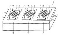
本発明の発光装置1において、発光素子5は、直線状の各配線パターンを挟んで、配線パターンに沿って直線状に複数個搭載されてなることが好ましい。本発明の発光装置における配線パターンの数は、特に制限されるものではないが、アノード用配線パターン、カソード用配線パターンがそれぞれ1本以上必要であるため、少なくとも2本以上の配線パターンが必要であり、2〜4本の範囲内が好ましい。発光装置から電流350mAの時に全光束を300lmを得るためには、発光素子が36個必要となる。その場合、たとえば配線パターン4は、4つの配線パターン4a,4b,4c,4dを有するように形成され、配線パターン4a,4b間に12個、配線パターン4b,4c間に12個、配線パターン4c,4d間に12個の発光素子5がそれぞれ搭載される(図1〜図3に示す例)。 In the light-emitting
なお、図1〜図3には、発光装置1が正方形状の上面形状を有するように実現された例を示しているが、この場合には、図3に示すように、直線状の配線パターン4は、発光装置1の上面形状である正方形状の対角線の1つに平行になるように形成されてなることが好ましい。このように配線パターン4が形成されてなることで、配線パターン4の長さおよび間隔を十分に確保することができ、また後述する発光装置の固定用穴、外部配線用穴などを形成できる領域も確保できるというような利点がある。なお、上述した発光装置の上面形状とは、絶縁基板3の基板面に平行な断面における形状を意味する。1 to 3 show an example in which the light-emitting
また本発明の発光装置1において、配線パターン4を挟んで搭載された各発光素子5は、側面同士が対向しないようにずらして配置されていることが好ましい。このように発光素子5が配置されていることで、輝度が均一となり、輝度ムラを低減できるという利点がある。 Moreover, in the light-emitting
また本発明の発光装置1においては、発光素子5は上面形状が長方形状の発光素子を用いることが好ましい。ここで、発光素子5の上面形状は、絶縁基板3上に搭載された状態での当該絶縁基板3の基板面に平行な上面における形状を指す。このような上面形状が長方形状の発光素子5として、具体的には、当該上面形状における短辺が200〜300μmの範囲内であり、長辺が400〜1000μmの範囲内である発光素子が例示される。本発明の発光装置1では、このような上面形状が長方形状の発光素子5を用いる場合には、当該発光素子5の上面形状の短辺に沿った方向が配線パターン4の長手方向と平行となるように搭載されていることが好ましい。通常、上面形状が長方形状の発光素子5においては、その上面の短辺側に電極パッドが形成されているため、上述のように発光素子5を搭載することで、ボンディングワイヤWを用いた発光素子5の電極パッドと配線パターン4との間の電気的接続を容易に行うことができ、ボンディングワイヤWの切断、ボンディングワイヤWの剥れなどの不良を防止することができる。また、このようにすることで、配線パターン4の長手方向に沿って所望の間隔、所望の数だけ発光素子5を搭載することにより所望の光が得られるよう容易に調整することができるという利点がある。In the
上述のように本発明に用いる発光素子5は、長方形状の上面形状を有する発光素子を用いることが好ましいが、上述したような発光素子の上面の短辺側に通常電極パッドが形成されていることにより、ボンディングワイヤWを用いた配線パターン4との間の電気的接続が容易であり、ボンディングワイヤWの切断、剥れなどの不良の防止の効果が特に顕著であることから、長尺状の上面形状を有する発光素子を用いることがより好ましい。ここで、「長尺状」とは、上面形状における短辺の長さに対し長辺の長さが顕著に長い形状を指し、たとえば、長辺が480μmであり、短辺が240μmであるような上面形状を有する発光素子が例示される。長尺状の上面形状を有する発光素子を用いる場合には、電極パッドが短辺の端(短辺側)に設けられ、電極パッドが対向するように設けられた発光素子を用いることが好ましい。As described above, the light-emitting
なお、本発明の発光装置1において、平行に配置された複数の直線状の配線パターン4と、複数個の発光素子5との間をどのように電気的に接続するかは特に制限されるものではなく、直線状の配線パターン4を挟んで搭載された発光素子5同士は、直列に電気的に接続されていてもよいし、並列に電気的に接続されていてもよい。直線状の配線パターン4を挟んで搭載された発光素子5同士が直列に電気的に接続され、直線状の配線パターンに沿って直線状に搭載された発光素子5同士が並列に電気的に接続されていてもよい。なお、発光素子と電極との距離は近い方が配線の抵抗による電圧降下が最も小さくなるので好ましい。さらに、配線パターンに沿って直線状に配列されて複数個搭載されている発光素子は全て電極と電気的に接続するのではなく、一部の発光素子は予備の発光素子として搭載しただけの状態にしておくことが好ましい。このようにすることで、発光素子を封止体で封止する前の検査工程(後述)で故障して発光しない発光素子があることが分かった場合に、予備の発光素子を電極と電気的に接続して所定の明るさとすることができる。 In the
本発明の発光装置はまた、配線パターンが、発光素子との間の電気的接続の位置決め用のパターン、または、発光素子の搭載位置の目安用のパターンをさらに有することが、好ましい。図3には、平行に形成された4つの直線状の配線パターン4に繋がって、パターン7が点在して形成された例を示している。このパターン7を、配線パターン4と発光素子5との間の電気的接続の位置決め、または、発光素子5の搭載位置の目安として用いることで、発光素子の搭載および配線パターンとの間の電気的接続が容易となり、さらに自動化装置を用いる場合の認識パターンとして用いることもできるという利点がある。 In the light emitting device of the present invention, it is also preferable that the wiring pattern further has a pattern for positioning electrical connection with the light emitting element or a pattern for indicating the mounting position of the light emitting element. FIG. 3 shows an example in which four
本発明の発光装置1では、発光素子5と配線パターン4との間の直線距離が0.1mm以上であることが好ましく、0.5mm以上であることがより好ましい。ここで、この直線距離は、絶縁基板3の基板面に沿った方向における発光素子5と配線パターン4との間の直線距離を意味する。上記直線距離が0.1mm以上であることで、電気的絶縁性が確実に達成される。なお、ワイヤボンディングの際のタレ、ボンディングワイヤの切断防止の観点からは、発光素子5と配線パターン4との間の水平方向に沿った直線距離は、1.5mm以下であることが好ましく、1.0mm以下であることがより好ましい。 In the
本発明の発光装置1はまた、図2に示すように、配線パターン4の厚みは、発光素子の厚みよりも小さいことが好ましい。これによって、発光素子5から発光する光を、配線パターンによって外部に放出される光が遮蔽することが低減され、外部に効率よく光を放出できる発光装置1が実現できる。具体的には、配線パターン4の上記領域の厚みと発光素子5の厚みとの差は、0.005mm以上であることが好ましく、0.07mm以上であることがより好ましい。 In the
本発明の発光装置1における絶縁基板3は、絶縁性を有する材料で形成されていればよく、特に制限されるものではないが、熱膨張が小さく、熱伝導性が高く、かつ光反射率が高いことから、白色のセラミック基板であることが好ましい。ここで、「白色」とは、物体が全ての波長の可視光線をほぼ100%反射するような物体の色を指す(ただし、100%の反射率をもった理想的な白色の物体は存在しない。)。白色のセラミック基板を絶縁基板3として用いることで、発光素子5からの出射光のうち、特に下面方向への光を白色のセラミック基板にて反射することができ、発光素子5からの出射光をロスなく有効に活用できるとともに、高い放熱性および耐熱性が要求される駆動電流として大電流を供給する用途にも好適に適用することができる。さらに、発光素子5の信頼性を向上できるとともに、封止体6が蛍光体を含有する場合(後述)には、発光素子5からの熱による蛍光体の劣化を抑えることもでき、蛍光体により波長変換されて出光する光の色度ズレが生じにくい。またさらに、上述のように光反射率の高いセラミック基板を用いることで、基板材料および/または配線パターンの形成材料に光反射率90%以上の銀を用いる必要がないため、銀マイグレーションの心配がなく、さらに銀が硫化してしまう問題もない。 The insulating
白色のセラミック基板を用いる場合には、光反射率が90%以上と高いことから、酸化アルミニウム(アルミナ)、窒化アルミニウム、ボロンナイトライド、窒化ケイ素、酸化マグネシウム、フォルステライト、ステアタイト、低温焼結セラミックから選ばれるいずれか、または、これらの複合材料で形成されたセラミック基板が好ましい。上述した中でも、安価で、反射率が高く、加工しやすく、工業材料として広く使われている酸化アルミニウム(アルミナ)で形成された白色のセラミック基板が特に好ましい。 When using a white ceramic substrate, the light reflectivity is as high as 90% or more, so aluminum oxide (alumina), aluminum nitride, boron nitride, silicon nitride, magnesium oxide, forsterite, steatite, low temperature sintering Any one selected from ceramics or a ceramic substrate formed of these composite materials is preferable. Among these, a white ceramic substrate made of aluminum oxide (alumina), which is inexpensive, has high reflectance, is easy to process, and is widely used as an industrial material, is particularly preferable.
本発明の発光装置1に用いられる発光素子5としては、当分野において通常用いられる発光素子を特に制限なく用いることができる。このような発光素子としては、たとえば、サファイヤ基板、ZnO(酸化亜鉛)基板、GaN基板、Si基板、SiC基板、スピネルなどの基板上に、窒化ガリウム系化合物半導体、ZnO(酸化亜鉛)系化合物半導体などの材料を成長させた青色系LED(発光ダイオード)チップ、InGaAlP系化合物半導体LEDチップ、AlGaAs系化合物半導体LEDチップなどの半導体発光素子を挙げることができる。中でも、絶縁性基板に片面2電極構造を容易に作製でき、結晶性のよい窒化物半導体を量産性よく形成できることから、サファイヤ基板上に窒化ガリウム系化合物半導体を成長させた青色系LEDを発光素子として用いることが、好ましい。このような青色系LEDを発光素子として用いる場合には、当該半導体発光素子からの光で励起されて黄色系の光を発する蛍光体を封止体中に分散させることで、白色を得るように発光装置を実現することが好ましい(後述)。 As the
なお、本発明の発光装置に用いられる発光素子は、発光色は青色発光に限定されるものではなく、たとえば紫外線発光、緑色発光などの発光色の発光素子を用いても勿論よい。また、青色系LEDを発光素子として用い、この青色系LEDから発せられる光を蛍光体によって変換して白色を得る構成に換えて、蛍光体を用いずにたとえば赤、緑、青の三色のLEDチップをそれぞれ発光素子として用いて、白色などの照明に必要な色が得られるように発光装置を実現するようにしても勿論よい。 Note that the light-emitting element used in the light-emitting device of the present invention is not limited to blue light emission, and for example, a light-emitting element having a light emission color such as ultraviolet light emission or green light emission may be used. In addition, instead of using a blue LED as a light emitting element and converting the light emitted from the blue LED by a phosphor to obtain white, for example, three colors of red, green, and blue are used without using the phosphor. Of course, the light emitting device may be realized by using each LED chip as a light emitting element so as to obtain a color necessary for illumination such as white.
本発明の発光装置1に用いられる発光素子5は、その形状については特に制限されるものではないが、上述したように、上面形状が長方形状であることが好ましく、長尺状であることがより好ましい。なお、本発明の発光装置1においては、一方の面にP側電極およびN側電極が形成された発光素子5を用いる必要がある。このような発光素子5を、P側電極およびN側電極が形成された面を上面として絶縁基板3上の配線パターン4の間に搭載し、配線パターン4との間を電気的に接続する。The shape of the light-emitting
発光素子5と配線パターン4との電気的接続は、図2に示すように、P側電極およびN側電極をそれぞれ配線パターン4にボンディングワイヤWをボンディングすることで実現される。ボンディングワイヤWとしては、当分野において従来から広く用いられている適宜の金属細線を特に制限されることなく用いることができる。このような金属細線としては、たとえば金線、アルミニウム線、銅線、白金線などが挙げられるが、中でも腐食が少なく、耐湿性、耐環境性、密着性、電気伝導性、熱伝導性、伸び率が良好であり、ボールが出来やすいことから、金線をボンディングワイヤWとして用いることが好ましい。 As shown in FIG. 2, the electrical connection between the light emitting
本発明の発光装置1は、上述したように配線パターン4の間に、配線パターン4に電気的に接続された状態で搭載された複数個の発光素子5を、電気的接続を行っているボンディングワイヤWごと、封止体6にて封止してなる。封止体6による封止は、直線状の配線パターン4に沿って両側に搭載された発光素子5を含むように直線状の封止体を複数形成するようにしてもよいし、絶縁基板上の直線状の配線パターンおよび発光素子の全てを1つの封止体で封止するようにしてもよい。発光装置の輝度ムラを低減でき、封止体の厚みのバラツキを低減できる観点からは、図1〜図3に示す例のように、絶縁基板上の直線状の配線パターンおよび発光素子の全てを1つの封止体で封止することが好ましい。In the
本発明の発光装置1における封止体6を形成するための材料(封止材料)としては、透光性を有する材料であれば特に制限されるものではなく、当分野において従来から広く知られた適宜の材料を用いて形成することができる。このような封止材料としては、たとえば、エポキシ樹脂、ユリア樹脂、シリコーン樹脂などの耐候性に優れた透光性樹脂材料、耐光性に優れたシリカゾル、硝子などの透光性無機材料が好適に用いられる。 The material (sealing material) for forming the sealing
本発明における封止体6は、所望の光が得られるように調整可能であり、また、白色、昼白色、電球色などが容易に得られることから、蛍光体を含有してなることが好ましい。蛍光体としては、たとえば、Ce:YAG(セリウム賦活イットリウム・アルミニウム・ガーネット)蛍光体、Eu:BOSE(ユーロピウム賦活バリウム・ストロンチウム・オルソシリケート)蛍光体、Eu:SOSE(ユーロピウム賦活ストロンチウム・バリウム・オルソシリケート)蛍光体、ユーロピウム賦活αサイアロン蛍光体などを好適に用いることができるが、これらに制限されるものではない。 The sealing
なお、本発明における封止体6には、蛍光体と共に拡散剤を含有させるようにしてもよい。拡散剤としては、特に制限されるものではないが、たとえば、チタン酸バリウム、酸化チタン、酸化アルミニウム、酸化珪素、炭酸カルシウム、二酸化珪素などが好適に用いられる。 In addition, you may make it make the sealing
本発明における封止体6は、発光装置1の所望される光の色度に応じて、2層で実現することができる。この場合、図2に示すように第1の蛍光体を含有する第1の封止体層8と、第1の封止体層8上に積層された第2の蛍光体を含有する第2の封止体層9とを備えるように実現されることが好ましい。このように封止体6を第1の封止体層8と第2の封止体層9とで構成することで、色度を容易に調整でき、色度ズレのない発光装置を、良好な歩留りで安価に提供することができるという利点がある。好適な具体例としては、樹脂材料としてメチルシリコーンを用い、これに第1の蛍光体としてEu:BOSEを分散させ、硬化させることにより第1の封止体層8を形成し、この第1の封止体層8を覆うようにして、樹脂材料として有機変性シリコーンを用い、これに第2の蛍光体としてEu:SOSEを分散させ、硬化させることにより第2の封止体層9を形成する場合が例示される。色度ズレの調色の観点からは、第2の封止体層9は、第1の封止体層8の上面の少なくとも一部を覆うようにして第1の封止体層8上に積層されていることが好ましく、図2に示すように第1の封止体層8の上面の全面を第2の封止体層9で覆うようにして実現されることが特に好ましい。なお、1層(第1の蛍光体層)のみで所望の色度の光を発する発光装置が得られる場合には、封止体6は単層で実現されても勿論よい。ここで、第1の蛍光体を含有する第1の封止体層8と、第2の蛍光体を含有する第2の封止体層9の境界は、明確に分離していても、明確に分離していなくともよい。The sealing
本発明における封止体6は、その形状については特に制限されるものではないが、六角形状、円形状、長方形状または正方形状の上面形状を有することが好ましい。図1〜図3には、第1の封止体層8を正方形状の上面形状を有するように形成し、この第1の封止体層8の上面の全面を覆うようにして正方形状の上面形状を有するように第2の封止体層9を形成してなる例を示している。なお、上述した封止体6、第1の封止体層8および第2の封止体層9の上面形状とは、絶縁基板3の基板面に平行な断面における形状を指す。The shape of the sealing
ここで、図4は、本発明の好ましい第2の例の発光装置21の上面図である。図4に示す例の発光装置21は、封止体22の上面形状が円形状であることを除いては図1に示した例の発光装置1と同様の構成を有するものであり、同様の構成を有する部分については同一の参照符を付して説明を省略する。図4に示すように封止体22が円形状の上面形状を有するように実現されることで、対称形状であるため光指向性がよいという利点がある。このため、上述した六角形状、円形状、長方形状または正方形状の中でも、図4に示すように円形状の上面形状を有するように封止体22を実現することが特に好ましい。Here, FIG. 4 is a top view of the
また封止体6は、上方に凸となる半球状に形成するようにしてもよい。この場合には、封止体6にレンズとしての機能を持たせることも可能になる。 Moreover, you may make it form the sealing
本発明の発光装置1は、その全体の形状についても特に制限されるものではないが、六角形状、円形状、長方形状または正方形状の上面形状を有するように実現されることが好ましい。発光装置が長方形状または正方形状の上面形状を有する場合には、発光素子を密着させて配置することができるため、発光装置を蛍光灯型LEDランプに適用する場合に特に好ましい。また、発光装置を電球型LEDランプ(後述)に適用する場合には、発光装置が円形状の上面形状を有するように実現されることが好ましい。図1および図4には、上述のように発光装置1が正方形状の上面形状を有するように実現された例を示している。The
また図5は、本発明の好ましい第3の例の発光装置31の上面図である。図5に示す例の発光装置31は、封止体33の上面形状が六角形状であり、発光装置31の上面形状が円形状であることを除いては図1に示した例の発光装置1と同様の構成を有するものであり、同様の構成を有する部分については同一の参照符を付して説明を省略する。図5に示す例の発光装置31のように封止体33を六角形状の上面形状を有するように実現することでも、対称形状であるため、光の指向性がよいという利点がある。また、図5に示す例のように円形状の上面形状を有する(円形状の上面形状を有する絶縁基板32を用いる)された発光装置31は、電球型LEDランプに特に好適に適用できる。FIG. 5 is a top view of the
図6は、本発明の好ましい第4の例の発光装置41の上面図である。図6に示す例の発光装置41は、封止体42(第1の封止体層43)の上面形状が円形状であり、第2の封止体層44が第1の封止体層43の上面の一部のみを覆うように形成されていることを除いては図5に示した例の発光装置31と同様の構成を有するものであり、同様の構成を有する部分については同一の参照符を付して説明を省略する。図6に示す例の発光装置41のように封止体42を円形状の上面形状を有するように実現することで、対称形状であるため、光の指向性がよいという利点がある。また図6に示す例では、円形状の上面形状を有するように形成された第1の封止体層43と、この第1の封止体層43を部分的に覆うようにして形成された第2の封止体層44とで封止体42が形成されている。このように第1の封止体層43を部分的に覆うようにして第2の封止体層44を形成することで、第1の封止体層の一部のみの調整で発光装置として所望の色度特性を有する(たとえば、後述する色度座標を示す図13の(b)の範囲内に入る)発光装置を得ることができるという利点がある。なお、このような場合、第2の封止体層44にて覆う第1の封止体層43の部分は、所望の色度特性に応じて選択する(たとえば、後述する色度座標を示す図13の(b)の範囲内に入っていない部分など)。また図6に示す例の発光装置41は、円形状の上面形状を有するため、図5に示した例の発光装置31と同様に電球型LEDランプに特に好適に適用できる。FIG. 6 is a top view of a
図7は、本発明の好ましい第5の例の発光装置51の上面図である。図7に示す例の発光装置51は、封止体52(第1の封止体層53)の上面形状が正方形状であり、第2の封止体層44が第1の封止体層53の上面の一部のみを覆うように形成されていることを除いては図5に示した例の発光装置31と同様の構成を有するものであり、同様の構成を有する部分については同一の参照符を付して説明を省略する。図7に示す例の発光装置51のように封止体52(第1の封止体層53)を正方形状の上面形状を有するように実現することで、後述する固定用穴、外部配線用穴などを形成できる領域を確保できるという利点がある。また図7に示す例では、正方形状の上面形状を有するように形成された第1の封止体層53と、この第1の封止体層53を部分的に覆うようにして形成された第2の封止体層44とで封止体42が形成されており、これによって図6に示した例と同様の効果が奏される。また図7に示す例の発光装置51は、円形状の上面形状を有するため、図5、図6に示した例の発光装置31,41と同様に電球型LEDランプに特に好適に適用できる。上記第1の封止体層43、第1の封止体層53は第1の蛍光体を含有し、第2の封止体層44は第2の蛍光体を含有する。FIG. 7 is a top view of a
本発明の発光装置は、製造方法が容易で、色ズレが発生しにくい発光装置が提供でき、このことから、液晶ディスプレイのバックライト光源または照明用光源に特に好適に用いられる。本発明の発光装置を用いることで、白色を含め電球色など任意の色調の上記光源を実現できる。 The light-emitting device of the present invention can provide a light-emitting device that is easy to manufacture and is less likely to cause color misregistration, and is therefore particularly suitable for a backlight light source or an illumination light source for a liquid crystal display. By using the light emitting device of the present invention, the light source having an arbitrary color tone such as a light bulb color including white can be realized.
本発明の発光装置は、通常、上述した用途に供するために、相手部材に取り付け、固定するための固定用穴を有する。図1および図4に示した正方形状の上面形状を有する発光装置1,21では、正方形状の上面形状を有する絶縁基板3の対向する角部に、絶縁基板3を貫通するように設けられた固定用穴11が対角線上に配置されて1つずつ形成された場合を示している。また、図5〜図7に示した円形状の上面形状を有する発光装置31,41,51では、切り欠き状の固定用穴34が、円形状の上面形状を有する絶縁基板32の中心を通る直線上に配置されて1つずつ形成された例を示している。The light-emitting device of the present invention usually has a fixing hole for attaching and fixing to a counterpart member in order to provide the above-described use. In the
また本発明の発光装置は、上述した用途に供するために、固定用冶具を用いて相手部材に取り付けられ、固定される。この固定用冶具としては、たとえば図1および図4に示す固定用冶具19のように、内壁にネジ山が形成された固定用穴11に挿入され、螺合するネジなどが挙げられる。また固定用冶具は、接着シートなどであってもよい。Moreover, in order to use for the use mentioned above, the light-emitting device of this invention is attached and fixed to a counterpart member using a fixing jig. Examples of the fixing jig include a screw that is inserted into the fixing
本発明の発光装置においては、絶縁基板と同じ材料で形成された固定用冶具を用いて固定されてなることが好ましい。絶縁基板と同じ材料で形成された固定用冶具を用いることで、絶縁基板と固定用冶具との熱膨張率を同じにすることができ、熱による反りなどで絶縁基板に割れ、ヒビは発生することを低減でき、発光装置の歩留りを向上することができる。具体的には、酸化アルミニウム、窒化アルミニウム、ボロンナイトライド、窒化ケイ素、酸化マグネシウム、フォルステライト、ステアタイト、低温焼結セラミックから選ばれるいずれか、または、これらの複合材料で形成された固定用冶具を、絶縁基板の形成材料に合わせて好適に用いることができる。 In the light emitting device of the present invention, it is preferable that the light emitting device is fixed using a fixing jig formed of the same material as the insulating substrate. By using a fixing jig made of the same material as the insulating substrate, the thermal expansion coefficient of the insulating substrate and the fixing jig can be made the same, and the insulating substrate is cracked and cracked due to heat warpage. This can be reduced and the yield of the light-emitting device can be improved. Specifically, a fixing jig formed of any one selected from aluminum oxide, aluminum nitride, boron nitride, silicon nitride, magnesium oxide, forsterite, steatite, low-temperature sintered ceramic, or a composite material thereof. Can be suitably used according to the forming material of the insulating substrate.
ここで、図8〜図10には、本発明の発光装置を照明用光源として適用した例をそれぞれ示している。図8は、図1に示した例の発光装置1を蛍光灯型LEDランプ61に適用した場合を示す斜視図であり、図9は、図6に示した例の発光装置41を蛍光灯型LEDランプ71に適用した場合(第1の蛍光体層43を部分的に覆う第2の蛍光体層44については省略している)を示す斜視図であり、図10は、図6に示した例の発光装置41を電球型LEDランプ81に適用した場合を示す断面図である。図8〜図10に示すように、発光装置1,41は、それぞれ固定用穴11,34で、固定用冶具19を用いて取り付けられ、固定される。 Here, FIGS. 8 to 10 show examples in which the light-emitting device of the present invention is applied as a light source for illumination. FIG. 8 is a perspective view showing a case where the
なお、本発明の発光装置は、図1、図4〜図7にそれぞれ示されているように、絶縁基板3,32上に、正電極外部接続ランド12および負電極外部接続ランド13が直接設けられ、この正電極外部接続ランド12および負電極外部接続ランド13と電源(図示せず)との間をそれぞれ電気的に接続するための外部接続配線14が設けられてなることが好ましい。 In the light emitting device of the present invention, as shown in FIGS. 1 and 4 to 7, the positive electrode
また本発明の発光装置は、図1、図4〜図7にそれぞれ示されているように、絶縁基板3,32に、外部接続配線14を通すための外部配線用穴15が形成されてなることが好ましい。図1および図4に示す例では、正方形状の上面形状を有する絶縁基板3に、上述した固定用穴11が設けられている対角線上とは異なるもう1つの対角線上に配置されるように正電極外部接続ランド12および負電極外部接続ランド13が設けられており、さらに絶縁基板3の対向する2つの辺の中央付近に切り欠き状の外部配線用穴15が形成されている。また、図5〜図7に示す例では、円形状の上面形状を有する絶縁基板32上に、上述したように固定用穴34が形成された中心を通る直線上に概ね垂直な中心を通る直線上に、切り欠き状の外部配線用穴15が形成され、この固定用穴34と外部配線用穴15との間に、対向して正電極外部接続ランド12および負電極外部接続ランド13が設けられている。なお、図4〜図7に示す例のように円形状の上面形状を有する絶縁基板32に固定用穴34および外部配線用穴15を切り欠き状に形成した場合には、相手部材に取り付けられた状態で、発光装置が周方向に回るのを防止する、回り止めの役割も果たす。Further, the light emitting device of the present invention is formed by forming external wiring holes 15 through the insulating
また、本発明の発光装置は、図3に示すように、絶縁基板3上に、配線パターン4の一端と正電極外部接続ランド12および負電極外部接続ランド13との間を電気的に接続するための外部引き出し配線パターン16,17がさらに形成されていることが好ましい。このような外部引き出し配線パターン16,17により、電源(図示せず)と配線パターン4との間を、正電極外部接続ランド12および外部引き出し配線パターン16、負電極外部接続ランド13および外部引き出し配線パターン17をそれぞれ介して、電気的に接続することができる。 Further, as shown in FIG. 3, the light emitting device of the present invention electrically connects one end of the
さらに本発明の発光装置は、絶縁基板上に、検査用のパターンがさらに形成されてなるのが好ましい。図3には、配線パターン4aと配線パターン4bとの間、配線パターン4cと配線パターン4dとの間にそれぞれスポット状の検査用のパターン18が形成された例を示している。このような検査用のパターン18が絶縁基板3上に形成されていることで、配線パターン4aと配線パターン4bとの間、配線パターン4bと配線パターン4cとの間および配線パターン4cと配線パターン4dとの間の導通の検査を検査用のパターン18を介して容易に行うことができるようになる。また、この検査用のパターン18は、ダイボンド、ワイヤボンディングを自動化装置で行う際の認識パターンとしても用いることができる。なお、検査用のパターンは、図3に示したようなスポット状に限定されるものではなく、配線パターン4bと配線パターン4cとそれぞれ電気的に繋がっておりプローブを当てられる大きさのパターンにて実現されてもよい。 In the light emitting device of the present invention, it is preferable that an inspection pattern is further formed on the insulating substrate. FIG. 3 shows an example in which spot-shaped
本発明はまた、発光装置の製造方法についても提供する。上述してきた本発明の発光装置は、その製造方法については特に制限されるものではないが、本発明の発光装置の製造方法を適用することで好適に製造することができる。本発明の発光装置の製造方法は、絶縁基板上に配線パターンを形成する工程と、配線パターン間に発光素子を搭載する工程と、発光素子と配線パターンとを電気的に接続する工程と、貫通孔を有するシリコーンゴムシートを絶縁基板上に載置する工程と、シリコーンゴムシートの貫通孔内に、発光素子を封止する封止体を形成する工程とを基本的に含む。ここで、図11は、本発明の発光装置の製造方法の好ましい一例として、図1に示した発光装置1を製造する場合を段階的に示す図である。以下、図11を参照して、本発明の発光装置の製造方法について具体的に説明する。 The present invention also provides a method for manufacturing a light emitting device. The manufacturing method of the light emitting device of the present invention described above is not particularly limited, but can be preferably manufactured by applying the manufacturing method of the light emitting device of the present invention. A method of manufacturing a light emitting device according to the present invention includes a step of forming a wiring pattern on an insulating substrate, a step of mounting a light emitting element between the wiring patterns, a step of electrically connecting the light emitting element and the wiring pattern, and a penetration The method basically includes a step of placing the silicone rubber sheet having holes on the insulating substrate and a step of forming a sealing body for sealing the light emitting element in the through hole of the silicone rubber sheet. Here, FIG. 11 is a diagram showing step by step a case where the
まず、図11(a)に示すように、絶縁基板3上に、配線パターン4を形成する。上述したように図11は図1に示した発光装置1を製造する場合であるので、配線パターン4として、4つの直線状の配線パターン4a,4b,4c,4dを平行に配置して絶縁基板3上に形成する。好適な具体例として、厚み1mmの酸化アルミニウムで形成された白色の絶縁基板3上に、厚み0.07mmの金膜をスパッタリング法を用いて形成した後、フォトエッチング法にて配線パターン4a,4b,4c,4d(幅1mm、間隔2mm)を形成する場合が挙げられるが、これに限定されるものではない。なお、上述したように発光素子との間の電気的接続の位置決め用または発光素子の搭載位置の目安用のパターン7として直線から外側に膨らんだパターン、外部引き出し配線パターン16,17、検査用のパターンを形成する場合には、所望のパターンとなるように設計してフォトエッチングを行えばよい。 First, as shown in FIG. 11A, the
次に、図11(b)に示すように、配線パターン4間に発光素子5を搭載する。ここで、発光素子5の搭載は、たとえばエポキシ樹脂、アクリル樹脂、イミド樹脂などの熱硬化性樹脂を用いて発光素子5を絶縁基板3に直に接着することで行うことができる。そうすることにより、沿面放電電圧で決まる絶縁耐圧をできる限り高くすることができる。すなわち、電極方向に配列された発光素子と発光素子との間の絶縁耐圧は発光素子間の距離と絶縁基板の誘電率で決まり、発光素子と電極との間の絶縁耐圧も同様に発光素子と電極との最短距離と絶縁基板の誘電率で決まる。好適な具体例としては、絶縁基板3上に平行に形成された直線状の配線パターン4a,4b,4c,4dのそれぞれの間に、発光素子5として短辺幅0.24mm、長辺0.48mm、厚み0.14mmのLEDチップをエポキシ樹脂を用いて接着し、固定する場合が挙げられるが、これに限定されるものではない。その後、図11(b)に示すように、所望の電気的接続の状態に応じて、配線パターン4と発光素子5とをワイヤボンディングWを用いて電気的に接続する。 Next, as shown in FIG. 11B, the
なお、本発明の発光装置の製造方法では、上述のように発光素子と配線パターンとを電気的に接続した後に、発光素子の特性を検査する工程と、検査の結果、特性不良があった場合に、予備の発光素子を配線パターンと接続する工程とをさらに含むことが好ましい。この検査は、たとえば発光素子に電流を流し、その光出力特性を測定することで行なうことができる。また、外観検査としてボンディングワイヤWの断線、ボンディング不良も併せて行なうようにしてもよい。 In the method for manufacturing a light emitting device according to the present invention, after the light emitting element and the wiring pattern are electrically connected as described above, the characteristics of the light emitting element are inspected. It is preferable that the method further includes a step of connecting the spare light emitting element to the wiring pattern. This inspection can be performed, for example, by passing a current through the light emitting element and measuring its light output characteristics. Further, as an appearance inspection, disconnection of the bonding wire W and bonding failure may be performed together.
次に、図11(c)に示すように、貫通孔92を有するシリコーンゴムシート91を絶縁基板3上に載置する。ここで、図12は、本発明の発光装置の製造方法において用いられる、好ましい一例のシリコーンゴムシート91を模式的に示す図である。本発明の製造方法に用いるシリコーンゴムシートは、封止体を形成するための空間となる貫通孔を有するものを用いるが、この貫通孔の形状については特に制限されるものではなく、形成しようとする封止体の上面形状に応じた形状のものを用いることができる。上述したように、封止体は、六角形状、円形状、長方形状または正方形状の上面形状を有することが好ましいため、シリコーンゴムシート91の貫通孔は、六角形状、円形状、長方形状または正方形状の上面形状を有することが好ましい。図12には、一例として、長方形状の上面形状を有する貫通孔92を有するシリコーンゴムシート91を示している。なお、上述したような貫通孔92を有するシリコーンゴムシート91は、絶縁基板上の直線状の配線パターンおよび発光素子の全てを1つの封止体で封止する場合に特に好適に用いることができるが、直線状の配線パターン4に沿って両側に搭載された発光素子5を含むように直線状の封止体を複数形成する場合には、対応する複数個の所望の形状の貫通孔を有するシリコーンゴムシートを用いるようにすればよい。Next, as shown in FIG. 11C, a
シリコーンゴムシート91は、容易に入手可能であり、ゴム製であるため弾性を有し、配線パターンなどの段差があっても隙間なく密着させて設けることができ、好ましい。また、シリコーンゴムシート91には、絶縁基板3に設けた状態では後述する封止体形成用の樹脂の漏れを防ぐことができ、また、封止体形成後に容易に除去できることから、一面に両面接着シートを接着しておき、この接着シートで絶縁基板3に接着させるようにすることが好ましい。 The
本発明の発光装置の製造方法に用いるシリコーンゴムシートは、その厚みが、形成する第1の封止体層の厚みの2倍以上であることが好ましい。シリコーンゴムシートが、第1の封止体層の厚みの2倍以上の厚みを有することで、色度ズレを修正するために2度塗りができ、封止材料の漏れを防止できるという利点がある。 The thickness of the silicone rubber sheet used in the method for manufacturing a light emitting device of the present invention is preferably at least twice the thickness of the first encapsulant layer to be formed. Since the silicone rubber sheet has a thickness that is twice or more the thickness of the first sealing body layer, the silicone rubber sheet can be applied twice to correct the chromaticity deviation, thereby preventing the leakage of the sealing material. is there.
次に、図11(d)に示すように、シリコーンゴムシート91の貫通孔92内に、発光素子5を封止する封止体6を形成する。ここで、封止体6には、上述のように蛍光体を含有させることが、好ましい。また、封止体6は単層、二層のいずれの形態で形成するようにしてもよい(図11は、図1に示した発光装置1を製造する場合であるため、第1の蛍光体を含有する第1の封止体層8と、第2の蛍光体を含有する第2の封止体層9とを有するように封止体6を形成する場合を示している。 Next, as illustrated in FIG. 11D, a sealing
本発明の発光装置の製造方法におけるこの封止体で発光素子を封止する工程は、シリコーンゴムシートの貫通孔内に第1の蛍光体を含有する封止材料を注入する工程と、第1の蛍光体を含有する樹脂を硬化させて第1の封止体層を形成する工程と、第1の封止体層形成後の発光装置の色度特性を測定する工程とを含むことが、好ましい。 The step of sealing the light emitting element with this sealing body in the method for manufacturing the light emitting device of the present invention includes the step of injecting a sealing material containing the first phosphor into the through hole of the silicone rubber sheet, Including a step of curing the resin containing the phosphor and forming the first encapsulant layer, and a step of measuring the chromaticity characteristics of the light emitting device after the formation of the first encapsulant layer. preferable.
この場合、まず、シリコーンゴムシート91の貫通孔92内に第1の蛍光体を含有する封止材料を注入する。ここで、封止材料としては、上述したようにたとえば、エポキシ樹脂、ユリア樹脂、シリコーン樹脂などの耐候性に優れた透光性樹脂材料、耐光性に優れたシリカゾル、硝子などの透光性無機材料が好適に用いられる。また、第1の蛍光体としては、上述したようにたとえば、Ce:YAG蛍光体、Eu:BOSEあるいはEu:SOSE蛍光体、ユーロピウム賦活αサイアロン蛍光体などを好適に用いることができる。また、封止材料には上述した拡散剤が添加されていてもよい。In this case, first, a sealing material containing the first phosphor is injected into the through
次に、シリコーンゴムシート91の貫通孔92内に注入された第1の蛍光体を含有する封止材料を硬化させる。封止材料を硬化させる方法としては、用いる封止材料に応じて従来公知の適宜の方法を特に制限されることなく用いることができる。たとえば封止材料として透光性樹脂材料であるシリコーン樹脂を用いる場合には、シリコーン樹脂を熱硬化させることで、封止材料を硬化させることができる。なお、封止材料としてモールド用の樹脂を用い、金型を用いて封止材料を硬化させるようにしてもよい。封止材料の硬化により形成される封止体(第1の封止体層)の形状は特にされるものではなく、たとえば上方に凸となる半球状の形状に封止体を形成することで、封止体にレンズとしての機能を持たせるようにしてもよい。 Next, the sealing material containing the first phosphor injected into the through
次に、上述のようにして第1の封止体層を形成した後の発光装置の色度特性を測定する。ここで、図13はCIEの色度座標を示すグラフである。発光装置の色度特性は、JIS28722の条件C,DIN5033teil7、ISOk772411に準拠のd・8(拡散照明・8°受光方式)光学系を採用した測定装置を用いて測定することができる。たとえば、CIEの色度表でx、y=(0.325、0.335)となる光を発するように、第1の蛍光体と封止材料であるシリコーン樹脂とを5:100の重量比で混合したものをシリコーンゴムシート91の貫通孔92内に注入し、150℃の温度で30分間熱硬化させて第1の封止体層を形成した場合、形成された第1の封止体層の色度範囲は、図13中の(a)の領域内となる。このような第1の封止体層を有する発光装置について色度特性を測定する場合には、色度範囲は図13中の(b)の領域から外れてしまう。このような場合には、発光装置の色度範囲が図13中の(b)の領域内となるように、第1の封止体層上に第2の封止体層を形成する。 Next, the chromaticity characteristics of the light emitting device after forming the first sealing body layer as described above are measured. Here, FIG. 13 is a graph showing CIE chromaticity coordinates. The chromaticity characteristics of the light emitting device can be measured by using a measuring device employing a d · 8 (diffuse illumination · 8 ° light receiving method) optical system in accordance with JIS 28722, Condition C, DIN5033tail7 and ISOk772411. For example, the weight ratio of the first phosphor and the silicone resin as the sealing material is 5: 100 so as to emit light with x, y = (0.325, 0.335) in the CIE chromaticity table. When the first sealing body layer is formed by injecting the mixture in the through
第2の封止体層を形成する場合、本発明の発光装置の製造方法は、上述した第1の封止体層形成後の発光装置の色度特性を測定する工程の後に、第1の封止体層上に、第2の蛍光体を含有する封止材料を注入する工程と、第2の蛍光体を含有する封止材料を硬化させて第2の封止体層を形成する工程と、第2の封止体層形成後の発光装置の色度特性を測定する工程と、シリコーンゴムシートを除去する工程とをさらに含むことが好ましい。すなわち、上述した第1の封止体層を形成する各工程と同様にして、まず、第1の封止体層上に第2の蛍光体を含有する封止材料を注入し、硬化させて、第2の封止体層を形成する。第2の封止体層を形成するための第2の蛍光体および封止材料は、上述した第1の封止体層を形成するための第1の蛍光体および封止材料のうち、所望される色度特性に応じて適宜選択し、場合によっては拡散剤をさらに添加して用いることができる。上述した例の場合には、CIEの色度表でx、y=(0.345、0.35)となる光が得られるように、たとえば第2の蛍光体と封止材料であるシリコーン樹脂とを2:100の重量比で混合して第1の封止体層上に注入し、150℃で1時間熱硬化させて第2の封止体層を形成する。そうすることで、第2の封止体層を形成した後、発光装置の色度特性を同様に測定した場合には、図13中の(b)の領域内の色度範囲の発光装置を得ることができる。 In the case of forming the second encapsulant layer, the method for manufacturing the light emitting device of the present invention includes the first method after the step of measuring the chromaticity characteristics of the light emitting device after the formation of the first encapsulant layer described above. A step of injecting a sealing material containing a second phosphor on the sealing body layer, and a step of forming a second sealing body layer by curing the sealing material containing the second phosphor. Preferably, the method further includes a step of measuring chromaticity characteristics of the light emitting device after the formation of the second sealing body layer and a step of removing the silicone rubber sheet. That is, in the same manner as each step of forming the first sealing body layer described above, first, a sealing material containing the second phosphor is injected onto the first sealing body layer and cured. Then, a second encapsulant layer is formed. The second phosphor and the sealing material for forming the second sealing body layer are preferably selected from the first phosphor and the sealing material for forming the first sealing body layer described above. Depending on the chromaticity characteristics to be obtained, it is appropriately selected, and in some cases, a diffusing agent can be further added and used. In the case of the above-described example, for example, the second phosphor and a silicone resin that is a sealing material so that light with x, y = (0.345, 0.35) is obtained in the CIE chromaticity table. Are mixed at a weight ratio of 2: 100 and injected onto the first encapsulant layer and thermally cured at 150 ° C. for 1 hour to form a second encapsulant layer. By doing so, when the chromaticity characteristics of the light emitting device are similarly measured after forming the second sealing body layer, the light emitting device in the chromaticity range in the region (b) in FIG. Obtainable.
このように、本発明の発光装置の製造方法では、必要に応じて第2の封止体層をさらに形成するようにすることで、色度ズレのない発光装置を、歩留りよく安価に製造することができるようになる。なお、上述したように、第2の封止体層は第1の封止体層の上面の少なくとも一部を覆うように形成すればよく、第1の封止体層の上面の全面を覆うように形成されてもよいし(たとえば、図1、図4、図5に示した例)、第1の封止体層の上面を部分的に覆うように形成されてもよい(たとえば、図6、図7に示した例)。 As described above, in the method for manufacturing a light-emitting device of the present invention, a second encapsulant layer is further formed as necessary, whereby a light-emitting device free from chromaticity deviation is manufactured at a low yield with a low yield. Will be able to. As described above, the second sealing body layer may be formed so as to cover at least part of the upper surface of the first sealing body layer, and covers the entire upper surface of the first sealing body layer. (For example, the example shown in FIGS. 1, 4, and 5), or may be formed so as to partially cover the upper surface of the first sealing body layer (for example, FIG. 6, example shown in FIG.
また、たとえばCIEの色度表でx、y=(0.325、0.335)となる光を発するように、第1の蛍光体と封止材料であるシリコーン樹脂とを5:80の重量比で混合したものをシリコーンゴムシート91の貫通孔92内に注入し、120℃の温度で30分間熱硬化させて第1の封止体層を形成した場合など、当該第1の封止体層形成後の発光装置の色度特性を測定した際に、色度範囲が図13中の(b)の領域内となるような場合には、上述したような第2の封止体層をさらに形成する必要はなく、第1の封止体層をそのまま封止体として備える発光装置を製造すればよい。 Further, for example, the first phosphor and the silicone resin as the sealing material have a weight of 5:80 so as to emit light with x, y = (0.325, 0.335) in the CIE chromaticity table. When the first mixture is injected into the through-
本発明の発光装置の製造方法では、上述したように第1の封止体層単独、または、第1の封止体層および第2の封止体層を形成した後に、シリコーンゴムシート91を取り除き、上述した本発明の発光装置が提供される。上述したように、シリコーンゴムシート91は一面に両面接着シートを接着しておき、この接着シートで絶縁基板3に接着させるようにしておくことで、容易に除去することができる。なお、シリコーンゴムシートは何度も使用することが可能である。 In the method for manufacturing a light emitting device of the present invention, as described above, after forming the first sealing body layer alone or the first sealing body layer and the second sealing body layer, the
1,21,31,41,51 発光装置、2 発光部、3,32 絶縁基板、4 位置決め用配線パターン、5 発光素子、6,22,33,42,52 封止体、7 パターン、8,43,53 第1の封止体層、9,44 第2の封止体層、11,34 固定用穴、12 正電極外部接続ランド、13 負電極外部接続ランド、14 外部接続配線、15 外部配線用穴、16,17 外部引き出し配線パターン、18 検査用パターン、19 固定冶具、61,71 蛍光灯型LEDランプ、81 電球型LEDランプ、91 シリコーンゴムシート、92 貫通孔。1, 21, 31, 41, 51 Light emitting device, 2 Light emitting portion, 3, 32 Insulating substrate, 4 Positioning wiring pattern, 5 Light emitting element, 6, 22, 33, 42, 52 Sealed body, 7 pattern, 8, 43, 53 1st sealing body layer, 9, 44 2nd sealing body layer, 11, 34 Fixing hole, 12 Positive electrode external connection land, 13 Negative electrode external connection land, 14 Externalconnection wiring, 15 External Hole for wiring, 16, 17 External lead wiring pattern, 18 Inspection pattern, 19 Fixing jig, 61, 71 Fluorescent lamp type LED lamp, 81 Light bulb type LED lamp, 91 Silicone rubber sheet, 92 Through hole.
Claims (16)
Translated fromJapanese前記熱伝導性の高い絶縁基板上に複数の配線パターンが直接形成され、
当該配線パターンは、アノード用配線パターンとカソード用配線パターンを含み、平行に配置され直線状のものであり、
前記発光部は、複数個の半導体発光素子が前記配線パターン間の前記熱伝導性の高い絶縁基板に直に接着され、前記配線パターン及び前記複数個の半導体発光素子が1つの封止体で封止されたものであり、
前記半導体発光素子は、半導体LEDチップであり、
前記正電極外部接続ランドおよび前記負電極外部接続ランドはそれぞれ前記アノード用配線パターンおよび前記カソード用配線パターンと電気的に接続されるとともに、封止体で封止されていない、発光装置。Alight emitting portion is provided on an insulating substrate havinghigh thermal conductivity,and has a region surrounding the light emitting portion, and a positive electrode external connection land on the insulating substrate having high thermal conductivity in the region surrounding the light emitting portion. And a light emitting device provided with a negative electrode external connection land,
A plurality of wiring patterns aredirectly formedon the insulating substrate having high thermal conductivity ,
The wiring pattern includes a wiring pattern for anode and a wiring pattern for cathode, and is arranged in parallel and has a linear shape,
In the light emitting section, a plurality ofsemiconductor light emitting elementsare directly bonded to theinsulating substrate having high thermal conductivity between thewiring patterns, and the wiring patterns and the plurality of semiconductor light emitting elements are sealed withone sealing body. It has been stopped,
The semiconductor light emitting element is a semiconductor LED chip,
The positive electrode external connection land and the negative electrode external connection landare electrically connected to the anode wiring pattern and the cathode wiring pattern, respectively, and are not sealedwith a sealing body.
請求項1〜15のいずれかに記載の発光装置。It is used as a backlight light source or an illumination light source for a liquid crystal display.
The light emitting device according to any one of claims1 to 15.
Priority Applications (12)
| Application Number | Priority Date | Filing Date | Title |
|---|---|---|---|
| JP2007067362AJP4753904B2 (en) | 2007-03-15 | 2007-03-15 | Light emitting device |
| DE102008064802.7ADE102008064802B3 (en) | 2007-03-15 | 2008-02-29 | Light-emitting component |
| DE102008011810ADE102008011810B4 (en) | 2007-03-15 | 2008-02-29 | Light-emitting component and use and method of manufacturing such |
| CN2008100833768ACN101266968B (en) | 2007-03-15 | 2008-03-13 | Light emitting device and method of manufacturing the same |
| CN201110432314.5ACN102522397B (en) | 2007-03-15 | 2008-03-13 | The method of light-emitting device and manufacture this kind of light-emitting device |
| US12/049,690US7843131B2 (en) | 2007-03-15 | 2008-03-17 | Light emitting device and method for manufacturing the same |
| US12/916,048US8427048B2 (en) | 2007-03-15 | 2010-10-29 | Light emitting device and method for manufacturing the same |
| US13/786,393US8841838B2 (en) | 2007-03-15 | 2013-03-05 | Light emitting device and method for manufacturing the same |
| US14/245,974US9484502B2 (en) | 2007-03-15 | 2014-04-04 | Light emitting device and method for manufacturing the same |
| US14/638,672US9478716B2 (en) | 2007-03-15 | 2015-03-04 | Light emitting device and method for manufacturing the same |
| US15/015,903US9755115B2 (en) | 2007-03-15 | 2016-02-04 | Light emitting device and method for manufacturing the same |
| US15/651,492US9966504B2 (en) | 2007-03-15 | 2017-07-17 | Light emitting device and method for manufacturing the same |
Applications Claiming Priority (1)
| Application Number | Priority Date | Filing Date | Title |
|---|---|---|---|
| JP2007067362AJP4753904B2 (en) | 2007-03-15 | 2007-03-15 | Light emitting device |
Related Child Applications (1)
| Application Number | Title | Priority Date | Filing Date |
|---|---|---|---|
| JP2009211855ADivisionJP5118110B2 (en) | 2009-09-14 | 2009-09-14 | Light emitting device |
Publications (2)
| Publication Number | Publication Date |
|---|---|
| JP2008227412A JP2008227412A (en) | 2008-09-25 |
| JP4753904B2true JP4753904B2 (en) | 2011-08-24 |
Family
ID=39736367
Family Applications (1)
| Application Number | Title | Priority Date | Filing Date |
|---|---|---|---|
| JP2007067362AExpired - Fee RelatedJP4753904B2 (en) | 2007-03-15 | 2007-03-15 | Light emitting device |
Country Status (4)
| Country | Link |
|---|---|
| US (7) | US7843131B2 (en) |
| JP (1) | JP4753904B2 (en) |
| CN (2) | CN102522397B (en) |
| DE (2) | DE102008064802B3 (en) |
Families Citing this family (105)
| Publication number | Priority date | Publication date | Assignee | Title |
|---|---|---|---|---|
| WO2005123627A1 (en)* | 2004-06-21 | 2005-12-29 | Tokuyama Corporation | Nitride sintered compact and method for production thereof |
| US7758223B2 (en) | 2005-04-08 | 2010-07-20 | Toshiba Lighting & Technology Corporation | Lamp having outer shell to radiate heat of light source |
| US9780268B2 (en)* | 2006-04-04 | 2017-10-03 | Cree, Inc. | Submount based surface mount device (SMD) light emitter components and methods |
| USD738832S1 (en) | 2006-04-04 | 2015-09-15 | Cree, Inc. | Light emitting diode (LED) package |
| JP4753904B2 (en) | 2007-03-15 | 2011-08-24 | シャープ株式会社 | Light emitting device |
| JP4569683B2 (en) | 2007-10-16 | 2010-10-27 | 東芝ライテック株式会社 | Light emitting element lamp and lighting apparatus |
| JP5353216B2 (en) | 2008-01-07 | 2013-11-27 | 東芝ライテック株式会社 | LED bulb and lighting fixture |
| KR101226777B1 (en)* | 2008-03-25 | 2013-01-25 | 가부시끼가이샤 도시바 | Light emitting device, and method and apparatus for manufacturing same |
| US8217514B2 (en)* | 2008-04-07 | 2012-07-10 | Stats Chippac Ltd. | Integrated circuit packaging system with warpage control system and method of manufacture thereof |
| CN103470983A (en) | 2008-06-27 | 2013-12-25 | 东芝照明技术株式会社 | Light-emitting element lamp and lighting equipment |
| US8915610B2 (en) | 2008-08-11 | 2014-12-23 | Rohm Co., Ltd. | Lighting device |
| JP5199811B2 (en)* | 2008-09-26 | 2013-05-15 | 浜松ホトニクス株式会社 | Light source device |
| JP5440064B2 (en) | 2008-10-21 | 2014-03-12 | 東芝ライテック株式会社 | Lighting device |
| JP4799606B2 (en) | 2008-12-08 | 2011-10-26 | 株式会社東芝 | Optical semiconductor device and method for manufacturing optical semiconductor device |
| JP5327601B2 (en) | 2008-12-12 | 2013-10-30 | 東芝ライテック株式会社 | Light emitting module and lighting device |
| US8408724B2 (en) | 2008-12-26 | 2013-04-02 | Toshiba Lighting & Technology Corporation | Light source module and lighting apparatus |
| JP5333758B2 (en) | 2009-02-27 | 2013-11-06 | 東芝ライテック株式会社 | Lighting device and lighting fixture |
| JP5352857B2 (en)* | 2009-03-31 | 2013-11-27 | 旭化成エレクトロニクス株式会社 | Optical device |
| JP2010278266A (en)* | 2009-05-28 | 2010-12-09 | Toshiba Lighting & Technology Corp | Light emitting device and lighting device |
| JP5348410B2 (en) | 2009-06-30 | 2013-11-20 | 東芝ライテック株式会社 | Lamp with lamp and lighting equipment |
| JP2011049527A (en) | 2009-07-29 | 2011-03-10 | Toshiba Lighting & Technology Corp | Led lighting equipment |
| KR101168315B1 (en) | 2009-08-28 | 2012-07-25 | 삼성전자주식회사 | Method of manufacturing light emitting device |
| JP5601512B2 (en) | 2009-09-14 | 2014-10-08 | 東芝ライテック株式会社 | Light emitting device and lighting device |
| JP2011071242A (en)* | 2009-09-24 | 2011-04-07 | Toshiba Lighting & Technology Corp | Light emitting device and illuminating device |
| US8678618B2 (en) | 2009-09-25 | 2014-03-25 | Toshiba Lighting & Technology Corporation | Self-ballasted lamp having a light-transmissive member in contact with light emitting elements and lighting equipment incorporating the same |
| JP2011091033A (en) | 2009-09-25 | 2011-05-06 | Toshiba Lighting & Technology Corp | Light-emitting module, bulb-shaped lamp and lighting equipment |
| CN102032481B (en) | 2009-09-25 | 2014-01-08 | 东芝照明技术株式会社 | Lighting lamps and lighting fixtures with sockets |
| US8324789B2 (en) | 2009-09-25 | 2012-12-04 | Toshiba Lighting & Technology Corporation | Self-ballasted lamp and lighting equipment |
| JP5623062B2 (en)* | 2009-11-13 | 2014-11-12 | シャープ株式会社 | Light emitting device and manufacturing method thereof |
| JP2011151268A (en)* | 2010-01-22 | 2011-08-04 | Sharp Corp | Light emitting device |
| JP2011165833A (en)* | 2010-02-08 | 2011-08-25 | Toshiba Corp | Led module |
| JP5257622B2 (en) | 2010-02-26 | 2013-08-07 | 東芝ライテック株式会社 | Light bulb shaped lamp and lighting equipment |
| JP4932064B2 (en)* | 2010-03-11 | 2012-05-16 | パナソニック株式会社 | Light emitting module, light source device, liquid crystal display device, and method for manufacturing light emitting module |
| EP2365525A3 (en) | 2010-03-12 | 2013-05-29 | Toshiba Lighting & Technology Corporation | Illumination apparatus having an array of red and phosphour coated blue LEDs |
| JP5532231B2 (en) | 2010-05-11 | 2014-06-25 | 東芝ライテック株式会社 | Light emitting device and lighting device |
| JP2015043469A (en)* | 2010-05-17 | 2015-03-05 | シャープ株式会社 | Light-emitting device |
| JP2012004519A (en) | 2010-05-17 | 2012-01-05 | Sharp Corp | Light emitting device and illumination device |
| JP5545848B2 (en)* | 2010-06-24 | 2014-07-09 | シチズン電子株式会社 | Semiconductor light emitting device |
| JP5549428B2 (en)* | 2010-06-30 | 2014-07-16 | 東芝ライテック株式会社 | Light emitting module and lighting apparatus equipped with the same |
| JP5487396B2 (en) | 2010-07-29 | 2014-05-07 | 東芝ライテック株式会社 | Light emitting device and lighting device |
| CN103026514B (en)* | 2010-09-30 | 2016-08-03 | 日亚化学工业株式会社 | Light-emitting device and the manufacture method of light-emitting device |
| JP5612991B2 (en) | 2010-09-30 | 2014-10-22 | シャープ株式会社 | LIGHT EMITTING DEVICE AND LIGHTING DEVICE HAVING THE SAME |
| JP5608042B2 (en)* | 2010-10-27 | 2014-10-15 | シャープ株式会社 | Lighting device |
| JP5450559B2 (en)* | 2010-11-25 | 2014-03-26 | シャープ株式会社 | LED light source for plant cultivation, plant factory and light emitting device |
| JP5705612B2 (en)* | 2011-03-25 | 2015-04-22 | シャープ株式会社 | Lighting device |
| CN102777809A (en)* | 2011-05-12 | 2012-11-14 | 深圳市华思科技股份有限公司 | Aluminum oxide ceramic LED (light-emitting diode) streetlamp and production method thereof |
| EP3220428A1 (en) | 2011-05-27 | 2017-09-20 | Sharp Kabushiki Kaisha | Light emitting device |
| JP5532021B2 (en) | 2011-06-28 | 2014-06-25 | 豊田合成株式会社 | Light emitting device |
| JP2013012623A (en)* | 2011-06-30 | 2013-01-17 | Denki Kagaku Kogyo Kk | Led light-emitting element holding substrate and manufacturing method thereof and led light-emitting element |
| DE102011078619A1 (en)* | 2011-07-04 | 2013-01-10 | Osram Ag | LED light source has electrically conductive connections which are provided with respect to conductor tracks, mounting portions and reserve area for bridging the defective LED chip |
| JP5456209B2 (en)* | 2011-08-01 | 2014-03-26 | 株式会社Steq | Semiconductor device and manufacturing method thereof |
| CN102954401B (en) | 2011-08-23 | 2015-01-14 | 松下电器产业株式会社 | Led unit and illumination device using same |
| JP5887505B2 (en)* | 2011-10-19 | 2016-03-16 | パナソニックIpマネジメント株式会社 | Light emitting device |
| WO2013065414A1 (en)* | 2011-10-31 | 2013-05-10 | シャープ株式会社 | Light-emitting device, illumination device, and method for manufacturing light-emitting device |
| GB2497283A (en)* | 2011-12-02 | 2013-06-12 | Tzu-Yu Liao | Method for assembling LEDs to a ceramic heat conductive member |
| CN102434803A (en)* | 2011-12-16 | 2012-05-02 | 苏州晶品光电科技有限公司 | Novel ordinary illumination LED lamp |
| JP5885499B2 (en)* | 2011-12-27 | 2016-03-15 | 株式会社ディスコ | Tool cutting method |
| US9863616B2 (en)* | 2012-01-30 | 2018-01-09 | Bridgelux Inc. | Circuit board for LED applications |
| KR20130100724A (en) | 2012-03-02 | 2013-09-11 | 닛토덴코 가부시키가이샤 | Light-emitting device assembly and lighting device |
| EP2639491A1 (en)* | 2012-03-12 | 2013-09-18 | Panasonic Corporation | Light Emitting Device, And Illumination Apparatus And Luminaire Using Same |
| US9735198B2 (en) | 2012-03-30 | 2017-08-15 | Cree, Inc. | Substrate based light emitter devices, components, and related methods |
| US10222032B2 (en) | 2012-03-30 | 2019-03-05 | Cree, Inc. | Light emitter components and methods having improved electrical contacts |
| US10134961B2 (en) | 2012-03-30 | 2018-11-20 | Cree, Inc. | Submount based surface mount device (SMD) light emitter components and methods |
| US20130272027A1 (en)* | 2012-04-11 | 2013-10-17 | Shenzhen China Star Optoelectronics Technology Co., Ltd. | Method for Manufacturing LED Light Bar and LED Light Bar and Backlight Module |
| JP2014135471A (en) | 2012-12-10 | 2014-07-24 | Nitto Denko Corp | Light emitting device, light emitting device assembly, and substrate with electrode |
| US20140001949A1 (en)* | 2012-06-29 | 2014-01-02 | Nitto Denko Corporation | Phosphor layer-covered led, producing method thereof, and led device |
| EP2878883A4 (en)* | 2012-07-25 | 2015-11-25 | Panasonic Ip Man Co Ltd | LIGHT EMITTING MODULE |
| JP5857928B2 (en) | 2012-09-25 | 2016-02-10 | 豊田合成株式会社 | Light emitting device |
| JP6087116B2 (en)* | 2012-11-26 | 2017-03-01 | シチズン電子株式会社 | LED light emitting unit and LED light emitting device |
| JP2014135470A (en) | 2012-12-10 | 2014-07-24 | Nitto Denko Corp | Light emitting device, light emitting device assembly, and substrate with electrode |
| DE102013102556A1 (en)* | 2013-03-13 | 2014-09-18 | Osram Opto Semiconductors Gmbh | Optoelectronic component, light module and motor vehicle headlight |
| JP5963001B2 (en)* | 2013-03-28 | 2016-08-03 | 東芝ライテック株式会社 | Lighting device |
| CN105453284B (en)* | 2013-07-09 | 2018-03-20 | Psi株式会社 | Microminiature light emitting diode electrode assemblie and its manufacture method |
| KR101429095B1 (en)* | 2013-07-09 | 2014-08-12 | 피에스아이 주식회사 | LED lamps with nano-scale LED electrode assembly |
| EP2830094B1 (en)* | 2013-07-22 | 2020-02-26 | LG Innotek Co., Ltd. | Light emitting device |
| JP6191914B2 (en) | 2013-10-09 | 2017-09-06 | パナソニックIpマネジメント株式会社 | Lighting device |
| CN104659028B (en)* | 2013-11-21 | 2018-06-08 | 莆田康布斯光电科技有限公司 | The construction and its manufacturing process of a kind of LED module |
| WO2015074551A1 (en)* | 2013-11-21 | 2015-05-28 | 何文铭 | Led module structure, and manufacturing process for led module |
| GB2520570A (en)* | 2013-11-26 | 2015-05-27 | Lumotrix Ltd | LED Holder |
| JP6500888B2 (en) | 2014-02-18 | 2019-04-17 | 住友化学株式会社 | Semiconductor light emitting device manufacturing method |
| JP5865929B2 (en)* | 2014-02-26 | 2016-02-17 | シャープ株式会社 | Light emitting device |
| TWI656300B (en) | 2014-03-06 | 2019-04-11 | 晶元光電股份有限公司 | Illuminating device |
| TWI613391B (en)* | 2014-04-01 | 2018-02-01 | 晶元光電股份有限公司 | Light-emitting diode assembly and light-emitting diode bulb using the same |
| JP2014140076A (en)* | 2014-04-17 | 2014-07-31 | Sharp Corp | Light-emitting device |
| JP2014187392A (en)* | 2014-06-23 | 2014-10-02 | Sharp Corp | Light-emitting device and luminaire having the same |
| DE102014111278A1 (en)* | 2014-08-07 | 2016-02-11 | Osram Opto Semiconductors Gmbh | Light-emitting diode holder and LED lamp or luminaire for lighting |
| US9890933B2 (en)* | 2014-09-11 | 2018-02-13 | Panasonic Intellectual Property Management Co., Ltd. | Holder of light-emitting module, and lighting apparatus |
| TW201616699A (en)* | 2014-10-30 | 2016-05-01 | 新世紀光電股份有限公司 | Circuit board for driving flip-chip light-emitting chip and light-emitting module including same |
| TWI575785B (en) | 2014-10-30 | 2017-03-21 | 新世紀光電股份有限公司 | Illuminating device |
| CN104505453B (en)* | 2014-11-14 | 2017-08-25 | 浙江英特来光电科技有限公司 | A wire-free LED filament |
| US12364074B2 (en) | 2015-03-31 | 2025-07-15 | Creeled, Inc. | Light emitting diodes and methods |
| CN113130725B (en) | 2015-03-31 | 2024-09-24 | 科锐Led公司 | Light emitting diode with encapsulation and method |
| EP3279939B1 (en)* | 2015-04-02 | 2019-12-18 | Sharp Kabushiki Kaisha | Light-emitting device |
| JP6110896B2 (en)* | 2015-06-22 | 2017-04-05 | シャープ株式会社 | LIGHT EMITTING DEVICE AND LIGHTING DEVICE HAVING THE SAME |
| JP6869000B2 (en)* | 2015-10-23 | 2021-05-12 | シチズン電子株式会社 | Luminous module |
| US10090259B2 (en)* | 2015-12-26 | 2018-10-02 | Intel Corporation | Non-rectangular electronic device components |
| JP6414183B2 (en)* | 2016-11-16 | 2018-10-31 | 富士ゼロックス株式会社 | Light emitting element array and optical transmission device |
| US10700252B2 (en) | 2017-04-18 | 2020-06-30 | Bridgelux Chongqing Co., Ltd. | System and method of manufacture for LED packages |
| JP2019016728A (en)* | 2017-07-10 | 2019-01-31 | パナソニックIpマネジメント株式会社 | Light-emitting device, luminaire and mounting board |
| US10672957B2 (en) | 2017-07-19 | 2020-06-02 | Cree, Inc. | LED apparatuses and methods for high lumen output density |
| CN107246553A (en)* | 2017-07-30 | 2017-10-13 | 黄琴 | One kind can directly exchange driving LED pieces |
| CN110534627A (en)* | 2018-05-23 | 2019-12-03 | 青岛海信电器股份有限公司 | A kind of LED lamp panel, preparation method and display device |
| DE102018211723A1 (en)* | 2018-07-13 | 2020-01-16 | Osram Gmbh | LED ARRANGEMENT AND LIGHTING DEVICE |
| CN110690243B (en)* | 2019-10-15 | 2022-06-17 | 京东方科技集团股份有限公司 | A display panel and a method for producing the same |
| JP7319551B2 (en)* | 2020-03-31 | 2023-08-02 | 日亜化学工業株式会社 | light emitting device |
Family Cites Families (82)
| Publication number | Priority date | Publication date | Assignee | Title |
|---|---|---|---|---|
| JPS6181786A (en) | 1984-08-30 | 1986-04-25 | Marukin Shoyu Kk | Production of n-acylneuraminic acid aldolase |
| JPH03128613A (en) | 1989-10-11 | 1991-05-31 | Sumitomo Electric Ind Ltd | How to connect optical fiber composite underwater long body |
| JPH048454A (en) | 1990-04-27 | 1992-01-13 | Miyagawa Kogyo Kk | Seating checker for work clamping-locking pallet in metal-cutting machine |
| JPH048454U (en)* | 1990-05-08 | 1992-01-27 | ||
| JP2951697B2 (en) | 1990-07-05 | 1999-09-20 | 旭化成工業株式会社 | Polyamide resin composition for molding |
| JPH04113466A (en) | 1990-09-04 | 1992-04-14 | Nec Corp | Image file retrieval system |
| JP2561983B2 (en) | 1991-09-02 | 1996-12-11 | 鹿島建設株式会社 | Horizontal movement method for large structures |
| US5353498A (en)* | 1993-02-08 | 1994-10-11 | General Electric Company | Method for fabricating an integrated circuit module |
| JPH07250207A (en) | 1994-03-08 | 1995-09-26 | Nikon Corp | Image reader |
| US5513411A (en) | 1994-07-22 | 1996-05-07 | Simon; Douglas | Battery contact cleaning tool |
| JP3128613B2 (en) | 1996-05-15 | 2001-01-29 | 株式会社小糸製作所 | Illumination direction control device for vehicle lighting |
| KR100278770B1 (en) | 1996-09-30 | 2001-02-01 | 가노 다다오 | Lamp unit and display device using it |
| JPH10163585A (en) | 1996-12-04 | 1998-06-19 | Sankyo Seiki Mfg Co Ltd | Printed wiring board |
| JP3756041B2 (en) | 1999-05-27 | 2006-03-15 | Hoya株式会社 | Manufacturing method of multilayer printed wiring board |
| JP4190095B2 (en) | 1999-07-29 | 2008-12-03 | 三洋電機株式会社 | Hybrid integrated circuit device |
| US6489637B1 (en) | 1999-06-09 | 2002-12-03 | Sanyo Electric Co., Ltd. | Hybrid integrated circuit device |
| US6885035B2 (en) | 1999-12-22 | 2005-04-26 | Lumileds Lighting U.S., Llc | Multi-chip semiconductor LED assembly |
| JP2002009349A (en) | 2000-06-26 | 2002-01-11 | Koha Co Ltd | LED surface light emitting device and method of manufacturing the same |
| JP2002049326A (en) | 2000-08-02 | 2002-02-15 | Fuji Photo Film Co Ltd | Plane light source and display element using the same |
| DE10162223A1 (en)* | 2000-12-21 | 2002-08-01 | Lumileds Lighting Us | Light emitting device comprises light-emitting element of gallium nitride semiconductor element |
| JP4905751B2 (en) | 2001-05-17 | 2012-03-28 | 株式会社吉田製作所 | Dental light irradiator |
| JP3989794B2 (en) | 2001-08-09 | 2007-10-10 | 松下電器産業株式会社 | LED illumination device and LED illumination light source |
| TW567619B (en)* | 2001-08-09 | 2003-12-21 | Matsushita Electric Industrial Co Ltd | LED lighting apparatus and card-type LED light source |
| JP4045781B2 (en) | 2001-08-28 | 2008-02-13 | 松下電工株式会社 | Light emitting device |
| JP3767691B2 (en) | 2002-02-27 | 2006-04-19 | セイコーエプソン株式会社 | Wiring board and method for manufacturing tape-like wiring board |
| JP4195041B2 (en) | 2002-04-12 | 2008-12-10 | ソウル セミコンダクター カンパニー リミテッド | Light emitting device |
| CN100547282C (en) | 2002-04-25 | 2009-10-07 | 林原 | Flexible illuminant device and manufacturing method thereof |
| JP2004086137A (en)* | 2002-07-01 | 2004-03-18 | Seiko Epson Corp | Optical transceiver and method of manufacturing the same |
| ATE500616T1 (en) | 2002-08-29 | 2011-03-15 | Seoul Semiconductor Co Ltd | LIGHT EMITTING COMPONENT WITH LIGHT EMITTING DIODES |
| US7224000B2 (en) | 2002-08-30 | 2007-05-29 | Lumination, Llc | Light emitting diode component |
| JP2004103266A (en) | 2002-09-05 | 2004-04-02 | Nep Kk | Lighting system and adjustment method for illumination light |
| JP2004172577A (en)* | 2002-10-30 | 2004-06-17 | Kyocera Corp | Light emitting element storage package and light emitting device |
| TW200414572A (en)* | 2002-11-07 | 2004-08-01 | Matsushita Electric Industrial Co Ltd | LED lamp |
| JP5138145B2 (en)* | 2002-11-12 | 2013-02-06 | 日亜化学工業株式会社 | Phosphor laminate structure and light source using the same |
| JP2004200537A (en)* | 2002-12-20 | 2004-07-15 | Hiroshi Ninomiya | Surface emitting plate |
| JP2004265724A (en) | 2003-02-28 | 2004-09-24 | Toshiba Lighting & Technology Corp | lighting equipment |
| CN101740560B (en)* | 2003-04-01 | 2012-11-21 | 夏普株式会社 | Light-emitting apparatus, backlight apparatus, and display apparatus |
| KR100691143B1 (en)* | 2003-04-30 | 2007-03-09 | 삼성전기주식회사 | Light Emitting Diode with Multilayer Fluorescent Layer |
| US7095053B2 (en) | 2003-05-05 | 2006-08-22 | Lamina Ceramics, Inc. | Light emitting diodes packaged for high temperature operation |
| JP4356383B2 (en)* | 2003-07-03 | 2009-11-04 | パナソニック電工株式会社 | Method for manufacturing light emitting device |
| JP2005032999A (en) | 2003-07-14 | 2005-02-03 | Toyoda Gosei Co Ltd | Light emitting diode lamp |
| EP1658642B1 (en) | 2003-08-28 | 2014-02-26 | Panasonic Corporation | Semiconductor light emitting device, light emitting module, lighting apparatus, display element and manufacturing method of semiconductor light emitting device |
| JP4438492B2 (en) | 2003-09-11 | 2010-03-24 | 日亜化学工業株式会社 | Semiconductor device and manufacturing method thereof |
| JP2005101283A (en) | 2003-09-25 | 2005-04-14 | Matsushita Electric Ind Co Ltd | Surface mount type light emitting diode |
| US6942360B2 (en)* | 2003-10-01 | 2005-09-13 | Enertron, Inc. | Methods and apparatus for an LED light engine |
| JP2005252222A (en) | 2004-02-03 | 2005-09-15 | Matsushita Electric Ind Co Ltd | Semiconductor light emitting device, lighting module, lighting device, display element, and method for manufacturing semiconductor light emitting device |
| JP4143043B2 (en)* | 2004-05-26 | 2008-09-03 | 京セラ株式会社 | Light emitting device and lighting device |
| JP2006019409A (en) | 2004-06-30 | 2006-01-19 | Mitsubishi Chemicals Corp | LIGHT EMITTING DEVICE, LIGHTING USING SAME, DISPLAY BACKLIGHT AND DISPLAY |
| JP2006049715A (en)* | 2004-08-06 | 2006-02-16 | Matsushita Electric Ind Co Ltd | Luminescent light source, lighting device and display device |
| JP2006086469A (en)* | 2004-09-17 | 2006-03-30 | Matsushita Electric Ind Co Ltd | Semiconductor light emitting device, illumination module, illumination device, and method for manufacturing semiconductor light emitting device |
| JP2006135002A (en)* | 2004-11-04 | 2006-05-25 | Koito Mfg Co Ltd | Light emitting device and vehicle lamp |
| JP2006135225A (en)* | 2004-11-09 | 2006-05-25 | Toshiba Corp | Light emitting device |
| TW200637033A (en) | 2004-11-22 | 2006-10-16 | Matsushita Electric Industrial Co Ltd | Light-emitting device, light-emitting module, display unit, lighting unit and method for manufacturing light-emitting device |
| JP2006186297A (en) | 2004-12-03 | 2006-07-13 | Toshiba Corp | Semiconductor light emitting device and manufacturing method thereof |
| JP4615981B2 (en) | 2004-12-08 | 2011-01-19 | スタンレー電気株式会社 | Light emitting diode and manufacturing method thereof |
| JP2006173326A (en) | 2004-12-15 | 2006-06-29 | Nippon Leiz Co Ltd | Optical source apparatus |
| JP2006222412A (en) | 2005-01-17 | 2006-08-24 | Citizen Electronics Co Ltd | Light emitting apparatus |
| JP4915052B2 (en)* | 2005-04-01 | 2012-04-11 | パナソニック株式会社 | LED component and manufacturing method thereof |
| US20070200133A1 (en) | 2005-04-01 | 2007-08-30 | Akira Hashimoto | Led assembly and manufacturing method |
| JP4569465B2 (en) | 2005-04-08 | 2010-10-27 | 東芝ライテック株式会社 | lamp |
| US7758223B2 (en) | 2005-04-08 | 2010-07-20 | Toshiba Lighting & Technology Corporation | Lamp having outer shell to radiate heat of light source |
| JP4849305B2 (en) | 2005-04-08 | 2012-01-11 | 東芝ライテック株式会社 | Bulb-type lamp |
| JP4241658B2 (en) | 2005-04-14 | 2009-03-18 | シチズン電子株式会社 | Light emitting diode light source unit and light emitting diode light source formed using the same |
| JP2006295084A (en)* | 2005-04-14 | 2006-10-26 | Citizen Electronics Co Ltd | Package structure of light emitting diode |
| JP4756682B2 (en)* | 2005-05-16 | 2011-08-24 | シチズン電子株式会社 | Light emitting diode light source unit and bulb type light emitting diode light source |
| CN100508204C (en) | 2005-05-20 | 2009-07-01 | 财团法人工业技术研究院 | AC light emitting device and method for manufacturing the same |
| JP2006332234A (en) | 2005-05-25 | 2006-12-07 | Hitachi Aic Inc | Led device having reflecting function |
| US7401943B2 (en)* | 2005-06-07 | 2008-07-22 | Fusion Uv Systems, Inc. | Solid-state light sources for curing and surface modification |
| JP2006351708A (en)* | 2005-06-14 | 2006-12-28 | Toyoda Gosei Co Ltd | Light emitting diode lamp and light source device |
| JP4857633B2 (en)* | 2005-07-20 | 2012-01-18 | スタンレー電気株式会社 | LED light source |
| JP5196711B2 (en) | 2005-07-26 | 2013-05-15 | 京セラ株式会社 | LIGHT EMITTING DEVICE AND LIGHTING DEVICE USING THE SAME |
| US20070023765A1 (en) | 2005-07-29 | 2007-02-01 | Thomas Alan C | Acicular ITO for LED array |
| JP2007067362A (en) | 2005-08-05 | 2007-03-15 | Matsushita Electric Ind Co Ltd | Method for manufacturing nonvolatile semiconductor memory device |
| JP2007041467A (en) | 2005-08-05 | 2007-02-15 | Y E Data Inc | Light source for exposure device |
| TWM289865U (en) | 2005-11-08 | 2006-04-21 | Lighthouse Technology Co Ltd | Sectional light emitting diode backlight unit |
| JP3128613U (en) | 2006-10-31 | 2007-01-18 | 岡谷電機産業株式会社 | Light emitting diode |
| JP4753904B2 (en) | 2007-03-15 | 2011-08-24 | シャープ株式会社 | Light emitting device |
| JP5118110B2 (en) | 2009-09-14 | 2013-01-16 | シャープ株式会社 | Light emitting device |
| JP5442534B2 (en) | 2010-06-04 | 2014-03-12 | シャープ株式会社 | Light emitting device |
| JP5730711B2 (en) | 2011-08-25 | 2015-06-10 | シャープ株式会社 | Light emitting device |
| JP5829316B2 (en) | 2014-07-01 | 2015-12-09 | シャープ株式会社 | Light emitting device and manufacturing method thereof |
| JP5752841B2 (en) | 2014-10-23 | 2015-07-22 | シャープ株式会社 | Light emitting device and manufacturing method thereof |
- 2007
- 2007-03-15JPJP2007067362Apatent/JP4753904B2/ennot_activeExpired - Fee Related
- 2008
- 2008-02-29DEDE102008064802.7Apatent/DE102008064802B3/ennot_activeExpired - Fee Related
- 2008-02-29DEDE102008011810Apatent/DE102008011810B4/ennot_activeExpired - Fee Related
- 2008-03-13CNCN201110432314.5Apatent/CN102522397B/ennot_activeExpired - Fee Related
- 2008-03-13CNCN2008100833768Apatent/CN101266968B/ennot_activeExpired - Fee Related
- 2008-03-17USUS12/049,690patent/US7843131B2/enactiveActive
- 2010
- 2010-10-29USUS12/916,048patent/US8427048B2/ennot_activeExpired - Fee Related
- 2013
- 2013-03-05USUS13/786,393patent/US8841838B2/enactiveActive
- 2014
- 2014-04-04USUS14/245,974patent/US9484502B2/ennot_activeExpired - Fee Related
- 2015
- 2015-03-04USUS14/638,672patent/US9478716B2/ennot_activeExpired - Fee Related
- 2016
- 2016-02-04USUS15/015,903patent/US9755115B2/ennot_activeExpired - Fee Related
- 2017
- 2017-07-17USUS15/651,492patent/US9966504B2/enactiveActive
Also Published As
| Publication number | Publication date |
|---|---|
| US8427048B2 (en) | 2013-04-23 |
| CN101266968A (en) | 2008-09-17 |
| CN102522397A (en) | 2012-06-27 |
| US20150176824A1 (en) | 2015-06-25 |
| US20160149093A1 (en) | 2016-05-26 |
| US20130181250A1 (en) | 2013-07-18 |
| US9484502B2 (en) | 2016-11-01 |
| US20080224608A1 (en) | 2008-09-18 |
| CN101266968B (en) | 2012-02-15 |
| US7843131B2 (en) | 2010-11-30 |
| US9966504B2 (en) | 2018-05-08 |
| US9755115B2 (en) | 2017-09-05 |
| DE102008064802B3 (en) | 2016-06-09 |
| CN102522397B (en) | 2015-12-16 |
| US9478716B2 (en) | 2016-10-25 |
| DE102008011810A1 (en) | 2008-10-09 |
| US20170317244A1 (en) | 2017-11-02 |
| JP2008227412A (en) | 2008-09-25 |
| US20110044029A1 (en) | 2011-02-24 |
| US20140339594A1 (en) | 2014-11-20 |
| US8841838B2 (en) | 2014-09-23 |
| DE102008011810B4 (en) | 2013-12-24 |
Similar Documents
| Publication | Publication Date | Title |
|---|---|---|
| JP4753904B2 (en) | Light emitting device | |
| JP5118110B2 (en) | Light emitting device | |
| JP5089212B2 (en) | LIGHT EMITTING DEVICE, LED LAMP USING THE SAME, AND METHOD FOR MANUFACTURING LIGHT EMITTING DEVICE | |
| JP5442534B2 (en) | Light emitting device | |
| JP2009290244A5 (en) | ||
| JP5538671B2 (en) | Light emitting device and LED lamp | |
| JP2008235824A5 (en) | ||
| US7537359B2 (en) | Substrate for mounting light-emitting element and light-emitting element module | |
| JP5084324B2 (en) | Light emitting device and lighting device | |
| JP5730711B2 (en) | Light emitting device | |
| EP2531010A2 (en) | Light-emitting device and luminaire | |
| JP5752841B2 (en) | Light emitting device and manufacturing method thereof | |
| JP5829316B2 (en) | Light emitting device and manufacturing method thereof | |
| JP2008227176A (en) | Light emitting device and manufacturing method thereof | |
| JP6242437B2 (en) | Light emitting device | |
| JP6030193B2 (en) | Light emitting device substrate | |
| JP5980860B2 (en) | LED lamp |
Legal Events
| Date | Code | Title | Description |
|---|---|---|---|
| A621 | Written request for application examination | Free format text:JAPANESE INTERMEDIATE CODE: A621 Effective date:20090218 | |
| A977 | Report on retrieval | Free format text:JAPANESE INTERMEDIATE CODE: A971007 Effective date:20090707 | |
| A131 | Notification of reasons for refusal | Free format text:JAPANESE INTERMEDIATE CODE: A131 Effective date:20090714 | |
| A521 | Request for written amendment filed | Free format text:JAPANESE INTERMEDIATE CODE: A523 Effective date:20090914 | |
| A02 | Decision of refusal | Free format text:JAPANESE INTERMEDIATE CODE: A02 Effective date:20091208 | |
| A521 | Request for written amendment filed | Free format text:JAPANESE INTERMEDIATE CODE: A523 Effective date:20100308 | |
| A911 | Transfer to examiner for re-examination before appeal (zenchi) | Free format text:JAPANESE INTERMEDIATE CODE: A911 Effective date:20100315 | |
| A912 | Re-examination (zenchi) completed and case transferred to appeal board | Free format text:JAPANESE INTERMEDIATE CODE: A912 Effective date:20100402 | |
| A521 | Request for written amendment filed | Free format text:JAPANESE INTERMEDIATE CODE: A523 Effective date:20110401 | |
| A01 | Written decision to grant a patent or to grant a registration (utility model) | Free format text:JAPANESE INTERMEDIATE CODE: A01 | |
| A61 | First payment of annual fees (during grant procedure) | Free format text:JAPANESE INTERMEDIATE CODE: A61 Effective date:20110524 | |
| FPAY | Renewal fee payment (event date is renewal date of database) | Free format text:PAYMENT UNTIL: 20140603 Year of fee payment:3 | |
| R150 | Certificate of patent or registration of utility model | Free format text:JAPANESE INTERMEDIATE CODE: R150 Ref document number:4753904 Country of ref document:JP Free format text:JAPANESE INTERMEDIATE CODE: R150 | |
| LAPS | Cancellation because of no payment of annual fees |