JP4753306B2 - Plasma processing equipment - Google Patents
Plasma processing equipmentDownload PDFInfo
- Publication number
- JP4753306B2 JP4753306B2JP2006091406AJP2006091406AJP4753306B2JP 4753306 B2JP4753306 B2JP 4753306B2JP 2006091406 AJP2006091406 AJP 2006091406AJP 2006091406 AJP2006091406 AJP 2006091406AJP 4753306 B2JP4753306 B2JP 4753306B2
- Authority
- JP
- Japan
- Prior art keywords
- electrode
- lower electrode
- plasma processing
- frequency
- processing apparatus
- Prior art date
- Legal status (The legal status is an assumption and is not a legal conclusion. Google has not performed a legal analysis and makes no representation as to the accuracy of the status listed.)
- Active
Links
- 238000012545processingMethods0.000titleclaimsdescription55
- 239000000758substrateSubstances0.000claimsdescription14
- 239000012212insulatorSubstances0.000claimsdescription9
- 239000000463materialSubstances0.000claimsdescription7
- 230000002093peripheral effectEffects0.000claimsdescription6
- 229910052710siliconInorganic materials0.000claimsdescription5
- 239000010703siliconSubstances0.000claimsdescription5
- WFKWXMTUELFFGS-UHFFFAOYSA-NtungstenChemical compound[W]WFKWXMTUELFFGS-UHFFFAOYSA-N0.000claimsdescription4
- 229910052721tungstenInorganic materials0.000claimsdescription4
- 239000010937tungstenSubstances0.000claimsdescription4
- 230000007423decreaseEffects0.000claimsdescription2
- 239000004065semiconductorSubstances0.000description20
- 238000000034methodMethods0.000description15
- 230000005684electric fieldEffects0.000description14
- 238000001020plasma etchingMethods0.000description13
- 150000002500ionsChemical class0.000description12
- 238000005530etchingMethods0.000description11
- 230000009471actionEffects0.000description8
- 238000009826distributionMethods0.000description7
- 230000002500effect on skinEffects0.000description5
- 230000008569processEffects0.000description5
- XUIMIQQOPSSXEZ-UHFFFAOYSA-NSiliconChemical compound[Si]XUIMIQQOPSSXEZ-UHFFFAOYSA-N0.000description4
- 229910052782aluminiumInorganic materials0.000description4
- XAGFODPZIPBFFR-UHFFFAOYSA-NaluminiumChemical compound[Al]XAGFODPZIPBFFR-UHFFFAOYSA-N0.000description4
- 230000004048modificationEffects0.000description3
- 238000012986modificationMethods0.000description3
- 239000000919ceramicSubstances0.000description2
- 239000004020conductorSubstances0.000description2
- 239000002826coolantSubstances0.000description2
- 230000008878couplingEffects0.000description2
- 238000010168coupling processMethods0.000description2
- 238000005859coupling reactionMethods0.000description2
- 238000004519manufacturing processMethods0.000description2
- 230000003647oxidationEffects0.000description2
- 238000007254oxidation reactionMethods0.000description2
- 239000003507refrigerantSubstances0.000description2
- 238000004544sputter depositionMethods0.000description2
- 238000012546transferMethods0.000description2
- 230000001133accelerationEffects0.000description1
- 230000005540biological transmissionEffects0.000description1
- 238000006243chemical reactionMethods0.000description1
- 239000000498cooling waterSubstances0.000description1
- 238000000151depositionMethods0.000description1
- 230000008021depositionEffects0.000description1
- 238000013461designMethods0.000description1
- 238000010494dissociation reactionMethods0.000description1
- 230000005593dissociationsEffects0.000description1
- 230000002349favourable effectEffects0.000description1
- 239000011521glassSubstances0.000description1
- 230000007246mechanismEffects0.000description1
- 229910052751metalInorganic materials0.000description1
- 239000002184metalSubstances0.000description1
- 238000005268plasma chemical vapour depositionMethods0.000description1
- 239000010453quartzSubstances0.000description1
- VYPSYNLAJGMNEJ-UHFFFAOYSA-Nsilicon dioxideInorganic materialsO=[Si]=OVYPSYNLAJGMNEJ-UHFFFAOYSA-N0.000description1
- 238000001179sorption measurementMethods0.000description1
- 229910001220stainless steelInorganic materials0.000description1
- 239000010935stainless steelSubstances0.000description1
Images


Landscapes
- Plasma Technology (AREA)
- Chemical Vapour Deposition (AREA)
- Drying Of Semiconductors (AREA)
Description
Translated fromJapanese本発明は、被処理基板にプラズマ処理を施す技術に係り、特に2周波重畳印加方式の容量結合型プラズマ処理装置に関する。 The present invention relates to a technique for performing plasma processing on a substrate to be processed, and more particularly to a capacitively coupled plasma processing apparatus of a two-frequency superimposition application method.
半導体デバイスやFPD(Flat Panel Display)の製造プロセスにおけるエッチング、堆積、酸化、スパッタリング等の微細加工または処理には、処理ガスに比較的低温で良好な反応を行わせるためにプラズマが利用されている。従来より、枚葉式のプラズマ処理装置、特にプラズマエッチング装置の中では、容量結合型のプラズマ処理装置が主流となっている。 Plasma is used for fine processing or processing such as etching, deposition, oxidation, sputtering, etc. in the manufacturing process of semiconductor devices and FPD (Flat Panel Display) in order to cause a favorable reaction at a relatively low temperature with the processing gas. . Conventionally, among single-wafer plasma processing apparatuses, particularly plasma etching apparatuses, capacitively coupled plasma processing apparatuses have been mainstream.
一般に、容量結合型プラズマ処理装置は、真空チャンバとして構成される処理容器内に上部電極と下部電極とを平行に配置し、下部電極の上に被処理基板(半導体ウエハ、ガラス基板等)を載置し、両電極のいずれか一方に高周波を印加する。この高周波によって形成される電界により電子が加速され、電子と処理ガスとの衝突電離によってプラズマが発生し、プラズマ中のラジカルやイオンによって基板表面に所望の微細加工(たとえばエッチング加工)が施される。 Generally, in a capacitively coupled plasma processing apparatus, an upper electrode and a lower electrode are arranged in parallel in a processing container configured as a vacuum chamber, and a substrate to be processed (semiconductor wafer, glass substrate, etc.) is mounted on the lower electrode. And applying a high frequency to one of the two electrodes. Electrons are accelerated by the electric field formed by this high frequency, plasma is generated by impact ionization between the electrons and the processing gas, and desired fine processing (for example, etching processing) is performed on the substrate surface by radicals or ions in the plasma. .
ところで、最近は、製造プロセスにおけるデザインルールの微細化につれてプラズマ処理に低圧下での高密度プラズマが要求されており、上記のような容量結合型のプラズマ処理装置では従来(一般に13.56MHz)よりも格段に高い高周波数領域(40MHz以上)の周波数を用いるようになってきている。しかしながら、高周波放電の周波数が高くなると、高周波電源から給電棒を介して電極の背面または裏面に印加される高周波が表皮効果により電極表面を伝わって電極主面(プラズマと対向する面)に回り、電極主面上で高周波電流がエッジ部から中心部に向って流れる。このため、電極主面の中心部における電界強度がエッジ部における電界強度よりも高くなって、生成されるプラズマの密度も電極中心部側が電極エッジ部側より高くなり、プロセス特性が半径方向でばらつくという問題が顕著になってきている。 Recently, with the miniaturization of design rules in the manufacturing process, high-density plasma under a low pressure is required for plasma processing, and the capacitively coupled plasma processing apparatus as described above (generally, 13.56 MHz) than before. However, the frequency of a remarkably high high frequency region (40 MHz or higher) has been used. However, when the frequency of the high frequency discharge is increased, a high frequency applied from the high frequency power source to the back surface or back surface of the electrode via the feeding rod is transmitted to the electrode main surface (surface facing the plasma) by the skin effect, A high-frequency current flows from the edge portion toward the center portion on the electrode main surface. For this reason, the electric field intensity at the center of the electrode main surface is higher than the electric field intensity at the edge, and the density of the generated plasma is higher at the electrode center than at the electrode edge, and the process characteristics vary in the radial direction. The problem is becoming prominent.
この問題に対処するため、高周波を印加する電極の主面にすり鉢状またはテーパ状の凹部を設けてその中に誘電体を埋め込むなどの工夫が行われている(たとえば特許文献1参照)。かかる電極構造によれば、プラズマ側に対して相対的に電極中心部側のインピーダンスが大きく電極エッジ部側のインピーダンスが低いため、電極エッジ部側における高周波電界が強められる一方で電極中心部側の高周波電界が弱められ、電界強度ないしプラズマ密度の均一性が改善される。また、ジュール熱による電力消費の増大を伴うが、電極主面の中心部に高抵抗部材を設ける電極構造も知られている(たとえば特許文献2参照)。 In order to cope with this problem, contrivances such as providing a mortar-shaped or tapered recess on the main surface of the electrode to which a high frequency is applied and embedding a dielectric therein are performed (for example, see Patent Document 1). According to such an electrode structure, since the impedance on the electrode center side is relatively large with respect to the plasma side and the impedance on the electrode edge side is low, the high-frequency electric field on the electrode edge side is strengthened while the electrode center side is on the side. The high frequency electric field is weakened, and the uniformity of the electric field strength or plasma density is improved. In addition, an electrode structure in which a high resistance member is provided at the center of the electrode main surface is also known, although the power consumption increases due to Joule heat (see, for example, Patent Document 2).
一方で、容量結合型プラズマ処理装置においては、プラズマの密度および異方性エッチングの選択性をそれぞれ個別的に最適化するために、基板を支持する下部電極にプラズマ生成に適した比較的高い周波数(一般に27MHz以上)の第1高周波とイオン引き込みに適した比較的低い周波数(一般に13.56MHz以下)の第2高周波とを重畳して印加する下部2周波重畳印加方式も近年主流になりつつある(たとえば特許文献3参照)。
しかしながら、上記のような下部2周波重畳印加方式を採る従来のプラズマ処理装置において、プラズマ生成用に高い高周波数領域(40MHz以上)を使用し、上記のように誘電体や高抵抗部材を埋め込んで電極中心部のインピーダンスを電極エッジ部のインピーダンスよりも相対的に高くする構造の下部電極を採用した場合は、下部電極の主面(上面)における電界強度分布がプラズマ生成用の周波数の高い高周波については均一性が向上する反面、イオン引き込み用の周波数の低い高周波については電極中心部側が電極エッジ部側よりも低くなり、却って均一性が低下する。このため、プラズマ密度の均一性を改善できてもそれと引き換えに異方性エッチング精度の均一性が低下するというトレードオフの問題があった。 However, in the conventional plasma processing apparatus adopting the lower two-frequency superimposition application method as described above, a high high frequency region (40 MHz or more) is used for plasma generation, and a dielectric or a high resistance member is embedded as described above. When a lower electrode with a structure in which the impedance at the center of the electrode is relatively higher than the impedance at the electrode edge is used, the electric field strength distribution on the main surface (upper surface) of the lower electrode is high with a high frequency for plasma generation. On the other hand, the uniformity is improved, but at the high frequency with a low frequency for ion attraction, the electrode center side is lower than the electrode edge side, and the uniformity is lowered. For this reason, even if the uniformity of the plasma density can be improved, there is a trade-off problem that the uniformity of the anisotropic etching accuracy is lowered in exchange.
本発明は、上記のような従来技術の問題点に鑑みてなされたものであって、容量結合型の片側の電極(特に下部電極)に周波数の異なる2つの高周波を印加する方式において両高周波のそれぞれの作用または働きを同時に最適化できるようにしたプラズマ処理装置を提供することを目的とする。 The present invention has been made in view of the above-described problems of the prior art, and in a system in which two high frequencies having different frequencies are applied to one electrode (particularly the lower electrode) of the capacitive coupling type, An object of the present invention is to provide a plasma processing apparatus capable of simultaneously optimizing each action or function.
特に、本発明は、下部2周波重畳印加方式において、プラズマ生成用高周波の電界強度分布およびイオン引き込み用高周波の電界強度分布をそれぞれ独立的に制御できるようにして、プラズマプロセスの加工能力や加工精度を全般的に向上させるようにしたプラズマ処理装置を提供することを目的とする。 In particular, the present invention is capable of independently controlling the high-frequency field intensity distribution for plasma generation and the high-frequency field intensity distribution for ion attraction in the lower two-frequency superimposition application method, so that the processing capability and processing accuracy of the plasma process can be controlled independently. It is an object of the present invention to provide a plasma processing apparatus which can improve the overall quality.
上記の目的を達成するために、本発明の第1のプラズマ処理装置は、真空排気可能な処理容器と、前記処理容器内で被処理基板を支持する第1の下部電極と、前記第1の下部電極と対向してその上方に配置される上部電極と、前記第1の下部電極から電気的に絶縁された状態でその下に配置される第2の下部電極と、前記上部電極と前記第1の下部電極との間の空間に所望の処理ガスを供給する処理ガス供給部と、前記第1の下部電極に第1の周波数を有する第1の高周波を印加する第1の高周波給電部と、前記第2の下部電極に前記第1の周波数よりも高い第2の周波数を有する第2の高周波を印加する第2の高周波給電部とを有する。 In order to achieve the above object, a first plasma processing apparatus of the present invention includes a processing container that can be evacuated, a first lower electrode that supports a substrate to be processed in the processing container, and the first An upper electrode disposed above and facing the lower electrode, a second lower electrode disposed below the upper electrode in a state of being electrically insulated from the first lower electrode, the upper electrode and the first electrode A processing gas supply unit that supplies a desired processing gas to a space between the first lower electrode and a first high-frequency power feeding unit that applies a first high frequency signal having a first frequency to the first lower electrode; And a second high-frequency power feeding section that applies a second high-frequency wave having a second frequency higher than the first frequency to the second lower electrode.
上記の構成においては、下部電極を第1の下部電極と第2の下部電極とに上下2分割し、第1の下部電極には比較的周波数の低い第1の高周波だけを印加し、第2の下部電極には比較的周波数の高い第2の高周波だけを印加するので、第1の下部電極に第1の高周波の作用に最適な電極構造をもたせ、第2の下部電極に第2の高周波の作用に最適な電極構造をもたせることができる。 In the above configuration, the lower electrode is divided into two parts, the first lower electrode and the second lower electrode, and only the first high frequency with a relatively low frequency is applied to the first lower electrode, Since only the second high frequency having a relatively high frequency is applied to the lower electrode of the first electrode, the first lower electrode is provided with an electrode structure optimal for the action of the first high frequency, and the second lower electrode is provided with the second high frequency. It is possible to provide an electrode structure that is optimal for the above action.
本発明の好適な一態様によれば、第2の下部電極の上面に凹部が形成され、その凹部に誘電体が埋め込まれる。この場合、誘電体の厚さが電極中心部から電極エッジ部に向って次第に小さくなる構成が好ましい。かかる電極構造によれば、プラズマ密度を高めるために第2の高周波の周波数を相当高くした場合に、第2の下部電極における表皮効果をキャンセルして第2の高周波に基づく高周波電界を電極半径方向において均一化させ、ひいてはプラズマ空間のプラズマ密度を電極半径方向において均一化させることができる。 According to a preferred aspect of the present invention, a recess is formed on the upper surface of the second lower electrode, and a dielectric is embedded in the recess. In this case, a configuration in which the thickness of the dielectric gradually decreases from the electrode center portion toward the electrode edge portion is preferable. According to such an electrode structure, when the frequency of the second high frequency is considerably increased in order to increase the plasma density, the skin effect in the second lower electrode is canceled and a high frequency electric field based on the second high frequency is generated in the electrode radial direction. And thus the plasma density in the plasma space can be made uniform in the radial direction of the electrode.
また、第2の下部電極からプラズマ空間に向って高周波が放出されるに際して、第1の下部電極にうず電流が流れ、このうず電流によって生成される磁界が第2の下部電極からの高周波の直進を妨げるように働く。そこで、第1の下部電極におけるそのようなうず電流を抑制するために、第1の下部電極を抵抗率の高い材質(たとえばタングステンまたはシリコン)で構成するのが好ましい。また、被処理基板に対するイオンの引き込みに作用する第1高周波はその周波数が低いため、第1の下部電極における表皮効果は小さい。したがって、第1の下部電極に特殊な電極構造は不要であり、通常は一定の板厚を有する単一材質の平板電極を用いることができる。
Further, when a high frequency is emitted from the second lower electrode toward the plasma space, an eddy current flows through the first lower electrode, and a magnetic field generated by this eddy current travels straight from the second lower electrode. Work to hinder. Therefore, in order to suppress such eddy current in the first lower electrode, the first lower electrode is preferably made of a material having high resistivity(for example, tungsten or silicon) . Further, since the first high frequency acting on the drawing of ions to the substrate to be processed has a low frequency, the skin effect on the first lower electrode is small. Therefore, a special electrode structure is not required for the first lower electrode, and a single material plate electrode having a constant plate thickness can be used.
また、放電防止の上から、第1の下部電極と前記第2の下部電極との間の隙間を絶縁体で塞ぐ構成が好ましい。また、好適な一態様として、第1の高周波給電部は、第1の下部電極の周辺部に接続された環状の給電体を有し、前記第2の高周波給電部は、前記第2の下部電極の中心部に接続された給電棒を有する。
Further, it is preferable that the gap between the first lower electrode and the second lower electrode is closed with an insulator from the viewpoint of preventing discharge. As a preferred aspect,the first high-frequency power supply section includes an annular power supply body connected to a peripheral portion of the first lower electrode, and the second high-frequency power supply section includes the second lower power supply section. It has a feed rod connected to the center of the electrode.
別の好適な一態様として、第2の下部電極をリング状に形成する構成としてもよい。この場合、第1の高周波給電部が第2の下部電極の中心開口を通って第1の下部電極に接続される第1の給電棒を有し、第2の高周波給電部が第2の下部電極に接続される第2の給電棒を有する構成を好適に採ることができる。さらには、第1の給電棒と第2の下部電極の内周面との間の隙間を円筒状の他の絶縁体で塞ぐ構成も好ましい。As another preferred embodiment, the second lower electrode may be formed in a ring shape. In this case, the first high-frequency power supply unit has a first power supply rod connected to the first lower electrode through the center opening of the second lower electrode, and the second high-frequency power supply unit is the second lower electrode. A configuration having the second power supply rod connected to the electrode can be suitably employed. Furthermore, a configuration in which the gap between the first power feeding rod and the inner peripheral surface of the second lower electrode is closed with another cylindrical insulator is also preferable.
本発明のプラズマ処理装置によれば、上記のように、容量結合型の片側の電極(特に下部電極)に周波数の異なる2つの高周波を印加する方式において、該片側電極を上下に2分割して両高周波を別々に印加するようにしたので、両高周波のそれぞれの作用または働きを同時に最適化することができる。特に、下部2周波重畳印加方式においては、プラズマ生成用高周波の電界強度分布およびイオン引き込み用高周波の電界強度分布をそれぞれ独立的に制御できるようにして、プラズマプロセスの加工能力や加工精度を全般的に向上させることができる。 According to the plasma processing apparatus of the present invention, as described above, in the method of applying two high frequencies having different frequencies to the capacitively coupled electrode (especially the lower electrode), the single electrode is divided into two vertically. Since both high frequencies are applied separately, the action or function of both high frequencies can be optimized simultaneously. In particular, in the lower two-frequency superimposing application method, the plasma process high frequency field strength distribution and the ion attraction high frequency field strength distribution can be controlled independently, and the plasma process processing capability and processing accuracy are generally controlled. Can be improved.
以下、添付図を参照して本発明の好適な実施の形態を説明する。 Hereinafter, preferred embodiments of the present invention will be described with reference to the accompanying drawings.
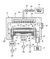
図1に、本発明の第1の実施形態によるプラズマエッチング装置の構成を示す。このプラズマエッチング装置は、下部2周波重畳印加方式の容量結合型プラズマエッチング装置として構成されており、たとえばアルミニウムまたはステンレス鋼からなる金属製の円筒型チャンバ(処理容器)10を有している。チャンバ10は保安接地されている。 FIG. 1 shows the configuration of a plasma etching apparatus according to the first embodiment of the present invention. This plasma etching apparatus is configured as a capacitive coupling type plasma etching apparatus of a lower two-frequency superimposing application method, and has a cylindrical chamber (processing vessel) 10 made of metal made of, for example, aluminum or stainless steel. The
チャンバ10の底面には、たとえばセラミックからなる環状の絶縁部材12を介して下部電極と基板保持台を兼ねるサセプタ14が設けられる。このサセプタ14は、本発明における第1および第2の下部電極をそれぞれ構成する上部サセプタ電極16および下部サセプタ電極18を有している。 A
上記環状絶縁部材12の上に環状または円筒状の給電体20が配置され、この円筒給電体20の上部に上部サセプタ電極16が略水平に取り付けられる。この上部サセプタ電極16は、被処理基板たとえば半導体ウエハWより一回り大きな口径を有する円形の平板電極であり、後述する理由から好ましくは抵抗率の高い導電材料たとえばタングステン(W)あるいはシリコン(Si)などで構成されている。給電体20は、伝送損失の少ない低抵抗率の材質たとえばアルミニウムからなる。
An annular or cylindrical
上部サセプタ電極16には、第1高周波電源22が整合器24、給電棒26および円筒給電体20を介して電気的に接続されている。第1高周波電源22は、サセプタ14上に保持される半導体ウエハWに対するイオンの引き込みに主として寄与する所定の周波数たとえば2MHzの第1高周波を所望のパワーで出力する。この第1高周波電源22からの第1高周波(2MHz)は、整合器24、給電棒26および円筒給電体20を通って上部サセプタ電極16に供給される。そして、上部サセプタ電極16の主面(上面)より上方のプラズマ空間PSに向けて放出されるようになっている。 A first high
下部サセプタ電極18は、抵抗率の低い導電材料たとえばアルミニウムからなる円形の略平板電極である。周囲(16,20)から電気的に絶縁された状態で環状絶縁部材12の内側かつ上部サセプタ電極16の直下に配置される。図示のように、下部サセプタ電極18の主面(上面)には電極中心が底になるようなテーパ状の凹部が形成され、この凹部に誘電体28が埋め込まれている。かかる電極構造は、電極径方向における電界強度ないしプラズマ密度の均一性を向上させるためのものであり、上記特許文献1(特開2004−363552)記載の技術を用いている。下部サセプタ電極18と環状絶縁部材12、上部サセプタ電極16との間の隙間は、放電を防止するために、たとえばセラミックからなる筒状絶縁体30および円板形絶縁体32で塞いでおくのが好ましい。 The
下部サセプタ電極18には、第2高周波電源34が整合器36および給電棒38を介して電気的に接続されている。第2高周波電源34は、プラズマの生成に主として寄与する所定の周波数たとえば40MHzの高周波を所望のパワーで出力する。この第2高周波電源34からの第2高周波(40MHz)は、整合器36および給電棒38を通って下部サセプタ電極18に供給される。そして、下部サセプタ電極18の主面(上面)より上方のプラズマ空間PSに向けて放出されるようになっている。 A second high
上部サセプタ電極16の上面には、半導体ウエハWを静電吸着力で保持するための静電チャック40が設けられている。この静電チャック40は導電膜からなる電極42を一対の絶縁層または絶縁シート44の間に挟み込んだものであり、電極42には直流電源46が電気的に接続されている。直流電源46からの直流電圧により、クーロン力で半導体ウエハWをチャック上に吸着保持できるようになっている。静電チャック40の周囲には、エッチングの均一性を向上させるためのたとえばシリコンからなるフォーカスリング48が配置されている。環状絶縁部材12および円筒状給電体20の外周面にはたとえば石英からなる円筒状の内壁部材50が貼り付けられている。 An
サセプタ14に載置される半導体ウエハWの温度を制御するために、上部サセプタ電極16の内部に冷媒室または冷媒通路(図示せず)を設け、外付けのチラーユニット(図示せず)より該冷媒通路に所定温度の冷媒たとえば冷却水を循環供給する構成も可能である。また、同じく半導体ウエハWの温度を制御するために、伝熱ガス供給機構(図示せず)からの伝熱ガスたとえばHeガスをガス供給ライン(図示せず)を介して静電チャック40の上面と半導体ウエハWの裏面との間に供給する構成も可能である。 In order to control the temperature of the semiconductor wafer W placed on the
チャンバ10の天井には、サセプタ12と平行に向かい合って接地電位の上部電極を兼ねるシャワーヘッド52が設けられている。このシャワーヘッド52は、多数のガス通気孔54aを有する下面の電極板54と、この電極板54を着脱可能に支持する電極支持体56とを有する。電極板54はたとえばSi,SiCからなり、電極支持体56はたとえばアルマイト処理されたアルミニウムからなる。電極支持体56の内部にガス室58が設けられ、このガス室58にはガス供給管60を介して処理ガス供給源62が接続されており、ガス供給管60にマスフローコントローラ(MFC)64および開閉バルブ66が設けられている。処理ガス供給源62より所定の処理ガスがガス室58に導入されると、電極板54のガス噴出孔54aよりサセプタ14上の半導体ウエハWに向けて処理ガスがシャワー状に噴出されるようになっている。 On the ceiling of the
サセプタ14とチャンバ10の側壁との間に形成される環状の空間は排気空間となっており、この排気空間の底にはチャンバ10の排気口68が設けられている。この排気口68に排気管70を介して排気装置72が接続されている。排気装置72は、ターボ分子ポンプなどの真空ポンプを有しており、チャンバ10の室内、特にプラズマ処理空間を所望の真空度まで減圧できるようになっている。また、チャンバ10の側壁には半導体ウエハWの搬入出口74を開閉するゲートバルブ76が取り付けられている。 An annular space formed between the susceptor 14 and the side wall of the
このプラズマエッチング装置において、エッチングを行なうには、先ずゲートバルブ76を開状態にして加工対象の半導体ウエハWをチャンバ10内に搬入して、静電チャック40の上に載置する。そして、処理ガス供給源62より所定の処理ガスつまりエッチングガス(一般に混合ガス)を所定の流量および流量比でチャンバ10内に導入し、排気装置72による真空排気でチャンバ10内の圧力を設定値にする。さらに、第1高周波電源22よりそれぞれ所定のパワーで第1高周波(2MHz)を上部サセプタ電極16に印加すると同時に、第2高周波電源34よりそれぞれ所定のパワーで第2高周波(40MHz)を下部サセプタ電極18に印加する。また、直流電源46より直流電圧を静電チャック40の電極42に印加して、半導体ウエハWを静電チャック40上に固定する。上部電極またはシャワーヘッド52より吐出されたエッチングガスは処理空間PSで高周波の放電によってプラズマ化し、このプラズマで生成されるラジカルやイオンによって半導体ウエハWの主面の膜がエッチングされる。 In order to perform etching in this plasma etching apparatus, first, the
この容量結合型プラズマエッチング装置は、サセプタ14の下部サセプタ電極18に40MHzというプラズマ生成に適した比較的高い周波数の第2高周波を印加することにより、プラズマを好ましい解離状態で高密度化し、より低圧の条件下でも高密度プラズマを形成することができる。それと同時に、サセプタ14の上部サセプタ電極16に2MHzというイオン引き込みに適した比較的低い周波数の第1高周波を印加することにより、サセプタ14の上方の半導体ウエハWに対して選択性の高い異方性のエッチングを施すことができる。 In this capacitively coupled plasma etching apparatus, by applying a second high frequency of a relatively high frequency suitable for plasma generation of 40 MHz to the
次に、この実施形態のプラズマエッチング装置において本発明の特徴部分であるサセプタ14の作用を詳細に説明する。 Next, the operation of the
上記したように、サセプタ14は上部サセプタ電極16と下部サセプタ電極18とに上下に2分割されており、上部サセプタ電極16には第1高周波電源22からの第1高周波(2MHz)が印加され、下部サセプタ電極18には第2高周波電源34からの第2高周波(40MHz)が印加される。 As described above, the
ここで、上部サセプタ電極16は単一材質かつ一定板厚の平板電極である。周波数の低い第1高周波(2MHz)の電流が上部サセプタ電極16の主面を流れる際の表面厚さは厚く(表皮効果は小さく)、電極中心部に偏ることなく電極主面の各位置からほぼ均一にプラズマ空間PSへ放出される。これにより、第1高周波(2MHz)によってサセプタ14上に形成される高周波電界の強度分布を電極半径方向においてほぼ均一化することができる。よって、該高周波電界に追従して半導体ウエハWに入射するイオンの引き込み量をウエハ面内の各部で均一化させ、ひいては異方性エッチングの形状または選択性の面内均一性を向上させることができる。 Here, the
一方、下部サセプタ電極18は、上記のように電極主面(上面)にテーパ状の凹部を形成し、この凹部に誘電体28を埋め込んでいる。周波数が相当高くて表皮厚さの薄い(表皮効果の大きい)第2高周波(40MHz)の電流に対しては電極中心への集中を抑制する作用が効いて、電極主面の各位置からほぼ均一にプラズマ空間PSへ放出させる。これにより、第2高周波(40MHz)によってサセプタ14上に形成される高周波電界の強度分布を電極半径方向においてほぼ均一化することができる。よって、高周波電界による加速でプラズマ空間PS内のガス分子に衝突する高周波電流または電子電流の大きさひいてはプラズマの密度をウエハ直上で均一化させ、ひいてはエッチングレートの面内均一性を向上させることができる。 On the other hand, the
なお、下部サセプタ電極18からプラズマ空間PSに向って高周波電流が放出されるに際して、上部サセプタ電極16にうず電流が流れ、このうず電流によって生成される磁界が下部サセプタ電極18からの高周波の直進を妨げるように働く。このことから、この実施形態では、上部サセプタ電極16を抵抗率の高い材質で構成することで、うず電流を抑制し、下部サセプタ電極18からプラズマ空間PSに向って放出される高周波が上部サセプタ電極16で受ける影響を少なくしている。 When a high-frequency current is emitted from the
以上、本発明の好適な実施形態について説明したが、上述した実施形態は本発明を限定するものではない。当業者にあっては、具体的な実施態様において本発明の技術思想および技術範囲から逸脱せずに種々の変形・変更を加えることが可能である。 As mentioned above, although preferred embodiment of this invention was described, embodiment mentioned above does not limit this invention. Those skilled in the art can make various modifications and changes in specific embodiments without departing from the technical idea and technical scope of the present invention.
たとえば、上記した実施形態における下部サセプタ電極18の電極構造は一例にすぎない。下部サセプタ電極18においては、電極径方向における電界強度ないしプラズマ密度の均一性を向上させるためにたとえば上記特許文献1に開示されるような種々の電極構造を採ることが可能であり、特に本発明においては上部サセプタ電極16から独立しているので、一層自由な電極構造を採ることが可能である。 For example, the electrode structure of the
たとえば、図2に示すように、下部サセプタ電極18をリング状に形成し、下部サセプタ電極18よりプラズマ空間PSに向って放出させる第2高周波を電極中心部で相対的かつ積極的に弱める構成とすることも可能である。また、下部サセプタ電極18をこのようにリング状に形成することで、上部サセプタ電極16に接続する給電棒26を下部サセプタ電極18の中心開口に通すこともできる。この場合、給電棒26と下部サセプタ電極18の内周面との間の隙間を円筒状の絶縁体78で塞いでよい。 For example, as shown in FIG. 2, the
また、本発明は上部電極側に高周波を印加する方式にも適用可能である。たとえば、図3に示す変形例は、上部電極80およびサセプタ(下部電極)82に周波数の異なる高周波をそれぞれ印加する方式の容量結合型プラズマエッチング装置において、上部電極80に本発明を応用したものである。この上部電極80は、プラズマ空間PSを挟んで直下のサセプタ82と対向する第1上部電極84と、この第1上部電極84の背後または上方に配置されている第2上部電極86とを有している。 The present invention can also be applied to a method of applying a high frequency to the upper electrode side. For example, the modification shown in FIG. 3 is an application of the present invention to the
より詳細には、第1上部電極84は、シャワーヘッドを兼ねた電極構造を有しており、リング状の誘電体88によってチャンバ90から電気的に絶縁された状態つまりフローティング状態で取り付けられている。この第1上部電極84には可変直流電源92より直流電圧が印加される。また、第1上部電極84の内部またはガス室にはガス供給管60を介して処理ガス供給源62が接続される。 More specifically, the first
第2上部電極86は、上記実施形態における下部サセプタ電極18と同様の電極構造を有するものでよく、逆さの向きで(下方を向いて)配置される。また、周囲を絶縁体94で囲まれており、第1上部電極84やチャンバ90から電気的に絶縁されている。この第2上部電極86には高周波電源96より整合器(図示せず)を介してプラズマ生成用の高周波(たとえば60MHz)が印加される。 The second
サセプタ82は、通常の円板形に形成され、その上面に半導体ウエハWを保持する電極構造を有しており、高周波電源98より整合器(図示せず)を介してイオン引き込み用の高周波(たとえば13.56MHz)を印加される。 The
このプラズマエッチング装置においては、第2上部電極86よりプラズマ空間PSに向けて放出される高周波(60MHz)によって電極半径方向において均一化されたプラズマを生成することができる。また、プラズマ生成用の高周波(60MHz)から独立してサセプタ82よりプラズマ空間PSに向けて放出される高周波(13.56MHz)によって電極半径方向においてほぼ均一に半導体ウエハWにイオンを引き込むことができる。 In this plasma etching apparatus, plasma made uniform in the electrode radial direction can be generated by the high frequency (60 MHz) emitted from the second
第1上部電極86は、上記した実施形態と同様に、たとえばタングステンやシリコンなどの高抵抗率の材質からなり、第2上部電極86からプラズマ空間PSに向う高周波(60MHz)を妨害しないようにしてよい。また、直流電源92より印加される直流電圧により、たとえばプラズマに種々の作用(たとえばプラズマポテンシャルを制御する作用、プラズマ密度を上昇させる作用)を加えることができる。 The first
本発明は、上記実施形態のようなプラズマエッチングに限定されず、プラズマCVD、プラズマ酸化、プラズマ窒化、スパッタリングなどの他のプラズマ処理にも適用可能である。また、本発明における被処理基板は半導体ウエハに限るものではなく、フラットパネルディスプレイ用の基板や、フォトマスク、CD基板、プリント基板等も可能である。 The present invention is not limited to plasma etching as in the above embodiment, but can be applied to other plasma processes such as plasma CVD, plasma oxidation, plasma nitridation, and sputtering. In addition, the substrate to be processed in the present invention is not limited to a semiconductor wafer, and a flat panel display substrate, a photomask, a CD substrate, a printed substrate, and the like are also possible.
10 チャンバ
14 サセプタ
16 上部サセプタ電極
18 下部サセプタ電極
22 第1高周波電源
30,32 絶縁体
34 第2高周波電源
52 上部電極(シャワーヘッド)
62 処理ガス供給源
80 上部電極
82 サセプタ
84 第1上部電極
86 第2上部電極
90 チャンバ
92 可変直流電源
96,98 高周波電源10
22 First high
62 Processing
Claims (11)
Translated fromJapanese前記処理容器内で被処理基板を支持する第1の下部電極と、
前記第1の下部電極と対向してその上方に配置される上部電極と、
前記第1の下部電極から電気的に絶縁された状態でその下に配置される第2の下部電極と、
前記上部電極と前記第1の下部電極との間の空間に所望の処理ガスを供給する処理ガス供給部と、
前記第1の下部電極に第1の周波数を有する第1の高周波を印加する第1の高周波給電部と、
前記第2の下部電極に前記第1の周波数よりも高い第2の周波数を有する第2の高周波を印加する第2の高周波給電部と
を有するプラズマ処理装置。A processing container capable of being evacuated;
A first lower electrode for supporting a substrate to be processed in the processing container;
An upper electrode disposed above and opposite the first lower electrode;
A second lower electrode disposed below the first lower electrode in a state of being electrically insulated from the first lower electrode;
A processing gas supply unit that supplies a desired processing gas to a space between the upper electrode and the first lower electrode;
A first high-frequency power feeding unit that applies a first high-frequency wave having a first frequency to the first lower electrode;
A plasma processing apparatus, comprising: a second high-frequency power supply unit that applies a second high frequency signal having a second frequency higher than the first frequency to the second lower electrode.
前記第2の高周波給電部は、前記第2の下部電極に接続される第2の給電棒を有する、The second high-frequency power supply unit has a second power supply rod connected to the second lower electrode,
請求項6に記載のプラズマ処理装置。The plasma processing apparatus according to claim 6.
Priority Applications (3)
| Application Number | Priority Date | Filing Date | Title |
|---|---|---|---|
| JP2006091406AJP4753306B2 (en) | 2006-03-29 | 2006-03-29 | Plasma processing equipment |
| US11/692,363US8157953B2 (en) | 2006-03-29 | 2007-03-28 | Plasma processing apparatus |
| US13/419,116US8529730B2 (en) | 2006-03-29 | 2012-03-13 | Plasma processing apparatus |
Applications Claiming Priority (1)
| Application Number | Priority Date | Filing Date | Title |
|---|---|---|---|
| JP2006091406AJP4753306B2 (en) | 2006-03-29 | 2006-03-29 | Plasma processing equipment |
Related Child Applications (1)
| Application Number | Title | Priority Date | Filing Date |
|---|---|---|---|
| JP2011065636ADivisionJP5367000B2 (en) | 2011-03-24 | 2011-03-24 | Plasma processing equipment |
Publications (2)
| Publication Number | Publication Date |
|---|---|
| JP2007266436A JP2007266436A (en) | 2007-10-11 |
| JP4753306B2true JP4753306B2 (en) | 2011-08-24 |
Family
ID=38639109
Family Applications (1)
| Application Number | Title | Priority Date | Filing Date |
|---|---|---|---|
| JP2006091406AActiveJP4753306B2 (en) | 2006-03-29 | 2006-03-29 | Plasma processing equipment |
Country Status (1)
| Country | Link |
|---|---|
| JP (1) | JP4753306B2 (en) |
Families Citing this family (5)
| Publication number | Priority date | Publication date | Assignee | Title |
|---|---|---|---|---|
| JP5223377B2 (en) | 2008-02-29 | 2013-06-26 | 東京エレクトロン株式会社 | Electrode for plasma processing apparatus, plasma processing apparatus and plasma processing method |
| JP5264231B2 (en)* | 2008-03-21 | 2013-08-14 | 東京エレクトロン株式会社 | Plasma processing equipment |
| US9449795B2 (en)* | 2013-02-28 | 2016-09-20 | Novellus Systems, Inc. | Ceramic showerhead with embedded RF electrode for capacitively coupled plasma reactor |
| US10373804B2 (en)* | 2017-02-03 | 2019-08-06 | Applied Materials, Inc. | System for tunable workpiece biasing in a plasma reactor |
| KR102311213B1 (en)* | 2019-04-19 | 2021-10-13 | 세메스 주식회사 | Apparatus and method for treating a substrate |
Family Cites Families (8)
| Publication number | Priority date | Publication date | Assignee | Title |
|---|---|---|---|---|
| JP2651597B2 (en)* | 1988-06-27 | 1997-09-10 | 富士通株式会社 | Dry etching method and apparatus |
| JPH1197430A (en)* | 1997-07-14 | 1999-04-09 | Applied Materials Inc | High density plasma process chamber |
| JP2004531880A (en)* | 2001-03-13 | 2004-10-14 | アプライド マテリアルズ インコーポレイテッド | Substrate support with dual electrodes |
| JP2002313737A (en)* | 2001-04-13 | 2002-10-25 | Tdk Corp | Plasma treating equipment |
| JP4137419B2 (en)* | 2001-09-28 | 2008-08-20 | 東京エレクトロン株式会社 | Plasma processing equipment |
| JP4472372B2 (en)* | 2003-02-03 | 2010-06-02 | 株式会社オクテック | Plasma processing apparatus and electrode plate for plasma processing apparatus |
| US20050130620A1 (en)* | 2003-12-16 | 2005-06-16 | Andreas Fischer | Segmented radio frequency electrode apparatus and method for uniformity control |
| JP4515755B2 (en)* | 2003-12-24 | 2010-08-04 | 東京エレクトロン株式会社 | Processing equipment |
- 2006
- 2006-03-29JPJP2006091406Apatent/JP4753306B2/enactiveActive
Also Published As
| Publication number | Publication date |
|---|---|
| JP2007266436A (en) | 2007-10-11 |
Similar Documents
| Publication | Publication Date | Title |
|---|---|---|
| JP5317424B2 (en) | Plasma processing equipment | |
| JP4472372B2 (en) | Plasma processing apparatus and electrode plate for plasma processing apparatus | |
| JP5264231B2 (en) | Plasma processing equipment | |
| JP5064707B2 (en) | Plasma processing equipment | |
| KR100652982B1 (en) | Plasma processing method and apparatus | |
| JP5348848B2 (en) | Plasma processing equipment | |
| US8529730B2 (en) | Plasma processing apparatus | |
| JP2009123934A (en) | Plasma treatment apparatus | |
| JP2007005491A (en) | Electrode assembly and plasma processing apparatus | |
| KR101898079B1 (en) | Plasma processing apparatus | |
| JP2009123929A (en) | Plasma treatment apparatus | |
| CN100495654C (en) | Plasma processing device, electrode plate for plasma processing device, and electrode plate manufacturing method | |
| WO2019239893A1 (en) | Mounting stage, substrate processing device, and edge ring | |
| JP2010135813A (en) | Plasma processing apparatus and electrode plate therefor | |
| KR20170132096A (en) | Plasma processing method | |
| JP4753306B2 (en) | Plasma processing equipment | |
| US8342121B2 (en) | Plasma processing apparatus | |
| JP5367000B2 (en) | Plasma processing equipment | |
| JP7333712B2 (en) | Electrostatic chuck, support table and plasma processing equipment | |
| KR20140051280A (en) | Plasma processing device | |
| JP5264238B2 (en) | Plasma processing equipment | |
| JP5064708B2 (en) | Plasma processing equipment | |
| JP2021097065A (en) | Ring assembly, board support, and board processing device |
Legal Events
| Date | Code | Title | Description |
|---|---|---|---|
| A621 | Written request for application examination | Free format text:JAPANESE INTERMEDIATE CODE: A621 Effective date:20090205 | |
| A977 | Report on retrieval | Free format text:JAPANESE INTERMEDIATE CODE: A971007 Effective date:20101224 | |
| A131 | Notification of reasons for refusal | Free format text:JAPANESE INTERMEDIATE CODE: A131 Effective date:20110125 | |
| A521 | Request for written amendment filed | Free format text:JAPANESE INTERMEDIATE CODE: A523 Effective date:20110324 | |
| TRDD | Decision of grant or rejection written | ||
| A01 | Written decision to grant a patent or to grant a registration (utility model) | Free format text:JAPANESE INTERMEDIATE CODE: A01 Effective date:20110517 | |
| A01 | Written decision to grant a patent or to grant a registration (utility model) | Free format text:JAPANESE INTERMEDIATE CODE: A01 | |
| A61 | First payment of annual fees (during grant procedure) | Free format text:JAPANESE INTERMEDIATE CODE: A61 Effective date:20110519 | |
| FPAY | Renewal fee payment (event date is renewal date of database) | Free format text:PAYMENT UNTIL: 20140603 Year of fee payment:3 | |
| R150 | Certificate of patent or registration of utility model | Ref document number:4753306 Country of ref document:JP Free format text:JAPANESE INTERMEDIATE CODE: R150 Free format text:JAPANESE INTERMEDIATE CODE: R150 | |
| R250 | Receipt of annual fees | Free format text:JAPANESE INTERMEDIATE CODE: R250 | |
| R250 | Receipt of annual fees | Free format text:JAPANESE INTERMEDIATE CODE: R250 | |
| R250 | Receipt of annual fees | Free format text:JAPANESE INTERMEDIATE CODE: R250 | |
| R250 | Receipt of annual fees | Free format text:JAPANESE INTERMEDIATE CODE: R250 | |
| R250 | Receipt of annual fees | Free format text:JAPANESE INTERMEDIATE CODE: R250 | |
| R250 | Receipt of annual fees | Free format text:JAPANESE INTERMEDIATE CODE: R250 | |
| R250 | Receipt of annual fees | Free format text:JAPANESE INTERMEDIATE CODE: R250 |