JP4748641B2 - Information processing system - Google Patents
Information processing systemDownload PDFInfo
- Publication number
- JP4748641B2 JP4748641B2JP2004352928AJP2004352928AJP4748641B2JP 4748641 B2JP4748641 B2JP 4748641B2JP 2004352928 AJP2004352928 AJP 2004352928AJP 2004352928 AJP2004352928 AJP 2004352928AJP 4748641 B2JP4748641 B2JP 4748641B2
- Authority
- JP
- Japan
- Prior art keywords
- latency
- access
- memory
- memory control
- request
- Prior art date
- Legal status (The legal status is an assumption and is not a legal conclusion. Google has not performed a legal analysis and makes no representation as to the accuracy of the status listed.)
- Expired - Fee Related
Links
Images


Classifications
- G—PHYSICS
- G06—COMPUTING OR CALCULATING; COUNTING
- G06F—ELECTRIC DIGITAL DATA PROCESSING
- G06F5/00—Methods or arrangements for data conversion without changing the order or content of the data handled
- G06F5/06—Methods or arrangements for data conversion without changing the order or content of the data handled for changing the speed of data flow, i.e. speed regularising or timing, e.g. delay lines, FIFO buffers; over- or underrun control therefor
- G06F5/10—Methods or arrangements for data conversion without changing the order or content of the data handled for changing the speed of data flow, i.e. speed regularising or timing, e.g. delay lines, FIFO buffers; over- or underrun control therefor having a sequence of storage locations each being individually accessible for both enqueue and dequeue operations, e.g. using random access memory
- G06F5/12—Means for monitoring the fill level; Means for resolving contention, i.e. conflicts between simultaneous enqueue and dequeue operations
- G—PHYSICS
- G06—COMPUTING OR CALCULATING; COUNTING
- G06F—ELECTRIC DIGITAL DATA PROCESSING
- G06F13/00—Interconnection of, or transfer of information or other signals between, memories, input/output devices or central processing units
- G06F13/14—Handling requests for interconnection or transfer
- G06F13/16—Handling requests for interconnection or transfer for access to memory bus
- G06F13/1605—Handling requests for interconnection or transfer for access to memory bus based on arbitration
- G06F13/1652—Handling requests for interconnection or transfer for access to memory bus based on arbitration in a multiprocessor architecture
- G06F13/1663—Access to shared memory
- G—PHYSICS
- G06—COMPUTING OR CALCULATING; COUNTING
- G06F—ELECTRIC DIGITAL DATA PROCESSING
- G06F13/00—Interconnection of, or transfer of information or other signals between, memories, input/output devices or central processing units
- G06F13/14—Handling requests for interconnection or transfer
- G06F13/16—Handling requests for interconnection or transfer for access to memory bus
- G06F13/1668—Details of memory controller
- G06F13/1673—Details of memory controller using buffers
Landscapes
- Engineering & Computer Science (AREA)
- Theoretical Computer Science (AREA)
- Physics & Mathematics (AREA)
- General Engineering & Computer Science (AREA)
- General Physics & Mathematics (AREA)
- Memory System (AREA)
- Image Input (AREA)
Description
Translated fromJapanese本発明は、情報の処理を可能とする情報処理システムに関し、例えば画像データを取り扱う装置に適用して有効な技術に関する。 The present invention relates to an information processing system that can process information, and relates to a technique that is effective when applied to an apparatus that handles image data, for example.
従来のメモリ制御方法としては、例えば、CPU(中央演算回路)とそれ以外のメモリをアクセスする複数のマスタとメモリから構成される情報処理装置では、各マスタからのメモリアクセス要求が競合した場合、これらメモリアクセス要求の優先順位に従って、処理を行っている。このようなメモリ制御方法としては、メモリをアクセスするマスタであるホストコンピュータ側の制御回路と、ハードディスク装置側の制御回路FIFOメモリのデータがオーバーフローやアンダーフローしない程度に、DRAMをアクセスするためのアクセス権を切り替えてデータ転送を行う技術が知られている(例えば特許文献1参照)。 As a conventional memory control method, for example, in an information processing apparatus composed of a plurality of masters and memories that access a CPU (central processing circuit) and other memories, when memory access requests from each master compete, Processing is performed in accordance with the priority order of these memory access requests. As such a memory control method, there is an access for accessing the DRAM to such an extent that the data in the control circuit on the host computer which is the master accessing the memory and the control circuit FIFO memory on the hard disk device side do not overflow or underflow. A technique for transferring data by switching rights is known (see, for example, Patent Document 1).
また、メモリをアクセスするマスタであるCPUと液晶表示装置及びCRT表示装置と、メモリから構成される情報処理装置のメモリ制御方法で、液晶表示用及びCRT表示装置が装備しているFIFOメモリのデータがオーバーフローやアンダーフローしない程度に、CPUからDRAMへのアクセスを優先させ、データ転送を行う技術が知られている(例えば特許文献2参照)。 In addition, a memory control method for an information processing device including a CPU, a liquid crystal display device, a CRT display device, and a memory as a master for accessing the memory, and data in the FIFO memory provided for the liquid crystal display and the CRT display device. Is known to transfer data by giving priority to access from the CPU to the DRAM to such an extent that overflow or underflow does not occur (see, for example, Patent Document 2).
さらにメモリをアクセスするマスタであるCPUとDMA装置と、メモリから構成される情報処理装置のメモリ制御方法で、DMA装置が装備しているFIFOメモリのデータがオーバーフローやアンダーフローしない程度に、CPUからDRAMへのアクセスを優先させ、データ転送を行う技術が知られている(特許文献3参照)記載される。 Furthermore, in the memory control method of the information processing device composed of the CPU and DMA device that are the masters accessing the memory, the data from the FIFO memory provided in the DMA device is not overflowed or underflowed from the CPU. A technique for transferring data by prioritizing access to a DRAM is known (see Patent Document 3).
本願発明者は、以下のような動画像録画や再生、グラフィックス処理を実現する制御技術について以下のような検討を行った。 The inventor of the present application has made the following studies on the control technology for realizing the following moving image recording, reproduction, and graphics processing.
動画像の録画では、撮像装置で撮像した動画像を、デジタルデータへ変換して、いったんメモリ装置へ取り込む。その次に、メモリへ取り込まれた動画像データは、すぐに表示装置へ転送され、動画像が表示される。これらの処理と同時に、取り込まれた動画像データを読み出して圧縮処理を行い、圧縮データを再度メモリへ書き込む。 In recording a moving image, the moving image picked up by the image pickup device is converted into digital data and once taken into the memory device. Next, the moving image data taken into the memory is immediately transferred to the display device, and the moving image is displayed. Simultaneously with these processes, the captured moving image data is read and subjected to a compression process, and the compressed data is written into the memory again.
再生する場合は、メモリへ格納している圧縮データを読み出し、伸張処理を行い、再度メモリへ書き込む。その後、伸張されたデータを読み出し、表示装置へ転送し、動画像を表示する。 When reproducing, the compressed data stored in the memory is read out, decompressed, and written again into the memory. Thereafter, the decompressed data is read out, transferred to the display device, and a moving image is displayed.
このように、動画像の録画や再生においては、撮像、表示、及び圧縮や伸張処理は、同時に実行され、さらに1秒間に30画面分の処理を行う必要がある。つまり、1画面分の処理を30分の1秒以内に終了させなければならない。 As described above, in recording and playback of moving images, imaging, display, compression, and decompression processing are performed simultaneously, and it is necessary to perform processing for 30 screens per second. That is, processing for one screen must be completed within 1/30 second.
グラフィックス処理では、ジオメトリ処理が行われ、その後レンダリング処理が行われる。 In the graphics processing, geometry processing is performed, and then rendering processing is performed.
ジオメトリ処理は、3次元図形を表すため、図形の座標計算を行うことである。レンダリング処理は、画像表示装置へ表示するために、ジオメトリ処理後の図形に、色、明るさ、奥行き、絵柄といった視覚的効果を付け足す処理である。画像はメモリへ格納されており、現在の画像を読み出して、ジオメトリ処理が行われ、その後、レンダリング処理が行われ、新しい画像が生成され、再度メモリへ格納される。 Geometry processing is to perform coordinate calculation of a figure to represent a three-dimensional figure. The rendering process is a process for adding visual effects such as color, brightness, depth, and design to the figure after the geometry process for display on the image display device. The image is stored in the memory, the current image is read out, geometry processing is performed, then rendering processing is performed, a new image is generated, and stored again in the memory.
最後に、メモリへ格納された画像は画像表示装置に表示される。 Finally, the image stored in the memory is displayed on the image display device.
このようなグラフィックス処理では、ジオメトリ処理、レンダリング処理及び表示は同時に処理され、加えて1秒間に30画面分のグラフィックス処理を行う必要がある。つまり、1画面分のグラフィックス処理を30分の1秒以内に終了させなければならない。 In such graphics processing, geometry processing, rendering processing, and display are processed simultaneously, and in addition, it is necessary to perform graphics processing for 30 screens per second. That is, the graphics processing for one screen must be completed within 1/30 second.
しかし、上記従来技術では、マスタ側の処理を一定時間以内に終了させることを保障することができないので、場合によっては圧縮処理が滞り、録画データに欠落が生じたり、表示画面が乱れたり、情報処理システムの動作品質を低下させてしまうおそれがある。 However, in the above prior art, it is not possible to guarantee that the processing on the master side will be completed within a certain time, so in some cases the compression process is delayed, the recorded data is lost, the display screen is disturbed, the information There is a possibility that the operation quality of the processing system may be degraded.
本発明の目的は、メモリ装置をアクセスする複数のマスタに対して、必要なデータを円滑に転送するための技術を提供することにある。 An object of the present invention is to provide a technique for smoothly transferring necessary data to a plurality of masters accessing a memory device.
また、本発明の別の目的は、バスマスタにおける処理の効率化を図るための技術を提供することにある。 Another object of the present invention is to provide a technique for improving the efficiency of processing in a bus master.
本発明の上記並びにその他の目的と新規な特徴は本明細書の記述及び添付図面から明らかになるであろう。 The above and other objects and novel features of the present invention will be apparent from the description of this specification and the accompanying drawings.
本願において開示される発明のうち代表的なものの概要を簡単に説明すれば下記の通りである。 The following is a brief description of an outline of typical inventions disclosed in the present application.
すなわち、メモリ装置と、上記メモリ装置の動作を制御可能なメモリ制御装置と、それぞれ上記メモリ制御装置を介して上記メモリ装置へアクセス可能な複数のバスマスタと、を含む情報処理システムにおいて、上記メモリ装置からのデータ転送をいつまでに開始できるかという時間情報を、アクセス要求にかかる上記バスマスタに通知可能な制御回路を上記メモリ制御装置内に設ける。 That is, in an information processing system including a memory device, a memory control device capable of controlling the operation of the memory device, and a plurality of bus masters each capable of accessing the memory device via the memory control device, the memory device A control circuit is provided in the memory control device that can notify the bus master of the access request about the time information on when the data transfer from can be started.
上記の手段によれば、上記メモリ装置からのデータ転送をいつまでに開始できるかという時間情報が、アクセス要求にかかるバスマスタに通知される。バスマスタは、通知された時間情報を上記メモリ装置へのアクセス要求発するか否かの判断材料とすることができ、それによって各バスマスタは無駄なアクセス要求の発生を回避することができる。このことが、メモリ装置をアクセスする複数のマスタに対するデータ転送の円滑化を達成する。また、上記メモリ装置からのデータ転送をいつまでに開始できるかという時間情報が、アクセス要求にかかるバスマスタに通知されることにより、各バスマスタは、内部処理を柔軟に調整することができ、このことが、バスマスタ内の処理の効率化を達成する。 According to the above means, the time information indicating when the data transfer from the memory device can be started is notified to the bus master concerning the access request. The bus master can use the notified time information to determine whether or not to issue an access request to the memory device, whereby each bus master can avoid the generation of useless access requests. This achieves smooth data transfer to a plurality of masters accessing the memory device. In addition, the time information indicating when the data transfer from the memory device can be started before is notified to the bus master related to the access request, so that each bus master can flexibly adjust the internal processing. , Achieve more efficient processing in the bus master.
そして、メモリ装置と、上記メモリ装置の動作を制御可能なメモリ制御装置と、それぞれ上記メモリ制御装置を介して上記メモリへアクセス可能な複数のバスマスタとを含む情報処理システムにおいて、上記バスマスタは、上記メモリアクセスにかかる要求データを受け取るまでの最大許容時間情報を上記メモリ制御装置に通知する機能を含む。 In an information processing system including a memory device, a memory control device capable of controlling the operation of the memory device, and a plurality of bus masters each capable of accessing the memory via the memory control device, the bus master is configured as described above. A function for notifying the memory control device of information on the maximum allowable time until the request data for memory access is received.
上記の手段によれば、上記メモリアクセスにかかる要求データを受け取るまでの最大許容時間情報が上記メモリ制御装置に通知されることから、上記メモリ制御装置では、通知された時間情報に基づいて優先順位の変更などが可能とされ、最大許容時間を逸脱したデータ転送を回避することができ、このことが、データ転送の円滑化を達成する。 According to the above means, since the maximum allowable time information until the request data related to the memory access is received is notified to the memory control device, the memory control device uses the priority order based on the notified time information. And the like, and data transfer outside the maximum allowable time can be avoided, which achieves smooth data transfer.
このとき、上記複数のバスマスタからのアクセス要求の競合の調停、及び上記複数のバスマスタから通知された上記最大許容時間情報の調停を行うアクセス調停装置を設けることができる。 At this time, it is possible to provide an access arbitration device that arbitrates contention of access requests from the plurality of bus masters and arbitrates the maximum allowable time information notified from the plurality of bus masters.
上記メモリ制御装置は、上記最大許容時間情報に基づいて上記メモリに対するアクセス順位を決定するように構成することができる。 The memory control device may be configured to determine an access order for the memory based on the maximum allowable time information.
さらに、上記メモリ制御装置は、上記バスマスタからのアクセス要求に対する上記メモリのアクセス状況に応じて上記アクセス順位を変更可能に構成することができる。 Further, the memory control device can be configured to change the access order according to the access status of the memory in response to an access request from the bus master.
メモリ制御装置は、上記バスマスタからのアクセス要求情報を保持可能なバッファと、時間情報を保存可能なレジスタとを備え、上記バッファに保持されているアクセス要求情報と、上記バッファに保持されているアクセス要求情報とに基づいて上記データ到達時間を計算するように構成することができる。 The memory control device includes a buffer capable of holding access request information from the bus master and a register capable of storing time information, the access request information held in the buffer, and the access held in the buffer The data arrival time can be calculated based on the request information.
また、メモリと、上記メモリの動作を制御可能なメモリ制御装置と、それぞれ上記メモリ制御装置を介して上記メモリへアクセス可能な複数のバスマスタとを含む情報処理システムにおいて、上記メモリ制御装置は、上記バスマスタからのアクセス要求を保持可能なバッファを含み、上記バッファの利用権を上記バスマスタ毎に設定可能に構成することができる。 Further, in an information processing system including a memory, a memory control device capable of controlling the operation of the memory, and a plurality of bus masters each capable of accessing the memory via the memory control device, the memory control device includes: A buffer that can hold an access request from the bus master is included, and the right to use the buffer can be set for each bus master.
上記バスマスタによる上記バッファの利用権を予約可能なフラグ回路を上記メモリ制御装置内に設けることができる。 A flag circuit capable of reserving the right to use the buffer by the bus master can be provided in the memory control device.
上記バスマスタには、上記フラグ設定回路に設定された上記バッファの利用権の予約を解除する機能を設けることができる。 The bus master can be provided with a function of canceling the reservation of the right to use the buffer set in the flag setting circuit.
上記複数のバスマスタと、上記メモリ制御装置とを一つの半導体チップに形成することができる。 The plurality of bus masters and the memory control device can be formed on one semiconductor chip.
上記複数のバスマスタと、上記メモリ制御装置と、上記メモリとを一つの半導体チップに形成することができる。 The plurality of bus masters, the memory control device, and the memory can be formed on one semiconductor chip.
上記複数のバスマスタと、上記メモリ制御装置とを第1半導体チップに形成し、上記メモリ装置を第2半導体チップに形成し、上記第1半導体チップと上記第2半導体チップとを共通の封止体によって封止することができる。 The plurality of bus masters and the memory control device are formed on a first semiconductor chip, the memory device is formed on a second semiconductor chip, and the first semiconductor chip and the second semiconductor chip are shared with each other. Can be sealed.
本願において開示される発明のうち代表的なものによって得られる効果を簡単に説明すれば下記の通りである。 The effects obtained by the representative ones of the inventions disclosed in the present application will be briefly described as follows.
すなわち、メモリ装置をアクセスする複数のマスタに対するデータ転送の円滑化を図ることができる。また、バスマスタ内の処理を柔軟に調整することができ、それによってバスマスタ内の処理の効率化を図ることができる。 That is, data transfer to a plurality of masters that access the memory device can be facilitated. In addition, the processing in the bus master can be flexibly adjusted, thereby increasing the efficiency of the processing in the bus master.
<実施の形態1>
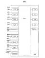
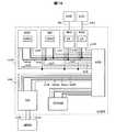
図1には、本願にかかる情報処理システムの構成例が示される。<
FIG. 1 shows a configuration example of an information processing system according to the present application.
図1に示される情報処理システムは、特に制限されないが、中央演算回路CPUを装備するマイクロコンピュータMS0、データ圧縮/伸張回路MACCを装備する画像処理装置MS1、データ入力装置MS2、データ出力装置MS3、アクセス調停装置ARB、内蔵メモリ装置OCRAM、メモリ制御装置SL0、撮像装置CCD、画像表示装置LCD、メモリ装置MEM0を含み、クロックCLKに同期して動作する。 The information processing system shown in FIG. 1 is not particularly limited, but includes a microcomputer MS0 equipped with a central processing circuit CPU, an image processing device MS1, a data input device MS2, a data output device MS3 equipped with a data compression / decompression circuit MACC, It includes an access arbitration device ARB, a built-in memory device OCRAM, a memory control device SL0, an imaging device CCD, an image display device LCD, and a memory device MEM0, and operates in synchronization with the clock CLK.
特に制限されないが、マイクロコンピュータMS0、画像処理装置MS1、データ入力装置MS2、データ出力装置MS3、アクセス調停装置ARB、メモリ制御装置SL0および内蔵メモリ装置OCRAMは、同一基板上に形成される。 Although not particularly limited, the microcomputer MS0, the image processing device MS1, the data input device MS2, the data output device MS3, the access arbitration device ARB, the memory control device SL0, and the built-in memory device OCRAM are formed on the same substrate.
特に制限されないが、メモリ装置MEM0および内蔵メモリ装置OCRAMはDRAM、SRAM及び不揮発性メモリで構成することが可能である。 マイクロコンピュータMS0は、例えば中央演算装置CPUと、アクセス要求のためのリクエストバッファrqm0と、アクセス要求に対する応答のためのレスポンスバッファrsm0から構成される。 Although not particularly limited, the memory device MEM0 and the built-in memory device OCRAM can be configured by DRAM, SRAM, and nonvolatile memory. The microcomputer MS0 includes, for example, a central processing unit CPU, a request buffer rqm0 for an access request, and a response buffer rsm0 for a response to the access request.
画像処理装置MS1は、データ圧縮/伸張装置MACCと、アクセス要求のためのリクエストバッファrqm1と、アクセス要求に対する応答のためのレスポンスバッファrsm1から構成される。 The image processing device MS1 includes a data compression / decompression device MACC, a request buffer rqm1 for an access request, and a response buffer rsm1 for a response to the access request.
データ入力装置MS2は、画像入力回路VIFと、アクセス要求のためのリクエストバッファrqm2と、アクセス要求に対する応答のためのレスポンスバッファrsm2を含んで成り、撮像装置CCDからの動画像データdinを取り込む。 The data input device MS2 includes an image input circuit VIF, a request buffer rqm2 for access request, and a response buffer rsm2 for response to the access request, and takes in the moving image data din from the imaging device CCD.
データ出力装置MS3は、画像出力装置LIFと、アクセス要求のためのリクエストバッファrqm3と、アクセス要求に対する応答のためのレスポンスバッファrsm3を含み、画像表示装置LCDに動画像データdoutを出力する。 The data output device MS3 includes an image output device LIF, a request buffer rqm3 for an access request, and a response buffer rsm3 for responding to the access request, and outputs moving image data dout to the image display device LCD.
メモリ制御装置SL0は、メモリ制御回路SDCONと、レジスタ回路sregと、アクセス要求のためのリクエストバッファreq0と、アクセス要求に対する応答のためのレスポンスバッファres0を含み、上記メモリ装置MEM0の動作を制御する。 The memory control device SL0 includes a memory control circuit SDCON, a register circuit sreg, a request buffer req0 for an access request, and a response buffer res0 for responding to the access request, and controls the operation of the memory device MEM0.
内蔵メモリ装置OCRAMは、メモリアレイRAMとメモリ制御回路SDCONと、レジスタ回路rregと、アクセス要求のためのリクエストバッファreg1と、アクセス要求に対する応答のためのレスポンスバッファres1を含んで構成される。 The built-in memory device OCRAM includes a memory array RAM, a memory control circuit SDCON, a register circuit rreg, a request buffer reg1 for an access request, and a response buffer res1 for responding to the access request.
上記マイクロコンピュータMS0と、画像処理装置MS1と、データ入力装置MS2と、データ出力装置MS3は、何れもバスマスタとされ、それぞれの固有のマスタ識別番号が設定されており、マイクロコンピュータMS0のマスタ識別番号midは「0」に、画像処理装置MS1のマスタ識別番号midは「1」に、データ入力装置MS2のマスタ識別番号midは「2」に、データ出力装置MS3のマスタ識別番号midは「3」に設定されている。 The microcomputer MS0, the image processing device MS1, the data input device MS2, and the data output device MS3 are all bus masters, and each has a unique master identification number. The master identification number of the microcomputer MS0 mid is “0”, the master identification number mid of the image processing apparatus MS1 is “1”, the master identification number mid of the data input apparatus MS2 is “2”, and the master identification number mid of the data output apparatus MS3 is “3”. Is set to
上記構成の動作を説明する。 The operation of the above configuration will be described.
先ず、画像を録画する場合の動作を簡単に説明する。 First, an operation for recording an image will be briefly described.
撮像装置CCDで撮像して得られた動画像データdinは、データ入力装置MS2によって取り込まれ、アクセス調停装置ARBと、メモリ制御装置SL0を介して、メモリ装置MEM0へ転送される。 The moving image data din obtained by imaging with the imaging device CCD is taken in by the data input device MS2, and transferred to the memory device MEM0 via the access arbitration device ARB and the memory control device SL0.
マイクロコンピュータMS0は、アクセス調停装置ARBと、メモリ制御装置SL0とを介してメモリ装置MEM0から動画データを読み出し、それに回転処理を施す。その処理結果はアクセス調停装置ARBと、メモリ制御装置SL0とを介して、再度、メモリ装置MEM0へ書き込まれる。 The microcomputer MS0 reads the moving image data from the memory device MEM0 via the access arbitration device ARB and the memory control device SL0, and performs rotation processing on it. The processing result is written again into the memory device MEM0 via the access arbitration device ARB and the memory control device SL0.
データ出力装置MS3は、メモリ装置MEM0からアクセス調停装置ARBと、メモリ制御装置SL0とを介して、マイクロコンピュータMS0によって回転処理が施された動画像データを読み出し、それを動画像表示のための画像表示装置LCDへ転送する。 The data output device MS3 reads out the moving image data rotated by the microcomputer MS0 from the memory device MEM0 via the access arbitration device ARB and the memory control device SL0, and outputs the image data for displaying the moving image. Transfer to display LCD.
画像処理装置MS1は、メモリ装置MEM0から、アクセス調停装置ARBと、メモリ制御装置SL0とを介して、マイクロコンピュータMS0によって回転処理が施された画像データを読み出し、データ圧縮を施す。その処理結果はアクセス調停装置ARBと、メモリ制御装置SL0とを介して、再度メモリ装置MEM0へ書き込まれる。 The image processing device MS1 reads out the image data that has been subjected to the rotation processing by the microcomputer MS0 from the memory device MEM0 via the access arbitration device ARB and the memory control device SL0, and performs data compression. The processing result is written to the memory device MEM0 again via the access arbitration device ARB and the memory control device SL0.
アクセス調停装置ARBとメモリ制御装置SL0は互いに連携し、上述した録画に必要な処理を一定の時間内に完了し、録画を滞りなく実行するために、データ転送制御を行う。 The access arbitration device ARB and the memory control device SL0 cooperate with each other, and perform data transfer control in order to complete the above-described processing necessary for recording within a certain time and execute recording without delay.
次に、データ入力装置MS2からメモリ装置MEM0へのアクセス要求について説明する。 Next, an access request from the data input device MS2 to the memory device MEM0 will be described.
データ入力装置MS2は、装備している画像入力回路VIFによって撮像装置CCDで撮像している動画像のデータを順に取り込み、それをリクエストバッファrqm2へ転送する。 The data input device MS2 sequentially takes in the moving image data captured by the imaging device CCD by the equipped image input circuit VIF, and transfers it to the request buffer rqm2.
リクエストバッファrqm2からメモリ装置MEM0へのデータを転送する場合、データ入力装置MS2は、アクセス調停装置ARBへ、アクセス要求として、制御信号cnt2より、マスタ識別番号midと、ライト命令と、転送したいデータ量、(以下、転送データサイズ)と、転送先アドレスとを送信する。さらに信号lat2より、何時までにデータ転送を開始したいかという時間情報(以下「要求ライトレイテンシ」)を送信する。 When transferring data from the request buffer rqm2 to the memory device MEM0, the data input device MS2 sends an access request to the access arbitration device ARB based on the control signal cnt2, the master identification number mid, the write command, and the amount of data to be transferred. , (Hereinafter referred to as transfer data size) and a transfer destination address. Further, time information (hereinafter referred to as “request write latency”) indicating that the data transfer is to be started by what time is transmitted from the signal lat2.
次に、メモリ装置MEM0からデータ出力装置MS3へのデータ転送について説明する。データ出力装置MS3によって、メモリ装置MEM0へ保存されている動画像データは、メモリ制御装置SL0とアクセス調停装置ARBを介し、レスポンスバッファrsm3へ順に転送される。そして、画像表示装置LCDで動画像を表示させるため、画像出力回路LIFは画像表示装置LCDへ、動画像のデータを順に転送する。 Next, data transfer from the memory device MEM0 to the data output device MS3 will be described. The moving image data stored in the memory device MEM0 by the data output device MS3 is sequentially transferred to the response buffer rsm3 via the memory control device SL0 and the access arbitration device ARB. Then, in order to display a moving image on the image display device LCD, the image output circuit LIF sequentially transfers moving image data to the image display device LCD.
メモリ装置MEM0からレスポンスバッファrsm3へデータを転送する場合は、データ出力装置MS3が、アクセス調停装置ARBへ、アクセス要求として、マスタ識別番号midと、制御信号cnt3よりリード命令と、転送データサイズと、転送元アドレスとを送信し、さらに、レイテンシ信号lat3より、データを受け取るまでのデータ到達時間情報(以下「要求リードレイテンシ」)を送信する。 When transferring data from the memory device MEM0 to the response buffer rsm3, the data output device MS3 sends an access request to the access arbitration device ARB as a master identification number mid, a read command from the control signal cnt3, a transfer data size, The transmission source address is transmitted, and further, data arrival time information (hereinafter, “request read latency”) until data is received is transmitted from the latency signal lat3.
次に、回転処理を行うためのマイクロコンピュータMS0とメモリ装置MEM0間のアクセス要求について説明する。 Next, an access request between the microcomputer MS0 and the memory device MEM0 for performing the rotation process will be described.
メモリ装置MEM0からレスポンスバッファrsm0へデータを転送する場合は、マイクロコンピュータMS0はアクセス調停装置ARBへ、アクセス要求として、制御信号cnt0よりマスタ識別番号midと、リード命令と、転送データサイズと、転送元アドレスとを送信し、さらに、レイテンシ信号lat0より、要求リードレイテンシを送信する。 When transferring data from the memory device MEM0 to the response buffer rsm0, the microcomputer MS0 sends an access request to the access arbitration device ARB from the control signal cnt0 as a master identification number mid, a read command, a transfer data size, and a transfer source. Address and the request read latency is transmitted from the latency signal lat0.
リクエストバッファrqm0から、メモリ装置MEM0へデータを転送する場合は、アクセス調停装置ARBへ、アクセス要求として、制御信号cnt0よりマスタ識別番号midと、ライト命令と、転送データサイズと、転送先アドレスとを送信し、さらにレイテンシ信号lat2より要求ライトレイテンシを送信する。 When data is transferred from the request buffer rqm0 to the memory device MEM0, a master identification number mid, a write command, a transfer data size, and a transfer destination address are transmitted from the control signal cnt0 as an access request to the access arbitration device ARB. Then, the requested write latency is transmitted from the latency signal lat2.
次に、データ圧縮を行う場合の画像処理装置MS1とメモリ装置MEM0間のアクセス要求について説明する。 Next, an access request between the image processing device MS1 and the memory device MEM0 when performing data compression will be described.
メモリ装置MEM0が保存している動画像データをレスポンスバッファrsm1へ転送する場合は、画像処理装置MS1が、アクセス調停装置ARBへ、アクセス要求として、制御信号cnt1よりマスタ識別番号midと、リード命令と、転送データサイズと、転送元アドレス送信し、さらに、レイテンシ信号lat1より要求リードレイテンシを送信する。 When moving image data stored in the memory device MEM0 is transferred to the response buffer rsm1, the image processing device MS1 sends an access request to the access arbitration device ARB from the control signal cnt1 as a master identification number mid, The transfer data size and the transfer source address are transmitted, and further, the request read latency is transmitted from the latency signal lat1.
リクエストバッファrqm1から、メモリ装置MEM0へデータを転送する場合は、アクセス調停装置ARBへ、アクセス要求として、信号cnt1よりマスタ識別番号midと、ライト命令と、転送データサイズと、転送先アドレスを送信し、さらに、レイテンシ信号lat1より要求ライトレイテンシを送信する。 When data is transferred from the request buffer rqm1 to the memory device MEM0, a master identification number mid, a write command, a transfer data size, and a transfer destination address are transmitted from the signal cnt1 to the access arbitration device ARB as an access request. Further, the requested write latency is transmitted from the latency signal lat1.
メモリ制御装置SL0は、マイクロコンピュータMS0、画像処理装置MS1、データ入力装置MS2及びデータ出力装置MS3の各バスマスタからのアクセス要求が、リクエストバッファreq0に受け付けられた場合、メモリ装置MEM0へのデータ転送をいつまでに開始できるかという時間情報(以下「転送可能ライトレイテンシ」)と、メモリ装置MEM0からのデータ転送をいつまでに開始できるかという時間情報(以下転送可能リードレイテンシ)を、状態信号statを通じて、予めアクセス調停装置ARBへ送信する。これら転送可能ライトレイテンシおよび転送可能リードレイテンシは、状態信号rstatを通じて、常に、マイクロコンピュータMS0、画像処理装置MS1、データ入力装置MS2及びデータ出力装置MS3に伝達される。 When an access request from each bus master of the microcomputer MS0, the image processing device MS1, the data input device MS2, and the data output device MS3 is received by the request buffer req0, the memory control device SL0 transfers data to the memory device MEM0. Time information (hereinafter referred to as “transferable write latency”) indicating when the data can be started and time information (hereinafter referred to as transferable read latency) indicating when the data transfer from the memory device MEM0 can be started in advance through the status signal stat. It transmits to the access arbitration device ARB. These transferable write latency and transferable read latency are always transmitted to the microcomputer MS0, the image processing device MS1, the data input device MS2, and the data output device MS3 through the status signal rstat.
さらに、メモリ制御装置SL0は、アクセス要求のためのリクエストバッファreq0がどの程度、空き状態となっているかどうかを示す情報(以下空きバッファ数)を状態信号statよりアクセス調停回路ARBへ伝え、さらにアクセスアクセス調停回路ARBは状態信号statの情報を状態信号rstatより伝える。 Further, the memory control device SL0 transmits information (hereinafter referred to as the number of free buffers) indicating how much the request buffer req0 for the access request is in an empty state to the access arbitration circuit ARB from the state signal stat. The access arbitration circuit ARB transmits information of the status signal stat from the status signal rstat.
これによりマイクロコンピュータMS0、画像処理装置MS1、データ入力装置MS2及びデータ出力装置MS3は、常にデータの到達時間や、リクエストバッファreq0の状態を知ることができるため、データの到達時間までに、次の処理をどこまで前もって行うかを柔軟に調節することができ、マスタ内の処理を効率的に行うことができる。 As a result, the microcomputer MS0, the image processing device MS1, the data input device MS2, and the data output device MS3 can always know the data arrival time and the status of the request buffer req0. It is possible to flexibly adjust how far the processing is performed in advance, and the processing in the master can be performed efficiently.
また、アクセス調停装置ARBでは、マイクロコンピュータMS0、画像処理装置MS1、データ入力装置MS2及びデータ出力装置MS3からアクセス要求と、それぞれの装置の要求ライトレイテンシあるいは要求リードレイテンシが同時に入力されアクセスが競合した場合、先ず、アクセス調停装置ARBはリクエストバッファreq0が空いているかをチェックする。リクエストバッファreq0が空いていなければ、メモリ制御装置SL0へのアクセス要求を行わない。リクエストバッファreq0が空いていれば、アクセス要求の命令がリード命令の場合、要求リードレイテンシとメモリ制御装置SL0からの転送可能リードレイテンシとを比較する。要求リードレイテンシが転送可能リードレイテンシ以下のアクセス要求のみを選択する。 In the access arbitration device ARB, the access request and the request write latency or the request read latency of each device are simultaneously input from the microcomputer MS0, the image processing device MS1, the data input device MS2, and the data output device MS3, and access conflicts. In this case, first, the access arbitration device ARB checks whether the request buffer req0 is free. If the request buffer req0 is not free, an access request to the memory control device SL0 is not made. If the request buffer req0 is empty, if the access request instruction is a read instruction, the request read latency is compared with the transfer latency that can be transferred from the memory control device SL0. Only access requests whose request read latency is less than or equal to the transferable read latency are selected.
また、アクセス要求の命令がライト要求の場合、要求ライトレイテンシとメモリ制御装置SL0からの転送可能ライトレイテンシとを比較する。要求ライトレイテンシが転送可能ライトレイテンシ以下のアクセス要求のみを選択する。 When the access request instruction is a write request, the requested write latency is compared with the transfer latency that can be transferred from the memory control device SL0. Only access requests whose request write latency is less than the transferable write latency are selected.
次に、上記述で選択されたアクセス要求は、アクセス調停装置ARBが内部に装備している、それぞれのマスタ(マイクロコンピュータMS0、画像処理装置MS1、データ入力装置MS2及びデータ出力装置MS3)に対する第一アクセス優先レベルを比較し、最も高い優先レベルのアクセス要求をさらに選択する。 Next, the access request selected in the above description is sent to the respective masters (microcomputer MS0, image processing device MS1, data input device MS2, and data output device MS3) equipped in the access arbitration device ARB. One access priority level is compared, and the access request having the highest priority level is further selected.
最も高い優先レベルのアクセス要求がひとつしか存在しない場合、そのアクセス要求に対してアクセス許可を与える。また、同じ優先レベルのアクセス要求が複数存在する場合、選択されたアクセス要求の中で、要求ライトレイテンシと転送可能ライトレイテンシの差、あるいは要求リードレイテンシと転送可能リードレイテンシの差が最も小さなアクセス要求に対し、アクセス許可を与える。 If there is only one access request with the highest priority level, access permission is given to the access request. If there are multiple access requests with the same priority level, the access request with the smallest difference between the requested write latency and the transferable write latency or the difference between the requested read latency and the transferable read latency is the smallest of the selected access requests. Is granted access permission.
アクセス調停装置ARBによって、アクセス許可を与えられたアクセス要求が画像処理装置MS1からのリードアクセス要求の場合、制御信号cnt4を通じて、マスタ識別番号midと、リード命令と、転送データサイズと、転送元アドレスとが、メモリ制御装置SL0のリクエストバッファreq0へ転送される。 When the access request granted access permission by the access arbitration device ARB is a read access request from the image processing device MS1, the master identification number mid, the read command, the transfer data size, and the transfer source address are transmitted through the control signal cnt4. Are transferred to the request buffer req0 of the memory control device SL0.
このように、マスタ側からの要求リードレイテンシに対して、その要求が満たされるかどうかをチェックし、さらに、要求リードレイテンシと可能リードレイテンシの差が最も小さなアクセス要求に対し、アクセス許可を与えることで、要求リードレイテンシを満たしながら、緊急度の高い要求を優先的に処理することができる。 In this way, the request read latency from the master side is checked to see if the request is satisfied, and access permission is given to the access request with the smallest difference between the request read latency and the possible read latency. Thus, a request with high urgency can be preferentially processed while satisfying the request read latency.
メモリ制御装置SL0は、例えば、画像処理装置MS1のリード命令を含んだアクセス要求をリクエストバッファreq0へ受け取った場合、その直後に、メモリ制御回路SDCONは、現在、受け取ったアクセス要求に対する実際のリードレイテンシ(以下、実リードレイテンシ)及び空バッファ数を計算する。 For example, when the memory control device SL0 receives an access request including a read command of the image processing device MS1 to the request buffer req0, the memory control circuit SDCON immediately after that receives the actual read latency for the currently received access request. (Hereinafter, actual read latency) and the number of empty buffers are calculated.
実リードレイテンシは信号lat04を通じて、空きバッファ数は、信号statを通じて、画像処理装置MS1のマスタ識別番号midは制御信号cnt4を通じて、アクセス調停装置ARBへ転送する。 The actual read latency is transferred to the access arbitrating device ARB through the signal lat04, the number of empty buffers through the signal stat, and the master identification number mid of the image processing device MS1 through the control signal cnt4.
アクセス調停装置ARBは、メモリ制御回路SDCONからの実リードレイテンシを、レイテンシ信号lat1より、また空バッファ数を信号rstatより、マスタ識別番号midは、制御信号cnt1を通じて、画像処理装置MS1へ転送する。 The access arbitration device ARB transfers the actual read latency from the memory control circuit SDCON from the latency signal lat1, the number of empty buffers from the signal rstat, and the master identification number mid to the image processing device MS1 through the control signal cnt1.
また、メモリ制御装置SL0は、次のアクセス要求がリクエストバッファreq0へ受け付けられた場合の転送可能ライトレイテンシと、転送可能リードレイテンシを、信号statを通じてアクセス調停装置へ送信する。これらレイテンシはアクセス調停装置ARBを介して、信号rstatを通じて、マイクロコンピュータMS0、画像処理装置MS1、データ入力装置MS2及びデータ出力装置MS3へ送信される。 Further, the memory control device SL0 transmits the transferable write latency and the transferable read latency when the next access request is accepted to the request buffer req0 to the access arbitrating device through the signal stat. These latencies are transmitted to the microcomputer MS0, the image processing device MS1, the data input device MS2, and the data output device MS3 through the access arbitration device ARB and the signal rstat.
最後に、メモリ制御回路SDCONはメモリ装置MEM0に保存している動画データを読み出し、レスポンスバッファres0へ転送する。レスポンスバッファres0によって、読み出されたデータはデータバスtrbusを通じて、アクセス調停装置ARBへ転送される。アクセス調停装置ARBはメモリ制御装置SL0からの読み出したデータを、データバスrbusを通じて要求元の画像処理装置MS1のレスポンスバッファrsm1へ転送する。 Finally, the memory control circuit SDCON reads the moving image data stored in the memory device MEM0 and transfers it to the response buffer res0. The data read by the response buffer res0 is transferred to the access arbitration device ARB through the data bus trbus. The access arbitration device ARB transfers the data read from the memory control device SL0 to the response buffer rsm1 of the requesting image processing device MS1 through the data bus rbus.
上記の例では、画像処理装置MS1のアクセス要求が許可され、メモリ装置MEM0へのアクセスが生じた場合の制御方法について説明したが、内蔵メモリ装置OCRAMへのアクセスについても同様の制御がなされる。また、メモリ装置MEM0や内蔵メモリ装置OCRAMをアクセスする他のマスタについても同様の制御がなされる。 In the above example, the control method when the access request of the image processing device MS1 is permitted and the access to the memory device MEM0 occurs has been described, but the same control is performed for the access to the built-in memory device OCRAM. The same control is performed for other masters that access the memory device MEM0 and the built-in memory device OCRAM.
次に、主要部のさらに詳細な構成及び動作について説明する。 Next, a more detailed configuration and operation of the main part will be described.
図2には上記メモリ装置MEM0からデータを読み出す際の動作が示される。また、図3には上記メモリ装置MEM0へデータを書き込む際の動作が示される。 FIG. 2 shows an operation when reading data from the memory device MEM0. FIG. 3 shows an operation when data is written to the memory device MEM0.
メモリ装置MEM0には、EDO−DRAM、SDRAM、DDR−SDRAM、SRAM、擬似SRAMなどの揮発性メモリ及びMRAMや相変化メモリなどの不揮発性メモリを用いることができるが、本メモリの読み出し及び書き込み動作には、SDRAMを例に説明する。SDRAMの入出力データバスmbusのバス幅は、特に制限されないが32bitとし、動作クロックの周期を7.5nsとし説明する。 As the memory device MEM0, volatile memories such as EDO-DRAM, SDRAM, DDR-SDRAM, SRAM, and pseudo SRAM, and non-volatile memories such as MRAM and phase change memory can be used. An example of SDRAM will be described below. The bus width of the input / output data bus mbus of the SDRAM is not particularly limited, but is 32 bits, and the operation clock cycle is 7.5 ns.
また、SDRAMを動作させるための、それぞれの命令と命令の間の最小時間は、SDRAMの動作仕様で定められており、様々な組み合わせが実現できる。本例では、バンクアクテイブ命令ACと読み出し命令RD間の最小時間Trcdは2クロックサイクル、読み出し命令RDとデータ出力までの時間を示すキャスレイテンシCLを2クロックサイクル、最後の出力データからプリチャージ命令までの最大時間Tpreを1クロックサイクル、プリチャージ命令から次のバンクアクテイブ命令までの最小時間Trpを2クロックサイクル、バンクアクテイブ命令ACとバンクアクテイブ命令ACとの間の最小時間Trcを6クロックサイクル、書き込み動作時の最終データ入力からプリチャージ命令PREまでの最小時間Trwlを2クロックサイクルと、設定した場合について説明する。 Also, the minimum time between instructions for operating the SDRAM is determined by the operation specifications of the SDRAM, and various combinations can be realized. In this example, the minimum time Trcd between the bank active instruction AC and the read instruction RD is 2 clock cycles, the CAS latency CL indicating the time between the read instruction RD and the data output is 2 clock cycles, and from the last output data to the precharge instruction The maximum time Tpre is 1 clock cycle, the minimum time Trp from the precharge instruction to the next bank active instruction is 2 clock cycles, and the minimum time Trc between the bank active instruction AC and the bank active instruction AC is 6 clock cycles. The case where the minimum time Trwl from the last data input during operation to the precharge command PRE is set to 2 clock cycles will be described.
さらに、マスタからのアクセス要求に含まれるデータ転送サイズは、様々なサイズが実現できるが、本例では、データ転送サイズが16Byeの場合について説明する。なお、1クロックサイクルは、動作クロックの1周期分の時間を表す。 Further, various data transfer sizes can be realized in the access request from the master. In this example, a case where the data transfer size is 16 bytes will be described. One clock cycle represents a time corresponding to one cycle of the operation clock.
メモリ制御装置SL0はメモリ装置MEM0からデータを読み出す際は、図2に示されるように、制御信号cnt5より命令としてバンクアクテイブ命令AC、読み出し命令RD、プリチャージ命令PREを、アドレスとして、バンクアドレスBK0、ロウアドレスR0、カラムアドレスC0を出力する。 When the memory control device SL0 reads data from the memory device MEM0, as shown in FIG. 2, the bank active command AC, the read command RD, and the precharge command PRE are used as instructions from the control signal cnt5, and the bank address BK0 is used. The row address R0 and the column address C0 are output.
リード命令が出力されると、クロックCLK換算で2サイクル後に、データD0からD3が、入出力データバスmbusを通じてメモリ制御装置SL0へ転送される。データ転送回数Bstは、SDRAMの入出力データバスmbusのバス幅が32bit、つまり4バイトであり、マスタが要求したデータ転送サイズが16バイトであるため4回となる。 When a read command is output, data D0 to D3 are transferred to the memory controller SL0 through the input / output data bus mbus after two cycles in terms of the clock CLK. The data transfer count Bst is 4 times because the bus width of the input / output data bus mbus of the SDRAM is 32 bits, that is, 4 bytes, and the data transfer size requested by the master is 16 bytes.
次に、メモリ制御装置SL0はメモリ装置MEM0へデータを書き込む際は、図3に示されるように、制御信号cnt5より命令としてバンクアクテイブ命令AC、書き込み命令WT、プリチャージ命令PREを、アドレスとして、バンクアドレスBK0、ロウアドレスR0、カラムアドレスC0を出力する。 Next, when the memory control device SL0 writes data to the memory device MEM0, as shown in FIG. 3, the bank active command AC, the write command WT, and the precharge command PRE are used as addresses from the control signal cnt5 as addresses. The bank address BK0, row address R0, and column address C0 are output.
ライト命令を出力すると同時にデータD0からD3を、入出力データバスmbusを通じて、順にメモリ装置MEM0へ転送する。データ転送回数Bstは、SDRAMの入出力データバスmbusのバス幅が32bit、つまり4バイトであり、要求元が要求したデータ転送サイズが16バイトであるため4回となる。 Simultaneously with outputting the write command, the data D0 to D3 are sequentially transferred to the memory device MEM0 through the input / output data bus mbus. The data transfer count Bst is 4 times because the bus width of the input / output data bus mbus of the SDRAM is 32 bits, that is, 4 bytes, and the data transfer size requested by the request source is 16 bytes.
図4には、本例におけるアクセス調停装置ARBの構成例が示される。 FIG. 4 shows a configuration example of the access arbitration device ARB in this example.
この回路は、レイテンシ保持回路(lat0f、lat1f、lat2f、lat3f、lat4f、lat6f)と、状態信号保持回路latstatと、latrmstatと、第一アクセス優先レベル回路(pri0、 pri1、 pri2、pri3)と、第一アクセス優先レベルレジスタpriregと、アクセス許可回路CNT1で構成されている。 This circuit includes a latency holding circuit (lat0f, lat1f, lat2f, lat3f, lat4f, lat6f), a state signal holding circuit latstat, latrmstat, a first access priority level circuit (pri0, pri1, pri2, pri3), It is composed of one access priority level register prireg and an access permission circuit CNT1.
制御信号cnt0とレイテンシ信号lat0はマイクロコンピュータMS0へ、制御信号cnt1とレイテンシ信号lat1は画像処理装置MS1へ、制御信号cnt2とレイテンシ信号lat2は、データ入力装置MS2へ、制御信号cnt3とレイテンシ信号lat3はデータ出力装置MS3へ、それぞれ接続されており、制御信号cnt4とレイテンシ信号lat4はメモリ制御装置SL0へ、制御信号cnt6とレイテンシ信号lat6は内蔵メモリ装置OCRAMへ、それぞれ接続されている。 The control signal cnt0 and latency signal lat0 are sent to the microcomputer MS0, the control signal cnt1 and latency signal lat1 are sent to the image processing device MS1, the control signal cnt2 and latency signal lat2 are sent to the data input device MS2, and the control signal cnt3 and latency signal lat3 are sent to the microcomputer MS0. The control signal cnt4 and the latency signal lat4 are respectively connected to the data output device MS3, the control signal cnt6 and the latency signal lat6 are connected to the built-in memory device OCRAM.
また、データバスrbus、wbus及び状態信号rstatは、マイクロコンピュータMS0と、画像処理装置MS1と、データ入力装置MS2と、データ出力装置MS3へ接続され、データバスtrbus、twbus及び状態信号statはメモリ制御装置SL0へ、データバスrmrrbus、rmwwbus及び状態信号rmstatは内蔵メモリ装置OCRAMへ、それぞれ接続されている。 The data buses rbus, wbus and the status signal rstat are connected to the microcomputer MS0, the image processing device MS1, the data input device MS2, and the data output device MS3, and the data buses trbus, twbus and the status signal stat are memory controlled. The data buses rmrrbus and rmwbus and the status signal rmstat are connected to the device SL0, respectively, to the built-in memory device OCRAM.
レイテンシ保持回路lat0fはレイテンシ信号lat0の値を保持し、レイテンシ保持回路lat1fはレイテンシ信号lat1の値を保持し、レイテンシ保持回路lat2fはレイテンシ信号lat2の値を保持し、レイテンシ保持回路lat3fはレイテンシ信号lat3の値を保持し、レイテンシ保持回路lat6fはレイテンシ信号lat6の値を保持する。 The latency holding circuit lat0f holds the value of the latency signal lat0, the latency holding circuit lat1f holds the value of the latency signal lat1, the latency holding circuit lat2f holds the value of the latency signal lat2, and the latency holding circuit lat3f is the latency signal lat3. The latency holding circuit lat6f holds the value of the latency signal lat6.
第一アクセス優先レベル回路pri0は、マイクロコンピュータMS0の第一アクセス優先レベルを決定し、第一アクセス優先レベル回路pri1は、画像処理装置MS1の第一アクセス優先レベルを決定し、第一アクセス優先レベル回路pri2は、データ入力装置MS2の第一アクセス優先レベルを決定し、第一アクセス優先レベル回路pri3は、データ出力装置MS3の第一アクセス優先レベルを決定する。 The first access priority level circuit pri0 determines the first access priority level of the microcomputer MS0, and the first access priority level circuit pri1 determines the first access priority level of the image processing apparatus MS1, and the first access priority level. The circuit pri2 determines the first access priority level of the data input device MS2, and the first access priority level circuit pri3 determines the first access priority level of the data output device MS3.
第一アクセス優先レベル回路pri0からpri3の優先レベルは、特に制限されないが、マイクロコンピュータMS0が、アクセス優先レベルレジスタpriregに、それぞれの要求元の優先レベルをプログラムすることにより、初期設定される。さらに、マスタのアクセス要求に対する許可及び不許可によって、第一アクセス優先レベル回路pri0からpri3は、その優先レベルを動的に変えることができる。 The priority levels of the first access priority level circuits pri0 to pri3 are not particularly limited, but are initialized by the microcomputer MS0 programming the priority level of each request source in the access priority level register prireg. Furthermore, the first access priority level circuits pri0 to pri3 can dynamically change the priority level by permitting or not permitting the access request of the master.
次に、アクセス調停装置ARBの動作を説明する。 Next, the operation of the access arbitration device ARB will be described.
電源投入後、マイクロコンピュータMS0は、全てのバスマスタの第一アクセス優先レベルをアクセス優先レベルレジスタpriregへ書き込む。第一アクセス優先レベル回路(pri0、pri1、pri2、pri3)は、アクセス優先レベルレジスタpriregの値を参照し、第一アクセス優先レベルを設定する。 After power-on, the microcomputer MS0 writes the first access priority level of all the bus masters to the access priority level register prireg. The first access priority level circuit (pri0, pri1, pri2, pri3) refers to the value of the access priority level register prireg and sets the first access priority level.
メモリ制御装置SL0は、アクセス要求がリクエストバッファreq0へ受け付けられた場合の、転送可能ライトレイテンシあるいは転送可能リードレイテンシを、状態信号statを通じてアクセス調停装置へ送信する。さらに、メモリ制御装置SL0は、現在のリクエストバッファreq0の空きバッファ数を、状態信号statを通じて送信する。これら、転送可能ライトレイテンシあるいは転送可能リードレイテンシ及び空きバッファ数は、状態信号保持回路latstatへ保持される。 The memory control device SL0 transmits the transferable write latency or the transferable read latency when the access request is accepted to the request buffer req0 to the access arbitration device through the status signal stat. Further, the memory control device SL0 transmits the current number of free buffers in the request buffer req0 through the status signal stat. The transferable write latency or the transferable read latency and the number of empty buffers are held in the state signal holding circuit latstat.
マイクロコンピュータMS0、画像処理装置MS1、データ入力装置MS2、データ出力装置MS3は、それぞれのアクセス要求を、制御信号cnt0、cnt1、cnt2、cnt3を通じてアクセス調停装置ARBへ入力し、それと同時に、要求リードレイテンシあるいは要求ライトレイテンシをレイテンシ信号lat0、lat1、lat2、lat3を通じて、アクセス調停装置ARBへ入力する。レイテンシ信号lat0、lat1、lat2、lat3からの値は、それぞれレイテンシ保持回路lat0f、lat1f、lat2f、lat3f、lat4fへ保持される。 The microcomputer MS0, the image processing device MS1, the data input device MS2, and the data output device MS3 input the respective access requests to the access arbitration device ARB through the control signals cnt0, cnt1, cnt2, and cnt3, and at the same time, request read latency. Alternatively, the requested write latency is input to the access arbitration device ARB through the latency signals lat0, lat1, lat2, and lat3. The values from the latency signals lat0, lat1, lat2, and lat3 are held in the latency holding circuits lat0f, lat1f, lat2f, lat3f, and lat4f, respectively.
これらマスタからアクセス要求が競合した場合、先ず、アクセス許可回路CNT1は、状態信号保持回路latstatに保持されている状態信号によって、リクエストバッファreq0が空いているかを確認する。リクエストバッファreq0が空いていなければ、メモリ制御装置SL0へのアクセス要求を行わない。リクエストバッファreq0が空いていれば、アクセス要求がリード要求の場合、レイテンシ保持回路(lat0f、lat1f、lat2f、lat3f、lat4f)へ保持されている要求リードレイテンシと状態信号保持回路latstatに保持されている転送可能リードレイテンシとを比較する。要求リードレイテンシが転送可能リードレイテンシ以下のアクセス要求のみを選択する。 When access requests from these masters compete, first, the access permission circuit CNT1 confirms whether the request buffer req0 is free based on the status signal held in the status signal holding circuit latstat. If the request buffer req0 is not free, an access request to the memory control device SL0 is not made. If the request buffer req0 is free, when the access request is a read request, the request read latency held in the latency holding circuit (lat0f, lat1f, lat2f, lat3f, lat4f) and the status signal holding circuit latstat are held. Compare with transferable read latency. Only access requests whose request read latency is less than or equal to the transferable read latency are selected.
また、アクセス要求がライト要求の場合、レイテンシ保持回路(lat0f、lat1f、lat2f、lat3f、lat4f)へ保持されている要求ライトレイテンシと状態信号保持回路latstatに保持されている転送可能ライトレイテンシとを比較する。要求ライトレイテンシが転送可能ライトレイテンシ以下のアクセス要求のみを選択する。 When the access request is a write request, the request write latency held in the latency holding circuit (lat0f, lat1f, lat2f, lat3f, lat4f) is compared with the transferable write latency held in the status signal holding circuit latstat. To do. Only access requests whose request write latency is less than the transferable write latency are selected.
次に、上記述で選択されたアクセス要求に対する第一アクセス優先レベル回路(pri0、pri1、pri2、pri3)へ保持されている第一アクセス優先レベルを比較し、最も高い優先レベルのアクセス要求をさらに選択する。 Next, the first access priority level held in the first access priority level circuit (pri0, pri1, pri2, pri3) for the access request selected in the above description is compared, and the access request with the highest priority level is further compared. select.
最も高い優先レベルのアクセス要求がひとつしか存在しない場合、そのアクセス要求に対してデータ転送許可を与える。また、同じ優先レベルのアクセス要求が複数存在する場合、選択されたアクセス要求なかで、レイテンシ保持回路へ保持されている要求ライトレイテンシと転送可能ライトレイテンシの差、あるいは要求リードレイテンシと転送可能リードレイテンシの差が最も小さなアクセス要求に対し、アクセス許可を与える。 When there is only one access request with the highest priority level, data transfer permission is given to the access request. In addition, when there are a plurality of access requests having the same priority level, the difference between the requested write latency and the transferable write latency held in the latency holding circuit, or the request read latency and the transferable read latency among the selected access requests. An access permission is given to an access request having the smallest difference.
最終的にアクセス許可回路CNT1によって、アクセス許可を与えられたアクセス要求が画像処理装置MS1からのライト命令を含むアクセス要求の場合、アクセス許可回路CNT1は信号cnt4からライト命令を含んだアクセス要求を、メモリ制御装置SL0へ転送する。これと同時に、データバスwbusを通じてアクセス許可回路CNT1へ入力された書き込みデータを、ライトデータバスtwbusを通じてメモリ制御装置SL0へ転送する。 When the access request finally granted access permission by the access permission circuit CNT1 is an access request including a write command from the image processing apparatus MS1, the access permission circuit CNT1 outputs an access request including the write command from the signal cnt4. Transfer to memory controller SL0. At the same time, the write data input to the access permission circuit CNT1 through the data bus wbus is transferred to the memory control device SL0 through the write data bus twbus.
アクセス許可回路CNT1は、アクセス要求が許可されたマスタに対応する第一アクセス優先レベル回路の優先レベルを最も低い値にする。また、アクセス要求が不許可になったマスタに対応する第一アクセス優先レベル回路の優先レベルを上げる。 The access permission circuit CNT1 sets the priority level of the first access priority level circuit corresponding to the master to which the access request is permitted to the lowest value. Also, the priority level of the first access priority level circuit corresponding to the master whose access request is not permitted is raised.
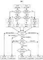
図5には、本例におけるアクセス調停装置ARBが行うアクセス調停動作を説明するフローチャートが示される。 FIG. 5 shows a flowchart for explaining the access arbitration operation performed by the access arbitration apparatus ARB in this example.
STEP1ではリード命令を含んだアクセス要求Aがアクセス調停装置ARBへ入力され、STEP7ではリード命令を含んだアクセス要求Bが入力されて動作が開始する。STEP2およびSTEP8ではリクエストバッファreq0が空いているかを確認する。リクエストバッファreq0が空いていなければSTEP4へ進み、空いていればSTEP3へ進み。STEP3ではアクセス要求Aの要求リードレイテンシRLAと転送可能リードレイテンシLaとの比較を行う。要求リードレイテンシRLAが転送可能レイテンシLaより小さい場合、つまり、要求リードレイテンシ以内にデータを転送できない場合はSTEP4へ進み、要求レイテンシRLAが転送可能レイテンシLa以上場合、つまり、要求レイテンシRLA以内にデータを転送できる場合はSTEP6に進む。 In
STEP4では、アクセス要求Aを発行したマスタへ再要求を行うことを伝える。STEP4が終了するとSTEP5へ進む。STEP5では、信号MAを0にする。 In STEP 4, the master that issued the access request A is notified that a re-request is to be made. When STEP4 ends, the process proceeds to STEP5. In STEP5, the signal MA is set to zero.
STEP6では、信号MAを1にする。 In STEP 6, the signal MA is set to 1.
STEP9ではアクセス要求Bの要求リードレイテンシRLBと転送可能リードレイテンシLaとの比較を行う。要求リードレイテンシRLBが転送可能リードレイテンシLaより小さい場合、つまり要求リードレイテンシ以内にデータを転送できない場合はSTEP10へ進み、要求リードレイテンシRLAが転送可能リードレイテンシLa以上場合、つまり、要求リードレイテンシRLB以内にデータを転送できる場合はSTEP12へ進む。STEP10では、アクセス要求Bを発行したマスタへ再要求を行うことを通知する。STEP10が終了するとSTEP11へ進む。STEP1では、信号MBを0にする。 In
STEP12では、信号MBを1にする。 In STEP 12, the signal MB is set to 1.
STEP5あるいはSTEP6、STEP11あるいはSTEP12を終了するとSTEP13へ進む。 When STEP5 or STEP6, STEP11 or STEP12 is completed, the process proceeds to STEP13.
STEP13では、信号MA及びMBの値をチェックする。信号MAが0で且つMBが0の場合、つまり、要求リードレイテンシRLA及びRLB双方とも満たせない場合、STEP16へ進む。信号MAが1で且つMBが0の場合、つまり要求リードレイテンシRLAを満たし、RLBを満たせない場合、STEP17へ進む。信号MAが1で且つMBが1の場合、つまり、要求リードレイテンシRLA及びRLB双方とも満たせる場合、STEP14へ進む。信号MAが0で且つMBが1の場合、つまり要求リードレイテンシRLAを満たせず、要求リードレイテンシRLBを満たせる場合STEP20へ進む。 In STEP 13, the values of the signals MA and MB are checked. When the signal MA is 0 and MB is 0, that is, when both of the required read latencies RLA and RLB cannot be satisfied, the process proceeds to STEP16. When the signal MA is 1 and the MB is 0, that is, when the required read latency RLA is satisfied and the RLB cannot be satisfied, the process proceeds to STEP 17. If the signal MA is 1 and the MB is 1, that is, if both the required read latencies RLA and RLB can be satisfied, the process proceeds to STEP14. If the signal MA is 0 and MB is 1, that is, if the required read latency RLA cannot be satisfied and the required read latency RLB can be satisfied, the process proceeds to STEP 20.
STE16では、アクセス調停装置ARBはメモリ制御回路へ、どちらの要求も出力しない。STEP17では、リードアクセス要求Aのみを許可し出力する。STEP20では、アクセス要求Bのみを許可し出力する。 In STE16, the access arbitrator ARB does not output either request to the memory control circuit. In STEP 17, only the read access request A is permitted and output. In STEP 20, only access request B is permitted and output.
SETP14では、アクセス要求Aの第一アクセス優先レベルPRAとアクセス要求Bの第一アクセス優先レベルPRBを比較する。アクセス要求Aの第一アクセス優先レベルPRAが、アクセス要求Bの第一アクセス優先レベルPRBより高い場合、STEP17へ進む。アクセス要求Aの第一アクセス優先レベルPRAが、アクセス要求Bの第一アクセス優先レベルPRBより低い場合、STEP20へ進む。アクセス要求Aの第一アクセス優先レベルPRAが、アクセス要求Bの第一アクセス優先レベルPRBと等しい場合、STEP15へ進む。 In SETP14, the first access priority level PRA of the access request A is compared with the first access priority level PRB of the access request B. When the first access priority level PRA of the access request A is higher than the first access priority level PRB of the access request B, the process proceeds to STEP17. When the first access priority level PRA of the access request A is lower than the first access priority level PRB of the access request B, the process proceeds to STEP20. When the first access priority level PRA of the access request A is equal to the first access priority level PRB of the access request B, the process proceeds to STEP15.
STEP15では、要求リードレイテンシRLAとRLBの値を比較する。要求リードレイテンシRLAがRLBより小さい場合はSTEP18へ進む。要求リードレイテンシRLAがRLB以上の場合はSTEP19へ進む。 In STEP 15, the values of the request read latency RLA and RLB are compared. If the requested read latency RLA is smaller than RLB, the process proceeds to STEP18. If the requested read latency RLA is equal to or greater than RLB, the process proceeds to STEP 19.
STEP18では、アクセス要求Aのみを許可し出力する。STEP19では、アクセス要求Bのみを許可し出力する。 In STEP 18, only access request A is permitted and output. In STEP 19, only access request B is permitted and output.
図6には、上記アクセス調停装置ARB内の第一アクセス優先レベル回路pri0、pri1、pri2、pri3が行う第一アクセス優先レベルの動作を説明するためのフローチャートが示される。 FIG. 6 shows a flowchart for explaining the operation of the first access priority level performed by the first access priority level circuits pri0, pri1, pri2 and pri3 in the access arbitration device ARB.
特に制限されないが、第一アクセス優先レベルは0から15段階まであり、数値が大きい方が優先レベルの上位である、初期設定が6であるとして説明する。 Although there is no particular limitation, the first access priority level is from 0 to 15 levels, and it is assumed that the larger value is the higher priority level and the initial setting is 6.
STEP1では、画像処理装置MS1からアクセス要求Bが、アクセス調停装置ARBへ入力されて動作が開始される。 In STEP1, the access request B is input from the image processing apparatus MS1 to the access arbitration apparatus ARB, and the operation is started.
STEP2では、アクセス要求Bの許可と不許可がチェックされる。アクセス要求Bが許可された場合、STEP3へ進む。不許可の場合、STEP4へ進む。STEP3では第一アクセス優先レベル回路pri1のアクセス優先レベルの値PRBを最も低い0に設定する。STEP4では、アクセス優先レベルの値PRBを1つ上げ7となる。 In STEP 2, permission / denial of access request B is checked. When the access request B is permitted, the process proceeds to STEP3. If not permitted, proceed to STEP4. In STEP 3, the access priority level value PRB of the first access priority
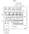
図7には、上記メモリ制御装置SL0の構成例が示される。 FIG. 7 shows a configuration example of the memory control device SL0.
上記メモリ制御装置SL0は、図7に示されるように、リクエストバッファreq0と、レスポンスバッファres0と、レジスタ回路sregと、メモリ制御回路SDCONで構成される。 As shown in FIG. 7, the memory control device SL0 includes a request buffer req0, a response buffer res0, a register circuit sreg, and a memory control circuit SDCON.
リクエストバッファreq0は、バッファrq0、rq1、rq2、rq3から構成される。レスポンスバッファres0は、バッファrs0、rs1、rs2、rs3から構成される。レジスタ回路sregはレジスタ回路regとレイテンシレジスタ回路Lregから構成される。メモリ制御回路SDCONはレイテンシ計算回路calcと、コマンド生成回路comで構成されている。 The request buffer req0 includes buffers rq0, rq1, rq2, and rq3. The response buffer res0 includes buffers rs0, rs1, rs2, and rs3. The register circuit sreg includes a register circuit reg and a latency register circuit Lreg. The memory control circuit SDCON includes a latency calculation circuit calc and a command generation circuit com.
電源投入直後、マイクロコンピュータMS0により、レジスタ回路regには、SDRAMを動作させるための命令と命令の間の最小時間(Trc,Trcd,Trp,Trwl,Tpre)と、キャスレイテンシCLと、SDRAMの入出力データバスmbusのバス幅が、例えば4Byteに設定される(図2及び図3参照)。次に、レイテンシ計算回路calcは、上記命令と命令の間の最小時間(Trc,Trcd,Trp,Trwl)と、キャスレイテンシCLを用い、読み出し時のレイテンシLacRdと、書き込み時のレイテンシLacWtと、読み出しサイクルレイテンシRcycと、書き込みサイクルレイテンシWcycとを計算し、それをレイテンシレジスタ回路Lregへ設定する。 Immediately after power-on, the microcomputer MS0 causes the register circuit reg to input the minimum time (Trc, Trcd, Trp, Trwl, Tpre) between the instructions for operating the SDRAM, the CAS latency CL, and the SDRAM input. The bus width of the output data bus mbus is set to 4 bytes, for example (see FIGS. 2 and 3). Next, the latency calculation circuit calc uses the minimum time (Trc, Trcd, Trp, Trwl) between the instructions and the instruction latency CL, the latency LacRd at the time of reading, the latency LacWt at the time of writing, and the reading The cycle latency Rcyc and the write cycle latency Wcyc are calculated and set in the latency register circuit Lreg.
読み出し時のレイテンシLacRdはTrcd+CL−1で計算され、書き込み時のレイテンシLacWtはTrcdで計算され、読み出しサイクルレイテンシRcycは読み出し時のレイテンシLacRd+Bstmax−Tpre+Trpで計算され、書き込みサイクルレイテンシWcycはTrcd−1+Bstmax+Trwl+Trpで計算される。メモリ制御回路SDCONが受け付けることのできる最大データ転送サイズが32ByteでSDRAMのデータバス幅が4Byteの場合、Bstmaxは8(=32Byte/4Byte)となる。 Latency LacRd at the time of reading is calculated by Trcd + CL-1, latency LacWt at the time of writing is calculated by Trcd, read cycle latency Rcyc is calculated by latency LacRd + Bstmax-Tpre + Trp at the time of reading, and write cycle latency Wcyc is Trcd. Calculated as -1 + Bstmax + Trwl + Trp. When the maximum data transfer size that can be accepted by the memory control circuit SDCON is 32 bytes and the data bus width of the SDRAM is 4 bytes, Bstmax is 8 (= 32 bytes / 4 bytes).
次に、メモリ制御装置SL0のリクエストバッファreq0及びレスポンスバッファres0の各バッファが全て空き状態で、アクセス要求を待っている場合の動作を説明する。 Next, the operation when the request buffer req0 and the response buffer res0 of the memory control device SL0 are all empty and waiting for an access request will be described.
メモリ制御装置SL0が要求を待っている間は、制御信号statを通じて、現時点でアクセス要求を受け付けた場合の転送可能リードレイテンシLaRNextと、転送可能ライトレイテンシLaWNextと、現在のリクエストバッファの中で、空いているリクエストバッファの数、つまり空きバッファ数を送信する。本例の場合、全てのバッファreq0からreq3の全てが、空いているリクエストバッファなので、空きバッファ数が4となる。 While the memory control device SL0 is waiting for a request, it is empty in the current request buffer through the control signal stat, the transferable read latency LaRNext when the access request is accepted at this time, the transferable write latency LaWNext, and the current request buffer. Sends the number of request buffers that are available, that is, the number of free buffers. In this example, all of the buffers req0 to req3 are free request buffers, so the number of free buffers is 4.
転送可能リードレイテンシLaRNextと、転送可能ライトレイテンシLaWNextレイテンシは計算回路calcで計算される。計算方法を以下に示す。転送可能リードレイテンシLaRNextは読み出し時のレイテンシLacRdと、読み出しサイクルレイテンシRcycと、実行待ちレイテンシpreLaとの総和となる。また、転送可能ライトレイテンシLaWNextレイテンシは、書き込み時のレイテンシLacWtと、書き込みサイクルレイテンシWcycと、実行待ちレイテンシpreLaとの総和となる。 The transferable read latency LaRNNext and the transferable write latency LaWNext latency are calculated by the calculation circuit calc. The calculation method is shown below. The transferable read latency LaRNNext is the sum of the read latency LacRd, the read cycle latency Rcyc, and the execution waiting latency preLa. Also, the transferable write latency LaWNext latency is the sum of the latency LacWt at the time of writing, the write cycle latency Wcyc, and the waiting latency latency preLa.
実行待ちレイテンシpreLaは、現アクセス要求を受け取る前に、すでに受け取ってはいるがバッファrq0からrq3に保持されて、実行待ち状態にある要求に対するレイテンシの総和である。したがって、全てのバッファrq0からrq3にアクセス要求が保持されていないので、実行待ちレイテンシpreLaは0となる。 The execution waiting latency preLa is the sum of latencies for requests that have been received but are held in the buffers rq0 to rq3 and are waiting to be executed before the current access request is received. Accordingly, since the access request is not held in all the buffers rq0 to rq3, the execution waiting latency preLa becomes 0.
次に、メモリ制御装置SL0がロード命令で16Byteのアクセス要求を受け取った場合の動作を説明する。 Next, the operation when the memory control device SL0 receives a 16-byte access request with a load command will be described.
メモリ制御回路SDCONのリクエストバッファreq0へ、リード命令、データ転送サイズ(16Byte)、転送元アドレスが保持され、アクセス要求の受け取りが完了する。受け取った直後に、レイテンシ計算回路calcは、実際にデータが要求を発行したマスタへ到達する実レイテンシLaAc及び空きリクエストバッファ数Vreqを計算する。さらに、次のアクセス要求に備えて、転送可能リードレイテンシLaRNextと、転送可能ライトレイテンシLaWNextレイテンシを計算する。その後、空きリクエストバッファ数Vreqは、1つ減り、3(=4−1)となり、信号statを通じてアクセス調停装置ARBへ転送され、実レイテンシLaAcは、信号lat4を通じてアクセス調停装置ARBへ転送され、転送可能リードレイテンシLaRNextと、転送可能ライトレイテンシLaWNextレイテンシは信号statを通じてアクセス調停装置ARBへ転送される。 The read command, the data transfer size (16 bytes), and the transfer source address are held in the request buffer req0 of the memory control circuit SDCON, and the reception of the access request is completed. Immediately after the reception, the latency calculation circuit calc calculates the actual latency LaAc and the number of free request buffers Vreq at which the data actually reaches the master that issued the request. Further, in preparation for the next access request, the transferable read latency LaRNext and the transferable write latency LaWNext latency are calculated. Thereafter, the number of free request buffers Vreq decreases by 1, becomes 3 (= 4-1), and is transferred to the access arbitration device ARB through the signal stat, and the actual latency LaAc is transferred to the access arbitration device ARB through the signal lat4 and transferred. The possible read latency LaRNNext and the transferable write latency LaWNext latency are transferred to the access arbitration device ARB through the signal stat.
次に実レイテンシLaAcの計算方法を以下に示す。 Next, the calculation method of the actual latency LaAc is shown below.
リード命令の場合、実レイテンシLaAcは、読み出し時のレイテンシLacRdと、実行待ちレイテンシpreLaの総和となり、ストア命令の場合は、書き込み時のレイテンシLacWtと、実行待ちレイテンシpreLaの総和となる。この時現アクセス要求が受け取られるまでに、バッファreq0からreq3には、実行待ちのアクセス要求が保持されていないため、実行待ちレイテンシpreLaは0である。実レイテンシLaAcを計算した後、実行待ちレイテンシpreLaを更新する。以下に新しく実行待ちレイテンシpreLaを計算し、更新する動作を示す。 In the case of a read instruction, the actual latency LaAc is the sum of the latency LacRd at the time of reading and the execution waiting latency preLa, and in the case of a store instruction, it is the sum of the latency LacWt at the time of writing and the waiting latency latency preLa. At this time, until the current access request is received, since the execution requests waiting to be executed are not held in the buffers req0 to req3, the execution waiting latency preLa is 0. After calculating the actual latency LaAc, the execution waiting latency preLa is updated. The operation of calculating and updating the new waiting latency preLa is shown below.
レイテンシ計算回路calcは、次のアクセス要求を受け取った際の実レイテンシLaAcを計算する目的と、転送可能リードレイテンシLaRNextと、転送可能ライトレイテンシLaWNextレイテンシを計算する目的で、新しく実行待ちレイテンシpreLaを計算し、更新する。新しい実行待ちレイテンシpreLaは読み出し時のレイテンシLacRdと、実サイクルレイテンシRcyAcの総和となる。 The latency calculation circuit calc calculates a new execution waiting latency preLa for the purpose of calculating the actual latency LaAc when the next access request is received, the transferable read latency LaRNNext, and the transferable write latency LaWNext latency. And update. The new execution waiting latency preLa is the sum of the latency LacRd at the time of reading and the actual cycle latency RcyAc.
次に、転送可能リードレイテンシLaRNextと、転送可能ライトレイテンシLaWNextレイテンシの計算方法を以下に示す。
転送可能リードレイテンシLaRNextは読み出し時のレイテンシLacRdと、読み出しサイクルレイテンシRcycと、更新された実行待ちレイテンシpreLaとの総和となる。Next, a method for calculating the transferable read latency LaRNNext and the transferable write latency LaWNext latency will be described below.
The transferable read latency LaRNNext is the sum of the read latency LacRd, the read cycle latency Rcyc, and the updated execution wait latency preLa.
また、転送可能ライトレイテンシLaWNextレイテンシは、書き込み時のレイテンシLacWtと、書き込みサイクルレイテンシWcycと、更新された実行待ちレイテンシpreLaとの総和となる。 The transferable write latency LaWNext latency is the sum of the latency LacWt at the time of writing, the write cycle latency Wcyc, and the updated execution wait latency preLa.
コマンド発生回路comは、リクエストバッファreq0へ入力した、リード命令、データ転送サイズ(16Byte)及びアドレスの情報に基づいて、図2に示す様に、制御信号cnt5より命令としてバンクアクテイブ命令AC、読み出し命令RD、プリチャージ命令PREを、アドレスとして、バンクアドレスBK0、ロウアドレスR0、カラムアドレスC0を出力し、メモリM0及びM1から入出力データバスmbusを通じてデータを16バイトのデータを読み出す。 Based on the read command, data transfer size (16 bytes) and address information input to the request buffer req0, the command generation circuit com, as shown in FIG. 2, receives a bank active command AC and a read command as commands from the control signal cnt5. Bank address BK0, row address R0, and column address C0 are output using RD and precharge command PRE as addresses, and 16 bytes of data are read from memories M0 and M1 through input / output data bus mbus.
読み出されたデータは、コマンド発生回路comを介し、レスポンスバッファrs0へ転送され、さらにリードデータバスtrbusを通じてアクセス調停装置ARBへ転送される。 The read data is transferred to the response buffer rs0 via the command generation circuit com, and further transferred to the access arbitration device ARB through the read data bus trbus.
以上、リード命令を受け取った場合の動作について説明したが、ライト命令を受け取った場合は、同時に、書き込みデータも受け取る。コマンド発生回路comは、図3に示されるように、制御信号cnt5より命令としてバンクアクテイブ命令AC、書き込み命令WT、プリチャージ命令PREを、アドレスとして、バンクアドレスBK0、ロウアドレスR0、カラムアドレスC0を出力し、メモリ装置M0へ入出力データバスmbusを通じて16バイトのデータを書き込む。また、レイテンシ計算回路calcは、リード命令を受け取った場合の動作と同様の動作となる。 The operation when a read command is received has been described above. When a write command is received, write data is also received at the same time. As shown in FIG. 3, the command generation circuit com receives a bank active command AC, a write command WT, and a precharge command PRE as instructions from a control signal cnt5, and a bank address BK0, a row address R0, and a column address C0 as addresses. Then, 16 bytes of data are written to the memory device M0 through the input / output data bus mbus. The latency calculation circuit calc performs the same operation as when a read command is received.
図8には、上記メモリ制御回路SDCONが計算する上述のレイテンシを、アクセス調停装置へ通達する動作説明のためのフローチャートが示される。 FIG. 8 shows a flowchart for explaining the operation for notifying the above-mentioned latency calculated by the memory control circuit SDCON to the access arbitration device.
STEP1は、メモリ制御装置SL0がアクセス要求を待っている状態である。 STEP1 is a state in which the memory control device SL0 is waiting for an access request.
STEP7では、バッファreq0からreq3に保持されているアクセス要求の実行が完了した後、バッファreq0からreq3に空き状態が新たに生じたかをチェックする。バッファreq0からreq3の空き状態が新たに生じた場合、STEP8へ進み、その空き状態が生じていない場合は、STEP9へ進む。 In STEP 7, after execution of the access request held in the buffers req0 to req3 is completed, it is checked whether a new empty state has occurred in the buffers req0 to req3. If a new empty state of the buffers req0 to req3 occurs, the process proceeds to STEP8. If the empty state does not occur, the process proceeds to STEP9.
STEP8では、実行待ちレイテンシpreLaを計算し、更新する。STEP8が終了するとSTEP9へ進む。 In
STEP9では、最新の実行待ちレイテンシpreLaを利用し、転送可能リードレイテンシLaRNext及び転送可能ライトレイテンシLaWNextを計算する。STEP9が終了するとSTEP10へ進む。 In STEP9, the latest execution waiting latency preLa is used to calculate the transferable read latency LaRNext and the transferable write latency LaWNext. When STEP9 ends, the process proceeds to STEP10.
STEP10では転送可能リードレイテンシLaRNext及び転送可能ライトレイテンシLaWNextを出力する。 In STEP 10, the transferable read latency LaRNNext and the transferable write latency LaWNext are output.
STEP2では、メモリ制御装置SL0へアクセス要求が生じた状態である。STEP3では、アクセス要求を受け取ることができるかをチェックする。要求を受け取ることができればSTEP4へ進み、受け取ることができない場合はSTEP7へ進む。STEP4では、実レイテンシLaAcを計算し、STEP5では、実行待ちレイテンシpreLaを計算し、更新する。STEP5が終了するとSTEP6へ進む。STEP6では計算した実レイテンシLaAcを出力する。 In STEP2, an access request is made to the memory control device SL0. In STEP 3, it is checked whether an access request can be received. If the request can be received, the process proceeds to STEP 4. If the request cannot be received, the process proceeds to STEP 7. In STEP 4, the actual latency LaAc is calculated, and in STEP 5, the execution waiting latency preLa is calculated and updated. When STEP5 ends, the process proceeds to STEP6. In STEP 6, the calculated actual latency LaAc is output.
図9には、上記メモリ制御装置SL0が行う空きバッファ数を通達する動作のフローチャートが示される。 FIG. 9 shows a flowchart of the operation of passing the number of empty buffers performed by the memory control device SL0.
STEP1はメモリ制御回路SDCONがアクセス要求を待っている状態である。STEP2ではメモリ制御回路SDCONへアクセス要求が生じた状態である。 STEP1 is a state in which the memory control circuit SDCON is waiting for an access request. In STEP2, an access request is made to the memory control circuit SDCON.
STEP3では、アクセス要求を受け取ることができるかをチェックする。アクセス要求を受け取ることができればSTEP4へ進み、受け取ることができない場合はSTEP6へ進む。STEP4では、空きトバッファ数を1つ減算し、STEP5では空きバッファ数を出力する。 In STEP 3, it is checked whether an access request can be received. If the access request can be received, the process proceeds to STEP4. If the access request cannot be received, the process proceeds to STEP6. In STEP 4, the number of empty buffers is decremented by 1, and in STEP 5, the number of empty buffers is output.
STEP6では、バッファrq0からrq3に保持されていたアクセス要求が実行され、完了し、バッファrq0からrq3に新たに空き状態が生じたかをチェックする。空き状態が生じていれば、STEP7へ進み、空き状態が生じていなければ、STEP5へ進む。 In STEP 6, the access request held in the buffers rq0 to rq3 is executed and completed, and it is checked whether a new empty state has occurred in the buffers rq0 to rq3. If a free state has occurred, the process proceeds to STEP 7, and if no free state has occurred, the process proceeds to STEP 5.
STEP7では、空きリクエストバッファ数Vreqを1つ加算し、STEP5では空きバッファ数を出力する。 In STEP 7, the number of empty request buffers Vreq is incremented by 1, and in STEP 5, the number of empty buffers is output.
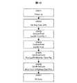
図10には、本例におけるメモリ制御回路SDCONのレジスタ回路reg及びレイテンシレジスタ回路Lregへのプログラム手順を示すフローチャートが示される。 FIG. 10 shows a flowchart showing a program procedure for the register circuit reg and the latency register circuit Lreg of the memory control circuit SDCON in this example.
STEP1は、メモリ制御回路SDCONに電源が投入された状態である。電源投入直後、STEP2へ進み、STEP2では、マイクロコンピュータMS0により、レジスタ回路regには、SDRAMを動作させるための、命令と命令の間の最小時間(Trc,Trcd,Trp,Trwl,Tpre)と、キャスレイテンシCLと、SDRAMの入出力バスmbusのバス幅が、例えば4Byteに設定される(図2及び図3参照)。次のSTEP3でレイテンシ計算回路calcは、レジスタ回路regに上記命令と命令の間の最小時間(Trc,Trcd,Trp,Trwl,Tpre)と、キャスレイテンシCLとを用い、読み出し時のレイテンシLacRdを計算する。次のSTEP4で書き込み時のレイテンシLacWtを計算する。
次のSTEP5で読み出しサイクルレイテンシRcycを計算し、次のSTEP6で書き込みサイクルレイテンシWcycを計算する。最後のSTEP7で、読み出し時のレイテンシLacRd、書き込み時のレイテンシLacWt、読み出しサイクルレイテンシRcyc、書き込みサイクルレイテンシWcycを、レイテンシレジスタ回路Lregへ設定する。 In the next STEP5, the read cycle latency Rcyc is calculated, and in the next STEP6, the write cycle latency Wcyc is calculated. In the final STEP 7, the latency LacRd at the time of reading, the latency LacWt at the time of writing, the read cycle latency Rcyc, and the write cycle latency Wcyc are set in the latency register circuit Lreg.
図11には、図8に示されるフローチャートにおけるSTEP4とSTEP5の処理の詳細が示される。 FIG. 11 shows details of the processing of STEP 4 and STEP 5 in the flowchart shown in FIG.
STEP4では、STEP41と、STEP42及びSTEP43の処理が行われる。STEP5では、STEP51と、STEP52と、STEP53と、STEP54と、STEP55と、STEP56及びSTEP57の処理が行われる。 In STEP4, STEP41 and STEP42 and STEP43 are processed. In STEP5, the processing of STEP51, STEP52, STEP53, STEP54, STEP55, STEP56 and STEP57 is performed.
STEP3では、アクセス要求を受け取ることができるかをチェックする。要求を受け取ることができればSTEP41へ進む。 In STEP 3, it is checked whether an access request can be received. If the request can be received, the process proceeds to STEP 41.
STEP41では、受け取ったアクセス要求がリード命令か、ライト命令かをチェックする。リード命令であれば、STEP42に進み、ライト命令であればSTEP43に進む。 In STEP 41, it is checked whether the received access request is a read command or a write command. If it is a read command, the process proceeds to STEP 42, and if it is a write command, the process proceeds to STEP 43.
STEP42では、読み出し時のレイテンシLacRdと実行待ちレイテンシpreLaを加算し、実レイテンシLaACを求める。その後、STEP51へ進む。STEP51では、リードサイクルレイテンシRcyACを計算する。その後、STEP52へ進む。STEP52では、リードサイクルレイテンシRcyACとサイクル時間Trcの比較を行う。リードサイクルレイテンシRcyACがサイクル時間Trc以上であればSTEP53へ進み、小さければSTEP56へ進む。 In STEP 42, the latency LacRd at the time of reading and the execution waiting latency preLa are added to obtain the actual latency LaAC. Then, it progresses to STEP51. In STEP 51, the read cycle latency RcyAC is calculated. Then, it progresses to STEP52. In STEP 52, the read cycle latency RcyAC is compared with the cycle time Trc. If the read cycle latency RcyAC is equal to or longer than the cycle time Trc, the process proceeds to STEP53, and if it is smaller, the process proceeds to STEP56.
STEP53では、リードサイクルレイテンシRcyACに、現在の実行待ちレイテンシpreLaを加算して、新たな実行待ちレイテンシpreLaを求める。STEP56では、サイクル時間Trcに、現在の実行待ちレイテンシpreLaを加算して、新たな実行待ちレイテンシpreLaを求める。 In STEP 53, the current execution wait latency preLa is added to the read cycle latency RcyAC to obtain a new execution wait latency preLa. In STEP 56, the current execution wait latency preLa is added to the cycle time Trc to obtain a new execution wait latency preLa.
STEP43では読み出し時のレイテンシLacWtと実行待ちレイテンシpreLaを加算し、実レイテンシLaACを求める。その後、STEP54へ進む。STEP54では、ライトサイクルレイテンシWcyACを計算する。その後、STEP55へ進む。STEP55では、ライトサイクルレイテンシWcyACとサイクル時間Trcの比較を行う。ライトサイクルレイテンシWcyACがサイクル時間Trc以上であればSTEP57へ進み、小さければSTEP56へ進む。 In STEP 43, the latency LacWt at the time of reading and the execution waiting latency preLa are added to obtain the actual latency LaAC. Then, it progresses to STEP54. In STEP 54, the write cycle latency WcyAC is calculated. Then, it progresses to STEP55. In STEP55, the write cycle latency WcyAC is compared with the cycle time Trc. If the write cycle latency WcyAC is equal to or longer than the cycle time Trc, the process proceeds to STEP57, and if smaller, the process proceeds to STEP56.
STEP57では、ライトサイクルレイテンシWcyACに、現在の実行待ちレイテンシpreLaを加算して、新たな実行待ちレイテンシpreLaを求める。STEP56では、サイクル時間Trcに、現在の実行待ちレイテンシpreLaを加算して、新たな実行待ちレイテンシpreLaを求める。 In STEP57, the current execution wait latency preLa is added to the write cycle latency WcyAC to obtain a new execution wait latency preLa. In STEP 56, the current execution wait latency preLa is added to the cycle time Trc to obtain a new execution wait latency preLa.
図12には、図8に示されるフローチャートのSTEP8とSTEP9との処理の詳細が示される。 FIG. 12 shows details of the processing of
STEP8では、STEP81と、STEP82と、STEP83と、STEP84と、STEP85と、STEP86と、STEP87及びSTEP88の処理を行う。STEP9では、STEP91及びSTEP92の処理を行う。 In STEP8, STEP81, STEP82, STEP83, STEP84, STEP85, STEP86, STEP87 and STEP88 are processed. In STEP9, the processing of STEP91 and STEP92 is performed.
STEP7では、バッファreq0からreq3に保持されているアクセス要求が実行され、完了し、バッファreq0からreq3に空き状態が新たに生じたかをチェックする。バッファreq0からreq3の空き状態が新たに生じた場合、STEP81へ進み、その空き状態が生じていない場合は、STEP91へ進む。 In STEP 7, the access request held in the buffers req0 to req3 is executed and completed, and it is checked whether a new empty state has occurred in the buffers req0 to req3. If a new empty state of the buffers req0 to req3 occurs, the process proceeds to STEP 81. If the empty state does not occur, the process proceeds to STEP 91.
STEP81では、受け取ったアクセス要求がリード命令かライト命令かをチェックする。リード命令であれば、STEP82へ進み、ライト命令であればSTEP86へ進む。
次のSTEP82では、リードサイクルレイテンシRcyACを計算する。次のSTEP83では、リードサイクルレイテンシRcyACとサイクル時間Trcの比較を行う。リードサイクルレイテンシRcyACがサイクル時間Trc以上であればSTEP84へ進み、小さければSTEP85へ進む。In STEP 81, it is checked whether the received access request is a read command or a write command. If it is a read command, the process proceeds to STEP 82, and if it is a write command, the process proceeds to STEP 86.
In the next STEP 82, the read cycle latency RcyAC is calculated. In the next STEP 83, the read cycle latency RcyAC is compared with the cycle time Trc. If the read cycle latency RcyAC is equal to or longer than the cycle time Trc, the process proceeds to STEP84, and if it is smaller, the process proceeds to STEP85.
STEP84では、現在の実行待ちレイテンシpreLaからリードサイクルレイテンシRcyACを減算して、新たな実行待ちレイテンシpreLaを計算する。STEP85では、現在の実行待ちレイテンシpreLaからサイクルレイテンシTrcを減算して、新たな実行待ちレイテンシpreLaを計算する。 In STEP 84, a new execution wait latency preLa is calculated by subtracting the read cycle latency RcyAC from the current execution wait latency preLa. In STEP 85, the cycle latency Trc is subtracted from the current execution waiting latency preLa to calculate a new execution waiting latency preLa.
次のSTEP86では、ライトサイクルレイテンシWcyACを計算する。次のSTEP86では、ライトサイクルレイテンシWcyACとサイクル時間Trcの比較を行う。ライトサイクルレイテンシWcyACがサイクル時間Trc以上であればSTEP88へ進み、小さければSTEP89へ進む。 In the next STEP 86, the write cycle latency WcyAC is calculated. In the next STEP 86, the write cycle latency WcyAC is compared with the cycle time Trc. If the write cycle latency WcyAC is equal to or longer than the cycle time Trc, the process proceeds to STEP 88, and if it is smaller, the process proceeds to STEP 89.
STEP88では現在の実行待ちレイテンシpreLaからライトサイクルレイテンシWcyACを減算して、新たな実行待ちレイテンシpreLaを計算する。STEP89では、現在の実行待ちレイテンシpreLaからサイクルレイテンシTrcを減算して、新たな実行待ちレイテンシpreLaを計算する。 In STEP 88, the write cycle latency WcyAC is subtracted from the current execution wait latency preLa to calculate a new execution wait latency preLa. In STEP 89, the cycle latency Trc is subtracted from the current execution waiting latency preLa to calculate a new execution waiting latency preLa.
STEP89が完了すると、次はSTEP91へ進む。STEP91では、転送可能リードレイテンシLaRNextを計算する。STEP91が完了するとSTEP92へ進む。STEP92では、転送可能ライトレイテンシLaWNextを計算する。 When STEP 89 is completed, the process proceeds to STEP 91. In STEP 91, the transferable read latency LaRNNext is calculated. When STEP 91 is completed, the process proceeds to STEP 92. In STEP 92, the transferable write latency LaWNext is calculated.
STEP92が完了するとSTEP10へ進む。STEP10では、計算した転送可能リードレイテンシLaRNextと、転送可能ライトレイテンシLaWNextを出力する。 When STEP 92 is completed, the process proceeds to STEP 10. At STEP 10, the calculated transferable read latency LaRNNext and the transferable write latency LaWNext are output.
上記実施の形態1によれば、以下の作用効果を得ることができる。 According to the first embodiment, the following operational effects can be obtained.
(1)マイクロコンピュータMS0、画像処理装置MS1、データ入力装置MS2及びデータ出力装置MS3は、常にデータの到達時間や、リクエストバッファreq0の状態を知ることができるため、データの到達時間までに、次の処理をどこまで前もって行うかを柔軟に調節することができ、マスタ内の処理を効率的に行うことができる。 (1) Since the microcomputer MS0, the image processing device MS1, the data input device MS2, and the data output device MS3 can always know the data arrival time and the state of the request buffer req0, the next time until the data arrival time is reached. It is possible to flexibly adjust how far the process is performed in advance, and the process in the master can be performed efficiently.
(2)マスタ側からの要求リードレイテンシに対して、その要求が満たされるかどうかをチェックし、さらに、要求リードレイテンシと可能リードレイテンシの差が最も小さなアクセス要求に対し、データ転送許可を与えることで、要求リードレイテンシを満たしながら、緊急度の高い要求を優先的に処理することができる。このため、必要なデータを必要な時間までに供給できシステム全体を高速にかつ円滑に動作させることが可能となる。
<実施の形態2>
図13には、上記メモリ制御装置SL0の別の構成例であるメモリ制御装置SL1が示される。尚、上記制御装置以外については上記実施の形態1と同一とされる。(2) Check whether the request is satisfied with respect to the request read latency from the master side, and further grant data transfer permission to the access request with the smallest difference between the request read latency and the possible read latency. Thus, a request with high urgency can be preferentially processed while satisfying the request read latency. Therefore, necessary data can be supplied by a necessary time, and the entire system can be operated at high speed and smoothly.
<Embodiment 2>
FIG. 13 shows a memory control device SL1 which is another configuration example of the memory control device SL0. Other than the control device is the same as that of the first embodiment.
図13に示されるメモリ制御装置SL1は、リクエストバッファreq01と、レスポンスバッファreq01と、レジスタ回路sreg1と、メモリ制御回路SDCON1で構成される。 The memory control device SL1 shown in FIG. 13 includes a request buffer req01, a response buffer req01, a register circuit sreg1, and a memory control circuit SDCON1.
リクエストバッファreq01は、バッファrq01、rq11、rq21、rq31とフラグ回路rf0,rf1,rf2,rf3から構成される。レスポンスバッファres01は、バッファrs01、rs11、rs21、rs31とフラグ回路sf0、sf1、sf2、sf3から構成される。レジスタ回路sreg1はレジスタ回路reg1とレイテンシレジスタ回路Lreg1とレジスタ回路reg2から構成される。メモリ制御回路SDCON1はレイテンシ計算回路calc1と、コマンド生成回路com1で構成されている。 The request buffer req01 includes buffers rq01, rq11, rq21, rq31, and flag circuits rf0, rf1, rf2, rf3. The response buffer res01 includes buffers rs01, rs11, rs21, rs31 and flag circuits sf0, sf1, sf2, sf3. The register circuit sreg1 includes a register circuit reg1, a latency register circuit Lreg1, and a register circuit reg2. The memory control circuit SDCON1 includes a latency calculation circuit calc1 and a command generation circuit com1.
電源投入直後、特に限定しないが、マイクロコンピュータMS0により、レジスタ回路sreg1が初期設定される。この初期設定では、先ず、信号cnt41を通じてライト命令が入力され、データバスtwbus1を通じて、バッファrq01、rq11、rq21、rq31及びバッファrs01、rs11、rs21、rs31のそれぞれが、どのマスタに利用されるかを示すバッファ利用情報が入力され、レジスタ回路reg2へ設定される。
つまり、バッファに対してバスマスタの利用権が設定され、この利用権が設定されたバッファに対しては、他のバスマスタは使用することができない。次に、レジスタ回路reg2のバッファ利用情報は、フラグ回路rf0,rf1,rf2,rf3及びフラグ回路rs0,rfs1,rfs2,rfs3へ設定される。Although there is no particular limitation immediately after the power is turned on, the register circuit sreg1 is initialized by the microcomputer MS0. In this initial setting, first, a write command is input through the signal cnt41, and to which master each of the buffers rs01, rs11, rs21, rq31 and the buffers rs01, rs11, rs21, rs31 is used via the data bus twbus1. The buffer usage information shown is input and set in the register circuit reg2.
That is, the bus master use right is set for the buffer, and other bus masters cannot use the buffer for which the use right is set. Next, the buffer usage information of the register circuit reg2 is set in the flag circuits rf0, rf1, rf2, rf3 and the flag circuits rs0, rfs1, rfs2, rfs3.
さらに、信号cnt41を通じてライト命令が入力され、データバスtwbus1を通じて、図2で示したSDRAMを動作させるための、命令と命令の間の最小時間(Trc,Trcd,Trp,Trwl)と、キャスレイテンシCLと、SDRAMの入出力バスmbus1のバス幅に関するデータが入力され、レジスタ回路reg1へ設定される。 Further, a write command is input through the signal cnt41, and the minimum time (Trc, Tcd, Trp, Trwl) between the commands and the command for operating the SDRAM shown in FIG. 2 through the data bus twbus1, and the latency CL Then, data relating to the bus width of the input / output bus mbus1 of the SDRAM is input and set in the register circuit reg1.
次に、レイテンシ計算回路calc1は、上記命令と命令の間の最小時間(Trc,Trcd,Trp,Trwl)と、キャスレイテンシCLとを用い、読み出し時のレイテンシLacRdと、書き込み時のレイテンシLacWtと、読み出しサイクルレイテンシRcycと、書き込みサイクルレイテンシWcycを計算しレイテンシレジスタ回路Lregへ設定する。 Next, the latency calculation circuit calc1 uses the minimum time (Trc, Tcd, Trp, Trwl) between the instructions and the cast latency CL, the latency LacRd at the time of reading, the latency LacWt at the time of writing, The read cycle latency Rcyc and the write cycle latency Wcyc are calculated and set in the latency register circuit Lreg.
特に制限されないが、レジスタ回路reg2のバッファ利用情報によって、フラグ回路rf0及びsf0にはデータ入力回路MS2のみが利用できるような情報が設定され、フラグ回路rf1及びsf1にはデータ出力回路MS3のみが利用できるような情報が設定され、フラグ回路rf2及びsf2には情報処理MS0のみが利用できるような情報が設定され、フラグ回路rf3及びsf3には画像処理装置MS1が利用できるような情報が設定された場合に、アクセス要求が生じた際の動作について説明する。 Although not particularly limited, information that only the data input circuit MS2 can be used is set in the flag circuits rf0 and sf0 by the buffer usage information of the register circuit reg2, and only the data output circuit MS3 is used in the flag circuits rf1 and sf1. Information that can be used is set, information that only the information processing MS0 can use is set in the flag circuits rf2 and sf2, and information that can be used by the image processing apparatus MS1 is set in the flag circuits rf3 and sf3. In this case, an operation when an access request is generated will be described.
バッファrq01はデータ入力回路MS2からのアクセス要求のみを受け付け、バッファrs01はデータ入力回路からのアクセス要求に対するレスポンスのみを処理する。バッファrq11はデータ出力回路MS3からのアクセス要求のみを受け付け、バッファrs11はデータ出力回路からのアクセス要求に対するレスポンスのみを処理する。バッファrq21はマイクロコンピュータMS0からのアクセス要求のみを受け付け、バッファrs21はマイクロコンピュータMS0及びデータからのアクセス要求に対するレスポンスのみを処理する。 The buffer rq01 accepts only an access request from the data input circuit MS2, and the buffer rs01 processes only a response to the access request from the data input circuit. The buffer rq11 accepts only an access request from the data output circuit MS3, and the buffer rs11 processes only a response to the access request from the data output circuit. Buffer rq21 accepts only access requests from microcomputer MS0, and buffer rs21 processes only responses to access requests from microcomputer MS0 and data.
rq31は画像処理装置MS1からのアクセス要求のみを受け付け、バッファrs31は画像処理装置MS1からのアクセス要求に対するレスポンスのみを処理する。 rq31 accepts only an access request from the image processing apparatus MS1, and the buffer rs31 processes only a response to the access request from the image processing apparatus MS1.
レイテンシ計算回路calc1及びコマンド生成回路com1の動作は、それぞれ実施の形態1におけるレイテンシ計算回路calc及びコマンド生成回路comと同一とされる。 The operations of the latency calculation circuit calc1 and the command generation circuit com1 are the same as those of the latency calculation circuit calc and the command generation circuit com in the first embodiment, respectively.
制御信号cnt41より、各マスタからのアクセス要求が入力される。書き込みデータはデータバスtwbus1から入力され、読み出しデータはデータバスtrbus1から出力される。制御信号stat1からは、空きバッファ数及び転送可能レイテンシ(転送可能リードレイテンシ及び転送可能ライトレイテンシ)が出力され、制御信号lat41からは、実レイテンシ(実リードレイテンシ、実ライトレイテンシ)が出力される。 An access request from each master is input from the control signal cnt41. Write data is input from the data bus twbus1, and read data is output from the data bus trbus1. From the control signal stat1, the number of empty buffers and transferable latency (transferable read latency and transferable write latency) are output, and from the control signal lat41, actual latency (actual read latency, actual write latency) is output.
制御信号cnt41よりメモリ装置MEM0を制御する命令が出力される。データバスmbus1を通じて、読み出しデータはメモリ装置MEM0からメモリ制御装置SL1へ転送され、書き込みデータは、メモリ制御装置SL1からメモリ装置MEM0へ転送される。 A command for controlling the memory device MEM0 is output from the control signal cnt41. Through the data bus mbus1, read data is transferred from the memory device MEM0 to the memory control device SL1, and write data is transferred from the memory control device SL1 to the memory device MEM0.
次に、メモリ制御装置SL1のリクエストバッファreq01内のバッファrq011とrq11、及びレスポンスバッファres01内のバッファrs01とrs11が空き状態で、アクセス要求を待っている場合の動作を説明する。 Next, an operation when the buffers rq011 and rq11 in the request buffer req01 of the memory control device SL1 and the buffers rs01 and rs11 in the response buffer res01 are empty and waiting for an access request will be described.
メモリ制御装置SL1がアクセス要求を待っている間は、状態信号stat1を通じて、現時点でアクセス要求を受け付けた場合の転送可能レイテンシと、現在のリクエストバッファの中で、空いているバッファの数、つまり空きリバッファ数をアクセス調停装置ARBへ送信する。 While the memory control device SL1 is waiting for an access request, the status signal stat1 is used to indicate the transferable latency when the access request is accepted at the present time, and the number of free buffers in the current request buffer, that is, the free space. The rebuffer number is transmitted to the access arbitrator ARB.
本例の場合、バッファreq01が空き状態であり、バッファreq01はデータ入力回路MS2のみに利用されるため、空きバッファ数が1であることを、アクセス調停装置ARBを介してデータ入力回路MS2へ伝える。 In this example, since the buffer req01 is in an empty state and the buffer req01 is used only for the data input circuit MS2, the fact that the number of empty buffers is 1 is transmitted to the data input circuit MS2 via the access arbitration device ARB. .
また、バッファreq11も空き状態であり、バッファrq1はデータ出力回路MS3のみに利用されるため、空きリクエストバッファ数が1であることを、アクセス調停装置ARBを介してデータ出力回路MS3へ伝える。 Since the buffer req11 is also in an empty state and the buffer rq1 is used only for the data output circuit MS3, the fact that the number of empty request buffers is 1 is notified to the data output circuit MS3 via the access arbitration device ARB.
バッファreq21及びreq31には要求が保持されている占有状態であり、バッファreq21とreq31は、それぞれマイクロコンピュータMS0及び画像処理装置MS1にのみ利用されるため、空きバッファ数が0であることを、アクセス調停装置ARBを介してマイクロコンピュータMS0及び画像処理装置MS1へ伝える。 Since the requests are held in the buffers req21 and req31, the buffers req21 and req31 are used only for the microcomputer MS0 and the image processing apparatus MS1, respectively. This is transmitted to the microcomputer MS0 and the image processing apparatus MS1 via the arbitration device ARB.
マイクロコンピュータMS0、画像処理装置MS1、データ入力回路MS2及びデータ出力回路MS3から、アクセス要求があった場合、アクセス調停装置はマスタが利用できるリクエストバッファに空きがあるかをチェックし、空きがあればアクセス要求をメモリ制御回路へ転送する。 When there is an access request from the microcomputer MS0, the image processing device MS1, the data input circuit MS2, and the data output circuit MS3, the access arbitration device checks whether there is an empty request buffer that can be used by the master. The access request is transferred to the memory control circuit.
マイクロコンピュータMS0及び画像処理装置MS1からのアクセス要求に対して空いているリクエストバッファが無いため、これらマスタからの要求はアクセス調停装置ARBからメモリ制御装置SL1へは転送されない。 Since there is no request buffer available for access requests from the microcomputer MS0 and the image processing device MS1, these requests from the master are not transferred from the access arbitration device ARB to the memory control device SL1.
データ入力回路MS2及び出力回路MS3からのアクセス要求に対する空いているリクエストバッファは、それぞれ一つづつ存在するので、アクセス調停装置ARBは、これらマスタからのアクセス要求をメモリ制御装置SL1へ転送する。 Since there is one free request buffer for each access request from the data input circuit MS2 and the output circuit MS3, the access arbitration device ARB transfers the access request from these masters to the memory control device SL1.
受け付けたアクセス要求はレイテンシ計算回路calc1及びメモリ制御回路ctl1によって実施の形態1と同様に処理され、実レイテンシは信号lat41から、空バッファ数及び転送可能レイテンシは状態信号stat1から出力される。 The received access request is processed in the same manner as in the first embodiment by the latency calculation circuit calc1 and the memory control circuit ctl1, and the actual latency is output from the signal lat41, and the number of empty buffers and the transferable latency are output from the status signal stat1.
以上説明した実施の形態2によれば、マスタ毎に、リクエストバッファreq01を構成するバッファrq01、rq11、rq21、rq31及び、レスポンスバッファres01を構成するバッファrs01、rs11、rs21、rs31の利用権を設定できるので、他のマスタからの要求によってリクエストバッファreq01及びレスポンスバッファres01が占有されることが無いため、アクセス競合が発生せず、必要なデータを必要な時間までに供給できシステム全体を高速にかつ円滑に動作させることが可能となる。 According to the second embodiment described above, the right to use the buffers rq01, rq11, rq21, rq31 constituting the request buffer req01 and the buffers rs01, rs11, rs21, rs31 constituting the response buffer res01 are set for each master. Since the request buffer req01 and the response buffer res01 are not occupied by a request from another master, access contention does not occur, and necessary data can be supplied by a required time, and the entire system can be performed at high speed. It is possible to operate smoothly.
さらに、メモリをアクセスするマスタは、常に、自らのアクセス要求に対するデータの転送時間を知ることができるため、次の処理を効率良く前もって実行することができ、システム全体の高速処理が可能となる。
<実施の形態3>
図14には、上記メモリ制御回路SL1の別の構成例であるメモリ制御回路SL2が示される。尚、メモリ制御回路以外については上記実施の形態1,2の場合と同一とされる。Furthermore, since the master accessing the memory can always know the data transfer time for its own access request, the next processing can be executed efficiently in advance, and high-speed processing of the entire system is possible.
<Embodiment 3>
FIG. 14 shows a memory control circuit SL2 which is another configuration example of the memory control circuit SL1. Other than the memory control circuit is the same as in the first and second embodiments.
図14に示されるメモリ制御装置SL2は、リクエストバッファreq02と、レスポンスバッファreq12と、レジスタ回路sreg2と、計算装置calc2と、メモリ制御回路SDCON2で構成される。 The memory control device SL2 shown in FIG. 14 includes a request buffer req02, a response buffer req12, a register circuit sreg2, a calculation device calc2, and a memory control circuit SDCON2.
リクエストバッファreq02は、バッファra、rq02、rq12、rq22、rq32と、フラグ回路ro0,ro1,ro2,ro3と、フラグ回路rv0,rv1,rv2,rv3を含む。レスポンスバッファres02は、バッファsa、rs02、rs12、rs22、rs32と、フラグ回路so0,so1,so2,so3と、フラグ回路sv0、sv1、sv2、sv3から構成される。 The request buffer req02 includes buffers ra, rq02, rq12, rq22, rq32, flag circuits ro0, ro1, ro2, ro3, and flag circuits rv0, rv1, rv2, rv3. The response buffer res02 includes buffers sa, rs02, rs12, rs22, rs32, flag circuits so0, so1, so2, so3, and flag circuits sv0, sv1, sv2, sv3.
フラグ回路ro0,ro1,ro2,ro3は、図13におけるフラグ回路rf0〜rf3に対応する。フラグ回路so0〜s03は図13におけるフラグ回路sf0〜sf3に対応する。レイテンシ計算回路calc2及びコマンド生成回路com2は、それぞれ実施の形態1におけるレイテンシ計算回路calc及びコマンド生成回路comと同一機能を有する。 Flag circuits ro0, ro1, ro2, and ro3 correspond to the flag circuits rf0 to rf3 in FIG. The flag circuits so0 to s03 correspond to the flag circuits sf0 to sf3 in FIG. The latency calculation circuit calc2 and the command generation circuit com2 have the same functions as the latency calculation circuit calc and the command generation circuit com in the first embodiment, respectively.
フラグ回路ro0〜ro3、及びフラグ回路so0〜so3へのフラグ設定は、電源投入直後においてマイクロコンピュータMS0が所定のブートプログラムを実行することによって可能とされる。このフラグ回路ro0〜ro3、及びフラグ回路so0〜so3においてフラグが設定されている場合には、換言すれば、バスマスタによる利用権が設定されている場合には、それに対応するバッファはバスマスタによってよって占有される。また、フラグ回路ro0〜ro3、及びフラグ回路so0〜so3においてフラグが設定されていない場合には、それに対応するバッファについて、以下の予約が可能となる。 Flags can be set in the flag circuits ro0 to ro3 and the flag circuits so0 to so3 by the microcomputer MS0 executing a predetermined boot program immediately after the power is turned on. When the flags are set in the flag circuits ro0 to ro3 and the flag circuits so0 to so3, in other words, when the right of use by the bus master is set, the corresponding buffer is occupied by the bus master. Is done. Further, when the flags are not set in the flag circuits ro0 to ro3 and the flag circuits so0 to so3, the following reservation can be made for the corresponding buffer.
バッファra及びsaは制御信号cnt42から入力されるバッファ予約命令とバッファ予約解除命令を保持する。 The buffers ra and sa hold a buffer reservation instruction and a buffer reservation release instruction input from the control signal cnt42.
フラグ回路rv0,rv1,rv2,rv3は、それぞれ、バッファrq02、rq12、rq22、rq32が、予約状態か否かを示す信号を保持している。 The flag circuits rv0, rv1, rv2, rv3 hold signals indicating whether or not the buffers rq02, rq12, rq22, rq32 are in a reserved state, respectively.
また、フラグ回路sv0,sv1,sv2,sv3は、それぞれ、バッファrs02、rs12、rs22、rs32が予約状態か否かを示す信号を保持する。 Further, the flag circuits sv0, sv1, sv2, and sv3 hold signals indicating whether or not the buffers rs02, rs12, rs22, and rs32 are in a reserved state, respectively.
レジスタ回路sreg2はレジスタ回路reg1とレイテンシレジスタ回路Lreg1 回路calc2と、コマンド生成回路ctl2で構成されている。 The register circuit sreg2 includes a register circuit reg1, a latency register circuit Lreg1, a circuit calc2, and a command generation circuit ctl2.
レジスタ回路reg1と、レイテンシレジスタ回路Lreg1と、メモリ制御回路SDCON2はレイテンシ計算回路calc2と、コマンド生成回路com2は、実施の形態1と同様の動作を行う。 The register circuit reg1, the latency register circuit Lreg1, the memory control circuit SDCON2, the latency calculation circuit calc2, and the command generation circuit com2 perform the same operations as in the first embodiment.
信号cnt52より、各マスタからのアクセス要求が入力される。書き込みデータはデータバスtwbus2から入力され、読み出しデータはデータバスtrbus2から出力される。 An access request from each master is input from the signal cnt52. Write data is input from the data bus twbus2, and read data is output from the data bus trbus2.
状態信号stat2からは、空きバッファ数及び転送可能レイテンシ(転送可能リードレイテンシ及び転送可能ライトレイテンシ)が出力され、レイテンシ信号lat42からは、実レイテンシ(実リードレイテンシ、実ライトレイテンシ)が出力される。 The number of empty buffers and transferable latency (transferable read latency and transferable write latency) are output from the status signal stat2, and the actual latency (actual read latency, actual write latency) is output from the latency signal lat42.
制御信号cnt52よりメモリ装置MEM0を制御する命令が出力される。入出力データバスmbus2を通じて、読み出しデータは、メモリ装置MEM0からメモリ制御装置SL2へ転送され、書き込みデータは、メモリ制御装置SL2からメモリ装置MEM0へ転送される。 A command for controlling the memory device MEM0 is output from the control signal cnt52. Through the input / output data bus mbus2, read data is transferred from the memory device MEM0 to the memory control device SL2, and write data is transferred from the memory control device SL2 to the memory device MEM0.
電源投入直後、マイクロコンピュータMS0がブートプログラムを実行することによって、制御信号cnt42を通じてライト命令を含んだアクセス要求が入力され、データバスtwbus2を通じて、マスタ番号mnと、マスタ番号mnに対応する最大予約バッファ数が入力されるレジスタ回路reg3へ設定される。 Immediately after the power is turned on, the microcomputer MS0 executes the boot program, whereby an access request including a write command is input through the control signal cnt42, and the master number mn and the maximum reserved buffer corresponding to the master number mn are transmitted through the data bus twbus2. The number is set in the register circuit reg3 to which the number is input.
マスタ番号及び最大予約バッファ数によって、どのマスタが、どのぐらいの数のバッファを予約可能かということがわかる。 It can be seen from the master number and the maximum number of reserved buffers which master can reserve how many buffers.
次に、信号cnt42を通じてストア命令が入力され、データバスtwbus2を通じて、図2及び図3に示されるSDRAMを動作させるための命令と命令の間の最小時間(Trc,Trcd,Trp,Trwl,Tpre)と、キャスレイテンシCLと、SDRAMの入出力バスmbus2のバス幅に関するデータが入力され、レジスタ回路reg1へ設定される。 Next, a store instruction is input through the signal cnt42, and the minimum time (Trc, Tcd, Trp, Trwl, Tpre) between the instructions for operating the SDRAM shown in FIGS. 2 and 3 through the data bus twbus2 Then, data related to the CAS latency CL and the bus width of the input / output bus mbus2 of the SDRAM is input to the register circuit reg1.
次に、レイテンシ計算回路calc2は、上記命令と命令の間の最小時間(Trc,Trcd,Trp,Trwl,CL)を用い、読み出し時のレイテンシLacRdと、書き込み時のレイテンシLacWtと、読み出しサイクルレイテンシRcycと、書き込みサイクルレイテンシWcycを計算しレイテンシレジスタ回路Lreg1へ設定する。 Next, the latency calculation circuit calc2 uses the minimum time (Trc, Tcd, Trp, Trwl, CL) between the instructions, and uses the latency LacRd at the time of reading, the latency LacWt at the time of writing, and the read cycle latency Rcyc. Then, the write cycle latency Wcyc is calculated and set in the latency register circuit Lreg1.
次に、特に制限されないがバッファrq02、rq12、rq22が、画像処理装置MS1の要求を保持しており、バッファrq32が空き状態で、バッファrs20、rs12、rs22が、画像処理装置MS1のアクセス要求に対する読み出しデータを保持しており、バッファrs32が空き状態である場合、データ出力装置MS3からアクセス要求が生じた場合の動作を説明する。 Next, although not particularly limited, the buffers rq02, rq12, and rq22 hold requests from the image processing apparatus MS1, the buffer rq32 is empty, and the buffers rs20, rs12, and rs22 respond to access requests from the image processing apparatus MS1. An operation when an access request is generated from the data output device MS3 when the read data is held and the buffer rs32 is empty will be described.
データ出力装置MS3は、制御信号cnt3よりバファ予約要求と、マスタ識別番号midの値3をアクセス調停装置ARBへ送信する。アクセス調停装置ARBは、cnt42を通じてバッファ予約要求と及びマスタ識別番号midの値3をメモリ制御装置SL2へ送信する。 The data output device MS3 transmits a buffer reservation request and the value 3 of the master identification number mid to the access arbitration device ARB from the control signal cnt3. The access arbitration device ARB transmits the buffer reservation request and the value 3 of the master identification number mid to the memory control device SL2 through the cnt42.
入力されたバッファ予約要求と及びマスタ識別番号midの値3は、バッファra及びsaへ保持される。 The input buffer reservation request and the master identification number mid value 3 are held in the buffers ra and sa.
次に、バッファraは、レジスタ回路reg3に保持されているマスタ番号mnの中に、マスタ識別番号mid値3があるかどうかチェックする。 Next, the buffer ra checks whether there is a master identification number mid value 3 among the master numbers mn held in the register circuit reg3.
識別番号mid値3と一致するマスタ番号mnが存在すれば、バッファrv0からrv3内の情報を検索し、バッファrq02からrq32の中で空いているバッファを探す。 If there is a master number mn that matches the identification number mid value 3, information in the buffers rv0 to rv3 is searched, and an empty buffer is searched in the buffers rq02 to rq32.
空き状態のバッファrq32であれば、バッファrq32に対して予約を行う。その際、バッファrv3には識別番号mid値3が保持され、バッファrq32がデータ出力装置MS3によってのみ利用可能になる。 If it is an empty buffer rq32, a reservation is made for the buffer rq32. At this time, the identification number mid value 3 is held in the buffer rv3, and the buffer rq32 can be used only by the data output device MS3.
また、バッファrq02からrq32の中で空き状態のバッファが存在しなければ、最初に空き状態となったバッファ対し予約を行う。バッファrq32が最初に空き状態となった場合、バッファrq32に対して予約を行う。その際、バッファrv3には識別番号mid値3が保持され、バッファrq32がデータ出力装置MS3によってのみ利用可能になる。 Also, if there is no empty buffer among the buffers rq02 to rq32, a reservation is made for the buffer that first becomes empty. When the buffer rq32 becomes empty first, a reservation is made for the buffer rq32. At this time, the identification number mid value 3 is held in the buffer rv3, and the buffer rq32 can be used only by the data output device MS3.
次に、バッファsaは、レジスタ回路reg3に保持されているマスタ番号mnの中に、マスタ識別番号mid値3があるかどうかチェックする。もし、識別番号mid値3と一致するマスタ番号mnが存在すれば、バッファsv0からsv3内の情報を検索し、バッファrs02からrs32の中で空いているバッファを探す。 Next, the buffer sa checks whether there is a master identification number mid value 3 among the master numbers mn held in the register circuit reg3. If there is a master number mn that matches the identification number mid value 3, information in the buffers sv0 to sv3 is searched, and an empty buffer is searched in the buffers rs02 to rs32.
空き状態のバッファrs32であれば、バッファrs32に対して予約を行う。その際、バッファsv3には識別番号mid値3が保持され、バッファrs32がデータ出力装置MS3によってのみ利用可能になる。 If the buffer rs32 is empty, a reservation is made for the buffer rs32. At this time, the identification number mid value 3 is held in the buffer sv3, and the buffer rs32 can be used only by the data output device MS3.
また、バッファrs02からrs32の中で空き状態のバッファが存在しなければ、最初に空き状態となったバッファ対し予約を行う。バッファrs32が最初に空き状態となった場合、バッファrs32に対して予約を行う。その際、バッファsv3には識別番号mid値3が保持され、バッファrs32がデータ出力装置MS3によってのみ利用可能になる。 If there is no empty buffer among the buffers rs02 to rs32, a reservation is made for the buffer that first becomes empty. When the buffer rs32 becomes empty first, a reservation is made for the buffer rs32. At this time, the identification number mid value 3 is held in the buffer sv3, and the buffer rs32 can be used only by the data output device MS3.
バッファの予約が完了すると、信号stat2より、予約が完了したこと知らせる予約完了信号及び識別番号mid値3をアクセス調停装置ARBへ送信される。その後、データ出力回路MS3から、リード命令を含んだアクセス要求が生じた場合、バッファrq32及びrs32はデータ出力回路MS3にのみ利用可能な状態となっているので、データ出力回路MS3の要求がバッファrq32へエントリーされる。その後、レイテンシ計算回路calc2及びメモリ制御回路ctl2にて処理され、メモリ装置M0よりデータが読み出されバッファrs32に転送される。次にバッファrs32はリードデータバスtrbus2からデータを、アクセス調停装置ARBへ出力する。また、識別番号mid値3は、信号stat2を通じてアクセス調停装置ARBへ送信される。 When the buffer reservation is completed, a reservation completion signal indicating that the reservation is completed and an identification number mid value 3 are transmitted to the access arbitrating device ARB from the signal stat2. Thereafter, when an access request including a read command is generated from the data output circuit MS3, the buffers rq32 and rs32 are in a state that can be used only by the data output circuit MS3. To be entered. Thereafter, the data is processed by the latency calculation circuit calc2 and the memory control circuit ctl2, and the data is read from the memory device M0 and transferred to the buffer rs32. Next, the buffer rs32 outputs the data from the read data bus trbus2 to the access arbitration device ARB. The identification number mid value 3 is transmitted to the access arbitration device ARB through the signal stat2.
アクセス調停装置ARBは、データバスrbusを通じてデータを、データ出力装置MS3へ出力する。また、信号rstatを通じて識別番号mid値3をデータ出力装置MS3へ送信する。 The access arbitration device ARB outputs data to the data output device MS3 through the data bus rbus. Further, the identification number mid value 3 is transmitted to the data output device MS3 through the signal rstat.
次に、バッファの予約解除について説明する。 Next, buffer reservation cancellation will be described.
データ出力装置MS3は、制御信号cnt3よりバッファ予約解除要求と、マスタ識別番号midの値3をアクセス調停装置ARBへ送信する。アクセス調停装置ARBは、cnt42を通じてバッファ予約解除要求と及びマスタ識別番号midの値3をメモリ制御装置SL2へ送信する。 The data output device MS3 transmits a buffer reservation cancellation request and the value 3 of the master identification number mid to the access arbitration device ARB from the control signal cnt3. The access arbitration device ARB transmits the buffer reservation cancellation request and the value 3 of the master identification number mid to the memory control device SL2 through the cnt42.
入力されたバッファ予約解除要求と及びマスタ識別番号midの値3は、バッファra及びsaへ保持される。 The input buffer reservation cancellation request and the master identification number mid value 3 are held in the buffers ra and sa.
次に、バッファraは、レジスタ回路reg3に保持されているマスタ番号mnの中に、マスタ識別番号mid値3があるかどうかチェックする。もし、識別番号mid値3と一致するマスタ番号mnが存在すれば、バッファrv0からrv3内の情報を検索し、バッファrq02からrq32の中でデータ出力装置MS3が予約しているバッファを探す。本例では、予約しているバッファrq32及びrs32に対して予約解除を行う。予約解除後は、バッファrq32及びrs32は、どのマスタにも利用可能となる。 Next, the buffer ra checks whether there is a master identification number mid value 3 among the master numbers mn held in the register circuit reg3. If there is a master number mn that matches the identification number mid value 3, information in the buffers rv0 to rv3 is searched, and a buffer reserved by the data output device MS3 is searched from the buffers rq02 to rq32. In this example, the reservation is canceled for the reserved buffers rq32 and rs32. After the reservation is released, the buffers rq32 and rs32 can be used by any master.
バッファの予約解除が完了すると、状態信号stat2より、予約解除が完了したこと知らせる予約解除完了信号及び識別番号mid値3をアクセス調停装置ARBへ送信される。さらに、アクセス調停装置ARBは信号rstatを通じて、データ出力装置MS3へ、予約解除完了信号及び識別番号mid値3を送信する。これによって、データ出力装置MS3は、予約解除が完了したことを知ることができる。また、レジスタreg3へ保持されているマスタ番号mnとマスタ識別番号mid値3とが一致するが存在しなければ、状態信号stat2を通じて、マスタ番号不一致情報と、マスタ識別番号mid値3とが、アクセス調停装置ARBへ送信される。さらに、アクセス調停装置ARBは信号rstatを通じて、データ出力装置MS3へ、マスタ番号不一致情報及び識別番号mid値3を送信する。これによって、データ出力装置MS3は、予約が不可能であることを知ることができる。 When the reservation release of the buffer is completed, a reservation release completion signal indicating that the reservation release is completed and an identification number mid value 3 are transmitted to the access arbitration device ARB from the status signal stat2. Furthermore, the access arbitration device ARB transmits a reservation cancellation completion signal and an identification number mid value 3 to the data output device MS3 through the signal rstat. As a result, the data output device MS3 can know that the reservation cancellation has been completed. If the master number mn and the master identification number mid value 3 held in the register reg3 match but do not exist, the master number mismatch information and the master identification number mid value 3 are accessed through the status signal stat2. It is transmitted to the arbitration device ARB. Further, the access arbitrating device ARB transmits the master number mismatch information and the identification number mid value 3 to the data output device MS3 through the signal rstat. Thereby, the data output device MS3 can know that the reservation is impossible.
以上説明した実施の形態によれば、マスタ毎に、リクエストバッファreq01を構成するバッファrq01、rq11、rq21、rq31及び、レスポンスバッファres01を構成するバッファrs01、rs11、rs21、rs31を必要な時間帯に必要な数を予約し、利用権を設定できるので、他のマスタからの要求によってリクエストバッファreq01及びレスポンスバッファres01が占有されることが無いため、必要な時間帯のみにアクセス競合を発生させず、必要なデータを必要な時間までに供給できシステム全体を高速にかつ円滑に動作させることが可能となる。 According to the embodiment described above, for each master, the buffers rq01, rq11, rq21, rq31 constituting the request buffer req01 and the buffers rs01, rs11, rs21, rs31 constituting the response buffer res01 are set in a necessary time zone. Since the necessary number can be reserved and the usage right can be set, the request buffer req01 and the response buffer res01 are not occupied by a request from another master, so that an access conflict does not occur only in a necessary time zone, Necessary data can be supplied by a necessary time, and the entire system can be operated at high speed and smoothly.
また、バッファra、フラグ回路rv0,rv1,rv2,rv3、バッファsa、フラグ回路sv0,sv1,sv2,sv3は、第三者によって書き換え可能とされるのに対してro0,ro1,r02,ro3、so0,so1,so2,so3はブートプログラムが実行された場合にのみ書き換え可能とされる。ブート時の書き込みは第三者にとって不可能とされるため、図14に示される構成によれば、バッファの占有状態を確実に形成することができ、しかも必要に応じて予約対応とすることができる。
<実施の形態4>
図15には、本願を適用した情報処理システムの別の構成例が示される。In addition, the buffer ra, the flag circuits rv0, rv1, rv2, rv3, the buffer sa, and the flag circuits sv0, sv1, sv2, sv3 are rewritable by a third party, whereas ro0, ro1, r02, ro3, So0, so1, so2, and so3 can be rewritten only when the boot program is executed. Since writing at the time of booting is impossible for a third party, according to the configuration shown in FIG. 14, the occupied state of the buffer can be surely formed, and reservation can be made as necessary. it can.
<Embodiment 4>
FIG. 15 shows another configuration example of the information processing system to which the present application is applied.
図15に示される情報処理システムは、中央演算回路CPUを装備するマイクロコンピュータMS0と、グラフィックス回路を装備するグラフィック処理装置MS6と、データ圧縮/伸張回路MACCを装備する画像処理装置MS1と、データ入力装置MS1と、データ出力装置MS3と、アクセス調停装置ARBと、メモリ制御装置SL2と、撮像装置CCDと、画像表示装置LCDと、メモリ装置MEM0と、内蔵メモリ装置OCRAMとを含んで構成される。そして、この情報処理装置はクロックCLKに同期して動作する。 The information processing system shown in FIG. 15 includes a microcomputer MS0 equipped with a central processing circuit CPU, a graphic processing device MS6 equipped with a graphics circuit, an image processing device MS1 equipped with a data compression / decompression circuit MACC, and data An input device MS1, a data output device MS3, an access arbitration device ARB, a memory control device SL2, an imaging device CCD, an image display device LCD, a memory device MEM0, and a built-in memory device OCRAM are configured. . The information processing apparatus operates in synchronization with the clock CLK.
特に制限されないが、マイクロコンピュータMS0、グラフィック処理装置MS6、画像処理装置MS1、データ入力装置MS2、データ出力装置MS3、アクセス調停装置ARB、メモリ制御装置SL2および内蔵メモリ装置OCRAMは同一基板CHIP4上に形成される。 Although not particularly limited, the microcomputer MS0, the graphic processing device MS6, the image processing device MS1, the data input device MS2, the data output device MS3, the access arbitration device ARB, the memory control device SL2, and the built-in memory device OCRAM are formed on the same substrate CHIP4. Is done.
特に制限されないが、メモリ装置MEM0および内蔵メモリ装置OCRAMはDRAM、SRAM及び不揮発性メモリで構成することが可能である。 Although not particularly limited, the memory device MEM0 and the built-in memory device OCRAM can be configured by DRAM, SRAM, and nonvolatile memory.
マイクロコンピュータMS0と、画像処理装置MS1と、データ入力装置MS1と、データ出力装置MS3と、アクセス調停装置ARBおよび内蔵メモリ装置OCRAMは、実施の形態1で示したそれぞれの装置と同様の動作を行う。 The microcomputer MS0, the image processing device MS1, the data input device MS1, the data output device MS3, the access arbitration device ARB, and the built-in memory device OCRAM perform the same operations as the respective devices described in the first embodiment. .
メモリ制御回路SL2には、実施の形態1,2及び3で示したメモリ制御機能を実現できるが、本例では、実施の形態3で示したメモリ制御機能を実現する。 The memory control circuit SL2 can realize the memory control function described in the first, second, and third embodiments, but in this example, the memory control function described in the third embodiment is realized.
3次元グラフィックス処理では、ジオメトリ処理を行い、その後レンダリング処理を行う。ジオメトリ処理は、特に制限されないが、マイクロコンピュータMS0が行う処理で、3次元図形を表すため、図形の座標計算を行うことである。レンダリング処理は、画像処理装置MS1が行う処理で、画像表示装置LCDへ表示するために、ジオメトリ処理後の3次元図形に、色、明るさ、奥行き、絵柄といった視覚的効果を付け足す処理である。 In the three-dimensional graphics processing, geometry processing is performed, and then rendering processing is performed. The geometry processing is not particularly limited, but is processing performed by the microcomputer MS0, and is to perform coordinate calculation of a graphic in order to represent a three-dimensional graphic. The rendering process is a process performed by the image processing apparatus MS1, and is a process for adding visual effects such as color, brightness, depth, and design to the three-dimensional figure after the geometry process for display on the image display device LCD.
3次元画像はメモリ装置MEM0へ格納されており、現在の3次元画像を読み出して、マイクロコンピュータMS0がジオメトリ処理を行い、その後、グラフィック処理装置MS6がレンダリング処理を行い、新しい3次元画像を生成し、再度メモリ装置MEM0へ格納する。最後に、生成された3次元画像は、出力装置MS3へ転送され、画像表示装置LCDへ表示される。 The three-dimensional image is stored in the memory device MEM0. The current three-dimensional image is read out, the microcomputer MS0 performs geometry processing, and then the graphic processing device MS6 performs rendering processing to generate a new three-dimensional image. Then, it is stored again in the memory device MEM0. Finally, the generated three-dimensional image is transferred to the output device MS3 and displayed on the image display device LCD.
このように、3Dグラフィックス処理において、マイクロコンピュータMS0、グラフィック処理装置MS6及び画像出力装置MS3は、メモリ装置MEM0をアクセスする。 Thus, in the 3D graphics processing, the microcomputer MS0, the graphic processing device MS6, and the image output device MS3 access the memory device MEM0.
このような3次元グラフィックス処理では、ジオメトリ処理、レンダリング処理及び表示同時に処理され、さらに1秒間に30画面分の3Dグラフィックス処理を行う必要がある。 In such 3D graphics processing, geometry processing, rendering processing, and display processing are performed simultaneously, and it is necessary to perform 3D graphics processing for 30 screens per second.
以上説明したように、グラフィックス処理を行う場合においても、本発明を適用することにより、必要なデータを必要な時間までに供給できシステム全体を高速にかつ円滑に動作させることが可能となる。 As described above, even when graphics processing is performed, by applying the present invention, necessary data can be supplied by a required time, and the entire system can be operated at high speed and smoothly.
さらに、メモリをアクセスするバスマスタは、常に、自らのアクセス要求に対するデータの転送時間を知ることができるため、次の処理を効率良く前もって実行することができ、システム全体の高速処理が可能となる。 Furthermore, since the bus master that accesses the memory can always know the data transfer time for its own access request, the next processing can be efficiently executed in advance, and high-speed processing of the entire system is possible.
動画像の録画と、3Dグラフィックス処理を同時に行う場合は、マイクロコンピュータMS0、画像処理装置MS1、グラフィック処理装置MS6、画像入力装置MS2及び画像出力装置MS3の全ての装置がバスマスタとなって、メモリ装置MEM0をアクセスする。
特に制限されないが、マイクロコンピュータMS0は、録画した動画像と3次元グラフィックス画像とが、それぞれで、書き換えられないように、メモリ装置MEM0内での格納領域を決めることができる。When recording moving images and 3D graphics processing at the same time, the microcomputer MS0, the image processing device MS1, the graphic processing device MS6, the image input device MS2, and the image output device MS3 are all bus masters, and the memory Access the device MEM0.
Although not particularly limited, the microcomputer MS0 can determine the storage area in the memory device MEM0 so that the recorded moving image and the three-dimensional graphics image are not rewritten respectively.
さらに、特に制限されないが、画像出力装置MS3は、マイクロコンピュータMS0の指示によって、表示装置LCDの画面を録画用の画面と3Dグラフィックス用の画面に分割し表示を行う。 Further, although not particularly limited, the image output device MS3 divides the screen of the display device LCD into a recording screen and a 3D graphics screen in accordance with an instruction from the microcomputer MS0.
以上説明したように、グラフィックス処理と動画像録画を同時に行う場合においても、本発明を適用することにより、必要なデータを必要な時間までに供給できシステム全体を高速にかつ円滑に動作させることが可能となる。さらに、メモリをアクセスするバスマスタは、常に、自らのアクセス要求に対するデータの転送時間を知ることができるため、次の処理を効率良く前もって実行することができ、システム全体の高速処理が可能となる。
<実施の形態5>
図16には、本願にかかる情報処理システムの別の構成例が示され。As described above, even when graphics processing and moving image recording are performed at the same time, by applying the present invention, necessary data can be supplied by a required time and the entire system can be operated at high speed and smoothly. Is possible. Furthermore, since the bus master that accesses the memory can always know the data transfer time for its own access request, the next processing can be efficiently executed in advance, and high-speed processing of the entire system is possible.
<Embodiment 5>
FIG. 16 shows another configuration example of the information processing system according to the present application.
図16に示される情報処理システムは、中央演算回路CPU0を装備するマイクロコンピュータMS0と、中央演算回路CPU1を装備する画像処理装置MS1と、データ入力装置MS2と、データ出力装置MS3と、アクセス調停装置ARBと、メモリ制御装置SL0と、撮像装置CCDと、画像表示装置LCDと、メモリ装置MEM0と、で、内蔵メモリ装置OCRAMとを含んで構成される。そして、この情報処理装置はクロックCLKに同期して動作する。 The information processing system shown in FIG. 16 includes a microcomputer MS0 equipped with a central processing circuit CPU0, an image processing device MS1 equipped with a central processing circuit CPU1, a data input device MS2, a data output device MS3, and an access arbitration device. The ARB, the memory control device SL0, the imaging device CCD, the image display device LCD, and the memory device MEM0 are configured to include a built-in memory device OCRAM. The information processing apparatus operates in synchronization with the clock CLK.
マイクロコンピュータMS0と、画像処理装置MS1と、データ入力装置MS2と、データ出力装置MS3と、アクセス調停装置ARBと、内蔵メモリ装置OCRAMは、実施の形態1で示したそれぞれの装置と同様の動作を行う。 The microcomputer MS0, the image processing device MS1, the data input device MS2, the data output device MS3, the access arbitration device ARB, and the built-in memory device OCRAM perform the same operations as the respective devices described in the first embodiment. Do.
メモリ制御装置SL0には、実施の形態1,2及び3で示したメモリ制御方法を実現できるが、本例では、実施の形態1で示したメモリ制御方法を実現する。 The memory control device SL0 can implement the memory control method described in the first, second, and third embodiments. In this example, the memory control method described in the first embodiment is realized.
特に制限されないが、マイクロコンピュータMS0、画像処理装置MS1、データ入力装置MS2、データ出力装置MS3、アクセス調停装置ARB、メモリ制御装置SL0および内蔵メモリ装置OCRAMは同一基板上に形成され、情報処理装置CHIP5を形作ることも可能である。 Although not particularly limited, the microcomputer MS0, the image processing device MS1, the data input device MS2, the data output device MS3, the access arbitration device ARB, the memory control device SL0, and the built-in memory device OCRAM are formed on the same substrate, and the information processing device CHIP5 Can also be formed.
特に制限されないが、メモリ装置MEM0および内蔵メモリ装置OCRAMはDRAM、SRAMなどの揮発性メモリ及び不揮発性メモリで構成することも可能である。 Although not particularly limited, the memory device MEM0 and the built-in memory device OCRAM can be configured by a volatile memory such as a DRAM and an SRAM and a nonvolatile memory.
マイクロコンピュータMS0は、ハードウエアで実現していたデータ圧縮/伸張処理をソフトウエアで行うことができ、画像処理装置MS1は、ハードウエアで実現していたグラフィックス処理をソフトウエアで行うことができる。 The microcomputer MS0 can perform data compression / decompression processing realized by hardware by software, and the image processing device MS1 can perform graphics processing realized by hardware by software. .
したがって、中央演算回路CPUを装備する情報処理装置を複数利用した場合においても、本発明を適用することにより、必要なデータを必要な時間までに供給できシステム全体を高速にかつ円滑に動作させることが可能となる。
さらにソフトウエアにて処理を行うことで、さまざまな圧縮/伸張の規格にすばやく対応することができる。さらに、新たな機能を容易に拡張できる。Therefore, even when a plurality of information processing devices equipped with a central processing circuit CPU are used, by applying the present invention, necessary data can be supplied by a required time, and the entire system can be operated at high speed and smoothly. Is possible.
Furthermore, by processing with software, it is possible to quickly cope with various compression / decompression standards. Furthermore, new functions can be easily expanded.
メモリをアクセスする複数のバスマスタからなる情報処理ユニットと、アクセス調停装置とメモリ制御装置とからなるメモリ制御ユニットとを別の半導体チップ上に形成してもよいが、両者を単一の半導体チップ上に形成してもよい。その場合、単一の半導体チップ上に形成された情報処理装置は、データバスrbus及びwbusを別々の半導体チップで形成するよりも幅の広いバスとすることが可能となる上に、両者の距離が短縮されるために、両者間での高速データ転送が可能となる。 An information processing unit composed of a plurality of bus masters for accessing a memory and a memory control unit composed of an access arbitration device and a memory control device may be formed on different semiconductor chips, but both are formed on a single semiconductor chip. You may form in. In this case, the information processing apparatus formed on a single semiconductor chip can make the data buses rbus and wbus wider than those formed by separate semiconductor chips, and the distance between the two. Therefore, high-speed data transfer between the two becomes possible.
更に、メモリ制御ユニットのみを他者に設計させ、或いは既に設計されている設計資産として情報処理ユニットと同一の半導体チップ上に形成してワンチップの情報処理装置とすることも可能である。 Further, only the memory control unit can be designed by others, or it can be formed on the same semiconductor chip as the information processing unit as an already designed design asset to form a one-chip information processing apparatus.
この場合、メモリ制御装置の回路等の構成を記録媒体に記録し、情報処理部の設計者或いは情報処理装置の設計者に提供することの可能である。 In this case, the configuration of the circuit of the memory control device can be recorded on a recording medium and provided to the designer of the information processing unit or the designer of the information processing device.
また、自らが半導体装置の製造を行う場合、他者が提供する情報処理ユニットに、本発明のメモリ制御ユニット或いはメモリ制御ユニットとメモリ装置とを組み合わせ、半導体装置を提供して他者に供給することも可能である。 When the semiconductor device itself is manufactured, the memory control unit of the present invention or a combination of the memory control unit and the memory device is combined with the information processing unit provided by the other person to provide the semiconductor device and supply it to the other person. It is also possible.
他方、メモリ制御ユニットをメモリ内に設けることも可能である。メモリ制御ユニットを情報処理ユニット或いはメモリモジュール内に形成することで、情報処理システムの製造者の負荷を低減することが可能となり、情報処理システムの小型化も可能となる。
また、半導体装置の製造プロセスの進歩にあわせ、メモリの一部或いは全部を情報処理装置と同一の半導体チップ上に形成することも可能である。つまりワンチップの情報処理システムの実現であり、システムの一層の小型化が可能となる。On the other hand, it is also possible to provide a memory control unit in the memory. By forming the memory control unit in the information processing unit or the memory module, it is possible to reduce the load on the manufacturer of the information processing system, and to reduce the size of the information processing system.
Further, in accordance with the progress of the manufacturing process of the semiconductor device, part or all of the memory can be formed on the same semiconductor chip as the information processing device. That is, it is a realization of a one-chip information processing system, and the system can be further downsized.
また、図17にはパッケージ例が示され、図18には、図17における線分A−A’線切断断面が示される。尚、17においては、図18におけるカバーCOVERが省略されている。図17及び図18に示されるように、単一チップにより形成された情報処理装置S−MSと、それぞれ単一チップにより形成されたメモリ装置S−ME1,S−ME2とを含むモジュールとを1つのパッケージで封止することができる。この構成は、マルチチップモジュール或いはマルチチップパッケージなどとして知られている。ここで、上記情報処理装置S−MSは、図1における情報処理装置CHIP1に対応し、メモリ装置S−ME1は、図1におけるメモリMEMOに対応する。 FIG. 17 shows a package example, and FIG. 18 shows a cross section taken along line A-A 'in FIG. In FIG. 17, the cover COVER in FIG. 18 is omitted. As shown in FIG. 17 and FIG. 18, a module including an information processing device S-MS formed of a single chip and memory devices S-
図19には、本発明にかかる情報処理装置の別の構成例が示される。図19に示されるのが、図1に示されるのと大きく相違するのは、メモリ装置MEM0とその動作を制御するメモリ制御装置SL0とが一つのメモリチップCHIP7に含まれている点である。このようにしても上記の例と同様の作用効果を奏する。 FIG. 19 shows another configuration example of the information processing apparatus according to the present invention. 19 is greatly different from that shown in FIG. 1 in that the memory device MEM0 and the memory control device SL0 for controlling the operation thereof are included in one memory chip CHIP7. Even if it does in this way, there exists an effect similar to said example.
以上、複数のバスマスタからのアクセス要求に対して、必要なデータを必要な時間までにバスマスタへ供給できる情報処理システムの実施形態を説明してきたが、本発明は上記実施形態に限定されるわけでは無く、本願発明の思想を逸脱しない範囲で、他にも様々な実施形態を採用することが可能である。 As described above, the embodiment of the information processing system that can supply necessary data to the bus master by a necessary time in response to access requests from a plurality of bus masters has been described. However, the present invention is not limited to the above embodiment. Various other embodiments can be employed without departing from the spirit of the present invention.
以上本発明者によってなされた発明を具体的に説明したが、本発明はそれに限定されるものではなく、その要旨を逸脱しない範囲で種々変更可能であることはいうまでもない。 Although the invention made by the present inventor has been specifically described above, the present invention is not limited thereto, and it goes without saying that various changes can be made without departing from the scope of the invention.
以上の説明では主として本発明者によってなされた発明をその背景となった利用分野である画像処理を可能とするシステムに適用した場合について説明したが、本発明はそれに限定されるものではなく、情報処理を可能とするシステム広く適用することができる。 In the above description, the case where the invention made mainly by the present inventor is applied to a system that enables image processing, which is the field of use behind it, has been described. However, the present invention is not limited thereto, and information The system that enables processing can be widely applied.
本発明は、複数のバスマスタを含むことを条件に適用することができる。 The present invention can be applied on condition that a plurality of bus masters are included.
MS0 マイクロコンピュータ
MS1 画像処理装置
MS2 データ入力装置
MS3 データ出力装置
CPU 中央演算回路
MACC データ圧縮/伸張回路
VIF データ入力回路
LIF データ出力回路
ARB アクセス調停装置
SL0 メモリ制御装置
SDCON メモリ制御回路
CCD 撮像装置
LCD 表示装置
MEM0 メモリ装置
OCRAM 内蔵メモリ装置
rqm0,rqm1,rqm2,rqm3,req0 リクエストバッファ
rsm0,rsm1,rsm2,rsm3,res0 レスポンスバッファ
sreg レジスタ回路
cnt0,cnt1,cnt2,cnt3,cnt4,cnt5,cnt6 制御信号
stat,rstat 状態信号
lat0,lat1,lat2,lat3,lat4,lat6 レイテンシ信号
wbus,rbus,twbus,trbus,rmrbus,rmwbus データバス
mbus 入出力データバス
CHIP1 情報処理装置
CLK クロック
Trcd,Trc,Trp,Trwl,Tpre 最小時間間隔
CL キャスレイテンシ
Bst データ転送回数
BK バンクアドレス
R0,R1 ロウアドレス
RD リード命令
C0 カラムアドレス
WT ライト命令
D0,D1,D2,D3 データ
lat0f,lat1f,lat2f,lat3f,lat4f,lat6f レイテンシ保持回路
latstat 状態信号保持回路
pri0,pri1,pri2,pri3 第一アクセス優先レベル回路
prireg 第一アクセス優先レベルレジスタ
midreg マスタ識別レジスタ
CNT1 アクセス許可回路
rq0,rq1,rq2,rq3,rs0,rs1,rs2,rs3 バッファ
reg レジスタ回路
Lreg レイテンシレジスタ回路
calc レイテンシ計算回路
com コマンド生成回路
SL1 メモリ制御装置
req01 リクエストバッファ
req11 レスポンスバッファ
sreg1 レジスタ回路
SDCON1 メモリ制御回路
rq01,rq11,rq21,rq31,rs01,rs11,rs21,rs31 バッファ
rf0,rf1,rf2,rf3,sf0,sf1,sf2 フラグ回路
sreg1 レジスタ回路
reg1,reg2 レジスタ回路
Lreg1 レイテンシレジスタ回路
SDCON1 メモリ制御回路
calc1 レイテンシ計算回路
com1 コマンド生成回路
cnt41,cnt51 制御信号
lat41 レイテンシ信号
stat1,rstat1 状態信号
twbus1,trbus1 データバス
mbus1 入出力データバス
SL2 メモリ制御装置
req02 リクエストバッファ
res02 レスポンスバッファ
sreg2 レジスタ回路
SDCON2 メモリ制御回路
rq02,rq12,rq22,rq32,rs02,rs12,rs22,rs312,ra,sa バッファ
rv0,rv1,rv2,rv3,sv0,sv1,sv2 フラグ回路
sreg2 レジスタ回路
reg1,reg3 レジスタ回路
Lreg1 レイテンシレジスタ回路
SDCON2 メモリ制御回路
Calc2 レイテンシ計算回路
com2 コマンド生成回路
cnt42,cnt52 制御信号
lat42 レイテンシ信号
stat2,rstat2 状態信号
twbus2,trbus2 データバス
mbus2 入出力データバス
MS6 情報処理装置
GRA グラフィックス回路
CPU 中央演算回路MS0 Microcomputer MS1 Image processing device MS2 Data input device MS3 Data output device CPU Central processing circuit MACC Data compression / decompression circuit VIF Data input circuit LIF Data output circuit ARB Access arbitration device SL0 Memory control device SDCON Memory control circuit CCD Imaging device LCD Display Device MEM0 Memory device OCRAM Built-in memory device rqm0, rqm1, rqm2, rqm3, req0 Request buffer rsm0, rsm1, rsm2, rsm3, res0 Response buffer sreg register circuit cnt0, cnt1, cnt2, cnt3, tnt4 rstat status signals lat0, lat1, lat2, lat3, lat4, lat6 Latency signals wbus, rbus, twbus, rbus, rmrbus, rmwbus Data bus mbus I / O data bus CHIP1 Information processing device CLK clock Trcd, Trc, Trp, Trwl, Tpre Minimum time interval CL CAS latency Bst Number of data transfers BK Bank address R0, R1 Row address RD Read instruction C0 column Address WT Write instruction D0, D1, D2, D3 Data lat0f, lat1f, lat2f, lat3f, lat4f, lat6f Latency holding circuit latstat State signal holding circuit pri0, pri1, pri2, pri3 First access priority level circuit prireg First access priority level Register midreg Master identification register CNT1 Access permission circuit rq0, rq1, rq2, rq3, rs0, rs1, rs , Rs3 buffer reg register circuit Lreg latency register circuit calc latency calculation circuit com command generation circuit SL1 memory control device req01 request buffer req11 response buffer sreg1 register circuit SDCON1 memory control circuit rq01, rq11, rq21, rs31, rs01, rs01, rs01, rs01, rs01 Buffer rf0, rf1, rf2, rf3, sf0, sf1, sf2 Flag circuit sreg1 register circuit reg1, reg2 register circuit Lreg1 latency register circuit SDCON1 memory control circuit calc1 latency calculation circuit com1 command generation circuit cnt41, cnt41 att signal rstat1 status signal twbus1, rbus1 data bus mbus1 input / output data bus SL2 memory controller req02 request buffer res02 response buffer sreg2 register circuit SDCON2 memory control circuit rq02, rq12, rq22, rq32, rs02, rs12, rs22, rs312, ra, sa buffer rv0, rv1 , rv3, sv0, sv1, sv2 flag circuit sreg2 register circuit reg1, reg3 register circuit Lreg1 latency register circuit SDCON2 memory control circuit Calc2 latency calculation circuit com2 command generation circuit cnt42, cnt52 control signal lat42 latency signal stat2 statb stat2 Data bus mbus2 Input / output data bus MS6 Information processing device GRA graphics circuit CPU Central processing circuit
Claims (5)
Translated fromJapanese上記メモリ制御装置は、複数のアクセス要求を受け付け可能なバッファを含み、
上記アクセス調停装置は、上記バスマスタからのアクセス要求を受け付けた場合に、上記メモリ制御装置における上記バッファの空きを確認して上記バスマスタからのアクセス要求を上記メモリ制御装置へ送信し、
上記メモリ制御装置は、上記アクセス調停装置から送信されたアクセス要求を受け付けた場合に、上記メモリ装置からのデータ転送又は上記メモリ装置へのデータ転送をいつまでに開始できるかという時間情報を上記アクセス調停装置に送信し、
上記アクセス調停装置は、上記メモリ制御装置から送信された上記時間情報を、上記アクセス要求にかかる上記バスマスタに送信することを特徴とする情報処理システム。A memory device, a memory control device capable of controlling the operation of the memory device, a plurality of bus masters each capable of accessing the memory device via the memory control device, andan access arbitration for performing access arbitration between the plurality of bus masters An information processing system including anapparatus ,
The memory control device includes a buffer capable of receiving a plurality of access requests,
When the access arbitration device receives an access request from the bus master, the access arbitration device confirms the availability of the buffer in the memory control device and transmits the access request from the bus master to the memory control device.
When the memory control device receives an access request transmitted from the access arbitration device, the memory control device displays time information indicating how long the data transfer from the memory device or the data transfer to the memory device can be started by the time. To the device,
The access arbitration apparatus transmits the time information transmitted from the memory control apparatus to the bus master according to the access request .
上記メモリ制御装置は、複数のアクセス要求を受け付け可能なバッファを含み、
上記アクセス調停装置は、上記バスマスタからリードにかかるアクセス要求とともに要求リードレイテンシが転送された場合、又は上記バスマスタからライトにかかるアクセス要求とともに要求ライトレイテンシが転送された場合に、上記メモリ制御装置における上記バッファの空きを確認して上記バスマスタからのアクセス要求を上記メモリ制御装置へ送信し、
上記メモリ制御装置は、上記アクセス調停装置を介して上記リードにかかるアクセス要求又は上記ライトにかかるアクセス要求を受け付けた場合に、上記リードにかかるアクセス要求毎の転送可能リードレイテンシ又は上記ライトにかかるアクセス要求毎の転送可能ライトレイテンシを計算してその計算結果を上記アクセス調停装置に転送し、
上記アクセス調停装置は、上記メモリ制御装置から転送された上記転送可能リードレイテンシ又は上記転送可能ライトレイテンシを上記バスマスタに転送し、且つ、アクセス要求毎に、上記要求リードレイテンシと上記転送可能リードレイテンシとの差、又は上記要求ライトレイテンシと上記転送可能ライトレイテンシとの差を求め、その差が小さいアクセス要求順にアクセス許可を与えることを特徴とする情報処理システム。A memory device, a memory control device capable of controlling the operation of the memorydevice , a plurality of bus masters each capable of accessing the memorydevice via the memory control device, andan access arbitration for performing access arbitration between the plurality of bus masters An information processing system including anapparatus ,
The memory control device includes a buffer capable of receiving a plurality of access requests,
When the request read latency is transferred together with the access request for reading from the bus master, or when the request write latency is transferred with the access request for writing from the bus master, the access arbitration device Sending an access request from the bus master to the memory control device after confirming buffer availability,
When the memory control device receives an access request for the read or an access request for the write via the access arbitration device, the memory control device can transfer the read latency for each access request for the read or the access for the write. The transferable write latency for each request is calculated and the calculation result is transferred to the access arbitration device.
The access arbitration device transfers the transferable read latency or the transferable write latency transferred from the memory control device to the bus master, and for each access request, the request read latency and the transferable read latency, Or a difference between the requested write latency and the transferable write latency, and granting access permission in the order of access requests with the smallest difference .
Priority Applications (4)
| Application Number | Priority Date | Filing Date | Title |
|---|---|---|---|
| JP2004352928AJP4748641B2 (en) | 2004-12-06 | 2004-12-06 | Information processing system |
| US11/292,218US7873796B2 (en) | 2004-12-06 | 2005-12-02 | Information processor system |
| US12/962,753US8429355B2 (en) | 2004-12-06 | 2010-12-08 | Information processor system |
| US13/782,158US8621158B2 (en) | 2004-12-06 | 2013-03-01 | Information processor system |
Applications Claiming Priority (1)
| Application Number | Priority Date | Filing Date | Title |
|---|---|---|---|
| JP2004352928AJP4748641B2 (en) | 2004-12-06 | 2004-12-06 | Information processing system |
Related Child Applications (1)
| Application Number | Title | Priority Date | Filing Date |
|---|---|---|---|
| JP2010249602ADivisionJP5229922B2 (en) | 2010-11-08 | 2010-11-08 | Information processing system |
Publications (2)
| Publication Number | Publication Date |
|---|---|
| JP2006163711A JP2006163711A (en) | 2006-06-22 |
| JP4748641B2true JP4748641B2 (en) | 2011-08-17 |
Family
ID=36665673
Family Applications (1)
| Application Number | Title | Priority Date | Filing Date |
|---|---|---|---|
| JP2004352928AExpired - Fee RelatedJP4748641B2 (en) | 2004-12-06 | 2004-12-06 | Information processing system |
Country Status (2)
| Country | Link |
|---|---|
| US (3) | US7873796B2 (en) |
| JP (1) | JP4748641B2 (en) |
Families Citing this family (9)
| Publication number | Priority date | Publication date | Assignee | Title |
|---|---|---|---|---|
| JP4748641B2 (en) | 2004-12-06 | 2011-08-17 | ルネサスエレクトロニクス株式会社 | Information processing system |
| EP1988463B1 (en)* | 2006-02-24 | 2012-01-04 | Fujitsu Ltd. | Memory control apparatus and memory control method |
| JP5669338B2 (en)* | 2007-04-26 | 2015-02-12 | 株式会社日立製作所 | Semiconductor device |
| WO2009047713A2 (en)* | 2007-10-11 | 2009-04-16 | Nxp B.V. | Method and system for controlling the admission of a storage means to a perpheral bus of a data reproduction system |
| US8904140B2 (en)* | 2009-05-22 | 2014-12-02 | Hitachi, Ltd. | Semiconductor device |
| US9535860B2 (en)* | 2013-01-17 | 2017-01-03 | Intel Corporation | Arbitrating memory accesses via a shared memory fabric |
| JP2014174849A (en)* | 2013-03-11 | 2014-09-22 | Toshiba Corp | Semiconductor memory device |
| JP5955936B2 (en)* | 2014-12-16 | 2016-07-20 | 株式会社日立製作所 | Semiconductor device |
| CN114490457B (en)* | 2015-10-01 | 2024-06-21 | 瑞萨电子株式会社 | Semiconductor devices |
Family Cites Families (28)
| Publication number | Priority date | Publication date | Assignee | Title |
|---|---|---|---|---|
| JPS5725054A (en)* | 1980-07-22 | 1982-02-09 | Nec Corp | Memory access control system |
| US5717440A (en)* | 1986-10-06 | 1998-02-10 | Hitachi, Ltd. | Graphic processing having apparatus for outputting FIFO vacant information |
| JPH064465A (en)* | 1992-06-24 | 1994-01-14 | Fujitsu Ltd | Common bus control method |
| JPH07210446A (en) | 1994-01-18 | 1995-08-11 | Fuji Electric Co Ltd | Priority determination device |
| JPH0863427A (en)* | 1994-08-19 | 1996-03-08 | Fuji Xerox Co Ltd | Data processor |
| JP3240863B2 (en) | 1994-12-21 | 2001-12-25 | 株式会社エフ・エフ・シー | Arbitration circuit |
| US6204864B1 (en) | 1995-06-07 | 2001-03-20 | Seiko Epson Corporation | Apparatus and method having improved memory controller request handler |
| WO1997005550A1 (en)* | 1995-07-27 | 1997-02-13 | Intel Corporation | Protocol for arbitrating access to a shared memory area using historical state information |
| US5850529A (en)* | 1995-08-11 | 1998-12-15 | Kabushiki Kaisha Toshiba | Method and apparatus for detecting a resource lock on a PCI bus |
| US5781799A (en)* | 1995-09-29 | 1998-07-14 | Cirrus Logic, Inc. | DMA controller arrangement having plurality of DMA controllers and buffer pool having plurality of buffers accessible to each of the channels of the controllers |
| US5671365A (en)* | 1995-10-20 | 1997-09-23 | Symbios Logic Inc. | I/O system for reducing main processor overhead in initiating I/O requests and servicing I/O completion events |
| US6317803B1 (en)* | 1996-03-29 | 2001-11-13 | Intel Corporation | High-throughput interconnect having pipelined and non-pipelined bus transaction modes |
| JP3151416B2 (en) | 1997-03-17 | 2001-04-03 | 株式会社日立製作所 | Data transfer control device and magnetic disk device |
| JPH10293744A (en) | 1997-04-18 | 1998-11-04 | Nec Corp | Pci bus system |
| JP3173418B2 (en)* | 1997-04-18 | 2001-06-04 | 日本電気株式会社 | Stream playback control method and machine-readable recording medium recording program |
| EP2357564A3 (en) | 1998-02-04 | 2011-11-23 | Panasonic Corporation | Memory control unit and memory control method and medium containing program for realizing the same |
| JP4234829B2 (en)* | 1998-12-03 | 2009-03-04 | パナソニック株式会社 | Memory control device |
| JP2000035778A (en) | 1998-07-17 | 2000-02-02 | Seiko Epson Corp | Memory control system, memory control method, and memory control device |
| JP2000315187A (en) | 1999-05-06 | 2000-11-14 | Matsushita Electric Ind Co Ltd | Memory control device, memory control method, and recording medium therefor |
| US6467052B1 (en)* | 1999-06-03 | 2002-10-15 | Microsoft Corporation | Method and apparatus for analyzing performance of data processing system |
| JP2001195351A (en)* | 2000-01-11 | 2001-07-19 | Nec Corp | Bus system and bus access method |
| JP2002055873A (en) | 2000-08-08 | 2002-02-20 | Sony Corp | Memory integrator |
| US6820152B2 (en)* | 2001-04-25 | 2004-11-16 | Matsushita Electric Industrial Co., Ltd. | Memory control device and LSI |
| ES2243765T3 (en)* | 2001-09-26 | 2005-12-01 | Siemens Aktiengesellschaft | PROCEDURE FOR ARBITRATION OF AN ACCESS TO A DATA BUS. |
| US7079856B2 (en)* | 2002-04-05 | 2006-07-18 | Lucent Technologies Inc. | Data flow control between a base station and a mobile station |
| JP4222251B2 (en)* | 2004-04-27 | 2009-02-12 | ソニー株式会社 | Bus arbitration apparatus and bus arbitration method |
| US7433984B2 (en)* | 2004-10-13 | 2008-10-07 | Texas Instruments Incorporated | Time-based weighted round robin arbiter |
| JP4748641B2 (en) | 2004-12-06 | 2011-08-17 | ルネサスエレクトロニクス株式会社 | Information processing system |
- 2004
- 2004-12-06JPJP2004352928Apatent/JP4748641B2/ennot_activeExpired - Fee Related
- 2005
- 2005-12-02USUS11/292,218patent/US7873796B2/ennot_activeExpired - Fee Related
- 2010
- 2010-12-08USUS12/962,753patent/US8429355B2/ennot_activeExpired - Fee Related
- 2013
- 2013-03-01USUS13/782,158patent/US8621158B2/enactiveActive
Also Published As
| Publication number | Publication date |
|---|---|
| US20110078351A1 (en) | 2011-03-31 |
| JP2006163711A (en) | 2006-06-22 |
| US7873796B2 (en) | 2011-01-18 |
| US20130179606A1 (en) | 2013-07-11 |
| US8621158B2 (en) | 2013-12-31 |
| US20060179193A1 (en) | 2006-08-10 |
| US8429355B2 (en) | 2013-04-23 |
Similar Documents
| Publication | Publication Date | Title |
|---|---|---|
| US8621158B2 (en) | Information processor system | |
| US5802576A (en) | Speculative cache snoop during DMA line update | |
| US20040107265A1 (en) | Shared memory data transfer apparatus | |
| CN102112973B (en) | Conditioning unit, coherent system, coordination approach, SIC (semiconductor integrated circuit) and image processing apparatus | |
| US20070162645A1 (en) | Communication system for data transfer between on-chip circuits | |
| KR102106541B1 (en) | Method for arbitrating shared resource access and shared resource access arbitration apparatus and shared resource apparatus access arbitration system for performing the same | |
| US8458411B2 (en) | Distributed shared memory multiprocessor and data processing method | |
| JP4198376B2 (en) | Bus system and information processing system including bus system | |
| KR20150095139A (en) | Direct Memory Access controller and system for accessing to channel buffer directly | |
| KR20030029030A (en) | Memory control method, memory control circuit using the control method, and integrated circuit device with the memory control circuit | |
| JP5229922B2 (en) | Information processing system | |
| US20080052424A1 (en) | Data access system, data access apparatus, data access integrated circuit, and data access method | |
| JP2591502B2 (en) | Information processing system and its bus arbitration system | |
| JP2001282704A (en) | Data processing apparatus, data processing method, and data processing system | |
| KR101022472B1 (en) | How to use the bus efficiently | |
| JPH0793274A (en) | Data transfer method and data transfer device | |
| US20120254552A1 (en) | Memory access remapping | |
| JP4446968B2 (en) | Data processing device | |
| US20060095637A1 (en) | Bus control device, arbitration device, integrated circuit device, bus control method, and arbitration method | |
| JP2000259494A (en) | Memory controller | |
| US8239652B2 (en) | Data processing system | |
| KR100441996B1 (en) | Direct Memory Access(DMA) Controller and control method | |
| US20080228961A1 (en) | System including virtual dma and driving method thereof | |
| JP4249741B2 (en) | Bus system and information processing system including bus system | |
| JP4409561B2 (en) | Event notification method, information processing apparatus, and processor |
Legal Events
| Date | Code | Title | Description |
|---|---|---|---|
| A621 | Written request for application examination | Free format text:JAPANESE INTERMEDIATE CODE: A621 Effective date:20070507 | |
| A711 | Notification of change in applicant | Free format text:JAPANESE INTERMEDIATE CODE: A712 Effective date:20100507 | |
| A131 | Notification of reasons for refusal | Free format text:JAPANESE INTERMEDIATE CODE: A131 Effective date:20100907 | |
| A521 | Request for written amendment filed | Free format text:JAPANESE INTERMEDIATE CODE: A523 Effective date:20101108 | |
| TRDD | Decision of grant or rejection written | ||
| A01 | Written decision to grant a patent or to grant a registration (utility model) | Free format text:JAPANESE INTERMEDIATE CODE: A01 Effective date:20110512 | |
| A01 | Written decision to grant a patent or to grant a registration (utility model) | Free format text:JAPANESE INTERMEDIATE CODE: A01 | |
| A61 | First payment of annual fees (during grant procedure) | Free format text:JAPANESE INTERMEDIATE CODE: A61 Effective date:20110512 | |
| R150 | Certificate of patent or registration of utility model | Ref document number:4748641 Country of ref document:JP Free format text:JAPANESE INTERMEDIATE CODE: R150 Free format text:JAPANESE INTERMEDIATE CODE: R150 | |
| FPAY | Renewal fee payment (event date is renewal date of database) | Free format text:PAYMENT UNTIL: 20140527 Year of fee payment:3 | |
| S531 | Written request for registration of change of domicile | Free format text:JAPANESE INTERMEDIATE CODE: R313531 | |
| R350 | Written notification of registration of transfer | Free format text:JAPANESE INTERMEDIATE CODE: R350 | |
| LAPS | Cancellation because of no payment of annual fees |