JP4745356B2 - Memory system - Google Patents
Memory systemDownload PDFInfo
- Publication number
- JP4745356B2 JP4745356B2JP2008051477AJP2008051477AJP4745356B2JP 4745356 B2JP4745356 B2JP 4745356B2JP 2008051477 AJP2008051477 AJP 2008051477AJP 2008051477 AJP2008051477 AJP 2008051477AJP 4745356 B2JP4745356 B2JP 4745356B2
- Authority
- JP
- Japan
- Prior art keywords
- storage area
- data
- logical
- logical block
- track
- Prior art date
- Legal status (The legal status is an assumption and is not a legal conclusion. Google has not performed a legal analysis and makes no representation as to the accuracy of the status listed.)
- Expired - Fee Related
Links
Images


Classifications
- G—PHYSICS
- G06—COMPUTING OR CALCULATING; COUNTING
- G06F—ELECTRIC DIGITAL DATA PROCESSING
- G06F12/00—Accessing, addressing or allocating within memory systems or architectures
- G06F12/02—Addressing or allocation; Relocation
- G06F12/0223—User address space allocation, e.g. contiguous or non contiguous base addressing
- G06F12/023—Free address space management
- G06F12/0238—Memory management in non-volatile memory, e.g. resistive RAM or ferroelectric memory
- G06F12/0246—Memory management in non-volatile memory, e.g. resistive RAM or ferroelectric memory in block erasable memory, e.g. flash memory
- G—PHYSICS
- G06—COMPUTING OR CALCULATING; COUNTING
- G06F—ELECTRIC DIGITAL DATA PROCESSING
- G06F12/00—Accessing, addressing or allocating within memory systems or architectures
- G06F12/02—Addressing or allocation; Relocation
- G—PHYSICS
- G06—COMPUTING OR CALCULATING; COUNTING
- G06F—ELECTRIC DIGITAL DATA PROCESSING
- G06F12/00—Accessing, addressing or allocating within memory systems or architectures
- G06F12/02—Addressing or allocation; Relocation
- G06F12/06—Addressing a physical block of locations, e.g. base addressing, module addressing, memory dedication
- G—PHYSICS
- G06—COMPUTING OR CALCULATING; COUNTING
- G06F—ELECTRIC DIGITAL DATA PROCESSING
- G06F12/00—Accessing, addressing or allocating within memory systems or architectures
- G06F12/02—Addressing or allocation; Relocation
- G06F12/08—Addressing or allocation; Relocation in hierarchically structured memory systems, e.g. virtual memory systems
- G06F12/0802—Addressing of a memory level in which the access to the desired data or data block requires associative addressing means, e.g. caches
- G06F12/0804—Addressing of a memory level in which the access to the desired data or data block requires associative addressing means, e.g. caches with main memory updating
- G—PHYSICS
- G06—COMPUTING OR CALCULATING; COUNTING
- G06F—ELECTRIC DIGITAL DATA PROCESSING
- G06F12/00—Accessing, addressing or allocating within memory systems or architectures
- G06F12/02—Addressing or allocation; Relocation
- G06F12/08—Addressing or allocation; Relocation in hierarchically structured memory systems, e.g. virtual memory systems
- G06F12/0802—Addressing of a memory level in which the access to the desired data or data block requires associative addressing means, e.g. caches
- G06F12/0893—Caches characterised by their organisation or structure
- G06F12/0897—Caches characterised by their organisation or structure with two or more cache hierarchy levels
- G—PHYSICS
- G06—COMPUTING OR CALCULATING; COUNTING
- G06F—ELECTRIC DIGITAL DATA PROCESSING
- G06F13/00—Interconnection of, or transfer of information or other signals between, memories, input/output devices or central processing units
- G06F13/14—Handling requests for interconnection or transfer
- G06F13/16—Handling requests for interconnection or transfer for access to memory bus
- G—PHYSICS
- G06—COMPUTING OR CALCULATING; COUNTING
- G06F—ELECTRIC DIGITAL DATA PROCESSING
- G06F12/00—Accessing, addressing or allocating within memory systems or architectures
- G06F12/02—Addressing or allocation; Relocation
- G06F12/08—Addressing or allocation; Relocation in hierarchically structured memory systems, e.g. virtual memory systems
- G06F12/0802—Addressing of a memory level in which the access to the desired data or data block requires associative addressing means, e.g. caches
- G06F12/0866—Addressing of a memory level in which the access to the desired data or data block requires associative addressing means, e.g. caches for peripheral storage systems, e.g. disk cache
- G—PHYSICS
- G06—COMPUTING OR CALCULATING; COUNTING
- G06F—ELECTRIC DIGITAL DATA PROCESSING
- G06F2212/00—Indexing scheme relating to accessing, addressing or allocation within memory systems or architectures
- G06F2212/10—Providing a specific technical effect
- G06F2212/1016—Performance improvement
- G—PHYSICS
- G06—COMPUTING OR CALCULATING; COUNTING
- G06F—ELECTRIC DIGITAL DATA PROCESSING
- G06F2212/00—Indexing scheme relating to accessing, addressing or allocation within memory systems or architectures
- G06F2212/72—Details relating to flash memory management
- G06F2212/7203—Temporary buffering, e.g. using volatile buffer or dedicated buffer blocks
Landscapes
- Engineering & Computer Science (AREA)
- Theoretical Computer Science (AREA)
- Physics & Mathematics (AREA)
- General Engineering & Computer Science (AREA)
- General Physics & Mathematics (AREA)
- Read Only Memory (AREA)
- Techniques For Improving Reliability Of Storages (AREA)
- Memory System Of A Hierarchy Structure (AREA)
- Memory System (AREA)
Description
Translated fromJapanese本発明は、不揮発性半導体メモリを用いて構成されるメモリシステムに関する。 The present invention relates to a memory system configured using a nonvolatile semiconductor memory.
コンピュータシステムに用いられる外部記憶装置として、NAND型フラッシュメモリなどの不揮発性半導体メモリを搭載したSSD(Solid State Drive)が注目されている。NAND型フラッシュメモリは、磁気ディスク装置に比べ、高速、軽量などの利点を有している。 As an external storage device used in a computer system, an SSD (Solid State Drive) equipped with a nonvolatile semiconductor memory such as a NAND flash memory has attracted attention. NAND flash memory has advantages such as high speed and light weight compared with a magnetic disk device.
SSD内には、複数のフラッシュメモリチップ、ホスト装置からの要求に応じて各フラッシュメモリチップのリード/ライト制御を行うコントローラ、各フラッシュメモリチップとホスト装置との間でデータ転送を行うためのバッファメモリ、電源回路、ホスト装置に対する接続インタフェースなどを備えている(例えば、特許文献1参照。)。 In the SSD, there are a plurality of flash memory chips, a controller that performs read / write control of each flash memory chip in response to a request from the host device, and a buffer for performing data transfer between each flash memory chip and the host device A memory, a power supply circuit, a connection interface for a host device, and the like are provided (for example, see Patent Document 1).
不揮発性半導体メモリには、NAND型フラッシュメモリのように、データを記憶させる場合にブロック単位で一度データを消去してからその後に書き込みを行うもの、ページ単位で書き込み/読み出しを行うものなど、消去/書き込み/読み出しの単位が固定されているものがある。 Non-volatile semiconductor memory, such as NAND flash memory, erases data that is erased once in blocks and then written, or that performs writing / reading in pages. Some units have fixed / write / read units.
一方、パーソナルコンピュータなどのホスト装置がハードディスクをはじめとする2次記憶装置に対してデータの書き込み/読み出しを行う単位は、セクタと呼ばれる。セクタは、半導体記憶装置の消去/書き込み/読み出しの単位とは独立に定められる。 On the other hand, a unit in which a host device such as a personal computer writes / reads data to / from a secondary storage device such as a hard disk is called a sector. The sector is determined independently of the unit of erasing / writing / reading of the semiconductor memory device.
例えば、不揮発性半導体メモリのブロックの大きさ(ブロックサイズ)は、512kB、ページの大きさ(ページサイズ)は、4kBであるのに対して、ホスト装置のセクタの大きさ(セクタサイズ)は、512Bのように定められている。 For example, the block size (block size) of the nonvolatile semiconductor memory is 512 kB and the page size (page size) is 4 kB, whereas the sector size (sector size) of the host device is It is determined as 512B.
このように、不揮発性半導体メモリの消去/書き込み/読み出しの単位は、ホスト装置の書き込み/読み出しの単位よりも大きい場合がある。 As described above, the erase / write / read unit of the nonvolatile semiconductor memory may be larger than the write / read unit of the host device.
そこで、不揮発性半導体メモリを用いてハードディスクのようなパーソナルコンピュータの2次記憶装置を構成する場合、ホスト装置としてのパーソナルコンピュータからの小さなサイズのデータは、不揮発性半導体メモリのブロックサイズ、ページサイズに適合させて書き込みを行う必要がある。 Therefore, when a non-volatile semiconductor memory is used to constitute a secondary storage device of a personal computer such as a hard disk, small-size data from the personal computer as a host device is stored in the block size and page size of the non-volatile semiconductor memory. It is necessary to write in conformity.
また、パーソナルコンピュータなどのホスト装置が記録するデータは、時間的局所性、および領域的局所性を兼ね備えている(例えば、非特許文献1参照。)。そのため、データを記録する際に外部から指定されたアドレスにそのまま記録していくと、特定の領域に短時間に書き換え、すなわち消去処理が集中し、消去回数の偏りが大きくなる。そのため、NAND型フラッシュメモリでは、データ更新箇所を均等に分散させるウェアレベリングと呼ばれる処理が行われる。 Data recorded by a host device such as a personal computer has both temporal locality and regional locality (see, for example, Non-Patent Document 1). For this reason, if data is recorded as it is at an address designated from the outside as it is, rewriting, that is, erasing processing concentrates in a specific area in a short time, and the number of times of erasure becomes large. For this reason, in the NAND flash memory, a process called wear leveling is performed in which data update locations are evenly distributed.
ウェアレベリング処理では、例えば、ホスト装置から指定される論理アドレスを、データ更新箇所が均等に分散された不揮発性半導体メモリの物理アドレスにアドレス変換している。 In the wear leveling process, for example, a logical address designated by the host device is converted into a physical address of a nonvolatile semiconductor memory in which data update locations are evenly distributed.
また、フラッシュメモリとホスト装置との間に、キャッシュメモリを介在させて、フラッシュメモリでの書き込み回数(消去回数)を減らすように構成されたSSDが開示されている(特許文献2参照。)。このようなキャッシュメモリを有する構成の場合、ホスト装置からの書き込み要求が発生し、且つ、キャッシュメモリが満杯のときには、キャッシュメモリのデータをフラッシュメモリに追い出す処理が行われる。 In addition, an SSD is disclosed in which a cache memory is interposed between the flash memory and the host device to reduce the number of times of writing (erasing number) in the flash memory (see Patent Document 2). In the case of such a configuration having a cache memory, when a write request from the host device is generated and the cache memory is full, a process of expelling the data in the cache memory to the flash memory is performed.
本発明は、ホスト装置に対するコマンド処理応答を規定時間内に収めることが可能なメモリシステムを提供する。 The present invention provides a memory system capable of keeping a command processing response to a host device within a specified time.
本願発明の一態様によれば、ホスト装置に対し第1の単位で読み出し/書き込みが行われる揮発性の半導体記憶素子から構成される書き込み用のキャッシュメモリとしての第1の記憶部と、第2の単位で読み出し/書き込みが行われ、前記第2の単位の2以上の自然数倍である第3の単位で消去が行われる不揮発性の半導体記憶素子から構成される第2の記憶部と、前記第3の単位の2以上の自然数分の1である第4の単位で読み出し/書き込みが行われ、前記第3の単位で消去が行われる不揮発性の半導体記憶素子から構成される第3の記憶部と、前記第2の単位で読み出し/書き込みが行われ、前記第3の単位で消去が行われる不揮発性の半導体記憶素子から構成され、前記第2の記憶部の入力バッファとして機能する第1の入力バッファと、前記第4の単位で読み出し/書き込みが行われ、前記第3の単位で消去が行われる不揮発性の半導体記憶素子から構成され、前記第3の記憶部の入力バッファとして機能する第2の入力バッファと、ホスト装置からの前記第1の単位からなる複数のデータを前記第1の記憶部に書き込む第1の処理と、前記第1の記憶部に書き込まれた複数のデータを前記第1、第2の入力バッファに追い出す第2の処理と、前記第1、第2の入力バッファに書き込まれた複数のデータを、前記第2、第3の記憶部にそれぞれ追い出し、前記第2の記憶部に書き込まれた複数のデータを第2の入力バッファに追い出す第3の処理と、を実行するコントローラと、を備えるメモリシステムであって、前記第1の入力バッファには、前記第1の記憶部以上の記憶容量を有し、前記第1の記憶部に書込まれたデータを格納する退避バッファが設けられていることを特徴とする。 According to one aspect of the present invention, a first storage unit as a cache memory for writing composed of a volatile semiconductor memory element that is read / written to / from a host device in a first unit; A second storage unit including a non-volatile semiconductor storage element that is read / written in units of and is erased in a third unit that is a natural number multiple of 2 or more of the second unit; A third semiconductor memory element is formed of a nonvolatile semiconductor memory element in which reading / writing is performed in a fourth unit that is a natural fraction of two or more of the third unit, and erasing is performed in the third unit. A memory unit and a non-volatile semiconductor memory element that is read / written in the second unit and erased in the third unit, and functions as an input buffer of the
また、本願発明の一態様によれば、ホスト装置に対し第1の単位で読み出し/書き込みが行われる揮発性の半導体記憶素子から構成される書き込み用のキャッシュメモリとしての第1の記憶部と、第2の単位で読み出し/書き込みが行われ、前記第2の単位の2以上の自然数倍である第3の単位で消去が行われる不揮発性の半導体記憶素子から構成される第2の記憶部と、前記第3の単位の2以上の自然数分の1である第4の単位で読み出し/書き込みが行われ、前記第3の単位で消去が行われる不揮発性の半導体記憶素子から構成される第3の記憶部と、前記第第2の単位で読み出し/書き込みが行われ、前記第3の単位で消去が行われる不揮発性の半導体記憶素子から構成される第4の記憶部と、前記第2の単位で読み出し/書き込みが行われ、前記第3の単位で消去が行われる不揮発性の半導体記憶素子から構成され、前記第2の記憶部の入力バッファとして機能する第1の入力バッファと、前記第4の単位で読み出し/書き込みが行われ、前記第3の単位で消去が行われる不揮発性の半導体記憶素子から構成され、前記第3の記憶部の入力バッファとして機能する第2の入力バッファと、前記第2の単位で読み出し/書き込みが行われ、前記第3の単位で消去が行われる不揮発性の半導体記憶素子から構成され、前記第4の記憶部の入力バッファとして機能する第3の入力バッファと、ホスト装置からの前記第1の単位からなる複数のデータを前記第1の記憶部に書き込む第1の処理と、前記第1の記憶部に書き込まれた複数のデータを前記第1、第2の入力バッファに追い出す第2の処理と、前記第1、第2の入力バッファに書き込まれた複数のデータを、前記第2、第3の記憶部にそれぞれ追い出し、前記第2の記憶部に書き込まれた複数のデータを第2の入力バッファに追い出す第3の処理と、前記第2の記憶部に書き込まれた複数のデータを第3の単位で第4の記憶部に追い出し、前記第4の記憶部に書き込まれた複数のデータを第3の単位で第3の入力バッファに追い出す第4の処理と、を実行するコントローラと、を備えるメモリシステムであって、前記第1の入力バッファには、前記第1の記憶部以上の記憶容量を有し、前記第1の記憶部に書込まれたデータを格納する退避バッファが設けられていることを特徴とする。 In addition, according to one aspect of the present invention, a first storage unit as a write cache memory composed of a volatile semiconductor storage element that is read / written to / from the host device in a first unit; A second storage unit configured by a nonvolatile semiconductor storage element that is read / written in the second unit and erased in a third unit that is a natural number multiple of 2 or more of the second unit. Read / write is performed in a fourth unit which is a natural fraction of two or more of the third unit, and erase is performed in the third unit. 3 storage units, a fourth storage unit composed of a nonvolatile semiconductor memory element that is read / written in the second unit and erased in the third unit, and the second unit Read / write in units of A first input buffer configured as a non-volatile semiconductor memory element that is erased in the third unit and functioning as an input buffer of the second memory unit; and reading / writing in the fourth unit And a second input buffer functioning as an input buffer of the third storage unit, and reading in the second unit A third input buffer that is configured by a nonvolatile semiconductor memory element that is written and erased in the third unit and functions as an input buffer of the fourth memory unit; A first process for writing a plurality of data composed of a first unit to the first storage unit, and a plurality of data written to the first storage unit to the first and second input buffers. A second process to be output, and a plurality of data written in the first and second input buffers are respectively driven out to the second and third storage units, and a plurality of data written in the second storage unit A third process for expelling data to the second input buffer and a plurality of data written in the second storage unit are expelled to the fourth storage unit in a third unit and written to the fourth storage unit And a controller that executes a fourth process for expelling the plurality of pieces of data to a third input buffer in a third unit, wherein the first input buffer includes the first process And a storage buffer for storing data written in the first storage unit.
本発明によれば、ホスト装置に対するコマンド処理応答を規定時間内に収めることができるという効果を奏する。 According to the present invention, there is an effect that a command processing response to the host device can be kept within a specified time.
以下、本発明の実施の形態について図面を参照して説明する。なお、以下の説明において、同一の機能および構成を有する要素については、同一符号を付し、重複説明は必要な場合にのみ行う。 Hereinafter, embodiments of the present invention will be described with reference to the drawings. In the following description, elements having the same function and configuration are denoted by the same reference numerals, and redundant description will be given only when necessary.
先ず、本明細書で用いる用語について定義しておく。
・物理ページ:NANDメモリチップ内部において一括して書き込み/読み出しが可能な単位のこと。物理ページサイズは、例えば4kB。ただし、主データ(ユーザデータなど)に対してSSD内で付加される誤り訂正符号などの冗長ビットは含まないものとする。通常、4kB+冗長ビット(例えば、数10B)が同時にメモリセルに書き込まれる単位となるが、説明の便宜上、上記のように定義する。
・論理ページ:SSD内で設定される書き込み/読み出し単位であり、1以上の物理ページに対応付けられている。論理ページサイズは、例えば8ビットノーマルモードでは、4kB、32ビット倍速モードでは、32kB。ただし、冗長ビットは含まないものとする。
・物理ブロック:NANDメモリチップ内部において独立して消去可能な最小単位のことであり、複数の物理ページから構成される。物理ブロックサイズは、例えば512kB。ただし、主データに対してSSD内で付加される誤り訂正符号などの冗長ビットは含まないものとする。通常、512kB+冗長ビット(例えば、数10kB)が同時に消去される単位となるが、説明の便宜上、上記のように定義する。
・論理ブロック:SSD内で設定される消去単位であり、1以上の物理ブロックに対応付けられている。論理ブロックサイズは、例えば8ビットノーマルモードでは、512kB、32ビット倍速モードでは、4MB。ただし、冗長ビットは含まないものとする。
・セクタ:ホストからの最小アクセス単位のこと。セクタサイズは、例えば512B。
・クラスタ:SSD内で「小さなデータ」を管理する管理単位。クラスタサイズはセクタサイズ以上であり、クラスタサイズの2以上の自然数倍が論理ページサイズとなるように定められる。
・トラック:SSD内で「大きなデータ」を管理する管理単位。クラスタサイズの2以上の自然数倍がトラックサイズに、かつ、トラックサイズの2以上の自然数倍が論理ブロックサイズとなるように定められる。
・フリーブロック(FB):用途未割り当てのNAND型フラッシュメモリ上の論理ブロックのこと。用途を割り当てる際に消去してから使用する。
・バッドブロック(BB):NAND型フラッシュメモリ上の、誤りが多いなど記憶領域として使用できない物理ブロックのこと。例えば、消去動作が正常に終了しなかった物理ブロックがバッドブロックBBとして登録される。
・書き込み効率:所定期間内における、ホストから書き込んだデータ量に対する、論理ブロックの消去量の統計値のこと。小さいほどNAND型フラッシュメモリの消耗度が小さい。
・有効クラスタ:最新のデータを保持しているクラスタ。
・無効クラスタ:最新ではないデータを保持しているクラスタ。
・有効トラック:最新のデータを保持しているトラック。
・無効トラック:最新ではないデータを保持しているトラック。
・コンパクション:管理対象内の論理ブロックから、有効クラスタや有効トラックのみを取り出して、新しい論理ブロックに書き直すこと。First, terms used in this specification are defined.
Physical page: A unit that can be written / read collectively in the NAND memory chip. The physical page size is 4 kB, for example. However, redundant bits such as error correction codes added in the SSD to main data (user data, etc.) are not included. Normally, 4 kB + redundant bit (for example, several tens of bytes) is a unit to be simultaneously written in the memory cell, but for convenience of explanation, it is defined as described above.
Logical page: A write / read unit set in the SSD, and is associated with one or more physical pages. The logical page size is, for example, 4 kB in the 8-bit normal mode and 32 kB in the 32-bit double speed mode. However, redundant bits are not included.
Physical block: the smallest unit that can be independently erased inside the NAND memory chip, and is composed of a plurality of physical pages. The physical block size is, for example, 512 kB. However, redundant bits such as an error correction code added to the main data in the SSD are not included. Normally, 512 kB + redundant bit (for example, several tens of kB) is a unit to be erased at the same time, but for convenience of explanation, it is defined as described above.
Logical block: An erasing unit set in the SSD, and is associated with one or more physical blocks. The logical block size is, for example, 512 kB in the 8-bit normal mode and 4 MB in the 32-bit double speed mode. However, redundant bits are not included.
Sector: The minimum access unit from the host. The sector size is, for example, 512B.
Cluster: A management unit that manages “small data” in the SSD. The cluster size is equal to or larger than the sector size, and is determined so that a natural number multiple of 2 or more of the cluster size becomes the logical page size.
Track: A management unit that manages “big data” in the SSD. It is determined that a natural number multiple of 2 or more of the cluster size is a track size, and a natural number multiple of 2 or more of the track size is a logical block size.
Free block (FB): A logical block on a NAND flash memory to which no use is assigned. Use it after erasing it when assigning usages.
Bad block (BB): A physical block on a NAND flash memory that cannot be used as a storage area due to many errors. For example, a physical block for which the erase operation has not ended normally is registered as a bad block BB.
Write efficiency: A statistical value of the erase amount of a logical block with respect to the amount of data written from a host within a predetermined period. The smaller the size, the smaller the consumption of the NAND flash memory.
Valid cluster: A cluster that holds the latest data.
Invalid cluster: A cluster that holds data that is not up-to-date.
Valid track: A track that holds the latest data.
Invalid track: A track that holds data that is not up-to-date.
Compaction: Extracting only valid clusters and valid tracks from the logical block within the management target and rewriting them into a new logical block.
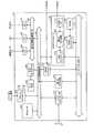
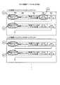
図1は、SSD(Solid State Drive)100の構成例を示すブロック図である。SSD100は、ATAインタフェース(ATA I/F)2などのメモリ接続インタフェースを介してパーソナルコンピュータあるいはCPUコアなどのホスト装置1と接続され、ホスト装置1の外部メモリとして機能する。また、SSD100は、RS232Cインタフェース(RS232C I/F)などの通信インタフェース3を介して、デバッグ用/製造検査用機器200との間でデータを送受信することができる。SSD100は、不揮発性半導体メモリとしてのNAND型フラッシュメモリ(以下、NANDメモリと略す)10と、コントローラとしてのドライブ制御回路4と、揮発性半導体メモリとしてのDRAM20と、電源回路5と、状態表示用のLED6と、ドライブ内部の温度を検出する温度センサ7と、フューズ8とを備えている。 FIG. 1 is a block diagram illustrating a configuration example of an SSD (Solid State Drive) 100. The SSD 100 is connected to a
電源回路5は、ホスト装置1側の電源回路から供給される外部直流電源から複数の異なる内部直流電源電圧を生成し、これら内部直流電源電圧をSSD100内の各回路に供給する。また、電源回路5は、外部電源の立ち上がりまたは立ち下がりを検知し、パワーオンリセット信号を生成して、ドライブ制御回路4に供給する。フューズ8は、ホスト装置1側の電源回路とSSD100内部の電源回路5との間に設けられている。外部電源回路から過電流が供給された場合フューズ8が切断され、内部回路の誤動作を防止する。 The
NANDメモリ10は、この場合、4並列動作を行う4つの並列動作要素10a〜10dを有し、1つの並列動作要素は、2つのNANDメモリパッケージを有する。各NANDメモリパッケージは、積層された複数のNANDメモリチップ(例えば、1チップ=2GB)によって構成されている。図1の場合は、各NANDメモリパッケージは、積層された4枚のNANDメモリチップによって構成されており、NANDメモリ10は64GBの容量を有する。各NANDメモリパッケージが、積層された8枚のNANDメモリチップによって構成されている場合は、NANDメモリ10は128GBの容量を有することになる。 In this case, the
DRAM20は、ホスト装置1とNANDメモリ10間でのデータ転送用キャッシュおよび作業領域用メモリとして機能する。また、DRAM20の代わりに、FeRAMを使用しても良い。ドライブ制御回路4は、ホスト装置1とNANDメモリ10との間でDRAM20を介してデータ転送制御を行うとともに、SSD100内の各構成要素を制御する。また、ドライブ制御回路4は、状態表示用LED6にステータス表示用信号を供給するとともに、電源回路5からのパワーオンリセット信号を受けて、リセット信号およびクロック信号を自回路内およびSSD100内の各部に供給する機能も有している。 The
各NANDメモリチップは、データ消去の単位である物理ブロックを複数配列して構成されている。図2(a)は、NANDメモリチップに含まれる1個の物理ブロックの構成例を示す回路図である。各物理ブロックは、X方向に沿って順に配列された(p+1)個のNANDストリングを備えている(pは、0以上の整数)。(p+1)個のNANDストリングにそれぞれ含まれる選択トランジスタST1は、ドレインがビット線BL0〜BLpに接続され、ゲートが選択ゲート線SGDに共通接続されている。また、選択トランジスタST2は、ソースがソース線SLに共通接続され、ゲートが選択ゲート線SGSに共通接続されている。 Each NAND memory chip is configured by arranging a plurality of physical blocks, which are data erasing units. FIG. 2A is a circuit diagram illustrating a configuration example of one physical block included in the NAND memory chip. Each physical block includes (p + 1) NAND strings arranged in order along the X direction (p is an integer of 0 or more). The selection transistors ST1 included in each of the (p + 1) NAND strings have drains connected to the bit lines BL0 to BLp and gates commonly connected to the selection gate line SGD. In addition, the selection transistor ST2 has a source commonly connected to the source line SL and a gate commonly connected to the selection gate line SGS.
各メモリセルトランジスタMTは、半導体基板上に形成された積層ゲート構造を備えたMOSFET(Metal Oxide Semiconductor Field Effect Transistor)から構成される。積層ゲート構造は、半導体基板上にゲート絶縁膜を介在して形成された電荷蓄積層(浮遊ゲート電極)、および電荷蓄積層上にゲート間絶縁膜を介在して形成された制御ゲート電極を含んでいる。メモリセルトランジスタMTは、浮遊ゲート電極に蓄えられる電子の数に応じて閾値電圧が変化し、この閾値電圧の違いに応じてデータを記憶する。メモリセルトランジスタMTは、1ビットを記憶するように構成されていてもよいし、多値(2ビット以上のデータ)を記憶するように構成されていてもよい。 Each memory cell transistor MT is composed of a MOSFET (Metal Oxide Semiconductor Field Effect Transistor) having a stacked gate structure formed on a semiconductor substrate. The stacked gate structure includes a charge storage layer (floating gate electrode) formed on a semiconductor substrate with a gate insulating film interposed therebetween, and a control gate electrode formed on the charge storage layer with an inter-gate insulating film interposed therebetween. It is out. In the memory cell transistor MT, the threshold voltage changes according to the number of electrons stored in the floating gate electrode, and data is stored according to the difference in threshold voltage. The memory cell transistor MT may be configured to store 1 bit, or may be configured to store multiple values (data of 2 bits or more).
また、メモリセルトランジスタMTは、浮遊ゲート電極を有する構造に限らず、MONOS(Metal-Oxide-Nitride-Oxide-Silicon)型など、電荷蓄積層としての窒化膜界面に電子をトラップさせることでしきい値調整可能な構造であってもよい。MONOS構造のメモリセルトランジスタMTについても同様に、1ビットを記憶するように構成されていてもよいし、多値(2ビット以上のデータ)を記憶するように構成されていてもよい。 In addition, the memory cell transistor MT is not limited to a structure having a floating gate electrode, but a threshold is obtained by trapping electrons at the interface of a nitride film as a charge storage layer such as a MONOS (Metal-Oxide-Nitride-Oxide-Silicon) type. A structure capable of adjusting the value may be used. Similarly, the memory cell transistor MT having the MONOS structure may be configured to store 1 bit, or may be configured to store multiple values (data of 2 bits or more).
各NANDストリングにおいて、(q+1)個のメモリセルトランジスタMTは、選択トランジスタST1のソースと選択トランジスタST2のドレインとの間に、それぞれの電流経路が直列接続されるように配置されている。すなわち、複数のメモリセルトランジスタMTは、隣接するもの同士で拡散領域(ソース領域若しくはドレイン領域)を共有するような形でY方向に直列接続される。 In each NAND string, (q + 1) memory cell transistors MT are arranged such that their current paths are connected in series between the source of the selection transistor ST1 and the drain of the selection transistor ST2. That is, the plurality of memory cell transistors MT are connected in series in the Y direction so that adjacent ones share a diffusion region (source region or drain region).
そして、最もドレイン側に位置するメモリセルトランジスタMTから順に、制御ゲート電極がワード線WL0〜WLqにそれぞれ接続されている。従って、ワード線WL0に接続されたメモリセルトランジスタMTのドレインは選択トランジスタST1のソースに接続され、ワード線WLqに接続されたメモリセルトランジスタMTのソースは選択トランジスタST2のドレインに接続されている。 The control gate electrodes are connected to the word lines WL0 to WLq in order from the memory cell transistor MT located closest to the drain side. Therefore, the drain of the memory cell transistor MT connected to the word line WL0 is connected to the source of the selection transistor ST1, and the source of the memory cell transistor MT connected to the word line WLq is connected to the drain of the selection transistor ST2.
ワード線WL0〜WLqは、物理ブロック内のNANDストリング間で、メモリセルトランジスタMTの制御ゲート電極を共通に接続している。つまり、ブロック内において同一行にあるメモリセルトランジスタMTの制御ゲート電極は、同一のワード線WLに接続される。この同一のワード線WLに接続される(p+1)個のメモリセルトランジスタMTは1ページ(物理ページ)として取り扱われ、この物理ページごとにデータの書き込みおよびデータの読み出しが行われる。 The word lines WL0 to WLq connect the control gate electrodes of the memory cell transistors MT in common between the NAND strings in the physical block. That is, the control gate electrodes of the memory cell transistors MT in the same row in the block are connected to the same word line WL. The (p + 1) memory cell transistors MT connected to the same word line WL are handled as one page (physical page), and data writing and data reading are performed for each physical page.
また、ビット線BL0〜BLpは、ブロック間で、選択トランジスタST1のドレインを共通に接続している。つまり、複数のブロック内において同一列にあるNANDストリングは、同一のビット線BLに接続される。 The bit lines BL0 to BLp connect the drains of the selection transistors ST1 in common between the blocks. That is, NAND strings in the same column in a plurality of blocks are connected to the same bit line BL.
図2(b)は、例えば、1個のメモリセルトランジスタMTに2ビットの記憶を行う4値データ記憶方式でのしきい値分布を示す模式図である。4値データ記憶方式では、上位ページデータ“x”と下位ページデータ“y”で定義される4値データ“xy”の何れか1つをメモリセルトランジスタMTに保持可能である。 FIG. 2B is a schematic diagram showing a threshold distribution in a quaternary data storage system in which, for example, 2 bits are stored in one memory cell transistor MT. In the quaternary data storage system, any one of the quaternary data “xy” defined by the upper page data “x” and the lower page data “y” can be held in the memory cell transistor MT.
この、4値データ“xy”は、メモリセルトランジスタMTのしきい値電圧の順に、例えば、データ“11”、“01”、“00”、“10”が割り当てられる。データ“11”は、メモリセルトランジスタMTのしきい値電圧が負の消去状態である。 For example, data “11”, “01”, “00”, and “10” are assigned to the quaternary data “xy” in order of the threshold voltage of the memory cell transistor MT. Data “11” is an erased state in which the threshold voltage of the memory cell transistor MT is negative.
下位ページ書き込み動作においては、データ“11”(消去状態)のメモリセルトランジスタMTに対して選択的に、下位ビットデータ“y”の書き込みによって、データ“10”が書き込まれる。上位ページ書き込み前のデータ“10”のしきい値分布は、上位ページ書き込み後のデータ“01”とデータ“00”のしきい値分布の中間程度に位置しており、上位ページ書き込み後のしきい値分布よりブロードであってもよい。上位ページ書き込み動作においては、データ“11”のメモリセルと、データ“10”のメモリセルに対して、それぞれ選択的に上位ビットデータ“x”の書き込みが行われて、データ“01”およびデータ“00”が書き込まれる。 In the lower page write operation, data “10” is written to the memory cell transistor MT of data “11” (erased state) selectively by writing lower bit data “y”. The threshold distribution of the data “10” before the upper page write is located in the middle of the threshold distribution of the data “01” and the data “00” after the upper page write. It may be broader than the threshold distribution. In the upper page write operation, upper bit data “x” is selectively written into the memory cell of data “11” and the memory cell of data “10”, respectively, and data “01” and data “00” is written.
図3は、ドライブ制御回路4のハードウェア的な内部構成例を示すブロック図である。ドライブ制御回路4は、データアクセス用バス101、第1の回路制御用バス102、および第2の回路制御用バス103を備えている。第1の回路制御用バス102には、ドライブ制御回路4全体を制御するプロセッサ104が接続されている。第1の回路制御用バス102には、NANDメモリ10に記憶された各管理プログラム(FW:ファームウエア)をブートするブート用プログラムが格納されたブートROM105がROMコントローラ106を介して接続されている。また、第1の回路制御用バス102には、図1に示した電源回路5からのパワーオンリセット信号を受けて、リセット信号およびクロック信号を各部に供給するクロックコントローラ107が接続されている。 FIG. 3 is a block diagram illustrating an example of a hardware internal configuration of the
第2の回路制御用バス103は、第1の回路制御用バス102に接続されている。第2の回路制御用バス103には、図1に示した温度センサ7からのデータを受けるためのI2C回路108、状態表示用LED6にステータス表示用信号を供給するパラレルIO(PIO)回路109、RS232C I/F3を制御するシリアルIO(SIO)回路110が接続されている。The second
ATAインタフェースコントローラ(ATAコントローラ)111、第1のECC(Error Checking and Correction)回路112、NANDコントローラ113、およびDRAMコントローラ114は、データアクセス用バス101と第1の回路制御用バス102との両方に接続されている。ATAコントローラ111は、ATAインタフェース2を介してホスト装置1との間でデータを送受信する。データアクセス用バス101には、データ作業領域作業領域およびファームウェア展開領域として使用されるSRAM115がSRAMコントローラ116を介して接続されている。NANDメモリ10に記憶されているファームウェアは起動時、ブートROM105に記憶されたブート用プログラムによってSRAM115に転送される。 An ATA interface controller (ATA controller) 111, a first ECC (Error Checking and Correction) circuit 112, a
NANDコントローラ113は、NANDメモリ10とのインタフェース処理を行うNAND I/F117、第2のECC回路118、およびNANDメモリ10−DRAM20間のアクセス制御を行うDMA転送制御用DMAコントローラ119を備えている。第2のECC回路118は第2の訂正符号のエンコードを行い、また、第1の誤り訂正符合のエンコードおよびデコードを行う。第1のECC回路112は、第2の誤り訂正符号のデコードを行う。第1の誤り訂正符号、第2の誤り訂正符号は、例えば、ハミング符号、BCH(Bose Chaudhuri Hocqenghem)符号、RS(Reed Solomon)符号、或いはLDPC(Low Density Parity Check)符号等であり、第2の誤り訂正符号の訂正能力は、第1の誤り訂正符号の訂正能力よりも高いとする。 The
図1および図3に示したように、NANDメモリ10においては、4つの並列動作要素10a〜10dが各8ビットの4チャネル(4ch)を介して、ドライブ制御回路4内部のNANDコントローラ112に並列接続されている。4つの並列動作要素10a〜10dを単独動作させるか、並列動作させるか、NANDメモリチップの備える倍速モード(Multi Page Program / Multi Page Read / Multi Block Erase)を使用するか否か、という組み合わせにより、下記3種類のアクセスモードが提供される。
(1)8ビットノーマルモード
1chだけ動作させ、8ビット単位でデータ転送を行うモードである。物理ページサイズ(4kB)で書き込み/読み出しが行われる。また、物理ブロックサイズ(512kB)で消去が行われる。1つの物理ブロックに対して1つの論理ブロックが対応付けられ、論理ブロックサイズは512kBとなる。
(2)32ビットノーマルモード
4ch並列で動作させ、32ビット単位でデータ転送を行うモードである。物理ページサイズ×4(16kB)で書き込み/読み出しが行われる。また、物理ブロックサイズ×4(2MB)で消去が行われる。4つの物理ブロックに対して1つの論理ブロックが対応付けられ、論理ブロックサイズは2MBとなる。
(3)32ビット倍速モード
4ch並列で動作させ、更に、NANDメモリチップの倍速モードを利用して書き込み/読み出しを行うモードである。物理ページサイズ×4×2(32kB)で書き込み/読み出しが行われる。また、物理ブロックサイズ×4×2(4MB)で消去が行われる。8つの物理ブロックに対して1つの論理ブロックが対応付けられ、論理ブロックサイズは4MBとなる。As shown in FIGS. 1 and 3, in the
(1) 8-bit normal mode In this mode, only one channel is operated and data is transferred in 8-bit units. Writing / reading is performed with a physical page size (4 kB). Also, erasure is performed with a physical block size (512 kB). One logical block is associated with one physical block, and the logical block size is 512 kB.
(2) 32-bit normal mode This mode operates in parallel with 4 channels and transfers data in units of 32 bits. Writing / reading is performed with physical page size × 4 (16 kB). Further, erasure is performed with physical block size × 4 (2 MB). One logical block is associated with four physical blocks, and the logical block size is 2 MB.
(3) 32-bit double speed mode In this mode, the 4ch parallel operation is performed, and further, writing / reading is performed using the double speed mode of the NAND memory chip. Writing / reading is performed with physical page size × 4 × 2 (32 kB). Further, erasure is performed with physical block size × 4 × 2 (4 MB). One logical block is associated with eight physical blocks, and the logical block size is 4 MB.
4ch並列動作する32ビットノーマルモードまたは32ビット倍速モードでは、並列動作する4または8物理ブロックが、NANDメモリ10としての消去単位となり、並列動作する4または8物理ページが、NANDメモリ10としての書き込み単位および読み出し単位となる。以下の動作では、基本的に32ビット倍速モードを使用し、例えば、1論理ブロック=4MB=2iトラック=2jページ=2kクラスタ=2lセクタとして説明する(i、j、k、lは自然数、かつ、i<j<k<lの関係が成立する)。In the 32-bit normal mode or the 32-bit double speed mode operating in parallel with 4 channels, 4 or 8 physical blocks operating in parallel serve as an erasing unit as the
32ビット倍速モードでアクセスされる論理ブロックは4MB単位であり、8個(2×4ch)の物理ブロック(1物理ブロック=512KB)が対応付けられている。物理ブロック単位で管理されるバッドブロックBBが発生すると、そのバッドブロックBBは使用不可になるので、そのようなときには、論理ブロックに対応付けられた8個の物理ブロックの組み合わせが、バッドブロックBBを含まないように変更される。 A logical block accessed in the 32-bit double speed mode is in units of 4 MB, and 8 (2 × 4 ch) physical blocks (1 physical block = 512 KB) are associated with each other. When a bad block BB managed in units of physical blocks is generated, the bad block BB becomes unusable. In such a case, a combination of eight physical blocks associated with the logical block becomes a bad block BB. It is changed not to include.
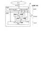
図4は、プロセッサ104により実現されるファームウェアの機能構成例を示すブロック図である。プロセッサ104により実現されるファームウェアの各機能は、大きく、データ管理部120、ATAコマンド処理部121、セキュリティ管理部122、ブートローダ123、初期化管理部124、デバッグサポート部125に分類される。 FIG. 4 is a block diagram illustrating a functional configuration example of firmware realized by the
データ管理部120は、NANDコントローラ112、第1のECC回路114を介して、NANDメモリ10−DRAM20間のデータ転送、NANDメモリ10に関する各種機能を制御する。ATAコマンド処理部121は、ATAコントローラ110、およびDRAMコントローラ113を介して、データ管理部120と協動してDRAM20−ホスト装置1間のデータ転送処理を行う。セキュリティ管理部122は、データ管理部120およびATAコマンド処理部121と協動して各種のセキュリティ情報を管理する。 The
ブートローダ123は、パワーオン時、各管理プログラム(ファームウェア)をNANDメモリ10からSRAM120にロードする。初期化管理部124は、ドライブ制御回路4内の各コントローラ/回路の初期化を行う。デバッグサポート部125は、外部からRS232Cインタフェースを介して供給されたデバッグ用データを処理する。主に、データ管理部120、ATAコマンド処理部121、およびセキュリティ管理部122が、SRAM114に記憶される各管理プログラムをプロセッサ104が実行することによって実現される機能部である。 The
本実施形態では、主としてデータ管理部120が実現する機能について説明する。データ管理部120は、ATAコマンド処理部121が記憶デバイスであるNANDメモリ10やDRAM20に対して要求する機能の提供(ホスト装置からのWrite要求、Cache Flush要求、Read要求等の各種コマンドへの応答)と、アドレス領域とNANDメモリ10との対応関係の管理および管理情報の保護と、DRAM10およびNANDメモリ10を利用した高速で効率の良いデータ読み出し/書き込み機能の提供、NANDメモリ10の信頼性の確保などを行う。 In the present embodiment, functions realized by the
図5は、NANDメモリ10およびDRAM20内に形成された機能ブロックを示すものである。ホスト1とNANDメモリ10との間には、DRAM20上に構成されたライトキャッシュ(WC)21およびリードキャッシュ(RC)22が介在している。WC21はホスト装置1からのWriteデータを一時保存し、RC22はNANDメモリ10からのReadデータを一時保存する。NANDメモリ10内の論理ブロックは、書き込み時のNANDメモリ10に対する消去の量を減らすために、データ管理部120により、前段ストレージ領域(FS:Front Storage)12、中段ストレージ領域(IS:Intermediate Storage)13およびメインストレージ領域(MS:Main Storage)11という各管理領域に割り当てられている。FS12は、WC21からのデータを「小さな単位」であるクラスタ単位に管理するものであり、小データを短期間保存する。IS13は、FS12から溢れたデータを「小さな単位」であるクラスタ単位に管理するものであり、小データを長期間保存する。MS11は、WC21、FS12、IS13からのデータを「大きな単位」であるトラック単位で長期間記憶する。例えば、記憶容量は、MS>IS、FS>WCの関係となる。 FIG. 5 shows functional blocks formed in the
小さな管理単位を、NANDメモリ10の記憶領域全てに適用すると、後述する管理テーブルのサイズが肥大化し、DRAM20に収まらないので、小さな管理単位で管理するのは、最近書き込まれたばかりのデータと、NANDメモリ10への書き込み効率が悪い小さなデータのみとするようにNANDメモリ10の各ストレージを構成している。 If a small management unit is applied to all the storage areas of the
図6は、WC21からNANDメモリ10への書き込み処理(WR処理)に係わるより詳細な機能ブロック図を示すものである。FS12の前段には、WC21からのデータをバッファリングするFSインプットバッファ(FSIB)12aが設けられている。また、MS11の前段には、WC21、FS12、またはIS13からのデータをバッファリングするMSインプットバッファ(MSIB)11aが設けられている。また、MS11には、トラック前段ストレージ領域(TFS)11bが設けられている。TFS11bは、MSIB11aとMS11の間に介在するFIFO(First in First out)構造を有するバッファであり、TFS11bに記録されたデータは、MSIB11aから直接MS11に書き込まれるデータよりも更新頻度が高いデータである。MS11、MSIB11a、TFS11b、FS12、FSIB12a、およびIS13には、NANDメモリ10内の各論理ブロックの何れかが割り当てられている。 FIG. 6 shows a more detailed functional block diagram related to the writing process (WR process) from the
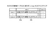
つぎに、図5、図6の各構成要素の具体的な機能構成について詳述する。ホスト装置1はSSD100対し、ReadまたはWriteする際には、ATAインタフェースを介して論理アドレスとしてのLBA(Logical Block Addressing)を入力する。LBAは、図7に示すように、セクタ(サイズ:512B)に対して0からの通し番号をつけた論理アドレスである。本実施の形態においては、図5の各構成要素であるWC21、RC22、FS12、IS13、MS11の管理単位として、LBAの下位(l−k+1)ビット目から上位のビット列で構成される論理クラスタアドレスと、LBAの下位(l−i+1)ビットから上位のビット列で構成される論理トラックアドレスとを定義する。1クラスタ=2(l−k)セクタで、1トラック=2(k−i)クラスタである。Next, specific functional configurations of the components shown in FIGS. 5 and 6 will be described in detail. When reading or writing to the
・リードキャッシュ(RC)22
RC22について説明する。RC22は、ATAコマンド処理部121からのRead要求に対して、NANDメモリ10(FS12、IS13、MS11)からのReadデータを一時的に保存するための領域である。RC22は、本実施形態では例えば、m-line、n-way(mは2(k−i)以上の自然数、nは2以上の自然数)セットアソシアティブ方式で管理されており、1エントリに1クラスタ分のデータを保持できる。論理クラスタアドレスのLSB(k−i)ビットでlineが決定される。なお、RC22は、フルアソシアティブ方式で管理されていても良いし、単純なFIFO方式で管理されていてもよい。Read cache (RC) 22
The
・ライトキャッシュ(WC)21
WC21について説明する。WC21は、ATAコマンド処理部121からのWrite要求に対して、ホスト装置1からのWriteデータを一時的に保存するための領域である。m-line、n-way(mは2(k−i)以上の自然数、nは2以上の自然数)セットアソシアティブ方式で管理されており、1エントリに1クラスタ分のデータを保持できる。論理クラスタアドレスのLSB(k−i)ビットでlineが決定される。例えば、way1〜waynの順で書き込み可能なwayが検索される。また、WC21に登録されているトラックは最も古く更新された順が分かるように後述するWCトラック管理テーブル24のFIFO構造によってLRU(Least Recently Used)で管理される。なお、WC21は、フルアソシアティブ方式で管理されていても良い。また、WC21は、RC22とline数、way数が互いに異なっていてもよい。-Write cache (WC) 21
The
Write要求により書き込まれたデータは、一旦WC21上に格納される。WC21からNANDメモリ10へ追い出すデータの決定方法は以下のルールに従う。
(i)タグによって決定されたlineの書き込み可能なwayが最後の(本実施形態では、n個目の)空きwayだった場合、則ち最後の空きwayが使用される場合は、そのlineに登録されたトラックのうち、LRUに基づいて最も古く更新されたトラックを追い出し確定する。
(ii)WC21に登録されている異なるトラックの個数が所定数を超えた場合、LRU順で、当該トラックに属するWC中のクラスタ数が所定数未満のトラックの追い出しを確定する。Data written by the Write request is temporarily stored on the
(I) When the writable way of the line determined by the tag is the last (in the present embodiment, nth) free way, that is, when the last free way is used, Of the registered tracks, the oldest updated track is checked out based on the LRU.
(Ii) When the number of different tracks registered in the
以上の方針で追い出すトラックを決定する。その際、追い出すのは同一トラックに含まれる全てのデータであり、追い出されるデータ量が、例えばトラックサイズの50%を超えていればMS11へ、超えていなければFS12へ追い出す。 The truck to be driven is determined according to the above policy. At that time, all the data included in the same track is evicted. If the amount of data evicted exceeds 50% of the track size, for example, it is evicted to MS11.
さらに(i)の条件でトラック追い出しが発生した場合で、MS11へ追い出す場合は、追い出されるトラック数が2i個(もともと2i個以上のときは2i+1個)になるまで、WC21内のトラックのうち上記追い出されるデータ量がトラックサイズの50%を超えるという条件を満たすトラックを上記(i)のポリシーで選択して追い出し候補に追加する。別言すれば、追い出されるトラックが2i個未満の場合、WC中のトラックの古いものから2i個になるまで、2(k−i−1)個以上有効クラスタをもつトラックを選択して追い出し候補に追加する。Further, when track eviction occurs under the condition (i) and when eviction to MS11, the tracks in WC21 until the number of eviction tracks is 2i (originally 2i + 1 when 2i or more). Of these, tracks that satisfy the condition that the amount of data to be evicted exceeds 50% of the track size are selected by the policy (i) and added to the evicting candidates. In other words, if there are less than 2i tracks to be evicted, select tracks with 2(k−i−1) or more valid clusters until there are 2i tracks from the oldest one in the WC. Add to eviction candidates.
また、(i)の条件でトラック追い出しが発生した場合で、FS12に追い出す場合は、追い出されるクラスタ数が2k個になるまでWC21内のトラックのうちLRU順に上記追い出されるデータ量がトラックサイズの50%未満であるという条件を満たすトラックを探してそのクラスタを追い出し候補に追加する。別言すれば、WC中のトラックを古い順に辿って2(k−i−1)個未満の有効クラスタしかもたないトラックからクラスタを取り出していき、有効クラスタ数が2(k−i−1)個になったら、それらクラスタをFSIB12aに論理ブロック単位で追い出しする。ただし、2(k−i−1)個見つからなかった場合は、FSIB12aに論理ページ単位で追い出しする。なお、FS12への追い出しを論理ブロック単位とするか、論理ページ単位とするかの有効クラスタ数の閾値は、2(k−i−1)個という1論理ブロック分の値にかぎるわけではなく、1論理ブロック分より若干少ない値であってもよい。Also, when track flush is performed under the conditions in, the data is flushed to the
また、ATAコマンド処理部121からのCache Flush要求では、WC21の内容が全て、上記と同じ条件(追い出されるデータ量がトラックサイズの50%を超えていればMS11へ、超えていなければFS12へ)で、FS12もしくはMS11に対して追い出される。 Also, in the Cache Flush request from the ATA command processing unit 121, all the contents of the
・前段ストレージ領域(FS)12
つぎに、FS12について説明する。FS12はクラスタ単位でデータを管理されるFIFOである。FS12は、ここを通過しているデータは、後段のIS13よりも更新頻度が高いとみなすためのバッファである。すなわち、FS12のFIFO構造においては、FIFO中を通過中の有効クラスタ(最新クラスタ)は、ホストからの同じアドレスに対する再書き込みがあった場合無効化されるので、FS12を通過中のクラスタは、FS12からIS13やMS11に追い出されたクラスタよりも、更新頻度が高いとみなすことができる。-Previous storage area (FS) 12
Next, the
FS12を設けることで、後段のIS13におけるコンパクション処理に更新頻度の高いデータが紛れ込む可能性を低減している。無効化によって古いクラスタを保持していた論理ブロック自体の持つ有効クラスタ数が0となった場合、その論理ブロックは開放され、フリーブロックFBに割り当てられる。また、論理ブロックが無効化された場合、新たなフリーブロックFBを取得し、FS12に割り当てる。 The provision of the
WC21からFS12に対してクラスタデータの移動が発生すると、そのクラスタはFSIB12aに割り当てられた論理ブロックに対して書き込まれる。FSIB12a中に全てのページの書き込みが完了したブロックが存在する場合、後述するCIB処理によってそれらのブロックはFSIB12aからFS12にMoveされる。このFSIB12aからFS12へのMoveの際に、FS12のブロック数がFS12として許容される所定の上限値を超えると、最も古いブロックがFS12からIS13またはMS11に追い出されることになる。例えば、トラック内の有効クラスタの割合が50%以上のトラックは、MS11(TFS11b)への書き込みを行い、有効クラスタが残ったブロックを、IS13へMoveする。 When movement of cluster data from the
NANDメモリ10内の構成要素間のデータ移動には、MoveとCopyの二通りがある。Moveは、後述する管理テーブルのポインタの付け替えを行うだけで、実際のデータの書き換えは行わない方法である。Copyは、一方の構成要素に格納されているデータを、ページ単位、トラック単位、ブロック単位で他方の構成要素に実際に書き換える方法である。 There are two types of data movement between components in the NAND memory 10: Move and Copy. Move is a method that does not rewrite actual data, only by changing pointers in a management table, which will be described later. Copy is a method of actually rewriting data stored in one component to the other component in page units, track units, or block units.
・中段ストレージ領域(IS)13
つぎに、IS13について説明する。IS13は、FS13と同様にクラスタ単位でデータの管理が行われる。前述したように、IS13に格納されたデータは、更新頻度が低いデータとみなすことができる。FS12からIS13に対して論理ブロックの移動(Move)、すなわちFS12からの追い出しが発生すると、以前FS12の管理対象であった追い出し対象の論理ブロックはポインタの付け替えによりIS13の管理対象ブロックとなる。このFS12からIS13への論理ブロックの移動により、IS13のブロック数がIS13として許容される所定の上限値を超えると、すなわちIS内の書き込み可能なフリーブロックFBの数が閾値を下回ると、IS13からMS11へのデータ追い出しおよびコンパクション処理が実行され、IS13のブロック数は規定値に戻される。-Middle storage area (IS) 13
Next, IS13 will be described. In the
IS13では、トラック内の有効クラスタ数を使って以下のような、追い出し処理およびコンパクション処理を、実行する。
・トラックをトラック内の有効クラスタ数×有効クラスタ係数(トラックがMS11内で無効トラックが存在する論理ブロックに存在するか否かによって重み付けされる数であり、存在したほうが存在しない場合より数が大きい)順にソートし、積の値が大きいトラック2i+1個(2論理ブロック分)を集めて論理ブロックサイズの自然数倍にしてMSIB11aに追い出す。
・有効クラスタ数が最も少ない2つの論理ブロックの合計有効クラスタ数が例えば、所定の設定値である2k個(1論理ブロック分)以上ある場合は、上のステップを繰り返す(IS内の2つの論理ブロックから、フリーブロックFBを作れるようになるまで行うため)。
・有効クラスタ数の少ない論理ブロックから順にクラスタを2k個集め、IS13内でコンパクションを行う。
なお、ここでは有効クラスタ数が最も少ない2つの論理ブロックを選択するとしたが、この数は2つに限定されず、2つ以上の数であればよい。また、所定の設定値は、選択する論路ブロック数よりも1つ少ない論理ブロック数に収容可能なクラスタ数以下であればよい。In IS13, the following eviction process and compaction process are executed using the number of valid clusters in the track.
Number of effective clusters in the track × effective cluster coefficient (the number is weighted depending on whether or not the track exists in the logical block where the invalid track exists in the
· The total number valid clusters smallest number two logical blocks is, for example, if 2k (for one logical block) or a predetermined set value, and repeats the above steps (the two in IS This is done until a free block FB can be created from the logical block).
Although the two logical blocks having the smallest number of valid clusters are selected here, this number is not limited to two and may be two or more. The predetermined set value may be equal to or less than the number of clusters that can be accommodated in the number of logical blocks one less than the number of logical block to be selected.
・メインストレージ領域(MS)11
つぎに、MS11について説明する。MS11はトラック単位でデータの管理を行う。MS11に格納されたデータは、更新頻度が低いとみなすことができる。WC21、FS12、IS13からMS11に対してトラックデータのCopyまたはMoveが発生すると、そのトラックはMSIS11aに割り当てられた論理ブロックに対して書き込まれる。一方で、トラック中の一部のデータ(クラスタ)のみがWC等から書き込まれるような場合には、既存のMS中のトラックデータと新しいデータをマージして新しいトラックデータを作った上でMSIB11aに書き込む、後述する受動マージが行われる。MS11内に無効トラックが蓄積し、MS11に割り当てられている論理ブロックの個数がMS11として許容されるブロック数の上限値を越えるような状況が発生すると、コンパクション処理を行って、無効なフリーブロックFBを作る。Main storage area (MS) 11
Next, the
MS11のコンパクション処理は、例えば、論理ブロック内の有効トラック数のみに注目した以下の方法を実施する。
・有効トラックが少ない論理ブロックから順番に、無効トラックを合わせることによって無効なフリーブロックFBが作れるようになるまで選択する。
・選択した論理ブロックに収容されたトラックを、WC21、FS12、IS13内のデータと統合する受動マージを行いながらコンパクションを実行する。
・2iトラック統合できた論理ブロックは、TFS11bに出力し(2iトラックMSコンパクション)、2iトラックに満たない個数のトラックは、MSIB11aに出力して(2iトラック未満コンパクション)、より多くの無効なフリーブロックFBを作る。For the compaction processing of the
Select in order from logical blocks with few valid tracks until invalid free blocks FB can be created by combining invalid tracks.
Compaction is performed while performing passive merging to integrate tracks contained in the selected logical block with data in the WC21, FS12, and IS13.
-2i track integrated logical block is output to
TFS11bは、トラック単位でデータを管理されるFIFOである。TFS11bは、ここを通過しているデータは、後段のMS11よりも更新頻度が高いとみなすためのバッファである。すなわち、TFS11bのFIFO構造においては、FIFO中を通過中の有効トラック(最新トラック)は、ホストからの同じアドレスに対する再書き込みがあった場合無効化されるので、TFS11bを通過中のトラックは、TFS11bからMS11に追い出されたトラックよりも、更新頻度が高いとみなすことができる。 The
図8は、データ管理部120が図5および図6に示した各構成要素を制御管理するための管理テーブルを示すものである。データ管理部120は、前述したように、ATAコマンド処理部121とNANDメモリ10とをブリッジする機能を有し、DRAM20に記憶したデータの管理を行うDRAM層管理部120aと、NANDメモリ10に記憶したデータの管理を行う論理NAND層管理部120bと、NANDメモリ10を物理記憶デバイスとして管理する物理NAND層管理部120cとから構成される。RCクラスタ管理テーブル23、WCトラック管理テーブル24、WCクラスタ管理テーブル25は、DRAM層管理部120aにより制御される。トラック管理テーブル30、FS/IS管理テーブル40、MS論理ブロック管理テーブル35、FS/IS論理ブロック管理テーブル42、FS/IS内クラスタ管理テーブル44は、論理NAND層管理部120bにより管理される。論物変換テーブル50は、物理NAND層管理部120cにより管理される。 FIG. 8 shows a management table for the
RC22は、逆引きテーブルであるRCクラスタ管理テーブル23によって管理される。逆引きテーブルでは、記憶デバイスの位置からその位置に記憶されている論理アドレスを検索することができる。WC21は、逆引きテーブルであるWCクラスタ管理テーブル25および正引きテーブルであるWCトラック管理テーブル24によって管理される。正引きテーブルでは、論理アドレスからその論理アドレスに対応するデータが存在する記憶デバイス位置を検索することができる。 The
NANDメモリ10内のFS12(FSIB12a)、IS13、MS11(TFS11b、MSIB11a)は、トラック管理テーブル30、FS/IS管理テーブル40、MS論理ブロック管理テーブル35、FS/IS論理ブロック管理テーブル42、FS/IS内クラスタ管理テーブル44によってその論理アドレスが管理される。また、NANDメモリ10内のFS12(FSIB12a)、IS13、MS11(TFS11b、MSIB11a)は、論物変換テーブル50によって論理アドレスと物理アドレスとの変換が行われる。これらの各管理テーブルは、NANDメモリ10上の領域に記憶されており、SSD100の初期化時にNANDメモリ10からDRAM20上に読み込まれて、使用される。 The FS12 (FSIB12a), IS13, and MS11 (TFS11b, MSIB11a) in the
・RCクラスタ管理テーブル23(逆引き)
まず、図9を用いてRCクラスタ管理テーブル23について説明する。RC22は、前述したように、論理クラスタアドレスLSB(k−i)ビットでインデックスされるn-wayセットアソシアティブ方式で管理されている。RCクラスタ管理テーブル23は、RC(クラスタサイズ×m-line×n-way)22の各エントリのタグを管理するためのテーブルであり、各タグは、複数ビットの状態フラグ23aと、論理トラックアドレス23bによって構成されている。状態フラグ23aには、当該エントリを使用しても良いか否か(有効/無効)を示すValidビットの他に、当該エントリがNANDメモリ10からの読み出し待ちか否かを示すビット、当該エントリがATAコマンド処理部121への読み出し待ちか否かを示すビットなどが含まれる。RCクラスタ管理テーブル23は、DRAM20上のタグ記憶位置からLBAに一致する論理トラックアドレスを検索する逆引きテーブルとして機能する。RC cluster management table 23 (reverse lookup)
First, the RC cluster management table 23 will be described with reference to FIG. As described above, the
・WCクラスタ管理テーブル25(逆引き)
つぎに、図10を用いてWCクラスタ管理テーブル25について説明する。WC21は、前述したように、論理クラスタアドレスLSB(k−i)ビットでインデックスされるn-wayセットアソシアティブ方式で管理されている。WCクラスタ管理テーブル25は、WC(クラスタサイズ×m-line×n-way)21の各エントリのタグを管理するためのテーブルであり、各タグは、複数ビットの状態フラグ25aと、セクタ位置ビットマップ25bと、論理トラックアドレス25cによって構成されている。WC cluster management table 25 (reverse lookup)
Next, the WC cluster management table 25 will be described with reference to FIG. As described above, the
状態フラグ25aには、当該エントリを使用しても良いか否か(有効/無効)を示すValidビットの他に、当該エントリがNANDメモリ10への追い出し待ちか否かを示すビット、当該エントリがATAコマンド処理部からの書き込み待ちか否かを示すビットなどが含まれる。セクタ位置ビットマップ25bは、1クラスタに含まれる2(l−k)セクタのうちのどのセクタに有効なデータを保持しているかを2(l−k)ビットに展開して示すものである。このセクタ位置ビットマップ25bによって、WC21において、LBAと同じセクタ単位の管理を行うことができる。WCクラスタ管理テーブル25は、DRAM20上のタグ記憶位置からLBAに一致する論理トラックアドレスを検索する逆引きテーブルとして機能する。In the
・WCトラック管理テーブル24(正引き)
つぎに、図11を用いてWCトラック管理テーブル24について説明する。WCトラック管理テーブル24は、WC21上に格納されているクラスタをトラック単位でまとめた情報を管理するものであり、FIFO的な機能を有するリンクドリスト構造によってトラック間のWC21に登録された順序(LRU)を表現している。なお、WC21で最後に更新された順序によってLRUを表現するようにしてもよい。各リストのエントリは、論理トラックアドレス24a、当該論理トラックアドレスに含まれるWC21中の有効クラスタ数24b、way-lineビットマップ24cおよび次のエントリへのポインタを示すnextポインタ24dから構成されている。WCトラック管理テーブル24は、論理トラックアドレス24aから所要情報を得るので、正引きテーブルとして機能する。WC track management table 24 (forward lookup)
Next, the WC track management table 24 will be described with reference to FIG. The WC track management table 24 manages information in which the clusters stored on the
way-lineビットマップ24cは、WC21中で当該論理トラックアドレスに含まれる有効クラスタがWC21中のm×nのエントリ中のどのエントリに格納されているか示すマップ情報であり、有効クラスタが格納されているエントリではValidビットが”1”になっている。このway-lineビットマップ24cは、例えば、(1ビット(Valid)+log2nビット(n-way))×mビット(m-line)で構成されている。WCトラック管理テーブル24はリンクドリスト構造を有しており、WC21中に存在する論理トラックアドレスに関する情報のみがエントリされている。The way-
・トラック管理テーブル30(正引き)
つぎに、図12を用いてトラック管理テーブル30について説明する。トラック管理テーブル30は、論理トラックアドレス単位でMS11上の論理的なデータ位置を管理するためのテーブルであり、クラスタ単位でFS12やIS13にデータが保持されている場合には、それらに関する基本情報と、詳細情報へのポインタも保持している。論理トラックアドレス30aをインデックスとした配列形式で構成される。論理トラックアドレス30aをインデックスとした各エントリは、クラスタビットマップ30b、論理ブロックID30c+論理ブロック内トラック位置30d、クラスタテーブルポインタ30e、FSクラスタ数30f、ISクラスタ数30gなどの情報で構成されている。トラック管理テーブル30は、論理トラックアドレスをインデックスとして、その論理トラックアドレスに対応する論理トラックが記憶されている論理ブロックID(記憶デバイス位置に対応)などの所要情報を得るので、正引きテーブルとして機能する。・ Track management table 30 (forward lookup)
Next, the track management table 30 will be described with reference to FIG. The track management table 30 is a table for managing logical data positions on the
クラスタビットマップ30bは、1つの論理トラックアドレス範囲に属する2(k−i)個のクラスタをクラスタアドレス昇順に例えば8分割したビットマップであり、8個の各ビットは、2(k−i−3)個のクラスタアドレスに対応するクラスタがMS11に存在するか、FS12もしくはIS13に存在するかを示している。ビットが“0”の場合は、その検索対象のクラスタは確実にMS11内に存在することを示し、ビットが“1”の場合は、そのクラスタはFS12もしくはIS13に存在する可能性があることを示している。The
論理ブロックID30cは、当該論理トラックアドレスに対応する論理トラックが記憶されている論理ブロックIDを識別するための情報である。論理ブロック内トラック位置30dは、論理ブロックID30cで指定された論理ブロック中における当該論理トラックアドレス(30a)に対応するトラックの記憶位置を示すものである。1論理ブロックは最大2i個の有効トラックで構成されるので、論理ブロック内トラック位置30dは、iビットで2i個のトラック位置を識別する。The
クラスタテーブルポインタ30eは、リンクドリスト構造を有するFS/IS管理テーブル40の各リストの先頭エントリへのポインタである。クラスタビットマップ30bの検索で、当該クラスタがFS12/IS13に存在する可能性があることを示していた場合、クラスタテーブルポインタ30eを用いてFS/IS管理テーブル40の検索を実行する。FSクラスタ数30fは、FS12内に存在する有効クラスタ数を示している。ISクラスタ数30gは、IS13内に存在する有効クラスタ数を示している。 The
・FS/IS管理テーブル40(正引き)
つぎに、図13を用いてFS/IS管理テーブル40について説明する。FS/IS管理テーブル40は、論理クラスタ単位でFS12(FSIB12aも含む)もしくはIS13に保持されているデータの位置を管理するためのテーブルである。図13に示すように、論理トラックアドレス毎に独立したリンクドリスト形式で構成され、各リストの先頭エントリへのポインタは、前述したように、トラック管理テーブル30のクラスタテーブルポインタ30eのフィールドに保持されている。図13では、2つの論理トラックアドレス分のリンクドリストが示されている。各エントリは、論理クラスタアドレス40a、論理ブロックID40b、論理ブロック内クラスタ位置40c、FS/ISブロックID40d、nextポインタ40eから構成されている。FS/IS管理テーブル40は、論理クラスタアドレス40aから、その論理クラスタアドレスに対応する論理クラスタが記憶されている論理ブロックID40b、論理ブロックン内クラスタ位置40c(記憶デバイス位置に対応)などの所要情報を得るので、正引きテーブルとして機能する。FS / IS management table 40 (forward lookup)
Next, the FS / IS management table 40 will be described with reference to FIG. The FS / IS management table 40 is a table for managing the location of data held in the FS 12 (including the
論理ブロックID40bは、当該論理クラスタアドレス40aに対応する論理クラスタが記憶されている論理ブロックIDを識別するための情報である。論理ブロック内クラスタ位置40cは、論理ブロックID40bで指定された論理ブロック中における当該論理クラスタアドレス40aに対応するクラスタの記憶位置を示すものである。1論理ブロックは最大2k個の有効クラスタで構成されるので、論理ブロック内クラスタ位置40cは、kビットで2k位置を識別する。FS/ISブロックID40dは、後述するFS/IS論理ブロック管理テーブル42のインデックスであるFS/ISブロックIDが登録されている。FS/ISブロックIDは、FS12またはIS13に所属する論理ブロックを識別するための情報であり、このFS/IS管理テーブル40でのFS/ISブロックID40dは、後述するFS/IS論理ブロック管理テーブル42とのリンクのために登録されている。nextポインタ40eは、論理トラックアドレス毎にリンクされる同じリスト内の次のエントリへのポインタを示している。The
・MS論理ブロック管理テーブル35(逆引き)
つぎに、図14を用いてMS論理ブロック管理テーブル35について説明する。MS論理ブロック管理テーブル35は、MS11に用いられている論理ブロックに関する情報(どの論理トラックが記憶されているか、追記可能か等)を一元管理するためのテーブルである。なお、MS論理ブロック管理テーブル35には、FS12(FSIB12も含む)、IS13に所属する論理ブロックに関する情報も登録されている。MS論理ブロック管理テーブル35は、論理ブロックID35aをインデックスとした配列形式で構成され、エントリ数は128GBのNANDメモリ10の場合は、32Kエントリまで持つことができる。各エントリは、2iトラック分のトラック管理ポインタ35b、有効トラック数35c、書き込み可能先頭トラック35d、Validフラグ35eから構成されている。このMS論理ブロック管理テーブル35は、記憶デバイス位置に対応する論理ブロックID35aから、この論理ブロックに記憶されている論理トラックアドレスなどの所要情報を得るので、逆引きテーブルとして機能する。MS logical block management table 35 (reverse lookup)
Next, the MS logical block management table 35 will be described with reference to FIG. The MS logical block management table 35 is a table for centrally managing information on logical blocks used in the MS 11 (which logical track is stored, whether additional recording is possible, etc.). In the MS logical block management table 35, information on logical blocks belonging to FS12 (including FSIB12) and IS13 is also registered. The MS logical block management table 35 is configured in an array format using the
トラック管理ポインタ35bは、論理ブロックID35aで指定される当該論理ブロック内の2i個のトラック位置毎に対応する論理トラックアドレスを保持する。この論理トラックアドレスを用いて、論理トラックアドレスをインデックスとするトラック管理テーブル30を検索することができる。有効トラック数35cは、論理ブロックID35aで指定される当該論理ブロックに記憶されているトラックのうちの有効なものの個数(最大2i個)を示している。書き込み可能先頭トラック位置35dは、論理ブロックID35aで指定される当該論理ブロックが追記中のブロックであった場合における追記可能なトラック先頭位置(0〜2i−1、追記終了時は2i)を示している。Validフラグ35eは、当該論理ブロックエントリがMS11(MSIB11aも含む)として管理されている場合に“1”である。The
・FS/IS論理ブロック管理テーブル42(逆引き)
つぎに、図15を用いてFS/IS論理ブロック管理テーブル42について説明する。FS/IS論理ブロック管理テーブル42は、FS/ISブロックID42aをインデックスとした配列形式で構成され、FS12またはIS13として利用されている論理ブロックに関する情報(論理ブロックIDとの対応、FS/IS内クラスタ管理テーブル44へのインデックス、追記可能か等)を管理するためのテーブルである。FS/IS論理ブロック管理テーブル42は、主にFS/IS管理テーブル40中のFS/ISブロックID40dを用いてアクセスされる。各エントリは、論理ブロックID42b、ブロック内クラスタテーブル42c、有効クラスタ数42d、書き込み可能先頭ページ42e、Validフラグ42fから構成されている。このMS論理ブロック管理テーブル35は、記憶デバイス位置に対応するFS/ISブロックID42aから、この論理ブロックに記憶されている論理クラスタなどの所要情報を得るので、逆引きテーブルとして機能する。FS / IS logical block management table 42 (reverse lookup)
Next, the FS / IS logical block management table 42 will be described with reference to FIG. The FS / IS logical block management table 42 is configured in an array format using the FS /
論理ブロックID42bには、MS論理ブロック管理テーブル35に登録された論理ブロックの中で、FS12(FSIB12も含む)、IS13に所属している論理ブロックに対応する論理ブロックIDが登録される。ブロック内クラスタテーブル42cには、論理ブロック中の各クラスタ位置にどの論理クラスタアドレスで指定される論理クラスタが記録されているかを示す後述するFS/IS内クラスタ管理テーブル44へのインデックスが登録される。有効クラスタ数42dは、FS/ISブロックID42aで指定される当該論理ブロックに記憶されているクラスタのうちの有効なものの個数(最大2k個)を示している。書き込み可能先頭ページ位置42eは、FS/ISブロックID42aで指定される当該論理ブロックが追記中のブロックであった場合における追記可能な先頭ページ位置(0〜2j−1、追記終了時は2i)を示している。Validフラグ42fは、この論理ブロックエントリがFS12(FSIB12も含む)またはIS13として管理されている場合に“1”である。Among the logical blocks registered in the MS logical block management table 35, the
・FS/IS内クラスタ管理テーブル44(逆引き)
つぎに、図16を用いてFS/IS内クラスタ管理テーブル44について説明する。FS/IS内クラスタ管理テーブル44は、FS12もしくはIS13として利用されている論理ブロック中の各クラスタ位置にどの論理クラスタが記録されているのかを示すテーブルである。1論理ブロックあたり、2jページ×2(k−j)クラスタ=2k個のエントリを持ち、当該論理ブロック内のクラスタ位置の0番目〜2k−1番目に対応する情報が連続領域に配置される。さらにこの2k個の情報を含むテーブルがFS12およびIS13に所属する論理ブロック数(P個)分だけ保持されており、FS/IS論理ブロック管理テーブル42のブロック内クラスタテーブル42cは、このP個のテーブルに対する位置情報(ポインタ)となっている。連続領域に配される各エントリ44aの位置は、1論理ブロック中のクラスタ位置を示し、また各エントリ44aの内容は、当該クラスタ位置にどの論理クラスタが記憶されているかが識別できるように、FS/IS管理テーブル40で管理される該当論理クラスタアドレスを含むリストへのポインタが登録されている。すなわち、エントリ44aは、リンクドリストの先頭を指し示すのではなく、リンクドリスト中の該当論理クラスタアドレスを含む1つのリストへのポインタが登録されている。-FS / IS cluster management table 44 (reverse lookup)
Next, the FS / IS intra-cluster management table 44 will be described with reference to FIG. The FS / IS intra-cluster management table 44 is a table showing which logical cluster is recorded at each cluster position in the logical block used as the
・論物変換テーブル50(正引き)
つぎに、図17を用いて論物変換テーブル50について説明する。論物変換テーブル50は、論理ブロックID50aをインデックスとした配列形式で構成され、エントリ数は、128GBのNANDメモリ10の場合は、最大32Kエントリまで持つことができる。論物変換テーブル50は、論理ブロックIDと物理ブロックIDとの変換、寿命に関する情報を管理するためのテーブルである。各エントリは、物理ブロックアドレス50b、消去回数50c、読み出し回数50dから構成される。この論物変換テーブル50は、論理ブロックIDから物理ブロックID(物理ブロックアドレス)などの所要情報を得るので、正引きテーブルとして機能する。・ Conversion table 50 (forward lookup)
Next, the logical-physical conversion table 50 will be described with reference to FIG. The logical-physical conversion table 50 is configured in an array format using the
物理ブロックアドレス50bは、1つの論理ブロックID50aに所属する8個の物理ブロックID(物理ブロックアドレス)を示している。消去回数50cは、当該論理ブロックIDの消去回数を示している。バッドブロック(BB)管理は、物理ブロック(512KB)単位に行われるが、消去回数の管理は、32ビット倍速モードによる1論理ブロック(4MB)単位に管理される。読み出し回数50dは、当該論理ブロックIDの読み出し回数を示している。消去回数50cは、例えば、NAND型フラッシュメモリの書き換え回数を平準化するウェアレベリング処理で利用することが可能である。読み出し回数50dは、リテンション特性の劣化した物理ブロックに保持されるデータの再書き込みを行うリフレッシュ処理で利用することが可能である。 The
図8に示した管理テーブルを管理対象毎にまとめると次のようになる。
RC管理:RCクラスタ管理テーブル
WC管理:WCクラスタ管理テーブル、WCトラック管理テーブル
MS管理:トラック管理テーブル30、MS論理ブロック管理テーブル35
FS/IS管理:トラック管理テーブル30、FS/IS管理テーブル40、MS論理ブロック管理テーブル35、FS/IS論理ブロック管理テーブル42、FS/IS内クラスタ管理テーブル44The management table shown in FIG. 8 is summarized for each management target as follows.
RC management: RC cluster management table WC management: WC cluster management table, WC track management table MS management: track management table 30, MS logical block management table 35
FS / IS management: track management table 30, FS / IS management table 40, MS logical block management table 35, FS / IS logical block management table 42, FS / IS intra-cluster management table 44
なお、MS構造管理テーブル(図示せず)において、MS11,MSIB11a、TFS11bを含めたMS領域の構造を管理しており、具体的には、MS11、MSIB11a、TFS11bに割り当てた論理ブロックなどを管理している。また、FS/IS構造管理テーブル(図示せず)において、FS12、FSIB12a、IS13を含めたFS/IS領域の構造を管理しており、具体的には、FS12、FSIB12a、IS13に割り当てた論理ブロックなどを管理している。 The MS structure management table (not shown) manages the structure of the MS area including MS11, MSIB11a, and TFS11b. Specifically, it manages logical blocks assigned to MS11, MSIB11a, and TFS11b. ing. In addition, in the FS / IS structure management table (not shown), the structure of the FS / IS area including FS12, FSIB12a, and IS13 is managed. Specifically, logical blocks allocated to FS12, FSIB12a, and IS13 I manage.
・Read処理
つぎに、図18に示すフローチャートを参照して、読み出し処理について説明する。ATAコマンド処理部121から、Readコマンドおよび読み出しアドレスとしてのLBAが入力されると、データ管理部120は、図9に示したRCクラスタ管理テーブル23と図10に示したWCクラスタ管理テーブル25を検索する(ステップS100)。具体的には、LBAのクラスタアドレスのLSB(k−i)ビット(図7参照)に対応するlineをRCクラスタ管理テーブル23とWCクラスタ管理テーブル25から選択し、選択したlineの各wayにエントリされている論理トラックアドレス23b、25cをLBAのトラックアドレスと比較し(ステップS110)、一致したwayが存在している場合は、キャッシュヒットとし、ヒットしたRCクラスタ管理テーブル23またはWCクラスタ管理テーブル25の該当line、該当wayに対応するWC21またはRC22のデータを読み出して、ATAコマンド処理部121に送る(ステップS115)。Read Process Next, the read process will be described with reference to the flowchart shown in FIG. When the Read command and the LBA as the read address are input from the ATA command processing unit 121, the
データ管理部120は、RC22またはWC21でヒットしなかった場合は(ステップS110)、検索対象のクラスタがNANDメモリ10のどこに格納されているかを検索する。データ管理部120は、まず、図12に示したトラック管理テーブル30を検索する(ステップS120)。トラック管理テーブル30は、論理トラックアドレス30aでインデックスされているため、LBAで指定された論理トラックアドレスに一致する論理トラックアドレス30aのエントリだけをチェックする。 If the
まず、チェックしたいLBAの論理クラスタアドレスに基づいてクラスタビットマップ30bから対応するビットを選択する。対応するビットが“0”を示していれば、そのクラスタは確実にMS内に最新のデータが存在していることを意味する(ステップS130)。この場合は、このトラックが存在する論理ブロックIDおよびトラック位置を、同じ論理トラックアドレス30aのエントリ中の論理ブロックID30cと論理ブロック内トラック位置30dから得て、さらにLBAのクラスタアドレスのLSB(k−i)ビットを利用して、トラック位置からのオフセットを算出することで、NANDメモリ10内の当該クラスタアドレスに対応するクラスタデータが格納されている位置を算出することができる。具体的には、論理NAND層管理部120bでは、上記のようにしてトラック管理テーブル30から取得した論理ブロックID30cと論理ブロック内トラック位置30dと、LBAの論理クラスタアドレスのLSB(k−i)ビットを物理NAND層管理部120cに与える。 First, the corresponding bit is selected from the
物理NAND層管理部120cでは、論理ブロックID30cに対応する物理ブロックアドレス(物理ブロックID)を、論理ブロックIDをインデックスとしている図17に示す論物変換テーブル50から取得し(ステップS160)、さらに取得した物理ブロックID中のトラック位置(トラック先頭位置)を論理ブロック内トラック位置30dから算出し、さらにLBAのクラスタアドレスのLSB(k−i)ビットから、前記算出した物理ブロックID中のトラック先頭位置からのオフセットを算出することで、物理ブロック中のクラスタデータを取得することができる。NANDメモリ10のMS11から取得されたクラスタデータは、RC22を介してATAコマンド処理部121に送られる(ステップS180)。 In the physical NAND
一方、LBAのクラスタアドレスに基づくクラスタビットマップ30bの検索で、対応するビットが“1”を示していた場合は、そのクラスタがFS12またはIS13に格納されている可能性がある(ステップS130)。この場合は、トラック管理テーブル30の該当する論理トラックアドレス30aのエントリ中のクラスタテーブルポインタ30eのエントリを取り出し、このポインタを用いてFS/IS管理テーブル40の該当する論理トラックアドレスに対応するリンクドリストを順次検索する(ステップS140)。具体的には、該当する論理トラックアドレスのリンクドリスト中のLBAの論理クラスタアドレスに一致する論理クラスタアドレス40aのエントリを検索し、一致する論理クラスタアドレス40aのエントリが存在した場合は(ステップS150)、一致したリスト中の論理ブロックID40bおよび論理ブロック内クラスタ位置40cを取得し、前述と同様にして、論物変換テーブル50を用いて物理ブロック中のクラスタデータを取得する(ステップS160、S180)。具体的には、取得した論理ブロックIDに対応する物理ブロックアドレス(物理ブロックID)を、論物変換テーブル50から取得し(ステップS160)、さらに取得した物理ブロックID中のクラスタ位置を、論理ブロック内クラスタ位置40cのエントリから取得した論理ブロック内クラスタ位置から算出することで、物理ブロック中のクラスタデータを取得することができる。NANDメモリ10のFS12またはIS13から取得されたクラスタデータは、RC22を介してATAコマンド処理部121に送られる(ステップS180)。 On the other hand, if the corresponding bit indicates “1” in the search of the
このFS/IS管理テーブル40の検索によって、検索対象のクラスタが存在しなかった場合は(ステップS150)、再度トラック管理テーブル30のエントリを検索してMS11上の位置を確定する(ステップS170)。 If there is no cluster to be searched by searching the FS / IS management table 40 (step S150), the entry in the track management table 30 is searched again to determine the position on the MS 11 (step S170).
・Write処理
つぎに、図19に示すフローチャートを参照して、書き込み処理について説明する。FUA(DRAMキャッシュをバイパスしてNANDへの直接書き込みを行う)でないWriteコマンドにより書き込まれたデータは必ず一旦WC21上に格納され、その後条件に応じてNANDメモリ10に対して書き込まれることになる。書き込み処理では、追い出し処理、コンパクション処理が発生する可能性がある。この実施の形態では、書き込み処理を、ライトキャッシュフラッシュ処理(以下WCF処理)と、クリーンインプットバッファ処理(以下CIB処理)との2ステージに大きく分割している。ステップS300からステップS320までは、ATAコマンド処理部121からのWrite要求からWCF処理までを示しており、ステップS330〜最終ステップまでがCIB処理を示している。Write Process Next, the write process will be described with reference to the flowchart shown in FIG. Data written by a Write command other than FUA (bypassing the DRAM cache and performing direct writing to the NAND) is always stored once on the
WCF処理は、WC21にあるデータをNANDメモリ10(FS12のFSIB12aまたはMS11のMSIB11a)にcopyする処理であり、ATAコマンド処理部121からのWrite要求もしくはCache Flush要求単体は、この処理のみで完結することができる。これにより処理が開始されたATAコマンド処理部121のWrite要求の処理遅延を最大でもWC21の容量分のNANDメモリ10への書き込み時間に限定することができるようになる。 The WCF process is a process of copying data in the
CIB処理は、WCF処理によって書き込まれたFSIB12aのデータをFS12にMoveする処理と、WCF処理によって書き込まれたMSIB11aのデータをMS11にMoveする処理とを含む。CIB処理を開始すると、連鎖的にNANDメモリ10内の各構成要素(FS12、IS13、MS11など)間のデータ移動やコンパクション処理が発生する可能性があり、処理全体に要する時間は状態によって大きく変化する。 The CIB process includes a process of moving the data of the
まず、WCF処理の詳細について説明する。ATAコマンド処理部121から、Writeコマンドおよび書き込みアドレスとしてのLBAが入力されると、DRAM層管理部120は、図10に示したWCクラスタ管理テーブル25を検索する(ステップS300,S305)。WC21の状態は、図10に示したWCクラスタ管理テーブル25の状態フラグ25a(例えば3ビット)によって規定されている。状態フラグ25aは、最も典型的には、Invalid(使用可能)→ATAからの書き込み待ち→Valid(使用不可)→NANDへの追い出し待ち→Invalid(使用可能)という順に状態が遷移していく。まず、LBAのクラスタアドレスLSB(k−i)ビットから書き込み先のlineを決定し、決定したlineのn個のwayを検索する。決定したlineのn個のway中に、入力されたLBAと同じ論理トラックアドレス25cが格納されている場合は(ステップS305)、このエントリに上書きするのでこのエントリをクラスタ書き込み用に確保する(Valid(使用不可)→ATAからの書き込み待ち)。 First, details of the WCF processing will be described. When a Write command and an LBA as a write address are input from the ATA command processing unit 121, the DRAM
そして、DRAM層管理部120aは、該当エントリに対応するDRAMアドレスをATAコマンド処理部121に通知する。ATAコマンド処理部121による書き込みが終了すると、WCクラスタ管理テーブル25の該当エントリの状態フラグ25aをValid(使用不可)にし、さらにセクタ位置ビットマップ25bおよび論理トラックアドレス25cの欄に所要のデータを登録する。また、WCトラック管理テーブル24を更新する。具体的には、WCトラック管理テーブル24の各リスト中に既に登録済みの論理トラックアドレス24aと同じLBAアドレスが入力された場合は、該当するリストのWCクラスタ数24b、way−lineビットマップ24cを更新するとともに、当該リストが最新のリストとなるようにnextポインタ24dを変更する。また、WCトラック管理テーブル24の各リスト中に登録済みの論理トラックアドレス24aと異なるLBAアドレスが入力された場合は、新たに新しい論理トラックアドレス24a、WCクラスタ数24b、way−lineビットマップ24c、nextポインタ24dの各エントリを有するリストを作成し、最新のリストとして登録する。以上のようなテーブル更新を行って、書き込み処理が完了する(ステップS320)。 Then, the DRAM
一方、決定したlineのn個のway中に、入力されたLBAと同じ論理トラックアドレス25cが格納されていない場合は、NANDメモリへの追い出しが必要であるか否かを判断する(ステップS305)。すなわち、まず、決定したline中の書き込み可能なwayが最後のn個目のwayであるか否かを判断する。書き込み可能なwayとは、Invalid(使用可能)の状態フラグ25aをもつwayかあるいはValid(使用不可)でかつNANDへの追い出し待ちの状態フラグ25aを持つwayである。状態フラグ25aが、NANDへの追い出し待ちであるとは、追い出しが開始されて追い出しの終了待ちであることを意味する。そして、書き込み可能なwayが最後のn個目のwayでない場合であって、かつ書き込み可能なwayが、Invalid(使用可能)の状態フラグ25aをもつwayである場合は、このエントリをクラスタ書き込み用に確保する(Invalid(使用可能)→ATAからの書き込み待ち)。そして、該当エントリに対応するDRAMアドレスをATAコマンド処理部121に通知し、ATAコマンド処理部121によって書き込みを実行させる。そして、前記同様、WCクラスタ管理テーブル25およびWCトラック管理テーブル24を更新する(ステップS320)。 On the other hand, when the same
また、書き込み可能なwayが最後のn個目のwayでない場合であって、かつ書き込み可能なwayが、Valid(使用不可)でかつNANDへの追い出し待ちの状態フラグ25aを持つwayである場合は、このエントリをクラスタ書き込み用に確保する(Valid(使用不可)でかつNANDへの追い出し待ち→Valid(使用不可)でかつNANDへの追い出し待ちかつATAからの書き込み待ち)。そして、追い出しが終了すると、状態フラグ25aをATAからの書き込み待ちにし、さらに、該当エントリに対応するDRAMアドレスをATAコマンド処理部121に通知し、ATAコマンド処理部121によって書き込みを実行させる。そして、前記同様、WCクラスタ管理テーブル25およびWCトラック管理テーブル24を更新する(ステップS320)。 When the writable way is not the last nth way and the writable way is Valid (unusable) and has a
以上の処理は、ATAコマンド処理部121からからの書き込み要求が入力された際に、追い出し処理をトリガしなくてもよい場合である。一方、この後の説明は、書き込み要求が入力された時点後に、追い出し処理をトリガする場合である。ステップS305において、決定したline中の書き込み可能なwayが最後のn個目のwayである場合は、前述したWC21からNANDメモリ10へ追い出すデータの決定方法の(i)の箇所で説明した条件、すなわち、
(i) タグによって決定されたlineの書き込み可能なwayが最後の(本実施形態では、n個目の)空きwayだった場合、則ち最後の空きwayが使用される場合は、そのlineに登録されたトラックのうちLRUに基づいて最も古く更新されたトラックを追い出し確定する
に基づいて追い出すトラックすなわちWC21内エントリを選択する。The above process is a case where the eviction process need not be triggered when a write request from the ATA command processing unit 121 is input. On the other hand, the following description is a case in which the eviction process is triggered after a write request is input. In step S305, when the writable way in the determined line is the last nth way, the condition described in the section (i) of the method for determining the data to be expelled from the
(I) If the writable way of the line determined by the tag is the last (in this embodiment, the nth) free way, that is, if the last free way is used, A track to be driven out, that is, an entry in the
DRAM層管理部120aは、以上の方針で追い出すトラックを決定すると、前述したように、その際追い出すのは同一トラックに含まれるWC21中の全クラスタであり、追い出されるクラスタ量がトラックサイズの50%を超えていれば、すなわち追い出し確定トラックのうちWC中に有効クラスタ数が2(k−i−1)個以上ある場合は、MSIB11aへ追い出しを行い(ステップS310)、超えていなければ、すなわち追い出し確定トラックのうちWC中に有効クラスタ数が2(k−i−1)個未満である場合は、FSIB12aへと追い出す(ステップS315)。WC21からMSIB11aへの追い出し、WC21からFSIB12aへの追い出しの詳細は、後述する。選択された追い出しエントリの状態フラグ25aは、Valid(使用不可)からNANDメモリ10への追い出し待ちに移行される。When the DRAM
この追い出し先の判定は、WCトラック管理テーブル24を用いて実行される。すなわち、WCトラック管理テーブル24には、論理トラックアドレス毎に、有効なクラスタ数を示すWCクラスタ数24bのエントリが登録されており、このWCクラスタ数24bのエントリを参照することでWC21からの追い出し先を、FSIB12a、MSIB11aの何れにするかを決定する。また、way−lineビットマップ24cに、当該論理トラックアドレスに所属する全てのクラスタがビットマップ形式で登録されているので、追い出しを行う際には、このway−lineビットマップ24cを参照することで、容易に、追い出すべき各クラスタのWC21での記憶位置を知ることができる。 This determination of the eviction destination is executed using the WC track management table 24. That is, in the WC track management table 24, an entry for the number of WC clusters 24b indicating the number of valid clusters is registered for each logical track address. By referring to the entry for the number of WC clusters 24b, the entry from the
また、上記書き込み処理中または書き込み処理後、前述の下記条件、
(ii)WC21に登録されているトラックの数が所定数を超えた場合、
が成立した場合も、上記同様にしてNANDメモリ10への追い出し処理を実行する。In addition, after the writing process or after the writing process, the following conditions described above,
(Ii) When the number of tracks registered in the
Even if the above is established, the eviction process to the
WC→MSIB(Copy)
つぎに、上記有効クラスタ数(有効クラスタ数が2(k−i−1)個以上)に基づく判定によりWC21からMSIB11aへの追い出しが発生したときは、前述したように、次のような手順を実行する(ステップS310)。
1.WCクラスタ管理テーブル25を参照し、追い出しを行うクラスタに対応するタグ中のセクタ位置ビットマップ25bを参照し、セクタ位置ビットマップ25bが全て“1”でない場合は、NANDメモリ10に含まれる同一クラスタ中のセクタとマージする、後述のトラック内セクタ穴埋めを行う。また、トラック中のWC21内に存在しないクラスタについてはNANDメモリ10から読み出してマージする、受動マージ処理を実行する。
2.追い出し確定トラックが2i個未満の場合、WC21中のトラックの古いものから2i個になるまで2(k−i−1)個以上有効クラスタを持つ追い出し確定トラックを追加する。
3.Copyされるトラックが2i個以上あれば、2i個ずつを組として、MSIB11aに対して論理ブロック単位に書き込みを行う。
4.2i個組みに出来なかったトラックをMSIB11aに対してトラック単位に書き込みを行う。
5.Copy終了後に既にFS、IS、MS上に存在していたクラスタ、トラックのうちコピーされたトラックに属するものを無効化する。WC → MSIB (Copy)
Next, when eviction from the
1. Refer to the WC cluster management table 25, refer to the
2. If tracks decided to be flushed is smaller than 2i, adds tracks decided flush with
3. If there are 2i or more tracks to be copied, 2i units are written as a set and written to the MSIB 11a in units of logical blocks.
4.2 Write tracks that could not be made intoi sets to the MSIB 11a in units of tracks.
5. Clusters and tracks that already existed on the FS, IS, and MS after the copy are completed are invalidated.
このようなWC21からMSIB11aへのCopy処理に伴う各管理テーブルの更新処理について説明する。WCクラスタ管理テーブル25中の追い出されたトラックに所属するWC21中の全クラスタに対応するエントリ中の状態フラグ25aはInvalidとされ、この後これらエントリに対する書き込みが可能となる。また、WCトラック管理テーブル24中の追い出されたトラックに対応するリストについては、例えば直前のリストのnextポインタ24dが変更または削除されて、無効化される。 The update process of each management table associated with the copy process from the
一方、WC21からMSIB11aに対するトラック移動が発生すると、これに伴いトラック管理テーブル30およびMS論理ブロック管理テーブル35が更新される。まず、トラック管理テーブル30のインデックスである論理トラックアドレス30aを検索することで、移動されたトラックに対応する論理トラックアドレス30aが既に登録されているか否かを判定する。既に登録されている場合は、該当インデックスのクラスタビットマップ30b(MS11側への移動であるので、該当ビットを全て“0”にする)、論理ブロックID30c+論理ブロック内トラック位置30dのフィールドを更新する。移動されたトラックに対応する論理トラックアドレス30aが未登録の場合は、該当する論理トラックアドレス30aのエントリに対し、クラスタビットマップ30b、論理ブロックID30c+論理ブロック内トラック位置30dを登録する。また、トラック管理テーブル30の変更に応じて、MS論理ブロック管理テーブル35における、論理ブロックID35a、該当トラック管理ポインタ35b、有効トラック数35c、書き込み可能先頭トラック35dなどのエントリを必要に応じて更新する。 On the other hand, when a track movement from the
なお、他の領域(FS12やIS13)等からMS11に対してトラック書き込みが発生した場合、もしくはMS11内部のコンパクション処理によるMS内トラック書き込みが発生した場合、書き込み対象のトラックに含まれるWC21内有効クラスタも同時にMSに書き込まれる。WC21からMS11への書き込みとしてこのような受動的マージも存在する。そのような受動的マージが行われた場合は、それらのクラスタはWC21上から削除(無効化)されることになる。 When track writing to the
WC→FSIB(Copy)
つぎに、上記有効クラスタ数(有効クラスタ数が2(k−i−1)個未満)に基づく判定によりWC21からFSIB12aへの追い出しが発生したときは、前述したように、次のような手順を実行する。
1.WCクラスタ管理テーブル25における追い出しを行うクラスタに対応するタグ中のセクタ位置ビットマップ25bを参照し、セクタ位置ビットマップ25bが全て“1”でない場合は、NANDメモリ10に含まれる同一クラスタ中のセクタとマージする、クラスタ内セクタ穴埋めを行う。
2.WC内のトラックを古い順に辿って2(k−i−1)個未満の有効クラスタしか持たないトラックからクラスタを取り出して行き、有効クラスタ数が2k個になったらそれら全クラスタをFSIB12aに論理ブロック単位に書き込む。
3.2k個見つからなかった場合には、有効クラスタ数が2(k−i−1)個未満の全てのトラックを必要な論理ページ数分だけFSIB12aに書き込む。
4.Copy終了後に既にFS、IS上に存在していたクラスタのうちコピーされたのと同じものを無効化する。WC → FSIB (Copy)
Next, when eviction from the
1. If the
2. The tracks in the WC follow in
If 3.2k pieces are not found, all tracks having an effective cluster number of less than 2(ki-1) are written in the
4). After the copy is completed, the same cluster that was already copied on the FS and IS is invalidated.
このようなWC21からFSIB12aへのCopy処理に伴う各管理テーブルの更新処理について説明する。WCクラスタ管理テーブル25中の追い出されたトラックに所属するWC21中の全クラスタに対応するエントリ中の状態フラグ25aはInvalidとされ、この後これらエントリに対する書き込みが可能となる。また、WCトラック管理テーブル24中の追い出されたトラックに対応するリストについては、例えば直前のリストのnextポインタ24dが変更または削除されて、無効化される。一方、WC21からFSIB12aに対するクラスタ移動が発生すると、これに伴いトラック管理テーブル30のクラスタテーブルポインタ30e、FSクラスタ数30fなどを更新するとともに、FS/IS管理テーブル40の論理ブロックID40b、論理ブロック内クラスタ位置40cなどを更新する。なお、もともとFS12に存在していなかったクラスタについては、FS/IS管理テーブル40のリンクドリストへのリストが追加される。この更新に伴い、MS論理ブロック管理テーブル35、FS/IS論理ブロック管理テーブル42、およびFS/IS内クラスタ管理テーブル44の該当個所を更新する。 The update process of each management table associated with the copy process from the
CIB処理
上記のようなWCF処理が終了すると、つぎに、論理NAND層管理部120bは、WCF処理によって書き込まれたFSIB12aのデータをFS12にMoveする処理と、WCF処理によって書き込まれたMSIB11aのデータをMS11にMoveする処理などを含むCIB処理を実行する。CIB処理を開始すると、前述したように、連鎖的に各ブロック間のデータ移動やコンパクション処理が発生する可能性があり、処理全体に要する時間は状態によって大きく変化する。このCIB処理においては、基本的には、先ずMS11でのCIB処理が行われ(ステップS330)、つぎに、FS12でのCIB処理が行われ(ステップS340)、つぎに再びMS11でのCIB処理が行われ(ステップS350)、つぎにIS13でのCIB処理が行われ(ステップS360)、最後に再びMS11でのCIB処理が行われる(ステップS370)。なお、FS12からMSIB11aへの追い出し処理、あるいはFS12からIS13への追い出し処理、あるいはIS13からMSIB11aへの追い出し処理の際に、手順にループが発生した場合は、上記順番通りにならない場合もある。MS11、FS12およびIS13でのCIB処理を別々に説明する。CIB Processing When the above WCF processing is completed, the logical NAND
MS11のCIB処理
まず、MS11でのCIB処理について説明する(ステップS330)。WC21、FS12、IS13からMS11に対してトラックデータの移動が発生すると、そのトラックデータはMSIB11aに書き込まれる。MSIB11aへの書き込み完了後は、前述したように、トラック管理テーブル30を更新してトラックが配置される論理ブロックID30cとブロック内トラック位置30dなどを変更する(Move)。MSIB11aに新たなトラックデータが書き込まれた場合、もともとMS11もしくはTFS11bに存在していたトラックデータは無効化される。この無効化処理は、MS論理ブロック管理テーブル35における古いトラック情報が保存されていた論理ブロックのエントリからトラックを無効化することで実現する。具体的には、MS論理ブロック管理テーブル35の該当エントリ中のトラック管理ポインタ35bのフィールド中の該当トラックのポインタが削除され、有効トラック数が−1される。このトラック無効化によって1論理ブロック中の全てのトラックが無効になった場合は、Validフラグ35eが無効化される。このような無効化などにより、MS11のブロックは無効なトラックを含んだものが発生し、これが繰り返されるとブロックの利用効率が低下して、使用可能な論理ブロックに不足が生じることがある。CIB Process of
データ管理部120は、このような事態が発生して、MS11に割り当てられている論理ブロックの個数がMS11として許容されるブロック数の上限値を越えるような状況が発生すると、コンパクション処理を行って、無効なフリーブロックFBを作る。無効なフリーブロックFBは、物理NAND層管理部120cに返却される。そして、論理NAND層管理部120bは、MS11に割り当てられている論理ブロックの個数を減らした後、新たに書き込み可能なフリーブロックFBを物理NAND層管理部120cから取得する。コンパクション処理とは、コンパクション対象の論理ブロックが持つ有効クラスタを新しい論理ブロックに集めたり、あるいはコンパクション対象の論理ブロック中の有効トラックを他の論理ブロックにCopyしたりすることで、物理NAND層管理部120cに返却する無効なフリーブロックFBを作り、論理ブロックの利用効率を向上させるための処理である。なお、コンパクションを行う際には、コンパクション対象となったトラック領域に対して、WC、FS、IS上の有効なクラスタが存在する場合、それらを全てマージする受動マージを実行する。また、TFS11bに登録されている論理ブロックについては、コンパクション対象に含めない。 When such a situation occurs, the
以下に、MSIB11aにフルに成ったブロックが存在する場合を発生条件とした、MSIB11aからMS11またはTFS11bへの追い出しとコンパクション処理の一例について具体的に説明する。
1.MS論理ブロック管理テーブル35のValidフラグ35eを参照することにより、MS11内に無効となった論理ブロックが存在する場合、そのブロックを無効なフリーブロックFBとする。
2.MSIB11aでフルに成った論理ブロックをMS11に追い出す。具体的には、前述したMS構造管理テーブル(図示せず)を更新して、該当論理ブロックをMSIB管理下からMS管理下に移し変える。
3.MS11に割り当てられている論理ブロックの個数がMS11として許容されるブロック数の上限値を越えるような状況が発生するか否かを判断し、発生している場合に、以下のMSコンパクションを実行する。
4.MS論理ブロック管理テーブル35の有効トラック数35cのフィールドなどを参照することにより、TFS11bに含まれない論理ブロックのうち無効にされたトラックを持つものを、有効トラック数でソートする。
5.有効トラック数の少ない論理ブロックから、トラックを集めてコンパクションを実施する。この際にまず、1論理ブロック分(2iトラック)ずつCopyしてコンパクションを実施する。なお、コンパクション対象のトラックがWC21、FS12、IS13に有効クラスタを持つ場合にはそれらもマージする。
6.コンパクション元の論理ブロックを無効なフリーブロックFBとする。
7.コンパクションして有効な2iトラックで構成された1論理ブロックができたら、TFS11bの先頭にMoveする。
8.論理ブロック内の有効トラックを他の論理ブロックにCopyして、無効なフリーブロックFBが作れる場合は、2iトラック未満の個数の有効トラックをMSIB11aに対し、トラック単位で追記書き込みする。
9.コンパクション元の論理ブロックを無効なフリーブロックFBとする。
10.MS11に割り当てられている論理ブロックの個数がMS11として許容されるブロック数の上限値を下回ると、MSコンパクション処理を終了する。Hereinafter, an example of the eviction from the MSIB 11a to the
1. By referring to the
2. The logical block that has become full in the MSIB 11a is driven out to the
3. It is determined whether or not a situation occurs in which the number of logical blocks allocated to the
4). By referring to the field of the
5. Compaction is performed by collecting tracks from logical blocks with a small number of valid tracks. At this time, the compaction is performed by copying one logical block (2i tracks) at a time. If the compaction target track has valid clusters in WC21, FS12, and IS13, they are also merged.
6). The logical block of the compaction source is set as an invalid free block FB.
7). When one logical block composed of valid 2i tracks is obtained by compaction, move to the head of the
8). When an invalid free block FB can be created by copying the valid track in the logical block to another logical block, the number of valid tracks less than 2i tracks is additionally written in the track unit to the MSIB 11a.
9. The logical block of the compaction source is set as an invalid free block FB.
10. When the number of logical blocks allocated to the
FS12のCIB処理
つぎに、FS12でのCIB処理について説明する(ステップS340)。WC21からFSIB12aへのクラスタ書き込み処理によって全ページ書き込み済みの論理ブロックがFSIB12a中に作られた場合、FSIB12a中のそれらのブロックは、FSIB12aからFS12に対してMoveされる。このMoveにともなって複数の論理ブロックで構成されるFIFO構造のFS12から古い論理ブロックが追い出される状況が発生する。Next, the CIB process in the
FSIB12aからFS12に対する追い出しおよびFS12からのブロック追い出しは、具体的には、次のように実現される。
1.FS/IS論理ブロック管理テーブル42のValidフラグ35eなどを参照することにより、FS12内に無効となった論理ブロックが存在する場合、そのブロックを無効なフリーブロックFBとする。
2.FSIB12aでフルに成ったブロックをFS12に追い出す。具体的には、前述したFS/IS構造管理テーブル(図示せず)を更新して、該当ブロックをFSIB管理下からFS管理下に移し変える。
3.FS12に割り当てられている論理ブロックの個数がFS12として許容されるブロック数の上限値を越えるような状況が発生するか否かを判断し、発生している場合に、以下の追い出しを実行する。
4.まず追い出し対象の最古の論理ブロック中のクラスタデータのうちIS13に移動せずに、直接MS11に移動すべきものを決定する(実際には、MSの管理単位がトラックであるので、トラック単位での決定)。
(ア)追い出し対象の論理ブロック中の有効クラスタをページの先頭から順にスキャンする。
(イ)クラスタが属するトラックがFS中に何個の有効クラスタを保有しているか、トラック管理テーブル30のFSクラスタ数30fのフィールドを参照して検索する。
(ウ)トラック内有効クラスタ数が所定の閾値(例えば2k−i個の50%)以上だった場合、そのトラックをMSへの追い出し候補とする。
5.MS11に追い出すべきトラックをMSIB11aに対して書き込む。
6.追い出しトラックが残っている場合、さらにMSIB11への追い出しを実行する。
7.上記2〜4の処理の後も追い出し対象の論理ブロックに有効なクラスタが存在している場合、この論理ブロックをIS13にMoveする。
なお、FS12からMSIB11aへの追い出しが発生したときには、その直後、MS11での前述したCIB処理が実行される(ステップS350)。The eviction from the
1. When there is an invalid logical block in the
2. The block that has become full in the
3. It is determined whether or not a situation occurs in which the number of logical blocks allocated to the
4). First, the cluster data in the oldest logical block to be evicted is determined to be moved directly to the
(A) Scan valid clusters in the logical block to be evicted sequentially from the top of the page.
(A) A search is made by referring to the field of the number of
(C) If the number of valid clusters in a track is equal to or greater than a predetermined threshold (for example, 50% of 2k-i ), that track is set as a candidate for evicting to the MS.
5. Write the track to MS11 to MSIB 11a.
6). If the eviction track remains, further eviction to the
7). If a valid cluster still exists in the logical block to be evicted after the
Note that when the
IS13のCIB処理
つぎに、IS13でのCIB処理について説明する(ステップS360)。上記したFS12からIS13へのブロック移動によって論理ブロックがIS13に追加されるが、これにともなって複数個の論理ブロックで構成されるIS13に対して管理可能なブロック数の上限を超えてしまう状況が発生する。このような状況が発生した場合、IS13では、まずMS11への1〜複数個の論理ブロックの追い出しを行った後、ISコンパクションを実行する。具体的には、次のような手順を実行する。
1.IS13に含まれるトラックをトラック内の有効クラスタ数×有効クラスタ係数でソートし、積の値が大きいトラック2i+1個(2論理ブロック分)を集めてMSIB11aに追い出す。
2.有効クラスタ数が最も少ない2i+1個の論理ブロックの合計有効クラスタ数が例えば、所定の設定値である2k個(1論理ブロック分)以上ある場合は、上のステップを繰り返す。
3.上記の追い出しを行った後、有効クラスタ数の少ない論理ブロックから順にクラスタを2k個集め、IS13内でコンパクションを行う。
4.コンパクション元の論理ブロックのうち有効クラスタがなくなったものを無効なフリーブロックFBとして返還する。
なお、IS13からMSIB11aへの追い出しが発生したときには、その直後、MS11での前述したCIB処理が実行される(ステップS370)。IS13 CIB Processing Next, the CIB processing in IS13 will be described (step S360). A logical block is added to IS13 by the above block movement from FS12 to IS13, but there is a situation in which the upper limit of the number of blocks manageable to IS13 composed of a plurality of logical blocks is exceeded. appear. When such a situation occurs, the
1. The tracks included in the
2. When the total number of effective clusters of 2i + 1 logical blocks with the smallest number of effective clusters is, for example, 2k (one logical block) or more which is a predetermined set value, the above steps are repeated.
3. After the above eviction, 2k clusters are collected in order from the logical block with the smallest number of valid clusters, and compaction is performed in the
4). A compaction source logical block whose valid cluster is lost is returned as an invalid free block FB.
Note that when the eviction from the
図20は、各構成要素間のデータの流れにおける入力と出力の組み合わせ、およびそのデータの流れが何をトリガとして発生するかを示すものである。FS12は、基本的には、WC21からのクラスタ追い出しによってデータが書き込まれるが、WC21からFS12への追い出しに付随してクラスタ内セクタ穴埋め(クラスタ穴埋め)が必要な場合は、FS12、IS13、MS11からのデータがコピーされる。WC21では、WCクラスタ管理テーブル25のタグ中のセクタ位置ビットマップ25bによって当該クラスタアドレス中の2(l−k)個のセクタの有無を識別させることによってセクタ(512B)単位の管理をすることが可能である。これに対し、NANDメモリ10での機能要素であるFS12、IS13の管理単位はクラスタであり、MS11の管理単位は、トラックである。このように、NANDメモリ10での管理単位は、セクタより大きいため、WC21からNANDメモリ10に対して、データを書き込む際に、書き込まれるデータと同一クラスタアドレスのデータがNANDメモリ10中に存在する場合、WC21からNANDメモリ10に書き込まれるクラスタ中のセクタと、NANDメモリ10中に存在する同一クラスタアドレス内のセクタとをマージしてから、NANDメモリ10に書き込む必要がある。FIG. 20 shows combinations of input and output in the data flow between the components and what triggers the data flow. In FS12, data is basically written by cluster eviction from WC21. However, in the event that intra-cluster sector filling (cluster filling) is necessary accompanying eviction from WC21 to FS12, from FS12, IS13, and MS11 Data is copied. In the
この処理が、図20に示したクラスタ内セクタ穴埋め処理(クラスタ穴埋め)と、トラック内セクタ穴埋め(トラック穴埋め)であり、これらの処理を行わないと、正しいデータが読み出せなくなる。そこで、WC21からFSIB12aまたはMSIB11aにデータを追い出す際には、WCクラスタ管理テーブル25を参照し、追い出しを行うクラスタに対応するタグ中のセクタ位置ビットマップ25bを参照し、セクタ位置ビットマップ25bが全て“1”でない場合は、NANDメモリ10に含まれる同一クラスタまたは同一トラック中のセクタとマージする、クラスタ内セクタ穴埋めまたはトラック内セクタ穴埋めを行う。この処理には、DRAM20の作業領域が使用され、DRAM20の作業領域からMSIB11aに書き込まれたり、FSIB12aに書き込まれたりする。 This process includes the intra-cluster sector filling process (cluster filling) and the intra-track sector filling process (track filling) shown in FIG. 20. If these processes are not performed, correct data cannot be read. Therefore, when data is expelled from the
IS13は、基本的には、FS12からのブロック追い出しによってデータが書き込まれる(Move)か、IS内部のコンパクションによってデータが書き込まれる。MS11は、全ての箇所からデータが書き込まれ得る。その際、MS11は、トラック単位にしかデータを書き込めないために、MS自身のデータによる穴埋めが発生しうる。また、トラック単位の書き込みを行う際には、他のブロックにある断片化されたデータも受動マージによって書き込まれることになる。さらにMS11は、MSコンパクションによる書き込みもある。なお、受動マージにおいては、WC21、FS12またはIS13の3つの構成要素のうちの1つの構成要素からMS11へのトラック追い出しまたは論理ブロック追い出し(2iトラック分の追い出し)が発生した際、1つの構成要素での追い出し対象のトラック(または論理ブロック)に含まれる他の2つの構成要素内の有効クラスタおよびMS11内の有効クラスタが、DRAM20の作業領域に集められて、DRAM20の作業領域から1トラック分のデータとしてMSIB11aに書き込まれる。In the
図21は、本実施の形態におけるNANDメモリの詳細な構成を示す図であり、図6に示したFS12、IS13、MS11の詳細構成を示すものである。 FIG. 21 is a diagram showing a detailed configuration of the NAND memory in this embodiment, and shows a detailed configuration of the
上述したように、データの消去単位(論理ブロック)と、データの管理単位(トラック、クラスタ)が異なる場合、フラッシュメモリの書き換えが進むと、無効な(最新ではない)データによって、論理ブロックは穴あき状態になる。このような穴あき状態の論理ブロックが増えると、実質的に使用可能な論理ブロックが少なくなり、NANDメモリ10の記憶領域を有効利用できないので、有効な最新のデータを集めて、異なるブロックに書き直すコンパクション処理が行われる。 As described above, when the data erasure unit (logical block) and the data management unit (track, cluster) are different, when the flash memory is rewritten, the logical block becomes a hole due to invalid (not latest) data. It becomes an open state. When the number of such perforated logical blocks increases, the number of logical blocks that can be practically used decreases, and the storage area of the
ところが、コンパクション処理に要する時間は、NANDメモリ10の記憶容量や空き領域に応じて変動するため、コンパクション処理時間をコントロールすることは実質的に困難であった。このため、コンパクション処理に時間がかかる場合には、ホスト装置に対するコマンド処理応答が遅延して規定時間内に収まらない可能性がある。このような知見に基づき、以下、ホスト装置1に対するコマンド処理応答を規定時間内に収めることが可能なメモリシステムに係る本実施の形態の要部について説明する。 However, since the time required for the compaction process varies depending on the storage capacity and the free space of the
・WC構成
WC21は、前述したように、m-line、n-way(mは2(k−i)以上の自然数、nは2以上の自然数)セットアソシアティブ方式で管理されており、また、WC21に登録されるデータは、LRUによって管理される。-WC Configuration As described above, the
・FS構成
FS部12Qは、FSインプットバッファ(FSIB)12aと、FS12と、を含む。FS12は、前述したように、クラスタ単位でデータが管理されるFIFOであり、データの書き込みは2(k−j)クラスタまとめてページ単位で行われる。FS12は、多数の論理ブロック分の容量を有する。FS12の前段には、WC21から追い出されたデータが入力されるFSインプットバッファ(FSIB)12aが設けられている。FSIB12aは、FSフルブロックバッファ(FSFB)12aaと、FS追記バッファ(FS追記IB)12abと、FSバイパスバッファ(以下、FSBB)12acと、を備えている。FS Configuration The
FSFB12aaは、1〜複数個の論理ブロック分の容量を有し、またFS追記IB12abも1〜複数個の論理ブロック分の容量を有し、FSBB12acも1〜複数個の論理ブロック(例えば4MB)分の容量を有する。WC21からの追い出しデータが1論理ブロック分あればFSFB12aaに対するブロック単位のデータコピーが行われ、そうでなければFS追記IB12abに対してページ単位の追記書き込みが行われる。 The FSFB 12aa has a capacity for one to a plurality of logical blocks, the FS additional recording IB 12ab has a capacity for one to a plurality of logical blocks, and the FSBB 12ac also has a capacity for one to a plurality of logical blocks (for example, 4 MB). With a capacity of If the eviction data from the
FSBB12acは、CIB処理を実行中にWC21からのフラッシュ(追い出し)を伴うWriteコマンドが発行された場合に、所定時間が経過してもCIB処理が終了しない場合に(その原因としては、IS13のコンパクション処理の遅延の可能性が高い)、または、ホスト装置1からのリセット要求が発生した場合に、WC21に記憶されている内容をそのまま退避するために用いられる。 The FSBB 12ac does not end the CIB process even after a predetermined time when a write command accompanied by a flush (eject) from the
・IS構成
IS部13Qは、ISインプットバッファ(ISIB)13aと、IS13と、ISコンパクションバッファ13cと、を備えている。例えば、ISIB13aは、1〜複数個の論理ブロック分の容量を有し、ISコンパクションバッファ13cは1論理ブロック分の容量を有し、IS13は、多数の論理ブロック分の容量を有する。ISコンパクションバッファ13cは、IS13でのコンパクションを行うためのバッファである。IS configuration The
前述したように、IS13は、FS12と同様クラスタ単位でデータの管理を行い、データの書き込みはブロック単位で行われる。FS12からIS13に対して論理ブロックの移動、すなわちFS12からの追い出しが発生すると、以前FS12の管理対象であった追い出し対象の論理ブロックはポインタの付け替えによりIS13(詳細には、ISIB13a)の管理対象ブロックとなる。このFS12からIS13への論理ブロックの移動により、IS13のブロック数が所定の上限値を超えると、IS13からMS11へのデータ追い出しおよびコンパクション処理が実行され、IS13のブロック数は規定値に戻される。 As described above, the
・MS構成
MS部11Qは、MSIB11aと、トラック前段バッファ(TFS)11bと、MS(MS本体)11によって構成されている。MS Configuration The
MSIB11aは、1〜複数個(この実施の形態では4個)のMSフルブロックインプットバッファ(以下MSFB)11aaと、1〜複数個(この実施の形態では2個)の追記インプットバッファ(以下MS追記IB)11abとを備えている。1つのMSFB11aaは、論理ブロック分の容量を有し、MSFB11aaは、論理ブロック単位の書き込み時に用いられる。1つのMS追記IB11abは、論理ブロック分の容量を有し、MS追記IB11abは、トラック単位の追記書き込み時に用いられる。 The MSIB 11a includes one to a plurality of (four in this embodiment) MS full block input buffer (hereinafter referred to as MSFB) 11aa and one to a plurality of (two in this embodiment) additional input buffer (hereinafter referred to as MS additional recording). IB) 11ab. One MSFB 11aa has a capacity for a logical block, and the MSFB 11aa is used for writing in units of logical blocks. One MS additional recording IB 11ab has a capacity corresponding to a logical block, and the MS additional recording IB 11ab is used at the time of track additional writing.
MSFB11aaには、WC21から追い出された論理ブロック、またはFS12から追い出された論理ブロック、またはIS13から追い出された論理ブロックがCopyされる。1つのMSFB11aaにCopyされた論理ブロックは、TFS11bを経ることなくMS11に直接Moveされる。このMS11へのMove後は、フリーブロックFBがMSFB11aaとして割り当てられる。 In the MSFB 11aa, a logical block evicted from the
MS追記IB11abには、WC21から追い出された論理トラック、またはFS12から追い出された論理トラックが追記的にCopyされる。このようなトラック単位で追記書き込みされるMS追記IB11abのうちで満杯になったブロックは、TFS11bにMoveされる。このTFS11bへのMove後は、フリーブロックFBがMS追記IB11abとして割り当てられる。 In the MS additional recording IB 11ab, the logical track evicted from the
なお、図21では、図示していないが、MSFB11aaおよびMS追記IB11abには、前述の受動マージのための入力も存在している。すなわち、受動マージにおいては、WC21、FS12またはIS13の3つの構成要素のうちの1つの構成要素からMS11へのトラック追い出しまたはブロック追い出しが発生した際、1つの構成要素での追い出し対象のトラック(またはブロック)に含まれる他の2つの構成要素内の有効クラスタおよびMS11内の有効クラスタが、DRAM20の作業領域に集められて、DRAM20の作業領域から1トラック分のデータとしてMS追記IB11abに書き込まれたり、1ブロック分のデータとしてMSFB11aaに書き込まれたりする。 Although not shown in FIG. 21, the MSFB 11aa and the MS additional recording IB 11ab also have inputs for the above-described passive merging. That is, in passive merging, when track eviction or block eviction from one of the three components WC21, FS12, or IS13 to MS11 occurs, the track to be evacuated by one component (or The effective clusters in the other two components included in the block) and the effective clusters in the
TFS11bは、多数の論理ブロック分の容量を有し、MS追記IB11abとMS11との間に介在するFIFO(First in First out)構造を有するバッファである。FIFO構造を持つTFS11bの入力側には、トラック単位で追記書き込みされるMS追記IB11abのうちで満杯になったブロックがMoveされ、またMS11内のコンパクション処理によって形成された有効な2iトラックで構成された1論理ブロックが、MSコンパクションバッファ11cからMoveされる。The
MSコンパクションバッファ11cは、MS11でのコンパクションを行うためのバッファである。TFS11bは、FS12と同様、FIFO構造を有し、FIFO中を通過中の有効トラックは、ホストからの同じトラックアドレスに対する再書き込みがあった場合無効化され、またFIFO構造から溢れた最も古いブロックは、MS11にMoveされる。したがって、TFS11bを通過中のトラックは、MSFB11aaからMS11に直接書き込まれるブロックに含まれるトラックよりも、更新頻度が高いとみなすことができる。 The
MSで行うMSコンパクション処理には、有効トラックを2i個集めて1つの論理ブロックを構成させる2iトラックMSコンパクションと、2iトラックに満たない個数の有効トラックを集めてコンパクションを行う2iトラック未満MSコンパクションとの2種類がある。2iトラックMSコンパクションでは、MSコンパクションバッファ11cが使用されて、コンパクション後の論理ブロックは、TFS11bの先頭にMoveされる。2iトラック未満MSコンパクションでは、トラック単位に、MS追記IB11abにCopyされる。The MS compaction processing is performed in MS, and 2i track MS compaction for constituting one logical block collects 2i number of valid tracks, 2i track to perform compaction collects valid tracks smaller in number than 2i track There are two types of less than MS compaction. 2 In thei- track MS compaction, the
(バイパスモード)
ここで、バイパスモードについて説明する。バイパスモードとは、WC21に書き込まれたデータをWriteコマンド完了後に必ず追い出し処理し、かつFS部12QおよびIS部13Qを経由せずに、直接MS11(MSIB11a)に対して書き込みを行うモードである。一般的なメモリシステムでは、ホスト装置から要求されたコマンドをデータ管理部120が処理する時間として、ある規定時間が設けられている。すなわち、データ管理部120は、ホスト装置から要求されたコマンドに対する応答処理(コマンド応答処理)を、規定時間内に収めなければならない。(Bypass mode)
Here, the bypass mode will be described. The bypass mode is a mode in which data written to the
したがって、例えばCIB処理に要する時間が規定時間を超えてしまう場合には、特別な対応が必要となる。CIB処理の実行に要する時間が規定時間を超えてしまう場合として、IS13の断片化を解消するためのコンパクション処理の実行が考えられる。これは、IS13のコンパクション処理では、少なくとも1論理ブロック分のクラスタを集めなければならないからである。そして、上記の「特別な対応」を行う処理モードを、ここではバイパスモードと呼んでいる。なお、図21に示したFSBB12acは、バイパスモードの移行時に、WC21内の有効クラスタを退避させるためのバッファであり、バイパスモードに移行したときのみ使用されるバイパスモード専用のバッファである。 Therefore, for example, when the time required for CIB processing exceeds a specified time, special measures are required. As a case where the time required for executing the CIB process exceeds the specified time, execution of the compaction process for eliminating the fragmentation of the
なお、FSBB12ac(FSIB12a)は、WC21上で管理されるデータと同様に、クラスタ単位でデータを管理しているが、MSIB11aはWC21上で管理されるデータとは異なり、トラック単位でデータを管理している。そのため、たとえばWC21中にアドレスがばらばらなクラスタが多数存在する場合に、WC21のデータをMSIB11a上に退避する場合には、クラスタをアドレスごとに集めた結果、ばらばらなアドレス分のトラックを用意しなければならず、退避用に膨大な容量の領域を確保しなければならない。これに対して、FSIB12a(FSBB12ac)に保存する場合には、WC21と同じクラスタ管理でデータ管理を行っているので、WC21のエントリ数と同量のクラスタのみで足り、最大でもWC21の容量だけあればよい。そのため、バイパスモード専用のバッファであるFSBB12acは、FSIB12aに設けることが望ましい。 The FSBB 12ac (
(バイパスモード−動作フロー)
つぎに、バイパスモード時の動作フローについて説明する。図22は、バイパスモード時の動作フローの一例を示すフローチャートである。(Bypass mode-operation flow)
Next, an operation flow in the bypass mode will be described. FIG. 22 is a flowchart illustrating an example of an operation flow in the bypass mode.
図22に示すように、まず、通常Write処理におけるCIB処理が実行されているときに(ステップS800)、ATAコマンド処理部121からフラッシュ処理を必要とするWriteコマンドが発行された場合を想定する(ステップS801)。このとき、CIB処理が完了したか否かの判定処理が実行される(ステップS802)。CIB処理が完了している場合には(ステップS802、Yes)、バイパスモードには移行せずに、通常の処理(Writeコマンド処理)を実行し(ステップS803)、本フローを抜け出る。 As shown in FIG. 22, first, it is assumed that when the CIB process in the normal write process is being executed (step S800), the ATA command processing unit 121 issues a write command that requires a flash process ( Step S801). At this time, a process for determining whether or not the CIB process is completed is executed (step S802). If the CIB process has been completed (step S802, Yes), the normal process (write command process) is executed without shifting to the bypass mode (step S803), and this flow is exited.
一方、CIB処理が完了していない場合(ステップS802、No)、Writeコマンド(ステップS801)が発行されてから所定時間が経過しているか否かについての判定処理が実行される。この判定処理では、例えばSSDやホスト装置に搭載されるタイマが利用され、Writeコマンドが発行された後の経過時間が測定され、この経過時間が所定時間と比較される。なお、ここでいう所定時間は、規定時間よりも短い時間であり、例えばホスト側に対するコマンド応答処理のリミット(規定時間)が「T1秒」であるとするならば、これよりも短い例えば「T2(T2<T1)秒」という時間が「所定時間」に相当する。 On the other hand, when the CIB process has not been completed (No at Step S802), a determination process is performed as to whether or not a predetermined time has elapsed since the Write command (Step S801) was issued. In this determination process, for example, a timer mounted on an SSD or a host device is used, the elapsed time after the Write command is issued is measured, and this elapsed time is compared with a predetermined time. The predetermined time here is a time shorter than the specified time. For example, if the limit (specified time) of command response processing to the host side is “T1 seconds”, for example “T2” shorter than this. The time (T2 <T1) seconds ”corresponds to the“ predetermined time ”.
ここで、Writeコマンドの発行から所定時間が経過していない場合(ステップS804,No)、上述したステップS802の処理に戻る。一方、Writeコマンドの発行から所定時間が経過している場合(ステップS804、Yes)、WC21中の有効クラスタがFSIB12aのFSBB12eに待避される(ステップS805)。その後、MSIB11aの各バッファのデータは、MS11またはTFS11bに追い出され(ステップS806)、CIB処理が中断される(ステップS807)。ついで、ステップS801で受け付けたWrite処理で指定されたデータがWC21経由でMSIB11aに追記書き込みされる(ステップS808)。その後、CIB処理が再開され(ステップS809)、CIB処理完了の判定処理を行い(ステップS810)、CIB処理が完了した場合には(ステップS810、Yes)、バイパスモード時の処理フローを抜け出る。 Here, when the predetermined time has not elapsed since the issuance of the Write command (step S804, No), the processing returns to the above-described step S802. On the other hand, if a predetermined time has elapsed since the issuance of the Write command (step S804, Yes), the valid cluster in the
(バイパスモードに関する補足説明)
ここで、上述したバイパスモードに関して若干の補足説明を加える。上記の処理フローにおいて、ステップS805〜S810の処理がバイパスモードの処理に対応する。バイパスモードの処理中では、ATAコマンド処理部121から発行されたWriteコマンドにより、WC21経由での書き込み処理が行われ、この書き込み処理の終了後には直ちにMSIB11に対してFlush処理が行われる。この際、FSIB12aに対する追記処理は行われない。なお、Cache Flushコマンドに対しては、既にWC21中の全データは追い出し済みであるため、NANDメモリ10に対するアクセスを行うことなく、ホスト装置に対するコマンド完了の通知を規定時間内に伝達することが可能となる。(Supplementary explanation about bypass mode)
Here, some supplementary explanation regarding the bypass mode described above will be added. In the above processing flow, the processing in steps S805 to S810 corresponds to the processing in the bypass mode. During the process in the bypass mode, a write process is performed via the
バイパスモードにおいて、MSIB11aに対する追記処理が完了すると、条件に依ることなくCIB処理が再開される。この処理中に、再度ATAコマンド処理部121からのWriteコマンドが発行された場合には、「バイパスモード開始」と同じ条件に達するまで、すなわちWriteコマンドから所定時間が経過するまでの間CIB処理を継続し、所定時間までにCIB処理が終了しなかった場合には、上記フロート同様なWC21経由のMS行きの書き込み処理が実行される。以降、バイパスモード終了条件に達するまでこの処理が繰り返される。なお、タイムアウトになる前にCIB処理が完了した場合には、バイパスモードが終了し、通常モードに復帰する。 In the bypass mode, when the append process for the MSIB 11a is completed, the CIB process is resumed regardless of the conditions. If a Write command is issued again from the ATA command processing unit 121 during this process, the CIB process is performed until the same condition as “bypass mode start” is reached, that is, until a predetermined time elapses from the Write command. If the CIB process is not completed by a predetermined time, a write process for the MS via the
以上のように、本実施の形態に係るメモリシステムによれば、CIB処理、特に、ISコンパクション処理に時間を要している場合に、WC追い出し処理を伴うWriteコマンドをATAコマンド処理部121から受けた場合、所定時間の経過後は一旦CIB処理を中断し、バイパス処理を行う。これにより、CIB処理に時間を要する場合であってもコマンド処理のレイテンシを保証することが可能となる。 As described above, according to the memory system according to the present embodiment, when time is required for CIB processing, in particular, IS compaction processing, a write command accompanied with WC eviction processing is received from the ATA command processing unit 121. If the predetermined time has elapsed, the CIB process is temporarily interrupted and the bypass process is performed. Thereby, it is possible to guarantee the latency of command processing even when CIB processing requires time.
1…ホスト装置、10…NANDメモリ、11、メインストレージ領域(MS)、11a…MS入力バッファ(MSIB)、11b…トラック前段ストレージ領域(TFS)、12…前段ストレージ領域(FS)、12a…FS入力バッファ(FSIB)、13…中段ストレージ領域(IS)、20…DRAM、21…ライトキャッシュ(WC)、22…リードキャッシュ(RC)。 DESCRIPTION OF
Claims (25)
Translated fromJapanese前記第1の記憶領域以上のデータ記憶容量を有する退避バッファと、
消去単位であるブロックを複数含む不揮発性半導体メモリから構成される第2及び第3の記憶領域と、
前記不揮発性半導体メモリの記憶領域を、1以上の前記ブロックに対応付けられた論理ブロック単位で前記第2及び第3の記憶領域に割り当てるコントローラと、を具備し、
前記コントローラは、
セクタ単位の複数のデータを前記第1の記憶領域に記憶する第1の処理と、
前記第1の記憶領域から出力されるデータを、前記セクタ単位の2以上の自然数倍である第1の管理単位で前記第2の記憶領域に記憶する第2の処理と、
前記第1の記憶領域から出力されるデータを、前記第1の管理単位の2以上の自然数倍である第2の管理単位で前記第3の記憶領域に記憶する第3の処理と、
前記第2の記憶領域に割り当てられた論理ブロック数が所定値を超えている場合に、前記第2の記憶領域内の有効データを整理して、前記論理ブロック数を所定値以下に戻す第4の処理と、
書き込み要求の発行から所定時間が経過した場合に、前記第4の処理を中断して、前記第1の記憶領域に記憶されている全ての有効データを前記退避バッファに書き込む第5の処理と、
を実行することを特徴とするメモリシステム。A first storage area comprising a semiconductor memory;
A save buffer having a data storage capacity greater than or equal to the first storage area;
Second and third storage areas composed of a nonvolatile semiconductor memory including a plurality of blocks as erase units;
A controller that allocates the storage area of the nonvolatile semiconductor memory to the second and third storage areas in units of logical blocks associated with one or more of the blocks;
The controller is
A first process of storing a plurality of data in sector units in the first storage area;
A second process of storing data output from the first storage area in the second storage area in a first management unit that is a natural number multiple of 2 or more of the sector unit;
A third process of storing data output from the first storage area in the third storage area in a second management unit that is a natural number multiple of 2 or more of the first management unit;
When the number of logical blocks allocated to the second storage area exceeds a predetermined value, the valid data in the second storage area is arranged to return the number of logical blocks to a predetermined value or less. And processing
A fifth process of interrupting the fourth process and writing all valid data stored in the first storage area to the save buffer when a predetermined time has elapsed since the issuance of the write request;
A memory system characterized by executing
前記第1の記憶領域以上の記憶容量を有する退避バッファと、
消去単位であるブロックを複数含む不揮発性半導体メモリから構成される第2、第3、及び第4の記憶領域と、
前記不揮発性半導体メモリの記憶領域を、1以上の前記ブロックに対応付けられた論理ブロック単位で前記第2、第3、及び第4の記憶領域に割り当てるコントローラと、を具備し、
前記コントローラは、
セクタ単位の複数のデータを前記第1の記憶領域に記憶する第1の処理と、
前記第1の記憶領域から出力されるデータを、前記セクタ単位の2以上の自然数倍である第1の管理単位で前記第4の記憶領域に記憶する第2の処理と、
前記第1の記憶領域から出力されるデータを、前記第1の管理単位の2以上の自然数倍である第2の管理単位で前記第3の記憶領域に記憶する第3の処理と、
前記第4の記憶領域に割り当てられた論理ブロック数が所定値を超えている場合に、前記第4の記憶領域から前記第2の記憶領域に論理ブロックを移動する第4の処理と、
前記第2の記憶領域に割り当てられた論理ブロック数が所定値を超えている場合に、前記第2の記憶領域内の有効データを整理して、前記論理ブロック数を所定値以下に戻す第5の処理と、
書き込み要求の発行から所定時間が経過した場合に、前記第4及び第5の処理を中断して、前記第1の記憶領域に記憶されている全ての有効データを前記退避バッファに書き込む第6の処理と、
を実行することを特徴とするメモリシステム。A first storage area comprising a semiconductor memory;
A save buffer having a storage capacity greater than or equal to the first storage area;
Second, third, and fourth storage areas composed of a nonvolatile semiconductor memory including a plurality of blocks as erase units;
A controller that allocates a storage area of the nonvolatile semiconductor memory to the second, third, and fourth storage areas in units of logical blocks associated with one or more of the blocks;
The controller is
A first process of storing a plurality of data in sector units in the first storage area;
A second process of storing data output from the first storage area in the fourth storage area in a first management unit that is a natural number multiple of 2 or more of the sector unit;
A third process of storing data output from the first storage area in the third storage area in a second management unit that is a natural number multiple of 2 or more of the first management unit;
A fourth process of moving a logical block from the fourth storage area to the second storage area when the number of logical blocks allocated to the fourth storage area exceeds a predetermined value;
When the number of logical blocks allocated to the second storage area exceeds a predetermined value, the effective data in the second storage area is arranged to return the number of logical blocks to a predetermined value or less. And processing
When a predetermined time has elapsed from the issuance of the write request, the fourth and fifth processes are interrupted, and all valid data stored in the first storage area is written to the save buffer. Processing,
A memory system characterized by executing
前記第4の処理は、前記第4の記憶領域に割り当てられた順序が最も古い論理ブロックを前記第2の記憶領域に移動する処理を含むことを特徴とする請求項8に記載のメモリシステム。The controller manages the fourth storage area by a logical block unit FIFO structure;
The memory system according to claim 8, wherein the fourth process includes a process of moving a logical block having the oldest sequence assigned to the fourth storage area to the second storage area.
前記第1の記憶領域以上の記憶容量を有する退避バッファと、
消去単位であるブロックを複数含む不揮発性半導体メモリから構成される第2、第3、第4、及び第5の記憶領域と、
前記不揮発性半導体メモリの記憶領域を、1以上の前記ブロックに対応付けられた論理ブロック単位で前記第2、第3、第4、及び第5の記憶領域に割り当てるコントローラと、を具備し、
前記コントローラは、
セクタ単位の複数のデータを前記第1の記憶領域に記憶する第1の処理と、
前記第1の記憶領域から出力されるデータを、前記セクタ単位の2以上の自然数倍である第1の管理単位で前記第4の記憶領域に記憶する第2の処理と、
前記第1の記憶領域から出力されるデータを、前記第1の管理単位の2以上の自然数倍である第2の管理単位で前記第5の記憶領域に記憶する第3の処理と、
前記第4の記憶領域に割り当てられた論理ブロック数が所定値を超えている場合に、前記第4の記憶領域から前記第2の記憶領域に論理ブロックを移動する第4の処理と、
前記第5の記憶領域に割り当てられた論理ブロック数が所定値を超えている場合に、前記第5の記憶領域から前記第3の記憶領域に論理ブロックを移動する第5の処理と、
前記第2の記憶領域に割り当てられた論理ブロック数が所定値を超えている場合に、前記第2の記憶領域内の有効データを整理して、前記論理ブロック数を所定値以下に戻す第6の処理と、
前記第3の記憶領域に割り当てられた論理ブロック数が所定値を超えている場合に、前記第3の記憶領域内の有効データを整理して、前記論理ブロック数を所定値以下に戻す第7の処理と、
書き込み要求の発行から所定時間が経過した場合に、前記第4、第5、第6、及び第7の処理を中断して、前記第1の記憶領域に記憶されている全ての有効データを前記退避バッファに書き込む第8の処理と、
を実行することを特徴とするメモリシステム。A first storage area comprising a semiconductor memory;
A save buffer having a storage capacity greater than or equal to the first storage area;
Second, third, fourth, and fifth storage areas composed of a nonvolatile semiconductor memory including a plurality of blocks as erase units;
A controller that allocates a storage area of the nonvolatile semiconductor memory to the second, third, fourth, and fifth storage areas in units of logical blocks associated with one or more blocks;
The controller is
A first process of storing a plurality of data in sector units in the first storage area;
A second process of storing data output from the first storage area in the fourth storage area in a first management unit that is a natural number multiple of 2 or more of the sector unit;
A third process of storing data output from the first storage area in the fifth storage area in a second management unit that is a natural number multiple of 2 or more of the first management unit;
A fourth process of moving a logical block from the fourth storage area to the second storage area when the number of logical blocks allocated to the fourth storage area exceeds a predetermined value;
A fifth process of moving a logical block from the fifth storage area to the third storage area when the number of logical blocks allocated to the fifth storage area exceeds a predetermined value;
When the number of logical blocks allocated to the second storage area exceeds a predetermined value, the effective data in the second storage area is arranged and the number of logical blocks is returned to a predetermined value or less. And processing
When the number of logical blocks allocated to the third storage area exceeds a predetermined value, the effective data in the third storage area is arranged to return the number of logical blocks to a predetermined value or less. And processing
When a predetermined time has elapsed since the issuance of the write request, the fourth, fifth, sixth, and seventh processes are interrupted, and all the valid data stored in the first storage area are stored in the first storage area. An eighth process of writing to the save buffer;
A memory system characterized by executing
前記第4の処理は、前記第4の記憶領域に割り当てられた順序が最も古い論理ブロックを前記第2の記憶領域に移動する処理を含むことを特徴とする請求項16に記載のメモリシステム。The controller manages the fourth storage area by a logical block unit FIFO structure;
17. The memory system according to claim 16, wherein the fourth process includes a process of moving a logical block having the oldest sequence assigned to the fourth storage area to the second storage area.
前記第5の処理は、前記第5の記憶領域に割り当てられた順序が最も古い論理ブロックを前記第3の記憶領域に移動する処理を含むことを特徴とする請求項16に記載のメモリシステム。The controller manages the fifth storage area by a FIFO structure in units of logical blocks,
17. The memory system according to claim 16, wherein the fifth process includes a process of moving a logical block having the oldest sequence assigned to the fifth storage area to the third storage area.
Priority Applications (7)
| Application Number | Priority Date | Filing Date | Title |
|---|---|---|---|
| JP2008051477AJP4745356B2 (en) | 2008-03-01 | 2008-03-01 | Memory system |
| CN200880006501ACN101641680A (en) | 2008-03-01 | 2008-09-22 | Memory system |
| EP08872743AEP2250566A4 (en) | 2008-03-01 | 2008-09-22 | Memory system |
| PCT/JP2008/067598WO2009110125A1 (en) | 2008-03-01 | 2008-09-22 | Memory system |
| KR1020097018063AKR101101655B1 (en) | 2008-03-01 | 2008-09-22 | Memory system |
| US12/529,193US20100281204A1 (en) | 2008-03-01 | 2008-09-22 | Memory system |
| TW097149480ATW200941218A (en) | 2008-03-01 | 2008-12-18 | Memory system |
Applications Claiming Priority (1)
| Application Number | Priority Date | Filing Date | Title |
|---|---|---|---|
| JP2008051477AJP4745356B2 (en) | 2008-03-01 | 2008-03-01 | Memory system |
Publications (3)
| Publication Number | Publication Date |
|---|---|
| JP2009211231A JP2009211231A (en) | 2009-09-17 |
| JP2009211231A5 JP2009211231A5 (en) | 2010-06-24 |
| JP4745356B2true JP4745356B2 (en) | 2011-08-10 |
Family
ID=41055698
Family Applications (1)
| Application Number | Title | Priority Date | Filing Date |
|---|---|---|---|
| JP2008051477AExpired - Fee RelatedJP4745356B2 (en) | 2008-03-01 | 2008-03-01 | Memory system |
Country Status (7)
| Country | Link |
|---|---|
| US (1) | US20100281204A1 (en) |
| EP (1) | EP2250566A4 (en) |
| JP (1) | JP4745356B2 (en) |
| KR (1) | KR101101655B1 (en) |
| CN (1) | CN101641680A (en) |
| TW (1) | TW200941218A (en) |
| WO (1) | WO2009110125A1 (en) |
Families Citing this family (30)
| Publication number | Priority date | Publication date | Assignee | Title |
|---|---|---|---|---|
| JP4461170B2 (en) | 2007-12-28 | 2010-05-12 | 株式会社東芝 | Memory system |
| KR101077339B1 (en)* | 2007-12-28 | 2011-10-26 | 가부시끼가이샤 도시바 | Semiconductor storage device |
| JP4691122B2 (en)* | 2008-03-01 | 2011-06-01 | 株式会社東芝 | Memory system |
| JP4439569B2 (en)* | 2008-04-24 | 2010-03-24 | 株式会社東芝 | Memory system |
| TWI370273B (en) | 2008-10-17 | 2012-08-11 | Coretronic Corp | Light guide plate |
| JP5317690B2 (en)* | 2008-12-27 | 2013-10-16 | 株式会社東芝 | Memory system |
| JP5221332B2 (en)* | 2008-12-27 | 2013-06-26 | 株式会社東芝 | Memory system |
| JP5323199B2 (en) | 2009-02-12 | 2013-10-23 | 株式会社東芝 | Memory system and memory system control method |
| US8374480B2 (en)* | 2009-11-24 | 2013-02-12 | Aten International Co., Ltd. | Method and apparatus for video image data recording and playback |
| JP5060574B2 (en)* | 2010-03-16 | 2012-10-31 | 株式会社東芝 | Memory system |
| JP5221593B2 (en)* | 2010-04-27 | 2013-06-26 | 株式会社東芝 | Memory system |
| JP2012008651A (en) | 2010-06-22 | 2012-01-12 | Toshiba Corp | Semiconductor memory device, its control method, and information processor |
| TWI480731B (en)* | 2010-06-30 | 2015-04-11 | Insyde Software Corp | Adapter device and method for debugging via the same |
| JP2012128644A (en) | 2010-12-15 | 2012-07-05 | Toshiba Corp | Memory system |
| JP2012141946A (en)* | 2010-12-16 | 2012-07-26 | Toshiba Corp | Semiconductor storage device |
| JP5535128B2 (en) | 2010-12-16 | 2014-07-02 | 株式会社東芝 | Memory system |
| TWI479315B (en)* | 2012-07-03 | 2015-04-01 | Phison Electronics Corp | Memory storage device, memory controller thereof, and method for programming data thereof |
| US20140032820A1 (en)* | 2012-07-25 | 2014-01-30 | Akinori Harasawa | Data storage apparatus, memory control method and electronic device with data storage apparatus |
| MX364783B (en)* | 2012-11-20 | 2019-05-07 | Thstyme Bermuda Ltd | Solid state drive architectures. |
| US20140181621A1 (en)* | 2012-12-26 | 2014-06-26 | Skymedi Corporation | Method of arranging data in a non-volatile memory and a memory control system thereof |
| TWI537734B (en)* | 2013-06-18 | 2016-06-11 | 群聯電子股份有限公司 | Data protecting method, memory controller and memory storage devce |
| US9880778B2 (en)* | 2015-11-09 | 2018-01-30 | Google Inc. | Memory devices and methods |
| JP2018041204A (en) | 2016-09-06 | 2018-03-15 | 東芝メモリ株式会社 | Memory device and information processing system |
| CN107301133B (en)* | 2017-07-20 | 2021-01-12 | 苏州浪潮智能科技有限公司 | Method and device for constructing lost FTL table |
| FR3074317B1 (en)* | 2017-11-27 | 2019-11-22 | Idemia Identity & Security France | METHOD FOR ACCESSING A FLASH TYPE NON-VOLATILE MEMORY ZONE OF A SECURE ELEMENT, SUCH AS A CHIP CARD |
| US10970216B2 (en)* | 2017-12-27 | 2021-04-06 | Intel Corporation | Adaptive granularity write tracking |
| US10949346B2 (en)* | 2018-11-08 | 2021-03-16 | International Business Machines Corporation | Data flush of a persistent memory cache or buffer |
| TWI742961B (en)* | 2020-12-10 | 2021-10-11 | 旺宏電子股份有限公司 | Flash memory system and flash memory device thereof |
| JP7516300B2 (en)* | 2021-03-17 | 2024-07-16 | キオクシア株式会社 | Memory System |
| US20240134801A1 (en)* | 2022-10-19 | 2024-04-25 | Samsung Electronics Co., Ltd. | Methods and system for efficient access to solid state drive |
Family Cites Families (15)
| Publication number | Priority date | Publication date | Assignee | Title |
|---|---|---|---|---|
| JP3688835B2 (en)* | 1996-12-26 | 2005-08-31 | 株式会社東芝 | Data storage system and data transfer method applied to the system |
| US6000006A (en)* | 1997-08-25 | 1999-12-07 | Bit Microsystems, Inc. | Unified re-map and cache-index table with dual write-counters for wear-leveling of non-volatile flash RAM mass storage |
| KR100389867B1 (en)* | 2001-06-04 | 2003-07-04 | 삼성전자주식회사 | Flash memory management method |
| US7173863B2 (en)* | 2004-03-08 | 2007-02-06 | Sandisk Corporation | Flash controller cache architecture |
| US20050144379A1 (en)* | 2003-12-31 | 2005-06-30 | Eschmann Michael K. | Ordering disk cache requests |
| KR100526190B1 (en)* | 2004-02-06 | 2005-11-03 | 삼성전자주식회사 | Remapping method for flash memory |
| JP4768237B2 (en)* | 2004-06-25 | 2011-09-07 | 株式会社東芝 | Portable electronic device and method for controlling portable electronic device |
| US20070094445A1 (en)* | 2005-10-20 | 2007-04-26 | Trika Sanjeev N | Method to enable fast disk caching and efficient operations on solid state disks |
| JP2008033788A (en)* | 2006-07-31 | 2008-02-14 | Matsushita Electric Ind Co Ltd | Nonvolatile storage device, data storage system, and data storage method |
| US7814276B2 (en)* | 2007-11-20 | 2010-10-12 | Solid State System Co., Ltd. | Data cache architecture and cache algorithm used therein |
| KR101077339B1 (en)* | 2007-12-28 | 2011-10-26 | 가부시끼가이샤 도시바 | Semiconductor storage device |
| JP4653817B2 (en)* | 2008-03-01 | 2011-03-16 | 株式会社東芝 | Memory system |
| JP4643667B2 (en)* | 2008-03-01 | 2011-03-02 | 株式会社東芝 | Memory system |
| JP4498426B2 (en)* | 2008-03-01 | 2010-07-07 | 株式会社東芝 | Memory system |
| JP4592774B2 (en)* | 2008-03-01 | 2010-12-08 | 株式会社東芝 | Memory system |
- 2008
- 2008-03-01JPJP2008051477Apatent/JP4745356B2/ennot_activeExpired - Fee Related
- 2008-09-22USUS12/529,193patent/US20100281204A1/ennot_activeAbandoned
- 2008-09-22KRKR1020097018063Apatent/KR101101655B1/ennot_activeExpired - Fee Related
- 2008-09-22WOPCT/JP2008/067598patent/WO2009110125A1/enactiveApplication Filing
- 2008-09-22CNCN200880006501Apatent/CN101641680A/enactivePending
- 2008-09-22EPEP08872743Apatent/EP2250566A4/ennot_activeWithdrawn
- 2008-12-18TWTW097149480Apatent/TW200941218A/enunknown
Also Published As
| Publication number | Publication date |
|---|---|
| CN101641680A (en) | 2010-02-03 |
| WO2009110125A1 (en) | 2009-09-11 |
| TW200941218A (en) | 2009-10-01 |
| KR101101655B1 (en) | 2011-12-30 |
| EP2250566A1 (en) | 2010-11-17 |
| EP2250566A4 (en) | 2011-09-28 |
| KR20090117930A (en) | 2009-11-16 |
| JP2009211231A (en) | 2009-09-17 |
| US20100281204A1 (en) | 2010-11-04 |
Similar Documents
| Publication | Publication Date | Title |
|---|---|---|
| JP4745356B2 (en) | Memory system | |
| JP5010505B2 (en) | Memory system | |
| JP4691122B2 (en) | Memory system | |
| JP4498426B2 (en) | Memory system | |
| JP4691123B2 (en) | Memory system | |
| JP4643667B2 (en) | Memory system | |
| JP4653817B2 (en) | Memory system | |
| JP4551940B2 (en) | Memory system | |
| JP4675985B2 (en) | Memory system | |
| JP5032371B2 (en) | Memory system | |
| JP4762261B2 (en) | Memory system | |
| JP4643671B2 (en) | Memory system | |
| JP2009211234A (en) | Memory system | |
| JP2009211233A (en) | Memory system | |
| JP4592774B2 (en) | Memory system | |
| JP5221593B2 (en) | Memory system | |
| JP4621749B2 (en) | Memory system | |
| JP4510107B2 (en) | Memory system | |
| JP5178857B2 (en) | Memory system | |
| JP4746641B2 (en) | Memory system | |
| JP2009211224A (en) | Memory system | |
| JP4703673B2 (en) | Memory system |
Legal Events
| Date | Code | Title | Description |
|---|---|---|---|
| A621 | Written request for application examination | Free format text:JAPANESE INTERMEDIATE CODE: A621 Effective date:20100219 | |
| A521 | Request for written amendment filed | Free format text:JAPANESE INTERMEDIATE CODE: A523 Effective date:20100506 | |
| A131 | Notification of reasons for refusal | Free format text:JAPANESE INTERMEDIATE CODE: A131 Effective date:20110125 | |
| A521 | Request for written amendment filed | Free format text:JAPANESE INTERMEDIATE CODE: A523 Effective date:20110328 | |
| A01 | Written decision to grant a patent or to grant a registration (utility model) | Free format text:JAPANESE INTERMEDIATE CODE: A01 Effective date:20110412 | |
| A61 | First payment of annual fees (during grant procedure) | Free format text:JAPANESE INTERMEDIATE CODE: A61 Effective date:20110511 | |
| FPAY | Renewal fee payment (event date is renewal date of database) | Free format text:PAYMENT UNTIL: 20140520 Year of fee payment:3 | |
| FPAY | Renewal fee payment (event date is renewal date of database) | Free format text:PAYMENT UNTIL: 20140520 Year of fee payment:3 | |
| LAPS | Cancellation because of no payment of annual fees |