JP4744884B2 - Wafer inspection apparatus and wafer inspection method - Google Patents
Wafer inspection apparatus and wafer inspection methodDownload PDFInfo
- Publication number
- JP4744884B2 JP4744884B2JP2005004346AJP2005004346AJP4744884B2JP 4744884 B2JP4744884 B2JP 4744884B2JP 2005004346 AJP2005004346 AJP 2005004346AJP 2005004346 AJP2005004346 AJP 2005004346AJP 4744884 B2JP4744884 B2JP 4744884B2
- Authority
- JP
- Japan
- Prior art keywords
- chip
- gate
- source
- semiconductor elements
- wafer
- Prior art date
- Legal status (The legal status is an assumption and is not a legal conclusion. Google has not performed a legal analysis and makes no representation as to the accuracy of the status listed.)
- Expired - Fee Related
Links
Images


Landscapes
- Testing Of Individual Semiconductor Devices (AREA)
- Testing Or Measuring Of Semiconductors Or The Like (AREA)
Description
Translated fromJapanese本発明は、ウエハ検査装置及びウエハ検査方法に関する。 The present invention relates to a wafer inspection apparatus and a wafer inspection method.
パワーMOSFET、ダイオードなどの個別素子や複合素子のチップを2つ同時にマウントして、2系統の入力信号によって動作する機能を持たせたパッケージを製造する場合がある。この場合、半導体ウエハ上において、隣り合わせに形成された2つのチップを1つのパッケージとして同時にマウントするため、隣り合わせの2つのチップの両方が良品である必要がある。 In some cases, two individual elements such as power MOSFETs and diodes and a chip of a composite element are mounted at the same time to manufacture a package having a function of operating with two systems of input signals. In this case, since two chips formed adjacent to each other on the semiconductor wafer are simultaneously mounted as one package, both the two adjacent chips need to be non-defective products.
パワーMOSFETなどの個別素子は、ドレイン、ゲート、ソースといった端子しかなく、高電圧、大電流で、低抵抗の測定精度を要求されている。このため、電源系、測定系は、1ユニットしかなく、並列測定の検査装置は存在しない。したがって、半導体ウエハ上に形成されたチップの性能は、1つずつ測定を行うことによって検査されていた。 Individual elements such as power MOSFETs have only terminals such as a drain, a gate, and a source, and are required to have high voltage, large current, and low resistance measurement accuracy. For this reason, the power supply system and the measurement system have only one unit, and there is no inspection device for parallel measurement. Therefore, the performance of the chip formed on the semiconductor wafer has been inspected by performing measurement one by one.
従来、半導体ウエハ上に形成されたチップの検査は、次のようにしてなされていた。図4は、半導体ウエハ上に形成されたパワーMOSFET10の性能検査を説明する概略図である。ここでは説明の簡略化のため、半導体ウエハ上にパワーMOSFET10が、第1のチップ、第2のチップ、第3のチップ、第4のチップと4個並列に形成されている場合について図示している。各パワーMOSEFT10の表面にはソースアルミパッド11及びゲートアルミパッド12が形成されており、一方、裏面には全てのチップに共通の裏面ドレイン端子(不図示)が略全面に形成されている。 Conventionally, inspection of chips formed on a semiconductor wafer has been performed as follows. FIG. 4 is a schematic diagram for explaining the performance inspection of the
これらのパワーMOSFET10の性能検査を行う検査装置20は、ソース電圧端子Sv21、ソース電流端子Si22、ゲート電圧端子Gv23、ゲート電流端子Gi24を備えている。また、それぞれの端子は、パワーMOSFET10のソースアルミパッド11及びゲートアルミパッド12に電流や電圧を印加するプローブ25を備えている。また、パワーMOSFET10の裏面ドレイン端子に接触される検査装置のドレイン端子(不図示)を備えている。 The
パワーMOSFET10の性能検査を行う場合、図4に示すように、まず第1のチップのソースアルミパッド11に、ソース電圧端子Sv21とソース電流端子Si22とにそれぞれ接続されたプローブ25を接触させる。また、同時に第1のチップのゲートアルミパッド12に、ゲート電圧端子Gvのプローブとゲート電流端子Giとにそれぞれ接続されたプローブ25を接触させる。裏面ドレイン端子は、検査装置20のドレイン端子に接触され、電気的に接続されている。ゲート電圧及びゲート電流は、任意の値である。 When the performance test of the
上記のような接続状態において、第1のチップのドレイン電流I1−ドレイン電圧V1の特性を測定する。そして、あるドレイン電圧のときのドレイン電流が、あらかじめ設定してある判定規格内(図5、斜線部)であれば、第1のチップのドレイン電流I1−ドレイン電圧V1特性は合格であり、該第1のチップを良品と判定する(図5、参照)。 In the connection state as described above, the characteristics of the drain current I1-drain voltage V1 of the first chip are measured. If the drain current at a certain drain voltage is within a predetermined determination standard (FIG. 5, hatched portion), the drain current I1-drain voltage V1 characteristic of the first chip is acceptable, The first chip is determined to be a non-defective product (see FIG. 5).
第1のチップの良否判定が終わると、次に第2のチップについて、上述した測定方法を実行し、同様にドレイン電圧V2−ドレイン電流I2特性を測定して、良否判定を行う。その後、第3のチップ、第4のチップを測定するときも同様に、1チップごとに測定し、良否判定を行う。 When the pass / fail determination of the first chip is completed, the measurement method described above is then executed for the second chip, and the pass / failure determination is performed by measuring the drain voltage V2-drain current I2 characteristic in the same manner. Thereafter, when measuring the third chip and the fourth chip, the measurement is performed for each chip in the same manner, and pass / fail judgment is performed.
図4及び図5に示すように、従来のパワーMOSFET10の検査方法では、1つのチップごとにドレイン電流I−ドレイン電圧Vの測定を行う。したがって、測定にかかる時間は、1つのチップにかかる検査時間×1つの半導体ウエハ上に形成されたチップ数となる。近年、チップサイズはより小さくなり、半導体ウエハ上には多数のチップが形成されている。このため、チップの性能検査にかかる時間は非常に長くなり、製造コストが上昇してしまう問題が発生していた。 As shown in FIGS. 4 and 5, in the conventional method for testing the
そこで、特許文献1では、検査にかかる時間を短縮させたチップの検査方法について開示されている。図6に示すように、各チップ1には、良否判定素子2が配置されている。また、各良否判定素子2は、各チップ1に跨って電気的に接続されている。この検査方法は、半導体ウエハ全体にわたって1つのチップごとに性能検査を行うものではなく、測定端子を選択することによって、全体から部分へと不良チップの抽出を絞り込んでいく構成となっている。
しかしながら、本発明が対象としているパワーMOSあるいはダイオードなどの個別素子や複合素子のチップでは、チップ上に良否判定素子を形成する場所的な余裕は全くなく、上述した特許文献1に記載の方法は適用することができない。 However, in the chip of individual elements such as power MOS or diode and composite elements targeted by the present invention, there is no room for forming a pass / fail judgment element on the chip, and the method described in
また、パワーMOSFETなどは、比較的チップ自体のコストは低く、良品率が高い。したがって、製造コストの上昇は、チップの性能検査にかかる時間が支配的な要因となっている。 In addition, power MOSFETs and the like have a relatively low chip cost and a high yield rate. Therefore, the increase in manufacturing cost is the dominant factor for the time required for chip performance inspection.
また、半導体ウエハ上において隣り合うチップをセットにして、1つのパッケージに組み立てる場合、一方のチップが良品であっても、もう一方のチップが不良品であることがある。このような場合、1つのパッケージ、すなわち1つの製品として全体が不良となってしまう。また、性能検査は、すべてのチップ対してそれぞれ行うため、不良品のパッケージ内の一方の良品のチップの性能検査にかかる測定時間がムダとなってしまう。 In addition, when adjacent chips are assembled as a set on a semiconductor wafer and assembled into one package, one chip may be a good product while the other chip may be a defective product. In such a case, the entire package becomes defective as one package, that is, one product. In addition, since the performance inspection is performed for all the chips, the measurement time required for the performance inspection of one good chip in the defective package is wasted.
1チップごとの性能検査の結果から、隣り合わせの2つのチップが両方とも良品である真の良品数を求めることは、非常に困難な作業で、複雑なソフトウェアの開発が必須である。また、マウント時にも、特別なソフトウェアを用いて、マウントする2つのチップが両方とも良品であるかどうかを識別する必要がある。ウエハ検査のハードウェアは、個別素子の売価の比率で考えると非常に高価格であり、ウエハ検査の費用低減が大きな課題である。 Obtaining the true number of non-defective products in which two adjacent chips are both non-defective from the result of performance inspection for each chip is a very difficult task, and development of complex software is essential. Also, at the time of mounting, it is necessary to identify whether or not the two chips to be mounted are both non-defective using special software. Wafer inspection hardware is very expensive considering the ratio of selling prices of individual elements, and reducing the cost of wafer inspection is a major issue.
本発明にかかるウエハ検査装置は、1つのパッケージにマウントする複数の半導体素子が隣接して形成されているウエハの検査装置であって、前記複数の半導体素子に対して同時にゲート電圧を印加するゲート電圧端子と、前記複数の半導体素子のドレイン−ソース間電流を同時に測定する電流端子とを有するものである。これによって、半導体ウエハ上に形成された隣接する半導体素子を同時に測定することができ、検査にかかる時間を短縮することが可能である。 A wafer inspection apparatus according to the present invention is a wafer inspection apparatus in which a plurality of semiconductor elements mounted on one package are formed adjacent to each other, and a gate for applying a gate voltage to the plurality of semiconductor elements simultaneously. A voltage terminal; and a current terminal for simultaneously measuring drain-source currents of the plurality of semiconductor elements. As a result, adjacent semiconductor elements formed on the semiconductor wafer can be simultaneously measured, and the time required for inspection can be shortened.
本発明によれば、半導体素子の検査にかかる測定時間を短縮することが可能である。また、半導体ウエハ上において隣接する複数のチップを同時にマウントして1つのパッケージとする場合の、ムダな検査を省略可能にすることができる。 According to the present invention, it is possible to shorten the measurement time required for inspection of a semiconductor element. In addition, it is possible to omit wasteful inspection when a plurality of adjacent chips on the semiconductor wafer are simultaneously mounted to form one package.
実施の形態1.
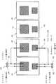
本発明の実施の形態1にかかる半導体ウエハの検査装置について、図1を参照して説明する。図1は、本実施の形態にかかる半導体ウエハの検査装置の構成を示す模式的概略図である。ここでは説明の簡略化のため、パワーMOSFET100が、第1のチップ、第2のチップ、第3のチップ、第4のチップと、4個並列に形成されている半導体ウエハを検査する場合について図示している。各パワーMOSEFT100の表面にはソースアルミパッド101及びゲートアルミパッド102が形成されており、一方、裏面には全てのチップに共通の裏面ドレイン端子(不図示)が略全面に形成されている。
A semiconductor wafer inspection apparatus according to a first embodiment of the present invention will be described with reference to FIG. FIG. 1 is a schematic diagram showing a configuration of a semiconductor wafer inspection apparatus according to the present embodiment. Here, for simplification of description, a case where the
これらのパワーMOSFET100の性能検査を行うウエハ検査装置200は、ソース電圧端子Sv201、ソース電流端子Si202、ゲート電圧端子Gv203、ゲート電流端子Gi204を備えている。また、それぞれの端子は、パワーMOSFET100のソースアルミパッド101及びゲートアルミパッド102に電流や電圧を印加するプローブ205を備えている。また、パワーMOSFET100の裏面ドレイン端子に接触されるテスターのドレイン端子(不図示)を備えている。 A
ソース電流端子Si202は、隣接する2つのパワーMOSFET100のソースアルミパッド101に同時に接触するように、ソース電流端子Si202と電気的に接続された2つのプローブ205を備えている。 The source current terminal Si202 includes two
また、ゲート電流端子Gi204は、隣接する2つのパワーMOSFET100のゲートアルミパッド102に同時に接触するように、ゲート電流端子Gi204と電気的に接続された2つのプローブ205を備えている。 In addition, the gate current terminal Gi204 includes two
半導体ウエハ上のパワーMOSFET100の性能検査を行う場合、まず、第1のチップのソースアルミパッド101には、ソース電圧端子Svに接続されたプローブ205と、ソース電流端子Siに接続されたプローブ205の2本が接触される。また、第2のチップのゲートアルミパッド102には、ゲート電圧端子Gvに接続されたプローブ205と、ゲート電流端子Giに接続されたプローブ205の2本が接触される。 When performing the performance inspection of the
同時に、第1のチップに隣接した第2のチップのソースアルミパッド101上には、ソース電流端子Si202と電気的に接続されているプローブ205が接触される。また、第2のチップのゲートアルミパッド102上には、ゲート電流端子Gi204と電気的に接続されているプローブ205が接触される。 At the same time, the
すなわち、ソース電流端子Si202に接続されている2本のプローブ205はそれぞれ、隣接する2つのパワーMOSFET100のソースアルミパッド101に同時に接触される。また、ゲート電流端子Gi204に接続されている2本のプローブはそれぞれ、隣接する2つのパワーMOSFET100のゲートアルミパッド102に同時に接触される。 That is, the two
ソース電圧端子Sv201から第1のチップのソースアルミパッド101に印加される所定の電圧は、ソース電流端子Siに接続されたプローブ205を介して、第2のチップのソースアルミパッド101にも印加される。また、ゲート電圧端子Gv203から第1のチップのゲートアルミパッド102に印加される所定の電圧は、ゲート電流端子Giに接続されたプローブ205を介して、第2のチップのゲートアルミパッド102にも印加される。つまり、隣接する2つのパワーMOSFET100の性能検査を同時に行うことが可能である。 A predetermined voltage applied from the source voltage terminal Sv201 to the
なお、ソース電圧端子Sv201及びゲート電圧端子Gv203にそれぞれ2本のプローブ205を接続し、隣接する2つのパワーMOSFET100のソースアルミパッド101及びゲートアルミパッド102にそれぞれ電圧を印加するようにしてもよい。 Note that two
図2を参照して、半導体ウエハの検査方法について説明する。図2(a)は、ウエハ検査装置200に接続された状態の第1のチップ及び第2のチップの回路図であり、図2(b)は、ウエハ検査装置200によって測定された電気的特性を示す図である。ウエハ検査装置200の各プローブ205は、上述したように、第1のチップ及び第2のチップのソースアルミパッド101及びゲートアルミパッド102にそれぞれ接続されている。 A semiconductor wafer inspection method will be described with reference to FIG. 2A is a circuit diagram of the first chip and the second chip that are connected to the
図2(a)に示すように、2つのパワーMOSFET100は、並列に接続されている。このような接続状態において、まず、ある特定のゲート電圧を印加する。このゲート電圧は、任意の値とする。そして、第1のチップ及び第2のチップをまとめたドレイン電流I−ドレイン電圧Vの特性を一度に測定する。その後、あらかじめ設定されたあるドレイン電圧時のドレイン電流が判定規格内(図2(b)斜線部)であれば、第1のチップ及び第2のチップのドレイン電流I−ドレイン電圧V特性は合格と判定する。すなわち、第1のチップ及び第2のチップはまとめて良品と判定される。 As shown in FIG. 2A, the two
一方、あらかじめ設定されたあるドレイン電圧時のドレイン電流が判定規格外(図2(b)白い部分)であれば、第1のチップ及び第2のチップのドレイン電流I−ドレイン電圧V特性は不合格と判定する。すなわち、第1のチップ及び第2のチップはまとめて不良品と判定される。つまり、2つのチップのうち一方でも不良品である場合、これら2つともが不良品であるとする。 On the other hand, if the drain current at a certain drain voltage set in advance is out of the determination standard (white portion in FIG. 2B), the drain current I-drain voltage V characteristics of the first chip and the second chip are not good. Judged as passing. That is, the first chip and the second chip are collectively determined to be defective. That is, when one of the two chips is a defective product, it is assumed that both of these chips are defective products.
その後、第3のチップ及び第4のチップを同時に性能検査のための測定を行う。第3のチップ及び第4のチップを測定するときも同様に、2チップ同時に測定し、パワーMOSFET100の良否判定を実行する。このように図2に示すような電気的に接続した回路において、2つのチップのドレイン電流I−ドレイン電圧Vを1度に測定するため、2つのパワーMOSFET100の良否判定を同時に行うことが可能である。 Thereafter, the third chip and the fourth chip are simultaneously measured for performance inspection. Similarly, when measuring the third chip and the fourth chip, the two chips are also measured at the same time, and the pass / fail judgment of the
パワーMOSFETは、比較的チップ自体のコストは低く、良品率が高い。したがって、製造コストの上昇は、チップの性能検査にかかる時間が支配的な要因となっていた。しかし、上述のように、2つまとめて良否判定を行っているので、検査にかかる時間を短縮することが可能である。 The power MOSFET has a relatively low cost of the chip itself and a high yield rate. Therefore, the increase in manufacturing cost has become a dominant factor for the time required for chip performance inspection. However, as described above, since the pass / fail determination is performed for two, it is possible to reduce the time required for the inspection.
また、隣接する2つのパワーMOSFET100が、1つのパッケージとして同時にマウントされる場合、従来、1つ1つ測定を行っていた場合には、片方のみが良品と判定されても、パッケージとしては不良品となっていた。しかし、同時にマウントする2つのパワーMOSFET100をまとめて良否判定しているため、ムダな検査(片方のみが良品と判定される検査)を省略することができる。 In addition, when two
このように、2つのパワーMOSFET100を1つのセットとする製品(1パッケージ)を製造する場合の半導体ウエハの検査において、測定時間を1/2に短縮することができる。したがって、半導体ウエハの検査工程にかかる時間を短縮することができ、単位時間当たりの生産数を向上させ、製造コストを低減させることが可能である。 Thus, in the inspection of a semiconductor wafer when manufacturing a product (one package) having two
実施の形態2.
次に、本発明の実施の形態2にかかる半導体ウエハの検査装置200の構成について説明する。図3は、実施の形態2にかかる半導体ウエハの検査装置200の構成を説明する模式的概略図である。図3において、図1と同じ構成要素には同じ符号を付し、説明を省略する。本実施の形態において、実施の形態1と異なる点は、ソース電流端子Si202、ゲート電流端子Gi204にそれぞれ接続されているプローブ205が3つずつ設けられている点である。
Next, the configuration of the semiconductor
ここでもまた、上述したように、説明の簡略化のため、パワーMOSFET100が、第1のチップ、第2のチップ、第3のチップ、第4のチップと、4個並列に形成されている半導体ウエハを検査する場合について図示している。各パワーMOSEFT100の表面にはソースアルミパッド101及びゲートアルミパッド102が形成されており、一方、裏面には全てのチップに共通の裏面ドレイン端子(不図示)が略全面に形成されている。 Again, as described above, for simplicity of explanation, the
これらのパワーMOSFET100の性能検査を行うウエハ検査装置200は、実施の形態1において説明したように、ソース電圧端子Sv201、ソース電流端子Si202、ゲート電圧端子Gv203、ゲート電流端子Gi204を備えている。また、それぞれの端子は、MOSFET100のソースアルミパッド101及びゲートアルミパッド102に電流や電圧を印加するプローブ205を備えている。また、MOSFET100の裏面ドレイン端子に接触されるテスターのドレイン端子(不図示)を備えている。 As described in the first embodiment, the
ソース電流端子Si202は、隣接する3つのMOSFET100のソースアルミパッド101に同時に接触するように、電気的に接続された3つのプローブ205をそれぞれ備えている。また、ゲート電流端子Gi204は、隣接する3つのMOSFET100のゲートアルミパッド102に同時に接触するように、ゲート電流端子Gi204と電気的に接続された3つのプローブ205をそれぞれ有している。 The source current terminal Si202 includes three
半導体ウエハ上のMOSFET100の性能検査を行う場合、まず、上述したように、第1のチップのソースアルミパッド101には、ソース電圧端子Svに接続されたプローブ205と、ソース電流端子Siに接続されたプローブ205の2本が接触される。また、第2のチップのゲートアルミパッド102には、ゲート電圧端子Gvに接続されたプローブ205と、ゲート電流端子Giに接続されたプローブ205の2本が接触される。 When performing the performance test of the
同時に、第1のチップに隣接した第2のチップのソースアルミパッド101上には、ソース電流端子Si202と電気的に接続されているプローブ205が接触される。また、第2のチップのゲートアルミパッド102上には、ゲート電流端子Gi204と電気的に接続されているプローブ205が接触される。さらに、第2のチップに隣接した第3のチップのソースアルミパッド101上には、ソース電流端子Si202と電気的に接続されているもう1つのプローブ205が接触されている。また、第3のチップのゲートアルミパッド102上には、ゲート電流端子Gi204と電気的に接続されているもう1つのプローブ205が接触される。 At the same time, the
すなわち、ソース電流端子Si202に接続されている3本のプローブ205は、隣接する3つのパワーMOSFET100のソースアルミパッド101に同時に接触する。また、ゲート電流端子Gi203に接続されている3本のプローブは、隣接する3つのパワーMOSFET100のゲートアルミパッド102に同時に接触する。つまり、3つのパワーMOSFET100の性能検査を同時に行うことが可能である。 That is, the three
ソース電圧端子Sv201から第1のチップのソースアルミパッド101に印加される所定の電圧は、ソース電流端子Siに接続された3本のプローブ205を介して、第2のチップ及び第3のチップのソースアルミパッド101にも印加される。また、ゲート電圧端子Gv203から第1のチップのゲートアルミパッド102に印加される所定の電圧は、ゲート電流端子Giに接続されたプローブ205を介して、第2のチップ及び第3のチップのゲートアルミパッド102にも印加される。つまり、隣接する3つのパワーMOSFET100の性能検査を同時に行うことが可能である。 A predetermined voltage applied from the source voltage terminal Sv201 to the
なお、ソース電圧端子Sv201及びゲート電圧端子Gv203にそれぞれ3本のプローブ205を接続し、隣接する3つのパワーMOSFET100のソースアルミパッド101及びゲートアルミパッド102にそれぞれ電圧を印加するようにしてもよい。 Note that three
これらのパワーMOSFET100の良否判定は、上述したような検査方法を用いて実行する。すなわち、3つのパワーMOSFET100にそれぞれのプローブ205が接続した状態において、まず、ある特定のゲート電圧を印加する。そして、第1のチップ、第2のチップ及び第3のチップをまとめたドレイン電流I−ドレイン電圧Vの特性を一度に測定する。その後、あらかじめ設定されたあるドレイン電圧時のドレイン電流が判定規格内であれば、第1のチップ、第2のチップ及び第3のチップをまとめて良品と判定する。 The quality determination of these
一方、あらかじめ設定されたあるドレイン電圧時のドレイン電流が判定規格外であれば、第1のチップ、第2のチップ及び第3のチップはまとめて不良品と判定される。つまり、3つのチップのうち1つでも不良品である場合、これら3つともが不良品であるとする。 On the other hand, if the drain current at a certain preset drain voltage is outside the determination standard, the first chip, the second chip, and the third chip are collectively determined to be defective. That is, if any one of the three chips is defective, it is assumed that all three chips are defective.
上述のように、3つまとめて良否判定を行っているので、検査にかかる時間をさらに短縮することが可能である。また、隣接する3つのパワーMOSFET100が、1つのパッケージとして同時にマウントされる場合、従来、1つ1つ測定を行っていた場合には、3つのうちの1つのみが良品と判定されても、パッケージとしては不良品となっていた。しかし、同時にマウントする3つのパワーMOSFET100をまとめて良否判定しているため、ムダな検査(3つのチップセットのうちのいずれかが良品と判定されるような検査)を省略することができる。このようにすることによって、3つのチップを1つのセットとする製品(1パッケージ)を製造する工程の半導体ウエハの検査において、測定時間を1/3に短縮することができる。 As described above, since the pass / fail determination is performed for all three, it is possible to further reduce the time required for the inspection. In addition, when three
同様の技術的思想により、N個のチップをひとつのセットとする製品(1パッケージ)を製造する場合、の半導体ウエハの検査において、測定時間を1/Nに短縮することができる。したがって、複数のパワーMOSFET100を1つのセットとして1つのパッケージを製造するときにかかる時間を短縮することができ、単位時間当たりの製造生産数を向上させ、製造コストを低減させることが可能である。 With the same technical idea, when manufacturing a product (one package) having N chips as one set, the measurement time can be shortened to 1 / N in the inspection of the semiconductor wafer. Therefore, it is possible to shorten the time required to manufacture one package with a plurality of
また、ここでは、説明のためにパワーMOSFETを検査する場合について説明したが、これに限定されるものではない。例えば、ダイオードなどを複数個まとめて1つのパッケージとしてマウントする場合などの、半導体ウエハの検査にも用いることができる。 Further, here, the case where the power MOSFET is inspected is described for the sake of explanation, but the present invention is not limited to this. For example, it can be used for inspection of a semiconductor wafer when a plurality of diodes are mounted as a single package.
100 パワーMOSEFT
101 ゲートアルミパッド
102 ソースアルミパッド
200 検査装置
201 ソース電圧端子
202 ソース電流端子
203 ゲート電圧端子
204 ゲート電流端子
205 プローブ100 Power MOSEFT
101
Claims (7)
Translated fromJapanese前記複数の半導体素子に対して同時にゲート電圧を印加するゲート電圧端子と、
前記複数の半導体素子のドレイン−ソース間電流を同時に測定する電流端子とを有し、
ソース電流端子に接続される複数の第1のプローブと、
ゲート電流端子に接続される複数の第2のプローブと、
を有し、
前記複数の第1のプローブを、前記ウエハ上において隣接する半導体素子のソースパッドに同時に接触させ、
前記複数の第2のプローブを、前記ウエハ上において隣接する半導体素子のゲートパッドに同時に接触させ、
ソース電圧端子に接続される第3のプローブと、ゲート電圧端子に接続される第4のプローブとをさらに備え、
前記第3のプローブを前記複数の第1のプローブが接触している前記複数の半導体素子のうちの第1の半導体素子のソースパッドに接触させ、
前記第4のプローブを前記複数の第2のプローブが接触している前記複数の半導体素子のうちの前記第1の半導体素子のゲートパッドに接触させる
ウエハ検査装置。A wafer inspection apparatus in which a plurality of semiconductor elements mounted in one package are formed adjacent to each other,
A gate voltage terminal for simultaneously applying a gate voltage to the plurality of semiconductor elements;
The drain of the plurality of semiconductor devices -have a current terminal to measure the source current at the sametime,
A plurality of first probes connected to a source current terminal;
A plurality of second probes connected to the gate current terminal;
Have
Contacting the plurality of first probes simultaneously with the source pads of adjacent semiconductor elements on the wafer;
Contacting the plurality of second probes simultaneously with the gate pads of adjacent semiconductor elements on the wafer;
A third probe connected to the source voltage terminal; and a fourth probe connected to the gate voltage terminal;
Contacting the third probe with a source pad of a first semiconductor element of the plurality of semiconductor elements in contact with the plurality of first probes;
The wafer inspection apparatus,wherein the fourth probe is brought into contact with a gate pad of the first semiconductor element among the plurality of semiconductor elements in contact with the plurality of second probes .
請求項1に記載のウエハ検査装置。The first probe and the second probe are provided corresponding to the number of adjacent semiconductor elements on the wafer to be mounted on one package.
The wafer inspection apparatus according toclaim 1 .
請求項1または請求項2に記載のウエハ検査装置。The semiconductor elements mounted on the one package and adjacent on the wafer are inspected as one set, and when it is determined as defective, the set is collectively determined as defective.
The wafer inspection apparatus according toclaim 1 or 2 .
請求項1〜請求項3のいずれか1項に記載のウエハ検査装置。The wafer inspection apparatus according to claim 1.
前記複数の半導体素子に対して同時にゲート電圧を印加し、
前記複数の半導体素子のドレイン−ソース間電流を同時に測定し、
ソース電流端子に接続される複数の第1のプローブを前記ウエハ上において隣接する半導体素子のソースパッドに同時に接触させ、
ゲート電流端子に接続される複数の第2のプローブを前記ウエハ上において隣接する半導体素子のゲートパッドに同時に接触させ、
ソース電圧端子に接続される第3のプローブを前記複数の第1のプローブが接触しているソースパッドのうちの1つに接触させ、
ゲート電圧端子に接続される第4のプローブを前記複数の第2のプローブが接触しているゲートパッドのうちの1つに接触させ、
前記1つのパッケージにマウントする隣接する半導体素子を1つのセットとして検査を行い、不良と判定された場合、該セットをまとめて不良と判定する
ウエハの検査方法。A method for inspecting a wafer in which a plurality of semiconductor elements mounted in one package are formed adjacent to each other,
Applying a gate voltage simultaneously to the plurality of semiconductor elements;
Simultaneously measuring drain-source currents of the plurality of semiconductor elements;
A plurality of first probes connected to source current terminals are simultaneously brought into contact with source pads of adjacent semiconductor elements on the wafer;
A plurality of second probes connected to a gate current terminal are simultaneously brought into contact with gate pads of adjacent semiconductor elements on the wafer;
Bringing a third probe connected to a source voltage terminal into contact with one of the source pads in contact with the plurality of first probes;
A fourth probe connected to a gate voltage terminal is brought into contact with one of the gate pads in contact with the plurality of second probes;
An inspection method for a wafer,in which adjacent semiconductor elements mounted on one package are inspected as one set, and when it is determined as defective, the set is collectively determined as defective .
請求項5に記載のウエハ検査方法。The first probe and the second probe are provided corresponding to the number of adjacent semiconductor elements on the wafer to be mounted on one package.
The wafer inspection method according toclaim 5 .
請求項5または請求項6に記載のウエハ検査方法。The wafer inspection method according to claim 5 or 6.
Priority Applications (1)
| Application Number | Priority Date | Filing Date | Title |
|---|---|---|---|
| JP2005004346AJP4744884B2 (en) | 2005-01-11 | 2005-01-11 | Wafer inspection apparatus and wafer inspection method |
Applications Claiming Priority (1)
| Application Number | Priority Date | Filing Date | Title |
|---|---|---|---|
| JP2005004346AJP4744884B2 (en) | 2005-01-11 | 2005-01-11 | Wafer inspection apparatus and wafer inspection method |
Publications (2)
| Publication Number | Publication Date |
|---|---|
| JP2006196546A JP2006196546A (en) | 2006-07-27 |
| JP4744884B2true JP4744884B2 (en) | 2011-08-10 |
Family
ID=36802400
Family Applications (1)
| Application Number | Title | Priority Date | Filing Date |
|---|---|---|---|
| JP2005004346AExpired - Fee RelatedJP4744884B2 (en) | 2005-01-11 | 2005-01-11 | Wafer inspection apparatus and wafer inspection method |
Country Status (1)
| Country | Link |
|---|---|
| JP (1) | JP4744884B2 (en) |
Families Citing this family (1)
| Publication number | Priority date | Publication date | Assignee | Title |
|---|---|---|---|---|
| CN102157415B (en)* | 2011-03-15 | 2015-05-20 | 上海华虹宏力半导体制造有限公司 | Method for testing wafer parameters of bare chips |
Family Cites Families (5)
| Publication number | Priority date | Publication date | Assignee | Title |
|---|---|---|---|---|
| JPS6118144A (en)* | 1984-07-04 | 1986-01-27 | Mitsubishi Electric Corp | Semiconductor device measuring apparatus |
| JP3436183B2 (en)* | 1999-04-28 | 2003-08-11 | 松下電器産業株式会社 | Semiconductor inspection apparatus and inspection method using the same |
| JP2003031627A (en)* | 2001-07-18 | 2003-01-31 | Nippon Inter Electronics Corp | Method of measuring semiconductor chip |
| JP2003121500A (en)* | 2001-10-10 | 2003-04-23 | Mitsubishi Electric Corp | Test apparatus and test method for semiconductor device |
| JP4557507B2 (en)* | 2002-06-13 | 2010-10-06 | パナソニック株式会社 | Semiconductor device and manufacturing method thereof |
- 2005
- 2005-01-11JPJP2005004346Apatent/JP4744884B2/ennot_activeExpired - Fee Related
Also Published As
| Publication number | Publication date |
|---|---|
| JP2006196546A (en) | 2006-07-27 |
Similar Documents
| Publication | Publication Date | Title |
|---|---|---|
| KR100466984B1 (en) | Integrated circuit chip having test element group circuit and method of test the same | |
| CN108267682A (en) | A kind of high-density test chip and its test system and its test method | |
| JP2020150116A (en) | Semiconductor devices and their manufacturing methods | |
| US20120268147A1 (en) | Structure for measuring bump resistance and package substrate comprising the same | |
| JP2008277417A (en) | Semiconductor device and testing method of the same | |
| US7105856B1 (en) | Test key having a chain circuit and a kelvin structure | |
| US20140354325A1 (en) | Semiconductor layout structure and testing method thereof | |
| JP2000503124A (en) | Method for testing integrated circuits | |
| CN103837809B (en) | The IC layout of test MOSFET matching and method of testing | |
| JP4744884B2 (en) | Wafer inspection apparatus and wafer inspection method | |
| CN102128991B (en) | Aging test device and test method thereof | |
| CN100533163C (en) | Wafer capable of implementing aging and electrical test and implementing method thereof | |
| CN115598493A (en) | Detection system, signal source and power supply device of integrated circuit device | |
| JP5358125B2 (en) | Semiconductor device and semiconductor chip crack detection method | |
| JP2006310495A (en) | Semiconductor integrated circuit wafer, test method thereof, and manufacturing method of semiconductor integrated circuit component | |
| JP2019100951A (en) | Inspection method of semiconductor device, and inspection apparatus | |
| CN103688180B (en) | The verifying attachment of semiconductor device, checking system, the method for inspection and the production method of semiconductor device inspected | |
| CN104459272A (en) | Apparatus of measuring semiconductor device | |
| JP2013234920A (en) | Semiconductor integrated circuit device manufacturing method and program | |
| US8896339B2 (en) | Method for testing semiconductor wafer | |
| US20030210068A1 (en) | Apparatus of testing semiconductor | |
| JP2008186829A (en) | Tool for inspecting wafer, and measurement method using the same | |
| JP2005077339A (en) | Composite semiconductor device and test method thereof | |
| KR100934793B1 (en) | Semiconductor device test method and apparatus and proper stress voltage detection method | |
| JP2018136197A (en) | Detector detecting physical quantity of fluid |
Legal Events
| Date | Code | Title | Description |
|---|---|---|---|
| A621 | Written request for application examination | Free format text:JAPANESE INTERMEDIATE CODE: A621 Effective date:20071015 | |
| A977 | Report on retrieval | Free format text:JAPANESE INTERMEDIATE CODE: A971007 Effective date:20080327 | |
| A131 | Notification of reasons for refusal | Free format text:JAPANESE INTERMEDIATE CODE: A131 Effective date:20100907 | |
| A521 | Written amendment | Free format text:JAPANESE INTERMEDIATE CODE: A523 Effective date:20101108 | |
| TRDD | Decision of grant or rejection written | ||
| A01 | Written decision to grant a patent or to grant a registration (utility model) | Free format text:JAPANESE INTERMEDIATE CODE: A01 Effective date:20110506 | |
| A01 | Written decision to grant a patent or to grant a registration (utility model) | Free format text:JAPANESE INTERMEDIATE CODE: A01 | |
| A61 | First payment of annual fees (during grant procedure) | Free format text:JAPANESE INTERMEDIATE CODE: A61 Effective date:20110511 | |
| FPAY | Renewal fee payment (event date is renewal date of database) | Free format text:PAYMENT UNTIL: 20140520 Year of fee payment:3 | |
| R150 | Certificate of patent or registration of utility model | Free format text:JAPANESE INTERMEDIATE CODE: R150 | |
| S531 | Written request for registration of change of domicile | Free format text:JAPANESE INTERMEDIATE CODE: R313531 | |
| R350 | Written notification of registration of transfer | Free format text:JAPANESE INTERMEDIATE CODE: R350 | |
| LAPS | Cancellation because of no payment of annual fees |