JP4744788B2 - Manufacturing method of semiconductor device - Google Patents
Manufacturing method of semiconductor deviceDownload PDFInfo
- Publication number
- JP4744788B2 JP4744788B2JP2003144670AJP2003144670AJP4744788B2JP 4744788 B2JP4744788 B2JP 4744788B2JP 2003144670 AJP2003144670 AJP 2003144670AJP 2003144670 AJP2003144670 AJP 2003144670AJP 4744788 B2JP4744788 B2JP 4744788B2
- Authority
- JP
- Japan
- Prior art keywords
- insulating film
- contact plug
- contact
- film
- conductive
- Prior art date
- Legal status (The legal status is an assumption and is not a legal conclusion. Google has not performed a legal analysis and makes no representation as to the accuracy of the status listed.)
- Expired - Fee Related
Links
Images


Classifications
- H—ELECTRICITY
- H10—SEMICONDUCTOR DEVICES; ELECTRIC SOLID-STATE DEVICES NOT OTHERWISE PROVIDED FOR
- H10D—INORGANIC ELECTRIC SEMICONDUCTOR DEVICES
- H10D84/00—Integrated devices formed in or on semiconductor substrates that comprise only semiconducting layers, e.g. on Si wafers or on GaAs-on-Si wafers
- H—ELECTRICITY
- H10—SEMICONDUCTOR DEVICES; ELECTRIC SOLID-STATE DEVICES NOT OTHERWISE PROVIDED FOR
- H10D—INORGANIC ELECTRIC SEMICONDUCTOR DEVICES
- H10D1/00—Resistors, capacitors or inductors
- H10D1/60—Capacitors
- H10D1/68—Capacitors having no potential barriers
- H10D1/692—Electrodes
- H10D1/694—Electrodes comprising noble metals or noble metal oxides
- H—ELECTRICITY
- H01—ELECTRIC ELEMENTS
- H01L—SEMICONDUCTOR DEVICES NOT COVERED BY CLASS H10
- H01L21/00—Processes or apparatus adapted for the manufacture or treatment of semiconductor or solid state devices or of parts thereof
- H01L21/70—Manufacture or treatment of devices consisting of a plurality of solid state components formed in or on a common substrate or of parts thereof; Manufacture of integrated circuit devices or of parts thereof
- H01L21/71—Manufacture of specific parts of devices defined in group H01L21/70
- H01L21/768—Applying interconnections to be used for carrying current between separate components within a device comprising conductors and dielectrics
- H01L21/76838—Applying interconnections to be used for carrying current between separate components within a device comprising conductors and dielectrics characterised by the formation and the after-treatment of the conductors
- H01L21/76841—Barrier, adhesion or liner layers
- H01L21/7687—Thin films associated with contacts of capacitors
- H—ELECTRICITY
- H01—ELECTRIC ELEMENTS
- H01L—SEMICONDUCTOR DEVICES NOT COVERED BY CLASS H10
- H01L21/00—Processes or apparatus adapted for the manufacture or treatment of semiconductor or solid state devices or of parts thereof
- H01L21/70—Manufacture or treatment of devices consisting of a plurality of solid state components formed in or on a common substrate or of parts thereof; Manufacture of integrated circuit devices or of parts thereof
- H01L21/71—Manufacture of specific parts of devices defined in group H01L21/70
- H01L21/768—Applying interconnections to be used for carrying current between separate components within a device comprising conductors and dielectrics
- H01L21/76838—Applying interconnections to be used for carrying current between separate components within a device comprising conductors and dielectrics characterised by the formation and the after-treatment of the conductors
- H01L21/76877—Filling of holes, grooves or trenches, e.g. vias, with conductive material
- H—ELECTRICITY
- H10—SEMICONDUCTOR DEVICES; ELECTRIC SOLID-STATE DEVICES NOT OTHERWISE PROVIDED FOR
- H10B—ELECTRONIC MEMORY DEVICES
- H10B12/00—Dynamic random access memory [DRAM] devices
- H10B12/01—Manufacture or treatment
- H10B12/02—Manufacture or treatment for one transistor one-capacitor [1T-1C] memory cells
- H10B12/03—Making the capacitor or connections thereto
- H10B12/033—Making the capacitor or connections thereto the capacitor extending over the transistor
- H—ELECTRICITY
- H10—SEMICONDUCTOR DEVICES; ELECTRIC SOLID-STATE DEVICES NOT OTHERWISE PROVIDED FOR
- H10B—ELECTRONIC MEMORY DEVICES
- H10B12/00—Dynamic random access memory [DRAM] devices
- H10B12/01—Manufacture or treatment
- H10B12/09—Manufacture or treatment with simultaneous manufacture of the peripheral circuit region and memory cells
- H—ELECTRICITY
- H10—SEMICONDUCTOR DEVICES; ELECTRIC SOLID-STATE DEVICES NOT OTHERWISE PROVIDED FOR
- H10B—ELECTRONIC MEMORY DEVICES
- H10B12/00—Dynamic random access memory [DRAM] devices
- H10B12/30—DRAM devices comprising one-transistor - one-capacitor [1T-1C] memory cells
- H10B12/48—Data lines or contacts therefor
- H10B12/485—Bit line contacts
- H—ELECTRICITY
- H10—SEMICONDUCTOR DEVICES; ELECTRIC SOLID-STATE DEVICES NOT OTHERWISE PROVIDED FOR
- H10B—ELECTRONIC MEMORY DEVICES
- H10B12/00—Dynamic random access memory [DRAM] devices
- H10B12/50—Peripheral circuit region structures
- H—ELECTRICITY
- H10—SEMICONDUCTOR DEVICES; ELECTRIC SOLID-STATE DEVICES NOT OTHERWISE PROVIDED FOR
- H10D—INORGANIC ELECTRIC SEMICONDUCTOR DEVICES
- H10D1/00—Resistors, capacitors or inductors
- H10D1/01—Manufacture or treatment
- H10D1/041—Manufacture or treatment of capacitors having no potential barriers
- H10D1/042—Manufacture or treatment of capacitors having no potential barriers using deposition processes to form electrode extensions
- H—ELECTRICITY
- H10—SEMICONDUCTOR DEVICES; ELECTRIC SOLID-STATE DEVICES NOT OTHERWISE PROVIDED FOR
- H10D—INORGANIC ELECTRIC SEMICONDUCTOR DEVICES
- H10D1/00—Resistors, capacitors or inductors
- H10D1/60—Capacitors
- H10D1/68—Capacitors having no potential barriers
- H10D1/692—Electrodes
- H10D1/711—Electrodes having non-planar surfaces, e.g. formed by texturisation
- H10D1/716—Electrodes having non-planar surfaces, e.g. formed by texturisation having vertical extensions
- H—ELECTRICITY
- H10—SEMICONDUCTOR DEVICES; ELECTRIC SOLID-STATE DEVICES NOT OTHERWISE PROVIDED FOR
- H10B—ELECTRONIC MEMORY DEVICES
- H10B12/00—Dynamic random access memory [DRAM] devices
- H10B12/30—DRAM devices comprising one-transistor - one-capacitor [1T-1C] memory cells
- H10B12/31—DRAM devices comprising one-transistor - one-capacitor [1T-1C] memory cells having a storage electrode stacked over the transistor
- H10B12/312—DRAM devices comprising one-transistor - one-capacitor [1T-1C] memory cells having a storage electrode stacked over the transistor with a bit line higher than the capacitor
- H—ELECTRICITY
- H10—SEMICONDUCTOR DEVICES; ELECTRIC SOLID-STATE DEVICES NOT OTHERWISE PROVIDED FOR
- H10B—ELECTRONIC MEMORY DEVICES
- H10B12/00—Dynamic random access memory [DRAM] devices
- H10B12/30—DRAM devices comprising one-transistor - one-capacitor [1T-1C] memory cells
- H10B12/48—Data lines or contacts therefor
- H10B12/482—Bit lines
Landscapes
- Engineering & Computer Science (AREA)
- Manufacturing & Machinery (AREA)
- Power Engineering (AREA)
- Physics & Mathematics (AREA)
- Condensed Matter Physics & Semiconductors (AREA)
- General Physics & Mathematics (AREA)
- Computer Hardware Design (AREA)
- Microelectronics & Electronic Packaging (AREA)
- Semiconductor Memories (AREA)
- Internal Circuitry In Semiconductor Integrated Circuit Devices (AREA)
Description
Translated fromJapanese【0001】
【発明の属する技術分野】
この発明は、半導体基板上にメモリデバイスとロジックデバイスとが形成された、メモリ・ロジック混載型の半導体装置の製造方法に関する。
【0002】
【従来の技術】
近年、メモリ・ロジック混載型の半導体装置の微細化にともなって、メモリセルの面積が縮小されている。そして、メモリセルの面積が縮小した場合であっても一定のキャパシタ容量を確保するために、メモリセルのキャパシタにMIM(Metal−Insulator−Metal)キャパシタを採用するようになっている。
【0003】
メモリセルのキャパシタにMIMキャパシタを採用した場合、その誘電体膜を形成するプロセスにおいて、下部電極と接続されるコンタクトプラグや、その周辺のコンタクトプラグが酸化されて高抵抗化し、コンタクト抵抗が増加する問題が生じることがあった。この問題を解決するために、コンタクトプラグの上端部に酸化防止用のバリア層を設けて、コンタクト抵抗の増加を防止する技術が特許文献1に開示されている。なお、キャパシタを備える半導体装置に関する技術が特許文献2,3にも開示されている。
【0004】
【特許文献1】
特開2001−267516号公報
【特許文献2】
特開2001−284541号公報
【非特許文献1】
特開平10−150161号公報
【0005】
【発明が解決しようとする課題】
しかしながら、メモリ・ロジック混載型の半導体装置においては、メモリデバイスでのコンタクト抵抗の低減と、ロジックデバイスでのコンタクト抵抗の低減とを両立させることが困難であった。
【0006】
そこで、本発明は上述の問題に鑑みて成されたものであり、MIMキャパシタの誘電体膜の形成時に酸化処理が実行される場合であっても、メモリデバイスでのコンタクト抵抗の低減とロジックデバイスでのコンタクト抵抗の低減とを両立させることが可能な技術を提供することを目的とする。
【0007】
【課題を解決するための手段】
この発明の半導体装置の製造方法は、(a)メモリデバイスが形成されるメモリ領域と、ロジックデバイスが形成されるロジック領域とを有する半導体基板上に第1の絶縁膜を形成する工程と、(b)前記メモリ領域における前記半導体基板と電気的に接続され、上面が前記第1の絶縁膜から露出する第1のコンタクトプラグと、前記ロジック領域における前記半導体基板と電気的に接続され、上面が前記第1の絶縁膜から露出する第2のコンタクトプラグとを、前記第1の絶縁膜内に形成する工程とを備え、前記工程(b)で形成される前記第1のコンタクトプラグは、第1の導電性膜と、前記第1の導電性膜の上面を覆うように前記第1の導電性膜上に形成された、前記第1の導電性膜の酸化を防止するための第1の導電性バリア層を有し、(c)前記第1の導電性バリア層と接触するMIM(Metal−Insulator−Metal)キャパシタを形成するとともに、前記工程(b)の実行によって得られた構造の上面上に前記MIMキャパシタを覆う第2の絶縁膜を形成する工程と、(d)前記工程(c)の後に、前記第2のコンタクトプラグと接触する第3のコンタクトプラグを前記第2の絶縁膜内に形成する工程とを更に備え、前記工程(c)で形成される前記MIMキャパシタは、前記第1の導電性バリア層と接触する下部電極と、上部電極と、それらの間に挟まれている誘電体膜とを有し、前記工程(b)において、前記メモリ領域における前記半導体基板と電気的に接続され、上面が前記第1の絶縁膜から露出する第4のコンタクトプラグを前記第1の絶縁膜内に更に形成し、前記工程(d)において、前記第4のコンタクトプラグと接触する第5のコンタクトプラグを前記第2の絶縁膜内に更に形成し、前記工程(b)で形成される前記第4のコンタクトプラグは、第2の導電性膜と、前記第2の導電性膜の上面を覆うように前記第2の導電性膜上に形成された、前記第2の導電性膜の酸化を防止するための第2の導電性バリア層を有し、前記第2の導電性膜は前記第2の導電性バリア層よりも導電率が高く、前記工程(d)は、(d−1)前記第2の導電性バリア層に達する第1のコンタクトホールを前記第2の絶縁膜に形成する工程と、(d−2)前記工程(d−1)の実行によって露出した前記第2の導電性バリア層を除去して前記第2の導電性膜を露出し、前記第1の絶縁膜に凹部を形成する工程と、(d−3)前記第1のコンタクトホールとそれに連通する前記凹部とを充填する前記第5のコンタクトプラグを形成する工程とを含む。
【0008】
また、この発明の第2の半導体装置の製造方法は、(a)メモリデバイスが形成されるメモリ領域と、ロジックデバイスが形成されるロジック領域とを有する半導体基板上に第1の絶縁膜を形成する工程と、(b)前記メモリ領域における前記半導体基板と電気的に接続され、上面が前記第1の絶縁膜から露出する第1のコンタクトプラグと、前記ロジック領域における前記半導体基板と電気的に接続され、上面が前記第1の絶縁膜から露出する第2のコンタクトプラグとを、前記第1の絶縁膜内に形成する工程とを備え、前記工程(b)で形成される前記第1のコンタクトプラグは、第1の導電性膜と、前記第1の導電性膜の上面を覆うように前記第1の導電性膜上に形成された、前記第1の導電性膜の酸化を防止するための第1の導電性バリア層を有し、(c)前記第1の導電性バリア層と接触するMIM(Metal−Insulator−Metal)キャパシタを形成するとともに、前記工程(b)の実行によって得られた構造の上面上に前記MIMキャパシタを覆う第2の絶縁膜を形成する工程と、(d)前記工程(c)の後に、前記第2のコンタクトプラグと接触する第3のコンタクトプラグを前記第2の絶縁膜内に形成する工程とを更に備え、前記工程(c)で形成される前記MIMキャパシタは、前記第1の導電性バリア層と接触する下部電極と、上部電極と、それらの間に挟まれている誘電体膜とを有し、前記工程(b)で形成される前記第2のコンタクトプラグは、第2の導電性膜と、前記第2の導電性膜の上面を覆うように前記第2の導電性膜上に形成された、前記第2の導電性膜の酸化を防止するための第2の導電性バリア層を有し、前記第2の導電性膜は前記第2の導電性バリア層よりも導電率が高く、前記工程(d)は、(d−1)前記第2の導電性バリア層に達する第1のコンタクトホールを前記第2の絶縁膜に形成する工程と、(d−2)前記工程(d−1)の実行によって露出した前記第2の導電性バリア層を除去して前記第2の導電性膜を露出し、前記第1の絶縁膜に凹部を形成する工程と、(d−3)前記第1のコンタクトホールとそれに連通する前記凹部とを充填する前記第3のコンタクトプラグを形成する工程とを含む。
【0010】
【発明の実施の形態】
実施の形態1.
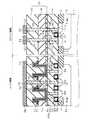
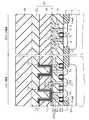
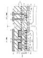
図1〜16は本発明の実施の形態1に係る半導体装置の製造方法を工程順に示す断面図である。本実施の形態1に係る半導体装置は、メモリ・ロジック混載型の半導体装置であって、メモリデバイスとしては例えばCUB(Capacitor Under Bit line)構造のメモリセルを有するDRAMを備え、ロジックデバイスとしては例えばサリサイドCMOSトランジスタを備えている。また、DRAMメモリセルのキャパシタとして例えばConcave型MIMキャパシタを備えている。以下に、図1〜16を参照して本実施の形態1に係る半導体装置の製造方法について説明する。
【0011】
図1に示されるように、まず、周知のLOCOS分離技術やトレンチ分離技術によって、例えばn型のシリコン基板である半導体基板1の上面内に素子分離絶縁膜2を形成する。そして、メモリデバイスが形成される領域(以後、「メモリ領域」と呼ぶ)における半導体基板1の上面内にp型のウェル領域53を形成し、ロジックデバイスが形成される領域(以後、「ロジック領域」と呼ぶ)における半導体基板1の上面内にp型のウェル領域3を形成する。
【0012】
次に、メモリ領域におけるウェル領域53の上面内に、互いに所定距離を成す複数のn型のソース・ドレイン領域59を形成するとともに、それらのソース・ドレイン領域59の間のウェル領域53の上面上にゲート構造61を形成する。また、ロジック領域におけるウェル領域3の上面内に、互いに所定距離を成す複数のn型のソース・ドレイン領域9を形成するとともに、それらのソース・ドレイン領域9の間のウェル領域3の上面上にゲート構造11を形成する。
【0013】
メモリ領域のゲート構造61は、例えばシリコン酸化膜が採用されるゲート絶縁膜55と、例えば多結晶シリコン膜が採用されるゲート電極56と、例えばシリコン窒化膜が採用されるサイドウォール60とを備えている。ゲート構造61の形成後においては、ソース・ドレイン領域59の間のウェル領域53の上面上にゲート絶縁膜55が設けられており、ゲート絶縁膜55上にゲート電極56が設けられている。そして、ゲート絶縁膜55及びゲート電極56の側面上にサイドウォール60が設けられている。
【0014】
ロジック領域のゲート構造11は、例えばシリコン酸化膜が採用されるゲート絶縁膜5と、例えば多結晶シリコン膜が採用されるゲート電極6と、例えばシリコン窒化膜が採用されるサイドウォール10とを備えている。ゲート構造11の形成後においては、ソース・ドレイン領域9の間のウェル領域3の上面上にゲート絶縁膜5が設けられており、ゲート絶縁膜5上にゲート電極6が設けられている。そして、ゲート絶縁膜5及びゲート電極6の側面上にサイドウォール10が設けられている。
【0015】
次に、ゲート電極6,56の上面及びソース・ドレイン領域9,59の上面をシリサイド化して、各ゲート電極6.56の上面上にシリサイド膜12を形成するとともに、各ソース・ドレイン領域9,59の上面上にシリサイド膜12を形成する。なお、シリサイド膜12には例えばコバルトシリサイド膜が採用される。
【0016】
次に図2に示されるように、ゲート構造11,61を覆って半導体基板1上に絶縁膜14を形成する。絶縁膜14は例えばBPTEOS膜が採用され、層間絶縁膜として機能する。
【0017】
次に、所定の開口パターンを有するレジスト(図示せず)を写真製版法によって絶縁膜14上に形成し、かかるレジストをマスクに用いて絶縁膜14をエッチングして部分的に除去する。このときのエッチングでは、C4F6とO2とArとの混合ガスを使用する異方性ドライエッチングが採用される。そして、マスクに使用したレジストを除去する。
【0018】
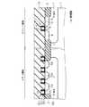
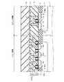
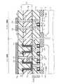
これにより、図3に示されるように、メモリ領域における半導体基板1上のシリサイド膜12に達するコンタクトホール65と、ロジック領域における半導体基板1上のシリサイド膜12に達するコンタクトホール15とが絶縁膜14に形成される。
【0019】
次に、コンタクトホール15,65を充填する、タングステン等から成る高融点金属膜を全面に形成する。そして、例えばCMP法を用いて絶縁膜14の上面上の高融点金属膜を除去する。これにより、図4に示されるように、高融点金属膜から成りコンタクトホール15を充填する導電性膜16と、高融点金属膜から成りコンタクトホール65を充填する導電性膜66とが絶縁膜14内に形成される。
【0020】
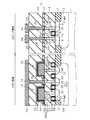
次に図5に示されるように、エキシマ露光対応のレジスト30を全面に形成し、後の工程で形成されるキャパシタと電気的に接続される導電性膜66の上面を露出する開口パターンを、エキシマレーザーを光源として用いた写真製版法によってレジスト30に形成する。そして図6に示されるように、レジスト30をマスクに用いて露出している部分に対してエッチングを実行し、キャパシタと接続される導電性膜66の上端部を選択的に除去する。これにより、メモリ領域における絶縁膜14に凹部81が形成される。このときのエッチングでは、エッチングガスとしてSF6を使用する異方性ドライエッチングが採用される。
【0021】
次に図7に示されるように、マスクに使用したレジスト30を除去する。そして、窒化チタン(TiN)、窒化タンタル(TaN)、あるいは窒化チタンシリサイド(TiSiN)等から成り、各凹部81を充填するバリア層材料を全面に形成し、例えばCMP法を用いて凹部81よりも上方のバリア層材料を除去する。これにより、図8に示されるように、窒化チタン、窒化タンタル、あるいは窒化チタンシリサイド等から成り、各凹部81を充填する導電性バリア層82が絶縁膜14内に形成される。
【0022】
以上の工程により、メモリ領域における絶縁膜14には、導電性膜66から成るコンタクトプラグ83aと、上端部に導電性バリア層82を、それ以外の部分に導電性膜66を有するコンタクトプラグ83bとが形成される。また、ロジック領域における絶縁膜14には、導電性膜16から成るコンタクトプラグ33が形成される。なお、使用されている材料から明らかなように、導電性バリア層82は導電性膜16,66よりも導電率が低い。
【0023】
コンタクトプラグ33は、その上面が絶縁膜14から露出しており、半導体基板1の上面内に形成されたソース・ドレイン領域9とシリサイド膜12を介して電気的に接続されている。
【0024】
コンタクトプラグ83aは、その上面が絶縁膜14から露出しており、互いに隣り合うソース・ドレイン領域59のうち、後の工程で形成されるビット線と電気的に接続されるソース・ドレイン領域59とシリサイド膜12を介して電気的に接続されている。
【0025】
コンタクトプラグ83bは、その上面が、つまり導電性バリア層82の上面が絶縁膜14から露出しており、互いに隣り合うソース・ドレイン領域59のうち、後の工程で形成されるキャパシタと電気的に接続されるソース・ドレイン領域59とシリサイド膜12を介して電気的に接続されている。
【0026】
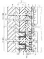
次に図9に示されるように、絶縁膜14及びコンタクトプラグ33,83a,83bの上に、例えばシリコン窒化膜が採用されるストッパ膜17を形成する。そして、ストッパ膜17上に層間絶縁膜18を形成する。層間絶縁膜18には例えばBPTEOS膜が採用される。
【0027】
次に、所定の開口パターンを有するレジスト(図示せず)を層間絶縁膜18上に形成し、かかるレジストをマスクに用いて、ストッパ膜17をエッチングストッパとして、層間絶縁膜18をエッチングして除去する。このときのエッチングでは、C4F6とO2とArとの混合ガスを使用する異方性ドライエッチングが採用される。
【0028】
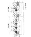
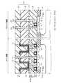
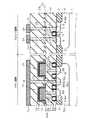
そして、層間絶縁膜18のエッチングの際に使用したレジストを再度マスクに使用して、露出しているストッパ膜17をエッチングして除去し、その後レジストを除去する。このときのエッチングでは、CHF3をエッチングガスとして使用する異方性ドライエッチングが採用される。これにより、図10に示されるように、キャパシタと接続されるコンタクトプラグ83bを露出させる開口部69が層間絶縁膜18内及びストッパ膜17内に形成される。
【0029】
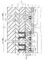
次に、コンタクトプラグ83bの導電性バリア層82に接触する、DRAMメモリセルのキャパシタを開口部69内に形成する。具体的には、まずルテニウム(Ru)、窒化チタン(TiN)、あるいは白金(Pt)等から成る下部電極材料を全面に形成する。そして、開口部69にレジスト(図示せず)を充填し、層間絶縁膜18の上面上の下部電極材料を異方性ドライエッチングにて除去し、その後レジストを除去する。これにより、図11に示されるように、ルテニウム、窒化チタン、あるいは白金等から成るキャパシタの下部電極70が開口部69内に形成される。なお、異方性ドライエッチングで層間絶縁膜18の上面上の下部電極材料を除去したが、CMP法を用いて、かかる電極材料を除去しても良い。
【0030】
次に、酸化タンタル(Ta2O5)、酸化アルミニウム(Al2O3)、あるいはチタン酸バリウムストロンチウム(BST)等から成る誘電体膜材料と、ルテニウム、窒化チタン、あるいは白金等から成る上部電極材料とをこの順で全面に積層した後、レジストを用いてこれらをパターンニングする。これにより、図12に示されるように、ルテニウム、窒化チタン、あるいは白金等から成るキャパシタの上部電極72と、下部電極70と上部電極72とに挟まれた、酸化タンタル、酸化アルミニウム、あるいはチタン酸バリウムストロンチウム等から成るキャパシタの誘電体膜71とが形成され、開口部69内にキャパシタ73が完成する。
【0031】
ここで、MIMキャパシタであるキャパシタ73の誘電体膜71を形成する際には、有機金属原料ガスを用いたMOCVD(Metal Organic CVD)法が使用される。このMOCVD法では、誘電体膜材料の堆積時にUV−O3酸化やプラズマ酸化をともなう酸素補填処理が行われたり、堆積後には結晶化のための酸素雰囲気中でのランプアニール処理が行われる。このとき、生成される酸化種が下部電極70を通ってコンタクトプラグ83bに到達し、導電性バリア層82が無い場合には、コンタクトプラグ83bの導電性膜66が酸化されてしまう。しかしながら、本実施の形態1では、コンタクトプラグ83bの上端部に設けられた導電性バリア層82が酸化防止膜として作用するため、キャパシタ73の誘電体膜71の形成時にコンタクトプラグ83bの導電性膜66が酸化されることを防止することができる。
【0032】
次に図13に示されるように、キャパシタ73の上部電極72と層間絶縁膜18の上に、例えばTEOS膜が採用される層間絶縁膜23を形成し、CMP法によって平坦化する。これにより、ストッパ膜17及び層間絶縁膜18,23から成り、キャパシタ73を覆う絶縁膜31が絶縁膜14及びコンタクトプラグ33,83aの上に形成される。
【0033】
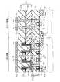
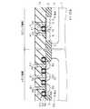
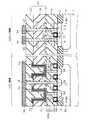
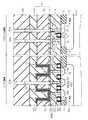
次に図14に示されるように、コンタクトプラグ33の位置に対応して設けられた開口パターン39aと、コンタクトプラグ83aの位置に対応して設けられた開口パターン39bとを有するレジスト38を絶縁膜31上に形成し、かかるレジスト38をマスクに用いて、ストッパ膜17をエッチングストッパとして、層間絶縁膜18,23をエッチングして部分的に除去する。このときのエッチングでは、C4F6とO2とArとの混合ガスを使用する異方性ドライエッチングが採用される。そして、レジスト38を再度マスクに用いて、露出しているストッパ膜17をエッチングして除去する。このときのエッチングでは、CHF3をエッチングガスとして使用する異方性ドライエッチングが採用される。
【0034】
これにより、コンタクトプラグ33に達するコンタクトホール24と、コンタクトプラグ83aに達するコンタクトホール74とが絶縁膜31に形成される。
【0035】
次にレジスト38を除去して、コンタクトホール24,74を充填する、タングステン等から成る高融点金属膜を全面に形成する。そして、例えばCMP法を用いて絶縁膜31の上面上の高融点金属膜を除去する。これにより、図15に示されるように、高融点金属膜から成りコンタクトホール24を充填するコンタクトプラグ25がロジック領域における絶縁膜31に形成され、コンタクトプラグ33とコンタクトプラグ25とが互いに接触する。また、高融点金属膜から成りコンタクトホール74を充填するコンタクトプラグ75がメモリ領域における絶縁膜31に形成され、コンタクトプラグ83aとコンタクトプラグ75とが互いに接触する。
【0036】
次に図16に示されるように、絶縁膜31上に、コンタクトプラグ25と接触させて配線26を形成し、コンタクトプラグ75と接触させてDRAMメモリセルのビット線76を形成する。配線26及びビット線76には例えばアルミ配線が採用される。
【0037】
以上の工程により、メモリ領域にはConcave型MIMキャパシタを備えるメモリデバイスが形成され、ロジック領域にはスタック構造を備えるロジックデバイスが形成される。
【0038】
このように本実施の形態1に係る半導体装置の製造方法では、キャパシタ73と接続されるコンタクトプラグ83bの上端部には、酸化防止用の導電性バリア層82が形成されているため、キャパシタ73の誘電体膜71の形成時にコンタクトプラグ83bの導電性膜66が酸化されることが無い。従って、キャパシタ73とソース・ドレイン領域59との間のコンタクト抵抗を低減できる。更に、ロジック領域ではスタック構造が採用されているため、コンタクトプラグのアスペクト比の増大によるコンタクト不良を低減できる。従って、本実施の形態1のようにキャパシタ73の誘電体膜71の形成時に酸化処理が実行される場合であっても、メモリデバイスでのコンタクト抵抗の低減とロジックデバイスでのコンタクト抵抗の低減とを両立させることが可能となる。
【0039】
なお、本実施の形態1では、DRAMメモリセルのキャパシタ73としてConcave型MIMキャパシタを備える半導体装置の製造方法について説明したが、キャパシタ73として他の構造のMIMキャパシタを備える半導体装置の製造方法にも本発明を適用することができる。例えば、図17に示されるようなサポート付きCylinder型MIMキャパシタや、図18に示されるようなPillar型MIMキャパシタや、図19に示されるような厚膜スタック型MIMキャパシタを備える半導体装置の製造方法に本発明を適用することができる。
【0040】
キャパシタ73としてサポート付きCylinder型MIMキャパシタを採用した場合には、本実施の形態1に係る半導体装置よりも蓄積容量を増加させることができ、Pillar型MIMキャパシタを採用した場合や厚膜スタック型MIMキャパシタを採用した場合には、上部電極72を形成する際の成膜カバレッジが優れるため、本実施の形態1に係る半導体装置よりもキャパシタ73のリーク電流を低減できる。
【0041】
また、Pillar型MIMキャパシタを採用した場合や厚膜スタック型MIMキャパシタを採用した場合には、コンタクトプラグ25,75のアスペクト比を小さくすることができるため、図20や図21に示されるように、コンタクトプラグ25と配線26とを、あるいはコンタクトプラグ75とビット線76とをデュアル・ダマシン法を用いて一体的に形成しても良い。
【0042】
なお、厚膜スタック型MIMキャパシタを採用した場合には、絶縁膜31の層間絶縁膜18は製造過程で除去されるため、図19,21では図示されていない。
【0043】
また、本実施の形態1では、絶縁膜14及び層間絶縁膜18,23に対するエッチングでは、C4F6とO2とArとの混合ガスを使用したが、C5F8やC4F6とO2とArとの混合ガスを使用しても良い。
【0044】
実施の形態2.
上述の実施の形態1では、キャパシタ73と接続されるコンタクトプラグ83bの上端部に導電性バリア層82を設けていたが、キャパシタ73の誘電体膜71の形成時には、コンタクトプラグ83bだけではなく、その周辺のメモリ領域におけるコンタクトプラグ83aも酸化される場合がある。
【0045】
そこで、本実施の形態2では、DRAMメモリセルのビット線76と電気的に接続されるコンタクトプラグ83aの上端部にも導電性バリア層82を形成する場合の製造方法について説明する。
【0046】
図22〜30は本発明の実施の形態2に係る半導体装置の製造方法を工程順に示す断面図である。まず、実施の形態1に係る製造方法を用いて上述の図4に示される構造を得る。そして図22に示されるように、i線露光対応のレジスト35を全面に形成し、メモリ領域を開口する開口パターンをi線を光源として用いた写真製版法によってレジスト35に形成する。そして図23に示されるように、レジスト35をマスクに用いて露出している部分に対してエッチングを実行し、キャパシタ73と電気的に接続される導電性膜66の上端部とビット線76と電気的に接続される導電性膜66の上端部とを選択的に除去する。これにより、メモリ領域における絶縁膜14に凹部81が形成される。このときのエッチングでは、エッチングガスとしてSF6を使用する異方性ドライエッチングが採用される。
【0047】
本実施の形態2では、実施の形態1とは異なり、ビット線76と電気的に接続される導電性膜66をレジストでマスクする必要がないため、レジスト35にはメモリ領域すべてを開口する開口パターンを形成している。従って、本実施の形態2では、実施の形態1で使用したエキシマ露光対応のレジスト30よりも安価なi線露光対応のレジスト35を採用することができる。そして、レジスト35に開口パターンを形成する際には実施の形態1よりも安価な露光装置を使用することができる。
【0048】
次に図24に示されるように、マスクに使用したレジスト35を除去する。そして、窒化チタン、窒化タンタル、あるいは窒化チタンシリサイド等から成り、各凹部81を充填するバリア層材料を全面に形成し、例えばCMP法を用いて凹部81よりも上方のバリア層材料を除去する。これにより、図25に示されるように、各凹部81を充填する導電性バリア層82が絶縁膜14内に形成される。
【0049】
以上の工程により、メモリ領域における絶縁膜14には、互いに隣り合うソース・ドレイン領域59の一方に電気的に接続され、上端部に導電性バリア層82を、それ以外の部分に導電性膜66を有するコンタクトプラグ83aと、互いに隣り合うソース・ドレイン領域59の他方に電気的に接続され、上端部に導電性バリア層82を、それ以外の部分に導電性膜66を有するコンタクトプラグ83bとが形成される。また、ロジック領域における絶縁膜14には、導電性膜16から成るコンタクトプラグ33が形成される。
【0050】
次に図26に示されるように、絶縁膜14及びコンタクトプラグ33,83a,83bの上に、ストッパ膜17及び層間絶縁膜18をこの順で堆積する。そして図27に示されるように、実施の形態1と同様にして開口部69、キャパシタ73及び層間絶縁膜23を順次形成する。なお、図27に示されるキャパシタ73はConcave型MIMキャパシタである。
【0051】
次に図28に示されるように、開口パターン39a,39bを有するレジスト38を絶縁膜31上に形成し、かかるレジスト38をマスクに用いて、層間絶縁膜18,23及びストッパ膜17をエッチングして除去する。これにより、コンタクトプラグ33に達するコンタクトホール24と、コンタクトプラグ83aの導電性バリア層82に達するコンタクトホール74とが絶縁膜31に形成される。
【0052】
次にレジスト38を除去して、図29に示されるように、コンタクトホール24を充填するコンタクトプラグ25と、コンタクトホール74を充填するコンタクトプラグ75とを形成する。これにより、コンタクトプラグ33とコンタクトプラグ25とが互いに接触し、コンタクトプラグ83aの導電性バリア層82とコンタクトプラグ75とが互いに接触する。
【0053】
次に図30に示されるように、絶縁膜31上に配線26及びビット線76を形成する。
【0054】
以上の工程により、メモリ領域にはメモリデバイスが形成され、ロジック領域にはロジックデバイスが形成される。
【0055】
このように本実施の形態2に係る半導体装置の製造方法では、キャパシタ73と接続されるコンタクトプラグ83bの上端部のみならず、ビット線76及びコンタクトプラグ75と電気的に接続されるコンタクトプラグ83aの上端部にも酸化防止用の導電性バリア層82が形成されているため、キャパシタ73の誘電体膜71の形成時にコンタクトプラグ83aの導電性膜66が酸化されることが無い。従って、ビット線76あるいはコンタクトプラグ75とソース・ドレイン領域59との間のコンタクト抵抗を低減できる。
【0056】
なお、本実施の形態2では、DRAMメモリセルのキャパシタ73としてConcave型MIMキャパシタを備える半導体装置の製造方法について説明したが、実施の形態1と同様に、キャパシタ73として他の構造のMIMキャパシタを備える半導体装置の製造方法にも本発明を適用することができる。例えば、図31に示されるようなサポート付きCylinder型MIMキャパシタや、図32に示されるようなPillar型MIMキャパシタや、図33に示されるような厚膜スタック型MIMキャパシタを備える半導体装置の製造方法に本発明を適用することができる。
【0057】
また、Pillar型MIMキャパシタを採用した場合や厚膜スタック型MIMキャパシタを採用した場合には、コンタクトプラグ25,75のアスペクト比を小さくすることができるため、図34や図35に示されるように、コンタクトプラグ25と配線26とを、あるいはコンタクトプラグ75とビット線76とをデュアル・ダマシン法を用いて一体的に形成しても良い。
【0058】
なお、厚膜スタック型MIMキャパシタを採用した場合には、絶縁膜31の層間絶縁膜18は製造過程で除去されるため、図33,35では図示されていない。
【0059】
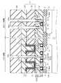
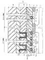
実施の形態3.
上述の実施の形態2では、メモリ領域におけるコンタクトプラグ83a,83bの上端部に導電性バリア層82を設けていたが、キャパシタ73の誘電体膜71の形成時には、メモリ領域だけではなく、ロジック領域におけるコンタクトプラグ33も酸化される場合がある。
【0060】
そこで、本実施の形態2では、ロジック領域におけるコンタクトプラグ33の上端部にも導電性バリア層を形成する場合の製造方法について説明する。
【0061】
図36〜42は本発明の実施の形態3に係る半導体装置の製造方法を工程順に示す断面図である。まず、実施の形態1に係る製造方法を用いて上述の図4に示される構造を得る。そして図36に示されるように、レジストを形成せずに、全面に対してエッチングを行って、メモリ領域における各導電性膜66の上端部とロジック領域における各導電性膜16の上端部とを選択的に除去する。これにより、メモリ領域における絶縁膜14に凹部81が形成され、ロジック領域における絶縁膜14には凹部41が形成される。このときのエッチングでは、エッチングガスとしてSF6を使用する異方性ドライエッチングが採用される。
【0062】
次に、窒化チタン、窒化タンタル、あるいは窒化チタンシリサイド等から成り、各凹部41,81を充填するバリア層材料を全面に形成し、例えばCMP法を用いて凹部41,81よりも上方のバリア層材料を除去する。これにより、図37に示されるように、メモリ領域の各凹部81を充填する導電性バリア層82が絶縁膜14内に形成され、更に、窒化チタン、窒化タンタル、あるいは窒化チタンシリサイド等から成り、ロジック領域の各凹部41を充填する導電性バリア層42が絶縁膜14内に形成される。
【0063】
以上の工程により、メモリ領域における絶縁膜14には、上端部に導電性バリア層82を有するコンタクトプラグ83aと、同じく上端部に導電性バリア層82を有するコンタクトプラグ83bとが形成される。また、ロジック領域における絶縁膜14には、上端部に導電性バリア層42を、それ以外の部分には導電性膜16を有するコンタクトプラグ33が形成される。なお、導電性バリア層82と同様に導電性バリア層42も導電性膜16,66よりも導電率が低い。
【0064】
次に図38に示されるように、絶縁膜14及びコンタクトプラグ33,83a,83bの上に、ストッパ膜17及び層間絶縁膜18をこの順で堆積する。そして図39に示されるように、実施の形態1と同様にして開口部69、キャパシタ73及び層間絶縁膜23を順次形成する。なお、図39に示されるキャパシタ73はConcave型MIMキャパシタである。
【0065】
次に図40に示されるように、開口パターン39a,39bを有するレジスト38を絶縁膜31上に形成し、かかるレジスト38をマスクに用いて、層間絶縁膜18,23及びストッパ膜17をエッチングして除去する。これにより、コンタクトプラグ33の導電性バリア層42に達するコンタクトホール24と、コンタクトプラグ83aの導電性バリア層82に達するコンタクトホール74とが絶縁膜31に形成される。
【0066】
次にレジスト38を除去して、図41に示されるように、コンタクトホール24を充填するコンタクトプラグ25と、コンタクトホール74を充填するコンタクトプラグ75とを形成する。これにより、コンタクトプラグ33の導電性バリア層42とコンタクトプラグ25とが互いに接触し、コンタクトプラグ83aの導電性バリア層82とコンタクトプラグ75とが互いに接触する。
【0067】
次に図42に示されるように、絶縁膜31上に配線26及びビット線76を形成する。
【0068】
以上の工程により、メモリ領域にはメモリデバイスが形成され、ロジック領域にはロジックデバイスが形成される。
【0069】
このように本実施の形態3に係る半導体装置の製造方法では、メモリ領域におけるコンタクトプラグ83a,83bの上端部のみならず、ロジック領域における下層のコンタクトプラグ33の上端部にも酸化防止用の導電性バリア層42が形成されているため、キャパシタ73の誘電体膜71の形成時にコンタクトプラグ33の導電性膜16が酸化されることが無い。従って、ロジック領域における上層のコンタクトプラグ25とソース・ドレイン領域9との間のコンタクト抵抗を更に低減できる。
【0070】
なお、本実施の形態3では、DRAMメモリセルのキャパシタ73としてConcave型MIMキャパシタを備える半導体装置の製造方法について説明したが、実施の形態1,2と同様に、キャパシタ73として他の構造のMIMキャパシタを備える半導体装置の製造方法にも本発明を適用することができる。例えば、図43に示されるようなサポート付きCylinder型MIMキャパシタや、図44に示されるようなPillar型MIMキャパシタや、図45に示されるような厚膜スタック型MIMキャパシタを備える半導体装置の製造方法に本発明を適用することができる。
【0071】
また、Pillar型MIMキャパシタを採用した場合や厚膜スタック型MIMキャパシタを採用した場合には、コンタクトプラグ25,75のアスペクト比を小さくすることができるため、図46や図47に示されるように、コンタクトプラグ25と配線26とを、あるいはコンタクトプラグ75とビット線76とをデュアル・ダマシン法を用いて一体的に形成しても良い。
【0072】
なお、厚膜スタック型MIMキャパシタを採用した場合には、絶縁膜31の層間絶縁膜18は製造過程で除去されるため、図45,47では図示されていない。
【0073】
実施の形態4.
上述の実施の形態3に係る製造方法で製造された半導体装置では、図42に示されるように、コンタクトプラグ33,83aの上端部には酸化防止膜として作用する導電性バリア層42,82が残存したままであったが、キャパシタ73形成後には、導電性バリア層42,82は不要のため除去しても良い。本実施の形態4では、キャパシタ73形成後に導電性バリア層42,82を除去する方法について説明する。
【0074】
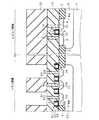
図48〜50は本発明の実施の形態4に係る半導体装置の製造方法を工程順に示す断面図である。まず、実施の形態3に係る製造方法を用いて図39に示される構造を得る。そして図48に示されるように、開口パターン39a,39bを有するレジスト38を絶縁膜31上に形成し、かかるレジスト38をマスクに用いて、ストッパ膜17をエッチングストッパとして、層間絶縁膜18,23をエッチングして除去する。このときのエッチングでは、C4F6とO2とArとの混合ガスを使用する異方性ドライエッチングが採用される。そして、使用するエッチングガスを変更し、レジスト38を再度マスクに用いて露出しているストッパ膜17をエッチングして除去する。このときのエッチングでは、CHF3をエッチングガスとして使用する異方性ドライエッチングが採用される。
【0075】
これにより、コンタクトプラグ83aに達するコンタクトホール74と、コンタクトプラグ33に達するコンタクトホール24とが絶縁膜31に形成される。
【0076】
次に、再度使用するエッチングガスを変更し、レジスト38をマスクに用いて露出している導電性バリア層42,82をエッチングして除去する。このときのエッチングには、Cl2とCHF3との混合ガスを使用する異方性ドライエッチングが採用される。
【0077】
これにより、コンタクトプラグ83aの導電性膜66を露出しつつ、コンタクトホール74と連通する凹部93がメモリ領域における絶縁膜14に形成される。同時に、コンタクトプラグ33の導電性膜16を露出しつつ、コンタクトホール24と連通する凹部43がロジック領域における絶縁膜14に形成される。
【0078】
次にレジスト38を除去して、凹部43,93及びコンタクトホール24,74を充填する、タングステン等から成る高融点金属膜を全面に形成する。そして、例えばCMP法を用いて絶縁膜31の上面上の高融点金属膜を除去する。これにより、図49に示されるように、コンタクトホール24及び凹部43を充填するコンタクトプラグ25がロジック領域における絶縁膜14,31に形成され、コンタクトプラグ33の導電性膜16とコンタクトプラグ25とが互いに接触する。また、コンタクトホール74及び凹部93を充填するコンタクトプラグ75がメモリ領域における絶縁膜14,31に形成され、コンタクトプラグ83aの導電性膜66とコンタクトプラグ75とが互いに接触する。その後、図50に示されるように、配線26とビット線76とを絶縁膜31上に形成し、メモリ・ロジック混載型の半導体装置が完成する。
【0079】
このように、本実施の形態4に係る半導体装置の製造方法では、キャパシタ73の形成後に、メモリ領域におけるコンタクトプラグ83aの上端部に設けられた導電性バリア層82を除去しているため、上層のコンタクトプラグ75は下層のコンタクトプラグ83aの導電性膜66と接触する。また、導電性膜66は導電性バリア層82よりも導電率が高い。従って、上層のコンタクトプラグ75が下層のコンタクトプラグ83aの導電性バリア層82に接触して形成される実施の形態3に係る製造方法よりも、上層のコンタクトプラグ75と下層のコンタクトプラグ83aとの間の接触抵抗を低減できる。その結果、コンタクトプラグ75あるいはビット線76とソース・ドレイン領域59との間のコンタクト抵抗を更に低減することができる。
【0080】
また、キャパシタ73の形成後に、ロジック領域におけるコンタクトプラグ33の上端部に設けられた導電性バリア層42を除去しているため、上層のコンタクトプラグ25は下層のコンタクトプラグ33の導電性膜16と接触する。また、導電性膜16は導電性バリア層42よりも導電率が高い。従って、上層のコンタクトプラグ25が下層のコンタクトプラグ33の導電性バリア層42に接触して形成される実施の形態3に係る製造方法よりも、上層のコンタクトプラグ25と下層のコンタクトプラグ33との間の接触抵抗を低減できる。その結果、コンタクトプラグ25とソース・ドレイン領域9との間のコンタクト抵抗を更に低減することができる。
【0081】
また、本実施の形態4では、絶縁膜31にコンタクトホール24,74を形成する際に使用したレジスト38を用いつつ、エッチングガスを切り替えて導電性バリア層42,82を除去しているため、少ない工程数で導電性バリア層42,82を除去することができる。
【0082】
実施の形態5.
図51は本発明の実施の形態5に係る半導体装置の構造を示す断面図である。本実施の形態5に係る半導体装置は、上述の図42に示される構造からコンタクトプラグ25の形状を変形したものである。従って、本実施の形態5に係る半導体装置に関して、実施の形態1〜4で述べた内容については説明を省略する場合がある。
【0083】
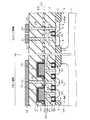
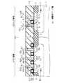
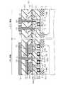
図51に示されるように、本実施の形態5に係る半導体装置は、半導体基板1と、半導体基板1上に設けられた絶縁膜14と、絶縁膜14内に設けられたコンタクトプラグ33,83a,83bと、コンタクトプラグ83bと接触させて絶縁膜14上に設けられたキャパシタ73と、キャパシタ73を覆って絶縁膜14上に設けられた絶縁膜31と、絶縁膜31内に設けられたコンタクトプラグ25,75と、絶縁膜31上に設けられた配線26及びビット線76とを備えている。
【0084】
半導体基板1の上面内には素子分離絶縁膜2が設けられている。また、ロジック形成領域における半導体基板1の上面内にはウェル領域3が設けられており、メモリ形成領域における半導体基板1の上面内にはウェル領域53が設けられている。
【0085】
ウェル領域3の上面内には、互いに所定距離を成す複数のソース・ドレイン領域9が設けられており、ウェル領域53の上面内には、互いに所定距離を成す複数のソース・ドレイン領域59が設けられている。
【0086】
互いに隣り合うソース・ドレイン領域9の間のウェル領域3の上面上にはゲート構造11が設けられており、互いに隣り合うソース・ドレイン領域59の間のウェル領域53の上面上にはゲート構造61が設けられている。
【0087】
ゲート構造11のゲート電極6の上面上と、ゲート構造61のゲート電極56の上面上にはシリサイド膜12が設けられている。また、各ソース・ドレイン領域9,59上にもシリサイド膜12が設けられている。
【0088】
コンタクトプラグ33,83a,83bのそれぞれは、その上面が絶縁膜14から露出している。そして、コンタクトプラグ83bは、互いに隣り合うソース・ドレイン領域59の一方とシリサイド膜12を介して電気的に接続されており、コンタクトプラグ83aは互いに隣り合うソース・ドレイン領域59の他方とシリサイド膜12を介して電気的に接続されている。また、コンタクトプラグ33はソース・ドレイン領域9とシリサイド膜12を介して電気的に接続されている。
【0089】
メモリ領域におけるコンタクトプラグ75はコンタクトプラグ83aの導電性バリア層82の上面と接触しており、その上面が絶縁膜31から露出している。そして、ビット線76はコンタクトプラグ75と接触している。
【0090】
ロジック領域におけるコンタクトプラグ25は、その上面が絶縁膜31から露出しており、配線26と接触している。また、コンタクトプラグ25は絶縁膜14内に延びており、コンタクトプラグ33の導電性バリア層42と接触し、更にその導電性膜16の上端部の側面の一部に接触している。
【0091】
このように本実施の形態5に係る半導体装置によれば、ロジック領域におけるコンタクトプラグ33が酸化防止用の導電性バリア層42を備えている場合であっても、上層のコンタクトプラグ25は、下層のコンタクトプラグ33の導電性バリア層42のみならず、それよりも導電率の高い導電性膜16と接触している。そのため、上述の図42に示される半導体装置のように、上層のコンタクトプラグ25が導電性バリア層42を介して導電性膜16と電気的に接続されている半導体装置よりも、ロジック領域における上層のコンタクトプラグ25と半導体基板1に設けられたソース・ドレイン領域9との間のコンタクト抵抗を低減することができる。
【0092】
更に、キャパシタ73と接触するコンタクトプラグ83bの上端部には導電性バリア層82が設けられているため、キャパシタ73の誘電体膜71の形成時に、コンタクトプラグ83bの導電性膜66が酸化されることを防止することができる。従って、キャパシタ73の誘電体膜71の形成時に酸化処理が実行される場合であっても、メモリデバイスでのコンタクト抵抗の低減とロジックデバイスでのコンタクト抵抗の低減とを両立させることが可能となる。
【0093】
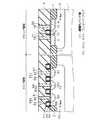
次に図51に示す半導体装置の製造方法について、図52〜55を参照して説明する。まず、実施の形態3に係る製造方法を用いて上述の図39に示される構造を得る。次に図52に示されるように、レジスト38を絶縁膜31上に形成する。
【0094】
そして図53に示されるように、コンタクトプラグ33,83aの位置に対応させて開口パターン39a,39bをそれぞれレジスト38に形成する。このとき、コンタクトプラグ33の上方に設けられる開口パターン39aに関しては、コンタクトプラグ33に対するアライメントを意図的に少しずらして形成する。そのため、図53に示されるように、開口パターン39aは、コンタクトプラグ33の直上のみならず絶縁膜14の直上にも形成されている。
【0095】
なお、コンタクトプラグ83aの上方に設けられる開口パターン39bに関しては、コンタクトプラグ83aに対するアライメントを意図的にはずらさずに形成し、開口パターン39bがコンタクトプラグ83aの直上のみに位置するように形成する。また、本実施の形態5では、開口パターン39aの径をコンタクトプラグ33の径とほぼ同じに設定し、開口パターン39bの径をコンタクトプラグ83aの径とほぼ同じに設定する。
【0096】
次に図54に示されるように、開口パターン39a,39bを有するレジスト38をマスクに用いて、ストッパ膜17をエッチングストッパとして、層間絶縁膜18,23をエッチングして部分的に除去する。このときのエッチングでは、C4F6とO2とArとの混合ガスを使用する異方性ドライエッチングが採用される。
【0097】
そして、レジスト38を再度マスクに用いつつ、CHF3をエッチングガスとして使用する異方性ドライエッチング法を用いて、露出しているストッパ膜17をエッチングして除去し、コンタクトプラグ33に達するコンタクトホール24と、コンタクトプラグ83aに達するコンタクトホール74とを絶縁膜31に形成する。このとき、ストッパ膜17に対して所定量のオーバーエッチングを実行し、コンタクトホール24を絶縁膜14内にまで延長することによって、コンタクトプラグ33の導電性膜16の側面を露出させる。
【0098】
上述のように、コンタクトプラグ33に対する開口パターン39aの重ね合わせ位置がずれているため、開口パターン39aはコンタクトプラグ33の直上のみならず、絶縁膜14の直上にも位置している。そのため、ストッパ膜17に対してオーバーエッチングを実行することによって、ロジック領域では絶縁膜14もエッチングされる。従って、ストッパ膜17に対して所定量のオーバーエッチングを行うことによって、コンタクトプラグ33の導電性バリア層42のみならず、その導電性膜16の上端部の側面の一部も露出する。
【0099】
なお、開口パターン39bは、コンタクトプラグ83aの直上にしか位置していないため、メモリ領域では絶縁膜14はエッチングされない。また、ストッパ膜17を除去する際に使用されるエッチングガスでは、コンタクトプラグ83aの導電性バリア層82はほとんどエッチングされないため、コンタクトホール74の形成後では、コンタクトプラグ83aの上端部に導電性バリア層82が残存したままである。
【0100】
次に図55に示されるように、コンタクトホール24を充填するコンタクトプラグ25と、コンタクトホール74を充填するコンタクトプラグ75とを形成する。これにより、コンタクトプラグ25は、絶縁膜31内のみならず絶縁膜14内にも形成され、コンタクトプラグ33の導電性バリア層42と、その導電性膜16の側面の上端部の一部と接触する。その後、配線26及びビット線76を絶縁膜31上に形成することにより図51に示される半導体装置が得られる。
【0101】
このように本実施の形態5に係る半導体装置の製造方法によれば、ロジック領域におけるコンタクトプラグ33の上端部に酸化防止用の導電性バリア層42を形成した場合であっても、上層のコンタクトプラグ25は、下層のコンタクトプラグ33の導電性バリア層42のみならず、それよりも導電率の高い導電性膜16と接触するようになる。そのため、上述の実施の形態3に係る半導体装置の製造方法のように、上層のコンタクトプラグ25が導電性バリア層42を介して導電性膜16と電気的に接続されて形成される場合よりも、ロジック領域における上層のコンタクトプラグ25と半導体基板1に設けられたソース・ドレイン領域9との間のコンタクト抵抗を低減することができる。
【0102】
更に、コンタクトプラグ83bの上端部には導電性バリア層82が設けられているため、キャパシタ73の誘電体膜71の形成時に、コンタクトプラグ83bの導電性膜66が酸化されることを防止することができる。従って、メモリデバイスでのコンタクト抵抗の低減とロジックデバイスでのコンタクト抵抗の低減とを両立させることが可能となる。
【0103】
なお本実施の形態5では、メモリ領域における上層のコンタクトプラグ75はコンタクトプラグ83aの導電性バリア層82だけと接触し導電性膜66とは接触していなかったが、図56に示される半導体装置のように、コンタクトプラグ75を絶縁膜14内にまで延ばして、下層のコンタクトプラグ83aの導電性膜66の側面にも接触させても良い。
【0104】
このように、上層のコンタクトプラグ75を、下層のコンタクトプラグ83aの導電性膜66と接触させることによって、メモリ領域におけるコンタクトプラグ83aが酸化防止用の導電性バリア層82を備えている場合であっても、上層のコンタクトプラグ75あるいはビット線76と半導体基板1に設けられたソース・ドレイン領域59との間のコンタクト抵抗を低減することができる。
【0105】
以下に図56に示される半導体装置の製造方法について、図57,58を参照して説明する。
【0106】
まず、実施の形態3に係る製造方法を用いて上述の図39に示される構造を得る。次に図57に示されるように、レジスト38を絶縁膜31上に形成する。そして、コンタクトプラグ33,83aの位置に対応させて開口パターン39a,39bをそれぞれレジスト38に形成する。このとき、コンタクトプラグ33の上方に設けられる開口パターン39aと同様に、コンタクトプラグ83aの上方に設けられる開口パターン39bに関しても、コンタクトプラグ83aに対するアライメントを意図的に少しずらして形成する。そのため、開口パターン39bは、コンタクトプラグ83aの直上のみならず、絶縁膜14の直上にも位置している。
【0107】
次に図58に示されるように、開口パターン39a,39bを有するレジスト38をマスクに用いて、ストッパ膜17をエッチングストッパとして、層間絶縁膜18,23をエッチングして部分的に除去する。
【0108】
そして、レジスト38を再度マスクに用いつつ、CHF3をエッチングガスとして使用する異方性ドライエッチング法を用いて、露出しているストッパ膜17をエッチングして除去し、コンタクトホール24,74を絶縁膜31に形成する。このとき、ストッパ膜17に対して所定量のオーバーエッチングを実行し、コンタクトホール24,74を絶縁膜14内にまで延長することによって、コンタクトプラグ33の導電性膜16の側面を露出させるとともに、コンタクトプラグ83aの導電性膜66の側面を露出させる。
【0109】
上述のように、コンタクトプラグ83aに対する開口パターン39bの重ね合わせ位置がずれているため、開口パターン39bはコンタクトプラグ83aの直上のみならず、絶縁膜14の直上にも位置している。そのため、ストッパ膜17に対してオーバーエッチングを実行することによって、ロジック領域の絶縁膜14のみならず、メモリ領域の絶縁膜14もエッチングされる。従って、ストッパ膜17に対して所定量のオーバーエッチングを行うことによって、コンタクトプラグ83aの導電性バリア層82のみならず、その導電性膜66の上端部の側面の一部も露出する。
【0110】
次に、コンタクトホール24を充填するコンタクトプラグ25と、コンタクトホール74を充填するコンタクトプラグ75とを形成する。これにより、コンタクトプラグ25と同様に、コンタクトプラグ75は、絶縁膜31内のみならず絶縁膜14内にも形成され、コンタクトプラグ83aの導電性バリア層82と、その導電性膜66の上端部の側面の一部と接触する。そして、配線26及びビット線76を絶縁膜31上に形成することにより図56に示される半導体装置が得られる。
【0111】
このように、メモリ領域におけるコンタクトプラグ83aの上端部に酸化防止用の導電性バリア層82を形成した場合であっても、上層のコンタクトプラグ75は、下層のコンタクトプラグ83aの導電性バリア層82のみならず、それよりも導電率の高い導電性膜66と接触するようになる。そのため、メモリ領域における上層のコンタクトプラグ75と半導体基板1に設けられたソース・ドレイン領域59との間のコンタクト抵抗を低減することができる。
【0112】
また本実施の形態5では、DRAMメモリセルのキャパシタ73としてConcave型MIMキャパシタを備える半導体装置及びその製造方法について説明したが、キャパシタ73として他の構造のMIMキャパシタを備える半導体装置及びその製造方法にも本発明を適用することができる。例えば、図59に示されるようなサポート付きCylinder型MIMキャパシタや、図60に示されるようなPillar型MIMキャパシタや、図61に示されるような厚膜スタック型MIMキャパシタを備える半導体装置及びその製造方法に本発明を適用することができる。
【0113】
また、Pillar型MIMキャパシタを採用した場合や厚膜スタック型MIMキャパシタを採用した場合には、コンタクトプラグ25,75のアスペクト比を小さくすることができるため、図62や図63に示されるように、コンタクトプラグ25と配線26とを、あるいはコンタクトプラグ75とビット線76とをデュアル・ダマシン法を用いて一体的に形成しても良い。
【0114】
なお、厚膜スタック型MIMキャパシタを採用した場合には、絶縁膜31の層間絶縁膜18は製造過程で除去されるため、図61,63では図示されていない。
【0115】
実施の形態6.
図64は本発明の実施の形態6に係る半導体装置の構造を示す断面図である。本実施の形態6に係る半導体装置は、上述の実施の形態5に係る半導体装置において、コンタクトプラグ25の形状を変形したものである。
【0116】
図64に示されるように、本実施の形態6に係る半導体装置が備えるコンタクトプラグ25は、その上面が絶縁膜31から露出しており、配線26と接触している。また、コンタクトプラグ25は、その径がコンタクトプラグ33の径よりも大きく、絶縁膜14内に延びている。そしてコンタクトプラグ25は、コンタクトプラグ33の導電性バリア層42と接触しており、更にその導電性膜16の側面の上端部の全周囲と接触している。その他の構造については、実施の形態5に係る半導体装置と同様のためその説明は省略する。
【0117】
このように本実施の形態6に係る半導体装置によれば、ロジック領域におけるコンタクトプラグ33が酸化防止用の導電性バリア層42を備えている場合であっても、上層のコンタクトプラグ25は、下層のコンタクトプラグ33の導電性バリア層42のみならず、それよりも導電率の高い導電性膜16の上端部の側面の全周囲と接触している。そのため、コンタクトプラグ25が導電性膜16の上端部の側面の一部しか接触していない上述の実施の形態5に係る半導体装置よりも、ロジック領域における上層のコンタクトプラグ25と半導体基板1に設けられたソース・ドレイン領域9との間のコンタクト抵抗を低減することができる。
【0118】
次に図64に示される半導体装置の製造方法について、図65〜67を参照して説明する。なお、実施の形態5に係る半導体装置の製造方法と同じ内容についてはその説明を省略する。
【0119】
まず、実施の形態3に係る製造方法を用いて上述の図39に示される構造を得る。次に図65に示されるように、レジスト38を絶縁膜31上に形成する。
【0120】
そして、コンタクトプラグ33,83aの位置に対応させて開口パターン39a,39bをそれぞれレジスト38に形成する。このとき、コンタクトプラグ33の上方に設けられる開口パターン39aに関しては、その径をコンタクトプラグ33の径よりも大きく設定し、コンタクトプラグ33に対するアライメントは意図的にはずらさないようにする。そのため、図65に示されるように、開口パターン39aは、コンタクトプラグ33の直上のみならず、コンタクトプラグ33を取り囲む絶縁膜14の一部の直上にも形成されている。
【0121】
次に図66に示されるように、開口パターン39a,39bを有するレジスト38をマスクに用いて、ストッパ膜17をエッチングストッパとして、層間絶縁膜18,23をエッチングして部分的に除去する。
【0122】
そして、レジスト38を再度マスクに用いつつ、CHF3をエッチングガスとして使用する異方性ドライエッチング法を用いて、露出しているストッパ膜17をエッチングして除去し、コンタクトプラグ33に達するコンタクトホール24と、コンタクトプラグ83aに達するコンタクトホール74とを絶縁膜31に形成する。このとき、ストッパ膜17に対して所定量のオーバーエッチングを実行し、コンタクトホール24を絶縁膜14内にまで延長することによって、コンタクトプラグ33における導電性膜16の側面の上端部の全周囲を露出させる。
【0123】
上述のように、開口パターン39aの径はコンタクトプラグ33の径よりも大きいため、開口パターン39aはコンタクトプラグ33の直上のみならず、コンタクトプラグ33を取り囲む絶縁膜14の一部の直上にも位置している。従って、ストッパ膜17に対して所定量のオーバーエッチングを行うことによって絶縁膜14がエッチングされ、コンタクトプラグ33の導電性バリア層42のみならず、その導電性膜16の側面の上端部の全周囲も露出する。
【0124】
次に図67に示されるように、コンタクトホール24を充填するコンタクトプラグ25と、コンタクトホール74を充填するコンタクトプラグ75とを形成する。これにより、コンタクトプラグ25は、絶縁膜31内のみならず絶縁膜14内にも形成され、コンタクトプラグ33の導電性バリア層42と、その導電性膜16の側面の上端部の全周囲と接触する。その後、配線26及びビット線76を絶縁膜31上に形成することにより図64に示される半導体装置が得られる。
【0125】
このように本実施の形態6に係る半導体装置の製造方法によれば、ロジック領域におけるコンタクトプラグ33の上端部に酸化防止用の導電性バリア層42を形成した場合であっても、上層のコンタクトプラグ25は、下層のコンタクトプラグ33の導電性バリア層42のみならず、それよりも導電率の高い導電性膜16の側面の上端部の全周囲と接触するようになる。そのため、上述の実施の形態5に係る半導体装置の製造方法よりも、ロジック領域における上層のコンタクトプラグ25と半導体基板1に設けられたソース・ドレイン領域9との間のコンタクト抵抗を低減することができる。
【0126】
なお本実施の形態6では、上述の実施の形態5と同様に、メモリ領域における上層のコンタクトプラグ75はコンタクトプラグ83aの導電性バリア層82だけと接触し導電性膜66とは接触していなかったが、図68に示される半導体装置のように、コンタクトプラグ75を絶縁膜14内にまで延ばして、下層のコンタクトプラグ83aにおける導電性膜66の上端部の側面の全周囲と接触させても良い。
【0127】
このように、メモリ領域における上層のコンタクトプラグ75を、下層のコンタクトプラグ83aにおける導電性膜66の側面の全周囲と接触させることによって、メモリ領域におけるコンタクトプラグ83aが酸化防止用の導電性バリア層82を備えている場合であっても、上層のコンタクトプラグ75あるいはビット線76と半導体基板1に設けられたソース・ドレイン領域59との間のコンタクト抵抗を更に低減することができる。
【0128】
以下に図68に示される半導体装置の製造方法について、図69,70を参照して説明する。
【0129】
まず、実施の形態3に係る製造方法を用いて上述の図39に示される構造を得る。次に図69に示されるように、レジスト38を絶縁膜31上に形成する。そして、コンタクトプラグ33,83aの位置に対応させて開口パターン39a,39bをそれぞれレジスト38に形成する。このとき、コンタクトプラグ33の上方に設けられる開口パターン39aと同様に、コンタクトプラグ83aの上方に設けられる開口パターン39bに関しても、その径をコンタクトプラグ83aの径よりも大きく設定し、コンタクトプラグ83aに対するアライメントは意図的にはずらさずに形成する。そのため、開口パターン39bは、コンタクトプラグ83aの直上のみならず、コンタクトプラグ83aを取り囲む絶縁膜14の一部の直上にも形成される。
【0130】
次に図70に示されるように、開口パターン39a,39bを有するレジスト38をマスクに用いて、ストッパ膜17をエッチングストッパとして、層間絶縁膜18,23をエッチングして部分的に除去する。
【0131】
そして、レジスト38を再度マスクに用いつつ、CHF3をエッチングガスとして使用する異方性ドライエッチング法を用いて、露出しているストッパ膜17をエッチングして除去し、コンタクトホール24,74を絶縁膜31に形成する。このとき、ストッパ膜17に対して所定量のオーバーエッチングを実行し、コンタクトホール24,74を絶縁膜14内にまで延長することによって、コンタクトプラグ33における導電性膜16の上端部の側面の全周囲を露出させるとともに、コンタクトプラグ83aにおける導電性膜66の上端部の側面の全周囲を露出させる。
【0132】
上述のように、開口パターン39bの径はコンタクトプラグ83aの径よりも大きいため、開口パターン39bはコンタクトプラグ83aの直上のみならず、それを取り囲む絶縁膜14の一部の直上にも位置している。従って、ストッパ膜17に対して所定量のオーバーエッチングを行うことによって、コンタクトプラグ83aの導電性バリア層82のみならず、その導電性膜66の上端部の側面の全周囲も露出する。
【0133】
次に、コンタクトホール24を充填するコンタクトプラグ25と、コンタクトホール74を充填するコンタクトプラグ75とを形成する。これにより、コンタクトプラグ25と同様に、コンタクトプラグ75は、絶縁膜31内のみならず絶縁膜14内にも形成され、コンタクトプラグ83aの導電性バリア層82と、その導電性膜66の上端部の側面の全周囲と接触する。その後、配線26及びビット線76を絶縁膜31上に形成することにより図68に示される半導体装置が得られる。
【0134】
このように、メモリ領域におけるコンタクトプラグ83aの上端部に酸化防止用の導電性バリア層82を形成した場合であっても、上層のコンタクトプラグ75は、下層のコンタクトプラグ83aの導電性バリア層82のみならず、それよりも導電率の高い導電性膜66の上端部の側面の全周囲と接触するようになる。そのため、メモリ領域における上層のコンタクトプラグ75と半導体基板1に設けられたソース・ドレイン領域59との間のコンタクト抵抗を更に低減することができる。
【0135】
また本実施の形態6では、DRAMメモリセルのキャパシタ73としてConcave型MIMキャパシタを備える半導体装置及びその製造方法について説明したが、キャパシタ73として他の構造のMIMキャパシタを備える半導体装置及びその製造方法にも本発明を適用することができる。例えば、図71に示されるようなサポート付きCylinder型MIMキャパシタや、図72に示されるようなPillar型MIMキャパシタや、図73に示されるような厚膜スタック型MIMキャパシタを備える半導体装置及びその製造方法に本発明を適用することができる。
【0136】
また、Pillar型MIMキャパシタを採用した場合や厚膜スタック型MIMキャパシタを採用した場合には、コンタクトプラグ25,75のアスペクト比を小さくすることができるため、図74や図75に示されるように、コンタクトプラグ25と配線26とを、あるいはコンタクトプラグ75とビット線76とをデュアル・ダマシン法を用いて一体的に形成しても良い。
【0137】
なお、厚膜スタック型MIMキャパシタを採用した場合には、絶縁膜31の層間絶縁膜18は製造過程で除去されるため、図73,75では図示されていない。
【0138】
【発明の効果】
この発明に係る半導体装置の製造方法によれば、MIMキャパシタと接続される第1のコンタクトプラグには第1の導電性バリア層が形成されているため、MIMキャパシタの誘電体膜の形成時に第1のコンタクトプラグの第1の導電性膜が酸化されることが無い。従って、MIMキャパシタとメモリ領域における半導体基板との間のコンタクト抵抗を低減できる。更に、ロジック領域ではスタック構造が採用されているため、コンタクトプラグのアスペクト比の増大によるコンタクト不良を低減できる。従って、MIMキャパシタの誘電体膜の形成時に酸化処理が実行される場合であっても、メモリデバイスでのコンタクト抵抗の低減とロジックデバイスでのコンタクト抵抗の低減とを両立させることが可能となる。
【図面の簡単な説明】
【図1】 本発明の実施の形態1に係る半導体装置の製造方法を工程順に示す断面図である。
【図2】 本発明の実施の形態1に係る半導体装置の製造方法を工程順に示す断面図である。
【図3】 本発明の実施の形態1に係る半導体装置の製造方法を工程順に示す断面図である。
【図4】 本発明の実施の形態1に係る半導体装置の製造方法を工程順に示す断面図である。
【図5】 本発明の実施の形態1に係る半導体装置の製造方法を工程順に示す断面図である。
【図6】 本発明の実施の形態1に係る半導体装置の製造方法を工程順に示す断面図である。
【図7】 本発明の実施の形態1に係る半導体装置の製造方法を工程順に示す断面図である。
【図8】 本発明の実施の形態1に係る半導体装置の製造方法を工程順に示す断面図である。
【図9】 本発明の実施の形態1に係る半導体装置の製造方法を工程順に示す断面図である。
【図10】 本発明の実施の形態1に係る半導体装置の製造方法を工程順に示す断面図である。
【図11】 本発明の実施の形態1に係る半導体装置の製造方法を工程順に示す断面図である。
【図12】 本発明の実施の形態1に係る半導体装置の製造方法を工程順に示す断面図である。
【図13】 本発明の実施の形態1に係る半導体装置の製造方法を工程順に示す断面図である。
【図14】 本発明の実施の形態1に係る半導体装置の製造方法を工程順に示す断面図である。
【図15】 本発明の実施の形態1に係る半導体装置の製造方法を工程順に示す断面図である。
【図16】 本発明の実施の形態1に係る半導体装置の製造方法を工程順に示す断面図である。
【図17】 本発明の実施の形態1に係る発明で製造可能な半導体装置の構造を示す断面図である。
【図18】 本発明の実施の形態1に係る発明で製造可能な半導体装置の構造を示す断面図である。
【図19】 本発明の実施の形態1に係る発明で製造可能な半導体装置の構造を示す断面図である。
【図20】 本発明の実施の形態1に係る発明で製造可能な半導体装置の構造を示す断面図である。
【図21】 本発明の実施の形態1に係る発明で製造可能な半導体装置の構造を示す断面図である。
【図22】 本発明の実施の形態2に係る半導体装置の製造方法を工程順に示す断面図である。
【図23】 本発明の実施の形態2に係る半導体装置の製造方法を工程順に示す断面図である。
【図24】 本発明の実施の形態2に係る半導体装置の製造方法を工程順に示す断面図である。
【図25】 本発明の実施の形態2に係る半導体装置の製造方法を工程順に示す断面図である。
【図26】 本発明の実施の形態2に係る半導体装置の製造方法を工程順に示す断面図である。
【図27】 本発明の実施の形態2に係る半導体装置の製造方法を工程順に示す断面図である。
【図28】 本発明の実施の形態2に係る半導体装置の製造方法を工程順に示す断面図である。
【図29】 本発明の実施の形態2に係る半導体装置の製造方法を工程順に示す断面図である。
【図30】 本発明の実施の形態2に係る半導体装置の製造方法を工程順に示す断面図である。
【図31】 本発明の実施の形態2に係る発明で製造可能な半導体装置の構造を示す断面図である。
【図32】 本発明の実施の形態2に係る発明で製造可能な半導体装置の構造を示す断面図である。
【図33】 本発明の実施の形態2に係る発明で製造可能な半導体装置の構造を示す断面図である。
【図34】 本発明の実施の形態2に係る発明で製造可能な半導体装置の構造を示す断面図である。
【図35】 本発明の実施の形態2に係る発明で製造可能な半導体装置の構造を示す断面図である。
【図36】 本発明の実施の形態3に係る半導体装置の製造方法を工程順に示す断面図である。
【図37】 本発明の実施の形態3に係る半導体装置の製造方法を工程順に示す断面図である。
【図38】 本発明の実施の形態3に係る半導体装置の製造方法を工程順に示す断面図である。
【図39】 本発明の実施の形態3に係る半導体装置の製造方法を工程順に示す断面図である。
【図40】 本発明の実施の形態3に係る半導体装置の製造方法を工程順に示す断面図である。
【図41】 本発明の実施の形態3に係る半導体装置の製造方法を工程順に示す断面図である。
【図42】 本発明の実施の形態3に係る半導体装置の製造方法を工程順に示す断面図である。
【図43】 本発明の実施の形態3に係る発明で製造可能な半導体装置の構造を示す断面図である。
【図44】 本発明の実施の形態3に係る発明で製造可能な半導体装置の構造を示す断面図である。
【図45】 本発明の実施の形態3に係る発明で製造可能な半導体装置の構造を示す断面図である。
【図46】 本発明の実施の形態3に係る発明で製造可能な半導体装置の構造を示す断面図である。
【図47】 本発明の実施の形態3に係る発明で製造可能な半導体装置の構造を示す断面図である。
【図48】 本発明の実施の形態4に係る半導体装置の製造方法を工程順に示す断面図である。
【図49】 本発明の実施の形態4に係る半導体装置の製造方法を工程順に示す断面図である。
【図50】 本発明の実施の形態4に係る半導体装置の製造方法を工程順に示す断面図である。
【図51】 本発明の実施の形態5に係る半導体装置の構造を示す断面図である。
【図52】 本発明の実施の形態5に係る半導体装置の製造方法を工程順に示す断面図である。
【図53】 本発明の実施の形態5に係る半導体装置の製造方法を工程順に示す断面図である。
【図54】 本発明の実施の形態5に係る半導体装置の製造方法を工程順に示す断面図である。
【図55】 本発明の実施の形態5に係る半導体装置の製造方法を工程順に示す断面図である。
【図56】 本発明の実施の形態5に係る半導体装置の変形例の構造を示す断面図である。
【図57】 本発明の実施の形態5に係る半導体装置の変形例の製造方法を工程順に示す断面図である。
【図58】 本発明の実施の形態5に係る半導体装置の変形例の製造方法を工程順に示す断面図である。
【図59】 本発明の実施の形態5に係る半導体装置の変形例の構造を示す断面図である。
【図60】 本発明の実施の形態5に係る半導体装置の変形例の構造を示す断面図である。
【図61】 本発明の実施の形態5に係る半導体装置の変形例の構造を示す断面図である。
【図62】 本発明の実施の形態5に係る半導体装置の変形例の構造を示す断面図である。
【図63】 本発明の実施の形態5に係る半導体装置の変形例の構造を示す断面図である。
【図64】 本発明の実施の形態6に係る半導体装置の構造を示す断面図である。
【図65】 本発明の実施の形態6に係る半導体装置の製造方法を工程順に示す断面図である。
【図66】 本発明の実施の形態6に係る半導体装置の製造方法を工程順に示す断面図である。
【図67】 本発明の実施の形態6に係る半導体装置の製造方法を工程順に示す断面図である。
【図68】 本発明の実施の形態6に係る半導体装置の変形例の構造を示す断面図である。
【図69】 本発明の実施の形態6に係る半導体装置の変形例の製造方法を工程順に示す断面図である。
【図70】 本発明の実施の形態6に係る半導体装置の変形例の製造方法を工程順に示す断面図である。
【図71】 本発明の実施の形態6に係る半導体装置の変形例の構造を示す断面図である。
【図72】 本発明の実施の形態6に係る半導体装置の変形例の構造を示す断面図である。
【図73】 本発明の実施の形態6に係る半導体装置の変形例の構造を示す断面図である。
【図74】 本発明の実施の形態6に係る半導体装置の変形例の構造を示す断面図である。
【図75】 本発明の実施の形態6に係る半導体装置の変形例の構造を示す断面図である。
【符号の説明】
1 半導体基板、14,31 絶縁膜、16,66 導電性膜、24,74 コンタクトホール、25,33,75,83a,83b コンタクトプラグ、38 レジスト、39a,39b 開口パターン、41,43,93 凹部、42,82 導電性バリア層、59 ソース・ドレイン領域、61 ゲート構造、73 キャパシタ、76 ビット線。[0001]
BACKGROUND OF THE INVENTION
The present invention relates to a memory / logic mixed type semiconductor device in which a memory device and a logic device are formed on a semiconductor substrate.Set It relates to a manufacturing method.
[0002]
[Prior art]
In recent years, with the miniaturization of a memory / logic mixed semiconductor device, the area of a memory cell has been reduced. In order to ensure a constant capacitor capacity even when the area of the memory cell is reduced, an MIM (Metal-Insulator-Metal) capacitor is adopted as the capacitor of the memory cell.
[0003]
When an MIM capacitor is employed as the memory cell capacitor, in the process of forming the dielectric film, the contact plug connected to the lower electrode and the peripheral contact plug are oxidized to increase the resistance, thereby increasing the contact resistance. There was a problem. In order to solve this problem,
[0004]
[Patent Document 1]
JP 2001-267516 A
[Patent Document 2]
JP 2001-284541 A
[Non-Patent Document 1]
JP-A-10-150161
[0005]
[Problems to be solved by the invention]
However, in a memory / logic mixed type semiconductor device, it has been difficult to achieve both reduction in contact resistance in a memory device and reduction in contact resistance in a logic device.
[0006]
Therefore, the present invention has been made in view of the above-described problems, and even when an oxidation process is performed during the formation of a dielectric film of an MIM capacitor, contact resistance can be reduced in a memory device and a logic device. It is an object of the present invention to provide a technique capable of achieving both reduction in contact resistance.
[0007]
[Means for Solving the Problems]
According to a method of manufacturing a semiconductor device of the present invention, (a) a step of forming a first insulating film on a semiconductor substrate having a memory region in which a memory device is formed and a logic region in which a logic device is formed; b) a first contact plug electrically connected to the semiconductor substrate in the memory region and having an upper surface exposed from the first insulating film; and an upper surface electrically connected to the semiconductor substrate in the logic region. Forming a second contact plug exposed from the first insulating film in the first insulating film, wherein the first contact plug formed in the step (b) includes: 1 conductive film;On the first conductive film so as to cover the upper surface of the first conductive film Formed in, For preventing oxidation of the first conductive film A MIM having a first conductive barrier layer and in contact with the first conductive barrier layer;(Metal-Insulator-Metal) Forming a capacitor and forming a second insulating film covering the MIM capacitor on the upper surface of the structure obtained by performing the step (b); and (d) after the step (c), Forming a third contact plug in contact with the second contact plug in the second insulating film, wherein the MIM capacitor formed in the step (c) includes the first conductive plug. It has a lower electrode in contact with the barrier layer, an upper electrode, and a dielectric film sandwiched between them.Then, in the step (b), a fourth contact plug electrically connected to the semiconductor substrate in the memory region and having an upper surface exposed from the first insulating film is further formed in the first insulating film. In the step (d), a fifth contact plug in contact with the fourth contact plug is further formed in the second insulating film, and the fourth contact formed in the step (b) is formed. The plug is for preventing oxidation of the second conductive film formed on the second conductive film so as to cover the second conductive film and the upper surface of the second conductive film. The second conductive film has a conductivity higher than that of the second conductive barrier layer, and the step (d) includes (d-1) the second conductive barrier layer. A first contact hole reaching the conductive barrier layer of the second insulating film (D-2) removing the second conductive barrier layer exposed by the execution of the step (d-1) to expose the second conductive film, and to form the first insulating film. Forming a recess in the film; and (d-3) forming the fifth contact plug filling the first contact hole and the recess communicating therewith. .
[0008]
In addition, the
[0010]
DETAILED DESCRIPTION OF THE INVENTION
1 to 16 are cross-sectional views showing the method of manufacturing the semiconductor device according to the first embodiment of the present invention in the order of steps. The semiconductor device according to the first embodiment is a memory / logic mixed type semiconductor device, and includes, for example, a DRAM having a memory cell having a CUB (Capacitor Under Bit line) structure as a memory device. A salicide CMOS transistor is provided. For example, a Concave type MIM capacitor is provided as a capacitor of the DRAM memory cell. Hereinafter, a method for manufacturing the semiconductor device according to the first embodiment will be described with reference to FIGS.
[0011]
As shown in FIG. 1, first, an element isolation
[0012]
Next, a plurality of n-type source /
[0013]
The
[0014]
The
[0015]
Next, the upper surfaces of the
[0016]
Next, as shown in FIG. 2, an insulating
[0017]
Next, a resist (not shown) having a predetermined opening pattern is formed on the insulating
[0018]
Thereby, as shown in FIG. 3, the
[0019]
Next, a refractory metal film made of tungsten or the like that fills the contact holes 15 and 65 is formed on the entire surface. Then, the refractory metal film on the upper surface of the insulating
[0020]
Next, as shown in FIG. 5, a resist 30 corresponding to excimer exposure is formed on the entire surface, and an opening pattern that exposes the upper surface of the
[0021]
Next, as shown in FIG. 7, the resist 30 used for the mask is removed. A barrier layer material that fills each
[0022]
Through the above steps, the insulating
[0023]
The
[0024]
The
[0025]
The
[0026]
Next, as shown in FIG. 9, a
[0027]
Next, a resist (not shown) having a predetermined opening pattern is formed on the
[0028]
Then, the resist used in etching the
[0029]
Next, a capacitor of a DRAM memory cell that contacts the
[0030]
Next, tantalum oxide (Ta2 OFive ), Aluminum oxide (Al2 OThree ) Or a dielectric film material made of barium strontium titanate (BST) or the like and an upper electrode material made of ruthenium, titanium nitride, platinum, or the like in this order, and then patterned using a resist. Ning. Accordingly, as shown in FIG. 12, tantalum oxide, aluminum oxide, or titanic acid sandwiched between the
[0031]
Here, when forming the
[0032]
Next, as shown in FIG. 13, an
[0033]
Next, as shown in FIG. 14, a resist 38 having an
[0034]
As a result, the
[0035]
Next, the resist 38 is removed, and a refractory metal film made of tungsten or the like filling the contact holes 24 and 74 is formed on the entire surface. Then, the refractory metal film on the upper surface of the insulating
[0036]
Next, as shown in FIG. 16, the
[0037]
Through the above steps, a memory device including a Concave-type MIM capacitor is formed in the memory area, and a logic device including a stack structure is formed in the logic area.
[0038]
As described above, in the method of manufacturing the semiconductor device according to the first embodiment, since the
[0039]
In the first embodiment, the manufacturing method of the semiconductor device including the Concave type MIM capacitor as the
[0040]
When a supported cylinder type MIM capacitor is used as the
[0041]
Further, when a pillar type MIM capacitor is employed or when a thick film stack type MIM capacitor is employed, the aspect ratio of the contact plugs 25 and 75 can be reduced, so that as shown in FIGS. Alternatively, the
[0042]
When the thick film stack type MIM capacitor is employed, the
[0043]
In the first embodiment, in the etching for the insulating
[0044]
In
[0045]
Therefore, in the second embodiment, a manufacturing method in the case where the
[0046]
22-30 is sectional drawing which shows the manufacturing method of the semiconductor device based on
[0047]
In the second embodiment, unlike the first embodiment, it is not necessary to mask the
[0048]
Next, as shown in FIG. 24, the resist 35 used for the mask is removed. Then, a barrier layer material that is made of titanium nitride, tantalum nitride, titanium nitride silicide, or the like and fills each
[0049]
Through the above steps, the insulating
[0050]
Next, as shown in FIG. 26, the
[0051]
Next, as shown in FIG. 28, a resist 38 having
[0052]
Next, the resist 38 is removed to form a
[0053]
Next, as shown in FIG. 30, the
[0054]
Through the above steps, a memory device is formed in the memory area, and a logic device is formed in the logic area.
[0055]
As described above, in the method of manufacturing the semiconductor device according to the second embodiment, not only the upper end portion of the
[0056]
In the second embodiment, a method for manufacturing a semiconductor device including a Concave type MIM capacitor as the
[0057]
Further, when a pillar type MIM capacitor is employed or when a thick film stack type MIM capacitor is employed, the aspect ratio of the contact plugs 25 and 75 can be reduced, so that as shown in FIG. 34 and FIG. Alternatively, the
[0058]
When the thick film stack type MIM capacitor is employed, the
[0059]
In the second embodiment described above, the
[0060]
Therefore, in the second embodiment, a manufacturing method in the case where a conductive barrier layer is formed also on the upper end portion of the
[0061]
36 to 42 are cross-sectional views illustrating the method of manufacturing the semiconductor device according to the third embodiment of the present invention in the order of steps. First, the structure shown in FIG. 4 is obtained using the manufacturing method according to the first embodiment. Then, as shown in FIG. 36, the entire surface is etched without forming a resist so that the upper end portions of the respective
[0062]
Next, a barrier layer material that is made of titanium nitride, tantalum nitride, titanium nitride silicide, or the like and fills the
[0063]
Through the above steps, the
[0064]
Next, as shown in FIG. 38, the
[0065]
Next, as shown in FIG. 40, a resist 38 having
[0066]
Next, the resist 38 is removed to form a
[0067]
Next, as shown in FIG. 42, the
[0068]
Through the above steps, a memory device is formed in the memory area, and a logic device is formed in the logic area.
[0069]
As described above, in the method of manufacturing the semiconductor device according to the third embodiment, not only the upper end portions of the contact plugs 83a and 83b in the memory region but also the upper end portion of the lower-
[0070]
In the third embodiment, the method of manufacturing the semiconductor device including the Concave type MIM capacitor as the
[0071]
Further, when a pillar type MIM capacitor is employed or when a thick film stack type MIM capacitor is employed, the aspect ratio of the contact plugs 25 and 75 can be reduced, so that as shown in FIGS. Alternatively, the
[0072]
When the thick film stack type MIM capacitor is adopted, the
[0073]
In the semiconductor device manufactured by the manufacturing method according to the above-described third embodiment, as shown in FIG. 42, conductive barrier layers 42 and 82 acting as an antioxidant film are formed on the upper ends of the contact plugs 33 and 83a. Although remaining, the conductive barrier layers 42 and 82 are unnecessary and may be removed after the
[0074]
48 to 50 are sectional views showing the method of manufacturing a semiconductor device according to the fourth embodiment of the present invention in the order of steps. First, the structure shown in FIG. 39 is obtained using the manufacturing method according to the third embodiment. 48, a resist 38 having
[0075]
As a result, a
[0076]
Next, the etching gas to be used again is changed, and the exposed conductive barrier layers 42 and 82 are removed by etching using the resist 38 as a mask. For etching at this time, Cl2 And CHFThree Anisotropic dry etching using a mixed gas is adopted.
[0077]
As a result, a
[0078]
Next, the resist 38 is removed, and a refractory metal film made of tungsten or the like that fills the
[0079]
As described above, in the method of manufacturing a semiconductor device according to the fourth embodiment, after the formation of the
[0080]
Further, since the
[0081]
In the fourth embodiment, the conductive barrier layers 42 and 82 are removed by switching the etching gas while using the resist 38 used when forming the contact holes 24 and 74 in the insulating
[0082]
FIG. 51 is a cross-sectional view showing the structure of the semiconductor device according to the fifth embodiment of the present invention. The semiconductor device according to the fifth embodiment is obtained by modifying the shape of the contact plug 25 from the structure shown in FIG. Therefore, regarding the semiconductor device according to the fifth embodiment, description of the contents described in the first to fourth embodiments may be omitted.
[0083]
As shown in FIG. 51, the semiconductor device according to the fifth embodiment includes a
[0084]
An element
[0085]
A plurality of source /
[0086]
A
[0087]
A
[0088]
Each
[0089]
The contact plug 75 in the memory region is in contact with the upper surface of the
[0090]
The upper surface of the
[0091]
As described above, according to the semiconductor device according to the fifth embodiment, even if the
[0092]
Further, since the
[0093]
Next, a method for manufacturing the semiconductor device shown in FIG. 51 will be described with reference to FIGS. First, the structure shown in FIG. 39 is obtained by using the manufacturing method according to the third embodiment. Next, as shown in FIG. 52, a resist 38 is formed on the insulating
[0094]
Then, as shown in FIG. 53, opening
[0095]
The
[0096]
Next, as shown in FIG. 54, using the resist 38 having the opening
[0097]
Then, while using the resist 38 as a mask again, CHFThree The exposed
[0098]
As described above, since the overlapping position of the
[0099]
Since the
[0100]
Next, as shown in FIG. 55, a
[0101]
As described above, according to the method for manufacturing a semiconductor device according to the fifth embodiment, even when the oxidation-preventing
[0102]
Further, since the
[0103]
In the fifth embodiment, the upper contact plug 75 in the memory region is in contact with only the
[0104]
In this way, the upper-
[0105]
A method for manufacturing the semiconductor device shown in FIG. 56 will be described below with reference to FIGS.
[0106]
First, the structure shown in FIG. 39 is obtained by using the manufacturing method according to the third embodiment. Next, as shown in FIG. 57, a resist 38 is formed on the insulating
[0107]
Next, as shown in FIG. 58, using the resist 38 having the opening
[0108]
Then, while using the resist 38 as a mask again, CHFThree The exposed
[0109]
As described above, since the overlapping position of the
[0110]
Next, a
[0111]
Thus, even when the
[0112]
In the fifth embodiment, the semiconductor device including the Concave type MIM capacitor as the
[0113]
Further, when a pillar type MIM capacitor is employed or when a thick film stack type MIM capacitor is employed, the aspect ratio of the contact plugs 25 and 75 can be reduced, so that as shown in FIGS. Alternatively, the
[0114]
When the thick film stack type MIM capacitor is adopted, the
[0115]
FIG. 64 is a cross-sectional view showing the structure of the semiconductor device according to the sixth embodiment of the present invention. The semiconductor device according to the sixth embodiment is obtained by modifying the shape of the
[0116]
As shown in FIG. 64, the upper surface of the
[0117]
As described above, in the semiconductor device according to the sixth embodiment, even when the
[0118]
Next, a method for manufacturing the semiconductor device shown in FIG. 64 will be described with reference to FIGS. The description of the same contents as those of the semiconductor device manufacturing method according to the fifth embodiment is omitted.
[0119]
First, the structure shown in FIG. 39 is obtained by using the manufacturing method according to the third embodiment. Next, as shown in FIG. 65, a resist 38 is formed on the insulating
[0120]
Then, opening
[0121]
Next, as shown in FIG. 66, using the resist 38 having the opening
[0122]
Then, while using the resist 38 as a mask again, CHFThree The exposed
[0123]
As described above, since the diameter of the
[0124]
Next, as shown in FIG. 67, a
[0125]
As described above, according to the method of manufacturing a semiconductor device according to the sixth embodiment, even when the
[0126]
In the sixth embodiment, as in the fifth embodiment described above, the upper contact plug 75 in the memory region contacts only the
[0127]
As described above, the upper contact plug 75 in the memory region is brought into contact with the entire periphery of the side surface of the
[0128]
A method for manufacturing the semiconductor device shown in FIG. 68 will be described below with reference to FIGS.
[0129]
First, the structure shown in FIG. 39 is obtained by using the manufacturing method according to the third embodiment. Next, as shown in FIG. 69, a resist 38 is formed on the insulating
[0130]
Next, as shown in FIG. 70, using the resist 38 having the opening
[0131]
Then, while using the resist 38 as a mask again, CHFThree The exposed
[0132]
As described above, since the diameter of the
[0133]
Next, a
[0134]
Thus, even when the
[0135]
In the sixth embodiment, the semiconductor device including the Concave type MIM capacitor as the
[0136]
In addition, when a pillar type MIM capacitor is employed or when a thick film stack type MIM capacitor is employed, the aspect ratio of the contact plugs 25 and 75 can be reduced, and as shown in FIGS. Alternatively, the
[0137]
When the thick film stack type MIM capacitor is adopted, the
[0138]
【The invention's effect】
According to the semiconductor device manufacturing method of the present invention, the first contact plug connected to the MIM capacitor is provided.To Since the first conductive barrier layer is formed, the first conductive film of the first contact plug is not oxidized when the dielectric film of the MIM capacitor is formed. Therefore, the contact resistance between the MIM capacitor and the semiconductor substrate in the memory region can be reduced. Further, since a stack structure is employed in the logic region, contact failure due to an increase in the aspect ratio of the contact plug can be reduced. Therefore, even when the oxidation process is performed when the dielectric film of the MIM capacitor is formed, it is possible to achieve both reduction in contact resistance in the memory device and reduction in contact resistance in the logic device.
[Brief description of the drawings]
FIG. 1 is a cross-sectional view showing a method of manufacturing a semiconductor device according to a first embodiment of the present invention in the order of steps.
FIG. 2 is a cross-sectional view showing the method of manufacturing the semiconductor device according to the first embodiment of the present invention in the order of steps.
FIG. 3 is a cross-sectional view showing the method of manufacturing the semiconductor device according to the first embodiment of the present invention in the order of steps.
4 is a cross-sectional view showing the method of manufacturing the semiconductor device according to the first embodiment of the present invention in the order of steps. FIG.
FIG. 5 is a cross-sectional view showing the method of manufacturing the semiconductor device according to the first embodiment of the present invention in the order of steps.
6 is a cross-sectional view showing the method of manufacturing the semiconductor device according to the first embodiment of the present invention in the order of steps. FIG.
FIG. 7 is a cross-sectional view showing the method of manufacturing the semiconductor device according to the first embodiment of the present invention in the order of steps.
FIG. 8 is a cross-sectional view showing the method of manufacturing the semiconductor device according to the first embodiment of the present invention in the order of steps.
FIG. 9 is a cross-sectional view showing the method of manufacturing the semiconductor device according to the first embodiment of the present invention in the order of steps.
FIG. 10 is a cross-sectional view showing the method of manufacturing the semiconductor device according to the first embodiment of the present invention in the order of steps.
11 is a cross-sectional view showing the method of manufacturing the semiconductor device according to the first embodiment of the present invention in the order of steps. FIG.
FIG. 12 is a cross-sectional view showing the method of manufacturing the semiconductor device according to the first embodiment of the present invention in the order of steps.
FIG. 13 is a cross-sectional view showing the method of manufacturing the semiconductor device according to the first embodiment of the present invention in the order of steps.
FIG. 14 is a cross-sectional view showing the method of manufacturing the semiconductor device according to the first embodiment of the present invention in the order of steps.
15 is a cross-sectional view showing the method of manufacturing the semiconductor device according to the first embodiment of the present invention in the order of steps. FIG.
FIG. 16 is a cross-sectional view showing the method of manufacturing the semiconductor device according to the first embodiment of the present invention in the order of steps.
FIG. 17 is a cross-sectional view showing a structure of a semiconductor device that can be manufactured by the invention according to
FIG. 18 is a cross-sectional view showing a structure of a semiconductor device that can be manufactured by the invention according to
FIG. 19 is a cross-sectional view showing a structure of a semiconductor device that can be manufactured by the invention according to
20 is a cross-sectional view showing a structure of a semiconductor device that can be manufactured by the invention according to
FIG. 21 is a cross-sectional view showing a structure of a semiconductor device that can be manufactured by the invention according to
FIG. 22 is a cross-sectional view showing the method of manufacturing the semiconductor device according to the second embodiment of the present invention in the order of steps.
FIG. 23 is a cross-sectional view showing the method of manufacturing the semiconductor device according to the second embodiment of the present invention in the order of steps.
FIG. 24 is a cross-sectional view showing the method of manufacturing the semiconductor device according to the second embodiment of the present invention in the order of steps.
FIG. 25 is a cross-sectional view showing the method of manufacturing the semiconductor device according to the second embodiment of the present invention in the order of steps.
FIG. 26 is a cross-sectional view showing the method of manufacturing the semiconductor device according to the second embodiment of the present invention in the order of steps.
FIG. 27 is a cross-sectional view showing the method of manufacturing the semiconductor device according to the second embodiment of the present invention in the order of steps.
FIG. 28 is a cross-sectional view showing the method of manufacturing the semiconductor device according to the second embodiment of the present invention in the order of steps.
FIG. 29 is a cross-sectional view showing the method of manufacturing the semiconductor device according to the second embodiment of the present invention in the order of steps.
30 is a cross-sectional view showing a method of manufacturing the semiconductor device according to the second embodiment of the present invention in the order of steps. FIG.
FIG. 31 is a cross-sectional view showing the structure of a semiconductor device that can be manufactured by the invention according to
32 is a cross-sectional view showing a structure of a semiconductor device that can be manufactured by the invention according to
FIG. 33 is a cross-sectional view showing the structure of a semiconductor device that can be manufactured by the invention according to
FIG. 34 is a cross-sectional view showing the structure of a semiconductor device that can be manufactured by the invention according to
FIG. 35 is a cross-sectional view showing the structure of a semiconductor device that can be manufactured by the invention according to
FIG. 36 is a cross-sectional view showing the method of manufacturing the semiconductor device according to the third embodiment of the present invention in the order of steps.
FIG. 37 is a cross-sectional view showing the method of manufacturing the semiconductor device according to the third embodiment of the present invention in the order of steps.
FIG. 38 is a cross-sectional view showing the method of manufacturing the semiconductor device according to the third embodiment of the present invention in the order of steps.
FIG. 39 is a cross-sectional view showing a method of manufacturing the semiconductor device according to the third embodiment of the present invention in the order of steps.
FIG. 40 is a cross-sectional view showing the method of manufacturing the semiconductor device according to the third embodiment of the present invention in the order of steps.
FIG. 41 is a cross-sectional view showing a method of manufacturing the semiconductor device according to the third embodiment of the present invention in the order of steps.
FIG. 42 is a cross-sectional view showing a method of manufacturing the semiconductor device according to the third embodiment of the present invention in the order of steps.
FIG. 43 is a cross-sectional view showing the structure of a semiconductor device that can be manufactured by the invention according to
44 is a cross-sectional view showing a structure of a semiconductor device that can be manufactured by the invention according to
FIG. 45 is a cross-sectional view showing the structure of a semiconductor device that can be manufactured by the invention according to
46 is a cross-sectional view showing a structure of a semiconductor device that can be manufactured by the invention according to
47 is a cross-sectional view showing a structure of a semiconductor device that can be manufactured by the invention according to
FIG. 48 is a cross-sectional view showing the method of manufacturing the semiconductor device according to the fourth embodiment of the present invention in the order of steps.
FIG. 49 is a cross-sectional view showing a method of manufacturing the semiconductor device according to the fourth embodiment of the present invention in the order of steps.
FIG. 50 is a cross-sectional view showing a method of manufacturing the semiconductor device according to the fourth embodiment of the present invention in the order of steps.
FIG. 51 is a cross-sectional view showing the structure of the semiconductor device according to the fifth embodiment of the present invention.
FIG. 52 is a cross-sectional view showing the method of manufacturing the semiconductor device according to the fifth embodiment of the present invention in the order of steps.
FIG. 53 is a cross-sectional view showing the method of manufacturing the semiconductor device according to the fifth embodiment of the present invention in the order of steps.
FIG. 54 is a cross-sectional view showing the method of manufacturing the semiconductor device according to the fifth embodiment of the present invention in the order of steps.
FIG. 55 is a cross-sectional view showing a method of manufacturing the semiconductor device according to the fifth embodiment of the present invention in the order of steps.
FIG. 56 is a cross sectional view showing a structure of a modified example of the semiconductor device according to the fifth embodiment of the present invention;
FIG. 57 is a cross-sectional view showing a manufacturing method of the modified example of the semiconductor device according to the fifth embodiment of the present invention in the order of steps.
FIG. 58 is a cross-sectional view showing a method of manufacturing the modification of the semiconductor device according to the fifth embodiment of the present invention in the order of steps.
FIG. 59 is a cross sectional view showing a structure of a modification of the semiconductor device according to the fifth embodiment of the present invention.
FIG. 60 is a cross-sectional view showing a structure of a modification of the semiconductor device according to the fifth embodiment of the present invention.
61 is a cross sectional view showing a structure of a modification of the semiconductor device according to the fifth embodiment of the present invention; FIG.
FIG. 62 is a cross sectional view showing a structure of a modification of the semiconductor device according to the fifth embodiment of the present invention.
FIG. 63 is a cross sectional view showing a structure of a modified example of the semiconductor device according to the fifth embodiment of the present invention;
FIG. 64 is a cross-sectional view showing the structure of the semiconductor device according to the sixth embodiment of the present invention.
FIG. 65 is a cross-sectional view showing a method of manufacturing the semiconductor device according to the sixth embodiment of the present invention in the order of steps.
FIG. 66 is a cross-sectional view showing a method of manufacturing the semiconductor device according to the sixth embodiment of the present invention in the order of steps.
FIG. 67 is a cross-sectional view showing a method of manufacturing the semiconductor device according to the sixth embodiment of the present invention in the order of steps.
68 is a cross sectional view showing a structure of a modification of the semiconductor device according to the sixth embodiment of the present invention; FIG.
FIG. 69 is a cross-sectional view showing a method of manufacturing the modification of the semiconductor device according to the sixth embodiment of the present invention in the order of steps.
FIG. 70 is a cross-sectional view showing a method of manufacturing the modification of the semiconductor device according to the sixth embodiment of the present invention in the order of steps.
FIG. 71 is a cross sectional view showing a structure of a modification of the semiconductor device according to the sixth embodiment of the present invention;
72 is a cross sectional view showing a structure of a modification of the semiconductor device according to the sixth embodiment of the present invention; FIG.
FIG. 73 is a cross sectional view showing a structure of a modified example of the semiconductor device according to the sixth embodiment of the present invention;
74 is a cross-sectional view showing a structure of a modification of the semiconductor device according to the sixth embodiment of the present invention; FIG.
75 is a cross sectional view showing a structure of a modification of the semiconductor device according to the sixth embodiment of the present invention; FIG.
[Explanation of symbols]
1 Semiconductor substrate, 14, 31 insulating film, 16, 66 conductive film, 24, 74 contact hole, 25, 33, 75, 83a, 83b contact plug, 38 resist, 39a, 39b opening pattern, 41, 43, 93 recess , 42, 82 conductive barrier layer, 59 source / drain region, 61 gate structure, 73 capacitor, 76 bit line.
Claims (6)
Translated fromJapanese(b)前記メモリ領域における前記半導体基板と電気的に接続され、上面が前記第1の絶縁膜から露出する第1のコンタクトプラグと、前記ロジック領域における前記半導体基板と電気的に接続され、上面が前記第1の絶縁膜から露出する第2のコンタクトプラグとを、前記第1の絶縁膜内に形成する工程と
を備え、
前記工程(b)で形成される前記第1のコンタクトプラグは、第1の導電性膜と、前記第1の導電性膜の上面を覆うように前記第1の導電性膜上に形成された、前記第1の導電性膜の酸化を防止するための第1の導電性バリア層を有し、
(c)前記第1の導電性バリア層と接触するMIM(Metal−Insulator−Metal)キャパシタを形成するとともに、前記工程(b)の実行によって得られた構造の上面上に前記MIMキャパシタを覆う第2の絶縁膜を形成する工程と、
(d)前記工程(c)の後に、前記第2のコンタクトプラグと接触する第3のコンタクトプラグを前記第2の絶縁膜内に形成する工程と
を更に備え、
前記工程(c)で形成される前記MIMキャパシタは、前記第1の導電性バリア層と接触する下部電極と、上部電極と、それらの間に挟まれている誘電体膜とを有し、
前記工程(b)において、前記メモリ領域における前記半導体基板と電気的に接続され、上面が前記第1の絶縁膜から露出する第4のコンタクトプラグを前記第1の絶縁膜内に更に形成し、
前記工程(d)において、前記第4のコンタクトプラグと接触する第5のコンタクトプラグを前記第2の絶縁膜内に更に形成し、
前記工程(b)で形成される前記第4のコンタクトプラグは、第2の導電性膜と、前記第2の導電性膜の上面を覆うように前記第2の導電性膜上に形成された、前記第2の導電性膜の酸化を防止するための第2の導電性バリア層を有し、
前記第2の導電性膜は前記第2の導電性バリア層よりも導電率が高く、
前記工程(d)は、
(d−1)前記第2の導電性バリア層に達する第1のコンタクトホールを前記第2の絶縁膜に形成する工程と、
(d−2)前記工程(d−1)の実行によって露出した前記第2の導電性バリア層を除去して前記第2の導電性膜を露出し、前記第1の絶縁膜に凹部を形成する工程と、
(d−3)前記第1のコンタクトホールとそれに連通する前記凹部とを充填する前記第5のコンタクトプラグを形成する工程と
を含む、半導体装置の製造方法。(A) forming a first insulating film on a semiconductor substrate having a memory region in which a memory device is formed and a logic region in which a logic device is formed;
(B) a first contact plug electrically connected to the semiconductor substrate in the memory region and having an upper surface exposed from the first insulating film; and an upper surface electrically connected to the semiconductor substrate in the logic region. Forming a second contact plug exposed from the first insulating film in the first insulating film,
The first contact plug formed in the step (b) is formed onthe first conductive film so as to cover the first conductive film and the upper surface of the first conductive film ., Having a first conductive barrier layerfor preventing oxidation of the first conductive film ,
(C) forming an MIM (Metal-Insulator-Metal) capacitor in contact with the first conductive barrier layer and covering the MIM capacitor on the upper surface of the structure obtained by executing the step (b); Forming an insulating film of 2;
(D) after the step (c), further comprising a step of forming a third contact plug in contact with the second contact plug in the second insulating film;
The MIM capacitor formed in the step (c)possess a lower electrode in contact with the first conductive barrier layer, and an upper electrode, and a dielectric film sandwichedtherebetween,
In the step (b), a fourth contact plug electrically connected to the semiconductor substrate in the memory region and having an upper surface exposed from the first insulating film is further formed in the first insulating film,
In the step (d), a fifth contact plug in contact with the fourth contact plug is further formed in the second insulating film,
The fourth contact plug formed in the step (b) is formed on the second conductive film so as to cover the second conductive film and the upper surface of the second conductive film. , Having a second conductive barrier layer for preventing oxidation of the second conductive film,
The second conductive film has a higher conductivity than the second conductive barrier layer,
The step (d)
(D-1) forming a first contact hole reaching the second conductive barrier layer in the second insulating film;
(D-2) The second conductive barrier layer exposed by the execution of the step (d-1) is removed to expose the second conductive film, and a recess is formed in the first insulating film. And a process of
(D-3) forming the fifth contact plug filling the first contact hole and the concave portion communicating with the first contact hole;
A method for manufacturing a semiconductor device, comprising :
前記工程(a)において、前記ゲート構造を覆って前記第1の絶縁膜を前記半導体基板上に形成し、
前記工程(b)において、前記第1,4のコンタクトプラグを前記第1,2のソース・ドレイン領域とそれぞれ電気的に接続させて形成し、
前記工程(d)において、前記第5のコンタクトプラグをその上面を前記第2の絶縁膜から露出させて形成し、
(f)前記第5のコンタクトプラグと接触するビット線を前記第2の絶縁膜上に形成する工程を更に備える、請求項1に記載の半導体装置の製造方法。(E) Before the step (a), first and second source / drain regions forming a predetermined distance from each other are formed in the upper surface of the semiconductor substrate in the memory region, and the first and second source / drain regions are formed. Forming a gate structure on the upper surface of the semiconductor substrate between the drain regions;
In the step (a), the first insulating film is formed on the semiconductor substrate so as to cover the gate structure,
In the step (b), the first and fourth contact plugs are formed in electrical connection with the first and second source / drain regions, respectively.
In the step (d), the fifth contact plug is formed with its upper surface exposed from the second insulating film,
(F) the fifth contact plugs further Rucomprising a step of forming a bit line on said second insulating film in contact with the method of manufacturing a semiconductor device according to claim 1.
(d−4)前記工程(d−1)の前に、所定の開口パターンを有するレジストを前記第2の絶縁膜上に形成する工程を更に含み、
前記工程(d−1)において、前記レジストをマスクに用いて前記第2の絶縁膜をエッチングし、前記第1のコンタクトホールを前記第2の絶縁膜に形成し、
前記工程(d−2)において、前記工程(d−1)で使用した前記レジストを再度マスクに用いて、前記工程(d−1)の実行によって露出した前記第2の導電性バリア層を、前記工程(d−1)で使用したエッチングガスとは異なるエッチングガスによりエッチングして除去する、請求項1または2に記載の半導体装置の製造方法。The step (d)
(D-4) Before the step (d-1), further includes a step of forming a resist having a predetermined opening pattern on the second insulating film,
In the step (d-1), the second insulating film is etched using the resist as a mask, and the first contact hole is formed in the second insulating film,
In the step (d-2), the second conductive barrier layer exposed by the execution of the step (d-1) using the resist used in the step (d-1) as a mask again, It said step (d-1) and tobe removed by etching by different etching gas from the etching gas used in method of manufacturing a semiconductor device according to claim1 or 2.
(b)前記メモリ領域における前記半導体基板と電気的に接続され、上面が前記第1の絶縁膜から露出する第1のコンタクトプラグと、前記ロジック領域における前記半導体基板と電気的に接続され、上面が前記第1の絶縁膜から露出する第2のコンタクトプラグとを、前記第1の絶縁膜内に形成する工程と
を備え、
前記工程(b)で形成される前記第1のコンタクトプラグは、第1の導電性膜と、前記第1の導電性膜の上面を覆うように前記第1の導電性膜上に形成された、前記第1の導電性膜の酸化を防止するための第1の導電性バリア層を有し、
(c)前記第1の導電性バリア層と接触するMIM(Metal−Insulator−Metal)キャパシタを形成するとともに、前記工程(b)の実行によって得られた構造の上面上に前記MIMキャパシタを覆う第2の絶縁膜を形成する工程と、
(d)前記工程(c)の後に、前記第2のコンタクトプラグと接触する第3のコンタクトプラグを前記第2の絶縁膜内に形成する工程と
を更に備え、
前記工程(c)で形成される前記MIMキャパシタは、前記第1の導電性バリア層と接触する下部電極と、上部電極と、それらの間に挟まれている誘電体膜とを有し、
前記工程(b)で形成される前記第2のコンタクトプラグは、第2の導電性膜と、前記第2の導電性膜の上面を覆うように前記第2の導電性膜上に形成された、前記第2の導電性膜の酸化を防止するための第2の導電性バリア層を有し、
前記第2の導電性膜は前記第2の導電性バリア層よりも導電率が高く、
前記工程(d)は、
(d−1)前記第2の導電性バリア層に達する第1のコンタクトホールを前記第2の絶縁膜に形成する工程と、
(d−2)前記工程(d−1)の実行によって露出した前記第2の導電性バリア層を除去して前記第2の導電性膜を露出し、前記第1の絶縁膜に凹部を形成する工程と、
(d−3)前記第1のコンタクトホールとそれに連通する前記凹部とを充填する前記第3のコンタクトプラグを形成する工程と
を含む、半導体装置の製造方法。(A) forming a first insulating film on a semiconductor substrate having a memory region in which a memory device is formed and a logic region in which a logic device is formed;
(B) a first contact plug electrically connected to the semiconductor substrate in the memory region and having an upper surface exposed from the first insulating film; and an upper surface electrically connected to the semiconductor substrate in the logic region. Forming a second contact plug exposed from the first insulating film in the first insulating film;
With
The first contact plug formed in the step (b) is formed on the first conductive film so as to cover the first conductive film and the upper surface of the first conductive film. , Having a first conductive barrier layer for preventing oxidation of the first conductive film,
(C) forming an MIM (Metal-Insulator-Metal) capacitor in contact with the first conductive barrier layer and covering the MIM capacitor on the upper surface of the structure obtained by executing the step (b); Forming an insulating film of 2;
(D) after the step (c), forming a third contact plug in contact with the second contact plug in the second insulating film;
Further comprising
The MIM capacitor formed in the step (c) includes a lower electrode in contact with the first conductive barrier layer, an upper electrode, and a dielectric film sandwiched therebetween.
The second contact plug formed in the step (b) is formed on the second conductive film so as to cover the second conductive film and the upper surface of the second conductive film. , Having a second conductive barrier layer for preventing oxidation of the second conductive film,
The second conductive film has a higher conductivity than the second conductive barrier layer,
The step (d)
(D-1) forming a first contact hole reaching the second conductive barrier layer in the second insulating film;
(D-2) The second conductive barrier layer exposed by the execution of the step (d-1) is removed to expose the second conductive film, and a recess is formed in the first insulating film. And a process of
(D-3) a step of forming thethird contact plug filling the first contact hole and said recess communicatingtherewith, the manufacturing method of thesemi-conductor device.
(d−4)前記工程(d−1)の前に、所定の開口パターンを有するレジストを前記第2の絶縁膜上に形成する工程を更に含み、
前記工程(d−1)において、前記レジストをマスクに用いて前記第2の絶縁膜をエッチングし、前記第1のコンタクトホールを前記第2の絶縁膜に形成し、
前記工程(d−2)において、前記工程(d−1)で使用した前記レジストを再度マスクに用いて、前記工程(d−1)の実行によって露出した前記第2の導電性バリア層を、前記工程(d−1)で使用したエッチングガスとは異なるエッチングガスによりエッチングして除去する、請求項4に記載の半導体装置の製造方法。The step (d)
(D-4) Before the step (d-1), further includes a step of forming a resist having a predetermined opening pattern on the second insulating film,
In the step (d-1), the second insulating film is etched using the resist as a mask, and the first contact hole is formed in the second insulating film,
In the step (d-2), the second conductive barrier layer exposed by the execution of the step (d-1) using the resist used in the step (d-1) as a mask again, The method for manufacturing a semiconductor device according to claim 4, wherein the etching is performed by etching with an etching gas different from the etching gas used in the step (d-1).
前記工程(a)において、前記ゲート構造を覆って前記第1の絶縁膜を前記半導体基板上に形成し、
前記工程(b)において、
前記第1のコンタクトプラグを前記第1のソース・ドレイン領域と電気的に接続させて形成し、
前記第2のソース・ドレイン領域と電気的に接続され、上面が前記第1の絶縁膜から露出する第4のコンタクトプラグを更に形成し、
前記工程(d)において、前記第4のコンタクトプラグと接触し、上面が前記第2の絶縁膜から露出する第5のコンタクトプラグを前記第2の絶縁膜内に更に形成し、
(f)前記第5のコンタクトプラグと接触するビット線を前記第2の絶縁膜上に形成する工程を更に備える、請求項4に記載の半導体装置の製造方法。(E) Before the step (a), first and second source / drain regions forming a predetermined distance from each other are formed in the upper surface of the semiconductor substrate in the memory region, and the first and second source / drain regions are formed. Forming a gate structure on the upper surface of the semiconductor substrate between the drain regions;
In the step (a), the first insulating film is formed on the semiconductor substrate so as to cover the gate structure,
In the step (b),
Forming the first contact plug in electrical connection with the first source / drain region;
A fourth contact plug electrically connected to the second source / drain region and having an upper surface exposed from the first insulating film;
In the step (d), a fifth contact plug in contact with the fourth contact plug and having an upper surface exposed from the second insulating film is further formed in the second insulating film,
(F) the fifth contact plugs further Rucomprising a step of forming a bit line on said second insulating film in contact with the method of manufacturing a semiconductor device according to claim4.
Priority Applications (6)
| Application Number | Priority Date | Filing Date | Title |
|---|---|---|---|
| JP2003144670AJP4744788B2 (en) | 2003-05-22 | 2003-05-22 | Manufacturing method of semiconductor device |
| US10/697,316US6924192B2 (en) | 2003-05-22 | 2003-10-31 | Semiconductor device manufacturing method and semiconductor device |
| KR1020030078789AKR20040100822A (en) | 2003-05-22 | 2003-11-07 | Semiconductor device manufacturing method and semiconductor device |
| US11/165,506US7078759B2 (en) | 2003-05-22 | 2005-06-24 | Semiconductor device manufacturing method and semiconductor device |
| US11/455,666US7439569B2 (en) | 2003-05-22 | 2006-06-20 | Semiconductor device manufacturing method and semiconductor device |
| US12/246,533US7763926B2 (en) | 2003-05-22 | 2008-10-07 | Semiconductor device manufacturing method and semiconductor device |
Applications Claiming Priority (1)
| Application Number | Priority Date | Filing Date | Title |
|---|---|---|---|
| JP2003144670AJP4744788B2 (en) | 2003-05-22 | 2003-05-22 | Manufacturing method of semiconductor device |
Publications (3)
| Publication Number | Publication Date |
|---|---|
| JP2004349462A JP2004349462A (en) | 2004-12-09 |
| JP2004349462A5 JP2004349462A5 (en) | 2006-06-22 |
| JP4744788B2true JP4744788B2 (en) | 2011-08-10 |
Family
ID=33447537
Family Applications (1)
| Application Number | Title | Priority Date | Filing Date |
|---|---|---|---|
| JP2003144670AExpired - Fee RelatedJP4744788B2 (en) | 2003-05-22 | 2003-05-22 | Manufacturing method of semiconductor device |
Country Status (3)
| Country | Link |
|---|---|
| US (4) | US6924192B2 (en) |
| JP (1) | JP4744788B2 (en) |
| KR (1) | KR20040100822A (en) |
Families Citing this family (31)
| Publication number | Priority date | Publication date | Assignee | Title |
|---|---|---|---|---|
| KR100505680B1 (en)* | 2003-03-27 | 2005-08-03 | 삼성전자주식회사 | Method for manufacturing semiconductor memory device having ruthenium film and apparatus for manufacturing the ruthenium film |
| US7842581B2 (en)* | 2003-03-27 | 2010-11-30 | Samsung Electronics Co., Ltd. | Methods of forming metal layers using oxygen gas as a reaction source and methods of fabricating capacitors using such metal layers |
| KR100632938B1 (en)* | 2004-12-22 | 2006-10-12 | 삼성전자주식회사 | DRAM device having capacitor and method for forming same |
| US20110143506A1 (en)* | 2009-12-10 | 2011-06-16 | Sang-Yun Lee | Method for fabricating a semiconductor memory device |
| KR100604943B1 (en)* | 2005-06-20 | 2006-07-31 | 삼성전자주식회사 | Semiconductor device and manufacturing method |
| US7745865B2 (en)* | 2005-07-20 | 2010-06-29 | Taiwan Semiconductor Manufacturing Co., Ltd. | Devices and methods for preventing capacitor leakage |
| KR100647468B1 (en)* | 2005-11-04 | 2006-11-23 | 삼성전자주식회사 | Wiring structure of a semiconductor device and a manufacturing method thereof. |
| US8129706B2 (en)* | 2006-05-05 | 2012-03-06 | Macronix International Co., Ltd. | Structures and methods of a bistable resistive random access memory |
| JP4828306B2 (en)* | 2006-05-30 | 2011-11-30 | セイコーエプソン株式会社 | Semiconductor device and manufacturing method thereof |
| KR100791339B1 (en)* | 2006-08-25 | 2008-01-03 | 삼성전자주식회사 | Composite chip semiconductor device including planarization resistance pattern and manufacturing method |
| US8012836B2 (en)* | 2006-09-28 | 2011-09-06 | Taiwan Semiconductor Manufacuturing Co., Ltd. | Semiconductor devices and methods for fabricating the same |
| JP2008147594A (en) | 2006-12-13 | 2008-06-26 | Matsushita Electric Ind Co Ltd | Semiconductor device and manufacturing method thereof |
| KR20090081119A (en)* | 2008-01-23 | 2009-07-28 | 주식회사 하이닉스반도체 | Contact plugs for semiconductor devices and methods of forming the same |
| JP2011049250A (en)* | 2009-08-25 | 2011-03-10 | Renesas Electronics Corp | Semiconductor device and method for manufacturing the same |
| US8617949B2 (en)* | 2009-11-13 | 2013-12-31 | Taiwan Semiconductor Manufacturing Company, Ltd. | Capacitor and method for making same |
| US8587046B2 (en)* | 2010-07-30 | 2013-11-19 | Mosys, Inc. | System with logic and embedded MIM capacitor |
| KR101661305B1 (en)* | 2010-08-13 | 2016-09-30 | 삼성전자 주식회사 | Semiconductor memory device having capacitor and method of fabricating the same |
| US20120161215A1 (en)* | 2010-12-22 | 2012-06-28 | Nick Lindert | Rectangular capacitors for dynamic random access memory (dram) and dual-pass lithography methods to form the same |
| US8598562B2 (en) | 2011-07-01 | 2013-12-03 | Micron Technology, Inc. | Memory cell structures |
| US9252204B2 (en)* | 2011-09-15 | 2016-02-02 | GlobalFoundries, Inc. | Metal insulator metal (MIM) capacitor structure |
| JP5731341B2 (en)* | 2011-09-26 | 2015-06-10 | ルネサスエレクトロニクス株式会社 | Semiconductor memory device, semiconductor device, and method of manufacturing semiconductor memory device |
| US9355910B2 (en)* | 2011-12-13 | 2016-05-31 | GlobalFoundries, Inc. | Semiconductor device with transistor local interconnects |
| JP2015211108A (en)* | 2014-04-25 | 2015-11-24 | ルネサスエレクトロニクス株式会社 | Semiconductor device |
| US20170069649A1 (en)* | 2015-09-04 | 2017-03-09 | Kabushiki Kaisha Toshiba | Semiconductor memory device and method for manufacturing the same |
| CN109755180B (en)* | 2017-11-07 | 2021-01-12 | 华邦电子股份有限公司 | Method for manufacturing semiconductor structure |
| CN110875316B (en)* | 2018-08-31 | 2023-08-08 | 华邦电子股份有限公司 | Memory device and method of manufacturing the same |
| US11462463B2 (en)* | 2018-09-27 | 2022-10-04 | Intel Corporation | Microelectronic assemblies having an integrated voltage regulator chiplet |
| KR102740254B1 (en)* | 2019-05-13 | 2024-12-09 | 삼성전자주식회사 | Semiconductor devices having landing pads |
| KR102689644B1 (en)* | 2020-01-20 | 2024-07-30 | 삼성전자주식회사 | Semiconductor devices including a supporter |
| CN113571521B (en)* | 2021-07-26 | 2023-09-26 | 长鑫存储技术有限公司 | Bit line structure, semiconductor structure and manufacturing method of bit line structure |
| CN116133372B (en)* | 2021-08-19 | 2025-05-30 | 长鑫存储技术有限公司 | Method for manufacturing semiconductor structure and semiconductor structure |
Family Cites Families (22)
| Publication number | Priority date | Publication date | Assignee | Title |
|---|---|---|---|---|
| JPH07240465A (en)* | 1994-03-01 | 1995-09-12 | Mitsubishi Electric Corp | Semiconductor device and method of manufacturing semiconductor device |
| JPH08204141A (en)* | 1995-01-23 | 1996-08-09 | Mitsubishi Electric Corp | Semiconductor device and manufacturing method thereof |
| JPH10150161A (en) | 1996-11-15 | 1998-06-02 | Samsung Electron Co Ltd | Semiconductor device capacitor and method of manufacturing the same |
| JPH10242422A (en)* | 1997-02-28 | 1998-09-11 | Toshiba Corp | Semiconductor memory device and method of manufacturing the same |
| JPH11126881A (en)* | 1997-10-23 | 1999-05-11 | Hitachi Ltd | Semiconductor device having high ferroelectric thin film capacitor and method of manufacturing the same |
| US6143601A (en)* | 1998-12-09 | 2000-11-07 | United Microelectronics Corp. | Method of fabricating DRAM |
| JP2000294636A (en)* | 1999-04-08 | 2000-10-20 | Fuji Electric Co Ltd | Semiconductor device and manufacturing method thereof |
| TW425696B (en)* | 1999-09-10 | 2001-03-11 | Samsung Electronics Co Ltd | Semiconductor memory device having capacitor encapsulated with multiple layers and method of manfacturing the same |
| JP4774568B2 (en)* | 1999-10-01 | 2011-09-14 | ソニー株式会社 | Manufacturing method of semiconductor device |
| US6576546B2 (en)* | 1999-12-22 | 2003-06-10 | Texas Instruments Incorporated | Method of enhancing adhesion of a conductive barrier layer to an underlying conductive plug and contact for ferroelectric applications |
| JP2001267516A (en) | 2000-03-16 | 2001-09-28 | Toshiba Corp | Ferroelectric memory |
| JP4167792B2 (en) | 2000-03-30 | 2008-10-22 | 株式会社東芝 | Semiconductor device and manufacturing method thereof |
| US6455370B1 (en) | 2000-08-16 | 2002-09-24 | Micron Technology, Inc. | Method of patterning noble metals for semiconductor devices by electropolishing |
| US6528366B1 (en)* | 2001-03-01 | 2003-03-04 | Taiwan Semiconductor Manufacturing Company | Fabrication methods of vertical metal-insulator-metal (MIM) capacitor for advanced embedded DRAM applications |
| JP4543357B2 (en)* | 2001-01-19 | 2010-09-15 | エルピーダメモリ株式会社 | Manufacturing method of semiconductor device |
| JP4575616B2 (en)* | 2001-04-26 | 2010-11-04 | ルネサスエレクトロニクス株式会社 | Semiconductor device and manufacturing method thereof |
| JP2003007850A (en)* | 2001-06-18 | 2003-01-10 | Matsushita Electric Ind Co Ltd | Semiconductor device and manufacturing method thereof |
| JP4911838B2 (en)* | 2001-07-06 | 2012-04-04 | ルネサスエレクトロニクス株式会社 | Semiconductor device and manufacturing method thereof |
| JP2003060080A (en)* | 2001-08-08 | 2003-02-28 | Mitsubishi Electric Corp | Semiconductor device manufacturing method and semiconductor device |
| US6797557B2 (en)* | 2001-10-11 | 2004-09-28 | Taiwan Semiconductor Manufacturing Co., Ltd. | Methods and systems for forming embedded DRAM for an MIM capacitor |
| US6656786B2 (en)* | 2001-11-02 | 2003-12-02 | Taiwan Semiconductor Manufacturing Co., Ltd. | MIM process for logic-based embedded RAM having front end manufacturing operation |
| KR100415537B1 (en)* | 2001-11-03 | 2004-01-24 | 주식회사 하이닉스반도체 | Method for fabrication of semiconductor device |
- 2003
- 2003-05-22JPJP2003144670Apatent/JP4744788B2/ennot_activeExpired - Fee Related
- 2003-10-31USUS10/697,316patent/US6924192B2/ennot_activeExpired - Lifetime
- 2003-11-07KRKR1020030078789Apatent/KR20040100822A/ennot_activeCeased
- 2005
- 2005-06-24USUS11/165,506patent/US7078759B2/ennot_activeExpired - Fee Related
- 2006
- 2006-06-20USUS11/455,666patent/US7439569B2/ennot_activeExpired - Fee Related
- 2008
- 2008-10-07USUS12/246,533patent/US7763926B2/ennot_activeExpired - Fee Related
Also Published As
| Publication number | Publication date |
|---|---|
| US20050236655A1 (en) | 2005-10-27 |
| US20060237759A1 (en) | 2006-10-26 |
| US7763926B2 (en) | 2010-07-27 |
| US7078759B2 (en) | 2006-07-18 |
| JP2004349462A (en) | 2004-12-09 |
| US6924192B2 (en) | 2005-08-02 |
| US20040232462A1 (en) | 2004-11-25 |
| US7439569B2 (en) | 2008-10-21 |
| US20090032857A1 (en) | 2009-02-05 |
| KR20040100822A (en) | 2004-12-02 |
Similar Documents
| Publication | Publication Date | Title |
|---|---|---|
| JP4744788B2 (en) | Manufacturing method of semiconductor device | |
| CN100407425C (en) | Semiconductor device and manufacturing method thereof | |
| US7342275B2 (en) | Semiconductor device and method of manufacturing the same | |
| US7807569B2 (en) | Method of manufacturing a contact structure for a semiconductor device | |
| US6537874B2 (en) | Method for fabricating semiconductor device having a capacitor | |
| KR100587635B1 (en) | Manufacturing Method of Semiconductor Device | |
| JP2004128395A (en) | Semiconductor device and method of manufacturing semiconductor device | |
| JP3865517B2 (en) | Method for manufacturing DRAM device | |
| US6198122B1 (en) | Semiconductor memory and method of fabricating the same | |
| KR100415537B1 (en) | Method for fabrication of semiconductor device | |
| JP2010118439A (en) | Semiconductor memory device and method for manufacturing the same | |
| KR100648294B1 (en) | Capacitor of semiconductor device and manufacturing method thereof | |
| JP3895099B2 (en) | Semiconductor device and manufacturing method thereof | |
| KR100442106B1 (en) | Conductive contact structure and fabrication method thereof | |
| JP2009135217A (en) | Semiconductor device manufacturing method and semiconductor device | |
| JP2008277434A (en) | Semiconductor device and manufacturing method thereof | |
| JP2005072176A (en) | Semiconductor device and manufacturing method therefor | |
| KR100528765B1 (en) | Method of manufacturing a semiconductor device | |
| US20080194101A1 (en) | Method of manufacturing a contact structure to avoid open issue | |
| JP2004335522A (en) | Semiconductor storage device and method of manufacturing the same | |
| KR20060037140A (en) | A semiconductor device comprising a metal-insulating film-metal capacitor and a method of forming the same | |
| JP2008066530A (en) | Semiconductor device and manufacturing method thereof | |
| KR20050114564A (en) | Semiconductor device having capacitor under bit-line and fabrication method thereof | |
| JP2006229260A (en) | Method for manufacturing DRAM device | |
| KR20050116489A (en) | Method for fabrication of conducting pattern in semiconductor device |
Legal Events
| Date | Code | Title | Description |
|---|---|---|---|
| A521 | Request for written amendment filed | Free format text:JAPANESE INTERMEDIATE CODE: A523 Effective date:20060508 | |
| A621 | Written request for application examination | Free format text:JAPANESE INTERMEDIATE CODE: A621 Effective date:20060508 | |
| A977 | Report on retrieval | Free format text:JAPANESE INTERMEDIATE CODE: A971007 Effective date:20080929 | |
| RD04 | Notification of resignation of power of attorney | Free format text:JAPANESE INTERMEDIATE CODE: A7424 Effective date:20091110 | |
| A711 | Notification of change in applicant | Free format text:JAPANESE INTERMEDIATE CODE: A712 Effective date:20100524 | |
| A131 | Notification of reasons for refusal | Free format text:JAPANESE INTERMEDIATE CODE: A131 Effective date:20100525 | |
| A521 | Request for written amendment filed | Free format text:JAPANESE INTERMEDIATE CODE: A523 Effective date:20100722 | |
| TRDD | Decision of grant or rejection written | ||
| A01 | Written decision to grant a patent or to grant a registration (utility model) | Free format text:JAPANESE INTERMEDIATE CODE: A01 Effective date:20110510 | |
| A01 | Written decision to grant a patent or to grant a registration (utility model) | Free format text:JAPANESE INTERMEDIATE CODE: A01 | |
| A61 | First payment of annual fees (during grant procedure) | Free format text:JAPANESE INTERMEDIATE CODE: A61 Effective date:20110511 | |
| FPAY | Renewal fee payment (event date is renewal date of database) | Free format text:PAYMENT UNTIL: 20140520 Year of fee payment:3 | |
| R150 | Certificate of patent or registration of utility model | Free format text:JAPANESE INTERMEDIATE CODE: R150 | |
| R250 | Receipt of annual fees | Free format text:JAPANESE INTERMEDIATE CODE: R250 | |
| LAPS | Cancellation because of no payment of annual fees |