JP4742883B2 - Far-infrared imaging device and output value correction method - Google Patents
Far-infrared imaging device and output value correction methodDownload PDFInfo
- Publication number
- JP4742883B2 JP4742883B2JP2006017837AJP2006017837AJP4742883B2JP 4742883 B2JP4742883 B2JP 4742883B2JP 2006017837 AJP2006017837 AJP 2006017837AJP 2006017837 AJP2006017837 AJP 2006017837AJP 4742883 B2JP4742883 B2JP 4742883B2
- Authority
- JP
- Japan
- Prior art keywords
- correction value
- offset correction
- temperature
- value
- shutter
- Prior art date
- Legal status (The legal status is an assumption and is not a legal conclusion. Google has not performed a legal analysis and makes no representation as to the accuracy of the status listed.)
- Expired - Fee Related
Links
- 238000012937correctionMethods0.000titleclaimsdescription115
- 238000003331infrared imagingMethods0.000titleclaimsdescription39
- 238000000034methodMethods0.000titleclaimsdescription17
- 238000003384imaging methodMethods0.000claimsdescription32
- 238000004364calculation methodMethods0.000claimsdescription7
- 239000011159matrix materialSubstances0.000claimsdescription7
- 238000012545processingMethods0.000description33
- 230000000875corresponding effectEffects0.000description11
- 239000004065semiconductorSubstances0.000description8
- 238000004891communicationMethods0.000description6
- 238000010586diagramMethods0.000description6
- 238000006243chemical reactionMethods0.000description4
- 238000001514detection methodMethods0.000description4
- 230000007547defectEffects0.000description3
- 230000004438eyesightEffects0.000description3
- VKJLWXGJGDEGSO-UHFFFAOYSA-Nbarium(2+);oxygen(2-);titanium(4+)Chemical compound[O-2].[O-2].[O-2].[Ti+4].[Ba+2]VKJLWXGJGDEGSO-UHFFFAOYSA-N0.000description2
- 239000000919ceramicSubstances0.000description2
- 239000000758substrateSubstances0.000description2
- XHCLAFWTIXFWPH-UHFFFAOYSA-N[O-2].[O-2].[O-2].[O-2].[O-2].[V+5].[V+5]Chemical compound[O-2].[O-2].[O-2].[O-2].[O-2].[V+5].[V+5]XHCLAFWTIXFWPH-UHFFFAOYSA-N0.000description1
- 230000032683agingEffects0.000description1
- 238000007796conventional methodMethods0.000description1
- 230000002596correlated effectEffects0.000description1
- 230000006870functionEffects0.000description1
- 238000012886linear functionMethods0.000description1
- 238000005459micromachiningMethods0.000description1
- 230000004297night visionEffects0.000description1
- 230000003287optical effectEffects0.000description1
- 230000004044responseEffects0.000description1
- 230000035945sensitivityEffects0.000description1
- 238000012546transferMethods0.000description1
- 229910001935vanadium oxideInorganic materials0.000description1
Images


Landscapes
- Studio Devices (AREA)
- Traffic Control Systems (AREA)
Description
Translated fromJapanese本発明は、夜間に外部を撮像する遠赤外撮像装置の出力輝度値を精度良く補正することができる遠赤外撮像装置及び出力値補正方法に関する。 The present invention relates to a far-infrared imaging device and an output value correction method that can accurately correct an output luminance value of a far-infrared imaging device that images the outside at night.
自動車等の車両の夜間走行の安全を確保すべく、ナイトビジョン等の遠赤外撮像装置により歩行者、自転車等の障害物の存在を検出する障害物検出システムが多々開発されている。通常、車両前方の所定の位置に、左右2基の遠赤外撮像装置を設置し、ステレオ視により検出した障害物までの距離を算出している。 In order to ensure nighttime safety of vehicles such as automobiles, many obstacle detection systems that detect the presence of obstacles such as pedestrians and bicycles using far-infrared imaging devices such as night vision have been developed. Usually, two far-infrared imaging devices are installed at a predetermined position in front of the vehicle, and the distance to the obstacle detected by stereo vision is calculated.
例えば左右の遠赤外撮像装置で撮像した画像から、所定の基準パターンとパターンマッチングすることにより障害物、例えば人間が存在すると考えられる領域を検出し、ステレオ視により該領域までの距離を算出し、所定の距離内である場合に運転者へ通知することにより、車両走行の安全を確保している。 For example, from an image captured by the left and right far-infrared imaging devices, a pattern that matches a predetermined reference pattern is used to detect an area where an obstacle, such as a human being, is present, and the distance to the area is calculated by stereo vision By notifying the driver when the distance is within a predetermined distance, the vehicle traveling safety is ensured.
遠赤外撮像装置は、複数の撮像素子で構成されており、撮像素子で出力された輝度値をA/D変換して、デジタル信号として出力する。左右別個に配置された遠赤外装置で撮像する場合、対象物が同一であっても間とする熱量が相違し、出力値が相違する。したがって、ステレオ視により検出した障害物までの距離を正確に算出するためには、同一の対象物であることを確実に検出することができるよう、同一の対象物の撮像データの輝度値が同一となるよう遠赤外撮像装置の出力値を補正する必要がある。 The far-infrared imaging device is composed of a plurality of imaging elements, A / D-converts luminance values output from the imaging elements, and outputs them as digital signals. When images are taken by far-infrared devices arranged separately on the left and right, even if the object is the same, the amount of heat between them is different, and the output value is different. Therefore, in order to accurately calculate the distance to the obstacle detected by stereo vision, the luminance values of the imaging data of the same object are the same so that the same object can be reliably detected. Therefore, it is necessary to correct the output value of the far-infrared imaging device.
例えば非特許文献1では、撮像素子ごとに相違している感度の非均一性を補正する方法の代表例であるNUC(Non-Uniformity Correction)について開示されており、撮像素子の応答特性が線形であることを前提として、撮像素子ごとの所定の温度に対する出力値を補正するオフセット補正値、及び撮像素子ごとの所定の温度変化率に対する出力値の差異を補正するゲイン補正値を算出して、遠赤外撮像装置からの出力値を補正している。
しかし、上述した撮像装置の出力値の補正方法では、絶対温度に対応してオフセット補正値を算出していないことから、同一の輝度値を出力している場合であっても、周囲の環境に応じて歩行者を示す領域である場合もあれば、歩行者を示す領域ではない場合もある。したがって、歩行者の検出精度を高めることが困難であるという問題点があった。 However, in the above-described correction method of the output value of the imaging apparatus, the offset correction value is not calculated corresponding to the absolute temperature, so even if the same luminance value is output, the surrounding environment is not affected. Depending on the situation, the area may indicate a pedestrian or the area may not indicate a pedestrian. Therefore, there is a problem that it is difficult to improve the detection accuracy of pedestrians.
例えば夏季と冬季とでは、周囲環境の温度と歩行者との温度変化率が相違する度合よりも、表面温度の絶対温度が相違する度合が大きい。しかし、従来の方法では、オフセット補正値は、絶対温度とは無関係に算出されていることから、条件によっては歩行者を示す領域の輝度値と周囲領域の輝度値との差異が小さく補正され、歩行者を示す領域を精度良く検出することが困難になるおそれがあった。 For example, in summer and winter, the degree of difference in absolute temperature of the surface temperature is greater than the degree of difference in temperature change rate between the surrounding environment and the pedestrian. However, in the conventional method, since the offset correction value is calculated regardless of the absolute temperature, the difference between the luminance value of the area indicating the pedestrian and the luminance value of the surrounding area is corrected to be small depending on conditions, There is a possibility that it is difficult to accurately detect a region indicating a pedestrian.
また、遠赤外装置の状態は、時間が経過するとともに変化する。特にレンズの経年変化等によって撮像素子で受光する光量は時間とともに減少する傾向にあり、例えば出荷時に所定の温度で所定の輝度値を出力するよう調整していた場合であっても、実際の出力値が絶対温度に対応している保証は無い。一方、所定の温度変化率に対する出力値は、所定の温度に対する出力値に比べて大きく変動することがない。 In addition, the state of the far-infrared device changes with time. In particular, the amount of light received by the image sensor tends to decrease with time due to lens aging, etc., even if it is adjusted to output a predetermined luminance value at a predetermined temperature at the time of shipment, for example, the actual output There is no guarantee that the values correspond to absolute temperatures. On the other hand, the output value for a predetermined temperature change rate does not vary greatly compared to the output value for a predetermined temperature.
本発明は、斯かる事情に鑑みてなされたものであり、撮像素子の出力値を絶対温度に対応した値へ補正するようオフセット補正値を算出することにより、撮像素子の出力値から撮像対象物の絶対温度を推定することができる遠赤外撮像装置及び出力値補正方法を提供することを目的とする。 The present invention has been made in view of such circumstances, and by calculating an offset correction value so as to correct the output value of the image sensor to a value corresponding to the absolute temperature, the object to be imaged from the output value of the image sensor. An object of the present invention is to provide a far-infrared imaging device and an output value correction method capable of estimating the absolute temperature.
上記目的を達成するために第1発明に係る遠赤外線撮像装置は、マトリックス状に配列された複数の撮像素子と、該撮像素子ごとに所定の温度に対する出力値を補正するオフセット補正値を算出するオフセット補正値算出手段と、前記撮像素子ごとに所定の温度変化率に対する出力値の差異を補正するゲイン補正値を算出するゲイン補正値算出手段とを備え、前記オフセット補正値算出手段及びゲイン補正値算出手段の夫々が算出したオフセット補正値及びゲイン補正値により撮像素子ごとに出力値を補正して撮像データを取得する遠赤外撮像装置において、表面温度が略均一であり、前記撮像素子へ入光させる開口を開閉するシャッターと、該シャッターの表面温度を計測する温度計測手段と、前記撮像素子ごとに複数の温度夫々に対して、前記オフセット補正値算出手段が算出したオフセット補正値を予め記憶する記憶手段とを備え、前記オフセット補正値算出手段は、前記記憶手段が記憶した複数の温度夫々に対するオフセット補正値を照会して、前記温度計測手段が前記シャッターを閉じた状態で計測した前記シャッターの表面温度に対する撮像素子ごとのオフセット補正値を補正するようにしてあることを特徴とする。In order to achieve the above object, a far-infrared imaging device according to a first invention calculates a plurality of imaging elements arranged in a matrix and an offset correction value for correcting an output value for a predetermined temperature for each imaging element. An offset correction value calculating means; and a gain correction value calculating means for calculating a gain correction value for correcting a difference in output value with respect to a predetermined temperature change rate for each of the image sensors, theoffset correction value calculating means and the gain correction value. in the far-infrared imaging apparatus for acquiring imaging data by correcting the output value for each image sensing element by the offset correction valueeach is calculated and a gain correction valuecalculation means, the surface temperature is substantially uniform, entering intothe imaging device a shutter for opening and closing the opening for light, and temperature measuring means for measuring the surface temperature of theshutter, with respect to each of the plurality of temperature husband for each of the imaging device Wherein a storage means for offset correction value calculation means prestores offset correction value calculated,the offset correction value calculation unit may query the offset correction value for each of the plurality of temperature husband said storage means stores said characterized in thatthe temperature measuring means are so as tocorrect the offset correction value for each image sensing elementagainst the surface temperature of themeter measuring thesaid shutteris closed the shutter.
また、第2発明に係る遠赤外撮像装置は、第1発明において、前記温度計測手段は、前記シャッターの表面に接触して表面温度を計測するセンサであることを特徴とする。Moreover, far-infrared imaging device according to thesecond aspect, in thefirst shot bright, the temperature measuring means, characterized in that it is a sensor for measuring the surface temperature in contact with the surface of the shutter.
また、第3発明に係る出力値補正方法は、遠赤外撮像装置にマトリックス状に配列された複数の撮像素子ごとに所定の温度に対する出力値を補正するオフセット補正値を算出し、前記撮像素子ごとに所定の温度変化率に対する出力値の差異を補正するゲイン補正値を算出し、算出したオフセット補正値及びゲイン補正値により撮像素子ごとに出力値を補正する出力値補正方法において、前記撮像素子ごとに複数の温度夫々に対して算出したオフセット補正値を予め記憶し、表面温度が略均一であるシャッターを閉じた状態で該シャッターの表面温度を取得し、記憶した複数の温度夫々に対するオフセット補正値を照会して、取得した表面温度に対する撮像素子ごとのオフセット補正値を補正することを特徴とする。According to athird aspect of the present invention, there is provided an output value correction method for calculating an offset correction value for correcting an output value for a predetermined temperature for each of a plurality of image sensors arranged in a matrix in a far-infrared imaging device. in the output value correction method for correcting an output value for each image sensing element by the offset correction value and gain correction value calculating a gain correction value for correcting the difference of the outputvalue, calculated for a given temperature change rate every,the imaging device The offset correction value calculated for each of a plurality of temperatures is stored in advance, the surface temperature of the shutter is acquired with the shutter having a substantially uniform surface temperature closed,and theoffset correction for each of thestored plurality of temperatures is performed. The value is inquired, and the offset correction value for each image sensor withrespectto the acquiredsurface temperature iscorrected .
第1発明、及び第3発明では、遠赤外撮像装置にマトリックス状に配列された複数の撮像素子ごとに所定の温度に対する出力値を補正するオフセット補正値を算出し、撮像素子ごとに所定の温度変化率に対する出力値の差異を補正するゲイン補正値を算出して、オフセット補正値及びゲイン補正値により撮像素子ごとに出力値を補正する。撮像素子ごとに複数の温度夫々に対して算出したオフセット補正値を予め記憶し、表面温度が略均一であるシャッターを閉じた状態でシャッターの表面温度を取得し、記憶した複数の温度夫々に対するオフセット補正値を照会して、取得したシャッターの表面温度に対する撮像素子ごとのオフセット補正値を推定して補正する。これにより、絶対温度に対応してオフセット補正値を補正することができ、輝度値に基づいて撮像対象物の絶対温度を容易に推定することができる。例えば所定の時間間隔、撮像開始前等にシャッターを閉じて撮像してオフセット補正値を補正することにより、長期に渡り出力値を絶対温度に対応付けて出力することが可能となる。In the first invention and thethird invention, an offset correction value for correcting an output value for a predetermined temperature is calculated for each of a plurality of image sensors arranged in a matrix in the far infrared imaging device, and a predetermined value is calculated for each image sensor. A gain correction value for correcting a difference in output value with respect to the temperature change rate is calculated, and the output value is corrected for each image sensor by the offset correction value and the gain correction value.Previously storing the offset correction value calculated with respect to each of the plurality of temperature husband for each imaging device to obtain the surface temperature of thesheet Yattawith closed shutters surface temperature is substantially uniform,for a plurality of temperatures husband stored s query the offset correction value iscorrected by estimating the offset correction value for each image sensing elementagainst the surface temperature of theobtained sheet Yatta. Thus, it is possible tocorrect the offset correction value corresponding to the absolute temperature, can be easily estimated the absolute temperature of the imaging object based on the luminance value. For example, it is possible to output the output value in association with the absolute temperature over a long period of time by closing the shutter and capturing an image and correcting the offset correction value at a predetermined time interval or before the start of imaging.
第2発明では、温度計測手段は、シャッターの表面に接触して表面温度を計測するセンサである。これにより、安価、小型であり、シャッター表面に容易に取り付けることができ、しかもシャッター表面の温度変化を直接的に検出することができることから、精度良くシャッターの表面温度を計測することができ、オフセット補正値を精度良く算出することが可能となる。In thesecond invention, the temperature measuring means is a sensor that measures the surface temperature in contact with the surface of the shutter. This makes it possible to measure the surface temperature of the shutter with high accuracy, because it is inexpensive and compact, can be easily mounted on the shutter surface, and can directly detect the temperature change of the shutter surface. The correction value can be calculated with high accuracy.
第1発明、及び第3発明によれば、絶対温度に対応してオフセット補正値を補正することができ、輝度値に基づいて撮像対象物の絶対温度を容易に推定することができる。例えば所定の時間間隔、撮像開始前等にシャッターを閉じて撮像してオフセット補正値を補正することにより、長期に渡り出力値を絶対温度に対応付けて出力することが可能となる。First invention and according to thethird invention, it is possible tocorrect the offset correction value corresponding to the absolute temperature, can be easily estimated the absolute temperature of the imaging object based on the luminance value. For example, it is possible to output the output value in association with the absolute temperature over a long period of time by closing the shutter and capturing an image and correcting the offset correction value at a predetermined time interval or before the start of imaging.
第2発明によれば、安価、小型であり、シャッター表面に容易に取り付けることができ、しかもシャッター表面の温度変化を直接的に検出することができることから、精度良くシャッターの表面温度を計測することができ、オフセット補正値を精度良く算出することが可能となる。According to thesecond aspect of the present invention, the surface temperature of the shutter can be accurately measured because it is inexpensive and small-sized, can be easily attached to the shutter surface, and can directly detect the temperature change of the shutter surface. Thus, the offset correction value can be calculated with high accuracy.
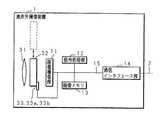
以下、本発明の実施の形態について、図面を参照しながら詳細に説明する。図1は、本発明の実施の形態に係る遠赤外撮像装置1の構成を示すブロック図である。なお、本実施の形態に係る遠赤外撮像装置1は、波長が7〜14マイクロメートルの赤外光を用いた撮像装置である。 Hereinafter, embodiments of the present invention will be described in detail with reference to the drawings. FIG. 1 is a block diagram showing a configuration of a far-
図1において、画像撮像部11は、光学信号を電気信号に変換する撮像素子をマトリックス状に備えている。遠赤外用の撮像素子としては、マイクロマシニング(micromachining)技術を用いた酸化バナジウムのボロメータ型、BSTO(Barium-Titanium Oxide)の焦電型等の赤外線センサを用いる。 In FIG. 1, an
画像撮像部11は、車両の周囲の赤外光像を輝度信号として読み取り、読み取った輝度信号を、LSI基板である信号処理部12へ送信する。図2は、本発明の実施の形態に係る遠赤外撮像装置1の信号処理部12の構成を示すブロック図である。信号処理部12は、LSI16が動作を制御するA/D変換部121、NUC(Non-Uniformity Correction)処理部122、BPR(Bad-Pixel Replacement)処理部123、及びフラッシュメモリ等の不揮発性メモリ、SRAM等の一時記憶用メモリであるRAM125で構成されている。 The
信号処理部12は、画像撮像部11から受信した輝度信号をA/D変換部121でデジタル信号に変換し、NUC(Non-Uniformity Correction)処理部122で撮像素子ごとに出力された輝度信号を補正する。 The
NUC処理部122では、キャリブレーションによる補正係数として、撮像素子ごとに所定の温度に対する出力値を補正するオフセット補正値、及び撮像素子ごとに所定の温度変化率に対する出力値の差異を補正するゲイン補正値を算出して、輝度信号を補正する。例えばi行j列のマトリックス状に配列された撮像素子ごとの出力輝度値をVijとした場合、NUC処理部では(数1)に示す演算を行うことにより撮像素子ごとの輝度値をV’ijへ補正する。In the

(数1)において、Gijはゲイン補正値を、Oijはオフセット補正値を示しており、例えば黒体炉、シャッター等の温度分布が均一である物体を撮像した場合の撮像素子ごとの出力輝度値に基づいて算出した値である。In (Expression 1), Gij represents a gain correction value, and Oij represents an offset correction value. For example, an output for each image sensor when an object having a uniform temperature distribution such as a black body furnace or a shutter is imaged. This is a value calculated based on the luminance value.
本実施の形態では、表面の温度分布が略均一である板状のシャッター32を対物レンズ31と画像撮像部11との間に開閉することが可能に設けてあり、シャッター32が閉じられた状態で撮像した場合の撮像素子ごとの出力輝度値に基づいて、オフセット補正値を随時補正する。なお、図1では、機械式のプレーンシャッターを例に挙げてしているが、表面の温度分布が均一であれば、どのような構成のシャッターであっても良い。 In the present embodiment, a plate-
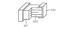
オフセット補正値により、撮像対象物の温度が同一である場合には同一の輝度値を出力するよう補正するためには、シャッター32の表面の絶対温度を取得し、対応する輝度値を出力するようオフセット補正値を算出する必要がある。そこで、本実施の形態では、シャッター32の表面温度を検出する手段として、シャッター32の表面に接触して表面温度を計測する接触型温度センサ33、例えばサーミスタ、半導体温度センサ、熱電対等をシャッター32の画像撮像部11側の表面に取り付けてある。図3は、本発明の実施の形態に係る遠赤外撮像装置1の接触型温度センサ33として用いるサーミスタ33aの構成を示す模式図である。 In order to perform correction so that the same luminance value is output when the temperature of the imaging object is the same by the offset correction value, the absolute temperature of the surface of the
本実施の形態に係るサーミスタ33aは、いわゆるチップ型と呼ばれる略直方体形状を有しており、セラミック半導体331を積層して、内部に内部電極332を各階層間に挟持してある。内部電極は、図示しない中間電極を介して外部電極333と接続されており、外部電圧を印加することで電流が流れる。シャッター32の表面には、外部電極333の両側面を半田付けし、シャッター32の温度変化に応じてセラミック半導体331の抵抗値が変動する。該抵抗値の変動に応じて、内部を流れる電流値が変動する。したがって、電流値の変動を追従することにより、精度の高い温度計測手段として機能させることが可能となる。サーミスタ33aで検出した温度に応じた電流値は、温度信号として信号処理部12へ送信される。 The thermistor 33a according to the present embodiment has a substantially rectangular parallelepiped shape called a so-called chip type, in which a
またサーミスタ33aの代わりに半導体温度センサ33bを用いても良い。半導体温度センサ33bは、内部にトランジスタを備えており、ベース−エミッタ間の電圧Vbeが周囲の温度に対して略直線的に変化する特性を利用したものである。すなわち、温度と半導体温度センサ33bの出力電圧とは一次比例の関係にあり、外付けの抵抗を必要とすることなく半導体温度センサ33bから直接出力することができる。これにより、より取り付けが容易で、シャッター32の表面温度をより正確に検出することが可能となる。 A semiconductor temperature sensor 33b may be used instead of the thermistor 33a. The semiconductor temperature sensor 33b includes a transistor inside, and utilizes a characteristic that the base-emitter voltage Vbe changes substantially linearly with respect to the ambient temperature. That is, the temperature and the output voltage of the semiconductor temperature sensor 33b are in a linear relationship, and can be directly output from the semiconductor temperature sensor 33b without requiring an external resistor. As a result, attachment is easier and the surface temperature of the
信号処理部12のLSI16は、シャッター32が閉じられた状態での表面温度及び出力輝度値を取得し、取得した表面温度及び撮像素子ごとの出力輝度値に基づいてオフセット補正値及びゲイン補正値を算出する。算出したオフセット補正値及びゲイン補正値は、RAM125に記憶しておき、NUC処理部122は、記憶してあるオフセット補正値及びゲイン補正値に基づいて撮像素子ごとに出力された輝度信号を補正する。 The
なお、撮像素子には所定の割合で欠陥が生じている撮像素子が含まれる。したがって、LSI16は、BPR(Bad-Pixel Replacement)処理部123にて、欠陥が生じている撮像素子の出力値を、周囲の撮像素子の出力値を代表する値、例えば欠陥が生じている撮像素子の出力値を除外した周囲の撮像素子の出力値の平均値へ補正する。撮像素子ごとに補正された出力値は、画像データとして画像メモリ13へ記憶される。 The image sensor includes an image sensor in which defects are generated at a predetermined rate. Therefore, the
通信インタフェース部14は、LSI基板であり、通信ケーブル等の通信線2を介して外部の装置から受信した指令に従って、画像メモリ13に記憶された画像データの外部の装置への送出、撮像した画像の解像度による転送レートの変換、画像データを送出するためのデータのフォーマット変換等を行う。 The
以下、信号処理部12のLSI16でのキャリブレーション処理について説明する。図4は、本発明の実施の形態に係る遠赤外撮像装置1の信号処理部12のLSI16のキャリブレーション処理の手順を示すフローチャートである。 Hereinafter, calibration processing in the
遠赤外撮像装置1の画像撮像部11は、温度分布が均一であるシャッター32を撮像し、撮像素子ごとの出力値が信号処理部12へ送信される。信号処理部12のLSI16は、画像撮像部11から撮像素子ごとの輝度信号を受信し(ステップS401)、デジタル信号Vijへ変換する(ステップS402)。また、接触型温度センサ33からシャッター32の表面温度を取得する(ステップS403)。The
LSI16は、所定の撮像素子、例えば接触型温度センサ33の取り付け位置近傍の撮像素子のデジタル化された輝度値Vijを基準輝度値として、全ての輝度値が基準輝度値となるようゲイン補正値及びオフセット補正値を撮像素子ごとに算出し(ステップS404)、シャッター32の表面温度と対応付けてRAM125に記憶する(ステップS405)。すなわち、キャリブレーション実行時のシャッター32の表面温度を基準温度とし、基準温度でのゲイン補正値及びオフセット補正値を算出することになる。The
実際の撮像時には、LSI16は、RAM125に記憶されているゲイン補正値及びオフセット補正値を用いて、画像撮像部11で撮像された輝度信号は補正される。しかし、RAM125に記憶されているのは基準温度に基づいて算出されたゲイン補正値及びオフセット補正値であり、基準温度と撮像時のシャッター32の表面温度とが一般に相違することから、RAM125に記憶されているゲイン補正値及びオフセット補正値をそのまま使用することはできない。 At the time of actual imaging, the
ここで、オフセット補正値は、絶対温度であるシャッター32のキャリブレーション実行時の表面温度に対応して算出されており、撮像時のシャッター32の表面温度との差に応じて補正することにより、絶対温度に対する出力輝度値を正しく出力するよう補正することができる。一方、温度変化率に対する出力値を補正するゲイン補正値は、シャッター32の表面温度の変化に対して大きく変動することがないので、オフセット補正値のように随時キャリブレーションを実行して補正する必要性に乏しい。 Here, the offset correction value is calculated corresponding to the surface temperature at the time of calibration of the
そこで、本実施の形態に係る遠赤外撮像装置1の撮像に際し、シャッター32を閉じて簡便なキャリブレーションを実行することにより、オフセット補正値を推定して補正する。図5は、本発明の実施の形態に係る遠赤外撮像装置1の信号処理部12のLSI16のオフセット補正値の補正処理の手順を示すフローチャートである。Therefore, when the far-
遠赤外撮像装置1は、撮像素子ごとの出力値を信号処理部12へ送信する。信号処理部12のLSI16は、画像撮像部11からの撮像素子ごとの輝度信号を受信し(ステップS501)、デジタル信号Vijへ変換する(ステップS502)。The far-
LSI16は、RAM125に記憶してあるゲイン補正値及びオフセット補正値を撮像素子ごとに読み出す(ステップS503)。またLSI16は、接触型温度センサ33からシャッター32の表面温度を取得し(ステップS504)、取得した表面温度に基づいて、読み出した撮像素子ごとのオフセット補正値を補正する(ステップS505)。 The
取得した表面温度に対応したオフセット補正値は、基準温度に対応したオフセット補正値を複数記憶しておき、取得した表面温度に応じて線形補間することにより推定する。オフセット補正値の補正方法は、特にこれに限定されるものではなく、例えば複数の温度に対するキャリブレーション結果に基づいて線形関数を事前に求めておき、取得した表面温度を変数として算出してもよい。The offset correction value corresponding to the acquired surface temperature is estimated by storing a plurality of offset correction values corresponding to the reference temperature and performing linear interpolation according to the acquired surface temperature. Thecorrection method of the offset correction value is not particularly limited to this, and for example, a linear function may be obtained in advance based on calibration results for a plurality of temperatures, and the obtained surface temperature may be calculated as a variable. .
LSI16は、抽出したゲイン補正値及び算出したオフセット補正値を用いて撮像素子ごとの輝度値Vijを出力輝度値V’ijへ補正し(ステップS506)、画像メモリ13へ記憶する(ステップS507)。通信インタフェース部14は、外部の装置から送出される指令に従って、画像メモリ13に記憶された画像データを外部の装置へ送出するためのパケットデータを生成して、外部の装置へ送出する。The
本実施の形態にかかる遠赤外撮像装置1からの出力値は、上述した処理を経ることにより、絶対温度に対応した輝度値となっている。すなわち、出力された輝度値に基づいて、撮像した対象物の表面温度の絶対値を容易に推定することが可能となる。したがって、本実施の形態に係る遠赤外撮像装置1を、例えば障害物検出システムに適用した場合、検出された障害物の表面温度の絶対値に基づいて、人間であるか否か、原動機が存在するか否か等を判断することができ、障害物の種類をより正確に特定することが可能となる。 The output value from the far-
以上のように本実施の形態によれば、絶対温度に対応してオフセット補正値を算出することができ、輝度値に基づいて撮像対象物の絶対温度を容易に推定することができる。例えば所定の時間間隔、撮像開始前等にシャッターを閉じてキャリブレーションを実行することにより、オフセット補正値を絶対温度に対応付けて補正することができ、長期に渡り出力値を絶対温度に対応付けて出力することが可能となる。 As described above, according to the present embodiment, the offset correction value can be calculated corresponding to the absolute temperature, and the absolute temperature of the imaging target can be easily estimated based on the luminance value. For example, by performing calibration with the shutter closed at a predetermined time interval or before imaging starts, the offset correction value can be corrected in association with the absolute temperature, and the output value can be correlated with the absolute temperature over a long period of time. Can be output.
なお、上述した実施の形態では、遠赤外撮像装置1の信号処理部12のLSI16が上述した処理を行っているが、後続の処理、例えば障害物検出処理、衝突判定処理等を行う演算装置のMPU、CPU等が実行しても良い。 In the above-described embodiment, the
また、本実施の形態では、遠赤外撮像装置1の撮像開始前にシャッター32を閉じてキャリブレーションを実行しているが、キャリブレーションを実行するタイミングはこれに限定されるものではなく、例えば一定時間ごとにキャリブレーションを実行して、オフセット補正値を補正しても良い。 In the present embodiment, the calibration is executed by closing the
1 遠赤外撮像装置
2 通信線
11 画像撮像部
12 信号処理部
13 画像メモリ
14 通信インタフェース部
15 内部バス
16 LSI
33 接触型温度センサ
33a サーミスタ
33b 半導体温度センサ
121 A/D変換部
122 NUC処理部
123 BPR処理部
125 RAMDESCRIPTION OF
33 Contact-type temperature sensor 33a Thermistor 33b Semiconductor temperature sensor 121 A /
Claims (3)
Translated fromJapanese該撮像素子ごとに所定の温度に対する出力値を補正するオフセット補正値を算出するオフセット補正値算出手段と、
前記撮像素子ごとに所定の温度変化率に対する出力値の差異を補正するゲイン補正値を算出するゲイン補正値算出手段と
を備え、
前記オフセット補正値算出手段及びゲイン補正値算出手段の夫々が算出したオフセット補正値及びゲイン補正値により撮像素子ごとに出力値を補正して撮像データを取得する遠赤外撮像装置において、
表面温度が略均一であり、前記撮像素子へ入光させる開口を開閉するシャッターと、
該シャッターの表面温度を計測する温度計測手段と、
前記撮像素子ごとに複数の温度夫々に対して、前記オフセット補正値算出手段が算出したオフセット補正値を予め記憶する記憶手段と
を備え、
前記オフセット補正値算出手段は、前記記憶手段が記憶した複数の温度夫々に対するオフセット補正値を照会して、前記温度計測手段が前記シャッターを閉じた状態で計測した前記シャッターの表面温度に対する撮像素子ごとのオフセット補正値を補正するようにしてあること
を特徴とする遠赤外撮像装置。A plurality of imaging devices arranged in a matrix;
Offset correction value calculating means for calculating an offset correction value for correcting an output value for a predetermined temperature for each image sensor;
Gain correction value calculating means for calculating a gain correction value for correcting a difference in output value with respect to a predetermined temperature change rate for each of the image sensors;
In the far-infrared imaging device that acquires the imaging data by correcting the output value for each imaging elementby the offset correction value and the gain correction valuecalculated by each of the offset correction value calculation unit and the gain correction value calculation unit ,
Surface temperature is substantially uniform, and a shutter for opening and closing an opening for incident light tothe imaging element;
Temperature measuring means for measuring the surface temperature of the shutter;
Storage means for storing in advance the offset correction value calculated by the offset correction value calculation means for each of a plurality of temperatures for each image sensor ;
The offset correction value calculating means, the image pickupagainstthe storage means to query the offset correction value for each of the plurality of temperature husband stored, the surface temperature ofthesaidshutter temperature measuring means hasa total measuredin a state of closing said shutter A far-infrared imaging device, wherein an offset correction value for each element iscorrected .
前記撮像素子ごとに複数の温度夫々に対して算出したオフセット補正値を予め記憶し、
表面温度が略均一であるシャッターを閉じた状態で該シャッターの表面温度を取得し、
記憶した複数の温度夫々に対するオフセット補正値を照会して、取得した表面温度に対する撮像素子ごとのオフセット補正値を補正すること
を特徴とする出力値補正方法。An offset correction value for correcting an output value for a predetermined temperature is calculated for each of a plurality of image sensors arranged in a matrix on the far-infrared imaging device, and a difference in output value with respect to a predetermined temperature change rate is calculated for each of the image sensors. In an output value correction method for calculating a gain correction value to be corrected, and correcting an output value for each image sensor bythe calculated offset correction value and gain correction value.
An offset correction value calculated for each of a plurality of temperatures for each image sensor is stored in advance,
Get the surface temperatureof the shutter in a state where the surface temperature is closing the shutter is substantially uniform,
An output value correction methodcomprising: querying an offset correction value for each of a plurality of stored temperatures andcorrecting the offset correction value for each imaging device withrespectto the acquiredsurface temperature .
Priority Applications (1)
| Application Number | Priority Date | Filing Date | Title |
|---|---|---|---|
| JP2006017837AJP4742883B2 (en) | 2006-01-26 | 2006-01-26 | Far-infrared imaging device and output value correction method |
Applications Claiming Priority (1)
| Application Number | Priority Date | Filing Date | Title |
|---|---|---|---|
| JP2006017837AJP4742883B2 (en) | 2006-01-26 | 2006-01-26 | Far-infrared imaging device and output value correction method |
Publications (2)
| Publication Number | Publication Date |
|---|---|
| JP2007201807A JP2007201807A (en) | 2007-08-09 |
| JP4742883B2true JP4742883B2 (en) | 2011-08-10 |
Family
ID=38455945
Family Applications (1)
| Application Number | Title | Priority Date | Filing Date |
|---|---|---|---|
| JP2006017837AExpired - Fee RelatedJP4742883B2 (en) | 2006-01-26 | 2006-01-26 | Far-infrared imaging device and output value correction method |
Country Status (1)
| Country | Link |
|---|---|
| JP (1) | JP4742883B2 (en) |
Families Citing this family (7)
| Publication number | Priority date | Publication date | Assignee | Title |
|---|---|---|---|---|
| JP2009246731A (en)* | 2008-03-31 | 2009-10-22 | Chino Corp | Pixel correcting device |
| JP6540519B2 (en)* | 2016-01-12 | 2019-07-10 | 三菱電機株式会社 | Infrared imaging device |
| JP6866655B2 (en) | 2017-01-31 | 2021-04-28 | 株式会社Jvcケンウッド | Thermal image processing device, infrared imaging device, thermal image processing method, and thermal image processing program |
| KR101824607B1 (en)* | 2017-08-11 | 2018-03-14 | 엘아이지넥스원 주식회사 | Method for compensating infra-red image |
| KR101824604B1 (en)* | 2017-08-17 | 2018-02-01 | 엘아이지넥스원 주식회사 | Apparatus for compensating infra-red image and system using thereof |
| KR102657953B1 (en)* | 2020-12-08 | 2024-04-18 | (주)유우일렉트로닉스 | Apparatus, method and computer readable medium for correcting temperature of object using shutter |
| JP2023074749A (en) | 2021-11-18 | 2023-05-30 | 株式会社Jvcケンウッド | Control system and control method |
Family Cites Families (1)
| Publication number | Priority date | Publication date | Assignee | Title |
|---|---|---|---|---|
| EP1160550A4 (en)* | 1999-01-14 | 2008-01-30 | Matsushita Electric Industrial Co Ltd | INFRARED IMAGING APPARATUS, A VEHICLE EQUIPPED THEREWITH, AND DEVICE FOR ADJUSTING AN INFRARED IMAGE |
- 2006
- 2006-01-26JPJP2006017837Apatent/JP4742883B2/ennot_activeExpired - Fee Related
Also Published As
| Publication number | Publication date |
|---|---|
| JP2007201807A (en) | 2007-08-09 |
Similar Documents
| Publication | Publication Date | Title |
|---|---|---|
| JP4742883B2 (en) | Far-infrared imaging device and output value correction method | |
| CN110974186B (en) | Temperature monitoring system and method for determining temperature change of target area | |
| EP1732314B1 (en) | Infrared camera with humidity sensor | |
| CN109916517B (en) | Thermal image processing system and method | |
| JP6540519B2 (en) | Infrared imaging device | |
| CN113678165B (en) | Device for hot spot sensing | |
| US9383540B1 (en) | System and method for controlling the focus of a lens | |
| JP4016022B2 (en) | Infrared imaging device and vehicle equipped with the same | |
| JP4910529B2 (en) | Obstacle detection system and obstacle detection method | |
| US10788644B2 (en) | Lens device, imaging device, and focus shift correction method of lens device | |
| CN111623885A (en) | Infrared temperature measuring device and infrared temperature measuring method | |
| US20180376088A1 (en) | Techniques for correcting fixed pattern noise in shutterless fir cameras | |
| JP4807152B2 (en) | Obstacle detection system and obstacle detection method | |
| KR102312521B1 (en) | Externally mounted temperature calibration device for thermal imaging cameras and temperature measurement system using it | |
| JP6112351B2 (en) | Inclination angle correction apparatus, inclination angle correction program, inclination angle correction method, and imaging apparatus | |
| US20220061675A1 (en) | Forehead temperature measurement system with high accuracy | |
| US10362303B2 (en) | Sensor-assisted autofocus calibration | |
| JP2007325120A (en) | Far infrared imaging system and far infrared imaging method | |
| JP2007174113A (en) | Obstacle detection system and obstacle detection method | |
| JP4816308B2 (en) | Far infrared imaging system and far infrared imaging method | |
| JP2009246731A (en) | Pixel correcting device | |
| JP4835332B2 (en) | Far infrared imaging system and far infrared imaging method | |
| JP4222364B2 (en) | Infrared light imaging apparatus and infrared light imaging method | |
| JP2009150842A (en) | Temperature measuring device and vehicle | |
| JP7638409B1 (en) | Infrared imaging device and output value correction method for infrared imaging device |
Legal Events
| Date | Code | Title | Description |
|---|---|---|---|
| A621 | Written request for application examination | Free format text:JAPANESE INTERMEDIATE CODE: A621 Effective date:20081015 | |
| A977 | Report on retrieval | Free format text:JAPANESE INTERMEDIATE CODE: A971007 Effective date:20100727 | |
| A131 | Notification of reasons for refusal | Free format text:JAPANESE INTERMEDIATE CODE: A131 Effective date:20100803 | |
| A521 | Request for written amendment filed | Free format text:JAPANESE INTERMEDIATE CODE: A523 Effective date:20100930 | |
| A01 | Written decision to grant a patent or to grant a registration (utility model) | Free format text:JAPANESE INTERMEDIATE CODE: A01 Effective date:20110412 | |
| A61 | First payment of annual fees (during grant procedure) | Free format text:JAPANESE INTERMEDIATE CODE: A61 Effective date:20110425 | |
| FPAY | Renewal fee payment (event date is renewal date of database) | Free format text:PAYMENT UNTIL: 20140520 Year of fee payment:3 | |
| R150 | Certificate of patent or registration of utility model | Free format text:JAPANESE INTERMEDIATE CODE: R150 | |
| R250 | Receipt of annual fees | Free format text:JAPANESE INTERMEDIATE CODE: R250 | |
| R250 | Receipt of annual fees | Free format text:JAPANESE INTERMEDIATE CODE: R250 | |
| LAPS | Cancellation because of no payment of annual fees |