JP4741026B2 - Integrated touch screen - Google Patents
Integrated touch screenDownload PDFInfo
- Publication number
- JP4741026B2 JP4741026B2JP2010036614AJP2010036614AJP4741026B2JP 4741026 B2JP4741026 B2JP 4741026B2JP 2010036614 AJP2010036614 AJP 2010036614AJP 2010036614 AJP2010036614 AJP 2010036614AJP 4741026 B2JP4741026 B2JP 4741026B2
- Authority
- JP
- Japan
- Prior art keywords
- pixel
- display
- touch
- region
- display pixels
- Prior art date
- Legal status (The legal status is an assumption and is not a legal conclusion. Google has not performed a legal analysis and makes no representation as to the accuracy of the status listed.)
- Expired - Fee Related
Links
Images


Classifications
- G—PHYSICS
- G06—COMPUTING OR CALCULATING; COUNTING
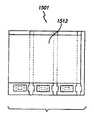
- G06F—ELECTRIC DIGITAL DATA PROCESSING
- G06F3/00—Input arrangements for transferring data to be processed into a form capable of being handled by the computer; Output arrangements for transferring data from processing unit to output unit, e.g. interface arrangements
- G06F3/01—Input arrangements or combined input and output arrangements for interaction between user and computer
- G06F3/03—Arrangements for converting the position or the displacement of a member into a coded form
- G06F3/041—Digitisers, e.g. for touch screens or touch pads, characterised by the transducing means
- G06F3/0412—Digitisers structurally integrated in a display
- G—PHYSICS
- G02—OPTICS
- G02F—OPTICAL DEVICES OR ARRANGEMENTS FOR THE CONTROL OF LIGHT BY MODIFICATION OF THE OPTICAL PROPERTIES OF THE MEDIA OF THE ELEMENTS INVOLVED THEREIN; NON-LINEAR OPTICS; FREQUENCY-CHANGING OF LIGHT; OPTICAL LOGIC ELEMENTS; OPTICAL ANALOGUE/DIGITAL CONVERTERS
- G02F1/00—Devices or arrangements for the control of the intensity, colour, phase, polarisation or direction of light arriving from an independent light source, e.g. switching, gating or modulating; Non-linear optics
- G02F1/01—Devices or arrangements for the control of the intensity, colour, phase, polarisation or direction of light arriving from an independent light source, e.g. switching, gating or modulating; Non-linear optics for the control of the intensity, phase, polarisation or colour
- G02F1/13—Devices or arrangements for the control of the intensity, colour, phase, polarisation or direction of light arriving from an independent light source, e.g. switching, gating or modulating; Non-linear optics for the control of the intensity, phase, polarisation or colour based on liquid crystals, e.g. single liquid crystal display cells
- G02F1/133—Constructional arrangements; Operation of liquid crystal cells; Circuit arrangements
- G02F1/1333—Constructional arrangements; Manufacturing methods
- G02F1/13338—Input devices, e.g. touch panels
- G—PHYSICS
- G06—COMPUTING OR CALCULATING; COUNTING
- G06F—ELECTRIC DIGITAL DATA PROCESSING
- G06F3/00—Input arrangements for transferring data to be processed into a form capable of being handled by the computer; Output arrangements for transferring data from processing unit to output unit, e.g. interface arrangements
- G06F3/01—Input arrangements or combined input and output arrangements for interaction between user and computer
- G06F3/03—Arrangements for converting the position or the displacement of a member into a coded form
- G06F3/041—Digitisers, e.g. for touch screens or touch pads, characterised by the transducing means
- G06F3/0416—Control or interface arrangements specially adapted for digitisers
- G06F3/04166—Details of scanning methods, e.g. sampling time, grouping of sub areas or time sharing with display driving
- G—PHYSICS
- G06—COMPUTING OR CALCULATING; COUNTING
- G06F—ELECTRIC DIGITAL DATA PROCESSING
- G06F3/00—Input arrangements for transferring data to be processed into a form capable of being handled by the computer; Output arrangements for transferring data from processing unit to output unit, e.g. interface arrangements
- G06F3/01—Input arrangements or combined input and output arrangements for interaction between user and computer
- G06F3/03—Arrangements for converting the position or the displacement of a member into a coded form
- G06F3/041—Digitisers, e.g. for touch screens or touch pads, characterised by the transducing means
- G06F3/0416—Control or interface arrangements specially adapted for digitisers
- G06F3/0418—Control or interface arrangements specially adapted for digitisers for error correction or compensation, e.g. based on parallax, calibration or alignment
- G06F3/04184—Synchronisation with the driving of the display or the backlighting unit to avoid interferences generated internally
- G—PHYSICS
- G06—COMPUTING OR CALCULATING; COUNTING
- G06F—ELECTRIC DIGITAL DATA PROCESSING
- G06F3/00—Input arrangements for transferring data to be processed into a form capable of being handled by the computer; Output arrangements for transferring data from processing unit to output unit, e.g. interface arrangements
- G06F3/01—Input arrangements or combined input and output arrangements for interaction between user and computer
- G06F3/03—Arrangements for converting the position or the displacement of a member into a coded form
- G06F3/041—Digitisers, e.g. for touch screens or touch pads, characterised by the transducing means
- G06F3/044—Digitisers, e.g. for touch screens or touch pads, characterised by the transducing means by capacitive means
- G06F3/0443—Digitisers, e.g. for touch screens or touch pads, characterised by the transducing means by capacitive means using a single layer of sensing electrodes
- G—PHYSICS
- G06—COMPUTING OR CALCULATING; COUNTING
- G06F—ELECTRIC DIGITAL DATA PROCESSING
- G06F3/00—Input arrangements for transferring data to be processed into a form capable of being handled by the computer; Output arrangements for transferring data from processing unit to output unit, e.g. interface arrangements
- G06F3/01—Input arrangements or combined input and output arrangements for interaction between user and computer
- G06F3/03—Arrangements for converting the position or the displacement of a member into a coded form
- G06F3/041—Digitisers, e.g. for touch screens or touch pads, characterised by the transducing means
- G06F3/044—Digitisers, e.g. for touch screens or touch pads, characterised by the transducing means by capacitive means
- G06F3/0446—Digitisers, e.g. for touch screens or touch pads, characterised by the transducing means by capacitive means using a grid-like structure of electrodes in at least two directions, e.g. using row and column electrodes
- G—PHYSICS
- G06—COMPUTING OR CALCULATING; COUNTING
- G06F—ELECTRIC DIGITAL DATA PROCESSING
- G06F2203/00—Indexing scheme relating to G06F3/00 - G06F3/048
- G06F2203/041—Indexing scheme relating to G06F3/041 - G06F3/045
- G06F2203/04103—Manufacturing, i.e. details related to manufacturing processes specially suited for touch sensitive devices
Landscapes
- Engineering & Computer Science (AREA)
- Theoretical Computer Science (AREA)
- General Engineering & Computer Science (AREA)
- Physics & Mathematics (AREA)
- General Physics & Mathematics (AREA)
- Human Computer Interaction (AREA)
- Nonlinear Science (AREA)
- Optics & Photonics (AREA)
- Crystallography & Structural Chemistry (AREA)
- Chemical & Material Sciences (AREA)
- Mathematical Physics (AREA)
- Liquid Crystal (AREA)
- Devices For Indicating Variable Information By Combining Individual Elements (AREA)
- Position Input By Displaying (AREA)
- Control Of Indicators Other Than Cathode Ray Tubes (AREA)
- Liquid Crystal Display Device Control (AREA)
Abstract
Description
Translated fromJapanese(関連出願の相互参照)
本出願は、2009年2月2日に出願の米国特許仮出願第61/149,340号及び2009年2月27日に出願の米国特許仮出願番号第61/156,463号の利益を主張するものであり、当該特許の内容は、全ての目的において引用により全体が本明細書に組み込まれる。(Cross-reference of related applications)
This application claims the benefit of US Provisional Application No. 61 / 149,340, filed February 2, 2009, and US Provisional Application No. 61 / 156,463, filed February 27, 2009. The contents of which are incorporated herein by reference in their entirety for all purposes.
本出願は、一般に、表示画素スタックアップを含むディスプレイに関し、更に詳細には、ディスプレイの表示画素スタックアップに一体化されたタッチ感知回路に関する。 The present application relates generally to displays that include a display pixel stackup, and more particularly to touch sensing circuitry integrated into the display pixel stackup of the display.
ボタン又はキー、マウス、トラックボール、ジョイスティック、タッチセンサパネル、タッチスクリーン、及び同様のものなど、コンピュータシステムにおいて操作を行うために多くの形式の入力デバイスが現在利用可能である。特に、タッチスクリーンは、操作のし易さ及び汎用性、並びに価格の低下に起因してますます人気が高まっている。タッチスクリーンは、タッチ感応面を有する透明パネルとすることができるタッチセンサパネルと、タッチ感応表面がディスプレイデバイスの可視区域の少なくとも一部を覆うことができるようにパネルの後方に部分的又は完全に位置決めすることができる、液晶ディスプレイ(LCD)などのディスプレイデバイスとを含むことができる。タッチスクリーンは、ディスプレイデバイスにより表示されるユーザインタフェース(UI)によって多くの場合指図される位置において、ユーザが、指、スタイラス又は他の物体を使用してタッチセンサパネルにタッチすることで種々の機能を行うことを可能にすることができる。一般に、タッチスクリーンは、タッチセンサパネル上のタッチ及びタッチの位置を認識することができ、次いで、コンピュータシステムは、タッチ時に表示されているディスプレイに従ってタッチを解釈し、その後、タッチに基づいて1つ又はそれ以上のアクションを行うことができる。一部のタッチ感知システムの場合、ディスプレイ上の物理的タッチは、タッチを検出するのに必要ではない。例えば、一部の容量式タッチ感知システムおいては、タッチを検出するのに使用されるフリンジフィールドは、ディスプレイ表面を超えて延在することができ、表面近くに接近する物体を表面に実際に接触せずに表面近傍で検出することができる。 Many types of input devices are currently available for performing operations in computer systems, such as buttons or keys, mice, trackballs, joysticks, touch sensor panels, touch screens, and the like. In particular, touch screens are becoming increasingly popular due to ease of operation and versatility, and price reduction. The touch screen is partially or completely behind the touch sensor panel, which can be a transparent panel having a touch-sensitive surface, and the panel so that the touch-sensitive surface can cover at least part of the visible area of the display device. And a display device such as a liquid crystal display (LCD) that can be positioned. Touch screens have various functions by allowing a user to touch a touch sensor panel using a finger, stylus or other object at a location often directed by a user interface (UI) displayed by a display device. Can be made possible. In general, the touch screen can recognize the touch and the position of the touch on the touch sensor panel, and then the computer system interprets the touch according to the display that is displayed at the time of touch, and then one based on the touch. Or more actions can be taken. For some touch sensitive systems, a physical touch on the display is not necessary to detect a touch. For example, in some capacitive touch sensing systems, the fringe field used to detect touches can extend beyond the display surface, and objects approaching the surface are actually on the surface. Detection is possible in the vicinity of the surface without contact.
容量性タッチセンサパネルは、実質的に透明の基板上で水平方向及び垂直方向に横列及び縦列状態で配設されることが多い、酸化インジウムスズ(ITO)などの実質的に透明な導電性材料の駆動線及び感知線のマトリクスから形成することができる。上述のようにタッチスクリーンを形成するために容量性タッチセンサパネルをディスプレイ上に重ね合わせることができることは、1つには、実質的に透過性であることに起因する。しかしながら、タッチセンサパネルとディスプレイの重ね合わせは、重量及び厚さの増加、タッチセンサパネルを駆動するのに必要とされる電力の増加、及びディスプレイ輝度の減少などの欠点を有することがある。 Capacitive touch sensor panels are substantially transparent conductive materials such as indium tin oxide (ITO) that are often arranged in rows and columns horizontally and vertically on a substantially transparent substrate. It can be formed from a matrix of drive lines and sense lines. The ability to overlay a capacitive touch sensor panel on a display to form a touch screen as described above is due in part to being substantially transmissive. However, the overlay of the touch sensor panel and the display may have drawbacks such as increased weight and thickness, increased power required to drive the touch sensor panel, and decreased display brightness.
本出願は、LCDディスプレイなどのディスプレイの表示画素スタックアップ(すなわち、表示画素を形成するスタック材料層)に一体化されたタッチ感知回路に関する。表示画素スタックアップ内の回路素子を併せてグループ化し、ディスプレイ上又はその近傍のタッチを感知するタッチ感知回路を形成することができる。タッチ感知回路は、例えば、駆動線及び感知線などのタッチ信号線、接地領域、及び他の回路を含むことができる。一体型タッチスクリーンは、ディスプレイ上で画像を生成するディスプレイシステムの回路として動作するように設計された表示回路の一部を形成することができ、更にまた、ディスプレイ上又はその近傍で1つ又はそれ以上のタッチを感知するタッチ感知システムのタッチ感知回路の一部を形成することもできる、多機能回路素子を含むことができる。多機能回路素子は、例えば、LCDの表示画素のキャパシタとすることができ、ディスプレイシステムの表示回路の蓄積キャパシタ/電極、共通電極、導電線/導電路、その他として動作するように構成することができ、更に、タッチ感知回路の回路素子として動作するよう構成することもできる。このようにすると、例えば、幾つかの実施形態においては、一体化されたタッチ感知能力を有するディスプレイを、より少数の部品及び/又は処理段階を用いて製造することができ、ディスプレイ自体を薄肉化、高輝度化、及び低所要電力化することができる。 The present application relates to a touch sensing circuit integrated into a display pixel stack-up of a display such as an LCD display (ie, a stack material layer that forms a display pixel). The circuit elements in the display pixel stackup can be grouped together to form a touch sensing circuit that senses a touch on or near the display. The touch sensing circuit may include, for example, touch signal lines such as driving lines and sensing lines, a ground region, and other circuits. An integrated touch screen can form part of a display circuit designed to operate as a display system circuit that generates an image on the display, and also one or more on or near the display. Multi-function circuit elements that can also form part of the touch sensing circuit of the touch sensing system that senses the touch described above can be included. The multifunctional circuit element can be, for example, a capacitor of a display pixel of an LCD, and can be configured to operate as a storage capacitor / electrode, a common electrode, a conductive line / conductive path, etc. Furthermore, it can be configured to operate as a circuit element of the touch sensing circuit. In this way, for example, in some embodiments, a display with integrated touch sensing capability can be manufactured with fewer components and / or processing steps, and the display itself is thinned. , High luminance, and low power requirements.
例示的な実施形態の以下の説明において、本明細書の一部を形成し、本開示の実施形態を実施することができる特定の実施形態を例証として示された添付図面を参照する。他の実施形態を用いることができ、本開示の実施形態の範囲から逸脱することなく構造的変更を行うことができる点を理解されたい。 In the following description of exemplary embodiments, reference is made to the accompanying drawings that form a part hereof, and in which are shown by way of illustration specific embodiments in which embodiments of the disclosure may be practiced. It should be understood that other embodiments may be used and structural changes may be made without departing from the scope of the embodiments of the present disclosure.
以下の説明は、LCDディスプレイなどのディスプレイの表示画素スタックアップ(すなわち、表示画素を形成するスタック材料層)にタッチ感知回路を一体化することができる実施例を含む。本明細書の実施形態はLCDディスプレイに関して説明するが、一般に、電気的に画像形成可能材料を含む、あらゆる電気的に画像形成可能な層など、LCDディスプレイではなく代替のディスプレイを利用することができる点を理解されたい。電気的に画像形成可能な材料は、発光又は光変調することができる。発光材料は、本質的に無機又は有機とすることができる。好適な材料としては、有機発光ダイオード(OLED)又は高分子発光ダイオード(PLED)を挙げることができる。光変調材料は、反射式又は透過式とすることができる。光変調材料としては、限定ではないが、電気化学材料、Gyricon粒子などの電気泳動材料、エレクトロクロミック材料、又は液晶材料を挙げることができる。液晶材料は、限定ではないが、ツイステッドネマチック(TN)液晶、スーパツイステッドネマティック(STN)液晶、強誘電性液晶、磁気液晶、又はキラルネマチック液晶とすることができる。他の好適な材料として、サーモクロミック材料、荷電粒子、及び磁性粒子を挙げることができる。タッチ感知回路は、例えば、駆動線及び感知線などのタッチ信号線、接地領域、及び他の回路を含むことができる。表示画素スタックアップは通常、導電性材料(例えば、金属、実質的に透明導体)、半導電性材料(例えば、多結晶シリコン(poly−Si))及び誘電材料(例えば、Si02、有機物質、SiNx)などの材料の堆積、マスキング、エッチング、ドーピング、その他を含むプロセスにより製造される。表示画素スタックアップ内で形成される種々の構造体は、ディスプレイ上に画像を生成するディスプレイシステムの回路として動作するように設計することができる。換言すると、スタックアップ構造体の一部は、表示回路の回路素子とすることができる。一体型タッチスクリーンの一部の実施形態は、ディスプレイシステムの表示回路の一部を生成することができ、更に、ディスプレイ上又はその近傍で1つ又はそれ以上のタッチを感知するタッチ感知システムのタッチ感知回路の一部を形成することもできる多機能回路素子を含むことができる。多機能回路素子は、例えば、LCDの表示画素におけるキャパシタとすることができ、ディスプレイシステムの表示回路の蓄積キャパシタ/電極、共通電極、導電線/導電路、その他として動作するように構成することができ、更に、タッチ感知回路の回路素子として動作するよう構成することもできる。このようにすると、例えば、幾つかの実施形態においては、一体型タッチ感知能力を有するディスプレイは、より少数の部品及び/又は処理段階を用いて製造することができ、ディスプレイ自体を薄肉化、高輝度化、及び低所要電力化することができる。 The following description includes examples in which touch sensing circuitry can be integrated into the display pixel stackup of a display such as an LCD display (ie, the stack material layer that forms the display pixel). Although embodiments herein are described with reference to an LCD display, in general, alternative displays rather than an LCD display can be utilized, such as any electrically imageable layer that includes an electrically imageable material. Please understand the point. The electrically imageable material can emit light or be light modulated. The luminescent material can be essentially inorganic or organic. Suitable materials include organic light emitting diodes (OLEDs) or polymer light emitting diodes (PLEDs). The light modulating material can be reflective or transmissive. Examples of the light modulation material include, but are not limited to, an electrochemical material, an electrophoretic material such as a Gyricon particle, an electrochromic material, or a liquid crystal material. The liquid crystal material can be, but is not limited to, a twisted nematic (TN) liquid crystal, a super twisted nematic (STN) liquid crystal, a ferroelectric liquid crystal, a magnetic liquid crystal, or a chiral nematic liquid crystal. Other suitable materials can include thermochromic materials, charged particles, and magnetic particles. The touch sensing circuit may include, for example, touch signal lines such as driving lines and sensing lines, a ground region, and other circuits. Display pixel stackups are typically made of conductive materials (eg, metals, substantially transparent conductors), semiconductive materials (eg, polycrystalline silicon (poly-Si)) and dielectric materials (eg, Si02, organic materials, SiNx). ) And the like, such as deposition, masking, etching, doping, etc. The various structures formed within the display pixel stackup can be designed to operate as a display system circuit that produces an image on the display. In other words, a part of the stack-up structure can be a circuit element of the display circuit. Some embodiments of an integrated touch screen can generate a portion of the display system's display circuitry, and further touch the touch sensing system that senses one or more touches on or near the display. Multi-functional circuit elements that can also form part of the sensing circuit can be included. The multifunctional circuit element can be, for example, a capacitor in a display pixel of an LCD, and can be configured to operate as a storage capacitor / electrode, a common electrode, a conductive line / conductive path, etc. of a display circuit of a display system. Furthermore, it can be configured to operate as a circuit element of the touch sensing circuit. In this way, for example, in some embodiments, a display with integrated touch sensing capability can be manufactured with fewer parts and / or processing steps, resulting in a thinner, Brightness and low power requirements can be achieved.
例示的な実施形態は、x方向及びy方向を水平方向及び垂直方向にそれぞれ一致するとみなすことができるデカルト座標系を参照して本明細書で説明することができる。しかしながら、特定の座標系を参照することは、単に明暸にする目的に過ぎず、構造体の方向を特定の方向又は特定の座標系に限定するものではない点は、当業者であれば理解するであろう。更に、特定の材料及び材料のタイプを例示的な実施形態の説明に含める場合があるが、同じ機能を達成する他の材料を使用できることは当業者であれば理解するであろう。例えば、以下の実施例において説明する「金属層」は、あらゆる導電性材料の層とすることができることを理解されたい。 Exemplary embodiments can be described herein with reference to a Cartesian coordinate system that can be considered to have the x and y directions coincide with the horizontal and vertical directions, respectively. However, those skilled in the art will understand that reference to a particular coordinate system is merely for the sake of clarity and does not limit the direction of the structure to a particular direction or a particular coordinate system. Will. Further, although specific materials and types of materials may be included in the description of the exemplary embodiments, those skilled in the art will appreciate that other materials that accomplish the same function can be used. For example, it should be understood that the “metal layer” described in the following examples can be a layer of any conductive material.
幾つかの例示的な実施形態においては、一体型タッチ感知機能性を備えたLCDディスプレイは、表示画素の多機能回路素子をアドレス指定して、表示段階中に画像を表示するため、及びディスプレイの多機能回路素子をアドレス指定して、タッチ感知段階中にタッチを感知するための電圧データ線のマトリクスを含むことができる。従って、幾つかの実施形態においては、多機能回路素子は、表示段階中にディスプレイシステムの一部として動作することができ、更に、タッチ感知段階中にタッチ感知システムの一部として動作することができる。例えば、幾つかの実施形態においては、電圧線の一部は、第1の駆動装置信号で駆動され、タッチ感知段階中にタッチスクリーンの駆動領域を駆動することができる。更に、電圧線の1つ又はそれ以上は、タッチスクリーンの駆動領域を駆動するのに使用される第1の駆動信号に対して180度同期がずれた第2の駆動信号で駆動することができる。これら同期外れの電圧線は、タッチスクリーンの静的キャパシタンスを低減するのに用いることができる。 In some exemplary embodiments, an LCD display with integrated touch sensing functionality addresses the display circuit's multifunctional circuit elements to display an image during the display phase, and the display's A multi-function circuit element can be addressed to include a matrix of voltage data lines for sensing a touch during the touch sensing phase. Thus, in some embodiments, the multifunction circuit element can operate as part of the display system during the display phase, and can also operate as part of the touch sensing system during the touch sensing phase. it can. For example, in some embodiments, a portion of the voltage line can be driven with the first driver signal to drive the drive area of the touch screen during the touch sensing phase. Further, one or more of the voltage lines can be driven with a second drive signal that is 180 degrees out of synchronization with the first drive signal used to drive the drive area of the touch screen. . These out of sync voltage lines can be used to reduce the static capacitance of the touch screen.
薄さ、輝度及び電力効率など、本開示の様々な実施形態の可能性のある利点の幾つかは、特にポータブルデバイスに有用とすることができるが、本開示の実施形態の使用は、ポータブルデバイスに限定されない。図1A〜図1Cは、本開示の実施形態による一体型タッチスクリーンを実装することができる例示的なシステムを示す。図1Aは、一体型タッチスクリーン124を含む例示的な携帯電話136を示す。図1Bは、一体型タッチスクリーン126を含む例示的なデジタルメディアプレーヤ140を示す。図1Cは、一体型タッチスクリーン128を含む例示的なパーソナルコンピュータ144を示す。 While some of the potential advantages of various embodiments of the present disclosure, such as thinness, brightness and power efficiency, can be particularly useful for portable devices, the use of embodiments of the present disclosure can It is not limited to. 1A-1C illustrate an exemplary system that can implement an integrated touch screen according to embodiments of the present disclosure. FIG. 1A shows an exemplary
図1D〜図1Gは、本開示の実施形態による、例示的な一体型タッチスクリーン153を含む例示的な一体型タッチスクリーンシステム150を示す。図1Dを参照すると、タッチスクリーン153は、多機能回路素子を含む表示画素155を含む。図1Dは、1つの表示画素155の拡大図を示し、該画素は、ディスプレイシステム制御装置170により制御されるディスプレイシステムの一部として動作することができ、更に、タッチ感知システム制御装置180により制御されたタッチ感知システムのタッチ感知回路の一部として動作することができる、多機能回路素子157、159及び161を含む。表示画素155はまた、ディスプレイシステムの表示回路、タッチ感知システム、及び電力システム制御装置190により制御される電力システムの一部として動作することができる多機能回路素子163を含む。表示画素155はまた、幾つかの実施形態においては表示回路の一部としてのみ動作することができる単一機能の表示回路素子165と、幾つかの実施形態においてはタッチ感知回路の一部としてのみ動作することができる単一機能のタッチ感知回路素子167とを含む。 1D-1G illustrate an exemplary integrated
図1E〜図1Gは、異なる動作段階を含むタッチスクリーンシステム150の例示的な動作を示す。図1Eは、表示段階中の例示的な動作を示し、ここでは、表示画素155の回路素子は、タッチスクリーン153上に画像を表示するよう動作することができる。表示段階中の動作は、例えば、スイッチ169a〜eを用いて表示回路の回路素子からタッチ感知回路素子167を電気的に分離又は切断することにより、例えば、表示画素155をディスプレイ構成にアクティブに構成する段階を含むことができる。一体型タッチスクリーンの特定のシステムの回路の一部として動作するように表示画素の回路素子をアクティブに構成する段階は、例えば、異なるシステムの線間で接続を切り替える段階、回路素子をオン/オフする段階、電圧線の電圧レベルを変更する段階、制御信号などの信号を変更する段階、その他を含むことができる。アクティブな構成は、タッチスクリーンの動作中に行うことができ、少なくともある程度、タッチスクリーンの静的構成、すなわち、構造的構成に基づくことができる。構造的構成は、例えば、表示画素スタックアップにおける導電路の数及び配置など、表示画素のスタックアップ内の構造体のサイズ、形状、配置、材料組成、その他、又は、2つの導電層の接点を接続する導体充填バイアなどの永久接続部、導電性材料が設計において除去された導電路の一部分など永久破断部、その他を含むことができる。 1E-1G illustrate an exemplary operation of
ディスプレイシステム制御装置170は、表示画素150の多機能回路素子157及び161にタッチスクリーン153上に画像を表示させるために、多機能回路素子159及び163並びにディスプレイシステム回路素子165をそれぞれ介して制御信号171、173及び175を送信することができる。幾つかの実施形態においては、制御信号171、173及び175は、例えば、ゲート信号、Vcom信号、及びデータ信号とすることができる。 The
図1Fは、タッチ感知段階中の例示的な動作を示し、ここでは、表示画素155の回路素子は、例えば、スイッチ169b及び169cを用いてタッチ感知回路素子167を電気的に接続し、スイッチ169a及び169dを用いてディスプレイシステム回路素子165を電気的に切断することによって、タッチ感知用の表示画素をアクティブに構成する段階を含めて、タッチを感知するよう動作することができる。タッチ感知システム制御装置180は、制御信号181を送信することができ、情報信号183及び185を受信することができる。幾つかの実施形態においては、制御信号181は、例えば、容量性感知用の駆動信号、光学的感知用の駆動信号、その他とすることができる。幾つかの実施形態においては、情報信号183は、例えば、容量性、光学的、その他の感知用の感知信号とすることができ、情報信号185は、例えば、タッチ感知システムのフィードバック信号とすることができる。 FIG. 1F illustrates an exemplary operation during the touch sensing phase, where the circuit elements of the
図1Gは、電力システム段階中の例示的な動作を示し、ここでは、表示画素155の多機能回路素子163をディスプレイシステム及びスイッチ169c、169d及び169eを有するタッチ感知システムの両方から電気的に切断することができる。電力システム制御装置190は、多機能回路素子163を介して信号192を送信することができる。信号192は、例えば、電力システムの再充電状態、電源電圧、その他を示す信号とすることができる。 FIG. 1G illustrates exemplary operation during the power system phase, where the
本発明の幾つかの実施形態においては、タッチ感知システムは、キャパシタンスベースとすることができる。タッチ画素の各々でキャパシタンスの変化を検出し、タッチ画素の場所を確認することにより、タッチ感知システムは、複数の物体を認識し、物体がタッチスクリーンを横切ったときにその物体の場所、圧力、方向、速度及び/又は加速度を求めることができる。 In some embodiments of the present invention, the touch sensing system can be capacitance based. By detecting the change in capacitance at each of the touch pixels and confirming the location of the touch pixel, the touch sensing system recognizes multiple objects, and when the object crosses the touch screen, the location, pressure, Direction, velocity and / or acceleration can be determined.
例証として、統合タッチ感知システムの一部の実施形態は、自己キャパシタンスベースとすることができ、一部の実施形態では、相互キャパシタンスベースとすることができる。自己キャパシタンスベースのタッチシステムにおいては、タッチ画素の各々は、接地に対する自己キャパシタンスを形成する個々の電極により形成することができる。物体がタッチ画素に接近すると、物体とタッチ画素との間で、接地に対する更なるキャパシタンスを形成することができる。接地に対する更なるキャパシタンスにより、結果として、タッチ画素で見られる自己キャパシタンスの正味の増大をもたらすことができる。この自己キャパシタンスの増大は、タッチスクリーンにタッチしたときに、複数の物体の位置を特定するためにタッチ感知システムにより検出及び測定することができる。相互キャパシタンスベースのタッチシステムにおいては、タッチ感知システムは、例えば、駆動線及び感知線などの駆動領域及び感知領域を含むことができる。1つの例示的な場合において、駆動線は横列で形成することができ、一方、感知線は縦列(例えば、直交して)で形成することができる。タッチ画素は、横列及び縦列の交点に設置することができる。動作の間、横列はAC波形で誘導することができ、相互キャパシタンスは、タッチ画素の横列と縦列の間に形成することができる。物体がタッチ画素に接近すると、タッチ画素の横列と縦列の間で結合される電荷の一部をその物体に結合させることができる。タッチ画素にわたるこの電荷結合の低減により、結果として、横列及び縦列間の相互キャパシタンスの正味減少、及びタッチ画素にわたって結合されるAC波形の低減を生じることができる。この電荷結合AC波形の低減がタッチ感知システムにより検出及び測定され、複数の物体がタッチスクリーンにタッチしたときに該複数の物体の位置を特定することができる。幾つかの実施形態においては、一体型タッチスクリーンは、マルチタッチ、シングルタッチ、投影スキャン、完全撮像マルチタッチ、又は任意の容量性タッチとすることができる。 By way of illustration, some embodiments of an integrated touch sensing system can be self-capacitance based and in some embodiments can be mutual capacitance based. In a self-capacitance based touch system, each of the touch pixels can be formed by an individual electrode that forms a self-capacitance to ground. As the object approaches the touch pixel, additional capacitance to ground can be formed between the object and the touch pixel. The additional capacitance to ground can result in a net increase in self-capacitance seen at the touch pixel. This increase in self-capacitance can be detected and measured by a touch sensing system to locate multiple objects when touching the touch screen. In a mutual capacitance based touch system, the touch sensing system can include drive regions and sense regions such as, for example, drive lines and sense lines. In one exemplary case, drive lines can be formed in rows, while sense lines can be formed in columns (eg, orthogonally). Touch pixels can be placed at the intersections of rows and columns. During operation, the rows can be induced with an AC waveform and mutual capacitance can be formed between the rows and columns of touch pixels. As the object approaches the touch pixel, a portion of the charge coupled between the row and column of touch pixels can be coupled to the object. This reduction of charge coupling across the touch pixel can result in a net reduction in mutual capacitance between the row and column and a reduction in the AC waveform coupled across the touch pixel. This reduction of the charge coupled AC waveform is detected and measured by a touch sensing system, and the location of the plurality of objects can be determined when the plurality of objects touch the touch screen. In some embodiments, the integrated touch screen can be multi-touch, single touch, projection scan, full imaging multi-touch, or any capacitive touch.
図2は、本開示の実施形態による、例示的な一体型タッチスクリーン220の1つの実施を示す例示的なコンピュータシステム200のブロック図である。例えば、コンピュータシステム200は、携帯電話136、デジタルメディアプレーヤ140、パーソナルコンピュータ144、又はタッチスクリーンを含む任意のモバイル又は非モバイルコンピュータデバイスに含めることができる。コンピュータシステム200は、1つ又はそれ以上のタッチプロセッサ202、周辺機器204、タッチ制御装置206、及びタッチ感知回路(以下で更に詳細に説明)を含む、タッチ感知システムを含むことができる。周辺機器204は、限定ではないが、ランダムアクセスメモリ(RAM)又は他の形式のメモリもしくはストレージ、ウオッチドグタイマ、及び同様のものを含むことができる。タッチ制御装置206は、限定ではないが、1つ又はそれ以上の感知チャンネル208、チャンネルスキャン論理210、及びドライバ論理214を含むことができる。チャンネルスキャン論理210は、RAM212へのアクセス、感知チャンネルからの自律的なデータ読み込み、及び感知チャンネルの制御を行うことができる。加えて、チャンネルスキャン論理210は、種々の頻度及び段階で誘導信号216を生成するようにドライバ論理214を制御することができ、該信号は、以下で更に詳細に説明するように、タッチスクリーン220のタッチ感知回路の駆動領域に選択的に適用することができる。幾つかの実施形態においては、タッチ制御装置206、タッチプロセッサ202、及び周辺機器204は、単一特定用途向け集積回路(ASIC)に一体化することができる。 FIG. 2 is a block diagram of an
コンピュータシステム200はまた、タッチプロセッサ202から出力を受信して、出力に基づいたアクションを行うためのホストプロセッサ228を含むことができる。例えば、ホストプロセッサ228は、LCDドライバ234など、プログラムストレージ232及び表示制御装置に接続することができる。ホストプロセッサ228は、LCDドライバ234を使用して、ユーザインタフェース(UI)の画像など、タッチスクリーン220上に画像を生成することができ、タッチプロセッサ202及びタッチ制御装置206を使用して、表示されたUIへのタッチ入力など、タッチスクリーン220上又はその近傍でタッチを検出することができる。タッチ入力は、プログラムストレージ232内に格納されたコンピュータプログラムが利用して、限定ではないが、カーソル又はポインタなどの物体を移動させる、スクロール又はパニングする、制御設定を調整する、ファイル又は文書を開く、メニューを表示する、選択する、命令を実行する、ホストデバイスに接続された周辺機器を操作する、電話に出る、電話をかける、電話を終了させる、ボリューム又はオーディオ設定を変更する、アドレス、頻繁にかける電話番号、着信、不在着信のような電話通信に関係する情報を格納する、コンピュータ又はコンピュータネットワークにログインする、コンピュータ又はコンピュータネットワークの制限区域への許可された個人アクセスを許可する、コンピュータデスクトップのユーザ好適な構成に関連したユーザプロファイルを取り込む、ウェブコンテンツへのアクセスを許可する、特定のプログラムを起動する、メッセージを暗号化又は復号化する、及び/又はその他を含むことができる、アクションを行うことができる。ホストプロセッサ228はまた、タッチ処理に関連しないとすることができる付加的機能を実行することができる。 The
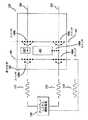
タッチスクリーン220は、複数の駆動線222及び複数の感知線223を有する容量性感知媒体を含むことができるタッチ感知回路を含むことができる。用語「線」とは、当業者には容易に理解されるように、本明細書では単に導電路を指すのに用いる場合があり、厳密に線形である構造体に限定されず、方向を変える経路を含み、及なるサイズ、形状、材料、その他の経路を含む点に留意されたい。駆動線222は、ドライバ論理214から駆動装置インタフェース224を介して誘導信号216により駆動することができ、感知線223において生成された結果として得られる感知信号217は、感知インタフェース225を介してタッチ制御装置206内の感知チャンネル208(事象検出及び復調回路とも呼ばれる)に送信することができる。このように、駆動線及び感知線は、容量性感知ノードを形成するよう相互作用することができるタッチ感知回路の一部とすることができ、該容量性感知ノードは、タッチ画素226及び227などのタッチ画像素子(タッチ画素)と考えることができる。このような捉え方は、タッチスクリーン220がタッチの「画像」を取り込んでいると見なされる場合に特に有用とすることができる。換言すると、タッチスクリーン内の各タッチ画素でタッチが検出されたかどうかをタッチ制御装置206が判断した後、タッチが発生したタッチスクリーン内のタッチ画素のパターンは、タッチの「画像」(例えば、タッチスクリーンに触れている指のパターン)と考えることができる。 The
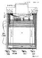
図3は、本開示の実施形態による駆動線222及び感知線223の例示的な構成を示すタッチスクリーン220のより詳細な図である。図3に示すように、各駆動線222は、接続部305にて駆動線リンク303により電気的に接続することができる1つ又はそれ以上の駆動線セグメント301から形成することができる。駆動線リンク303は、感知線223に電気的に接続されておらず、駆動線リンクは、バイパス307を通じて感知線を迂回することができる。駆動線222及び感知線223は、タッチ画素226及び227などのタッチ画素を形成するために容量的に相互作用することができる。駆動線222(すなわち、駆動線セグメント301及び対応する駆動線リンク303)及び感知線223は、タッチスクリーン220において電気回路素子で形成することができる。図3の例示的な構成においては、タッチ画素226及び227の各々は、1つの駆動線セグメント301の一部、感知線223の一部、及び別の駆動線セグメント301の一部を含むことができる。例えば、タッチ画素226は、感知線の部分311の片側の駆動線セグメントの右半部分309、及び感知線の部分311の反対側の駆動線セグメントの左半部分313を含むことができる。 FIG. 3 is a more detailed view of the
回路素子は、例えば、上述のように、従来のLCDディスプレイ内に存在することができる構造体を含むことができる。尚、回路素子は、キャパシタ全体、トランジスタ全体、その他など回路構成部品全体に限定されず、平行板キャパシタの2つのプレートの一方だけなど、回路の一部を含むことができる。図4は、共通電極(Vcom)が本開示の実施形態によるタッチ感知システムのタッチ感知回路の一部を形成することができる、例示的な構成を示している。共通電極は、画像を表示するためにディスプレイシステムの一部として動作することができる、一部の形式の従来のLCDディスプレイ(例えば、広視野角技術(FFS)ディスプレイ)の表示画素のスタックアップ(すなわち、表示画素を形成するスタック材料層)におけるディスプレイシステム回路の回路素子である。図4に示す実施例においては、共通電極(Vcom)401(例えば、図1Dの素子161)は、タッチスクリーン220のディスプレイシステムの表示回路として動作することができ、更に、タッチ感知システムのタッチ感知回路として動作することもできる多機能回路素子の役割を果たすことができる。この実施例においては、共通電極401は、タッチスクリーンの表示回路の共通電極として動作することができ、更に、タッチスクリーンのタッチ感知回路として他の共通電極とグループ化されたときに共に動作することもできる。例えば、共通電極401のグループは、タッチ感知段階中にタッチ感知回路の駆動線又は感知線の容量性部分として共に動作することができる。タッチスクリーン220の他の回路素子は、例えば、領域の共通電極401を共に電気的に接続すること、及び電気的接続部を切り替えること、その他によって、タッチ感知回路の一部を形成することができる。一般に、タッチ感知回路素子の各々は、タッチ感知回路の一部を形成することができ、更に、表示回路の一部を形成するなど1つ又はそれ以上の他の機能を行うことができる多機能回路素子とすることができ、或いは、タッチ感知回路としてのみ動作することができる単機能回路素子とすることができる。同様に、表示回路素子の各々は、表示回路として動作することができ、更に、タッチ感知回路として動作するなど1つ又はそれ以上の他の機能を行うことができる多機能回路素子とすることできる、或いは、表示回路としてのみ動作することができる単機能回路素子とすることができる。従って、幾つかの実施形態においては、表示画素スタックアップにおける回路素子の一部は、多機能回路素子とすることができ、他の回路素子は、単機能回路素子とすることができる。他の実施形態においては、表示画素スタックアップの回路素子の全ては、単機能回路素子であってもよい。 The circuit elements can include structures that can exist in conventional LCD displays, for example, as described above. The circuit element is not limited to the entire circuit component such as the entire capacitor, the entire transistor, or the like, but may include a part of the circuit such as only one of the two plates of the parallel plate capacitor. FIG. 4 illustrates an exemplary configuration in which the common electrode (Vcom) can form part of a touch sensing circuit of a touch sensing system according to an embodiment of the present disclosure. The common electrode can be operated as part of a display system to display an image, a display pixel stackup of some types of conventional LCD displays (eg, wide viewing angle technology (FFS) displays) ( That is, it is a circuit element of a display system circuit in a stack material layer forming a display pixel). In the embodiment shown in FIG. 4, the common electrode (Vcom) 401 (eg, the
加えて、本明細書の例示的な実施形態は、表示回路を表示段階中に動作しているものとして説明することができ、更に、タッチ感知回路をタッチ感知段階中に動作しているものとして説明することができるが、表示段階及びタッチ感知段階は、同時に動作させ、例えばある程度又は完全に重なり合うことができ、或いは、表示段階及びタッチ段階は、異なる時間に動作することができる点を理解されたい。また、本明細書の例示的な実施形態は、特定の回路素子を多機能として説明し、他の回路素子を単機能として説明しているが、他の実施形態においては、回路素子は特定の機能に限定されない点を理解されたい。換言すると、本明細書の1つの例示的な実施形態において単機能回路素子として説明される回路素子は、他の実施形態においては多機能回路素子として構成することができ、逆もまた可能である。 In addition, the exemplary embodiments herein may describe the display circuit as operating during the display phase, and further assume that the touch sensing circuit is operating during the touch sensing phase. As can be appreciated, it is understood that the display phase and touch sensing phase can be operated simultaneously, eg, to some extent or completely overlap, or the display phase and touch phase can be operated at different times. I want. In addition, although the exemplary embodiments of the present specification describe specific circuit elements as multi-functions and other circuit elements as single functions, in other embodiments, circuit elements are specified as specific functions. It should be understood that it is not limited to functions. In other words, a circuit element described as a single function circuit element in one exemplary embodiment herein may be configured as a multi-function circuit element in other embodiments, and vice versa. .
例えば、図4は、一般に駆動線セグメント301及び感知線223にそれぞれ対応する駆動領域セグメント301及び感知線223を形成するよう共にグループ化された共通電極401を示している。表示画素の多機能回路素子を1つの領域にグループ化することは、表示画素の多機能回路素子を共に動作させて、当該領域の共通機能を実行することを意味することができる。機能地域へのグループ化は、例えば、システムの構造的構成(例えば、物理的破断及びバイパス、電圧線構成)、システムの動作上の構成(例えば、回路素子のオン/オフ切り替え、電圧レベル及び/又は電圧線上の信号の変更)など、1つの手法又は手法の組み合わせにより達成することができる。 For example, FIG. 4 shows
幾つかの実施形態においては、回路素子のグループ化は、表示画素のレイアウトとして実施することができ、各表示画素は、表示画素構成の限定された数のセットから選択される。幾つかの実施形態においては、タッチ感知回路の特定の機能は、その機能を実行することができる構成を有する特定の形式の表示画素により提供することができる。例えば、図17〜図22を参照して以下で説明する1つの実施形態は、スタックアップの接続層内で1つ又はそれ以上の隣接画素を共に接続することができる形式の表示画素、スタックアップの別の層に対する接点を提供することができる形式の表示画素、及び他の層内で1つ又はそれ以上の隣接画素を共に接続することができる形式の表示画素を含むことができる。 In some embodiments, grouping of circuit elements can be implemented as a display pixel layout, with each display pixel being selected from a limited number of sets of display pixel configurations. In some embodiments, a particular function of the touch sensing circuit can be provided by a particular type of display pixel that has a configuration capable of performing that function. For example, one embodiment described below with reference to FIGS. 17-22 is a display pixel of the type that can connect one or more adjacent pixels together in a stack-up connection layer, a stack-up. Display pixels of a type that can provide a contact to another layer of the display, and display pixels of a type that can connect one or more adjacent pixels together in other layers.
幾つかの実施形態においては、領域は、例えば、画素を異なるサイズ、形状、その他の領域にグループ化できるように再構成可能にすることができる。例えば、一部の実施形態は、例えば、タッチスクリーンから感知されることになる物体の環境騒音、サイズ及び/又は距離の変動に応じて、異なるサイズの領域に表示画素をグループ化する再構成可能なスイッチング方式を可能にするプログラマブルスイッチングアレイを含むことができる。グループ化を可能にすることができる構成の他の態様は、再構成可能ではない場合があり、例えば、表示画素のスタックアップ内の線の物理的破断は再構成可能ではない。しかしながら、物理的破断を含むタッチスクリーン構成は、例えば、プログラマブルスイッチ、信号発生器、その他など、再構成可能である他の回路素子を含めることによって異なるサイズ、形状、その他の領域への表示画素の再構成可能なグループ化を依然として可能にすることができる。 In some embodiments, the regions can be reconfigurable, for example, so that the pixels can be grouped into different sizes, shapes, and other regions. For example, some embodiments may be reconfigurable to group display pixels into different sized regions, for example, depending on environmental noise, size and / or distance variations of objects that will be sensed from a touch screen A programmable switching array can be included that allows for a simple switching scheme. Other aspects of configurations that can enable grouping may not be reconfigurable, for example, physical breaks of lines in the display pixel stackup are not reconfigurable. However, touch screen configurations that include physical breaks, for example, display pixels to different sizes, shapes, and other areas by including other circuit elements that are reconfigurable, such as programmable switches, signal generators, etc. Reconfigurable grouping can still be possible.
タッチスクリーンの表示画素の多機能回路素子は、表示段階及びタッチ段階の両方で動作することができる。例えば、タッチ段階中に、共通電極401は、駆動領域及び感知領域のようなタッチ信号線を形成するように共にグループ化することができる。幾つかの実施形態においては、回路素子は1つの形式の連続的タッチ信号線及び別の形式のセグメント化されたタッチ信号線を形成するようにグループ化することができる。例えば、図4は、駆動領域セグメント403及び感知領域405がタッチスクリーン220の駆動線セグメント301及び感知線223に対応する1つの例示的な実施形態を示している。例えば、他の実施形態においては他の構成が可能であり、駆動線が各々連続した駆動領域から形成され、感知線が各々、駆動領域を迂回する接続部を介して共にリンクされる複数の感知領域セグメントから形成されるように、共通電極401を共にグループ化することができる。例示的な表示段階及び例示的なタッチ段階の動作の更なる詳細を図11A〜図11Bを参照して以下で説明する。 The multifunction circuit element of the display pixel of the touch screen can operate in both the display stage and the touch stage. For example, during the touch phase, the
図3の実施例の駆動領域は、表示画素の複数の共通電極を含む矩形領域として図4に示されており、図3の感知領域は、LCDの垂直方向の長さを延びる表示画素の複数の共通電極を含む矩形領域として図4に示されている。幾つかの実施形態においては、図4の構成のタッチ画素は、例えば、表示画素の64x64区域を含むことができる。しかしながら、駆動領域及び感知領域は、図示の形状、方位及び位置に限定されず、本開示の実施形態によるあらゆる好適な構成を含むことができる。タッチ画素を形成するのに使用される表示画素は、上述したものに限定されず、本開示の実施形態によるタッチ能力を可能にするあらゆる好適なサイズ又は形状とすることができる点を理解されたい。 The drive region of the embodiment of FIG. 3 is shown in FIG. 4 as a rectangular region including a plurality of common electrodes of display pixels, and the sensing region of FIG. 3 is a plurality of display pixels extending in the vertical direction of the LCD. FIG. 4 shows a rectangular region including the common electrodes. In some embodiments, a touch pixel in the configuration of FIG. 4 can include, for example, a 64 × 64 area of display pixels. However, the drive region and the sensing region are not limited to the shape, orientation, and position shown, and may include any suitable configuration according to embodiments of the present disclosure. It should be understood that the display pixels used to form the touch pixels are not limited to those described above, and can be any suitable size or shape that allows for touch capabilities according to embodiments of the present disclosure. .
図5は、本開示の実施形態に従って、共通電極401を図4に示す領域にグループ化し、更に、駆動領域セグメントをリンクして駆動線を形成するのに使用することができる導電線の例示的な構成を示す。一部の実施形態は、図13に示す例示的な実施形態に示すように、駆動線間及び/又は駆動線と感知線との間の接地領域など、他の領域を含むことができる。 FIG. 5 illustrates exemplary conductive lines that can be used to group
図5は、x方向に沿った複数のxVcom線501と、y方向に沿った複数のyVcom線503とを示す。この実施形態においては、共通電極401の各横列は、対応するxVcom線501を有することができ、共通電極401の各縦列は、対応するyVcom線503を有することができる。図5は更に、複数の駆動領域セグメント403(破線で示す)を示しており、各駆動領域セグメント403は、x−y−com接続部505を介して共に接続された共通電極401のグループとして形成することができ、x−y−com接続部505は、以下で更に詳細に説明するように、駆動領域セグメント内でxVcom線501及びyVcom線503に各共通電極を接続する。yVcom線503aのような、駆動領域セグメント403を延びるyVcom線503は、他の駆動領域セグメント(例えば、所与の駆動領域セグメントを上回る及び下回るセグメント)から各駆動領域セグメントの電気的分離を行う破断部509を含むことができる。破断部509は、y−切断(y方向の電気的切断)を行うことができる。 FIG. 5 shows a plurality of
駆動線511は各々、複数の駆動領域セグメント403により形成することができ、該セグメントは、共通電極401及び相互接続導電線xVcomにより形成することができる。具体的には、駆動線511は、xVcom線501を使用して感知領域405にわたって駆動領域セグメント403を接続することにより形成することができる。図5に示すように、第1の駆動線511aは、駆動領域セグメント403の最上横列により形成することができ、次の駆動線511bは、駆動領域セグメント403の次の横列により形成することができる。xVcom線は、以下で更に詳細に説明するように、バイパス513を使用して感知領域405内のyVcom線を迂回する導電路である。 Each
図5は更に、複数の感知領域405(破線により示す)を示す。各感知領域405は、y−com接続部507を介して共に接続された共通電極401のグループとして形成することができ、y−com接続部507は、yVcom線503のうちの1つに感知領域405の各共通電極を接続することができる。更なる接続部(例えば図10を参照)は、各感知領域405のyVcom線を共に接続することができる。例えば、更なる接続部は、動作のタッチ段階中に各感知領域のyVcom線を共に接続することができるタッチスクリーン220の境界部においてスイッチを含むことができる。yVcom線503bのように、感知領域405を介して延びるyVcom線503は、y方向で共通電極401の全てを電気的に接続することができ、従って、感知領域のyVcom線は破断部を含まない。このようにして、例えば、感知領域は、互いに及び対応する表示画素の回路素子に接続された複数の垂直共通電圧線yVcomにより形成することができ、その結果、感知領域内の表示画素の電気的接続の回路素子からなる感知線512が形成される。図5に示す例示的な感知領域においては、垂直共通電圧線yVcomは、水平共通電圧線xVcomと非接続状態にすることができ、更に、容量性タッチ感知の構造体を形成するように水平共通電圧線xVcom(513で)上を横断することができる。yVcom及びxVcom上のこの横断はまた、感知領域と駆動領域との間で更なる寄生キャパシタンスを形成することもできる。 FIG. 5 further shows a plurality of sensing areas 405 (shown by dashed lines). Each
各共通電極401は、表示画素515及び517など、タッチスクリーン220の表示画素に対応することができる。表示段階中に、共通電極401は、タッチスクリーン上で画像を表示するように、タッチスクリーン220のディスプレイシステムの表示回路として他の表示画素構成部品と共に動作することができる。タッチ段階中に、共通電極401のグループは、タッチスクリーン220のタッチ感知システムのタッチ感知回路として動作し、タッチスクリーン上又はその近傍で1つ又はそれ以上のタッチを検出することができる。 Each
タッチ段階中の動作において、水平共通電圧線xVcom 501は、誘導信号を送信して駆動線511を誘導し、誘導された駆動線と感知線512との間に電場を形成して、図3のタッチ画素226などのタッチ画素を生成することができる。指などの物体がタッチ画素に接近又はタッチすると、物体は、駆動線511と感知線512との間に延在する電場に影響を与え、その結果、感知線に容量結合された電荷量を低減することができる。電荷の低減は、感知チャンネルにより感知され、タッチの「画像」を作成するために、他のタッチ画素の類似情報と共にメモリ内に格納することができる。 In operation during the touch phase, the horizontal common
幾つかの実施形態においては、駆動線及び/又は感知線は、例えば典型的なLCDディスプレイ内に既に存在している他の構造体(例えば、搬送信号、格納電圧、その他など、典型的なLCDディスプレイ内で回路素子としても機能する、他の電極、導電層及び/又は半導電層、金属線)、典型的な液晶スタックアップ構造体でない液晶スタックアップ内に形成される他の構造体(例えば、機能が実質的にタッチスクリーンのタッチ感知システム用のものである他の金属線又はプレート)、及び液晶スタックアップの外側に形成される構造体(例えば、外部の実質的に透明な導電プレート、ワイヤ及び他の構造体など)を含む、他の構造体で形成することができる。例えば、タッチ感知システムの一部は、公知のタッチパネルオーバレイに類似した構造体を含むことができる。ディスプレイ内に既に存在する構造体を部分的に又は全て使用してタッチ感知システムを形成すると、典型的にはディスプレイを覆うことになるタッチ感知に主として専用の構造体の量を低減することによって、タッチスクリーンの画質、輝度、その他を場合によっては増大させることができる。 In some embodiments, the drive lines and / or sense lines are typical LCDs, such as other structures already present in a typical LCD display (eg, carrier signals, stored voltages, etc.). Other electrodes, conductive layers and / or semiconductive layers, metal lines) that also function as circuit elements in the display, other structures formed in a liquid crystal stackup that is not a typical liquid crystal stackup structure (e.g. , Other metal lines or plates whose function is substantially for touch-screen touch sensing systems), and structures formed outside the liquid crystal stackup (eg, external substantially transparent conductive plates, Other structures, including wires and other structures). For example, a portion of the touch sensing system can include a structure similar to a known touch panel overlay. Forming a touch sensing system using part or all of the structures already present in the display typically reduces the amount of structures primarily dedicated to touch sensing that would cover the display, The image quality, brightness, etc. of the touch screen can be increased in some cases.
幾つかの実施形態においては、表示画素は、駆動領域と感知領域との間の領域及び/又は2つの駆動領域間にグループ化することができ、例えば、これらの領域は、接地又は仮想接地に接続され、駆動領域の間及び/又は駆動領域と感知領域との間の干渉を更に最小限に抑えるように接地領域を形成することができる。図13A〜図13Bは、駆動領域間、及び駆動領域と感知領域との間の接地領域を含む、本開示の実施形態による領域の例示的なレイアウトを示す。他の実施形態においては、垂直共通電圧線破断部を省略し、駆動領域間で全体的に線を共有することができる。 In some embodiments, display pixels can be grouped between a drive region and a sensing region and / or between two drive regions, for example, these regions can be grounded or virtual grounded. The ground region can be formed to be connected and to further minimize interference between drive regions and / or between drive regions and sensing regions. 13A-13B illustrate an exemplary layout of regions according to embodiments of the present disclosure, including ground regions between drive regions and between drive regions and sensing regions. In other embodiments, the vertical common voltage line break may be omitted and the line may be shared between the drive regions as a whole.
図5でわかるように、表示画素515は、感知領域405にグループ化することができ、更に、表示画素517は、駆動領域セグメント403にグループ化することができる。図6〜図8は、図5の「ボックスA」内の表示画素515及び517の更なる詳細を示す平面図及び側面図を示しており、本開示の実施形態による、面内/層内である例示的な破断部/バイパスと、面外/層外である例示的な破断部/バイパスとを含む1つの例示的な構成を示す。 As can be seen in FIG. 5, the
図6は、本開示の実施形態による、タッチスクリーン220の表示画素515及び517並びに他の構造体の更なる詳細を示す、図5の「ボックスA」の拡大図である。表示画素515及び517は各々、共通電極401及び3つの表示画素電極601を含むことができ、3つの表示画素電極601は各々、タッチスクリーンの表示段階中にゲート線611全体にわたって印加された電圧によりサブ画素のトランジスタ609がオンになったときにサブ画素に色データを提供する、Rデータ線603、Gデータ線605及びBデータ線607に対応する、赤色(R)サブ画素、緑色(G)サブ画素及び青色(B)サブ画素である。 FIG. 6 is an enlarged view of “Box A” of FIG. 5 showing further details of
幾つかの実施形態においては、モノクローム(例えば、白黒)表示画素、3つより多い又は少ないサブ画素を含む表示画素、赤外線など非可視スペクトルで動作する表示画素、その他など、他の形式の表示画素を使用することができる。異なる実施形態は、異なるサイズ、形状、光学的性質を有する表示画素を含むことができる。一部の実施形態の表示画素は、互いに対して異なるサイズ、形状、光学的性質、その他のものとすることができ、タッチスクリーンにおいて利用される異なる形式の表示画素は、幾つかの実施形態においては異なる機能を提供することができる。 In some embodiments, other types of display pixels, such as monochrome (eg, black and white) display pixels, display pixels that include more or less than three sub-pixels, display pixels that operate in a non-visible spectrum such as infrared, and the like. Can be used. Different embodiments can include display pixels having different sizes, shapes, and optical properties. The display pixels of some embodiments can be different sizes, shapes, optical properties, etc. relative to each other, and the different types of display pixels utilized in touch screens are in some embodiments. Can provide different functions.
図6はまた、表示画素517を延びるyVcom線503が、表示画素517(及び表示画素517の駆動領域セグメント403、図5を参照)を隣接する駆動領域セグメントから分離する破断部509を有することを示している。破断部509は、実質的に同一平面、この場合は、yVcom線503が延びるx−y面において延びた導電路間の電気的開口部である面内破断部の実施例である。同様に、破断部509は、同一層、この場合は、以下で説明するように第2の金属層に延びる導電路間の電気的開口部である層内破断部の実施例である。多くの層内破断部も面内破断部とすることできるが、これは必ずしも当てはまる訳ではない。例えば、スタックアップ内の材料層の導電路の破断部は、異なるスタックアップ高さ(すなわち、異なる平面)にて層が形成される場所で発生する可能性があり、従って、このような場所での破断部は、層内面外破断部ではなく、層内面内破断部となる。 6 also shows that the
これに反して、感知領域405の表示画素515を通って延びるyVcom線503は破断部を含まず、その結果、表示画素515は、y方向で感知領域405の他の表示画素に電気的に接続することができ、すなわち、感知領域の表示画素はy接続される。 On the other hand, the
xVcom線501は、表示画素515及び517を通ってx方向に延びる。xVcom線501は、表示画素515の左上コーナのRデータ線603の背後のxVcomの拡大図で示すように、それぞれR、G及びBデータ線603、605及び607の背後にある。xVcom及びyVcom線間の接続部、並びに表示画素515及び517の共通電極401は、図6に分解図で更に詳細に示されており、図6はまた、xVcom線501がyVcom線503の背後にあり、yVcom線503が共通電極401の背後にあることを示している。感知領域の表示画素515については、表示画素515のy−com接続507の分解図は、y−com接続が表示画素のyVcom線503と共通電極401との間の導電線613(例えば、導電性材料が充填されたバイア)であることを示し、Vcom線501とyVcom線503との間には接続部がなく(従って、xVcom線と共通電極との間には接続部がない)、すなわち、バイパス513があることを示す。バイパス513の結果として、表示画素515は、x切断又はx方向で隔離され、すなわち、x方向に沿って隣接する表示画素から切断又は隔離することができる。この例示的な実施形態においては、上述の境界部スイッチなど、感知領域のyVcom線503の更なる接続部は、表示画素515の左側の隣接する感知領域表示画素の共通電極に表示画素515の共通電極401を電気的に接続し、従って、バイパス513は、表示画素515右側の隣接駆動領域表示画素517から表示画素515を「右側切断する」(換言すると、表示画素515を正のx方向に表示画素からx切断、すなわち、正のx切断をすることができる。 The
バイパス513は、実質的に異なる平面内に延びる導電路間の電気開口部とすることができる面外バイパスの実施例であり、この場合、yVcom線503が延びるx−y平面は、xVcom線501が延びるx−y平面とは異なる場合がある。同様に、以下で説明するように、バイパス513は、異なる層、この場合は、yVcom503の第2の金属層及びxVcom501の第1の金属層に延びる導電路間の電気開口部とすることができる層外バイパスの実施例である。yVcom−共通電極の接続部、タッチスクリーン境界部(上述のように、同じ感知領域のyVcom線における)内のyVcom−yVcomの接続部、及びxVcomとyVcom線との間のバイパスを含むこの構成は、感知領域内でディスプレイの回路素子を共にグループ化してタッチ感知に対する感知線を形成し、更に、感知領域によって互いに分離された駆動領域セグメントを共にリンクさせるxVcom線で感知線を迂回して、タッチ感知に対する駆動線を形成する1つの実施例である。
駆動領域セグメントの表示画素517において、表示画素517のx−y−com接続部505の分解図は、x−y−com接続部が、xVcom線をyVcom線に接続する導電線615並びにyVcom線を共通電極に接続する導電線613のうちの1つを含むことができることを示している。従って、各表示画素が、垂直線(yVcom)(すなわちy接続)及び水平線(xVcom)(すなわち、x接続)の同じ導電グリッドに接続することができるので、駆動領域セグメントにおける各表示画素の共通電極は、共に電気的に接続することができる。この例示的な構成においては、共通電極、垂直線及び水平線は、実質的に同一平面の異なる平面に配向され、2つのセットの接続部を介して共に接続することができ、一方のセットが垂直線及び水平線を接続し、他方のセットが垂直線及び共通電極を接続する。垂直線内の破断部を含むこの構成は、駆動領域セグメント内でディスプレイの回路素子を共にグループ化し、中間感知線を迂回する駆動線リンクを介して他の駆動線セグメントにリンクすることができる駆動線のタッチ感知回路を形成する1つの実施例である。 In the
図7〜図8は、それぞれ、表示画素515スタックアップの一部及び表示画素517スタックアップの一部を示す断面図である。図7は、図6の7−7’から矢印線に沿って切り取った表示画素515の断面図を示す。図7は、第1の金属層(M1)に形成されたゲート線611及びxVcom線501、Bデータ線607、ドレイン701、及び第2の金属層(M2)内に形成されたyVcom線503を含む。この図はまた、共通電極401と、ITOなど透明導体から形成された表示画素電極601とを含む。共通電極401は、導電性材料を充填することができる誘電体層707a内のバイア、すなわち、図6の導電線613の1つの実施例である導電性バイア703を介してyVcom線503に電気的に接続することができる。図7はまた、xVcom501とyVcom503との間のバイパス513(接続なし)を示している。この点に関して、バイパス513は、誘電体層707bの一部を含むことができる、xVcom501及びyVcom503を分離する構造体とみなすことができる。ゲート絶縁体層705は、Si02、SiNx、その他などの誘電材料を含むことができる。液晶層は、画素電極に続くカラーフィルタの上方に配置することができ、偏光板は、スタックアップ(図示せず)の上部及び底部に位置決めすることができる。タッチスクリーンは図7に関しては上部から見える。 7 to 8 are cross-sectional views showing a part of the
図8は、図6の8−8’から矢印線に沿って取った表示画素517の断面図を示す。図8は、図8の導電性バイア801が図7のバイパス513と置き換わっていることを除いて、図7と同一である。よって、xVcom 501は、駆動領域セグメント表示画素517内のyVcom503に電気的に接続することができる。従って、図6の導電線615は、この例示的なスタックアップにおいて導体充填バイアとすることができる。 FIG. 8 shows a cross-sectional view of the
これらを総合すると、図7〜図8は、幾つかの実施形態において、本開示の実施形態による面外/層外破断部/バイパスを使用することによって、多機能回路素子を含む多機能タッチ感知LCD構造体を生成する効率的な方法がどのようにして得られるかに関する1つの実施例を示している。この場合、幾つかの実施形態において、異なる平面/層内の導電路間に作製された接続部/バイパスは、多機能構成の設計においてより多くの選択肢を提供することができ、他の場合では同一平面/層内にバイパスを形成するために追加する必要がある付加的な構造体(例えば、線)の数を低減できる場合がある。この点に関して、一部の実施形態におけるy−切断部及び/又はx−切断部は、例えば、表示画素スタックアップの異なる平面/層内に単に導電路を形成することによって好都合に形成することができる。同様に、一部の実施形態におけるy−接続部及び/又はx−接続部は、異なる平面/層内の導電路を接続するために異なる平面/層間に導電路を使用して好都合に形成することができる。特に、これによって、本開示の実施形態による一体型タッチ機能を追加するために既存の液晶設計をより容易に修正可能にすることができる。この点に関しては、面内/層内及び面外/層外破断部及びバイパスを選択的に使用することで、既存のLCD設計においてより多くの構造体をタッチ感知システムの回路素子として使用することが可能になり、マスキング、ドーピング、堆積、その他など、既存の製造工程に必要とされる変更の数を低減することができる。 Taken together, FIGS. 7-8 show, in some embodiments, multifunction touch sensing including multifunction circuit elements by using out-of-plane / out-of-layer breaks / bypasses according to embodiments of the present disclosure. Fig. 4 illustrates one example of how an efficient method of generating an LCD structure can be obtained. In this case, in some embodiments, connections / bypasses created between conductive paths in different planes / layers can provide more options in the design of multi-functional configurations, in other cases It may be possible to reduce the number of additional structures (eg, lines) that need to be added to form a bypass in the same plane / layer. In this regard, the y-cut and / or x-cut in some embodiments may be conveniently formed, for example, simply by forming conductive paths in different planes / layers of the display pixel stackup. it can. Similarly, y-connections and / or x-connections in some embodiments are advantageously formed using conductive paths between different planes / layers to connect conductive paths in different planes / layers. be able to. In particular, this can make existing liquid crystal designs more easily modifiable to add an integrated touch function according to embodiments of the present disclosure. In this regard, more structures can be used as circuit elements in touch sensing systems in existing LCD designs by selectively using in-plane / in-layer and out-of-plane / out-of-layer breaks and bypasses. Can be reduced and the number of changes required in existing manufacturing processes, such as masking, doping, deposition, etc., can be reduced.
例示的なタッチスクリーン及び多機能タッチスクリーンLCD回路素子を動作させる例示的な方法の更なる詳細を図9〜図12Bを参照して説明する。図9は、本開示の実施形態による複数のサブ画素を含む、例示的なタッチスクリーン900の部分回路図である。上述の例示的な実施形態と同様に、タッチスクリーン900のサブ画素は、LCDサブ画素及びタッチセンサ回路素子として多機能性が可能であるように構成することができる。すなわち、サブ画素は、表示画素のLCD回路の一部として動作することができ、更に、タッチ感知回路の回路素子として動作することもできる回路素子を含むことができる。このように、タッチスクリーン900は、一体型タッチ感知能力を有するLCDとして動作することができる。図9は、タッチスクリーン900のサブ画素901、902及び903の詳細を示す。この例示的な実施形態においては、各サブ画素は、赤色(R)、緑色(G)又は青色(B)サブ画素とすることができ、3つのR、G及びBサブ画素全ての組み合わせが1つの色表示画素を形成する。この例示的な実施形態は、赤、緑、及び青のサブ画素を含むが、サブ画素は、電磁放射線の他の色の光又は他の波長(例えば、赤外線)に基づくことができ、或いは、単色構成に基づいてもよい。 Further details of exemplary methods of operating exemplary touch screens and multi-function touch screen LCD circuit elements are described with reference to FIGS. 9-12B. FIG. 9 is a partial circuit diagram of an
サブ画素902は、ゲート955a、ソース955b及びドレイン955cを有する薄膜トランジスタ(TFT)955を含むことができる。サブ画素902はまた、例えば、図6に示す共通電極401など、サブ画素901、902及び903の間で共有される実質的に導電性の材料の連続プレートとすることができる共通電極(Vcom)957bを含むことができる。サブ画素902はまた、ディスプレイシステム回路の一部として共通電極957bと共に動作することができる画素電極957aを含むことができる。画素電極957aは、例えば、図6〜図8に示す画素電極601とすることができる。タッチスクリーン900は、各サブ画素の画素電極及び共通電極が、サブ画素の液晶に適用されるフリンジフィールドを生成するFFSディスプレイシステムとして動作することができ、更に、サブ画素のストレージキャパシタを形成することができる。サブ画素902は、画素電極957a及び共通電極957bにより形成されたストレージキャパシタ957を含むことができる。サブ画素902はまた、緑色(G)の色データのGデータ線917におけるデータ線の一部917a、及びゲート線913における一部913bを含むこともできる。ゲート955aは、ゲート線部913bに接続することができ、ソース955bは、Gデータ線部917aに接続されている。画素電極957aは、TFT955のドレイン955cに接続することができる。 The sub-pixel 902 can include a thin film transistor (TFT) 955 having a
サブ画素901は、ゲート905a、ソース905b及びドレイン905cを有する薄膜トランジスタ(TFT)905を含むことができる。サブ画素901はまた、サブ画素に対するフリンジフィールドを生成し、更に、ストレージキャパシタ907を形成するために共通電極957bと共に動作することができる画素電極907aを含むことができる。サブ画素901はまた、赤色(R)の色データ用データ線であるRデータ線915の一部915a、及びゲート線913の一部913aを含むことができる。ゲート905aは、ゲート線部913aに接続することができ、ソース905bは、Rデータ線部915aに接続することができる。画素電極907aは、TFT905のドレイン905cに接続することができる。サブ画素901及び902は、例えば、従来のLCDサブ画素の構造体の大部分又は全てを含むことができる。 The sub-pixel 901 can include a thin film transistor (TFT) 905 having a
サブ画素903は、ゲート975a、ソース975b及びドレイン975cを有する薄膜トランジスタ(TFT)975を含むことができる。サブ画素903はまた、サブ画素に対するフリンジフィールドを生成し、更に、ストレージキャパシタ977を形成するために共通電極957bと共に動作することができる画素電極977aを含むことができる。サブ画素903はまた、青色(B)の色データ用データ線であるBデータ線919の一部919a、及びゲート線913の一部913cを含むことができる。ゲート975aは、ゲート線部913cに接続することができ、ソース975bは、Bデータ線部919aに接続することができる。画素電極977aは、TFT975のドレイン975cに接続することができる。サブ画素901及び902とは異なり、サブ画素903はまた、y方向に延びる共通電圧線であるyVcom925の一部925a、及び接続点929を含むことができる。他の実施形態においては、yVcomは、青色サブ画素ではなく赤色サブ画素又は緑色サブ画素に延びることができる。図6を参照して上述したy−com接続507、又はx−y−com接続部505などの接続部は、例えば、共通電極957bをyVcom925(他の表示画素を介して垂直方向に延びる)に接続するため、共通電極957bをyVcom925及びxVcom921(他の画素を介して水平方向に延びる)に接続するため、及びその他のために、接続点929において作製することができる。このようにすると、例えば、共通電極957bは、接続される共通電極の領域を作成するために他の表示画素の共通電極と接続することができる。 The sub-pixel 903 can include a thin film transistor (TFT) 975 having a
別個の領域を作成する1つの方法は、幾つかの例示的な実施形態において上述したように、水平及び/又は垂直共通線内に破断部(開口部)を形成することによるものである。例えば、yVcom925は、図9に示すような任意選択的な破断部を有することができ、これにより、破断部の上方のサブ画素と破断部の下方のサブ画素とを分離可能にすることができ、すなわち、サブ画素は、底部切断することができる。x−切断部は、接続点929にてx−y−com接続部の代わりにy−com接続部を形成することにより作成することができ、従って、xVcom921が共通電極957bから切断される。幾つかの実施形態においては、xVcom921は、破断部を含むことができ、該破断部は、破断部の右側のサブ画素を破断部の左側のサブ画素から隔離可能にすることができる。他の構成は、感知線のバイパスを介して共にリンクされた駆動線セグメントに関して上述されたように、表示画素回路素子をグループ化可能にすることができる。 One method of creating separate regions is by forming breaks (openings) in the horizontal and / or vertical common line, as described above in some exemplary embodiments. For example, the
このようにすると、タッチスクリーン900の共通電極を共にグループ化して、タッチ感知システムのタッチ感知回路の一部として動作することができる表示画素内の構造体を形成することができる。例えば、共通電極は、幾つかの実施形態などに関して上述されたようにバイパス及びリンクを形成するために駆動領域又は感知領域を形成するように構成することができる。この点に関しては、共通電極、xVcom線、その他の回路素子は、多機能回路素子として動作することができる。 In this way, the common electrodes of the
一般に、タッチスクリーン900は、画面内の全てのサブ画素の共通電極が、例えば、複数の水平共通電圧線に対する接続部を有する少なくとも1つの垂直共通電圧線を介して共に接続できるように構成することができる。別のタッチスクリーンは、異なるグループのサブ画素を共に接続して、共に接続された共通電極の複数の別個の領域を形成できるように構成することができる。 In general, the
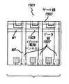
図10〜図12bを参照し、本開示の実施形態によるタッチ感知動作を説明する。図10は、本開示の実施形態による、例示的なタッチスクリーンの駆動領域1001及び感知領域1003における表示画素内のタッチ感知回路の一部の部分回路図を示す。簡潔さを期すために、図10は、一部の回路素子がタッチ感知回路でなく主として表示回路の一部として動作することを表すために、破線で示した回路素子を含む。加えて、タッチ感知動作は、主として、単一の駆動表示画素1001a(例えば、駆動領域1001の単一の表示画素)と単一の感知表示画素1003a(例えば、感知領域1003の単一の表示画素)とに関して説明している。しかしながら、駆動領域1001内の他の駆動表示画素は、駆動表示画素1001に関して以下に説明するのと同じタッチ感知回路を含むことができ、感知領域1003内の他の感知表示画素は、感知表示画素1003aに関して以下に説明するのと同じタッチ感知回路を含むことができることは理解される。従って、駆動表示画素1001a及び感知表示画素1003aの動作の説明は、それぞれ駆動領域1001及び感知領域1003の動作の説明と考えることができる。 A touch sensing operation according to an embodiment of the present disclosure will be described with reference to FIGS. FIG. 10 illustrates a partial circuit diagram of a portion of a touch sensing circuit in a display pixel in an exemplary touch screen drive region 1001 and sensing region 1003, according to an embodiment of the present disclosure. For the sake of brevity, FIG. 10 includes circuit elements shown in broken lines to indicate that some circuit elements operate primarily as part of the display circuit rather than the touch sensing circuit. In addition, the touch sensing operation mainly includes a single
図10を参照すると、駆動領域1001は、駆動表示画素1001aを含む複数の駆動表示画素を含む。駆動表示画素1001aは、TFT1007、ゲート線1011、データ線1013、xVcom線部1015及びyVcom線部1017、画素電極1019、並びに共通電極1023を含む。図10は、xVcom線部1015及びyVcom線部1017を介して駆動領域1001内の他の駆動表示画素の共通電極に接続されて、以下で更に詳細に説明するようにタッチ感知に使用される構造体を駆動領域1001の表示画素内に形成する共通電極1023を示している。感知領域1003は、感知表示画素1003aを有する複数の感知表示画素を含む。感知表示画素1003aは、TFT 1009、ゲート線1012、データ線1014、yVcom線部1016、画素電極1021及び共通電極1025を含む。図10は、例えばタッチスクリーンの境界部領域内に接続することができるyVcom線部1016を介して感知領域1003内の他の感知表示画素の共通電極に接続されて、以下で更に詳細に説明するようにタッチ感知に使用される構造体を感知領域1003の表示画素内に形成する共通電極1025を示している。 Referring to FIG. 10, the drive region 1001 includes a plurality of drive display pixels including a
タッチ感知段階中に、xVcom線部1015に適用される駆動信号は、駆動領域1001の接続された共通電極1023の構造体と、電荷増幅器1026などの感知増幅器に接続されている感知領域1003のうちの接続された共通電極1025の構造体との間に電界を発生する。電荷が感知領域1003の接続された共通電極の構造体に注入され、電荷増幅器1026は、注入電荷を測定可能な電圧に変換する。注入される電荷の量及びその結果として測定される電圧は、指1027などのタッチ物体の駆動領域及び感知領域への近接度に左右される可能性がある。このようにすると、測定電圧は、タッチスクリーン上又はその近傍でのタッチの指標とすることができる。 During the touch sensing stage, a driving signal applied to the
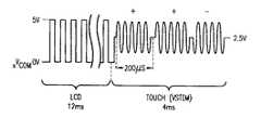
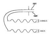
図11Aは、例示的なLCD又は表示段階中及び例示的なタッチ段階中において、駆動表示画素1001を含む駆動領域1001の駆動表示画素にxVcom1015を介して印加された例示的な信号を表している。LCD段階中、xVcom1015及びyVcom1017は、LCD反転を行うために2.5V±2.5Vの方形波信号で駆動させることができる。LCD段階は持続時間が12msである。 FIG. 11A represents an exemplary signal applied via
タッチ段階においては、xVcom1015は、正弦波、方形波、三角波、その他などのAC信号で駆動させることができる。図11Aに示す実施例において、yVcom1016が図11Bに示すように電荷増幅器1026の仮想接地に維持されている間、xVcomは、各々が200マイクロ秒継続する15〜20回の連続誘導段階で駆動させることができる。この場合の駆動信号は、各々が同じ周波数及び0度又は180度(図11Aの「+」及び「−」に対応)の相対位相を有する2.5V±2Vの方形又は正弦波信号とすることができる。タッチ段階は持続時間が4msである。 In the touch stage, the
図12Aは、タッチ段階中の共通電極1023の動作の詳細を示す。特に、共通電極1023及び画素電極1019により形成されるストレージキャパシタのキャパシタンスは、システム内の他のキャパシタンス(すなわち、種々の導電構造体間及び共通電極と指1027との間の浮遊容量)よりも遙かに高いので、共通電極1023に適用されている2.5V±2V正弦駆動信号のAC成分のほとんど全部(約90%)は、画素電極1019にも印加される。従って、共通電極1023と画素電極1019との間の電圧差を小さく維持することができ、液晶は、タッチ誘導に起因する電場の変化が最小であり、LCD段階中に設定された電荷状態を維持する。共通電極1023及び1025は、LCDの表示段階動作中に、通常0又は5ボルトDC(正方形波2.5±2.0V)に帯電することができる。しかしながら、タッチモード中に、駆動領域1023内の共通電極は、2V振幅の重畳正弦波信号で2.5VのDC電圧に帯電することができる。同様に、感知領域1025内の共通電極は、2.5ボルトのDCレベルで電荷増幅器1026の仮想接地に維持することができる。タッチ段階中、駆動領域1001内の共通電極1023上の正弦波信号は、感知領域1003の共通電極1025を通過することができる。駆動領域及び感知領域両方における共通画素電極間の結合が高いことに起因して、共通電極の電圧変化の90%が対応する画素電極に伝達され、従って、タッチ感知を実施している間に表示段階中に保存された画像電荷の変動が最小限に抑えられる。このようにすると、駆動領域及び感知領域の共通電極は、LCD画像に影響を与えることなく、容量性タッチ感知用の構造体を形成することにより、タッチ感知回路の回路素子として動作することができる。 FIG. 12A shows details of the operation of the
共通電極及び画素電極がタッチ感知回路の回路素子として動作するように構成されると同時に、電極は、LCDシステムの一部として継続して動作することができる。図12A〜図12Bに示すように、画素電極1021の構造体の電圧は各々、約±2Vで変調されるが、画素電極1021と共通電極1025との間の相対電圧は、ほぼ一定値±0.1Vのままである。この相対電圧は、LCD動作において表示画素の液晶に発生する電圧であり、その大きさが画像(例えば図12Aでは、この相対電圧は2V)のグレースケールレベルを決定付けることができる。AC変動は通常、液晶の応答時間よりも高い周波数を有するので、タッチ(感知)段階中の相対電圧の0.1VAC変動のLCDに及ぼす影響は、許容可能な程度に低いことになる。例えば、誘導信号周波数、すなわち、AC変動の周波数は通常は100kHzを上回ることになる。しかしながら、液晶の応答時間は通常、100Hzを下回る。従って、タッチシステムの回路素子としての共通電極及び画素電極の機能は、LCD機能を妨げないはずである。 While the common electrode and the pixel electrode are configured to operate as circuit elements of the touch sensing circuit, the electrodes can continue to operate as part of the LCD system. As shown in FIGS. 12A to 12B, the voltage of the structure of the
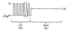
次に、図10、図11B及び図12Bを参照し、感知領域1003の例示的な動作についてここで説明する。図11Bは、上述のLCD段階及びタッチ段階中に、表示画素1003aを含む、感知領域の表示画素に対してyVcom 1016を介して印加された信号を示す。駆動領域の場合と同様に、yVcom 1016は、LCD段階中にLCD反転を行うために2.5V±2.5Vの方形波信号で駆動される。タッチ段階中、yVcom 1016は、電荷増幅器1026に接続され、これにより電圧は2.5Vの仮想接地又はその近傍に保持される。その結果として、画素電極1021も2.5Vに保持される。図10に示すように、フリンジ電界は、共通電極1023から共通電極1025に伝播する。上述のように、フリンジ電界は、駆動領域により約±2Vで変調される。表示画素1003aは、表示画素1001aと同じ又は類似の浮遊容量及びストレージキャパシタンスを有するので、これらの電界野が画素電極1021により受け取られると、信号の大部分は、共通電極1025に伝達される。 Next, an exemplary operation of the sensing region 1003 will now be described with reference to FIGS. 10, 11B and 12B. FIG. 11B shows the signals applied via
yVcom1016は、電荷増幅器1026に接続され、仮想接地に保持されているので、yVcom1016に注入された電荷により電荷増幅器の出力電圧が生成されることになる。この出力電圧は、タッチ感知システムに対してタッチ感知情報を提供する。例えば、指1027がフリンジ電界に近づくと電界の変動が発生する。この変動は、電荷増幅器1026の出力電圧の変動としてタッチシステムが検出することができる。TFT1009のドレインに接続された画素電極1021に衝突するフリンジ電界の約90%が、電荷増幅器1026に伝達されることになる。yVcom1016に直接接続された共通電極1025に衝突する電荷の100%は電荷増幅器1026に伝達されることになる。各電極に衝突する電荷比率はLCD設計に依存する。非IPSでは、パターン形成されたCFプレートが指に最も接近しているので、指により影響を受けた電荷のほぼ100%が、共通電極に衝突することができる。IPS形式ディスプレイでは、電極の各部は、指に面する面積がほぼ等しい(つまり、1/4対3/4)ので、比率は、50%前後とすることができる。一部のサブタイプのIPSディスプレイでは、画素電極は同一平面上にはなく、上向き区域の大部分が共通電極に割り当てられる。 Since
図13Aは、本開示の実施形態によるタッチスクリーンのタッチ段階中に、タッチ感知システム内で機能する領域にグループ化された多機能表示画素の別の例示的な構成を示す。図13Bは、図13Aの接地領域を有するタッチスクリーンのより詳細な図を示している。図13A〜図13Bに示すように、例えば、表示画素の領域は駆動領域と感知領域との間に形成することができ、領域は、駆動−感知接地領域1301を形成するために実際の接地に接地することができる。図13A〜図13Bはまた、2つの駆動領域間の表示画素の類似のグループを示しており、該2つの領域は、同様に接地されて駆動−駆動接地領域1303を形成することができる。接地領域及び他の領域は、例えば、導電線部分のグリッドのような接続構造体から形成することができる。例えば、図13A〜図13Bは、面/層内破断部(y−切断部)1305及び面/層内破断部(x−切断部)1309を含む水平及び垂直導電路の接地領域接続グリッド1304を示す。駆動領域をリンクする線は、面/層外バイパス1308により接地領域及び感知領域を迂回することができる。図13A〜図13Bの例示的な構成において、駆動−感知接地領域1301は、接続部1310を介し駆動−駆動接地領域1303に電気的に接続され、接地領域の全ては、タッチスクリーンの1つの境界部にてマルチプレクサ1311を介して単一接地1313に接地することができる。 FIG. 13A illustrates another exemplary configuration of multi-function display pixels grouped into regions that function within a touch sensing system during a touch screen touch phase according to embodiments of the present disclosure. FIG. 13B shows a more detailed view of a touch screen having the ground area of FIG. 13A. As shown in FIGS. 13A to 13B, for example, the region of the display pixel can be formed between the driving region and the sensing region, and the region can be in actual ground to form the driving-
図13Bは、面内破断部1305(y−切断部)及び面内破断部1309(x−切断部)を有する他の他領域からの電気的分離を維持しながら、接地領域接続グリッド1304が接続部1310を介して接地領域1301及び1303の共通電極を接続できることを示している。感知領域の共通電極は、同様にグリッドと接続することができる。図13Bはまた、駆動領域の共通電極が、駆動領域接続グリッド1321を形成するために接続部1323により接続された導電線の異なるグリッドから形成することができることを示している。駆動領域接続グリッドの水平線は、例えば、駆動領域と接地及び感知領域との間の電気的接触を防止するために、面外バイパス1308を使用して接地領域及び感知領域を延びる迂回導電路1325により接地領域及び感知領域を迂回することができる。導電路の迂回は、例えば、以下で更に詳細に説明する駆動トンネルとすることができる。図13A〜図13Bの例示的な構成においては、接地領域1301及び1303は各々、表示画素2つ分の幅であるが、接地領域の幅は、表示画素2つ分に限定されず、より少ない又はより多い数の表示画素の幅であってもよい。同様に、図13A〜図13Bは、駆動−感知接地領域に接続された駆動−駆動接地領域を示しているが、他の実施形態においては、接地領域は、他の接地領域から電気的に分離することができる。他の実施形態においては、接地領域は、AC接地などの他の形式の接地に接地することができる。接地領域1301及び1303は、駆動領域及び感知領域間及び/又は駆動領域及び駆動領域間に形成することができる静的キャパシタンスの低減を助けることができる。タッチシステム構成においてこのような静的キャパシタンスを低減すると、例えば、タッチスクリーンの精度及び電力消費量を改善させることができる。 FIG. 13B shows that the ground
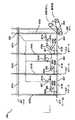
図14A〜図16Cは、第3の金属(M3)層を含む本開示の実施形態による、表示画素の多機能回路素子の別の例示的な構成を示し、更に、本開示の実施形態による表示画素を製造する例示的な方法を示している。図14A〜図16Cは、単に比較しやすいように、の3つの異なる表示画素の例示的なセットを並べて示しているが、表示画素の特定の順序付けを意味するものではない。図14A〜図14Cは、図5〜図6を参照して上記で説明した表示画素517などの駆動領域内の例示的な表示画素1401を示す。図15A〜図15Cは、図5〜図6を参照して説明した画素515のような、駆動トンネルを有する感知領域内の例示的な表示画素1501を示す。図16A〜図16Cは、駆動トンネルが無い感知領域内の例示的な表示画素1601を示す。以下の説明においては、表示画素1401、1501及び1601の全てに共通するプロセス及び構造体は、単に簡潔さを期すために単一の表示画素に関して説明している。 14A-16C illustrate another exemplary configuration of a multifunctional circuit element of a display pixel according to an embodiment of the present disclosure that includes a third metal (M3) layer, and further displays according to an embodiment of the present disclosure. 2 illustrates an exemplary method of manufacturing a pixel. 14A-16C show an exemplary set of three different display pixels side by side for ease of comparison only, but do not imply a specific ordering of display pixels. 14A-14C illustrate an
図14A、15A及び図16Aは、トランジスタの回路素子を含むポリシリコン層を形成する第1の段階を含む、処理のより早期の段階を示す。第2の段階は、全ての表示画素のM1層内のゲート線を形成する段階と、表示画素1401及び1501のM1層内のxVcom線を形成する段階とを含む。表示画素1401のxVcom線は、yVcom線との接続を可能にするために左側の延長部分を含む。xVcom線と感知領域(すなわち、バイパスがある)の他の導電路との間に接続部が形成されないので、表示画素1501のxVcom線は、感知領域内の他の導電路を迂回する駆動トンネルとしての役割を果たす。次に、表示画素のトランジスタ回路素子の上に接続部を含む接続層(CON1)が形成される。表示画素1401は、延長xVcom部上の更なる接続部を含む。データ線は、表示画素のM2層内に形成され、表示画素1401のM2層はyVcom線を含む。 14A, 15A, and 16A illustrate earlier stages of processing, including a first stage of forming a polysilicon layer that includes transistor circuit elements. The second stage includes forming a gate line in the M1 layer of all display pixels and forming an xVcom line in the M1 layer of the
図14B、15B及び図16Bは、処理の中間段階を示す。参考として、M2層も示されている。第2の接続層(CON2)は、画素電極にトランジスタのドレインを接続ために形成される。表示画素1401は、共通電極にyVcomを接続するCON2内の別の接続部を含む。次いで、共通電極が、例えばITOから形成される。 14B, 15B and 16B show an intermediate stage of processing. For reference, the M2 layer is also shown. The second connection layer (CON2) is formed to connect the drain of the transistor to the pixel electrode.
図14C、15C及び図16Cは、処理の後の段階を示しており、参考として、前の処理からのVcomを示している。第3の金属(M3)層が形成される。表示画素1401のM3層は、図示のように、表示画素1501及び1601のM3層とは異なる。感知領域表示画素1501及び1601のM3層構成部は、上下に表示画素に接続する垂直線を含み、従って、感知領域表示画素をyVcom線を使用せずにy方向に接続することが可能になる。駆動領域表示画素1401内でこのM3構造体を模擬することにより、感知領域内の更なる金属から生じる可能性があるタッチスクリーンの視覚的不適合の低減を助けることができる。第3の接続部層(CON3)が形成され、次いで、表示画素電極が全ての表示画素上に形成される。 14C, 15C and 16C show the later stages of processing, and for reference, Vcom from the previous processing is shown. A third metal (M3) layer is formed. The M3 layer of the
これらを総合すると、図14A〜図14Cは、上述の画素517に類似した駆動領域用に構成された表示画素1401を示す。表示画素1401は、第1の金属(ml)層内のゲート線1403及びxVcom線1405と、第2の金属(M2)層内のyVcom線1407及びデータ線1409とを含む。表示画素1401は、上述の接続部505のような、x−y−com接続部1411などの接続部を含むことができる。x−y−com接続部1411は、共通電極(Vcom)1413とxVcom線1405、yVcom線1407を接続する。 Taken together, FIGS. 14A-14C show a
総合すると、図15A〜図15Cは、上述の表示画素515に類似した感知領域用に構成されたタッチスクリーン表示画素1501を示す。表示画素1501は、M1層内のゲート線1503及びxVcom線1505と、M2層内のデータ線1507とを含む。xVcom線1505はスタックアップ(M1)の下位層に形成されるので、更に、xVcomとyVcomとの間に接続部が設置されないので、xVcom線は、感知領域の共通電極(Vcom)1513に接続することなく、感知領域表示画素1501を通って水平方向に「トンネル」される。これは、駆動トンネルの1つの実施例であり、当該領域を迂回しながら、すなわち迂回した領域の表示画素スタックアップ内のタッチ感知回路素子と電気的に接触せずに、感知領域などの別の形式の領域の表示画素スタックアップを延びる導電路を介して駆動領域を接続することができる。同様に、他の実施形態においては、感知領域を接続する感知トンネルなど、他の形式のトンネルを使用することができる。図15Cは、第3の金属(M3)層が、接続部グリッド1509により示すようにx及びyの両方向で感知領域内の表示画素回路素子を電気的に接続する接続部構造体として部分的に使用されることを示している。尚、yVcomが駆動画素電極1401において使用されているが、yVcomは、感知画素電極1501及び1601では使用されない。むしろ、y接続はM3層により実現される。幾つかの実施形態においては、感知領域内の表示画素は、タッチスクリーンの境界部の接続部及びスイッチを介して水平方向内に共に接続することができる。 Taken together, FIGS. 15A-15C illustrate a touch
総合すると、図16A〜図6Cは、表示画素1601が駆動トンネルを含まないことを除いては、表示画素1501と同一の表示画素1601を示す。表示画素1601は、図16Cの接続部グリッド1603で示すように、感知領域内の表示画素回路素子を電気的に接続するためにM3層内の接続部構造体を含む。 Taken together, FIGS. 16A-6C show a
図17〜図23は、第3の金属(M3)層の別の構成を含む表示画素の他の例示的な構成、表示画素を製造する例示的な方法、例示的なタッチ画素レイアウト、及び本開示の実施形態による例示的なタッチスクリーンを示す。上記の図14A〜図16Cの場合と同様に、図17〜図20は、単に比較を容易にするために、異なる製造段階における表示画素の例示的なセットの並列図を示す。図21A及び図21Bは、本開示の実施形態による、1つの例示的なタッチ画素についての表示画素の例示的なレイアウトを示す。図224及び図22−2は、図21Aに示すような例示的なタッチ画素を含むことができる例示的なタッチ画素レイアウトを示す。 17-23 illustrate other exemplary configurations of display pixels, including alternative configurations of a third metal (M3) layer, exemplary methods of manufacturing display pixels, exemplary touch pixel layouts, and books 6 illustrates an exemplary touch screen according to disclosed embodiments. As in the case of FIGS. 14A-16C above, FIGS. 17-20 show parallel views of an exemplary set of display pixels at different manufacturing stages, merely to facilitate comparison. 21A and 21B illustrate an exemplary layout of display pixels for one exemplary touch pixel according to an embodiment of the present disclosure. FIGS. 224 and 22-2 illustrate an exemplary touch pixel layout that may include an exemplary touch pixel as shown in FIG. 21A.
8つの例示的な表示画素の表示画素スタックアップ(A_pixel、B_pixel、...、H_pixelで表記される)のセットの例示的な製造プロセスである、図17〜図20を参照する。以下で更に詳細に説明するように、セット内の表示画素の各々は、以下で更に詳細に説明する3つの形式の表示画素、すなわち、接続層形式、接点形式及びトンネル形式のうちの1つである。以下の説明においては、表示画素A〜Hの全てに共通するプロセス及び構造体は、単に簡潔さを期すために、単一の表示画素について説明している場合がある。 Reference is made to FIGS. 17-20, which are exemplary manufacturing processes for a set of eight exemplary display pixel display pixel stack-ups (denoted A_pixel, B_pixel,..., H_pixel). As will be described in more detail below, each of the display pixels in the set is in one of three types of display pixels, described in more detail below: a connection layer type, a contact type and a tunnel type. is there. In the following description, the processes and structures common to all display pixels A-H may be described for a single display pixel for the sake of brevity.
図17は、トランジスタ1701の回路素子を含む、ポリシリコン層を形成する第1の段階を含む例示的な処理のより早期の段階を示す。第2の段階は、全ての表示画素のM1層内のゲート線を形成する段階と、表示画素E〜HのM1層内のxVcom線1705を形成する段階とを含む。表示画素E〜FのxVcom線は、共通電極への接続を可能にするために、中間サブ画素において延長部分1706を含む。xVcom線と感知領域(すなわち、バイパスがある)の他の導電路との間に接続部が形成されないので、表示画素G−HのxVcom線は、感知領域内の他の導電路を迂回する駆動トンネルとしての役割を果たす。次に、表示画素のトランジスタ回路素子上、更に、延長xVcom部1706上に接続部を含む接続層(CON1)が形成される。データ線1709が表示画素のM2層内に形成される。 FIG. 17 illustrates an earlier stage of an exemplary process that includes a first stage of forming a polysilicon layer, including the circuit elements of
図18は、例示的な処理の中間段階を示す。参考として、M2層も示されている。第2の接続層(CON2)は、接続部1801により共通電極(Vcom)1805にトランジスタのドレインを接続するために形成される。表示画素E〜Fは、共通電極1805にxVcom 1705を接続する、CON2内の別の接続部1803を含む。次に、共通電極1805は、例えば、ITOなどの実質的に透明導体から形成することができる。 FIG. 18 illustrates an intermediate stage of the exemplary process. For reference, the M2 layer is also shown. The second connection layer (CON2) is formed in order to connect the drain of the transistor to the common electrode (Vcom) 1805 through the
図19は、例示的な処理の後の段階を示しており、参考として、前の処理からのVcom1805を示している。図19に示す処理においては、第3の金属(M3)層及び第3の接続部層(CON3)が形成される。CON3層1905は、表示画素電極に接続する。M3層は、Vcom 1805と電気的に接触して形成される。各表示画素のM3層は、2つの垂直線1901及び1つの水平線1903を含む。幾つかの実施形態においては、M3層は、他の実施形態のyVcom線と同じ目的を提供することができる。一般に、幾つかの実施形態においては、M3層は、M3層自体とデータ/ゲート線との間の相対的に低いクロスキャパシタンスを実現することができる点で一定の利点を有することができる。更に、感知領域においては、M3層の水平(x方向)接続部は、y方向電荷感知を向上させるために、全ての感知共通電極を共に結合する役割を果たすことができる。感知領域内の共通電極のx−y接続部は、均一性が得られるように、駆動領域内で繰り返すことができる。更にまた、データ線上に垂直M3線(y方向)を位置決めすることにより、開口率の向上を達成することができる。感知領域を迂回するために、M3層に対しても駆動トンネルを使用することができるので、M3層の水平(x方向)接続部は、駆動トンネルを覆って、及び開口率を増大させるように位置合わせされた任意のxVcom層を覆って配置することができる。xVcom線が使用されない画素の実施形態においては、誘導用駆動線信号をM3層に供給することができる。一般的には、シミュレーション駆動線信号を、xVcom線及びM3層の一方又は両方に供給することができる。各表示画素内の垂直線1901は、セットの特定の表示画素(すなわち、A_pixel、B_pixel、その他)に応じて、y切断部又はy接続部を含むことができる。図19において、B_pixelのy−接続部及びC_pixelのy切断部は強調表示されている。各表示画素内の水平線1903は、セットの特定の表示画素に応じてx−切断部又はx−接続部を含むことができる。図19において、A_pixelのx−接続部及びE_pixelのx−切断部は、強調表示されている。表示画素A、F及びHのM3層の垂直線1901及び水平線1903は、表示画素の縁部(上、下、左、右)まで延在し、場合によっては、各方向で隣接する表示画素に表示画素A、F及びHを接続することができる。従って、表示画素A、F及びHは、x−接続部及びy−接続部(x−con、y−con)を提供する。各表示画素の水平線1903が左右の隣接する表示画素間に導電路を形成し、各表示画素の垂直線1901が上下の隣接する表示画素間で導電路を形成するので、表示画素A、F及びHは、x接続及びy接続表示画素として表記される。しかしながら、表示画素A、F及びHはx方向及びy方向の両方において接続する接続構造体を有するが、隣接する表示画素の1つ又はそれ以上は、例えば、画素A、F又はHから隣接する表示画素を切断する切断部をM3層において含むことができるので、表示画素は、必ずしも隣接する表示画素に接続されるわけではない。 FIG. 19 shows a later stage of an exemplary process, and for reference, shows
表示画素B、E及びGの各々におけるM3層は、垂直方向に完全に延在するが、表示画素の右縁部までは延在しない。これらの表示画素は、x−切断部及びy接続部(x−discon、y−con)を提供する。更に詳細には、表示画素B、E及びGは「右側で切断され」、すなわち、右側では表示画素のM3層に接続していない。同様に、表示画素CのM3層は、x−接続部及びy切断部(x−con、y−discon)を提供し、更に詳細には、画素Cは「下側で切断されている」。表示画素DのM3層は、x−切断部及びy切断部(x−discon、y−discon)を提供し、更に詳細には、画素Dは、「右側及び下側で切断されている」。切断部は、右側及び/又は下側に限定されず、上側、左側、或いは、表示画素のM3層の内部に、あらゆる数及び組み合わせで存在することができる点に留意されたい。 The M3 layer in each of the display pixels B, E, and G extends completely in the vertical direction, but does not extend to the right edge of the display pixel. These display pixels provide an x-cut and a y-connect (x-discon, y-con). More specifically, the display pixels B, E and G are “cut off on the right side”, that is, not connected to the M3 layer of the display pixel on the right side. Similarly, the M3 layer of the display pixel C provides an x-connection and a y-cut (x-con, y-discon), and more specifically, the pixel C is “cut off on the lower side”. The M3 layer of the display pixel D provides an x-cut and a y-cut (x-discon, y-discon), and more specifically, the pixel D is “cut on the right and bottom sides”. It should be noted that the cuts are not limited to the right side and / or the lower side, but may be present in any number and combination on the upper side, the left side, or within the M3 layer of the display pixel.
図20は、例示的な処理の更に後の段階を示す。M3層及びCON3層は、参照として示されている。表示画素電極2001及びブラックマスク(BM)2003が全ての表示画素上に形成される。図17〜図20では、図5の実施形態において存在したyVcom線接続が存在しない。むしろ、M3層は、x方向及びy方向で共通電極を接続する目的を果たすことができる。しかしながら、xVcomは、駆動トンネル、すなわち感知領域バイパスを提供するために、依然として、幾つかの画素(すなわち、E、F、G、H)において使用することができる。 FIG. 20 shows a further stage in the exemplary process. The M3 and CON3 layers are shown as references. A
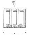
図21及び図21Bは、1つの例示的なタッチ画素に関する表示画素の例示的なレイアウトを示す。タッチ画素2103は、64x64表示画素の領域を含み、表示画素の各々は、図に示す表示画素の凡例に従って上述した表示画素A〜Hのうちの1つである。図21Aはまた、150個(15x10)タッチ画素2103の例示的な構成を含む例示的なタッチスクリーン2101を示す。表示画素レイアウトは、図4及び図13を参照して上述した駆動領域セグメント、感知領域及び接地領域に実質的に対応することができる表示画素のグループを作成する。特に、表示画素のレイアウトは、2つのX領域(X1及びX2)、2つのY領域(Y1及びY2)及び1つのZ領域を形成する。X1領域及びX2領域は、例えば、図3では、それぞれ、右半部分309及び左半部分313など、駆動領域セグメントの右半部分及び別の駆動領域セグメントの左半部分とすることができる。Y領域は、例えば、図13の駆動−感知接地領域1301などの接地領域の一部とすることができる。Z領域は、例えば、図3の感知線223などの感知領域の一部とすることができる。図17から図20に示す8つの表示画素のセットの特定の構成は、図21A及び図21Bに示す特定の設計画素レイアウトと共に、タッチを検出するためにタッチ感知システムにおいて使用することができる回路素子のグループを作成する。 21 and 21B show an exemplary layout of display pixels for one exemplary touch pixel. The touch pixel 2103 includes an area of 64 × 64 display pixels, and each display pixel is one of the display pixels A to H described above according to the legend of the display pixels shown in the figure. FIG. 21A also shows an
図17〜20及び図21Aの凡例に照らすとわかるように、縦列1〜23からの表示画素及び横列1〜64からの表示画素が共にM3層において接続され、駆動領域X1を形成する。接地領域Y1は、縦列24〜25及び横列1〜64の表示画素を含む。感知領域Zは、縦列26〜39、及び横列1〜64を含む。接地領域Y2は、縦列40〜41及び横列1〜64の表示画素を含む。駆動領域X2は、縦列42〜64、及び横列1〜64を含む。 As can be seen in the legend of FIGS. 17-20 and 21A, the display pixels from columns 1-23 and the display pixels from rows 1-64 are both connected in the M3 layer to form the drive region X1. The ground region Y1 includes display pixels in
駆動領域X1及びX2は、駆動トンネル(バイパス)2105の表示画素の回路素子を介して共に電気的に接続されている。駆動トンネル2105は、表示画素E、H、G及びFを含む。図20を参照すると、表示画素E及びFは、図でわかるように、M1層内のxVcomと接続するための導電層Vcom ITO、CON2、M2及びCON1を介してM3層(図20の接点2005にて)間で「接点」を提供する。従って、表示画素E及びFにより、駆動領域のM3は、トンネリング(xVcom(M1)層への層外/面外バイパスを作成)により接地領域及び感知領域を迂回することが可能になる。 The drive regions X 1 and
表示画素G及びHは、回路素子xVcomを含み、xVcomと、以下で更に詳細に説明するタッチ感知システム内で動作する表示画素の他の回路素子の何れかとの間に接続部を含まない。従って、表示画素形式G及びHは、2つの駆動領域、例えば、駆動領域X1及びX2を共に接続するために、接地領域及び感知領域を迂回するトンネリング接続部の実施例である。 Display pixels G and H include circuit element xVcom and do not include a connection between xVcom and any of the other circuit elements of the display pixel operating in the touch sensing system described in more detail below. Accordingly, display pixel types G and H are examples of tunneling connections that bypass the ground and sensing areas to connect two drive areas, eg, drive areas X1 and X2, together.
図17〜図20を再び参照し、ここで、表示画素、接続層形式、接点形式及びトンネル形式の3つの例示的な形式について、図21A及び図21Bの例示的な表示画素レイアウトに対して更に詳細に説明する。この実施例においては、各領域内の表示画素の共通電極は、主として本明細書では接続層と呼ばれるM3層を介して共に接続される。A_pixel、B_pixel、C_pixel及びD_pixelは、接続層を介して表示画素の共通電極を共に接続する共通機能を提供することができる、接続層形式の表示画素である。詳細には、上述のように、垂直線1901及び水平線1903は、表示画素の共通電極に電気的に接続される。接続層形式の表示画素の4つの異なるM3層構成により、表示画素間にM3層を接続する4つの異なる方法が得られる。A_pixelは、全ての隣接する表示画素(上、下、左、及び右)においてM3層を接続することができる。B_pixelは、上、下、及び左側に接続することができるが、右側に表示画素からの切断部を設けている。C_pixelは、上、下、右側に接続することができるが、下側に表示画素からの切断部を設けている。D_pixelsは、上及び左側に接続することができるが、右側及び下側に表示画素からの切断部を設けている。図21Aを参照すると、表示画素レイアウトの表示画素の大半は、A_pixelとすることができ、A_pixelは通常、全ての隣接画素を効率的に接続するように領域の内部区域内に位置付けることができる。 Reference is again made to FIGS. 17-20, where three exemplary formats of display pixel, connection layer type, contact type and tunnel type are further illustrated with respect to the exemplary display pixel layout of FIGS. 21A and 21B. This will be described in detail. In this embodiment, the common electrodes of the display pixels in each region are connected together mainly through an M3 layer called a connection layer in this specification. A_pixel, B_pixel, C_pixel, and D_pixel are connection layer type display pixels that can provide a common function of connecting together the common electrodes of the display pixels through the connection layer. Specifically, as described above, the
B_pixel、C_pixel及びD_pixelは、これらの表示画素のx切断部及びy切断部が、領域の境界を形成する切断部を提供することができるので、領域の境界に位置付けることができる。例えば、右側で切断されているB_pixelは、図21Aに示すように垂直線内に配設され、左側及び右側で領域を分離することができる。C_pixelは、図21Aに示すように、水平線内に配設され、上側及び下側で領域を分離することができる。D_pixelは、領域のコーナ内に配置され、左右及び上下側で領域を分離することができる。 B_pixel, C_pixel, and D_pixel can be positioned at the boundary of the region because the x-cutting portion and the y-cutting portion of these display pixels can provide a cutting portion that forms the boundary of the region. For example, B_pixel cut on the right side is arranged in a vertical line as shown in FIG. 21A, and the region can be separated on the left side and the right side. As shown in FIG. 21A, C_pixel is disposed within a horizontal line, and can divide a region on the upper side and the lower side. D_pixel is arranged in the corner of the region, and can separate the region on the left, right, and upper and lower sides.
画素A〜Dだけを使用して、図21Aに示す駆動領域セグメント、感知線及び接地領域を形成することが可能である。しかしながら、本発明の幾つかの実施形態においては、駆動領域セグメントは、接地領域及び感知領域などの他の領域を迂回する導電路を介して共に電気的に接続される。接点形式表示画素、すなわち、E_pixel及びF_pixel、並びにトンネル形式表示画素、すなわち、C_pixel及びH_pixelは、他の領域を迂回する導電路を形成することができる。接点形式画素は、表示画素のスタックアップ内の2つ又はそれ以上の導電層を電気的に接続又は切断することができる。本明細書で説明する例示的な接点形式表示画素は、第1の金属層(M1層)内に形成することができる接続部をM3層とxVcom線との間に含む。従って、接点形式画素は、異なる導電路、すなわちM1層内のxVcom線に駆動領域セグメントの接続層(M3層)を接続することにより、面/層外バイパスを形成する。トンネル形式表示画素は、xVcom線を含むが、M3層などの接続部をxVcom線と表示画素スタックアップの他の何れかの回路素子との間に含まない。 Only the pixels A to D can be used to form the drive region segment, sense line, and ground region shown in FIG. 21A. However, in some embodiments of the present invention, the drive region segments are electrically connected together via conductive paths that bypass other regions such as the ground region and the sensing region. The contact type display pixels, ie, E_pixel and F_pixel, and the tunnel type display pixels, ie, C_pixel and H_pixel, can form conductive paths that bypass other regions. A contact-type pixel can electrically connect or disconnect two or more conductive layers in a display pixel stackup. The exemplary contact-type display pixel described herein includes a connection between the M3 layer and the xVcom line that can be formed in the first metal layer (M1 layer). Thus, the contact-type pixels form a surface / outside layer bypass by connecting the connection layer (M3 layer) of the drive region segment to a different conductive path, i.e., xVcom line in the M1 layer. The tunnel type display pixel includes an xVcom line, but does not include a connection portion such as an M3 layer between the xVcom line and any other circuit element in the display pixel stackup.
ここで、迂回導電路を更に詳細に説明する。図21A及び図21Bに示すように、タッチ画素2103は3つの駆動トンネル2105を含む。各駆動トンネル2105は、画素形式の以下のパターン内の表示画素、すなわち、E、H、G、H...H、G、H、G、Fを含む。駆動トンネル2105は、迂回導電路の1つの実施例である。駆動トンネル2105の左端から始めて、迂回導電路は、E_pixelで始まり、E_pixelは、図21において駆動領域セグメントと接地領域との間で接続層を切断する右切断部を接続層内に含む。結果として、E_pixelの右切断部により、2つの駆動領域セグメント間の接続層内の+x切断部が生じ、E_pixelの面/層外接続部により、2つの駆動領域セグメント間の別の層(M1)内のx接続部が生じる。 Here, the bypass conductive path will be described in more detail. As shown in FIGS. 21A and 21B, the touch pixel 2103 includes three drive tunnels 2105. Each drive tunnel 2105 is a display pixel in the following pattern in pixel format: E, H, G, H.P. . . H, G, H, G, F are included. The drive tunnel 2105 is one example of a bypass conductive path. Starting from the left end of the drive tunnel 2105, the bypass conductive path starts with E_pixel, and the E_pixel includes a right cut portion in the connection layer that cuts the connection layer between the drive region segment and the ground region in FIG. As a result, the right cut of E_pixel results in a + x cut in the connection layer between the two drive region segments, and another layer (M1) between the two drive region segments due to the E_pixel face / out-layer connection. The x connection inside is produced.
他の層に対する面/層外接続部が作製されると、迂回導電路は、トンネル形式表示画素を使用して他の領域、すなわち接地領域及び感知領域を延びる。トンネル形式表示画素は各々、xVcom線を含み、或いは、x切断部及びx接続部を含む。更に詳細には、G_pixelは右切断部を含み、H_pixelは右接続部を含む。トンネル形式表示画素のx接続/切断は、例えば、2つ以上の他の領域を2つの駆動領域セグメント間に形成可能にすることができる。特に、図21に示すように、G_pixelは、E_pixelの垂直縦列内に形成され、接地領域Y1と感知領域Zと間の境界、感知領域Zと接地領域Y2との間の境界、及び接地領域Y2と駆動領域セグメントX2との間の境界を形成するように切断部を作成することができる。H_pixelの接続層(M3層)が、A_pixelと同様に全ての隣接画素に接続されるので、H_pixelは、接地領域及び感知領域などの他の領域の内部区域内に位置付けることができる。 When surface / outside layer connections to other layers are made, the bypass conductive path extends to other regions, ie, the ground and sensing regions, using tunnel type display pixels. Each tunnel-type display pixel includes an xVcom line, or includes an x-cut portion and an x-connection portion. More specifically, G_pixel includes a right cut portion, and H_pixel includes a right connection portion. The x-connection / disconnection of the tunnel-type display pixel can, for example, allow two or more other regions to be formed between two drive region segments. In particular, as shown in FIG. 21, G_pixel is formed in a vertical column of E_pixels, and includes a boundary between the ground area Y1 and the sensing area Z, a boundary between the sensing area Z and the ground area Y2, and a ground area Y2. And the drive region segment X2 can be cut. Since the connection layer (M3 layer) of H_pixel is connected to all adjacent pixels in the same way as A_pixel, H_pixel can be positioned in the internal area of other regions such as the ground region and the sensing region.
図22−1及び図22−2は、本開示の実施形態による、例示的なタッチ画素レイアウト及びタッチスクリーン2201を示す。タッチスクリーン2201は、LCD回路(図示せず)にタッチスクリーン2201を接続するLCD FPC(フレキシブルプリント基板)、表示段階において表示画素を駆動するLCD駆動装置、タッチスクリーン用共通電圧を流すVcom線を含む。タッチFPCは、以下の線、すなわち、駆動領域に駆動信号を送信するr0−r14及びr14−r0線、感知領域から感知信号を受信するc0−c9線、並びに、タッチスイッチ(TSW)に接続するtswX線、tswY線、及びtswZ線(本明細書では「tswX、Y、Z」と呼ばれる場合がある)を含み、これらtswX線、tswY線、及びtswZ線は、タッチ段階における全てのデータ線の仮想接地接続から表示段階中のLCD駆動装置による対応するデータ出力に対するそれぞれのデータ線の接続へのスイッチング、タッチ感知段階中の感知領域間のスイッチング、その他など、種々のスイッチングを制御することができる。タッチFPCはまた、仮想接地にデータ線及び接地領域をそれぞれ接続する、g1線及びg0線を含む。ゲート線を駆動するゲートドライバが含まれる。 22-1 and 22-2 illustrate an exemplary touch pixel layout and touch screen 2201, according to embodiments of the present disclosure. The touch screen 2201 includes an LCD FPC (flexible printed circuit board) that connects the touch screen 2201 to an LCD circuit (not shown), an LCD driving device that drives display pixels in a display stage, and a Vcom line that supplies a common voltage for the touch screen. . The touch FPC is connected to the following lines: r0-r14 and r14-r0 lines that transmit a driving signal to the driving area, c0-c9 lines that receive a sensing signal from the sensing area, and a touch switch (TSW). including tswX line, tswY line, and tswZ line (sometimes referred to herein as “tswX, Y, Z”), and these tswX line, tswY line, and tswZ line are all of the data lines in the touch stage. Various switching can be controlled, such as switching from virtual ground connection to the connection of each data line for the corresponding data output by the LCD driver during the display phase, switching between sensing areas during the touch sensing phase, etc. . The touch FPC also includes a g1 line and a g0 line that connect the data line and the ground region to the virtual ground, respectively. A gate driver for driving the gate line is included.
図22−2はまた、タッチスクリーン2201の側面図を示す。側面図は、接続部の一部を更に詳細に示している。例えば、図22−2は、Y領域からのM3接続部により、Y領域をg0に接地することができることを示している。Z領域からのM3接続部により、Z領域を共同c9線に接続することができる。M2接続部により、データ線をタッチ感知段階中にglに接地することができる。 FIG. 22-2 also shows a side view of the touch screen 2201. The side view shows a part of the connection part in more detail. For example, FIG. 22-2 shows that the Y region can be grounded to g0 by the M3 connection from the Y region. The Z region can be connected to the common c9 line by the M3 connection from the Z region. The M2 connection allows the data line to be grounded to gl during the touch sensing phase.
図23は、本開示の実施形態による、高抵抗(R)遮蔽体を含む例示的なタッチスクリーンの側面図である。図23は、カバー2301、接着材2302、偏光板2303、高抵抗(R)遮蔽体2304、カラーフィルタガラス2305、駆動領域2309、感知領域2313、接地領域2315、TFTガラス2316、及び第2の偏光板2317を含む、タッチスクリーン2300の一部を示す。液晶層は、カラーフィルタガラスの下方に配置することができる。高R遮蔽体2304などの高抵抗遮蔽体は、例えば、FFS LCD用低抵抗率遮蔽層の代わりに、CFガラスと前方偏光板との間に設置することができる。高R遮蔽体のシート抵抗は、例えば、200Mオーム/スクエア〜2Gオーム/スクエアとすることができる。幾つかの実施形態においては、高電気抵抗率遮蔽膜を有する偏光板は、高R遮蔽層として使用することができ、従って、例えば、偏光板2303及び高R遮蔽体2304は単一の高R遮蔽偏光板に置き換えられる。高R遮蔽体は、ディスプレイ近傍の低周波/DC電圧によるディスプレイ動作の妨害を阻止するのを助けることができる。同時に、高R遮蔽体は、容量性タッチ感知に通常使用されるものなどの高周波信号が遮蔽体を貫通できるようにすることができる。従って、高R遮蔽体は、ディスプレイの遮蔽を助けると共に、ディスプレイがタッチ事象を感知可能にすることができる。高R遮蔽体は、例えば、超高抵抗有機物質、カーボンナノチューブ、その他から作ることができる。 FIG. 23 is a side view of an exemplary touch screen including a high resistance (R) shield according to an embodiment of the present disclosure. 23 shows a
図24は、本開示の実施形態による、別の例示的な容量式一体型タッチスクリーン2400の部分平面図である。この特定のタッチスクリーン2400は、自己キャパシタンスベースであり、従って、各々がタッチスクリーン2400の平面内の異なる座標を表す、複数のタッチ感知領域2402を含む。タッチ画素2402は、タッチスクリーン2400上で画像を表示する表示回路の一部として、及びタッチスクリーン上又はその近傍でタッチを感知するタッチ感知回路の一部として動作する多機能回路素子を含む表示画素2404から形成される。この例示的な実施形態においては、タッチ感知回路及びシステムは、自己キャパシタンス、従って、タッチ画素2402内の回路素子の自己キャパシタンスに基づいて動作する。幾つかの実施形態においては、自己キャパシタンス及び相互キャパシタンスの組み合わせを用いて、タッチを感知することができる。 FIG. 24 is a partial plan view of another exemplary capacitive
本開示の実施形態を添付図面を参照しながら十分に説明してきたが、限定ではないが、異なる実施形態の特徴の組み合わせ、1つ又は複数の特徴の省略、その他を含む、様々な変更及び改変は、本明細書及び各図に照らして当業者には明らかとなる点に留意されたい。 While embodiments of the present disclosure have been fully described with reference to the accompanying drawings, various changes and modifications may be made including, but not limited to, combinations of features of different embodiments, omission of one or more features, etc. Note that this will be apparent to those skilled in the art in light of this specification and the figures.
例えば、上述のコンピュータシステム200の機能の1つ又はそれ以上は、メモリ(例えば図2の周辺機器204の1つ)内に格納されたファームウェアにより実施されて、タッチプロセッサ202により実行するか、或いは、プログラムストレージ232内に格納して、ホストプロセッサ228により実行することができる。ファームウェアはまた、コンピュータベースのシステム、プロセッサ組み込みシステム、或いは、命令実行システム、装置又はデバイスから命令をフェッチして該命令を実行することができる他のシステムといった、命令実行システム、装置又はデバイスが使用するため又はこれらに関連して任意のコンピュータ可読媒体に格納及び/又は移送することができる。この実施形態の状況においては、「コンピュータ可読媒体」は、命令実行システム、装置具又はデバイスが使用するため又はこれらに関連してプログラムを含む又は格納することができる任意の媒体とすることができる。コンピュータ可読媒体は、限定ではないが、電子、磁気、光学、電磁、赤外線又は半導体システム、装置、又はデバイス、ポータブルコンピュータディスケット(磁気)、ランダムアクセスメモリ(RAM)(磁気)、読み取り専用メモリ(ROM)(磁気)、消去及びプログラム可能読取り専用メモリ(BPROM)(磁気)、又は、CD、CD−R、CD−RW、DVD、DVD−R又はDVD−RWなどの携帯型光ディスク、或いは、コンパクトフラッシュ(登録商標)カード、セキュアデジタルカード、USBメモリデバイス、メモリースティック、及び同様のものなどのフラッシュメモリなどを含むことができる。 For example, one or more of the functions of
ファームウェアはまた、コンピュータベースのシステム、プロセッサ組み込みシステム、或いは、命令実行システム、装置又はデバイスから命令をフェッチして該命令を実行することができる他のシステムといった、命令実行システム、装置又はデバイスが使用するため又はこれらに関連して任意の移送媒体内で伝播することができる。この実施形態の状況においては、「移送媒体」は、命令実行システム、装置具又はデバイスが使用するため又はこれらに関連してプログラムを伝達、伝播、又は移送することができる任意の媒体とすることができる。移送可読媒体は、限定ではないが、電子、磁気、光学、電磁、又は赤外線有線又は無線の伝播媒体を含むことができる。 Firmware is also used by instruction execution systems, devices, or devices, such as computer-based systems, processor-embedded systems, or other systems that can fetch and execute instructions from an instruction execution system, device, or device Can be propagated in or in any transport medium. In the context of this embodiment, the “transport medium” is any medium that can transmit, propagate, or transport a program for use in connection with or in connection with an instruction execution system, apparatus, or device. Can do. Transport readable media can include, but is not limited to, electronic, magnetic, optical, electromagnetic, or infrared wired or wireless propagation media.
更なる好適な実施形態を以下のように説明することができる。 Further preferred embodiments can be described as follows.
複数の表示画素のスタックアップは、ゲート線を含む導電性材料の第1の層と、データ線を含む導電性材料の第2の層と、第1の方向の第1の導電線を含む導電性材料の第3の層とを有する。第1の導電線の各々は、複数の表示画素を介して延在し、第3の層内の切断部により第1の方向に互いに分離された複数の第1の線部分を含む。第1の方向を横断する第2の方向に配置された第2の導電線も設けられる。第2の導電線の各々は、複数の表示画素を介して延在し、切断部により第2の方向に互いに分離された複数の第2の線部分を含む。第1の領域内の表示画素の回路素子は、第1の複数の第1の線部分により第1の方向に共に電気的に接続され、第1の領域内の表示画素の回路素子は、第1の複数の第2の線部分により第2の方向に共に電気的に接続される。スタックアップの第3の層は、第2の導電線を含むことができ、第2の線部分の切断部は、第3の層に存在することができる。表示画素の第2の領域も設けることができ、該第2の領域の表示画素の回路素子は、第2の複数の第1の線部分及び第2の複数の第2の線部分それぞれによって、第1及び第2の方向に共に電気的に接続され、第3の層内で第1の領域内の回路素子から電気的に切断される。回路素子は、表示画素の共通電極とすることができる。スタックアップは、表示画素の第3の領域を含むことができ、該第3の領域の表示画素の回路素子は、第3の複数の第1の線部分及び第3の複数の第2の線部分によって、第1及び第2の方向に共に電気的に接続され、第3の領域は、第1及び第2の領域の間に位置付けられ、少なくとも1つの導電路は、第1の領域の回路素子を第2の領域の回路素子に接続し、少なくとも1つの導電路は、第3の領域の回路素子に電気的に接続することなく、第3の領域の1つ又はそれ以上の表示画素を延びる。スタックアップの導電路は、第1の層内の共通線と、第1の領域の回路素子の少なくとも一部を共通線に電気的に接続する第1の導電接点と、第2の領域の回路素子の少なくとも一部を共通線に電気的に接続する第2の導電接点とを含むことができる。 The plurality of display pixel stackups includes a first layer of conductive material including a gate line, a second layer of conductive material including a data line, and a conductive layer including a first conductive line in a first direction. A third layer of a conductive material. Each of the first conductive lines includes a plurality of first line portions that extend through the plurality of display pixels and are separated from each other in the first direction by a cut portion in the third layer. A second conductive line is also provided that is disposed in a second direction that intersects the first direction. Each of the second conductive lines includes a plurality of second line portions that extend through the plurality of display pixels and are separated from each other in the second direction by the cutting portion. The circuit elements of the display pixels in the first region are electrically connected together in the first direction by the first plurality of first line portions, and the circuit elements of the display pixels in the first region are The plurality of second line portions are electrically connected together in the second direction. The third layer of the stack-up can include a second conductive line, and a cut in the second line portion can be present in the third layer. A second region of the display pixel can also be provided, and the circuit elements of the display pixel in the second region are respectively provided by the second plurality of first line portions and the second plurality of second line portions. Electrically connected together in the first and second directions and electrically disconnected from the circuit elements in the first region within the third layer. The circuit element can be a common electrode of the display pixel. The stack-up can include a third region of display pixels, and the circuit elements of the display pixels in the third region include a third plurality of first line portions and a third plurality of second lines. The portion is electrically connected together in the first and second directions, the third region is positioned between the first and second regions, and the at least one conductive path is a circuit of the first region. Connecting the element to a circuit element in the second region, wherein at least one conductive path electrically connects one or more display pixels in the third region without electrically connecting to the circuit element in the third region. Extend. The stack-up conductive path includes a common line in the first layer, a first conductive contact that electrically connects at least part of the circuit elements in the first region to the common line, and a circuit in the second region. A second conductive contact electrically connecting at least a portion of the element to the common line.
また、第1の領域と第2の領域との間に位置付けられる表示画素の第4の領域を設けることができ、導電路の少なくとも一部は、第4の領域の回路素子に電気的に接続することなく、第4の領域の1つ又はそれ以上の表示画素を延びる。また、他の実施形態においては、第4の領域を接地に接続する導電線を設けることもできる。 Further, a fourth region of the display pixel positioned between the first region and the second region can be provided, and at least a part of the conductive path is electrically connected to the circuit element in the fourth region. Without extending one or more display pixels of the fourth region. In other embodiments, a conductive line connecting the fourth region to ground can also be provided.
タッチ感知システムはまた、第1及び第2の領域の一方に接続された駆動信号発生器と、第3の領域に接続された感知チャンネルとを含むことができる。 The touch sensing system can also include a drive signal generator connected to one of the first and second regions and a sensing channel connected to the third region.
各表示画素は、別個の共通電極を有し、第1の複数の第1の線部分及び第1の複数の第2の線部分は、第1の領域内の表示画素の共通電極を共に接続する。第2の複数の第1の線部分及び第2の複数の第2の線部分は、第2の領域の表示画素の共通電極を共に接続する。第3の複数の第1の線部分及び第3の複数の第2の線部分は、第3の領域の表示画素の共通電極を共に接続する。駆動信号発生器は、第1の領域内の第1の複数の第1の線部分又は第1の複数の第2の線部分の少なくとも一方に、或いは、第2の領域内の第2の複数の第1の線部分又は第2の複数の第2の線部分の少なくとも一方に接続される。感知チャンネルは、第3の複数の第1の線部分又は第3の複数の第2の線部分の一方に接続することができ、該感知チャンネルは電荷増幅器を含むことができる。 Each display pixel has a separate common electrode, and the first plurality of first line portions and the first plurality of second line portions are connected together with the common electrodes of the display pixels in the first region. To do. The second plurality of first line portions and the second plurality of second line portions connect together the common electrodes of the display pixels in the second region. The third plurality of first line portions and the third plurality of second line portions connect together the common electrodes of the display pixels in the third region. The drive signal generator is provided on at least one of the first plurality of first line portions or the first plurality of second line portions in the first region, or the second plurality of first line portions in the second region. Are connected to at least one of the first line portion or the second plurality of second line portions. The sense channel can be connected to one of the third plurality of first line portions or the third plurality of second line portions, and the sense channel can include a charge amplifier.
タッチスクリーンは、表示画素の第1の回路素子及びディスプレイドライバに対する接続部を含む表示回路と、タッチ感知回路とを含み、該タッチ感知回路は、表示画素の第1の回路素子の一部を有する第1の導電線と、表示画素の第2の異なる回路素子を有する少なくとも1つの導電路によって共に電気的に接続された少なくとも2つの導電線部分を含む第2の導電線とを備える。第1及び第2の導電線の一方は、タッチ感知回路の駆動線であり、第1及び第2の導電線の他方は、タッチ感知回路の感知線である。更にまた、少なくとも2つの導電線部分は第1の回路素子の少なくとも一部を含むことができ、第1の回路素子は、表示画素の共通電極を含むことができ、第2の回路素子は、共通電圧線を含むことができる。また、実質的に第1及び第2の導電線の2つの導電線の間に導電領域を設けることができ、該導電領域は接地される。更にまた、導電領域は交流(AC)接地に接地されてもよい。 The touch screen includes a display circuit including a connection portion with respect to the first circuit element of the display pixel and the display driver, and a touch sensing circuit, and the touch sensing circuit includes a part of the first circuit element of the display pixel. A first conductive line and a second conductive line including at least two conductive line portions electrically connected together by at least one conductive path having a second different circuit element of the display pixel. One of the first and second conductive lines is a drive line of the touch sensing circuit, and the other of the first and second conductive lines is a sensing line of the touch sensing circuit. Still further, the at least two conductive line portions can include at least a portion of the first circuit element, the first circuit element can include a common electrode of the display pixel, and the second circuit element includes: A common voltage line can be included. Further, a conductive region can be provided between the two conductive lines of the first and second conductive lines, and the conductive region is grounded. Furthermore, the conductive region may be grounded to an alternating current (AC) ground.
更に別の実施形態は、プロセッサと、メモリと、表示画素の複数の回路素子を含む表示回路及び表示制御装置を含むディスプレイシステムと、タッチ感知システムとを備えるコンピュータシステムとして説明することができる。タッチ感知システムは、複数の第1の領域及び複数の第2の領域にグループ化された複数の回路素子を有するタッチ感知回路を含むことができ、第2の領域を通る導電路は、第2の領域を迂回しながら複数の第1の領域を接続する。第1の領域の各々の回路素子は、第1の方向に沿って、及び第1の方向を横断する第2の方向に沿って共に電気的に接続することができ、また、タッチ制御装置を設けることもできる。更にまた、第2の領域の各々の回路素子は、第1及び第2の方向の一方に沿って共に電気的に接続することができる。 Yet another embodiment can be described as a computer system comprising a processor, a memory, a display system including a display circuit and a display controller including a plurality of circuit elements of display pixels, and a touch sensing system. The touch sensing system can include a touch sensing circuit having a plurality of circuit elements grouped into a plurality of first regions and a plurality of second regions, the conductive path through the second region being a second region. A plurality of first areas are connected while bypassing the area. Each circuit element in the first region may be electrically connected together along a first direction and along a second direction that intersects the first direction, and the touch control device may It can also be provided. Furthermore, each circuit element in the second region can be electrically connected together along one of the first and second directions.
更なる好ましい実施形態は、一体型ディスプレイを有するタッチスクリーンとして説明することができる。タッチスクリーンは、各々が対応する回路素子を有する複数の表示画素と、各々が表示画素の少なくとも第1の複数の回路素子を含む複数の駆動線と、駆動線を横断して配置され、表示画素の少なくとも第2の複数の回路素子を含む複数の感知線と、複数の駆動線及び複数の感知線の隣接画素により形成された複数のタッチ画素とを備える。複数の表示画素は、第1の画素形式を含み、第1の画素形式は、該第1の画素形式の対応する回路素子に接続され、且つ正及び負の第1の方向並びに正及び負の第2の方向の両方に沿った少なくとも隣接する第1の画素形式に電気的に接続された第1の導電層を含む。タッチスクリーンのディスプレイは、液晶ディスプレイとすることができる。タッチスクリーンは更に、複数の表示画素に接続された複数のゲート線と、複数の表示画素に接続された複数のデータ線とを含むことができる。更にまた、複数の表示画素の各々の対応する回路素子は、液晶ディスプレイの共通電極を含むことができる。 A further preferred embodiment can be described as a touch screen with an integrated display. The touch screen includes a plurality of display pixels each having a corresponding circuit element, a plurality of drive lines each including at least a first plurality of circuit elements of the display pixels, and arranged across the drive lines. A plurality of sensing lines including at least a second plurality of circuit elements, and a plurality of touch pixels formed by a plurality of drive lines and pixels adjacent to the plurality of sensing lines. The plurality of display pixels includes a first pixel format, the first pixel format is connected to a corresponding circuit element of the first pixel format, and has a positive and negative first direction and positive and negative A first conductive layer electrically connected to at least an adjacent first pixel type along both of the second directions. The touch screen display may be a liquid crystal display. The touch screen may further include a plurality of gate lines connected to the plurality of display pixels and a plurality of data lines connected to the plurality of display pixels. Furthermore, the corresponding circuit element of each of the plurality of display pixels can include a common electrode of the liquid crystal display.
第2の画素形式を更に設けることができ、第2の画素形式は、該第2の画素形式の対応する回路素子に接続され、且つ正及び負の第1の方向並びに正及び負の第2の方向のうちの1つを除いた全て又は2つを除いた全てに沿って、隣接する第2の画素形式に少なくとも電気的に接続された第1の導電層を含む。更にまた、第3の画素形式を設けることができ、第3の画素形式は、該第3の画素形式の対応する回路素子に接続され、且つ正及び負の第1の方向並びに正及び負の第2の方向の全てに沿って又は1つを除いた全てに沿って、少なくとも隣接する第3の画素形式に電気的に接続された第1の導電層を含み、第3の画素形式の第1の導電層は、1つ又はそれ以上の絶縁層により第1の導電層から分離された第2の導電層によって形成された駆動トンネルに接続され、更に、第4の画素形式を設けることができ、第4の画素形式は、該第4の画素形式の対応する回路素子に接続され、且つ正及び負の第1の方向並びに正及び負の第2の方向の全てに沿って又は1つを除いた全てに沿って、少なくとも隣接する第4の画素形式に電気的に接続された第1の導電層を含み、第4の画素形式は、第2の導電層により形成された駆動トンネルを有し、第4の画素形式の第1の導電層は、第4の画素形式の駆動トンネルには接続されておらず、第4の画素形式の駆動トンネルは、隣接する第4の画素形式の駆動トンネルに接続される。 A second pixel type may further be provided, the second pixel type being connected to a corresponding circuit element of the second pixel type and having a positive and negative first direction and a positive and negative second. A first conductive layer that is at least electrically connected to an adjacent second pixel type along all but one or all but two. Furthermore, a third pixel type can be provided, the third pixel type being connected to corresponding circuit elements of the third pixel type, and positive and negative first directions and positive and negative Including at least a first conductive layer electrically connected to an adjacent third pixel type along all or all but one of the second directions, One conductive layer is connected to a driving tunnel formed by a second conductive layer separated from the first conductive layer by one or more insulating layers, and further provided with a fourth pixel type. The fourth pixel type can be connected to a corresponding circuit element of the fourth pixel type and along one or all of the positive and negative first directions and the positive and negative second directions. Electrically connected to at least an adjacent fourth pixel type along all but The fourth pixel type has a driving tunnel formed by the second conductive layer, and the first conductive layer of the fourth pixel type has a driving tunnel of the fourth pixel type. And the fourth pixel type drive tunnel is connected to the adjacent fourth pixel type drive tunnel.
更に別の好ましい実施形態を以下のように説明することができる。 Yet another preferred embodiment can be described as follows.
タッチスクリーンは、一体型ディスプレイを有し、且つ各々が対応する回路素子を有する複数の表示画素と、各々が表示画素の少なくとも第1の複数の回路素子を含む複数の駆動線と、駆動線に対して横断して配置され且つ表示画素の少なくとも第2の複数の回路素子を含む複数の感知線と、複数の駆動線及び複数の感知線の隣接画素により形成された複数のタッチ画素とを備える。複数の表示画素は、第1の画素形式と、第2の画素形式とを含み、第1の画素形式は、該第1の画素形式の対応する回路素子に接続され、且つ正及び負の第1の方向並びに正及び負の第2の方向に沿って少なくとも隣接する第1の画素形式に電気的に接続された第1の導電層を含み、第2の画素形式は、該第2の画素形式の対応する回路素子に接続され、且つ正及び負の第1の方向並びに正及び負の第2の方向のうちの1つを除いた全て又は2つを除いた全てに沿って少なくとも隣接する第2の画素形式に電気的に接続された第1の導電層を含む。複数の駆動線の各々は、正及び負の第1の方向並びに正及び負の第2の方向に沿って配設された表示画素の回路素子を含む。更にまた、回路素子は、横列を形成するために正及び負の第1の方向に沿って配設することができ、回路素子は、縦列を形成するために正及び負の第2の方向に沿って配設することができ、駆動線の各々内の駆動トンネルの数は、回路素子の横列の数のサブセットである。更に、駆動線間に又は駆動線と感知線との間に位置決めされた表示画素の複数の接地回路素子を設けることができる。 The touch screen includes an integrated display and a plurality of display pixels each having a corresponding circuit element, a plurality of drive lines each including at least a first plurality of circuit elements of the display pixel, and a drive line And a plurality of sensing lines including at least a second plurality of circuit elements of the display pixel, and a plurality of touch pixels formed by a plurality of drive lines and pixels adjacent to the plurality of sensing lines. . The plurality of display pixels include a first pixel format and a second pixel format, wherein the first pixel format is connected to corresponding circuit elements of the first pixel format and has positive and negative first pixels. A first conductive layer electrically connected to at least an adjacent first pixel type along a first direction and a positive and negative second direction, wherein the second pixel type includes the second pixel Connected to corresponding circuit elements of the type and at least adjacent along all but one of the positive and negative first directions and one of the positive and negative second directions or all but two A first conductive layer electrically connected to the second pixel format is included. Each of the plurality of drive lines includes display pixel circuit elements disposed along a first positive and negative direction and a second positive and negative direction. Still further, the circuit elements can be arranged along a positive and negative first direction to form a row, and the circuit elements can be arranged in a positive and negative second direction to form a column. The number of drive tunnels in each of the drive lines is a subset of the number of rows of circuit elements. Furthermore, a plurality of ground circuit elements of the display pixel positioned between the drive lines or between the drive lines and the sense lines can be provided.
ディスプレイと一体化されたタッチスクリーンは、第1及び第2の方向に沿って配設された複数の表示画素と、第1の方向に沿って配置された複数の表示画素の一部を含む複数の駆動線と、第1の方向を横切る第2の方向に沿って配置された複数の表示画素の他のものを含む複数の感知線と、を含むことができる。複数の駆動線の各々は、複数の表示画素の回路素子の第1のグループを含み、複数の感知線の各々は、複数の表示画素の回路素子の第2のグループを含む。更に、複数の駆動線の少なくとも1つの一部により定義された第1の領域内の少なくとも第1の方向に沿って又は実質的に平行に第1のグループのうちの1つのグループの回路素子の少なくとも一部を相互接続する導電層が設けられ、該導電層が更に、複数の感知線の少なくとも1つの少なくとも一部により定義された第2の領域内の少なくとも第2の方向に沿って又は実質的に平行に第2のグループの回路素子の少なくとも一部を相互接続し、該第1の領域及び第2の領域が導電層において電気的に切断されており、第1のグループのうちの1つのグループの少なくとも一部の回路素子を第1のグループのうちの別のグループの回路素子と電気的に接続する駆動トンネル導電層が更に設けられ、該駆動トンネル導電層は、感知線の表示画素をほぼ通って又はその下を通過するが、回路素子の第2のグループの回路素子を電気的に迂回する。複数の駆動線は、第1及び第2の方向に沿って配設された表示画素の回路素子を含むことができ、複数の感知線の各々は、第1及び第2の方向に沿って配設された表示画素の回路素子を含むことができる。タッチスクリーンのディスプレイは、液晶ディスプレイを含むことができ、第1のグループの表示画素の回路素子及び第2のグループの表示画素の回路素子は、液晶ディスプレイの共通電極を含むことができる。更に、導電層は、第1及び第2の方向に沿って第1の領域内の液晶ディスプレイの共通電極を相互接続し、導電層は、第1及び第2の方向に沿って第2の領域内の液晶ディスプレイの共通電極を相互接続する。 The touch screen integrated with the display includes a plurality of display pixels arranged along the first and second directions and a plurality of display pixels arranged along the first direction. And a plurality of sensing lines including the other of the plurality of display pixels arranged along a second direction crossing the first direction. Each of the plurality of drive lines includes a first group of circuit elements of the plurality of display pixels, and each of the plurality of sensing lines includes a second group of circuit elements of the plurality of display pixels. Further, the circuit elements of one group of the first group along at least a first direction or substantially parallel in a first region defined by a portion of at least one of the plurality of drive lines. A conductive layer interconnecting at least a portion is provided, the conductive layer further being along or substantially along at least a second direction in a second region defined by at least a portion of at least one of the plurality of sense lines. At least some of the second group of circuit elements are interconnected in parallel, and the first region and the second region are electrically disconnected in the conductive layer, and one of the first group A drive tunnel conductive layer is further provided for electrically connecting at least some of the circuit elements of one group with the circuit elements of another group of the first group, the drive tunnel conductive layer being a display pixel of the sensing line. Passing substantially through it, or below it, but electrically bypassing circuit elements of the second group of circuit elements. The plurality of driving lines may include display pixel circuit elements arranged along the first and second directions, and each of the plurality of sensing lines is arranged along the first and second directions. The circuit element of the provided display pixel can be included. The touch screen display may include a liquid crystal display, and the circuit elements of the first group of display pixels and the second group of display pixels may include a common electrode of the liquid crystal display. In addition, the conductive layer interconnects the common electrodes of the liquid crystal display in the first region along the first and second directions, and the conductive layer includes the second region along the first and second directions. The common electrodes of the liquid crystal display are interconnected.
更にまた好ましい実施形態を以下のように説明することができる。 Furthermore, a preferred embodiment can be described as follows.
タッチスクリーンのタッチ又はタッチ近接に応答する複数のタッチ画素を有するタッチスクリーンであって、各タッチ画素が、駆動線の一部を形成する表示画素の第1のグループと、第1の方向に沿った表示画素の第1のグループに隣接し且つ感知線の一部を形成する表示画素の第2のグループと、第1の方向に沿った表示画素の第2のグループに隣接し且つ駆動線の別の部分を形成する表示画素の第3のグループとを含む。第1、第2、及び第3のグループの表示画素は共通電極を含む。例えば駆動トンネルなど、表示画素の第2のグループを迂回しながら表示画素の第1のグループを接続する手段が提供される。駆動線導体は、表示画素の第1のグループの表示画素の共通電極を第1の方向に沿って又は実質的に平行に、及び第2の異なる方向に沿って又は実質的に平行に共に電気的に接続し、表示画素の第3のグループの表示画素の共通電極を第1の方向に沿って又は実質的に平行に、及び第2の異なる方向に沿って又は実質的に平行に共に電気的に接続する。第1、第2、及び第3のグループは、第1の方向に沿って配置することができ、第1、第2、及び第3のグループの各々は、第1の方向に沿って又は実質的に平行に、及び第2の方向に沿って又は実質的に平行に配設された表示画素を含むことができる。接続手段(例えば、駆動トンネル)は、表示画素の第1のグループの少なくとも1つの共通電極を表示画素の第3のグループの少なくとも1つの共通電極と電気的に接続する。他の実施形態においては、複数の駆動トンネルは、第1のグループ内の表示画素の複数の共通電極を表示画素の第3のグループ内の表示画素の対応する複数の共通電極と接続する。表示画素は、液晶ディスプレイの一部である。感知線導体は、第2の方向に沿って又は実質的に平行に表示画素の第2のグループの表示画素の共通電極を共に電気的に接続することができる。更に、タッチ感知動作中に駆動線に印加される誘導AC波形を供給する駆動信号発生器を設けることができる。表示画素の第1、第2、及び第3のグループの間で、表示画素の第2のグループだけが、共通電極をタッチ感知チャンネルに接続させることができる。タッチ感知チャンネルは、電荷増幅器を含むことができる。 A touch screen having a plurality of touch pixels responsive to touch or touch proximity of the touch screen, each touch pixel being in a first direction with a first group of display pixels forming part of the drive line A second group of display pixels adjacent to the first group of display pixels and forming a part of the sensing line; and a second group of display pixels along the first direction and of the drive line And a third group of display pixels forming another portion. The first, second, and third groups of display pixels include a common electrode. Means are provided for connecting the first group of display pixels while bypassing the second group of display pixels, eg, a drive tunnel. The drive line conductors electrically connect the common electrodes of the display pixels of the first group of display pixels along a first direction or substantially parallel and along a second different direction or substantially parallel. Electrically connecting the common electrodes of the display pixels of the third group of display pixels along a first direction or substantially parallel and along a second different direction or substantially parallel Connect. The first, second, and third groups can be disposed along the first direction, and each of the first, second, and third groups is along or substantially along the first direction. Display pixels arranged in parallel and along the second direction or substantially in parallel. The connecting means (eg, driving tunnel) electrically connects at least one common electrode of the first group of display pixels with at least one common electrode of the third group of display pixels. In other embodiments, the plurality of drive tunnels connect the plurality of common electrodes of the display pixels in the first group to the corresponding plurality of common electrodes of the display pixels in the third group of display pixels. The display pixel is a part of the liquid crystal display. The sense line conductors can electrically connect together the common electrodes of the display pixels of the second group of display pixels along the second direction or substantially parallel. In addition, a drive signal generator can be provided that provides an inductive AC waveform that is applied to the drive lines during a touch sensing operation. Between the first, second and third groups of display pixels, only the second group of display pixels can connect the common electrode to the touch sensitive channel. The touch sensing channel can include a charge amplifier.
タッチスクリーンは、各表示画素に対して別個の画素電極及び共通電極を含む複数の表示画素を有する液晶ディスプレイと、タッチスクリーンのタッチ又はタッチ近接に応答する複数のタッチ画素とを有し、各タッチ画素は、複数の駆動線のうちの1つの一部を形成する表示画素の第1のグループと、表示画素の第1のグループに隣接し且つ感知線の一部を形成する表示画素の第2のグループと、表示画素の第2のグループに隣接し且つ複数の駆動線のうちの1つの一部を形成する表示画素の第3のグループとを含む。駆動線導体は、第1の方向に沿って又は実質的に平行に、及び第2の異なる方向に沿って又は実質的に平行に表示画素の第1のグループの表示画素の共通電極を共に電気的に接続し、第1の方向に沿って又は実質的に平行に、及び第2の異なる方向に沿って又は実質的に平行に表示画素の第3のグループの表示画素の共通電極を共に電気的に接続する。感知線導体は、第2の方向に沿って又は実質的に平行に表示画素の第2のグループの表示画素の共通電極を共に電気的に接続する。 The touch screen includes a liquid crystal display having a plurality of display pixels including a separate pixel electrode and a common electrode for each display pixel, and a plurality of touch pixels responding to touch touch or touch proximity. The pixel includes a first group of display pixels forming part of one of the plurality of drive lines and a second display pixel adjacent to the first group of display pixels and forming part of the sensing line. And a third group of display pixels adjacent to the second group of display pixels and forming part of one of the plurality of drive lines. The drive line conductors together electrically connect the common electrodes of the first group of display pixels along the first direction or substantially parallel and along the second different direction or substantially parallel. Electrically connecting the common electrodes of the display pixels of the third group of display pixels together along the first direction or substantially parallel and along the second different direction or substantially parallel. Connect. The sense line conductors electrically connect together the common electrodes of the display pixels of the second group of display pixels along or substantially in parallel with the second direction.
コンピュータプログラムは、プロセッサと、メモリと、一体型タッチスクリーンとを含むことができる。タッチスクリーンは、表示画素の回路素子を1つ又はそれ以上の隣接する表示画素の第1の接続層に接続する導電性材料の第1の接続層を有する第1の表示画素と、第1の接続層を有し且つ第2の表示画素の第1の接続層及び導電性材料の第2の接続層を接続する接続部を含む第2の表示画素とを含むことができ、第2の表示画素の第2の接続層は、隣接する表示画素の第2の接続層に接続し、タッチスクリーンは更に、第1の接続層を有し且つ第3の表示画素の第2の接続層と第3の表示画素の第1の接続層との間の接続部なしで第2の接続層を含む第3の表示画素を含み、第3の表示画素の第2の接続層は、隣接する表示画素に接続する。 The computer program can include a processor, a memory, and an integrated touch screen. The touch screen includes a first display pixel having a first connection layer of conductive material that connects circuit elements of the display pixel to a first connection layer of one or more adjacent display pixels; And a second display pixel having a connection layer and including a connection portion connecting the first connection layer of the second display pixel and the second connection layer of the conductive material. The second connection layer of the pixel is connected to the second connection layer of the adjacent display pixel, and the touch screen further includes the first connection layer and the second connection layer of the third display pixel and the second connection layer. A third display pixel including a second connection layer without a connection portion between the first display layer and the first connection layer of the three display pixels, and the second connection layer of the third display pixel is an adjacent display pixel. Connect to.
他の好ましい実施形態は、複数の表示画素と該表示画素の共通電極を含む回路素子とを有する一体型タッチスクリーンスタックアップを製造する方法を含む。本方法は、セグメント化されたタッチ信号線を形成する段階を含み、該セグメント化されたタッチ信号線を形成する段階が、複数の表示画素を含むタッチスクリーンの第1の領域において第1の方向及び第2の異なる方向に第1の領域内の表示画素の回路素子を接続する第1の線セグメントを形成する段階と、タッチスクリーンの第3の領域により第1の領域から分離されるタッチスクリーンの第2の領域において第2の線セグメントを形成する段階と、を含み、該第2及び第3の領域が複数の表示画素を含み、該第2の線セグメントが、第1の方向及び第2の方向に第2の領域内の表示画素の回路素子を接続し、タッチ信号線を形成する段階が更に、第3の領域を延びる導電路を形成する段階を含み、該導電路は、第3の領域の表示画素の回路素子を電気的に迂回して、第1の線セグメント及び第2の線セグメントを電気的に接続する。第1の線セグメントは、第1の領域内の複数の表示画素の回路素子に接続された導電性材料の第1の構造体を含むことができ、第2の線セグメントは、第2の領域内の複数の表示画素の回路素子に接続された導電性材料の第2の構造体を含むことができる。第1の構造体及び第2の構造体は、スタックアップの第1の層に形成することができ、第1の層は、第1及び第2の構造体間に切断部を含むことができる。導電路は、第1の層とは異なるスタックアップの第2の層内に形成された導電性材料の第3の構造体と、第3の構造体と第1の領域の回路素子との間の接続部と、第3の構造体と第2の領域の回路素子との間の接続部とを含むことができる。第1及び第2の領域の回路素子は、例えば、表示画素の共通電極とすることができる。接続部は、第2の層と接触するバイアを形成することによって形成することができる。第1及び第2の構造体を形成する段階は、回路素子を含む区域上に第1の層を堆積する段階を含むことができる。導電路は、第2の層に形成された導電性材料の第3の構造体を含むことができ、第1及び第2の構造体は、第2の層の外側に形成される。更にまた、本方法は、タッチ感知信号線を形成することができ、該タッチ感知信号線は第3の領域に形成され、且つ第3の領域内の複数の表示画素の回路素子に接続された導電性材料の別の構造体を定め、タッチ感知信号線は、導電路から切断される。セグメント化したタッチ信号線は、駆動線として形成することができる。 Another preferred embodiment includes a method of manufacturing an integrated touch screen stackup having a plurality of display pixels and circuit elements including common electrodes of the display pixels. The method includes forming a segmented touch signal line, the forming the segmented touch signal line in a first direction in a first region of the touch screen that includes a plurality of display pixels. And forming a first line segment connecting circuit elements of the display pixels in the first region in a second different direction, and a touch screen separated from the first region by the third region of the touch screen Forming a second line segment in the second region of the second region, wherein the second and third regions include a plurality of display pixels, and the second line segment has a first direction and a second direction. Connecting the circuit elements of the display pixels in the second region in the direction of 2 and forming the touch signal line further includes forming a conductive path extending through the third region, the conductive path comprising: Of display pixels in the area 3 Electrically bypassing the road element, electrically connecting the first line segment and a second line segment. The first line segment can include a first structure of conductive material connected to the circuit elements of the plurality of display pixels in the first region, and the second line segment includes the second region. A second structure of conductive material connected to the circuit elements of the plurality of display pixels. The first structure and the second structure can be formed in a first layer of a stack-up, and the first layer can include a cut between the first and second structures. . A conductive path is provided between the third structure of conductive material formed in the second layer of the stackup different from the first layer, and the third structure and the circuit element in the first region. And a connection portion between the third structure and the circuit element in the second region. The circuit elements in the first and second regions can be, for example, common electrodes for display pixels. The connecting portion can be formed by forming a via that contacts the second layer. Forming the first and second structures can include depositing a first layer over the area containing circuit elements. The conductive path can include a third structure of conductive material formed in the second layer, and the first and second structures are formed outside the second layer. Furthermore, the method can form a touch sensing signal line, and the touch sensing signal line is formed in the third region and connected to circuit elements of a plurality of display pixels in the third region. Another structure of conductive material is defined and the touch sensing signal line is disconnected from the conductive path. The segmented touch signal line can be formed as a drive line.
153 タッチスクリーン
155 表示画素
157 多機能素子(表示及びタッチ)
159 多機能素子(表示及びタッチ)
161 多機能素子(表示及びタッチ)
163 多機能素子(表示、タッチ、及び電力)
165 ディスプレイシステム素子
167 タッチ感知素子
170 ディスプレイシステム制御装置
180 タッチ感知システム制御装置
190 電力システム制御装置153
159 Multifunctional device (display and touch)
161 Multifunctional device (display and touch)
163 Multifunctional devices (display, touch, and power)
165
Claims (17)
Translated fromJapaneseゲート線を含む導電性材料の第1の層と、
データ線を含む導電性材料の第2の層と、
それぞれが表示画素の回路素子を含む第1、第2、及び第3の領域であって、前記第3の領域は前記第1及び第2の領域の間に配置される領域と、を含み、
前記第1の領域内の前記表示画素の回路素子が、第1線部分の第1の複数の部分により第1の方向に共に電気的に接続され、前記第1の領域内の表示画素の回路素子が、第2線部分の第1の複数の部分により第2の方向に共に電気的に接続され、
前記第2の領域の前記表示画素の回路素子は、前記第1線部分の第2の複数の部分によって、前記第1の方向に共に電気的に接続され、前記第2の領域の前記表示画素の回路素子は、前記第2線部分の第2の複数の部分によって、前記第2の方向に共に電気的に接続され、
少なくとも1つの導電路が、前記第1の領域の回路素子を前記第2の領域の回路素子に接続し、前記第3の領域の回路素子を電気的にバイパスすることを特徴とするスタックアップ。In stacking up multiple display pixels,
A first layer of conductive material including a gate line;
A second layer of conductive material including data lines;
A first region, a second region, and a third region each including a circuit element of a display pixel, wherein the third region includesa region disposed between the first region and the second region ;
The first circuit elements of the display pixels in the region, thefirst plurality of portions of thefirstline portion together are electrically connected to thefirst direction, the circuit of the display pixels in the first region The elements are electrically connected together inthe second direction bythefirst plurality of portions ofthe secondline portion;
The circuit elements of the display pixels in the second region are electrically connected together in the first direction by the second plurality of portions of the first line portion, and the display pixels in the second region The circuit elements are electrically connected together in the second direction by a second plurality of portions of the second line portion,
Stackup, wherein at least one conductive path connects circuit elements in the first region to circuit elements in the second region and electrically bypasses circuit elements in the third region .
請求項1又は2に記載のスタックアップ。 It saidthird circuit element ofthe display pixelin the region, bothRu is electrically connected toat least one of theprevious SL first and second directions,
The stack-up according to claim1 or 2.
請求項2又は3に記載のスタックアップ。The circuit element is a common electrode of the display pixel;
The stack-up according to claim2 or 3.
前記第1線部分の第1の複数の部分及び前記第2線部分の第1の複数の部分が、前記第1の領域内の表示画素の共通電極を共に接続し、
前記第1線部分の第2の複数の部分及び前記第2線部分の第2の複数の部分が、前記第2の領域の表示画素の共通電極を共に接続し、
前記第1の方向に伸びる第1線部分の第3の複数の部分及び前記第1の方向に伸びる第2線部分の第3の複数の部分が、前記第3の領域の表示画素の共通電極を共に接続し、
前記駆動信号発生器が、前記第1の領域内の前記第1線部分の第1の複数の部分又は前記第2線部分の第1の複数の部分の少なくとも一方に、或いは、前記第2の領域内の前記第1線部分の第2の複数の部分又は前記第2線部分の第2の複数の部分の少なくとも一方に接続される、
請求項5に記載のタッチ感知システム。Each display pixel has aCommon electrodes,
Firstof thefirst plurality of portions ofa plurality of portions and thesecondline portionof thefirstline portion, and both connected to common electrodes of the display pixels in the first region,
A second plurality of portions andthe second plurality of portions of thesecondline portionof thefirstline portion, and connected together the common electrodes of the display pixels in the second region,
The third plurality of portions of thethird plurality of portions and thesecondline portionextending in the first directionof thefirstline portionextending in the first direction, the common electrodes of the display pixels of the third region Connected together,
The drive signal generator, wherein the first at least one in thefirst plurality of portionsof thefirst plurality of portions or thesecondline portionof thefirstline portion region, or the second Connected to at least one of asecond plurality of portions ofthe firstline portion or asecond plurality of portions ofthe secondline portionin a region ;
The touch sensing system according to claim5 .
請求項6に記載のタッチ感知システム。The sense channel is connected to one ofa third plurality of portions ofthe firstline portion or athird plurality of portions ofthe secondline portion, the sense channel including a charge amplifier;
The touch sensing system of claim 6.
メモリと、
表示回路及び表示制御装置を含むディスプレイシステムと、
タッチ制御装置、及び請求項1から4のいずれかに記載のスタックアップを含むタッチ感知システムと、
を備えたコンピュータシステム。A processor;
Memory,
A display system including atable示回path and a display control device,
A touch sensing systemcomprising: a touch control device; and a stackup according to any of claims 1 to 4 ;
Computer systemwith
前記複数の表示画素が、第1の画素形式を含み、前記第1の画素形式は前記第1の画素形式の対応する回路素子に接続され、且つ前記第1の方向及び前記第1の方向の反対の方向並びに前記第2の方向及び前記第2の方向の反対の方向に沿った少なくとも隣接する第1の画素形式に電気的に接続された、
スタックアップ。In the stack-up according to any one of claims 1 to 4,
Wherein the plurality of display pixelsincludes a first pixel format, wherein the first pixel typeis connected to the corresponding circuit element ofthe first pixelformat, andthe first directionand the first direction which is electrically connected tothe opposite direction andthe second directionand the first pixel format for at least adjacent along theopposite direction of the seconddirection,
Stack up .
第3の画素形式を更に備え、前記第3の画素形式は、前記第3の画素形式の対応する回路素子に接続され且つ前記第1の方向及び前記第1の方向の反対の方向並びに前記第2の方向及び前記第2の方向の反対の方向の全てに沿って又は1つを除いた全てに沿って、少なくとも隣接する前記第3の画素形式に電気的に接続され、前記第3の画素形式が、導電路に接続され、
第4の画素形式を更に備え、前記第4の画素形式は、前記第4の画素形式の対応する回路素子に接続され且つ前記第1の方向及び前記第1の方向の反対の方向並びに前記第2の方向及び前記第2の方向の反対の方向の全てに沿って又は1つを除いた全てに沿って、少なくとも隣接する前記第4の画素形式に電気的に接続され、前記第4の画素形式が、隣接する第4の画素形式の少なくとも1つの導電路に接続される少なくとも1つの導電路を有する、
請求項10に記載のタッチスクリーン。Further comprising a second pixel format, the second pixelformat,the second is connected to the corresponding circuit elements of the pixel format and thefirst directionand the first direction opposite direction and thesecond At least electrically connected to the adjacent second pixel type along all but one ofthe two directions and the opposite direction of the second direction, or all but two.
Further comprising a third pixel format, the third pixelformat,the third is connected to the corresponding circuit elements of the pixel format and thefirst directionand the first direction opposite direction and thesecond 2 directionand the second along all but one or along allof theopposite direction of the direction, is electrically connected to the third pixel format at leastadjacent, the third pixel The typeis connected to theconductive path ,
Further comprising a fourth pixel type, the fourth pixel type,the fourth is connected to the corresponding circuit elements of the pixel format and thefirst directionand the first direction opposite direction and thesecond 2 along the directionand all but or one along allthe opposite direction of the second direction are electrically connected to the fourth pixel type at leastadjacent, the fourth pixel The format hasat least one conductive path connected toat least one conductive path of anadjacent fourth pixel type ;
The touch screen according to claim10 .
前記タッチ画素が前記タッチスクリーンのタッチ又はタッチ近接に応答し、前記各タッチ画素が、
駆動線の一部を形成する表示画素の第1のグループと、
第1の方向に沿った前記表示画素の第1のグループに隣接し且つ感知線の一部を形成する表示画素の第2のグループと、
前記第1の方向に沿った前記表示画素の第2のグループに隣接し且つ駆動線の別の部分を形成する表示画素の第3のグループと、
を含み、前記第1、第2、及び第3のグループの表示画素が共通電極を含み、
前記各タッチ画素が更に、
前記表示画素の第2のグループを迂回しながら前記表示画素の第1及び第3のグループを接続する手段と、
前記表示画素の第1のグループの表示画素の共通電極を第1の方向に沿って、及び第2の異なる方向に沿って共に電気的に接続し、且つ前記表示画素の第3のグループの表示画素の共通電極を前記第1の方向に沿って、及び前記第2の異なる方向に沿って共に電気的に接続する手段と、
を含み、前記第1、第2、及び第3のグループが、前記第1の方向に沿って配置され、前記第1、第2、及び第3のグループの各々が、前記第1の方向に沿って及び前記第2の方向に沿って配設された表示画素を含む、
タッチスクリーン。A touch screen having a plurality of touch pixels,
The touch pixels respond to touch or touch proximity of the touch screen, and each touch pixel is
A first group of display pixels forming part of the drive line;
A second group of display pixels adjacent to the first group of display pixels along a first direction and forming part of a sense line;
A third group of display pixels adjacent to the second group of display pixels along the first direction and forming another portion of the drive line;
The display pixels of the first, second, and third groups include a common electrode,
Each touch pixel further includes
Means for connecting the first and third groups of display pixels while bypassing the second group of display pixels;
A common electrode of the display pixel of said first group of display pixels along a firstdirection, and along a second, different direction electrically connected to theco and the third group of display pixelsmeans for the common electrode along the first direction, and electrically connected to theco along the second different direction of the display pixels,
Wherein the first, second, and third groups are disposed along the first direction, and each of the first, second, and third groups is disposed in the first direction. along includes display pixels which arearranged along及 beauty said second direction,
touch screen.
請求項13に記載のタッチスクリーン。The connecting means electrically connects at least one common electrode of the first group of display pixels to at least one common electrode of the third group of display pixels;
The touch screen according to claim13 .
前記複数の表示画素に接続された複数のゲート線と、
前記複数の表示画素に接続された複数のデータ線と、
を備える、
請求項15に記載のタッチスクリーン。The display includes a liquid crystal display, and the touch screen further includes:
A plurality of gate lines connected to the plurality of display pixels;
A plurality of data lines connected to the plurality of display pixels;
Comprising
The touch screen according to claim15 .
第3の画素形式を更に備え、前記第3の画素形式は、前記第3の画素形式の対応する回路素子に接続され且つ前記第1の方向及び前記第1の方向の反対の方向並びに前記第2の方向及び前記第2の方向の反対の方向の全てに沿って又は1つを除いた全てに沿って、少なくとも隣接する前記第3の画素形式に電気的に接続された第1の導電層を含み、前記第3の画素形式の第1の導電層が、1つ又はそれ以上の絶縁層により前記第1の導電層から分離された第2の導電層によって形成される前記第1及び第3のグループの表示画素を接続する手段に接続され、
第4の画素形式を更に備え、前記第4の画素形式は、前記第4の画素形式の対応する回路素子に接続され且つ前記第1の方向及び前記第1の方向の反対の方向並びに前記第2の方向及び前記第2の方向の反対の方向の全てに沿って又は1つを除いた全てに沿って、少なくとも隣接する前記第4の画素形式に電気的に接続された第1の導電層を含み、前記第4の画素形式が、前記第2の導電層により形成された前記第1及び第3のグループの表示画素を接続する手段を有し、前記第4の画素形式の第1の導電層が、前記第4の画素形式の前記第1及び第3のグループの表示画素を接続する手段には接続されておらず、前記第4の画素形式の前記第1及び第3のグループの表示画素を接続する手段が、隣接する第4の画素形式の前記第1及び第3のグループの表示画素を接続する手段に接続される、
請求項15又は16に記載のタッチスクリーン。Further comprising a second pixel format, the second pixelformat,the second is connected to the corresponding circuit elements of the pixel format and thefirst directionand the first direction opposite direction and thesecond Second and at least electrically connected to the adjacent second pixel type along all but one ofthe two directions and the opposite direction of the second direction, or all but two. 1 conductive layer,
Further comprising a third pixel format, the third pixelformat,the third is connected to the corresponding circuit elements of the pixel format and thefirst directionand the first direction opposite direction and thesecond A first conductive layer electrically connected to at least the adjacent third pixel type along all or all but one of the twodirections and the opposite direction of the second direction The first and second conductive layers of the third pixel type are formed by a second conductive layer separated from the first conductive layer by one or more insulating layers. Connected to means for connecting the display pixels of the three groups ;
Further comprising a fourth pixel type, the fourth pixel type,the fourth is connected to the corresponding circuit elements of the pixel format and thefirst directionand the first direction opposite direction and thesecond A first conductive layer electrically connected to at least the adjacent fourth pixel type along all or all but one of the twodirections and the opposite direction of the second direction And the fourth pixel type includesmeans forconnecting the display pixels of the first and third groups formed by the second conductive layer,and the first pixel type of the fourth pixel type A conductive layer is notconnected to the means for connecting the display pixels of the first and third groups of the fourth pixel type,and the conductive layers ofthe first and third groups of the fourth pixel type are not connected. It means for connecting the display pixels,the first and third fourth pixel type contactnext Is connected tomeans for connecting the display pixels of the group,
The touch screen according to claim15 or 16.
Applications Claiming Priority (6)
| Application Number | Priority Date | Filing Date | Title |
|---|---|---|---|
| US14934009P | 2009-02-02 | 2009-02-02 | |
| US61/149,340 | 2009-02-02 | ||
| US15646309P | 2009-02-27 | 2009-02-27 | |
| US61/156,463 | 2009-02-27 | ||
| US12/545,649US8217913B2 (en) | 2009-02-02 | 2009-08-21 | Integrated touch screen |
| US12/545,649 | 2009-08-21 |
Related Child Applications (1)
| Application Number | Title | Priority Date | Filing Date |
|---|---|---|---|
| JP2011103068ADivisionJP5631807B2 (en) | 2009-02-02 | 2011-05-02 | Integrated touch screen |
Publications (2)
| Publication Number | Publication Date |
|---|---|
| JP2010231773A JP2010231773A (en) | 2010-10-14 |
| JP4741026B2true JP4741026B2 (en) | 2011-08-03 |
Family
ID=42115551
Family Applications (2)
| Application Number | Title | Priority Date | Filing Date |
|---|---|---|---|
| JP2010036614AExpired - Fee RelatedJP4741026B2 (en) | 2009-02-02 | 2010-02-02 | Integrated touch screen |
| JP2011103068AExpired - Fee RelatedJP5631807B2 (en) | 2009-02-02 | 2011-05-02 | Integrated touch screen |
Family Applications After (1)
| Application Number | Title | Priority Date | Filing Date |
|---|---|---|---|
| JP2011103068AExpired - Fee RelatedJP5631807B2 (en) | 2009-02-02 | 2011-05-02 | Integrated touch screen |
Country Status (9)
| Country | Link |
|---|---|
| US (6) | US8217913B2 (en) |
| EP (2) | EP3557390B1 (en) |
| JP (2) | JP4741026B2 (en) |
| KR (1) | KR101346421B1 (en) |
| CN (3) | CN101825966B (en) |
| AU (1) | AU2010207973B2 (en) |
| IL (1) | IL214290A (en) |
| TW (2) | TWI449990B (en) |
| WO (1) | WO2010088666A1 (en) |
Cited By (1)
| Publication number | Priority date | Publication date | Assignee | Title |
|---|---|---|---|---|
| US9857616B2 (en) | 2014-09-12 | 2018-01-02 | Samsung Display Co., Ltd. | Touch sensing optical system and display device including the same |
Families Citing this family (432)
| Publication number | Priority date | Publication date | Assignee | Title |
|---|---|---|---|---|
| US7663607B2 (en) | 2004-05-06 | 2010-02-16 | Apple Inc. | Multipoint touchscreen |
| US7453936B2 (en)* | 2001-11-09 | 2008-11-18 | Sony Corporation | Transmitting apparatus and method, receiving apparatus and method, program and recording medium, and transmitting/receiving system |
| CN102981678B (en) | 2006-06-09 | 2015-07-22 | 苹果公司 | Touch screen liquid crystal display |
| CN104965621B (en) | 2006-06-09 | 2018-06-12 | 苹果公司 | Touch screen LCD and its operating method |
| US9710095B2 (en) | 2007-01-05 | 2017-07-18 | Apple Inc. | Touch screen stack-ups |
| US20090174676A1 (en) | 2008-01-04 | 2009-07-09 | Apple Inc. | Motion component dominance factors for motion locking of touch sensor data |
| US8508495B2 (en) | 2008-07-03 | 2013-08-13 | Apple Inc. | Display with dual-function capacitive elements |
| US10585493B2 (en) | 2008-12-12 | 2020-03-10 | Apple Inc. | Touch sensitive mechanical keyboard |
| US7995041B2 (en) | 2009-02-02 | 2011-08-09 | Apple Inc. | Integrated touch screen |
| US8217913B2 (en) | 2009-02-02 | 2012-07-10 | Apple Inc. | Integrated touch screen |
| US8922521B2 (en) | 2009-02-02 | 2014-12-30 | Apple Inc. | Switching circuitry for touch sensitive display |
| US20100214247A1 (en)* | 2009-02-20 | 2010-08-26 | Acrosense Technology Co., Ltd. | Capacitive Touch Panel |
| CN101825788B (en)* | 2009-03-04 | 2012-11-21 | 北京京东方光电科技有限公司 | Touch display, TFT-LCD (Thin Film Transistor Liquid Crystal Display) array substrate and manufacture method thereof |
| US20120013593A1 (en)* | 2009-03-17 | 2012-01-19 | Sharp Kabushiki Kaisha | Display device |
| US8643624B2 (en)* | 2009-03-18 | 2014-02-04 | Synaptics Incorporated | Capacitive sensing using a segmented common voltage electrode of a display |
| US8593410B2 (en) | 2009-04-10 | 2013-11-26 | Apple Inc. | Touch sensor panel design |
| US8355887B1 (en) | 2009-04-24 | 2013-01-15 | Cypress Semiconductor Corporation | Proximity based gesturing devices, systems and methods |
| CN101893977B (en)* | 2009-05-19 | 2012-07-25 | 北京京东方光电科技有限公司 | Touch screen, color film base plate and manufacture method thereof |
| JP5519349B2 (en)* | 2009-05-19 | 2014-06-11 | 株式会社ジャパンディスプレイ | Display device and contact detection device |
| CN101907922B (en)* | 2009-06-04 | 2015-02-04 | 新励科技(深圳)有限公司 | Touch and touch control system |
| US8957874B2 (en) | 2009-06-29 | 2015-02-17 | Apple Inc. | Touch sensor panel design |
| US8723827B2 (en) | 2009-07-28 | 2014-05-13 | Cypress Semiconductor Corporation | Predictive touch surface scanning |
| CN101989144A (en)* | 2009-08-07 | 2011-03-23 | 鸿富锦精密工业(深圳)有限公司 | Touch panel and touch input device by using same |
| FR2949007B1 (en) | 2009-08-07 | 2012-06-08 | Nanotec Solution | DEVICE AND METHOD FOR CONTROL INTERFACE SENSITIVE TO A MOVEMENT OF A BODY OR OBJECT AND CONTROL EQUIPMENT INCORPORATING THIS DEVICE. |
| CN102023733B (en)* | 2009-09-11 | 2012-11-14 | 北京京东方光电科技有限公司 | Touch screen, color film substrate and manufacturing method thereof |
| KR101751908B1 (en) | 2009-10-21 | 2017-06-28 | 가부시키가이샤 한도오따이 에네루기 켄큐쇼 | Voltage regulator circuit |
| US8535133B2 (en)* | 2009-11-16 | 2013-09-17 | Broadcom Corporation | Video game with controller sensing player inappropriate activity |
| US20110134051A1 (en)* | 2009-12-08 | 2011-06-09 | Holylite Microelectronics Corp. | Liquid crystal display system integrated with touch detector |
| KR102352590B1 (en) | 2009-12-18 | 2022-01-17 | 가부시키가이샤 한도오따이 에네루기 켄큐쇼 | Liquid crystal display device and electronic device |
| US9705495B2 (en) | 2010-01-15 | 2017-07-11 | Creator Technology B.V. | Asymmetric sensor pattern |
| US8901944B2 (en) | 2010-01-15 | 2014-12-02 | Cypress Semiconductor Corporation | Lattice structure for capacitance sensing electrodes |
| US9405408B2 (en) | 2010-01-15 | 2016-08-02 | Creator Technology B.V. | Trace pattern for touch-sensing application |
| KR102135326B1 (en) | 2010-01-24 | 2020-07-20 | 가부시키가이샤 한도오따이 에네루기 켄큐쇼 | Display device |
| CN102884496B (en)* | 2010-02-26 | 2017-06-30 | 辛纳普蒂克斯公司 | Modify demodulation to avoid interference |
| KR20110100792A (en)* | 2010-03-05 | 2011-09-15 | 삼성전자주식회사 | Touch screen module structure |
| DE102011015806A1 (en)* | 2011-04-01 | 2012-10-04 | Ident Technology Ag | display device |
| US9898121B2 (en) | 2010-04-30 | 2018-02-20 | Synaptics Incorporated | Integrated capacitive sensing and displaying |
| WO2011158475A1 (en)* | 2010-06-16 | 2011-12-22 | パナソニック株式会社 | Information input device, information input method and programme |
| KR101084775B1 (en)* | 2010-08-09 | 2011-11-21 | 삼성전기주식회사 | Touch panel |
| US10831317B2 (en)* | 2010-08-20 | 2020-11-10 | Neodrón Limited | Electronic ink touch sensitive display |
| CN102576276B (en) | 2010-08-23 | 2017-05-10 | 谱瑞科技股份有限公司 | Capacitive Scan Proximity Detection |
| US8576189B1 (en)* | 2010-08-24 | 2013-11-05 | Cypress Semiconductor Corp. | AC line synchronization for capacitive sensing |
| JP5722573B2 (en)* | 2010-08-24 | 2015-05-20 | 株式会社ジャパンディスプレイ | Display device with touch detection function |
| JP5458443B2 (en)* | 2010-09-14 | 2014-04-02 | 株式会社ジャパンディスプレイ | Display device with touch detection function and electronic device |
| KR101886801B1 (en)* | 2010-09-14 | 2018-08-10 | 삼성디스플레이 주식회사 | flat panel display integrated touch screen panel |
| KR101284709B1 (en)* | 2010-09-20 | 2013-07-16 | 엘지디스플레이 주식회사 | Liquid crystal display device and method for manufacturing the same |
| KR101753802B1 (en)* | 2010-09-20 | 2017-07-04 | 엘지디스플레이 주식회사 | Liquid crystal display device with a built-in touch screen and method for manufacturing the same |
| KR101284714B1 (en)* | 2010-09-20 | 2013-07-17 | 엘지디스플레이 주식회사 | Liquid crystal display device and method for manufacturing the same |
| KR101891985B1 (en)* | 2010-10-08 | 2018-08-27 | 엘지디스플레이 주식회사 | Liquid crystal display device |
| KR101790977B1 (en)* | 2010-10-08 | 2017-10-26 | 엘지디스플레이 주식회사 | Liquid crystal display device |
| TWI506606B (en)* | 2010-11-05 | 2015-11-01 | Novatek Microelectronics Corp | Touch controller for touch-sensing display panel and driving method thereof |
| US8804056B2 (en)* | 2010-12-22 | 2014-08-12 | Apple Inc. | Integrated touch screens |
| US8593450B2 (en)* | 2010-12-22 | 2013-11-26 | Apple Inc. | Relay driving of conductive segments in displays |
| CN102541333B (en)* | 2010-12-30 | 2016-02-24 | 上海天马微电子有限公司 | built-in touch screen |
| TWI403939B (en)* | 2010-12-31 | 2013-08-01 | Au Optronics Corp | Touch panel and touch display panel |
| CA2825754A1 (en)* | 2011-02-11 | 2012-08-16 | Blackberry Limited | Electronic device and method of controlling same |
| CN102650916B (en)* | 2011-02-25 | 2014-11-26 | 乐金显示有限公司 | Touch sensor integrated display device |
| KR101457743B1 (en) | 2011-02-25 | 2014-11-04 | 엘지디스플레이 주식회사 | Touch sensor integrated display device |
| KR101450948B1 (en)* | 2011-08-04 | 2014-10-16 | 엘지디스플레이 주식회사 | Touch sensor integrated display device |
| US8970230B2 (en)* | 2011-02-28 | 2015-03-03 | Cypress Semiconductor Corporation | Capacitive sensing button on chip |
| US20130342801A1 (en)* | 2011-03-03 | 2013-12-26 | Sharp Kabushiki Kaisha | Liquid crystal display device |
| US10761358B2 (en) | 2011-03-03 | 2020-09-01 | Apple Inc. | Display screen shield line system |
| US20120254790A1 (en)* | 2011-03-31 | 2012-10-04 | Xerox Corporation | Direct, feature-based and multi-touch dynamic search and manipulation of image sets |
| JP5789113B2 (en)* | 2011-03-31 | 2015-10-07 | 株式会社Joled | Display device and electronic device |
| US20140019311A1 (en)* | 2011-03-31 | 2014-01-16 | Nec Corporation | Store system, control method thereof, and non-transitory computer-readable medium storing a control program thereof |
| KR101819677B1 (en)* | 2011-04-01 | 2018-01-17 | 엘지디스플레이 주식회사 | Touch sensor integrated type display device |
| JP5685132B2 (en) | 2011-04-13 | 2015-03-18 | 株式会社ジャパンディスプレイ | Display panel with touch detection function, drive circuit, and electronic device |
| DE102011017383A1 (en)* | 2011-04-18 | 2012-10-18 | Ident Technology Ag | OLED interface |
| KR101520423B1 (en) | 2011-04-21 | 2015-05-14 | 엘지디스플레이 주식회사 | Touch sensor in-cell type liquid crystal display device and method of fabricating the same |
| US20120268414A1 (en)* | 2011-04-25 | 2012-10-25 | Motorola Mobility, Inc. | Method and apparatus for exchanging data with a user computer device |
| JP5732317B2 (en)* | 2011-05-24 | 2015-06-10 | 株式会社ジャパンディスプレイ | Liquid crystal display |
| JP2012247542A (en)* | 2011-05-26 | 2012-12-13 | Japan Display Central Co Ltd | Liquid crystal display device |
| JP5417383B2 (en) | 2011-06-13 | 2014-02-12 | 株式会社ジャパンディスプレイ | Liquid crystal display device and manufacturing method thereof |
| FR2976688B1 (en) | 2011-06-16 | 2021-04-23 | Nanotec Solution | DEVICE AND METHOD FOR GENERATING AN ELECTRICAL POWER SUPPLY IN AN ELECTRONIC SYSTEM WITH A VARIABLE REFERENCE POTENTIAL. |
| JP5544330B2 (en)* | 2011-06-20 | 2014-07-09 | 株式会社ジャパンディスプレイ | Liquid crystal display |
| JP5450516B2 (en) | 2011-06-20 | 2014-03-26 | 株式会社ジャパンディスプレイ | Liquid crystal display |
| US8711570B2 (en)* | 2011-06-21 | 2014-04-29 | Apple Inc. | Flexible circuit routing |
| JP2013007769A (en) | 2011-06-22 | 2013-01-10 | Japan Display Central Co Ltd | Liquid crystal display device |
| JP2013007766A (en)* | 2011-06-22 | 2013-01-10 | Japan Display Central Co Ltd | Liquid crystal display device |
| US8599158B2 (en)* | 2011-06-29 | 2013-12-03 | Nokia Corporation | Multi-surface touch sensitive apparatus and method |
| JP5840879B2 (en)* | 2011-07-04 | 2016-01-06 | 株式会社ジャパンディスプレイ | Liquid crystal display |
| KR101805923B1 (en)* | 2011-08-04 | 2017-12-08 | 엘지디스플레이 주식회사 | Touch sensor integrated display device |
| US8971572B1 (en) | 2011-08-12 | 2015-03-03 | The Research Foundation For The State University Of New York | Hand pointing estimation for human computer interaction |
| US9470941B2 (en) | 2011-08-19 | 2016-10-18 | Apple Inc. | In-cell or on-cell touch sensor with color filter on array |
| JP5925896B2 (en) | 2011-09-07 | 2016-05-25 | シナプティクス インコーポレイテッド | Capacitive detection during hidden update time |
| US9785251B2 (en) | 2011-09-14 | 2017-10-10 | Apple Inc. | Actuation lock for a touch sensitive mechanical keyboard |
| TWI456432B (en)* | 2011-09-21 | 2014-10-11 | Acer Inc | Feedback method of virtual input device and electronic device using the same |
| US8903679B2 (en) | 2011-09-23 | 2014-12-02 | Cypress Semiconductor Corporation | Accuracy in a capacitive sense array |
| US9760195B2 (en)* | 2011-09-23 | 2017-09-12 | Apple Inc. | Power management for integrated touch screens |
| US9612265B1 (en) | 2011-09-23 | 2017-04-04 | Cypress Semiconductor Corporation | Methods and apparatus to detect a conductive object |
| TWI459278B (en)* | 2011-09-28 | 2014-11-01 | Hong Da Liu | Method of transmitting and detecting the touch sensing signal and display device |
| JP6033310B2 (en)* | 2011-09-30 | 2016-11-30 | 熊光 蔡 | Driving method of vision interface system |
| TWI447629B (en)* | 2011-10-11 | 2014-08-01 | Raydium Semiconductor Corp | Capacitive touch display apparatus |
| TWI459272B (en)* | 2011-10-17 | 2014-11-01 | Raydium Semiconductor Corp | Capacitive touch display apparatus |
| US9259904B2 (en)* | 2011-10-20 | 2016-02-16 | Apple Inc. | Opaque thin film passivation |
| US9075488B2 (en) | 2011-11-03 | 2015-07-07 | Synaptics Incorporated | Virtual geometries for integrated display and sensing devices |
| US9176621B2 (en) | 2011-11-18 | 2015-11-03 | Synaptics Incorporated | Flexible timing and multiplexing for a display device comprising an integrated capacitive sensing device |
| CN103135815B (en)* | 2011-11-25 | 2017-02-22 | 上海天马微电子有限公司 | Liquid crystal display device with embedded touch screen and touch control driving method thereof |
| US9437132B2 (en)* | 2011-11-30 | 2016-09-06 | Apple Inc. | Devices and methods for providing access to internal component |
| US8581870B2 (en)* | 2011-12-06 | 2013-11-12 | Apple Inc. | Touch-sensitive button with two levels |
| US20130141348A1 (en)* | 2011-12-06 | 2013-06-06 | Abbas Jamshidi-Roudbari | Common electrode connections in integrated touch screens |
| US9195331B2 (en)* | 2011-12-06 | 2015-11-24 | Apple Inc. | Common electrode connections in integrated touch screens |
| US8994673B2 (en) | 2011-12-09 | 2015-03-31 | Lg Display Co., Ltd. | Display device with integrated touch screen having electrical connections provided in inactive regions of display panel |
| KR101984189B1 (en)* | 2011-12-16 | 2019-06-03 | 엘지디스플레이 주식회사 | Liquid Crystal Display Device With Interred Touch Screen And Method For Driving The Same |
| WO2013096860A1 (en)* | 2011-12-22 | 2013-06-27 | Bo Pi | A capacitive touch sensor partially integrated with lcd display |
| FR2985049B1 (en) | 2011-12-22 | 2014-01-31 | Nanotec Solution | CAPACITIVE MEASURING DEVICE WITH SWITCHED ELECTRODES FOR TOUCHLESS CONTACTLESS INTERFACES |
| KR101524449B1 (en) | 2011-12-22 | 2015-06-02 | 엘지디스플레이 주식회사 | Liquid crystal display device and Method for manufacturing the same |
| US8982090B2 (en)* | 2012-01-01 | 2015-03-17 | Cypress Semiconductor Corporation | Optical stylus synchronization |
| US8937606B2 (en)* | 2012-01-09 | 2015-01-20 | Broadcom Corporation | Orthogonal multi-row touch panel stimulation |
| TWI464671B (en)* | 2012-01-20 | 2014-12-11 | Wistron Corp | Touch keyboard panel and module having color changeable pattern |
| US8970547B2 (en) | 2012-02-01 | 2015-03-03 | Synaptics Incorporated | Noise-adapting touch sensing window |
| KR101330320B1 (en)* | 2012-02-20 | 2013-11-14 | 엘지디스플레이 주식회사 | Display device with integrated touch screen and method for driving the same |
| US9519909B2 (en) | 2012-03-01 | 2016-12-13 | The Nielsen Company (Us), Llc | Methods and apparatus to identify users of handheld computing devices |
| TWI571789B (en)* | 2012-03-06 | 2017-02-21 | 敦泰電子股份有限公司 | Control system and method for capacitive touch screen |
| KR101364075B1 (en) | 2012-03-14 | 2014-02-20 | 엘지디스플레이 주식회사 | Display device with integrated touch screen |
| JP5771550B2 (en)* | 2012-03-16 | 2015-09-02 | 株式会社ジャパンディスプレイ | Liquid crystal display |
| US20150022741A1 (en)* | 2012-03-30 | 2015-01-22 | Sharp Kabushiki Kaisha | Display device, electronic device, and touch panel |
| US9329723B2 (en) | 2012-04-16 | 2016-05-03 | Apple Inc. | Reconstruction of original touch image from differential touch image |
| US8473975B1 (en) | 2012-04-16 | 2013-06-25 | The Nielsen Company (Us), Llc | Methods and apparatus to detect user attentiveness to handheld computing devices |
| US8891924B2 (en)* | 2012-04-26 | 2014-11-18 | Bio-Medical Engineering (HK) Limited | Magnetic-anchored robotic system |
| US10179033B2 (en) | 2012-04-26 | 2019-01-15 | Bio-Medical Engineering (HK) Limited | Magnetic-anchored robotic system |
| TWI436411B (en)* | 2012-04-27 | 2014-05-01 | Liu Hung Ta | Touch device |
| TWI464642B (en)* | 2012-04-27 | 2014-12-11 | Orise Technology Co Ltd | In-cell multi-touch display panel system |
| US9244572B2 (en)* | 2012-05-04 | 2016-01-26 | Blackberry Limited | Electronic device including touch-sensitive display and method of detecting touches |
| TW201349033A (en)* | 2012-05-17 | 2013-12-01 | Wintek Corp | Touch display panel |
| TWI478029B (en)* | 2012-05-23 | 2015-03-21 | Hung Ta Liu | Touch control method |
| KR101441957B1 (en)* | 2012-05-24 | 2014-09-18 | 엘지디스플레이 주식회사 | In-cell touch type liquid crystal display device and method for driving thereof |
| KR101315227B1 (en) | 2012-05-30 | 2013-10-07 | 엘지디스플레이 주식회사 | Display device with integrated touch screen and method for driving the same |
| KR102040897B1 (en)* | 2012-05-31 | 2019-11-06 | (주)아모레퍼시픽 | Apparatus, System and Method for Nail Art using Magnetism |
| JP5979988B2 (en)* | 2012-05-31 | 2016-08-31 | 株式会社ジャパンディスプレイ | Liquid crystal display |
| CN103455189A (en)* | 2012-06-01 | 2013-12-18 | 联胜(中国)科技有限公司 | Touch display panel |
| US9164606B2 (en)* | 2012-06-08 | 2015-10-20 | Apple Inc. | Dynamic voltage generation for touch-enabled displays |
| CN103488327B (en)* | 2012-06-11 | 2016-08-17 | 乐金显示有限公司 | Touch sensor integrated type display device and manufacture method thereof |
| KR101448498B1 (en)* | 2012-06-13 | 2014-10-08 | 엘지디스플레이 주식회사 | Display device with integrated touch screen |
| KR101356968B1 (en) | 2012-06-14 | 2014-02-03 | 엘지디스플레이 주식회사 | Display device with integrated touch screen |
| KR101349665B1 (en) | 2012-06-14 | 2014-01-10 | 엘지디스플레이 주식회사 | Display device with integrated touch screen |
| KR101416003B1 (en)* | 2012-06-20 | 2014-07-08 | 엘지디스플레이 주식회사 | Display device with integrated touch screen and method for driving the same |
| US9280231B2 (en) | 2012-06-20 | 2016-03-08 | Synaptics Incorporated | Disabling display lines during input sensing periods |
| JP6238588B2 (en) | 2012-06-29 | 2017-11-29 | 三星ディスプレイ株式會社Samsung Display Co.,Ltd. | Haptic display device |
| CN103513808B (en) | 2012-06-29 | 2016-09-07 | 上海天马微电子有限公司 | Touch panel, touch display panel, touch detection method and display method |
| US9430102B2 (en) | 2012-07-05 | 2016-08-30 | Apple | Touch interface using patterned bulk amorphous alloy |
| KR101902929B1 (en)* | 2012-07-25 | 2018-10-01 | 삼성전자주식회사 | Touch panel, touch screen apparatus and method of driving the same |
| CN103294293B (en) | 2012-07-27 | 2016-04-06 | 上海天马微电子有限公司 | Touch graphic structure of embedded capacitive touch screen |
| JP5919133B2 (en)* | 2012-08-08 | 2016-05-18 | 株式会社ジャパンディスプレイ | Liquid crystal display |
| JP6055626B2 (en)* | 2012-08-13 | 2016-12-27 | 株式会社ジャパンディスプレイ | Liquid crystal display |
| US10073568B2 (en) | 2012-08-15 | 2018-09-11 | Synaptics Incorporated | System and method for interference avoidance for a display device comprising an integrated sensing device |
| KR101480315B1 (en)* | 2012-08-16 | 2015-01-08 | 엘지디스플레이 주식회사 | Display device with integrated touch screen and method for driving the same |
| KR101360767B1 (en) | 2012-08-17 | 2014-02-12 | 엘지디스플레이 주식회사 | Organic light emitting diode display device and method for driving the same |
| CN102841716B (en)* | 2012-08-21 | 2015-08-05 | 北京京东方光电科技有限公司 | A kind of capacitance type in-cell touch panel and display device |
| CN103293734B (en)* | 2012-08-27 | 2015-12-02 | 上海天马微电子有限公司 | Embedded touch display device |
| KR101404960B1 (en) | 2012-08-30 | 2014-06-12 | 엘지디스플레이 주식회사 | Display device with integrated touch screen and method for driving the same |
| CN102841718B (en)* | 2012-08-31 | 2016-04-06 | 北京京东方光电科技有限公司 | A kind of capacitance type in-cell touch panel and display device |
| KR101444533B1 (en)* | 2012-09-05 | 2014-09-24 | 삼성전기주식회사 | Touch screen panel and touch screen apparatus |
| US10073550B2 (en) | 2012-09-20 | 2018-09-11 | Synaptics Incorporated | Concurrent input sensing and display updating |
| WO2014045600A1 (en)* | 2012-09-24 | 2014-03-27 | パナソニック株式会社 | Liquid crystal display device |
| US8591279B1 (en)* | 2012-10-19 | 2013-11-26 | Eastman Kodak Company | Making display apparatus with pixel-aligned ground mesh |
| US9164630B2 (en) | 2012-09-26 | 2015-10-20 | Eastman Kodak Company | Display apparatus with pixel-aligned ground mesh |
| KR101464172B1 (en)* | 2012-09-27 | 2014-11-21 | 엘지디스플레이 주식회사 | Display Device With Integrated Touch Screen |
| US9557846B2 (en) | 2012-10-04 | 2017-01-31 | Corning Incorporated | Pressure-sensing touch system utilizing optical and capacitive systems |
| KR101305924B1 (en)* | 2012-10-23 | 2013-09-09 | 엘지디스플레이 주식회사 | Display device and driving method thereof |
| US9323365B2 (en) | 2012-10-29 | 2016-04-26 | Google Inc. | Masking an outer perimeter of a touch screen |
| KR101993220B1 (en)* | 2012-10-29 | 2019-06-26 | 엘지디스플레이 주식회사 | Display device with integrated touch screen |
| CN102945106B (en)* | 2012-10-31 | 2016-02-03 | 北京京东方光电科技有限公司 | A kind of capacitance type in-cell touch panel and display device |
| US8618865B1 (en) | 2012-11-02 | 2013-12-31 | Palo Alto Research Center Incorporated | Capacitive imaging device with active pixels |
| KR102068588B1 (en)* | 2012-11-13 | 2020-02-11 | 엘지디스플레이 주식회사 | Display Device With Integrated Touch Screen |
| TWI471782B (en)* | 2012-11-14 | 2015-02-01 | Orise Technology Co Ltd | In-cell multi-touch display panel system |
| US9411474B2 (en)* | 2012-11-15 | 2016-08-09 | Nokia Technologies Oy | Shield electrode overlying portions of capacitive sensor electrodes |
| US8829926B2 (en)* | 2012-11-19 | 2014-09-09 | Zrro Technologies (2009) Ltd. | Transparent proximity sensor |
| CN103279237B (en)* | 2012-11-23 | 2016-12-21 | 上海天马微电子有限公司 | Embedded touch screen and touch display device |
| TW201423710A (en)* | 2012-12-12 | 2014-06-16 | Rich Ip Technology Inc | Driving circuit using display structure to provide touch function, and touch display |
| CN103049156B (en)* | 2012-12-13 | 2015-12-23 | 北京京东方光电科技有限公司 | A kind of capacitance type in-cell touch panel and display device |
| KR102033614B1 (en) | 2012-12-13 | 2019-10-17 | 엘지디스플레이 주식회사 | Touch sensor integrated type display device |
| US9244559B2 (en) | 2012-12-14 | 2016-01-26 | Atmel Corporation | Integrated pixel display and touch sensor |
| US9361059B2 (en) | 2012-12-14 | 2016-06-07 | Intel Corporation | Architecture for seamless integrated display system |
| KR102029437B1 (en)* | 2012-12-17 | 2019-10-07 | 엘지디스플레이 주식회사 | Touch sensor integrated type display device |
| CN103293785B (en)* | 2012-12-24 | 2016-05-18 | 上海天马微电子有限公司 | TN (twisted nematic) type liquid crystal display device and touch control method thereof |
| TWI469012B (en)* | 2012-12-26 | 2015-01-11 | Hannstouch Solution Inc | Touch panel and touch display device |
| KR101295537B1 (en)* | 2012-12-31 | 2013-08-12 | 엘지디스플레이 주식회사 | Display device with integrated touch screen |
| CN103268178B (en)* | 2012-12-31 | 2017-06-16 | 上海天马微电子有限公司 | Array substrate in horizontal electric field driving mode and touch screen |
| US8890853B2 (en)* | 2013-01-11 | 2014-11-18 | Sharp Laboratories Of America, Inc. | In-pixel ultrasonic touch sensor for display applications |
| CN103092417B (en)* | 2013-01-22 | 2019-02-12 | 北京集创北方科技股份有限公司 | A kind of single layer multiple spot ITO wire structures |
| KR20140096507A (en)* | 2013-01-28 | 2014-08-06 | 삼성디스플레이 주식회사 | Display Device integrated Touch Screen Panel |
| KR102023436B1 (en)* | 2013-01-30 | 2019-09-20 | 엘지디스플레이 주식회사 | Apparatus for display including touch electrode |
| US9336723B2 (en) | 2013-02-13 | 2016-05-10 | Apple Inc. | In-cell touch for LED |
| KR101555967B1 (en)* | 2013-02-22 | 2015-09-25 | 엘지디스플레이 주식회사 | Display device integrated with touch screen and method of driving the same |
| US9417475B2 (en) | 2013-02-22 | 2016-08-16 | Semiconductor Energy Laboratory Co., Ltd. | Display device |
| US9223297B2 (en) | 2013-02-28 | 2015-12-29 | The Nielsen Company (Us), Llc | Systems and methods for identifying a user of an electronic device |
| US10402000B2 (en)* | 2013-03-04 | 2019-09-03 | Apple Inc. | Display with integrated pressure sensing utilizing capacitive coupling to circuit elements |
| US9058780B2 (en) | 2013-03-08 | 2015-06-16 | Innolux Corporation | 2D/3D switchable and touch sensitive display and method for driving the same |
| US9660646B1 (en) | 2013-03-10 | 2017-05-23 | Apple Inc. | Multiple controllers for a capacitive sensing device |
| US8970577B2 (en) | 2013-03-13 | 2015-03-03 | Synaptics Incorporated | Reducing display artifacts after non-display update periods |
| CN103257769B (en)* | 2013-03-25 | 2016-01-27 | 合肥京东方光电科技有限公司 | A kind of electric capacity In-cell touch panel and display device |
| CN103186307B (en)* | 2013-03-26 | 2015-10-14 | 合肥京东方光电科技有限公司 | A kind of capacitance type in-cell touch panel and display device |
| CN104111553B (en)* | 2013-04-22 | 2017-09-05 | 瀚宇彩晶股份有限公司 | Touch liquid crystal panel and manufacturing method thereof |
| US9639193B2 (en) | 2013-04-25 | 2017-05-02 | Beijing Boe Optoelectronics Technology Co., Ltd. | Touch-control pixel driving circuit, touch-control pixel driving method, array substrate and liquid crystal display (LCD) device |
| CN103235457B (en)* | 2013-04-25 | 2014-11-19 | 北京京东方光电科技有限公司 | Touch pixel driving circuit, method, array substrate and liquid crystal display device |
| US9298300B2 (en)* | 2013-05-01 | 2016-03-29 | Apple Inc. | Displays with integrated touch and improved image pixel aperture |
| KR102038883B1 (en) | 2013-05-22 | 2019-10-31 | 엘지디스플레이 주식회사 | Display device and driving method thereof |
| JP5754782B2 (en)* | 2013-05-23 | 2015-07-29 | シナプティクス・ディスプレイ・デバイス合同会社 | Semiconductor device and display device |
| TW201447450A (en) | 2013-06-07 | 2014-12-16 | Chunghwa Picture Tubes Ltd | Touch display panel and manufacturing method thereof |
| US9715291B2 (en) | 2013-06-18 | 2017-07-25 | Synaptics Incorporated | Pre-charging a gate electrode before resuming display updating |
| JP6131123B2 (en)* | 2013-06-25 | 2017-05-17 | 株式会社ジャパンディスプレイ | Display device with touch panel |
| US9552089B2 (en)* | 2013-08-07 | 2017-01-24 | Synaptics Incorporated | Capacitive sensing using a matrix electrode pattern |
| US9886141B2 (en) | 2013-08-16 | 2018-02-06 | Apple Inc. | Mutual and self capacitance touch measurements in touch panel |
| US9557860B2 (en) | 2013-08-22 | 2017-01-31 | Synaptics Incorporated | Switchable area enhancement for flexible capacitive sensing |
| KR102082409B1 (en) | 2013-08-28 | 2020-02-28 | 삼성디스플레이 주식회사 | Display device |
| KR102088970B1 (en) | 2013-08-30 | 2020-03-13 | 엘지디스플레이 주식회사 | Display device and driving method thereof |
| KR102081606B1 (en)* | 2013-09-04 | 2020-02-26 | 엘지디스플레이 주식회사 | Touch ic and display device integrated with touch screen using the same |
| US9495050B1 (en) | 2013-09-10 | 2016-11-15 | Monterey Research, Llc | Sensor pattern with signal-spreading electrodes |
| US8872526B1 (en) | 2013-09-10 | 2014-10-28 | Cypress Semiconductor Corporation | Interleaving sense elements of a capacitive-sense array |
| KR102092569B1 (en) | 2013-09-17 | 2020-03-25 | 엘지디스플레이 주식회사 | Display Device Integrated With Touch Screen and Method for Driving The Same |
| US9304617B2 (en)* | 2013-09-19 | 2016-04-05 | Atmel Corporation | Mesh design for touch sensors |
| US9178572B1 (en)* | 2013-09-24 | 2015-11-03 | Amazon Technologies, Inc. | Integrated radio frequency or near field communications antenna |
| CN103489876B (en)* | 2013-09-27 | 2016-07-06 | 京东方科技集团股份有限公司 | A kind of array base palte and preparation method thereof, display device |
| US8766950B1 (en) | 2013-09-30 | 2014-07-01 | Synaptics Incorporated | Modulated power supply for reduced parasitic capacitance |
| US9298325B2 (en) | 2013-09-30 | 2016-03-29 | Synaptics Incorporated | Processing system for a capacitive sensing device |
| US9244581B2 (en)* | 2013-09-30 | 2016-01-26 | Synaptics Incorporated | Modulated power supply for reduced parasitic capacitance |
| US10042489B2 (en) | 2013-09-30 | 2018-08-07 | Synaptics Incorporated | Matrix sensor for image touch sensing |
| US20150091842A1 (en)* | 2013-09-30 | 2015-04-02 | Synaptics Incorporated | Matrix sensor for image touch sensing |
| US9405415B2 (en) | 2013-10-01 | 2016-08-02 | Synaptics Incorporated | Targeted transcapacitance sensing for a matrix sensor |
| US9436307B2 (en)* | 2013-10-02 | 2016-09-06 | Synaptics Incorporated | Modulated back plate for capacitive sensing |
| US9459367B2 (en) | 2013-10-02 | 2016-10-04 | Synaptics Incorporated | Capacitive sensor driving technique that enables hybrid sensing or equalization |
| US9442615B2 (en) | 2013-10-02 | 2016-09-13 | Synaptics Incorporated | Frequency shifting for simultaneous active matrix display update and in-cell capacitive touch |
| US9298299B2 (en)* | 2013-10-02 | 2016-03-29 | Synaptics Incorporated | Multi-sensor touch integrated display driver configuration for capacitive sensing devices |
| KR102178797B1 (en) | 2013-10-04 | 2020-11-16 | 삼성디스플레이 주식회사 | Display device comprising touch sensors |
| JP6165584B2 (en) | 2013-10-08 | 2017-07-19 | 株式会社ジャパンディスプレイ | Display device |
| US9274662B2 (en) | 2013-10-18 | 2016-03-01 | Synaptics Incorporated | Sensor matrix pad for performing multiple capacitive sensing techniques |
| US9436324B2 (en)* | 2013-11-04 | 2016-09-06 | Blackberry Limited | Electronic device including touch-sensitive display and method of detecting touches |
| US9910529B2 (en)* | 2013-11-08 | 2018-03-06 | Egalax_Empia Technology Inc. | Method, device, and system for detecting transmitter approaching or touching touch sensitive display |
| TW201519031A (en)* | 2013-11-15 | 2015-05-16 | Wintek Corp | Touch panel and touch display panel |
| CN104678628A (en)* | 2013-11-26 | 2015-06-03 | 瀚宇彩晶股份有限公司 | Embedded touch display panel and driving method thereof |
| KR102082265B1 (en)* | 2013-11-28 | 2020-02-27 | 엘지디스플레이 주식회사 | Touch sensor integrated type display device |
| KR102174817B1 (en) | 2013-12-02 | 2020-11-05 | 엘지디스플레이 주식회사 | Touch sensor integrated type display device |
| KR102236709B1 (en)* | 2013-12-02 | 2021-04-06 | 엘지디스플레이 주식회사 | Touch sensing system |
| KR102170521B1 (en) | 2013-12-02 | 2020-10-27 | 엘지디스플레이 주식회사 | Touch sensor integrated type display device |
| CN116560524B (en) | 2013-12-13 | 2024-10-01 | 苹果公司 | Integrated touch and display architecture for self-capacitance touch sensor |
| KR102117342B1 (en) | 2013-12-19 | 2020-06-01 | 엘지디스플레이 주식회사 | Display device with integrated touch screen and method for driviing thereof |
| KR102177540B1 (en) | 2013-12-19 | 2020-11-11 | 엘지디스플레이 주식회사 | Display device with integrated touch screen and method for driviing thereof |
| CN103680410B (en)* | 2013-12-23 | 2016-01-06 | 京东方科技集团股份有限公司 | Based on the touch-control display drive method of AMOLED |
| KR102124970B1 (en) | 2013-12-26 | 2020-06-19 | 엘지디스플레이 주식회사 | Touch sensor integrated type display device |
| CN103728760A (en)* | 2013-12-26 | 2014-04-16 | 深圳市华星光电技术有限公司 | Touch liquid crystal display and array substrate thereof |
| CN104750284B (en) | 2013-12-27 | 2019-02-19 | 昆山工研院新型平板显示技术中心有限公司 | A touch display device and a manufacturing method thereof |
| KR102177128B1 (en)* | 2013-12-30 | 2020-11-10 | 엘지디스플레이 주식회사 | Touch sensor integrated type display device |
| KR102170646B1 (en)* | 2013-12-30 | 2020-10-27 | 엘지디스플레이 주식회사 | Display device and method of driving the same |
| KR102177539B1 (en) | 2013-12-31 | 2020-11-11 | 엘지디스플레이 주식회사 | Display device with integrated touch screen and method for driving thereof |
| US9372584B2 (en) | 2014-01-09 | 2016-06-21 | Synaptics Incorporated | Mitigating electrode interference in an integrated input device |
| US9626048B2 (en)* | 2014-01-13 | 2017-04-18 | Himax Technologies Limited | Touch screen and related touch sensing control circuit |
| EP3101407B1 (en) | 2014-01-29 | 2023-03-08 | Japan Science and Technology Agency | Kit and method for electron microscope observation |
| US9454252B2 (en) | 2014-02-14 | 2016-09-27 | Atmel Corporation | Touch-sensor mesh design for display with complex-shaped sub-pixels |
| US9411453B2 (en)* | 2014-02-20 | 2016-08-09 | Shenzhen China Star Optoelectronics Technology Co., Ltd. | Touch-controlled display panel and touch-controlled display device |
| CN106062684B (en) | 2014-03-05 | 2019-03-12 | 三菱电机株式会社 | Display panel and display device |
| CN103853411A (en)* | 2014-03-11 | 2014-06-11 | 泰凌微电子(上海)有限公司 | Induction system |
| EP2937767A1 (en) | 2014-03-27 | 2015-10-28 | LG Display Co., Ltd. | Touch panel, display device and method of driving the same |
| US9335859B2 (en) | 2014-03-31 | 2016-05-10 | Synaptics Incorporated | Adaptive touch sensing electrode |
| US9582099B2 (en) | 2014-03-31 | 2017-02-28 | Synaptics Incorporated | Serrated input sensing intervals |
| US9280246B2 (en) | 2014-04-08 | 2016-03-08 | Atmel Corporation | Line spacing in mesh designs for touch sensors |
| CN105022184A (en)* | 2014-04-17 | 2015-11-04 | 株式会社日本显示器 | Display device |
| US10101373B2 (en)* | 2014-04-21 | 2018-10-16 | Palo Alto Research Center Incorporated | Capacitive imaging device with active pixels and method |
| CN106233233B (en)* | 2014-04-23 | 2019-09-10 | 株式会社半导体能源研究所 | The driving method of input/output device and input/output device |
| US9024913B1 (en)* | 2014-04-28 | 2015-05-05 | Lg Display Co., Ltd. | Touch sensing device and driving method thereof |
| US9298309B2 (en) | 2014-04-29 | 2016-03-29 | Synaptics Incorporated | Source driver touch transmitter in parallel with display drive |
| US10133382B2 (en) | 2014-05-16 | 2018-11-20 | Apple Inc. | Structure for integrated touch screen |
| US9690397B2 (en) | 2014-05-20 | 2017-06-27 | Synaptics Incorporated | System and method for detecting an active pen with a matrix sensor |
| WO2015178920A1 (en) | 2014-05-22 | 2015-11-26 | Onamp Research Llc | Panel bootstrapping architectures for in-cell self-capacitance |
| KR101615813B1 (en) | 2014-05-30 | 2016-05-13 | 엘지디스플레이 주식회사 | Touch sensing apparatus for time division driving type |
| CN104020907B (en) | 2014-05-30 | 2017-02-15 | 京东方科技集团股份有限公司 | In cell touch panel and display device |
| CN104020906B (en)* | 2014-05-30 | 2016-09-07 | 京东方科技集团股份有限公司 | A kind of In-cell touch panel and display device |
| CN104020893B (en)* | 2014-05-30 | 2017-01-04 | 京东方科技集团股份有限公司 | A kind of In-cell touch panel and display device |
| CN104020891A (en)* | 2014-05-30 | 2014-09-03 | 京东方科技集团股份有限公司 | In cell touch panel and display device |
| CN104020905B (en)* | 2014-05-30 | 2017-06-16 | 京东方科技集团股份有限公司 | A kind of In-cell touch panel and display device |
| CN104035640B (en)* | 2014-05-30 | 2017-10-27 | 京东方科技集团股份有限公司 | A kind of In-cell touch panel and display device |
| US9741286B2 (en) | 2014-06-03 | 2017-08-22 | Apple Inc. | Interactive display panel with emitting and sensing diodes |
| US9570002B2 (en) | 2014-06-17 | 2017-02-14 | Apple Inc. | Interactive display panel with IR diodes |
| US20150378472A1 (en)* | 2014-06-25 | 2015-12-31 | Innolux Corporation | Touch sensing display and sensing method thereof |
| US10289251B2 (en)* | 2014-06-27 | 2019-05-14 | Apple Inc. | Reducing floating ground effects in pixelated self-capacitance touch screens |
| US10775913B2 (en)* | 2014-06-30 | 2020-09-15 | Lg Display Co., Ltd. | Touch sensor integrated display device and method of manufacturing the same |
| JP6309378B2 (en) | 2014-07-04 | 2018-04-11 | 株式会社ジャパンディスプレイ | Display device |
| CN104103647B (en)* | 2014-07-08 | 2017-02-15 | 京东方科技集团股份有限公司 | Array substrate, preparation method and touch control display device |
| KR101681806B1 (en)* | 2014-08-11 | 2016-12-02 | 엘지디스플레이 주식회사 | Touch sensor integrated type display device |
| KR101680939B1 (en)* | 2014-08-29 | 2016-11-29 | 주식회사 동부하이텍 | Method of scanning touch panel and touch integrated circuit for performing the same |
| US9880655B2 (en) | 2014-09-02 | 2018-01-30 | Apple Inc. | Method of disambiguating water from a finger touch on a touch sensor panel |
| WO2016048269A1 (en) | 2014-09-22 | 2016-03-31 | Onamp Research Llc | Ungrounded user signal compensation for pixelated self-capacitance touch sensor panel |
| US9857925B2 (en) | 2014-09-30 | 2018-01-02 | Synaptics Incorporated | Combining sensor electrodes in a matrix sensor |
| US10209834B2 (en) | 2014-10-01 | 2019-02-19 | Microsoft Technology Licensing, Llc | Integrated self-capacitive touch display |
| US9471168B2 (en)* | 2014-10-09 | 2016-10-18 | Himax Technologies Ltd. | Touch screen, touch sensing device and a method of driving the same |
| CN104330935B (en)* | 2014-10-10 | 2017-11-14 | 上海天马微电子有限公司 | Array substrate, display panel and display device |
| US9285942B1 (en) | 2014-10-27 | 2016-03-15 | Atmel Corporation | Optical-band visibility for touch-sensor mesh designs |
| EP3213173A4 (en) | 2014-10-27 | 2018-06-06 | Apple Inc. | Pixelated self-capacitance water rejection |
| WO2016072983A1 (en) | 2014-11-05 | 2016-05-12 | Onamp Research Llc | Common electrode driving and compensation for pixelated self-capacitance touch screen |
| CN104317467B (en) | 2014-11-06 | 2018-01-05 | 京东方科技集团股份有限公司 | A kind of In-cell touch panel and display device |
| CN104391600B (en)* | 2014-11-06 | 2017-11-10 | 京东方科技集团股份有限公司 | A kind of In-cell touch panel and display device |
| JP6376949B2 (en)* | 2014-11-07 | 2018-08-22 | 三菱電機株式会社 | Liquid crystal panel and liquid crystal display device |
| KR102291565B1 (en) | 2014-12-03 | 2021-08-19 | 삼성디스플레이 주식회사 | Display device and drving method for display devece using the same |
| CN104461200B (en)* | 2014-12-05 | 2018-01-30 | 深圳市华星光电技术有限公司 | Self-capacitance touch panel and its conductive coating structure |
| US9851854B2 (en)* | 2014-12-16 | 2017-12-26 | Microsoft Technology Licensing, Llc | Touch display device |
| US9514352B2 (en)* | 2014-12-18 | 2016-12-06 | Eaton Corporation | Fingerprint enrollment using touch sensor data |
| US9582128B2 (en) | 2014-12-23 | 2017-02-28 | Synaptics Incorporated | Resonator circuit for a modulated power supply |
| US10175827B2 (en) | 2014-12-23 | 2019-01-08 | Synaptics Incorporated | Detecting an active pen using a capacitive sensing device |
| CN104570418B (en) | 2014-12-23 | 2018-05-11 | 上海天马微电子有限公司 | Liquid crystal electronic curtain and driving method thereof |
| US9874973B2 (en) | 2014-12-24 | 2018-01-23 | Synaptics Incorporated | Techniques for reducing cross talk for simultaneous touch sensing and display updating |
| KR101678590B1 (en) | 2014-12-26 | 2016-11-23 | 엘지디스플레이 주식회사 | Liquid crystal display panel and liquid crystal display device using the same |
| CN104484076B (en)* | 2014-12-31 | 2018-02-13 | 深圳市华星光电技术有限公司 | Self-capacitance touch-sensing device and touch independent positioning method, display device |
| CN105807978A (en)* | 2014-12-31 | 2016-07-27 | 联想(北京)有限公司 | Touch display part and electronic device |
| US10191597B2 (en) | 2015-06-30 | 2019-01-29 | Synaptics Incorporated | Modulating a reference voltage to preform capacitive sensing |
| US10795471B2 (en) | 2015-01-05 | 2020-10-06 | Synaptics Incorporated | Modulating a reference voltage to perform capacitive sensing |
| US10394391B2 (en) | 2015-01-05 | 2019-08-27 | Synaptics Incorporated | System and method for reducing display artifacts |
| US10275070B2 (en) | 2015-01-05 | 2019-04-30 | Synaptics Incorporated | Time sharing of display and sensing data |
| CN104503650B (en)* | 2015-01-15 | 2017-10-10 | 京东方科技集团股份有限公司 | A kind of In-cell touch panel and display device |
| CN105843433B (en)* | 2015-01-30 | 2019-01-18 | 乐金显示有限公司 | touch display device |
| US10795488B2 (en)* | 2015-02-02 | 2020-10-06 | Apple Inc. | Flexible self-capacitance and mutual capacitance touch sensing system architecture |
| US9910530B2 (en)* | 2015-02-27 | 2018-03-06 | Panasonic Liquid Crystal Display Co., Ltd. | Display panel with touch detection function |
| US10488992B2 (en) | 2015-03-10 | 2019-11-26 | Apple Inc. | Multi-chip touch architecture for scalability |
| CN104731406A (en)* | 2015-03-10 | 2015-06-24 | 深圳市宇顺电子股份有限公司 | Touch display device and manufacturing method thereof |
| CN104714693B (en)* | 2015-03-18 | 2017-11-03 | 深圳市华星光电技术有限公司 | Touch-control display panel and touch control display apparatus |
| TWI765634B (en) | 2015-03-27 | 2022-05-21 | 日商半導體能源研究所股份有限公司 | Touch panel |
| CN104881167B (en) | 2015-03-31 | 2018-01-12 | 深圳市华星光电技术有限公司 | A kind of contact panel and display device |
| US10133376B2 (en)* | 2015-03-31 | 2018-11-20 | Lg Display Co., Ltd. | Touch sensor integrated display device with multiple planarization layers |
| CN104698711B (en)* | 2015-04-01 | 2018-06-01 | 上海天马微电子有限公司 | Array substrate, display panel and electronic equipment |
| CN104698709A (en)* | 2015-04-01 | 2015-06-10 | 上海天马微电子有限公司 | Array substrate and liquid crystal display panel |
| CN104699351B (en) | 2015-04-01 | 2018-03-09 | 上海天马微电子有限公司 | Array substrate, touch display panel and touch display device |
| US10558309B2 (en) | 2015-04-01 | 2020-02-11 | Shanghai Tianma Micro-electronics Co., Ltd. | Array substrate, touch display panel and touch display device |
| US9939972B2 (en) | 2015-04-06 | 2018-04-10 | Synaptics Incorporated | Matrix sensor with via routing |
| CN104777933B (en) | 2015-04-09 | 2018-02-06 | 上海天马微电子有限公司 | Array substrate, touch display panel and display device |
| US10372274B2 (en) | 2015-04-13 | 2019-08-06 | Semiconductor Energy Laboratory Co., Ltd. | Semiconductor device and touch panel |
| KR102352181B1 (en) | 2015-04-15 | 2022-01-17 | 삼성디스플레이 주식회사 | Touch panel and driving method for touch panel usinig the same |
| US10146359B2 (en) | 2015-04-28 | 2018-12-04 | Apple Inc. | Common electrode auto-compensation method |
| US10002970B2 (en) | 2015-04-30 | 2018-06-19 | Semiconductor Energy Laboratory Co., Ltd. | Semiconductor device, manufacturing method of the same, or display device including the same |
| US10671204B2 (en) | 2015-05-04 | 2020-06-02 | Semiconductor Energy Laboratory Co., Ltd. | Touch panel and data processor |
| CN104777692B (en)* | 2015-05-08 | 2018-09-04 | 厦门天马微电子有限公司 | Array substrate and production method, touch-control display panel |
| CN104820321B (en) | 2015-05-08 | 2020-04-24 | 厦门天马微电子有限公司 | Array substrate and display panel |
| US10684500B2 (en)* | 2015-05-27 | 2020-06-16 | Semiconductor Energy Laboratory Co., Ltd. | Touch panel |
| JP6728152B2 (en) | 2015-05-28 | 2020-07-22 | 株式会社半導体エネルギー研究所 | Touch panel |
| US10139663B2 (en)* | 2015-05-29 | 2018-11-27 | Semiconductor Energy Laboratory Co., Ltd. | Input/output device and electronic device |
| US10228787B2 (en)* | 2015-06-05 | 2019-03-12 | Innolux Corporation | Display device |
| KR102619052B1 (en) | 2015-06-15 | 2023-12-29 | 가부시키가이샤 한도오따이 에네루기 켄큐쇼 | Display device |
| US9785004B2 (en)* | 2015-06-19 | 2017-10-10 | Panasonic Liquid Crystal Display Co., Ltd. | Liquid crystal display device and method of manufacturing liquid crystal display device |
| JP6879678B2 (en) | 2015-06-22 | 2021-06-02 | 株式会社半導体エネルギー研究所 | Semiconductor device |
| TWI514232B (en)* | 2015-06-23 | 2015-12-21 | Innolux Corp | Touch display panel |
| US9715297B2 (en) | 2015-06-30 | 2017-07-25 | Synaptics Incorporated | Flexible display and touch driver IC architecture |
| US9841833B2 (en)* | 2015-06-30 | 2017-12-12 | Lg Display Co., Ltd. | Touch sensor integrated display device |
| US9715304B2 (en) | 2015-06-30 | 2017-07-25 | Synaptics Incorporated | Regular via pattern for sensor-based input device |
| US10095948B2 (en) | 2015-06-30 | 2018-10-09 | Synaptics Incorporated | Modulation scheme for fingerprint sensing |
| KR102216705B1 (en)* | 2015-06-30 | 2021-02-18 | 엘지디스플레이 주식회사 | Source driver ic, controller, organic light emitting display panel, organic light emitting display device, and the method for driving the organic light emitting display device |
| US9720541B2 (en) | 2015-06-30 | 2017-08-01 | Synaptics Incorporated | Arrangement of sensor pads and display driver pads for input device |
| KR102366768B1 (en)* | 2015-07-07 | 2022-02-22 | 엘지디스플레이 주식회사 | Liquid crystal display device |
| US20170017328A1 (en)* | 2015-07-17 | 2017-01-19 | Innolux Corporation | Touch display panel and fabrication thereof |
| KR102161084B1 (en)* | 2015-07-31 | 2020-10-05 | 엘지디스플레이 주식회사 | Touch Integrated Circuit, And Touch Display Device And Method Of Driving The Same |
| US9830032B2 (en) | 2015-07-31 | 2017-11-28 | Synaptics Incorporated | Adaptive low power VCOM mode |
| US11656716B2 (en) | 2015-08-19 | 2023-05-23 | Novatek Microelectronics Corp. | Control method for optical fingerprint sensor and touch controller |
| US11295108B2 (en) | 2015-08-19 | 2022-04-05 | NOVATEK Microeletronics Corp. | Control method for optical fingerprint sensor and related control circuit and optical fingerprint sensor |
| US10809855B2 (en)* | 2015-08-19 | 2020-10-20 | Novatek Microelectronics Corp. | Driving circuit and a method for driving a display panel having a touch panel |
| US11308306B2 (en) | 2015-08-19 | 2022-04-19 | Novatek Microelectronics Corp. | Control method for optical fingerprint sensor and related control circuit |
| CN106502443B (en)* | 2015-09-08 | 2019-03-08 | 和鑫光电股份有限公司 | Touch Components and Touch Display Modules |
| JP6807683B2 (en) | 2015-09-11 | 2021-01-06 | 株式会社半導体エネルギー研究所 | Input / output panel |
| KR102510915B1 (en) | 2015-09-16 | 2023-03-17 | 삼성디스플레이 주식회사 | Display device and fabrication method of the same |
| KR101747263B1 (en)* | 2015-09-25 | 2017-06-14 | 엘지디스플레이 주식회사 | Driver integrated circuit and display apparatus using the same |
| KR102372536B1 (en)* | 2015-09-30 | 2022-03-11 | 엘지디스플레이 주식회사 | Display device and driving method of the same |
| KR102410726B1 (en)* | 2015-09-30 | 2022-06-20 | 엘지디스플레이 주식회사 | In-cell touch type display device |
| US10037112B2 (en) | 2015-09-30 | 2018-07-31 | Synaptics Incorporated | Sensing an active device'S transmission using timing interleaved with display updates |
| US10365773B2 (en) | 2015-09-30 | 2019-07-30 | Apple Inc. | Flexible scan plan using coarse mutual capacitance and fully-guarded measurements |
| GB2542854A (en)* | 2015-10-02 | 2017-04-05 | Sharp Kk | Integrated active matrix touch panel |
| CN106569627B (en)* | 2015-10-13 | 2020-05-19 | 乐金显示有限公司 | Touch sensitive display device and operation method, driving circuit and control circuit thereof |
| TWI604357B (en)* | 2015-10-26 | 2017-11-01 | 瑞鼎科技股份有限公司 | Capacitive force sensing touch panel |
| JP6660000B2 (en)* | 2015-11-06 | 2020-03-04 | Jsr株式会社 | Liquid crystal display device and radiation-sensitive resin composition |
| JP6656907B2 (en) | 2015-12-17 | 2020-03-04 | 株式会社ジャパンディスプレイ | Liquid crystal display |
| KR102668839B1 (en)* | 2015-12-18 | 2024-05-22 | 엘지디스플레이 주식회사 | Display device |
| JP6175698B1 (en) | 2015-12-28 | 2017-08-09 | 凸版印刷株式会社 | Liquid crystal display |
| US10067587B2 (en) | 2015-12-29 | 2018-09-04 | Synaptics Incorporated | Routing conductors in an integrated display device and sensing device |
| US10592022B2 (en) | 2015-12-29 | 2020-03-17 | Synaptics Incorporated | Display device with an integrated sensing device having multiple gate driver circuits |
| CN105609037B (en)* | 2015-12-31 | 2019-07-09 | 上海中航光电子有限公司 | A kind of array substrate, touch-control display panel and touch control display apparatus |
| CN115185395A (en) | 2016-01-20 | 2022-10-14 | 株式会社半导体能源研究所 | Input device, input/output device and data processing device |
| KR102485387B1 (en) | 2016-01-20 | 2023-01-06 | 삼성디스플레이 주식회사 | Display device |
| CN105511688B (en) | 2016-01-29 | 2018-06-19 | 上海天马微电子有限公司 | Array substrate, display and electronic equipment |
| CN105549792B (en)* | 2016-02-05 | 2019-02-12 | 上海天马微电子有限公司 | Array substrate and display panel |
| CN105739151B (en)* | 2016-02-05 | 2019-01-22 | 昆山龙腾光电有限公司 | Liquid crystal touch control display panel |
| CN108604144A (en) | 2016-02-12 | 2018-09-28 | 三菱电机株式会社 | Display panel with touch sensor |
| KR101800798B1 (en)* | 2016-02-19 | 2017-11-29 | 엘지디스플레이 주식회사 | Driving circuit, touch display device, and method for driving the touch display device |
| KR20170106200A (en) | 2016-03-11 | 2017-09-20 | 가부시키가이샤 한도오따이 에네루기 켄큐쇼 | Input/output panel and input/output device |
| KR102585764B1 (en) | 2016-04-29 | 2023-10-06 | 엘지디스플레이 주식회사 | Touch display device and touch display panel |
| KR102535638B1 (en) | 2016-05-30 | 2023-05-24 | 엘지디스플레이 주식회사 | Display device having sensor screen |
| KR102526290B1 (en) | 2016-05-30 | 2023-04-28 | 엘지디스플레이 주식회사 | Display device having sensor screen and driving method thereof |
| CN106095184B (en)* | 2016-06-20 | 2019-11-15 | 厦门天马微电子有限公司 | Touch-control display panel and its application method, detection method |
| JP6684167B2 (en)* | 2016-06-27 | 2020-04-22 | 株式会社ジャパンディスプレイ | Display device |
| KR102365490B1 (en) | 2016-07-13 | 2022-02-18 | 가부시키가이샤 한도오따이 에네루기 켄큐쇼 | Input/output panel, input/output device, and semiconductor device |
| EP3491500B1 (en) | 2016-07-29 | 2023-11-29 | Apple Inc. | Touch sensor panel with multi-power domain chip configuration |
| TWI656461B (en)* | 2016-07-31 | 2019-04-11 | 矽創電子股份有限公司 | Touch display device |
| US20180054077A1 (en)* | 2016-08-17 | 2018-02-22 | Apple Inc. | Shield for a wirelessly charged electronic device |
| CN106444173B (en)* | 2016-08-19 | 2020-03-24 | 京东方科技集团股份有限公司 | Array substrate, display panel and display device |
| CN106201151B (en)* | 2016-08-31 | 2019-08-06 | 上海创功通讯技术有限公司 | Display panel and electronic equipment |
| AU2017208277B2 (en) | 2016-09-06 | 2018-12-20 | Apple Inc. | Back of cover touch sensors |
| CN106226961B (en)* | 2016-09-29 | 2019-09-13 | 深圳市华星光电技术有限公司 | A COA array substrate and display device |
| KR102612735B1 (en)* | 2016-09-30 | 2023-12-13 | 엘지디스플레이 주식회사 | Display Device Having Touch Sensor |
| US10345977B2 (en) | 2016-10-14 | 2019-07-09 | Semiconductor Energy Laboratory Co., Ltd. | Input/output panel and semiconductor device having a current sensing circuit |
| CN106484187B (en)* | 2016-10-31 | 2020-04-10 | 厦门天马微电子有限公司 | Touch display panel and touch display device |
| US10175838B2 (en)* | 2017-01-10 | 2019-01-08 | Semiconductor Components Industries, Llc | Methods and apparatus for a touch sensor |
| US11353754B2 (en) | 2017-02-21 | 2022-06-07 | Semiconductor Energy Laboratory Co., Ltd. | Display panel, display device, input/output device, and data processing device |
| US10642418B2 (en) | 2017-04-20 | 2020-05-05 | Apple Inc. | Finger tracking in wet environment |
| CN110582743B (en)* | 2017-05-09 | 2023-05-16 | 夏普株式会社 | Display unit with position input |
| TWI619057B (en)* | 2017-06-01 | 2018-03-21 | 友達光電股份有限公司 | Display component |
| US10371979B2 (en)* | 2017-06-22 | 2019-08-06 | Hannstar Display Corporation | Display panel and manufacturing method thereof |
| JP6539309B2 (en)* | 2017-07-14 | 2019-07-03 | 株式会社ジャパンディスプレイ | Liquid crystal display |
| CN109388294B (en)* | 2017-08-11 | 2021-01-22 | 京东方科技集团股份有限公司 | Touch panel and manufacturing method thereof, and touch display device |
| US10360862B2 (en)* | 2017-09-07 | 2019-07-23 | Apple Inc. | Displays with supplemental loading structures |
| US10394373B2 (en)* | 2017-10-13 | 2019-08-27 | Sharp Kabushiki Kaisha | Active matrix touch panel with narrow bezel |
| CN109725450B (en)* | 2017-10-30 | 2022-02-08 | 瀚宇彩晶股份有限公司 | Display panel and manufacturing method thereof |
| KR102439147B1 (en)* | 2017-12-29 | 2022-08-31 | 엘지디스플레이 주식회사 | display device |
| KR102463812B1 (en)* | 2018-04-03 | 2022-11-03 | 엘지디스플레이 주식회사 | Touch display device and touch sensing method |
| TWI669816B (en)* | 2018-04-18 | 2019-08-21 | 友達光電股份有限公司 | Tiling display panel and manufacturing method thereof |
| KR102277928B1 (en) | 2018-04-25 | 2021-07-16 | 삼성전자주식회사 | Flexible display and electronic device having the same |
| US10474304B1 (en) | 2018-05-14 | 2019-11-12 | Sharp Kabushiki Kaisha | Programmable active matrix of electrodes |
| TWI683240B (en)* | 2018-05-23 | 2020-01-21 | 宏碁股份有限公司 | Touch sensing apparatus |
| US10872939B2 (en) | 2018-09-04 | 2020-12-22 | Apple Inc. | Viewing angle color shift control |
| US11177329B2 (en) | 2018-09-04 | 2021-11-16 | Apple Inc. | Viewing angle color shift control |
| US11086461B2 (en)* | 2019-01-02 | 2021-08-10 | Boe Technology Group Co., Ltd. | Array substrate, embedded touch screen, and display device |
| KR102804456B1 (en)* | 2019-02-18 | 2025-05-08 | 삼성디스플레이 주식회사 | Display device |
| US10817111B1 (en) | 2019-04-10 | 2020-10-27 | Semiconductor Components Industries, Llc | Methods and apparatus for a capacitive touch sensor |
| CN109860271B (en)* | 2019-04-16 | 2021-03-02 | 京东方科技集团股份有限公司 | Display panel, reading circuit thereof and display terminal |
| JP6780062B2 (en)* | 2019-06-06 | 2020-11-04 | 株式会社ジャパンディスプレイ | Liquid crystal display device |
| CN110190072B (en)* | 2019-06-20 | 2021-09-07 | 京东方科技集团股份有限公司 | Array substrate and preparation method thereof, and display panel |
| US11157109B1 (en) | 2019-09-06 | 2021-10-26 | Apple Inc. | Touch sensing with water rejection |
| CN112612368A (en)* | 2019-10-03 | 2021-04-06 | 奇景光电股份有限公司 | Driving method of touch display panel for reducing electromagnetic interference |
| US20210103357A1 (en)* | 2019-10-03 | 2021-04-08 | Himax Technologies Limited | Driving method for reducing emi of touch display panel |
| CN111445810A (en)* | 2020-03-18 | 2020-07-24 | 福建华佳彩有限公司 | Single liquid crystal panel supporting dual systems |
| US11662867B1 (en) | 2020-05-30 | 2023-05-30 | Apple Inc. | Hover detection on a touch sensor panel |
| US10953312B1 (en)* | 2020-07-02 | 2021-03-23 | Blok Party, Inc. | Virtual game console using multiple NFC devices simultaneously |
| KR20220004895A (en)* | 2020-07-03 | 2022-01-12 | 삼성디스플레이 주식회사 | Touch sensor and display device having the same |
| US11614839B2 (en)* | 2020-08-20 | 2023-03-28 | Apple Inc. | Balanced mutual capacitance systems and methods |
| CN112259051A (en)* | 2020-11-11 | 2021-01-22 | 上海天马有机发光显示技术有限公司 | Organic light emitting display panel and display device |
| US11517812B2 (en) | 2021-02-19 | 2022-12-06 | Blok Party, Inc. | Application of RFID gamepieces for a gaming console |
| CN117043728A (en)* | 2021-03-23 | 2023-11-10 | 松下知识产权经营株式会社 | Detection device |
| US11816287B2 (en)* | 2021-09-20 | 2023-11-14 | Cypress Semiconductor Corporation | Low electromagnetic interference (EMI) solution for touch products |
| US12056321B2 (en)* | 2022-09-20 | 2024-08-06 | Apple Inc. | Apparatus to reduce negative pixel from capacitive touch |
Family Cites Families (131)
| Publication number | Priority date | Publication date | Assignee | Title |
|---|---|---|---|---|
| US4916308A (en)* | 1988-10-17 | 1990-04-10 | Tektronix, Inc. | Integrated liquid crystal display and optical touch panel |
| JP2867455B2 (en) | 1989-08-25 | 1999-03-08 | 富士通株式会社 | Active matrix type liquid crystal display panel |
| US5105186A (en)* | 1990-05-25 | 1992-04-14 | Hewlett-Packard Company | Lcd touch screen |
| GB9108226D0 (en)* | 1991-04-17 | 1991-06-05 | Philips Electronic Associated | Optical touch input device |
| US5483261A (en)* | 1992-02-14 | 1996-01-09 | Itu Research, Inc. | Graphical input controller and method with rear screen image detection |
| US5488204A (en)* | 1992-06-08 | 1996-01-30 | Synaptics, Incorporated | Paintbrush stylus for capacitive touch sensor pad |
| US5880411A (en)* | 1992-06-08 | 1999-03-09 | Synaptics, Incorporated | Object position detector with edge motion feature and gesture recognition |
| US5606346A (en)* | 1992-12-22 | 1997-02-25 | Matsushita Electric Industrial Co., Ltd. | Coordinate input device |
| JP2986047B2 (en)* | 1993-04-29 | 1999-12-06 | インターナショナル・ビジネス・マシーンズ・コーポレイション | Digital input display device and input processing device and method |
| GB9406702D0 (en) | 1994-04-05 | 1994-05-25 | Binstead Ronald P | Multiple input proximity detector and touchpad system |
| US5841427A (en) | 1995-12-22 | 1998-11-24 | Symbios, Inc. | Method and apparatus for canceling an offset signal in an electrostatic digitizing tablet |
| US5825352A (en)* | 1996-01-04 | 1998-10-20 | Logitech, Inc. | Multiple fingers contact sensing method for emulating mouse buttons and mouse operations on a touch sensor pad |
| US5835079A (en)* | 1996-06-13 | 1998-11-10 | International Business Machines Corporation | Virtual pointing device for touchscreens |
| US6025647A (en) | 1997-11-24 | 2000-02-15 | Vlsi Technology, Inc. | Apparatus for equalizing signal parameters in flip chip redistribution layers |
| US6310610B1 (en)* | 1997-12-04 | 2001-10-30 | Nortel Networks Limited | Intelligent touch display |
| KR100595922B1 (en)* | 1998-01-26 | 2006-07-05 | 웨인 웨스터만 | Method and apparatus for integrating manual input |
| US8479122B2 (en)* | 2004-07-30 | 2013-07-02 | Apple Inc. | Gestures for touch sensitive input devices |
| US7663607B2 (en) | 2004-05-06 | 2010-02-16 | Apple Inc. | Multipoint touchscreen |
| US6188391B1 (en)* | 1998-07-09 | 2001-02-13 | Synaptics, Inc. | Two-layer capacitive touchpad and method of making same |
| US6204894B1 (en)* | 1998-07-17 | 2001-03-20 | Thomson Licensing S.A. | Clip attached to a band of a cathode-ray tube |
| US6204897B1 (en) | 1998-08-18 | 2001-03-20 | International Business Machines Corporation | Integrated resistor for measuring touch position in a liquid crystal display device |
| US6057903A (en)* | 1998-08-18 | 2000-05-02 | International Business Machines Corporation | Liquid crystal display device employing a guard plane between a layer for measuring touch position and common electrode layer |
| JP4542637B2 (en) | 1998-11-25 | 2010-09-15 | セイコーエプソン株式会社 | Portable information device and information storage medium |
| US6483498B1 (en)* | 1999-03-17 | 2002-11-19 | International Business Machines Corporation | Liquid crystal display with integrated resistive touch sensor |
| US6297811B1 (en) | 1999-06-02 | 2001-10-02 | Elo Touchsystems, Inc. | Projective capacitive touchscreen |
| JP2001075074A (en)* | 1999-08-18 | 2001-03-23 | Internatl Business Mach Corp <Ibm> | Touch sensor type liquid crystal display device |
| KR100685312B1 (en)* | 2000-02-25 | 2007-02-22 | 엘지.필립스 엘시디 주식회사 | LCD panel and manufacturing method thereof |
| JP3899817B2 (en) | 2000-12-28 | 2007-03-28 | セイコーエプソン株式会社 | Liquid crystal display device and electronic device |
| US20020084992A1 (en)* | 2000-12-29 | 2002-07-04 | Agnew Stephen S. | Combined touch panel and display light |
| JP2002216585A (en)* | 2001-01-18 | 2002-08-02 | Minebea Co Ltd | Touch panel for display device |
| US6586101B2 (en)* | 2001-04-18 | 2003-07-01 | Applied Vacuum Coating Technologies Co., Ltd. | Anti-reflection coating with transparent surface conductive layer |
| JP3800984B2 (en) | 2001-05-21 | 2006-07-26 | ソニー株式会社 | User input device |
| CN1275131C (en) | 2001-08-22 | 2006-09-13 | 夏普株式会社 | Touch sensor, display device with touch sensor and position data generation method |
| JP2003173237A (en)* | 2001-09-28 | 2003-06-20 | Ricoh Co Ltd | Information input / output system, program and storage medium |
| KR100840670B1 (en)* | 2001-12-27 | 2008-06-24 | 엘지디스플레이 주식회사 | Touch panel integrated liquid crystal display panel |
| US6690387B2 (en)* | 2001-12-28 | 2004-02-10 | Koninklijke Philips Electronics N.V. | Touch-screen image scrolling system and method |
| GB0208655D0 (en) | 2002-04-16 | 2002-05-29 | Koninkl Philips Electronics Nv | Electronic device with display panel and user input function |
| US7154481B2 (en)* | 2002-06-25 | 2006-12-26 | 3M Innovative Properties Company | Touch sensor |
| US11275405B2 (en)* | 2005-03-04 | 2022-03-15 | Apple Inc. | Multi-functional hand-held device |
| GB0215309D0 (en)* | 2002-07-03 | 2002-08-14 | Cambridge Display Tech Ltd | Combined information display and information input device |
| TWI245252B (en) | 2002-07-18 | 2005-12-11 | Gigno Technology Co Ltd | LCD and the touch-control method thereof |
| US7042444B2 (en) | 2003-01-17 | 2006-05-09 | Eastman Kodak Company | OLED display and touch screen |
| US20040141096A1 (en)* | 2003-01-22 | 2004-07-22 | Toppoly Optoelectronics Corp. | Flat display device with touch panel |
| GB2398916A (en) | 2003-02-28 | 2004-09-01 | Sharp Kk | Display and sensor apparatus |
| US7755616B2 (en)* | 2003-03-28 | 2010-07-13 | Lg Display Co., Ltd. | Liquid crystal display device having electromagnetic type touch panel |
| US7133032B2 (en) | 2003-04-24 | 2006-11-07 | Eastman Kodak Company | OLED display and touch screen |
| US7129935B2 (en) | 2003-06-02 | 2006-10-31 | Synaptics Incorporated | Sensor patterns for a capacitive sensing apparatus |
| WO2005015373A2 (en) | 2003-08-11 | 2005-02-17 | Koninklijke Philips Electronics N.V. | A touch sensitive display |
| GB0319909D0 (en)* | 2003-08-23 | 2003-09-24 | Koninkl Philips Electronics Nv | Touch-input active matrix display device |
| TWI258029B (en)* | 2003-09-09 | 2006-07-11 | Tpo Displays Corp | Touching liquid crystal display equipment |
| SE0302711L (en) | 2003-10-13 | 2005-03-22 | Anders Swedin | Touch sensitive display unit, and method for detecting a touch on the display unit |
| KR100970958B1 (en)* | 2003-11-04 | 2010-07-20 | 삼성전자주식회사 | Liquid crystal display device having a touch screen function and manufacturing method thereof |
| US20050243023A1 (en)* | 2004-04-06 | 2005-11-03 | Damoder Reddy | Color filter integrated with sensor array for flat panel display |
| US20070222762A1 (en)* | 2004-04-14 | 2007-09-27 | Koninklijke Philips Electronics, N.V. | Touch Sensitive Display |
| TWI247184B (en)* | 2004-04-16 | 2006-01-11 | Toppoly Optoelectronics Corp | Method for manufacturing LCD device with integrated touch panel |
| US7230608B2 (en) | 2004-04-23 | 2007-06-12 | Eastman Kodak Company | OLED display and touch screen |
| TWI278690B (en)* | 2004-06-25 | 2007-04-11 | Hannstar Display Corp | Input-sensor-integrated liquid crystal display panel |
| JP4520796B2 (en) | 2004-08-24 | 2010-08-11 | セイコープレシジョン株式会社 | IMAGING DEVICE AND ELECTRONIC DEVICE HAVING THE SAME |
| WO2006030745A1 (en)* | 2004-09-17 | 2006-03-23 | Sharp Kabushiki Kaisha | Display, viewing angle controller, and electronic apparatus |
| KR101090254B1 (en) | 2004-11-22 | 2011-12-06 | 삼성전자주식회사 | Display device with integrated sensing element |
| US7671833B2 (en)* | 2004-11-22 | 2010-03-02 | Samsung Electronics Co., Ltd. | Touch sensible display device |
| US7649525B2 (en)* | 2005-01-04 | 2010-01-19 | Tpo Displays Corp. | Display systems with multifunctional digitizer module board |
| US7924269B2 (en)* | 2005-01-04 | 2011-04-12 | Tpo Displays Corp. | Display devices and methods forming the same |
| JP2008532054A (en) | 2005-02-28 | 2008-08-14 | 東芝松下ディスプレイテクノロジー株式会社 | Display device and manufacturing method thereof |
| JP2006243579A (en) | 2005-03-07 | 2006-09-14 | Seiko Epson Corp | ELECTRO-OPTICAL DEVICE, MANUFACTURING METHOD THEREOF, AND ELECTRONIC DEVICE |
| KR20070048393A (en)* | 2005-11-04 | 2007-05-09 | 삼성전자주식회사 | Display and liquid crystal display |
| TWI311279B (en)* | 2005-04-28 | 2009-06-21 | Novatek Microelectronics Corp | Touch screen liquid crystal display device and system driving method |
| JP5395429B2 (en) | 2005-06-03 | 2014-01-22 | シナプティクス インコーポレイテッド | Method and system for detecting capacitance using sigma delta measurement |
| JP4610416B2 (en) | 2005-06-10 | 2011-01-12 | 日本写真印刷株式会社 | Capacitive touch panel |
| WO2007003108A1 (en) | 2005-06-30 | 2007-01-11 | Qiliang Chen | A touch control plat display device |
| JP2007048279A (en)* | 2005-07-21 | 2007-02-22 | Toppoly Optoelectronics Corp | Process of integrating digitizer input device in display |
| US7552861B2 (en)* | 2005-10-04 | 2009-06-30 | Tpo Displays Corp. | Display system |
| JP2007193469A (en) | 2006-01-18 | 2007-08-02 | Seiko Epson Corp | TOUCH PANEL, TOUCH INPUT POSITION DETECTING METHOD, ELECTRO-OPTICAL DEVICE, AND ELECTRONIC DEVICE |
| US7573459B2 (en)* | 2006-01-27 | 2009-08-11 | Hannstar Display Corp. | Pixel structure for LCD with embedded touch screen |
| KR20070082757A (en)* | 2006-02-17 | 2007-08-22 | 삼성전자주식회사 | Touch screen display |
| US8144115B2 (en)* | 2006-03-17 | 2012-03-27 | Konicek Jeffrey C | Flat panel display screen operable for touch position determination system and methods |
| TWI313431B (en) | 2006-04-14 | 2009-08-11 | Ritdisplay Corporatio | Transparent touch panel |
| KR101183354B1 (en)* | 2006-05-01 | 2012-09-14 | 엘지디스플레이 주식회사 | LCD and drive method thereof |
| KR101254695B1 (en)* | 2006-05-10 | 2013-04-23 | 삼성디스플레이 주식회사 | Liquid crystal display panel with a built-in touch screen and liquid crystal display having the same |
| US8619054B2 (en) | 2006-05-31 | 2013-12-31 | Atmel Corporation | Two dimensional position sensor |
| US9042999B2 (en) | 2006-06-08 | 2015-05-26 | Greatbatch Ltd. | Low loss band pass filter for RF distance telemetry pin antennas of active implantable medical devices |
| CN102981678B (en)* | 2006-06-09 | 2015-07-22 | 苹果公司 | Touch screen liquid crystal display |
| KR101246830B1 (en) | 2006-06-09 | 2013-03-28 | 삼성디스플레이 주식회사 | Display device and method of driving the same |
| CN101467120B (en) | 2006-06-09 | 2012-12-12 | 苹果公司 | Touch screen liquid crystal display |
| GB2451210B8 (en) | 2006-06-09 | 2011-03-02 | Apple Inc | Touch screen liquid crystal display. |
| US8259078B2 (en)* | 2006-06-09 | 2012-09-04 | Apple Inc. | Touch screen liquid crystal display |
| TWI303050B (en)* | 2006-06-13 | 2008-11-11 | Hannstar Display Corp | Touch panel and method of manufacturing the same |
| KR101328387B1 (en)* | 2006-08-25 | 2013-11-13 | 삼성디스플레이 주식회사 | Method of touch position detecting |
| US20080055268A1 (en)* | 2006-09-01 | 2008-03-06 | Dan-Sik Yoo | Touch screen panel and method for manufacturing the same |
| TWI331237B (en) | 2006-09-04 | 2010-10-01 | Au Optronics Corp | Liquid crystal display panels and realted display devices |
| JP4811206B2 (en) | 2006-09-12 | 2011-11-09 | トヨタ自動車株式会社 | Input device |
| JP4567028B2 (en)* | 2006-09-26 | 2010-10-20 | エルジー ディスプレイ カンパニー リミテッド | Liquid crystal display device having multi-touch sensing function and driving method thereof |
| US8223287B2 (en)* | 2006-10-11 | 2012-07-17 | Seiko Epson Corporation | Electrooptic device and electronic device |
| KR101297387B1 (en)* | 2006-11-09 | 2013-08-19 | 삼성디스플레이 주식회사 | Liquid crystal display associated with touch panel |
| FR2909087A1 (en) | 2006-11-24 | 2008-05-30 | Arkema France | PROCESS FOR THE SYNTHESIS OF LIGHT ALDEHYDE BY CATALYTIC OXIDATION OF CORRESPONDING ALCOHOL IN A REACTOR COMPRISING SPECIFIC MATERIALS |
| CN101191915B (en) | 2006-11-24 | 2010-05-19 | 群康科技(深圳)有限公司 | Liquid crystal display panel |
| US20080218488A1 (en) | 2006-11-30 | 2008-09-11 | Electronics And Telecommunications Research Institute | Active driving type visual-tactile display device |
| TWI344127B (en) | 2006-12-05 | 2011-06-21 | Hannstar Display Corp | Liquid crystal display panel having a touch panel function |
| KR20080052836A (en)* | 2006-12-08 | 2008-06-12 | 삼성전자주식회사 | Liquid Crystal Display and Manufacturing Method Thereof |
| US20080150901A1 (en)* | 2006-12-22 | 2008-06-26 | Robert Lowles | Integrated Liquid Crystal Display And Touchscreen For An Electronic Device |
| CN101211246B (en) | 2006-12-26 | 2010-06-23 | 乐金显示有限公司 | organic light emitting diode panel and touch screen system including the same |
| JP5570679B2 (en)* | 2006-12-27 | 2014-08-13 | エルジー ディスプレイ カンパニー リミテッド | Touch panel device |
| KR101385190B1 (en) | 2007-02-07 | 2014-04-15 | 삼성디스플레이 주식회사 | Liquid crystal display and manufacturing method of the same |
| KR20080097554A (en) | 2007-05-02 | 2008-11-06 | 삼성전자주식회사 | Flicker tuning method, flicker tuning circuit for performing the same, and display device having same |
| WO2008135713A1 (en)* | 2007-05-07 | 2008-11-13 | Qrg Limited | Two-dimensional position sensor |
| JP2008281616A (en)* | 2007-05-08 | 2008-11-20 | Seiko Epson Corp | Liquid crystal device and electronic device |
| TW200846990A (en) | 2007-05-28 | 2008-12-01 | Cheng Dung Yun | Flexible multi-touch screen |
| JP2009009116A (en) | 2007-06-01 | 2009-01-15 | Citizen Holdings Co Ltd | Liquid crystal display device |
| US8040326B2 (en)* | 2007-06-13 | 2011-10-18 | Apple Inc. | Integrated in-plane switching display and touch sensor |
| US9772667B2 (en)* | 2007-06-13 | 2017-09-26 | Apple Inc. | Integrated multi-touch surface having varying sensor granularity |
| JP4945345B2 (en) | 2007-07-03 | 2012-06-06 | 株式会社 日立ディスプレイズ | Display device with touch panel |
| US7924350B2 (en)* | 2007-10-12 | 2011-04-12 | Au Optronics Corporation | Capacitance type touch panel |
| CN101140366B (en) | 2007-10-16 | 2010-09-15 | 友达光电股份有限公司 | Pixel unit and method for sensing object touch and display device thereof |
| CN101140368A (en) | 2007-10-17 | 2008-03-12 | 信利半导体有限公司 | Condenser type touch screen and preparation method thereof |
| EP2079008A1 (en) | 2007-12-26 | 2009-07-15 | TPO Displays Corp. | Position sensing display |
| US20090194344A1 (en) | 2008-01-31 | 2009-08-06 | Avago Technologies Ecbu Ip (Singapore) Pte. Ltd. | Single Layer Mutual Capacitance Sensing Systems, Device, Components and Methods |
| US8179482B2 (en)* | 2008-03-19 | 2012-05-15 | Samsung Electronics Co., Ltd. | Touch panel display and method of manufacturing the same |
| US8830180B2 (en) | 2008-04-10 | 2014-09-09 | Atmel Corporation | Capacitive position sensor |
| KR100955339B1 (en) | 2008-04-22 | 2010-04-29 | 주식회사 애트랩 | Display panels and display devices capable of detecting touch and access and methods of detecting touch and access using the panel |
| US8508495B2 (en) | 2008-07-03 | 2013-08-13 | Apple Inc. | Display with dual-function capacitive elements |
| CN101354625B (en) | 2008-09-22 | 2010-12-08 | 友达光电股份有限公司 | Photoelectric device, touch display panel thereof, manufacturing method thereof and touch method thereof |
| KR101154802B1 (en) | 2008-11-15 | 2012-06-18 | 엘지이노텍 주식회사 | Input device |
| US7995041B2 (en) | 2009-02-02 | 2011-08-09 | Apple Inc. | Integrated touch screen |
| US8217913B2 (en) | 2009-02-02 | 2012-07-10 | Apple Inc. | Integrated touch screen |
| US8922521B2 (en) | 2009-02-02 | 2014-12-30 | Apple Inc. | Switching circuitry for touch sensitive display |
| US8576161B2 (en) | 2009-06-18 | 2013-11-05 | Apple Inc. | Driving an OLED display structure integrated with a touch sensor configuration |
| JP2011141464A (en) | 2010-01-08 | 2011-07-21 | Shosai Kagi Kofun Yugenkoshi | Liquid crystal display system integrated with touch detector |
| TW201126236A (en) | 2010-01-21 | 2011-08-01 | Holylite Microelectronics Corp | Liquid crystal display system integrated with touch detector |
| US9268427B2 (en) | 2011-09-23 | 2016-02-23 | Apple Inc. | Multi-mode voltages for touchscreens |
| KR101945890B1 (en) | 2011-12-30 | 2019-02-12 | 삼성전자주식회사 | Display device |
| CN116560524B (en) | 2013-12-13 | 2024-10-01 | 苹果公司 | Integrated touch and display architecture for self-capacitance touch sensor |
- 2009
- 2009-08-21USUS12/545,649patent/US8217913B2/enactiveActive
- 2010
- 2010-01-28EPEP19151484.3Apatent/EP3557390B1/enactiveActive
- 2010-01-28EPEP10151966.8Apatent/EP2214084B1/enactiveActive
- 2010-02-02AUAU2010207973Apatent/AU2010207973B2/ennot_activeCeased
- 2010-02-02KRKR1020117020616Apatent/KR101346421B1/ennot_activeExpired - Fee Related
- 2010-02-02CNCN2010101112701Apatent/CN101825966B/enactiveActive
- 2010-02-02CNCN201310128546.0Apatent/CN103365516B/enactiveActive
- 2010-02-02CNCN2010201083672Upatent/CN201611416U/ennot_activeExpired - Lifetime
- 2010-02-02TWTW99103062Apatent/TWI449990B/ennot_activeIP Right Cessation
- 2010-02-02TWTW103124315Apatent/TWI537635B/enactive
- 2010-02-02WOPCT/US2010/022883patent/WO2010088666A1/enactiveApplication Filing
- 2010-02-02JPJP2010036614Apatent/JP4741026B2/ennot_activeExpired - Fee Related
- 2010-04-08USUS12/756,834patent/US7859521B2/enactiveActive
- 2011
- 2011-05-02JPJP2011103068Apatent/JP5631807B2/ennot_activeExpired - Fee Related
- 2011-07-26ILIL214290Apatent/IL214290A/enactiveIP Right Grant
- 2012
- 2012-06-19USUS13/527,470patent/US8363027B2/ennot_activeExpired - Fee Related
- 2012-12-17USUS13/717,593patent/US8502799B2/ennot_activeExpired - Fee Related
- 2013
- 2013-07-16USUS13/943,669patent/US9134560B2/enactiveActive
- 2015
- 2015-08-25USUS14/835,515patent/US9760200B2/enactiveActive
Cited By (1)
| Publication number | Priority date | Publication date | Assignee | Title |
|---|---|---|---|---|
| US9857616B2 (en) | 2014-09-12 | 2018-01-02 | Samsung Display Co., Ltd. | Touch sensing optical system and display device including the same |
Also Published As
| Publication number | Publication date |
|---|---|
| JP2011197685A (en) | 2011-10-06 |
| JP2010231773A (en) | 2010-10-14 |
| US20100194697A1 (en) | 2010-08-05 |
| US8217913B2 (en) | 2012-07-10 |
| EP3557390A1 (en) | 2019-10-23 |
| US20150363032A1 (en) | 2015-12-17 |
| KR101346421B1 (en) | 2014-01-02 |
| US7859521B2 (en) | 2010-12-28 |
| CN201611416U (en) | 2010-10-20 |
| CN101825966A (en) | 2010-09-08 |
| US20130300953A1 (en) | 2013-11-14 |
| EP3557390B1 (en) | 2021-08-11 |
| TWI449990B (en) | 2014-08-21 |
| CN103365516A (en) | 2013-10-23 |
| AU2010207973B2 (en) | 2013-08-29 |
| JP5631807B2 (en) | 2014-11-26 |
| US20120262406A1 (en) | 2012-10-18 |
| IL214290A0 (en) | 2011-09-27 |
| WO2010088666A1 (en) | 2010-08-05 |
| CN101825966B (en) | 2013-05-22 |
| TW201031961A (en) | 2010-09-01 |
| TWI537635B (en) | 2016-06-11 |
| TW201441732A (en) | 2014-11-01 |
| US9760200B2 (en) | 2017-09-12 |
| AU2010207973A1 (en) | 2011-08-25 |
| IL214290A (en) | 2016-03-31 |
| KR20110122726A (en) | 2011-11-10 |
| US9134560B2 (en) | 2015-09-15 |
| CN103365516B (en) | 2017-03-01 |
| US8502799B2 (en) | 2013-08-06 |
| EP2214084B1 (en) | 2019-02-27 |
| EP2214084A1 (en) | 2010-08-04 |
| US20130106755A1 (en) | 2013-05-02 |
| US8363027B2 (en) | 2013-01-29 |
| US20100194707A1 (en) | 2010-08-05 |
Similar Documents
| Publication | Publication Date | Title |
|---|---|---|
| JP4741026B2 (en) | Integrated touch screen | |
| KR101343238B1 (en) | integrated touch screen | |
| AU2015238889B2 (en) | Integrated touch screen | |
| HK1146319A (en) | Integrated touch screen | |
| HK1146319B (en) | Integrated touch screen | |
| HK1165044A (en) | Integrated touch screen | |
| HK1165044B (en) | Integrated touch screen |
Legal Events
| Date | Code | Title | Description |
|---|---|---|---|
| A871 | Explanation of circumstances concerning accelerated examination | Free format text:JAPANESE INTERMEDIATE CODE: A871 Effective date:20100811 | |
| A975 | Report on accelerated examination | Free format text:JAPANESE INTERMEDIATE CODE: A971005 Effective date:20100824 | |
| A131 | Notification of reasons for refusal | Free format text:JAPANESE INTERMEDIATE CODE: A131 Effective date:20100902 | |
| A601 | Written request for extension of time | Free format text:JAPANESE INTERMEDIATE CODE: A601 Effective date:20101202 | |
| A602 | Written permission of extension of time | Free format text:JAPANESE INTERMEDIATE CODE: A602 Effective date:20101207 | |
| A521 | Request for written amendment filed | Free format text:JAPANESE INTERMEDIATE CODE: A523 Effective date:20110302 | |
| TRDD | Decision of grant or rejection written | ||
| A01 | Written decision to grant a patent or to grant a registration (utility model) | Free format text:JAPANESE INTERMEDIATE CODE: A01 Effective date:20110331 | |
| A61 | First payment of annual fees (during grant procedure) | Free format text:JAPANESE INTERMEDIATE CODE: A61 Effective date:20110502 | |
| R150 | Certificate of patent or registration of utility model | Ref document number:4741026 Country of ref document:JP Free format text:JAPANESE INTERMEDIATE CODE: R150 Free format text:JAPANESE INTERMEDIATE CODE: R150 | |
| FPAY | Renewal fee payment (event date is renewal date of database) | Free format text:PAYMENT UNTIL: 20140513 Year of fee payment:3 | |
| R250 | Receipt of annual fees | Free format text:JAPANESE INTERMEDIATE CODE: R250 | |
| R250 | Receipt of annual fees | Free format text:JAPANESE INTERMEDIATE CODE: R250 | |
| R250 | Receipt of annual fees | Free format text:JAPANESE INTERMEDIATE CODE: R250 | |
| R250 | Receipt of annual fees | Free format text:JAPANESE INTERMEDIATE CODE: R250 | |
| R250 | Receipt of annual fees | Free format text:JAPANESE INTERMEDIATE CODE: R250 | |
| R250 | Receipt of annual fees | Free format text:JAPANESE INTERMEDIATE CODE: R250 | |
| R250 | Receipt of annual fees | Free format text:JAPANESE INTERMEDIATE CODE: R250 | |
| R250 | Receipt of annual fees | Free format text:JAPANESE INTERMEDIATE CODE: R250 | |
| R250 | Receipt of annual fees | Free format text:JAPANESE INTERMEDIATE CODE: R250 | |
| R250 | Receipt of annual fees | Free format text:JAPANESE INTERMEDIATE CODE: R250 | |
| LAPS | Cancellation because of no payment of annual fees |