JP4740682B2 - LED lighting device - Google Patents
LED lighting deviceDownload PDFInfo
- Publication number
- JP4740682B2 JP4740682B2JP2005223247AJP2005223247AJP4740682B2JP 4740682 B2JP4740682 B2JP 4740682B2JP 2005223247 AJP2005223247 AJP 2005223247AJP 2005223247 AJP2005223247 AJP 2005223247AJP 4740682 B2JP4740682 B2JP 4740682B2
- Authority
- JP
- Japan
- Prior art keywords
- substrate
- lighting device
- device housing
- led
- locked
- Prior art date
- Legal status (The legal status is an assumption and is not a legal conclusion. Google has not performed a legal analysis and makes no representation as to the accuracy of the status listed.)
- Expired - Lifetime
Links
Images


Landscapes
- Arrangement Of Elements, Cooling, Sealing, Or The Like Of Lighting Devices (AREA)
- Led Device Packages (AREA)
Description
Translated fromJapaneseこの発明は、LED素子を実装した基板と照明装置筐体の取り付けに関して放熱効果を高めるとともに、取り付けを容易にしたLED照明装置に関するものである。 The present invention relates to an LED illuminating device that enhances the heat dissipation effect and facilitates the attachment with respect to the attachment of the substrate on which the LED element is mounted and the luminaire housing.
LED素子を用いた照明装置において、一般に、放電ランプや白熱灯などの一般照明装置と同等の光量を確保するために、複数のLED素子を集合させて使用するとともに、LED素子に流す電流を大きくして1個あたりの光量を増加させる必要がある。 In an illumination device using LED elements, in general, in order to secure the same amount of light as that of a general illumination device such as a discharge lamp or an incandescent lamp, a plurality of LED elements are used together, and a current flowing through the LED elements is increased. Therefore, it is necessary to increase the amount of light per piece.
このとき、LED素子より発生する熱は、LED素子の数や電流の増加につれて大きくなり、半導体であるLED素子の寿命特性や発光効率が悪化すると共に、LED素子周辺に充填した樹脂も劣化し、照明用光源として必要とされる光量を確保しにくくなる。 At this time, the heat generated from the LED elements increases as the number of LED elements and current increase, and the life characteristics and light emission efficiency of the LED elements that are semiconductors deteriorate, and the resin filled around the LED elements also deteriorates. It becomes difficult to secure the amount of light required as a light source for illumination.
このため、LEDを実装した基板の発光面裏側にフィンを設けて表面積を増やす構造、および基板を熱伝導率のより高い部材へ取り付ける構造により、放熱効果を高めたLED照明装置が提案されている。 For this reason, an LED lighting device with improved heat dissipation has been proposed by a structure in which fins are provided on the back side of the light emitting surface of the substrate on which the LED is mounted to increase the surface area and a structure in which the substrate is attached to a member having higher thermal conductivity. .
第1の従来技術として、LED素子がセラミック基板実装され、基板の裏面にフィンを設けて表面積を増大させ、LED素子の発する熱を効率よく外部に放熱している。また、セラミック基板の嵌合凸部は金属部材の嵌合凹部に対して幅寸法が若干大きく設定されている。基板と金属部材を高温雰囲気中に放置すると、金属部材の方がセラミック製の基板に比較して熱膨張率が大きいため、金属部材の嵌合凹部の幅寸法が基板の嵌合凸部の幅寸法よりも大きくなる。そして、この状態で基板の嵌合凸部を金属部材の嵌合凹部内に挿入し、さらに雰囲温度を高温から常温に戻せば、基板並びに金属部材が収縮して嵌合凸部と嵌合凹部とが嵌合して基板1を熱伝導率のより高い金属部材へ固定させるものである(例えば、特許文献1参照)。 As a first conventional technique, an LED element is mounted on a ceramic substrate, fins are provided on the back surface of the substrate to increase the surface area, and heat generated by the LED element is efficiently radiated to the outside. Further, the fitting convex portion of the ceramic substrate is set to have a slightly larger width dimension than the fitting concave portion of the metal member. If the substrate and the metal member are left in a high temperature atmosphere, the metal member has a larger coefficient of thermal expansion than the ceramic substrate, so the width dimension of the fitting recess of the metal member is the width of the fitting protrusion of the substrate. Larger than the dimensions. In this state, if the mating convex part of the board is inserted into the mating concave part of the metal member, and the ambient temperature is returned from the high temperature to the normal temperature, the board and the metal member are contracted to fit the mating convex part. The recess is fitted to fix the
第2の従来技術として、LED素子が基板に実装され、基板の下面が放熱固定板の上面に接するようにし、放熱カバーが基板を覆うように設けられ、これらをネジで樹脂ケースに固定し、LED素子の発する熱を効率よく外部に放熱している(例えば、特許文献2参照)。 As a second conventional technique, the LED element is mounted on the substrate, the lower surface of the substrate is in contact with the upper surface of the heat radiation fixing plate, the heat radiation cover is provided so as to cover the substrate, these are fixed to the resin case with screws, The heat generated by the LED elements is efficiently radiated to the outside (see, for example, Patent Document 2).
しかしながら、上記従来のLED照明装置では、基板の裏面に対してフィンが下方へ向けて垂直に設置されているため、これらを他の部材へ取り付ける際には、ネジおよび接着剤での固定、または熱膨張を利用しての固定などが必要であった。 However, in the conventional LED lighting device, since the fins are installed vertically downward with respect to the back surface of the substrate, when these are attached to other members, fixing with screws and an adhesive, or Fixing using thermal expansion was necessary.
また、接着剤や熱膨張を利用した固定では、基板を交換する際などに取り外しが困難なため、メンテナンス性に問題があった。 In addition, fixing using an adhesive or thermal expansion has a problem in maintainability because it is difficult to remove the substrate when replacing it.
この発明は上記のような問題を解決するためになされたものであり、LED素子から発生した熱を効率よく放熱するとともに、照明装置筺体への取り付けが容易なためメンテナンス性の良いLED照明装置を提供することを目的とする。 The present invention has been made to solve the above-described problems, and efficiently dissipates the heat generated from the LED elements, and an LED lighting device with good maintainability because it can be easily attached to the lighting device housing. The purpose is to provide.
この発明に係るLED照明装置は、反射材が設けられた凹部を前面に有する基板と、前記凹部の底面に実装されたLED素子と、前記基板の裏側に同心円状に形成された複数のフィンと、該複数のフィンのうち、最も外側のフィンの外側面に螺旋状に形成され該フィンの一部をなす係止部と、該係止部が嵌合される螺旋状に形成された溝部を有する照明装置筐体と、を備えたものである。An LED lighting device according to the present invention includes a substrate having a concave portion provided with a reflective material on the front surface, an LED element mounted on the bottom surface of the concave portion,and a plurality of finsformed concentrically on the back side of the substrate. Alocking portion formed spirally on the outer surface of the outermost fin of theplurality of fins and forming a part of the fin; and a spirally formed groove portion into which the locking portion is fitted. And a lighting device casing .
以上のように、この発明によれば、基板の裏側に同心円状に形成された複数のフィンと、該複数のフィンのうち、最も外側のフィンの外側面に螺旋状に形成され該フィンの一部をなす係止部と、該係止部が嵌合される螺旋状に形成された溝部を有する照明装置筐体と、を備えたので、熱伝導率のより高い照明装置筐体との接触面積が大きくなり、LED素子より発生する熱を効率よく外部へ放熱し、LED素子の寿命特性や発光効率の悪化を防ぐと共に、LED素子周辺に充填した樹脂の劣化も防ぐことにより、信頼性を高くすることができ、また、基板に形成したフィンの一部を利用して、照明装置筐体への取り付けが可能であり、取り付けが容易でメンテナンス性を良くすることができる。
As described above, according to the present invention,a plurality of finsconcentrically formed on the back side of the substrateand a spiral formed on the outer surface of the outermost fin among the plurality of fins. And a lighting device housing having a spirally formed groove portion into which the locking portion is fitted . Therefore, contact with the lighting device housing having higher thermal conductivity is provided. Reliability increases by increasing the area, efficiently dissipating heat generated from the LED element to the outside, preventing deterioration of the life characteristics and light emission efficiency of the LED element, and preventing deterioration of the resin filled around the LED element. In addition, it is possible to attach to the lighting device housing by utilizing a part of the fin formed on the substrate, and the attachment is easy and the maintainability can be improved.
実施の形態1.
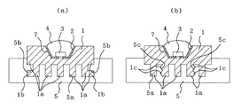
図1(a)、図1(b)は実施の形態1を示すLED照明装置の断面図、図2は図1(a)の分解斜視図である。
図1、図2において、LED照明装置は、表面に反射材2が設けられた凹部7を前面に有する基板1と、凹部7の底面に実装されたLED素子3と、LED素子を包み込むように溝部へ充填された樹脂4と、基板1の裏面に設けられた複数のフィン1aと、これらのフィン1aに対応して断面が凹凸形状に形成され、この凹状の溝部5aにフィン1aが各々着脱可能に嵌合される照明装置筐体5が設けられている。
1 (a) and 1 (b) are cross-sectional views of the LED illumination
In FIG. 1 and FIG. 2, the LED illumination device wraps the LED element, the
図1(a)に示すLED照明装置は、基板1の裏面に設けられた複数のフィン1aの内、両外側のフィン1aの端部の外側面に断面四辺形状の係止部1bが形成され、これらの係止部1bに対応する照明装置筐体5の溝部5aの内、これらの係止部1bに対応する両外側の溝部5aに係止部1bに係止される被係止部5bが形成されている。
また、基板1の各フィン1a、各係止部1b及びこれらに対応する各溝部5a、各被係止部5bは基板の凹部7の中心軸に対して左右対称であり、また、図2に示すように長手方向に沿って長い形状である。In the LED lighting device shown in FIG. 1A, a
Further, each
図1(b)に示すLED照明装置は、基板1の裏面に設けられた複数のフィン1aの内、外側から2番目のフィン1aの側面に断面三角形状の係止部1cが形成され、照明装置筐体5の溝部5aの内、これらの係止部1cに対応する外側から2番目の溝部5aに係止部1cに係止される被係止部5cが形成されている。
また、基板1の各フィン1a、各係止部1c及びこれらに対応する各溝部5a、各被係止部5cは、基板の凹部7の中心軸に対して左右対称であり、また、長手方向に沿って長い形状である。In the LED lighting device shown in FIG. 1B, a
Further, each
照明装置筐体5は熱伝導率の高い材料であり、基板1は例えばセラミック基板である。 その凹部7は底部が平面であり、前面から底部にかけて狭くなる連続斜面を有する。また、凹部7の表面に配置した反射材2は例えば銀であり、可視光領域での反射率が高く、凹部7の外へ光を効率よく発光することが可能となる。 The
LED素子3は例えばサファイア基板上に窒化ガリウム系の発光層から形成され、各層に接合された電極を前記溝部の底面に配置された配線部と電気的に接続することにより電力を提供する。さらに、LED素子3を包み込むように凹部へ充填された樹脂4は、エポキシ材やシリコン材などからなる透明あるいは半透明の樹脂であり、特に、紫外光などに対して劣化速度が緩やかなものなど耐候性の強いものが良い。 The
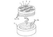
次に、基板1と照明装置筐体5の取り付けについて図1、図2により説明する。
基板1を照明装置筐体5に取り付けるときは、図2に示すように、基板1のフィン1a、係止部1bを照明装置筐体5の溝部5a、被係止部5bを各々合わせて、基板1を照明装置筐体5の横方向から挿入して嵌合させる。このとき、基板1のフィン1a、係止部1b及び照明装置筐体5の溝部5a、被係止部5bの各々の嵌合部に、熱伝導率の高いグリスを塗布する。また、基板1の両外側のフィン1aの外側面の係止部1bが、照明装置筐体5の両外側の溝部5aの被係止部5bに係止されて、基板1と照明装置筐体5を固定する。Next, attachment of the
When attaching the
図1(B)の場合も同様に、基板1のフィン1a、係止部1cを照明装置筐体5の溝部5a、被係止部5cを各々合わせて、基板1を照明装置筐体5の横方向から挿入嵌合させると、基板1の外側から2番目のフィン1aの外側面に形成された係止部1cが、照明装置筐体5の溝部5aの被係止部5cに係止されて、基板1と照明装置筐体5を固定する。 Similarly, in the case of FIG. 1B, the
以上のように、基板1の裏側に設けられた複数のフィン1aと、これらのフィン1aが各々着脱可能に嵌合される溝部5aを有する照明装置筐体5と、フィン1aの側面側に突設されフィンの一部をなす係止部1b、1cと、照明装置筐体5の溝部5aに形成され、係止部1b、1cに係止されて前記基板と前記照明装置筐体を固定する被係止部5b、5cとを備えたので、熱伝導率のより高い照明装置筐体との接触面積が大きくなり、LED素子より発生する熱を効率よく外部へ放熱し、LED素子の寿命特性や発光効率の悪化を防ぐと共に、LED素子周辺に充填した樹脂の劣化も防ぐことにより、信頼性を高くすることができ、また、基板に形成したフィンの一部を利用して、照明装置筐体への取り付けが可能であり、取り付けが容易でメンテナンス性を良くすることができる。
また、嵌合部には熱伝導率の高いグリスを塗布することにより、基板1で発生した熱をより効率的に照明装置筐体5へ放熱することができる。
また、係止部1b、1cは、基板1の凹部7の中心軸に対して左右対称に設けられたので、工作性を良くすることができる。As described above, the plurality of
Further, by applying grease having a high thermal conductivity to the fitting portion, the heat generated in the
Moreover, since the latching |
実施の形態2.
実施の形態1では、基板1の各フィン1a、各係止部1b及び照明装置筐体5の溝部5a、被係止部5bの側面の形状は、基板の凹部7の中心軸に対して、左右対称であるが、
本実施の形態は、基板1の凹部7の中心軸に対して、左右非対称としたものである。
In
This embodiment is asymmetrical with respect to the central axis of the
図3の(a)(b)はこの発明の実施の形態2を示すLED照明装置の断面図である。図において、実施の形態1と同一または相当部分には同一符号を付け説明を省略する。 3 (a) and 3 (b) are cross-sectional views of an LED illumination
図3(a)は基板1の両外側のフィン1aの一方の端部の外側面に突設した断面四辺形状の係止部1bを形成し、他方の端部の内側面に突設した断面四辺形状の係止部1dを形成している。これらの係止部1b、1dに対応して照明装置筐体5の溝部5aには、被係止部5b、5dを各々形成している。
また、基板1の各係止部1b、1d及びこれらに対応する各被係止部5b、5dは基板の凹部7の中心軸に対して左右非対称である。
図3(b)は基板1の一方の外側から2番目のフィン1aと他方の外側から1番目のフィン1aの外側面に断面三角形状の係止部1c、1eを各々形成し、これらの係止部1c、1eに対応して照明装置筐体5の溝部5aには、被係止部5c、5eを各々形成している。
また、基板1の各係止部1c、1e及びこれらに対応する各被係止部5c、5eは基板の凹部7の中心軸に対して各々非左右対称である。FIG. 3A shows a cross section in which a locking
Further, the
FIG. 3 (b) shows that engaging
Further, the
次に、基板1と照明装置筐体5の取り付けを説明する。
図3(a)の場合は、基板1の両外側のフィン1aの一方の端部の外側面に突設した係止部1bを照明装置筐体5の溝部5aの一方の被係止部5bに合わせ、また、基板1の他方の端部の内側面に突設した係止部1dを照明装置筐体5の溝部5aの他方の被係止部5dに合わせて、基板1を照明装置筐体5の横方向から挿入して嵌合させる。このとき、基板1の係止部1b、1dが、照明装置筐体5の被係止部5b、5dに各々係止されて、基板1と照明装置筐体5を固定する。Next, attachment of the board |
In the case of FIG. 3A, the locking
図3(b)の場合は、基板1の一方の外側から2番目のフィン1aと基板1の他方の外側から2番目のフィン1aの端部の外側面に突設した各々の係止部1c、1eを、被係止部5c、5eに合わせ、基板1を照明装置筐体5の横方向から挿入して嵌合させる。このとき、基板1の係止部1c、1eが照明装置筐体5の被係止部5c、5eに各々係止されて、基板1と照明装置筐体5を固定する。 In the case of FIG. 3B, each locking
以上のように、係止部1b、1d、または、係止部1c、1eを、基板1の凹部7の中心軸に対して、各々左右非対称としたので、基板1を照明装置筐体5へ取り付ける際の方向性を確定することができる。このことにより、基板1の誤挿入などを防止することができる。 As described above, since the locking
実施の形態3.
図4はこの発明の実施の形態3を示すLED照明装置の斜視図である。図において、実施の形態1と同一または相当部分には同一符号を付け説明を省略する。
FIG. 4 is a perspective view of an LED illumination
本実施の形態は、実施の形態1の図1(a)、図2に示した基板1の両側のフィン1aの一部である係止部1bを、図4に示すように各々長手方向に沿った長さが短い係止部1fとし、照明装置筐体5の被係止部5fに基板1の係止部1fが係止する係止位置とは異なった位置に、係止部1fが差し込まれる差し込み口5gを設けたものである。
図4では基板1と照明装置筐体5の一端部を示しているが、他端部も同じ構成である。In this embodiment, the locking
Although FIG. 4 shows one end of the
基板1を照明装置筐体5に取り付けるときは、基板1の両外側のフィン1aの係止部1fを、照明装置筐体5の被係止部5fに設けられた差し込み口5gに合わせて、基板1を照明装置筐体5の上方向から挿入し、挿入後、横方向にずらして照明装置筐体5の被係止部5fに基板1の係止部1fを係止させる。 When attaching the
以上のように、照明装置筐体5の被係止部5fに、フィン1aに設けた係止部1fが係止される係止位置とは異なった位置に、係止部1fが差し込まれる差し込み口5gを設けたので、基板1を照明装置筐体5へ取り付ける作業を容易にすることができ、メンテナンス性を良くすることができる。 As described above, the locking
実施の形態4.
図5はこの発明の実施の形態4を示すLED照明装置の断面図である。図において、実施の形態1と同一または相当部分には同一符号を付け説明を省略する。
FIG. 5 is a cross-sectional view of an LED lighting
図5において、LED素子3が実装される基板1の凹部7に近いのフィン1aの両側面とこのフィン1aが嵌合される照明装置筐体の溝部5aの両側面に、相互に接触するようにLED素子3の通電用の電極6が設けられている。 In FIG. 5, both side surfaces of the
この構成において、基板1を照明装置筐体5に取り付けると同時に、基板1のフィン1aの両側面と照明装置筐体の溝部5aの両側面に設けられた各々設けられた電極が接続される。 In this configuration, at the same time that the
以上のように、フィン1aとこのフィン1aが嵌合される照明装置筐体5の溝部5aに、相互に接触するようにLED素子3の通電用の電極を備えたので、基板1と照明装置筐体5の取り付けと同時に電気的接続がされ、電気的接続作業を省くことができる。 As described above, since the
実施の形態5.
図6の(a)(b)はこの発明の実施の形態5を示すLED照明装置の断面図、図7は図6(a)の分解斜視図である。図において、実施の形態1と同一または相当部分には同一符号を付け説明を省略する。
6 (a) and 6 (b) are cross-sectional views of an LED lighting
図6(a)に示すLED照明装置は、基板1の側面に突設されたフィン1a及びこのフィン1aに対応する照明装置筐体5の溝部5aが螺旋状に形成されており、フィン1aは係止部1hを兼ね、溝部5aは被係止部5hを兼ねている。
図6の(b)に示すLED照明装置は、基板1の裏側に複数のフィン1aが設けられ、フィン1aの内、外側のフィン1aの側面に断面三角形状の係止部1hが螺旋状に形成され、照明装置筐体5の外側の溝部5aに係止部1hに係止される被係止部5hが螺旋状に形成されている。In the LED illumination device shown in FIG. 6A, a
In the LED lighting device shown in FIG. 6B, a plurality of
基板1を照明装置筐体5に取り付けるときは、基板1のフィン1a(係止部1h)を、照明装置筐体5の溝部5a(被係止部5h)にねじ込んで固定する。 When attaching the board |
以上のように、フィン1aの一部をなす係止部1hを、螺旋状に形成したので、基板1を照明装置筐体5へ取り付ける作業を容易にするとともに、基板1を確実に装着することができる。
なお、本実施の形態では、係止部1hを外側に設け、断面三角形状としたが、外側から例えば2番目でもよく、断面を4辺形状としてもよい。As described above, since the locking
In the present embodiment, the locking
1 基板、1a フィン、1b、1c、1d、1e、1f、1h 係止部、2 反射材、3 LED素子、4 樹脂、5 照明装置筐体、5a 溝部、5b、5c、5d、5e、5f、5h 被係止部、5g 差し込み口、6 電極。
1 Substrate, 1a Fin, 1b, 1c, 1d, 1e, 1f, 1h Locking portion, 2 Reflective material, 3 LED element, 4 Resin, 5 Illuminating device housing, 5a Groove, 5b, 5c, 5d, 5e, 5f 5h Locked part, 5g insertion port, 6 electrodes.
Claims (1)
Translated fromJapanese前記凹部の底面に実装されたLED素子と、
前記基板の裏側に同心円状に形成された複数のフィンと、
該複数のフィンのうち、最も外側のフィンの外側面に螺旋状に形成され該フィンの一部をなす係止部と、
該係止部が嵌合される螺旋状に形成された溝部を有する照明装置筐体と、
を備えたことを特徴とするLED照明装置。A substrate having a concave portion provided with a reflector on the front surface;
LED elements mounted on the bottom surface of the recess,
A plurality of fins formed concentrically on the back side of the substrate;
A locking portion that is spirally formed on the outer surface of the outermost fin among the plurality of fins and forms a part of the fin;
A lighting device housing having a spirally formed groove portion into which the locking portion is fitted;
An LED lighting device comprising:
Priority Applications (1)
| Application Number | Priority Date | Filing Date | Title |
|---|---|---|---|
| JP2005223247AJP4740682B2 (en) | 2005-08-01 | 2005-08-01 | LED lighting device |
Applications Claiming Priority (1)
| Application Number | Priority Date | Filing Date | Title |
|---|---|---|---|
| JP2005223247AJP4740682B2 (en) | 2005-08-01 | 2005-08-01 | LED lighting device |
Publications (2)
| Publication Number | Publication Date |
|---|---|
| JP2007042755A JP2007042755A (en) | 2007-02-15 |
| JP4740682B2true JP4740682B2 (en) | 2011-08-03 |
Family
ID=37800482
Family Applications (1)
| Application Number | Title | Priority Date | Filing Date |
|---|---|---|---|
| JP2005223247AExpired - LifetimeJP4740682B2 (en) | 2005-08-01 | 2005-08-01 | LED lighting device |
Country Status (1)
| Country | Link |
|---|---|
| JP (1) | JP4740682B2 (en) |
Families Citing this family (15)
| Publication number | Priority date | Publication date | Assignee | Title |
|---|---|---|---|---|
| JP5122172B2 (en) | 2007-03-30 | 2013-01-16 | ローム株式会社 | Semiconductor light emitting device |
| TWI406044B (en)* | 2007-12-31 | 2013-08-21 | Hannstar Display Corp | Backlight module and light-emitting device thereof |
| KR101596893B1 (en)* | 2008-06-26 | 2016-02-24 | 서울반도체 주식회사 | Heat radiating led mount and lamp |
| KR101574648B1 (en) | 2009-03-30 | 2015-12-07 | 서울반도체 주식회사 | Lighting equipment |
| KR100980588B1 (en)* | 2009-08-27 | 2010-09-06 | 윤인숙 | Led lamp |
| KR101125296B1 (en)* | 2009-10-21 | 2012-03-27 | 엘지이노텍 주식회사 | Light unit |
| CN102022658A (en)* | 2010-12-29 | 2011-04-20 | 东莞市华胜展鸿电子科技有限公司 | Light emitting diode lamp |
| EP2767757A4 (en)* | 2011-10-10 | 2015-03-18 | Posco Led Co Ltd | SEMICONDUCTOR LIGHTING OPTICAL APPARATUS |
| WO2013072805A1 (en)* | 2011-11-17 | 2013-05-23 | Koninklijke Philips Electronics N.V. | Solid state lighting module with improved heat spreader |
| WO2016079900A1 (en)* | 2014-11-19 | 2016-05-26 | アイリスオーヤマ株式会社 | Lighting device |
| JP6341949B2 (en) | 2016-04-04 | 2018-06-13 | 中村 正一 | LED lighting device |
| US10584845B2 (en) | 2017-05-12 | 2020-03-10 | Shoichi Nakamura | LED lighting apparatus |
| US10141489B1 (en) | 2017-08-24 | 2018-11-27 | Shoichi Nakamura | LED illumination apparatus |
| US10197261B1 (en) | 2017-11-03 | 2019-02-05 | Shoichi Nakamura | LED illumination apparatus with heat sink having a portion of heat fins exposed to axial forced flow from a cooling fan |
| DE102022111490A1 (en)* | 2022-05-09 | 2023-11-09 | HELLA GmbH & Co. KGaA | Light module for a motor vehicle lighting device and method for producing a light module |
Family Cites Families (7)
| Publication number | Priority date | Publication date | Assignee | Title |
|---|---|---|---|---|
| JPS60253284A (en)* | 1984-05-29 | 1985-12-13 | Fuji Photo Film Co Ltd | semiconductor light source device |
| JPH0282659A (en)* | 1988-09-20 | 1990-03-23 | Ngk Insulators Ltd | Optical transmitter |
| JPH031585A (en)* | 1989-05-29 | 1991-01-08 | Fanuc Ltd | Discharge tube for laser oscillator |
| JP2001329729A (en)* | 2000-05-22 | 2001-11-30 | Yutaka Denshi Kk | Opening restricting lock device for door |
| JP4689880B2 (en)* | 2001-06-27 | 2011-05-25 | スワン商事株式会社 | Sash that can be folded and folded |
| JP2003243718A (en)* | 2002-02-14 | 2003-08-29 | Matsushita Electric Works Ltd | Light emitting device |
| JP3653090B1 (en)* | 2004-04-09 | 2005-05-25 | シーシーエス株式会社 | Light irradiation device |
- 2005
- 2005-08-01JPJP2005223247Apatent/JP4740682B2/ennot_activeExpired - Lifetime
Also Published As
| Publication number | Publication date |
|---|---|
| JP2007042755A (en) | 2007-02-15 |
Similar Documents
| Publication | Publication Date | Title |
|---|---|---|
| JP4740682B2 (en) | LED lighting device | |
| JP4241658B2 (en) | Light emitting diode light source unit and light emitting diode light source formed using the same | |
| JP4980152B2 (en) | Lighting device | |
| US7452110B2 (en) | Light emitting device | |
| US20130093359A1 (en) | Lighting device | |
| KR100948115B1 (en) | Led lighting device | |
| TW201323767A (en) | Street lamp, illuminating device and its lighting module | |
| JP4941207B2 (en) | Illumination unit and illumination lamp using the same | |
| JP6138816B2 (en) | LED lighting device | |
| US8256928B2 (en) | Light-emitting diode lamp with radiation mechanism | |
| JP4602477B1 (en) | Lighting device | |
| JP4812828B2 (en) | LED lighting device | |
| KR101099572B1 (en) | LED lighting device | |
| KR20140122474A (en) | Led lamp assembly | |
| KR101933046B1 (en) | Boltless-type illuminating device | |
| JP6085459B2 (en) | Lighting device | |
| JP2013065442A (en) | Lighting device | |
| KR101201607B1 (en) | Light fixture for vehicle | |
| KR101876948B1 (en) | Illuminating lamp | |
| KR101175754B1 (en) | Light emitting device | |
| JP2006319290A (en) | Light emitting diode light source unit and valve type thereof | |
| JP6658919B2 (en) | lamp | |
| JP2006310515A (en) | Light emitting unit | |
| JP2019102398A (en) | Vehicular lighting fixture | |
| JP5487505B2 (en) | LED lamp |
Legal Events
| Date | Code | Title | Description |
|---|---|---|---|
| A621 | Written request for application examination | Free format text:JAPANESE INTERMEDIATE CODE: A621 Effective date:20080121 | |
| A977 | Report on retrieval | Free format text:JAPANESE INTERMEDIATE CODE: A971007 Effective date:20100901 | |
| A131 | Notification of reasons for refusal | Free format text:JAPANESE INTERMEDIATE CODE: A131 Effective date:20100907 | |
| A521 | Request for written amendment filed | Free format text:JAPANESE INTERMEDIATE CODE: A523 Effective date:20101029 | |
| A02 | Decision of refusal | Free format text:JAPANESE INTERMEDIATE CODE: A02 Effective date:20110111 | |
| A521 | Request for written amendment filed | Free format text:JAPANESE INTERMEDIATE CODE: A523 Effective date:20110223 | |
| A911 | Transfer to examiner for re-examination before appeal (zenchi) | Free format text:JAPANESE INTERMEDIATE CODE: A911 Effective date:20110316 | |
| TRDD | Decision of grant or rejection written | ||
| A01 | Written decision to grant a patent or to grant a registration (utility model) | Free format text:JAPANESE INTERMEDIATE CODE: A01 Effective date:20110426 | |
| A01 | Written decision to grant a patent or to grant a registration (utility model) | Free format text:JAPANESE INTERMEDIATE CODE: A01 | |
| A61 | First payment of annual fees (during grant procedure) | Free format text:JAPANESE INTERMEDIATE CODE: A61 Effective date:20110502 | |
| R150 | Certificate of patent or registration of utility model | Ref document number:4740682 Country of ref document:JP Free format text:JAPANESE INTERMEDIATE CODE: R150 Free format text:JAPANESE INTERMEDIATE CODE: R150 | |
| FPAY | Renewal fee payment (event date is renewal date of database) | Free format text:PAYMENT UNTIL: 20140513 Year of fee payment:3 | |
| R250 | Receipt of annual fees | Free format text:JAPANESE INTERMEDIATE CODE: R250 | |
| R250 | Receipt of annual fees | Free format text:JAPANESE INTERMEDIATE CODE: R250 | |
| R250 | Receipt of annual fees | Free format text:JAPANESE INTERMEDIATE CODE: R250 | |
| R250 | Receipt of annual fees | Free format text:JAPANESE INTERMEDIATE CODE: R250 | |
| R250 | Receipt of annual fees | Free format text:JAPANESE INTERMEDIATE CODE: R250 | |
| R250 | Receipt of annual fees | Free format text:JAPANESE INTERMEDIATE CODE: R250 | |
| R250 | Receipt of annual fees | Free format text:JAPANESE INTERMEDIATE CODE: R250 | |
| R250 | Receipt of annual fees | Free format text:JAPANESE INTERMEDIATE CODE: R250 | |
| R250 | Receipt of annual fees | Free format text:JAPANESE INTERMEDIATE CODE: R250 |